WO2012140942A1 - 発光装置、発光装置の製造方法、照明装置、バックライトおよび表示装置 - Google Patents
発光装置、発光装置の製造方法、照明装置、バックライトおよび表示装置 Download PDFInfo
- Publication number
- WO2012140942A1 WO2012140942A1 PCT/JP2012/052712 JP2012052712W WO2012140942A1 WO 2012140942 A1 WO2012140942 A1 WO 2012140942A1 JP 2012052712 W JP2012052712 W JP 2012052712W WO 2012140942 A1 WO2012140942 A1 WO 2012140942A1
- Authority
- WO
- WIPO (PCT)
- Prior art keywords
- light emitting
- electrode
- emitting device
- rod
- light
- Prior art date
- Legal status (The legal status is an assumption and is not a legal conclusion. Google has not performed a legal analysis and makes no representation as to the accuracy of the status listed.)
- Ceased
Links
Images












Classifications
-
- G—PHYSICS
- G02—OPTICS
- G02F—OPTICAL DEVICES OR ARRANGEMENTS FOR THE CONTROL OF LIGHT BY MODIFICATION OF THE OPTICAL PROPERTIES OF THE MEDIA OF THE ELEMENTS INVOLVED THEREIN; NON-LINEAR OPTICS; FREQUENCY-CHANGING OF LIGHT; OPTICAL LOGIC ELEMENTS; OPTICAL ANALOGUE/DIGITAL CONVERTERS
- G02F1/00—Devices or arrangements for the control of the intensity, colour, phase, polarisation or direction of light arriving from an independent light source, e.g. switching, gating or modulating; Non-linear optics
- G02F1/01—Devices or arrangements for the control of the intensity, colour, phase, polarisation or direction of light arriving from an independent light source, e.g. switching, gating or modulating; Non-linear optics for the control of the intensity, phase, polarisation or colour
- G02F1/13—Devices or arrangements for the control of the intensity, colour, phase, polarisation or direction of light arriving from an independent light source, e.g. switching, gating or modulating; Non-linear optics for the control of the intensity, phase, polarisation or colour based on liquid crystals, e.g. single liquid crystal display cells
- G02F1/133—Constructional arrangements; Operation of liquid crystal cells; Circuit arrangements
- G02F1/1333—Constructional arrangements; Manufacturing methods
- G02F1/1335—Structural association of cells with optical devices, e.g. polarisers or reflectors
- G02F1/1336—Illuminating devices
- G02F1/133602—Direct backlight
- G02F1/133603—Direct backlight with LEDs
-
- H—ELECTRICITY
- H05—ELECTRIC TECHNIQUES NOT OTHERWISE PROVIDED FOR
- H05B—ELECTRIC HEATING; ELECTRIC LIGHT SOURCES NOT OTHERWISE PROVIDED FOR; CIRCUIT ARRANGEMENTS FOR ELECTRIC LIGHT SOURCES, IN GENERAL
- H05B45/00—Circuit arrangements for operating light-emitting diodes [LED]
- H05B45/40—Details of LED load circuits
- H05B45/44—Details of LED load circuits with an active control inside an LED matrix
-
- H—ELECTRICITY
- H10—SEMICONDUCTOR DEVICES; ELECTRIC SOLID-STATE DEVICES NOT OTHERWISE PROVIDED FOR
- H10H—INORGANIC LIGHT-EMITTING SEMICONDUCTOR DEVICES HAVING POTENTIAL BARRIERS
- H10H20/00—Individual inorganic light-emitting semiconductor devices having potential barriers, e.g. light-emitting diodes [LED]
- H10H20/80—Constructional details
- H10H20/81—Bodies
- H10H20/817—Bodies characterised by the crystal structures or orientations, e.g. polycrystalline, amorphous or porous
- H10H20/818—Bodies characterised by the crystal structures or orientations, e.g. polycrystalline, amorphous or porous within the light-emitting regions
-
- H—ELECTRICITY
- H10—SEMICONDUCTOR DEVICES; ELECTRIC SOLID-STATE DEVICES NOT OTHERWISE PROVIDED FOR
- H10H—INORGANIC LIGHT-EMITTING SEMICONDUCTOR DEVICES HAVING POTENTIAL BARRIERS
- H10H20/00—Individual inorganic light-emitting semiconductor devices having potential barriers, e.g. light-emitting diodes [LED]
- H10H20/80—Constructional details
- H10H20/81—Bodies
- H10H20/819—Bodies characterised by their shape, e.g. curved or truncated substrates
- H10H20/821—Bodies characterised by their shape, e.g. curved or truncated substrates of the light-emitting regions, e.g. non-planar junctions
Definitions
- the present invention relates to a light emitting device, a method for manufacturing the light emitting device, a lighting device, a backlight, and a display device.
- Patent Document 1 Japanese Patent Laid-Open No. 2002-173028
- the parallel light emitting device shown in FIG. 19 is strong against open mode defects, but is weak against variations in element characteristics due to low voltage driving, and is also vulnerable to short mode defects. Yes (if the current continues to flow through the light emitting diode in the short mode, no current flows through the other light emitting diodes).
- the series-parallel light emitting device shown in FIG. 20 has both advantages and disadvantages of the light emitting device shown in FIGS.
- an object of the present invention is to provide a light emitting device and a method for manufacturing the light emitting device with high yield by suppressing variations in light emission characteristics in a light emitting device using a fine rod-shaped light emitting diode.
- Another object of the present invention is to provide a lighting device, a backlight, and a display device with high yield while suppressing variations in light emission characteristics.
- a light-emitting device of the present invention includes: A light emitting diode parallel circuit in which rod-shaped light emitting diodes are connected in parallel is connected in series, and a grid-like array in which the bar-shaped light emitting diodes are arranged in a grid, A first electrode connected to one end of the grid array; A second electrode connected to the other end of the grid array,
- the rod-shaped structure light emitting diode includes a rod-shaped first-conductivity-type semiconductor core having a length to diameter ratio of 5 to 200 and a diameter of 500 nm to 100 ⁇ m, and a cylinder surrounding the semiconductor core And a second conductive type semiconductor layer.
- the diameter of the semiconductor core is set to 500 nm or more and 100 ⁇ m or less, variation in the diameter of the semiconductor core can be suppressed as compared with the semiconductor core having a diameter of several tens to several hundreds of nm. Therefore, in a light-emitting device using a fine rod-shaped light-emitting diode, a light-emitting device with high yield can be realized while suppressing variations in light emission characteristics.
- the grid array has a plurality of subarrays in which a plurality of the light emitting diode parallel circuits are connected in series, The plurality of subarrays are connected in parallel between the first electrode and the second electrode.
- the plurality of subarrays are arranged such that all of the rod-shaped structure light emitting diodes are in a forward direction toward the first electrode side or the second electrode side,
- the number of the bar-shaped light emitting diodes in the light emitting diode parallel circuit of each subarray is 35 or more.
- the plurality of sub-arrays are connected to the rod-shaped structure light emitting diodes connected in the forward direction toward the first electrode side, and connected to be set in the forward direction toward the second electrode side.
- Rod-shaped structure light emitting diodes are randomly arranged, The number of the bar-shaped light emitting diodes in the light emitting diode parallel circuit of each subarray is 70 or more.
- the plurality of subarrays are classified into a plurality of subarray groups, A power supply unit for supplying a power supply voltage is provided for each of the subarray groups.
- the power supply unit is different in the other subarray groups and the influence on the supplied power supply voltage is small. Can be reduced.
- the grid array is connected to the rod-shaped structure light emitting diodes connected in a forward direction toward the first electrode side, and connected to the forward direction toward the second electrode side.
- the rod-shaped structure light emitting diodes are arranged at random.
- the above embodiment it is possible to realize driving by an AC operation by applying an AC voltage between the first electrode and the second electrode.
- the manufacturing process can be simplified and the manufacturing cost can be reduced.
- a plurality of light emitting diode parallel circuits in which rod-shaped light emitting diodes are connected in parallel are connected in series, and the rod-shaped light emitting diodes are connected in a grid pattern, and are connected to one end of the grid array.
- the grid array has a plurality of subarrays in which a plurality of the light emitting diode parallel circuits are connected in series, A defect determination step for determining the presence or absence of defects for the plurality of subarrays; Of the plurality of subarrays, a connection between the subarray determined to be defective in the defect determination step and the first electrode, or a connection between the subarray determined to be defective in the defect determination step and the second electrode And a separation step of separating at least one of the above.
- the manufacturing yield can be increased. Therefore, by using a fine rod-shaped light emitting diode having a length ratio to the semiconductor core diameter of 5 or more and 200 or less and a semiconductor core diameter of 500 nm or more and 100 ⁇ m or less, variation in light emission characteristics is suppressed. In addition, a light-emitting device with high yield can be realized.
- a wiring that connects one end of the subarray determined to be defective and the first electrode, or a wiring that connects the other end of the subarray determined to be defective and the second electrode At least one is cut with a laser.
- each subarray Prior to the defect determination step, each subarray is connected to one end of the subarray and the first electrode, or to at least one of the other end of the subarray and the second electrode.
- a transistor forming step of forming a transistor Prior to the defect determination step, each subarray is connected to one end of the subarray and the first electrode, or to at least one of the other end of the subarray and the second electrode.
- the separation step between the one end of the subarray determined to be defective in the defect determination step and the first electrode, or the other end of the subarray determined to be defective and the first A transistor connected to at least one of the two electrodes is turned off during light emission operation by gate control.
- the transistor is a thin film transistor.
- the transistor can be manufactured at low cost.
- the grid array By applying a voltage between the first electrode and the second electrode, and passing a preset current through the grid array for a preset time, the grid array A screening step for screening the rod-shaped structure light emitting diode is included.
- the rod-shaped structure light emitting diode is applied to the rod-shaped structure light-emitting diode. Screening step of performing screening.
- substantially the same voltage is applied to all the bar-shaped light emitting diodes connected in parallel, and a current corresponding to the characteristic variation flows. Can be more efficiently reduced.
- any one of the above light emitting devices is provided.
- the light emitting device and the method for manufacturing the light emitting device of the present invention in the light emitting device using the fine rod-shaped light emitting diode, the light emitting device and the light emitting device with high yield can be suppressed by suppressing variation in the light emission characteristics.
- An apparatus manufacturing method can be realized.
- the lighting device, backlight and display device of the present invention it is possible to realize a lighting device, backlight and display device with high yield while suppressing variations in light emission characteristics.
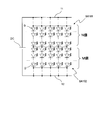
- FIG. 1A is a circuit diagram of a light emitting device according to a first embodiment of the present invention.
- FIG. 1B is a circuit diagram of another example of the light emitting device.
- FIG. 1C is a circuit diagram of another example of the light emitting device.
- FIG. 2 is a schematic side view of a light emitting diode as an example of a rod-shaped structure light emitting element of the light emitting device of the light emitting device.
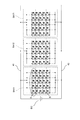
- FIG. 3 is a circuit diagram of a light emitting device according to a second embodiment of the present invention.
- FIG. 4 is a circuit diagram of a light emitting device according to a third embodiment of the present invention.
- FIG. 5 is a circuit diagram of a light emitting device according to a fourth embodiment of the present invention.
- FIG. 1A is a circuit diagram of a light emitting device according to a first embodiment of the present invention.
- FIG. 1B is a circuit diagram of another example of the light emitting device.
- FIG. 6 is a cross-sectional view of a main part of the light emitting device.
- FIG. 7 is a diagram showing the relationship of the relative light quantity with respect to the number of parallel elements of the light emitting device.
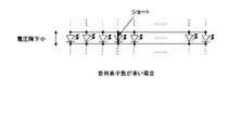
- FIG. 8 is a circuit diagram of a main part of the light emitting device when the number of parallel elements is large.
- FIG. 9 is a circuit diagram of the main part of the light emitting device when the number of parallel elements is small.
- FIG. 10 is a diagram showing the relationship of the relative light quantity with respect to the number of parallel elements of the light emitting device.
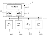
- FIG. 11A is a block diagram showing a configuration of a light emitting device according to the fifth embodiment of the present invention.
- FIG. 11B is a circuit diagram of a subarray of the light emitting device.
- FIG. 11A is a block diagram showing a configuration of a light emitting device according to the fifth embodiment of the present invention.
- FIG. 11B is a circuit diagram of a subarray of the light
- FIG. 11C is a block diagram showing a modification of the light emitting device of the fifth embodiment.
- FIG. 12 is a circuit diagram of a light emitting device according to a sixth embodiment of the present invention.
- FIG. 13 is a circuit diagram of a light emitting device according to a seventh embodiment of the present invention.
- FIG. 14 is a plan view and an equivalent circuit showing a state in which all the bar-shaped light emitting diodes of the light emitting device according to the eighth embodiment of the present invention are connected in parallel.
- FIG. 15 is a plan view and an equivalent circuit showing a state in which light-emitting diode parallel circuits are connected in series.
- FIG. 16 is a view for explaining a screening method for a light emitting device according to the ninth embodiment of the present invention.
- FIG. 17 is a diagram for explaining the second screening method.
- FIG. 18 is a circuit diagram of a conventional light emitting device in which a plurality of light emitting diodes are connected in series.
- FIG. 19 is a circuit diagram of a conventional light emitting device in which a plurality of light emitting diodes are connected in parallel.
- FIG. 20 is a circuit diagram of a conventional light emitting device having a configuration in which subarrays each having a plurality of light emitting diodes connected in series are connected in parallel.
- FIG. 1A shows a circuit diagram of a light emitting device according to a first embodiment of the present invention.
- the light emitting device according to the first embodiment includes a grid array A1 in which a plurality of bar-shaped light emitting diodes D are arranged in a grid pattern.
- a plurality of bar-shaped light emitting diodes D are arranged in a grid by connecting a plurality of light-emitting diode parallel circuits each having a bar-shaped light-emitting diode D connected in parallel.
- the light-emitting device includes a first electrode 11 connected to one end of the grid array A1, and a second electrode 12 connected to the other end of the grid array A1.
- the positive electrode side output terminal of the DC power source DC is connected to the first electrode 11, and the negative electrode side output terminal of the DC power source DC is connected to the second electrode 12.
- the grid array A1 is arranged so that all of the rod-shaped light emitting diodes D are in the forward direction toward the second electrode 12 side. That is, the cathode side of the rod-shaped structure light-emitting diode D is directed to the second electrode 12 side, and the anode side of the rod-shaped structure light-emitting diode D is directed to the first electrode 11 side.
- a plurality of subarrays SA101 in which a plurality of light emitting diode series circuits in which N (N is an integer of 2 or more) rod-shaped structure light emitting diodes D are connected in series are connected in series are connected.
- N is an integer of 2 or more rod-shaped structure light emitting diodes D
- a plurality of rod-shaped structure light emitting diodes D may be arranged in a lattice pattern. In this case, it is effective when there are many short-circuit defects of the rod-shaped structure light emitting diode D.
- a plurality of subarrays SA101 in which a plurality of light emitting diode series circuits in which N (N is an integer of 2 or more) rod-shaped light emitting diodes D are connected in series are connected in series are connected.
- the number of rod-shaped light emitting diodes D connected in series in the series circuit need not be the same. For example, as shown in FIG.
- subarray SA101 in which a plurality of light emitting diode series circuits in which N (N is an integer of 2 or more) rod-shaped structure light emitting diodes D are connected in series are connected in parallel
- M M May be connected in series to a sub-array SA102 in which a plurality of LED series circuits each having a rod-shaped structure LED D connected in series are connected in parallel.
- FIG. 2 shows a schematic side view of the rod-shaped light emitting diode D of the light emitting device.
- the bar-shaped light emitting diode D has a semiconductor core 1 made of n-type GaN having a substantially hexagonal cross section and a semiconductor layer 2 made of cylindrical p-type GaN surrounded by the semiconductor core 1.
- the semiconductor core 1 has a length ratio to the diameter of 5 to 200 and a diameter of 500 nm to 100 ⁇ m, thereby suppressing variations in the diameter of the semiconductor core 1.
- the second power flows from the positive output terminal of the DC power source DC to each bar-shaped light emitting diode D of the grid array A1 through the first electrode 11, and the second Return to the negative output terminal of the DC power source DC via the electrode 12.
- each bar-shaped light emitting diode D emits light.
- the amount of light can be greatly reduced because a current path exists in the other bar-shaped light emitting diodes D. Absent. Even if one of the rod-shaped light emitting diodes D of the grid array A1 is short-circuited, only the bar-shaped light-emitting diode D of the light-emitting diode parallel circuit including the bar-shaped light-emitting diode D having the short-circuit failure is generated. It is only affected and does not reduce the amount of light in other light emitting diode parallel circuits.
- the light emitting device of the first embodiment it is possible to realize a light emitting device with a high yield while suppressing variations in light emission characteristics.
- Such a bar-shaped light-emitting diode D can be manufactured at a lower cost than the conventional method by cutting the bar-shaped light-emitting diodes grown vertically on the substrate and arranging them again on the substrate. Manufacturing costs can be reduced.
- cut bar-shaped light-emitting diodes D are arranged again on the substrate, a larger number of open defects (non-conducting mode defects) due to poor arrangement occur than in the conventional method, but the circuit configuration shown in FIG. 1A is adopted. As a result, resistance to open defects is increased, and the manufacturing yield can be increased.
- FIG. 3 shows a circuit diagram of a light emitting device according to a second embodiment of the present invention.
- the light emitting device of the second embodiment has the same configuration as that of the light emitting device of the first embodiment except for the arrangement of the rod-shaped light emitting diodes D and the power source.
- the light emitting device includes a grid array A2 in which a plurality of bar-shaped light emitting diodes D are arranged in a grid pattern.
- a plurality of bar-shaped light emitting diodes D are arranged in a grid by connecting a plurality of light-emitting diode parallel circuits each having a bar-shaped light-emitting diode D connected in parallel.
- the light-emitting device includes a first electrode 21 connected to one end of the grid array A2, and a second electrode 22 connected to the other end of the grid array A2.
- One output terminal of the AC power supply AC is connected to the first electrode 21, and the other output terminal of the AC power supply AC is connected to the second electrode 22.
- the grid array A2 has the rod-shaped light emitting diode D connected so as to be in the forward direction toward the first electrode 21 and the forward direction toward the second electrode 22.
- the connected rod-shaped structure light emitting diodes D are arranged at random.
- an alternating current flows from the alternating current power supply AC to each bar-shaped light emitting diode D of the grid array A1 through the first electrode 21 and the second electrode 22.
- each bar-shaped light emitting diode D emits light.
- the light emitting device of the second embodiment it is possible to realize a light emitting device with a high yield while suppressing variations in light emission characteristics.
- the light emitting device of the second embodiment has the same effect as the light emitting device of the first embodiment. Further, in AC operation, it is not necessary to perform polarity control when arranging the rod-shaped structure light emitting diodes D, and circuit operation can be realized at low cost.
- the circuit operation is substantially impossible in the conventional configuration connected in series, whereas in the light emitting device of the second embodiment, AC Driving by operation can be realized, and it is not necessary to arrange the rod-shaped light emitting diodes in the forward direction in the same direction. Therefore, the manufacturing process can be simplified and the manufacturing cost can be reduced.
- FIG. 4 shows a circuit diagram of a light emitting device according to a third embodiment of the present invention.
- the light emitting device according to the third embodiment has the same configuration as that of the light emitting device according to the second embodiment except for the arrangement of the rod-shaped light emitting diodes D.
- the light emitting device of the third embodiment has subarrays SA1, SA2, SA3,... In which rod-shaped light emitting diodes D are formed in a lattice shape.
- a plurality of subarrays SA1, SA2, SA3,... Constitute a grid array.
- a plurality of bar-shaped light-emitting diodes D are arranged in a grid by connecting a plurality of light-emitting diode parallel circuits each having a bar-shaped light-emitting diode D connected in parallel. is doing.
- the plurality of subarrays SA1, SA2, SA3,... are connected in parallel between the first electrode 31 and the second electrode 32.
- One output terminal of the AC power supply AC is connected to the first electrode 31, and the other output terminal of the AC power supply AC is connected to the second electrode 32.
- the subarrays SA1, SA2, SA3,... are in a forward direction toward the first electrode 31 side and the rod-shaped structure light emitting diode D connected so as to be in the forward direction toward the first electrode 31 side.
- the rod-shaped structure light emitting diodes D connected in this manner are randomly arranged.
- an alternating current flows from the alternating-current power supply AC to the rod-shaped light-emitting diodes D of the subarrays SA1, SA2, SA3,. Thereby, each bar-shaped light emitting diode D emits light.
- the light emitting device of the third embodiment has the same effect as the light emitting device of the second embodiment.
- a plurality of subarrays SA1, SA2, SA3,... are provided, and the subarrays SA1, SA2, SA3,. Since the probability of occurrence of a pass can be reduced, it is possible to reduce the occurrence of a light emission failure due to a short failure of the rod-shaped light emitting diode D.
- the resistance to the open failure of the bar-shaped light emitting diode D is strong, but when the parallel number of the bar-shaped light emitting diodes D in the light emitting diode parallel circuit is increased, The possibility of light emission failure due to short-circuit failure (short-circuit mode failure) of the rod-shaped structure light emitting diode D increases. That is, there is a possibility that a series connection path of the bar-shaped light-emitting diodes D having a short-circuit will occur, and a sufficient current may not flow through the normal bar-shaped light-emitting diodes D in the grid array.
- FIG. 5 shows a circuit diagram of a light emitting device according to a fourth embodiment of the present invention.
- the light emitting device of the fourth embodiment has the same configuration as the light emitting device of the third embodiment except for the arrangement of rod-shaped light emitting diodes D and the power source.
- the plurality of subarrays SA11, SA12, SA13,... are arranged such that all of the rod-shaped structure light emitting diodes D are in the forward direction toward the second electrode 12 side. Is different from the light emitting device of the third embodiment.
- the light emitting device of the third embodiment has subarrays SA11, SA12, SA13,... In which rod-shaped light emitting diodes D are formed in a lattice shape.
- a plurality of subarrays SA11, SA12, SA13,... Constitute a grid array.
- a plurality of bar-shaped light-emitting diodes D are arranged in a grid by connecting a plurality of light-emitting diode parallel circuits each having a bar-shaped light-emitting diode D connected in parallel. is doing.
- the plurality of subarrays SA11, SA12, SA13,... are connected in parallel between the first electrode 41 and the second electrode.
- the positive electrode side output terminal of the DC power source DC is connected to the first electrode 41, and the negative electrode side output terminal of the DC power source DC is connected to the second electrode 42.
- the subarrays SA11, SA12, SA13,... are arranged so that all of the plurality of rod-shaped light emitting diodes D are in the forward direction toward the second electrode 42 side. That is, the cathode side of the rod-shaped structure light-emitting diode D is directed to the second electrode 42 side, and the anode side of the rod-shaped structure light-emitting diode D is directed to the first electrode 41 side.
- the second electrode 42 flows from the positive output terminal of the DC power source DC to the rod-shaped light emitting diodes D of the subarrays SA1, SA2, SA3,. To the negative output terminal of the DC power source DC. Thereby, each bar-shaped light emitting diode D emits light.
- the light emitting device of the fourth embodiment has the same effect as the light emitting device of the first embodiment.
- FIG. 6 is a cross-sectional view of the main part of the light emitting device.
- the rod-shaped structure light emitting diode D is formed on the substrate 40 so as to straddle the first electrode 41 and the second electrode 42 formed on the substrate 40. It is mounted parallel to the mounting surface. Then, one end (anode) of the rod-shaped structure light emitting diode D and the first electrode 41 are electrically connected by an adhesive portion 43 made of metal ink such as a conductive adhesive, and the other end of the rod-shaped structure light emitting diode D is connected to the other end.
- the exposed portion (cathode) of the exposed semiconductor core 1 and the second electrode 42 are electrically connected by an adhesive portion 44 made of metal ink such as a conductive adhesive.
- the outer periphery of the semiconductor layer 2 is covered with a conductive layer 3 having a resistance lower than that of the semiconductor layer 2.
- a short circuit may occur between the semiconductor core 1 on the first electrode 41 side and the semiconductor layer 2 as an example of a short circuit defect (region S shown in FIG. 6). ).
- the number of subarrays is set to 20 and the number of parallel elements is set to 35 or more. Further, the influence on other normal elements (in the light emitting diode parallel circuit) due to the short-circuit failure of the rod-shaped light emitting diode D can be reduced. That is, the LED parallel circuit shown in FIG. 8 with many rod-shaped light emitting diodes D connected in parallel has a rod-shaped structure light emission than the LED parallel circuit shown in FIG. 9 with few rod-shaped light emitting diodes D connected in parallel.
- a voltage drop across the light emitting diode parallel circuit due to a short circuit failure of the diode D is small. Such an effect is obtained from the resistance balance between the normal bar-shaped light-emitting diode D connected in parallel and the bar-shaped light-emitting diode D having a short-circuit failure, so that the influence of the number of series stages is small.
- the number of parallel elements of the bar-shaped light emitting diodes D of the light-emitting diode parallel circuit is set to 35 or more, thereby It is possible to suppress a voltage drop due to a short circuit failure of D, and to reduce the occurrence of light emission failure.
- the number of subarrays to 20 and the number of parallel elements to 70 or more, to other normal elements (inside the light emitting diode parallel circuit) due to short-circuit failure of the rod-shaped light emitting diode D. Is less affected.
- the number of parallel elements of the rod-shaped light emitting diodes D of the light emitting diode parallel circuit is set to 70 or more. It is possible to suppress a voltage drop caused by the light emission, and to reduce the occurrence of light emission failure.
- FIG. 11A shows a circuit diagram of a light emitting device according to a fifth embodiment of the present invention.
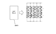
- the light emitting device of the fifth embodiment includes a power supply block 50 and subarrays SA51, SA52, SA53, SA54,... Supplied with a power supply voltage from the power supply block 50.
- the power supply block 50 includes a main power supply unit 51 and sub power supply units 52 and 53 to which a primary power supply voltage from the main power supply unit 51 is supplied.
- the power supply voltage from the sub power supply unit 52 is supplied to the subarrays SA51, SA53,... Which are the first subarray groups, while the power supply voltage from the sub power supply unit 53 is supplied to the subarrays SA52, SA52, which are the second subarray groups. Supplied to SA54,.
- each of the sub-arrays SA51, SA52, SA53, SA54,... (Refer to subarray SA51 shown in FIG. 11B).
- a plurality of subarrays SA51, SA52, SA53, SA54,... Constitute a grid array.
- the resistance to defects of the bar-shaped light emitting diode D such as open / short increases, but there is no means for correcting the light emission variation between the bar-shaped light emitting diodes D.
- the plurality of subarrays are classified into the first and second subarray groups, and the power is supplied from the sub power supply units 52 and 53 to the first and second subarray groups, respectively. By supplying a voltage, more uniform light emission can be realized.
- the power supply unit is different in the other subarray group, and the influence on the supplied power supply voltage is small, so that variations in light emission can be reduced.
- the plurality of subarrays are classified into two subarray groups.
- the plurality of subarrays may be classified into three or more subarray groups, and three or more subpower supply units may be provided.
- the voltage from the main power supply unit 51 is adjusted by the PWM generators 54 and 55 to adjust the PWM (pulse width modulation) duty, as shown in FIG. 11C. May be.
- FIG. 12 shows a circuit diagram of a light emitting device according to a sixth embodiment of the present invention.
- the light emitting device of the sixth embodiment has the same configuration as the light emitting device of the third embodiment.
- the resistance to defects such as open / short of the rod-shaped light-emitting diode D is enhanced by the configuration of the light emitting device of the third embodiment, but the probability that a defective subarray will occur with a certain probability still remains. There is a possibility that the luminous efficiency of the entire light emitting device is lowered. For example, there may be a case where a large current flows through the defective sub-array and sufficient current is not supplied to other normal sub-arrays.
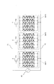
- the presence / absence of defects is determined for the plurality of subarrays SA61, SA62, SA63,... (Defect determination step). For example, a voltage is applied from the AC power supply AC between the first electrode 61 and the second electrode 62 to cause the light emitting diodes D of the subarrays SA61, SA62, SA63,. Whether or not there is.
- the wiring L61 connecting the one end of the sub-array determined to be defective and the first electrode 61 is cut by a laser (separation process).
- the wiring L62 that connects the second electrode 62 to the other end of the subarray that has been determined to be defective may be cut by a laser, or the wiring L61 on both sides of the defective subarray. , L62 may be cut by a laser.
- the occurrence of a light emitting failure due to a short circuit failure can be reduced at a low cost by a step of electrically separating the defective subarray from the first electrode 61 (or the second electrode 62). it can. Therefore, it is possible to realize a light-emitting device with a high yield while suppressing variation in light-emitting characteristics by using a fine bar-shaped light-emitting diode.
- FIG. 13 shows a circuit diagram of a light emitting device according to a seventh embodiment of the present invention.
- the light emitting device of the seventh embodiment has the same configuration as the light emitting device of the third embodiment except for the transistors.
- one end of each of the subarrays SA71, SA72, SA73,... And the first electrode 61 are connected by transistors T71, T72, T73,. ing. Further, the other end of each of the subarrays SA71, SA72, SA73,... Is connected to the second electrode 62.
- the resistance to defects such as open / short of the rod-shaped light-emitting diode D is enhanced by the configuration of the light emitting device of the third embodiment, but the probability that a defective subarray will occur with a certain probability still remains. There is a possibility that the luminous efficiency of the entire light emitting device is lowered. For example, there may be a case where a large current flows through the defective sub-array and a sufficient current is not supplied to the other non-defective sub-arrays.
- the presence or absence of defects is determined for the subarrays SA71, SA72, SA73,... (Defect determination process).
- the transistor is turned off by gate control by a transistor T71 that connects one end of a subarray (for example, SA72 and SA73 in FIG. 13) determined to be defective to the first electrode 61.
- the control circuit of the light emitting device is configured so that an off signal is applied to the gates of the transistors corresponding to the subarrays determined to be defective during the operation of the light emitting device.
- a control device that controls the gate of the transistor may be provided, or a switch circuit that controls the gate of the transistor may be provided.
- a transistor for controlling the power supply of the subarray can be manufactured at low cost by using a TFT (Thin Film Transistor) as the transistor.
- TFT Thin Film Transistor
- FIG. 14 and 15 are views for explaining a method of manufacturing a light emitting device according to the eighth embodiment of the invention.
- a method for manufacturing the light emitting device having the configuration shown in FIG. 1 of the first embodiment will be described.
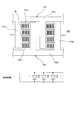
- a first array electrode 101 and a second array electrode 102 are formed on a substrate 100 (array electrode forming step).
- Each of the first array electrode 101 and the second array electrode 102 has base portions 101a and 102a parallel to each other.
- the first array electrode 101 has a plurality of branch portions 101b extending from the base portion 101a toward the second array electrode 102, while the second array electrode 102 has a first portion from the base portion 102a.
- a plurality of branch portions 102 b extending toward the first array electrode 101 and between the branch portions 101 b of the first array electrode 101.
- the first array electrode 101 and the second array electrode 102 are formed between the branch portions 101b and 102b, and have comb-like portions 101c and 102c that are alternately arranged in parallel with each other.
- the rod-shaped light emitting diodes D are connected in parallel between the first array electrode 101 and the second array electrode 102 on the substrate 100 (parallel connection step). That is, a plurality of bar-shaped light emitting diodes D are connected between the comb-shaped portions 101c and 102c of the first array electrode 101 and the second array electrode 102.
- the lower part of FIG. 14 shows an equivalent circuit in a state where the rod-shaped structure light emitting diodes D are connected in parallel.
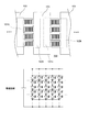
- the light emitting diode parallel circuit in which a plurality of rod-shaped light emitting diodes D are connected in parallel is divided. (Dividing process).
- connection electrode 103 for connecting the light emitting diode parallel circuits in series is formed (series connection step).
- the lower part of FIG. 15 shows an equivalent circuit in a state where a plurality of light emitting diode parallel circuits are connected in series.
- the substrate 100 is an insulating substrate
- the first and second array electrodes 101 and 02 are metal electrodes.
- a metal electrode having a desired electrode shape can be formed on the surface of an insulating substrate using a printing technique.
- a metal film and a photoreceptor film are uniformly laminated on the surface of the insulating substrate, this photoreceptor film is exposed and developed to a desired electrode pattern, and the metal film is etched using the patterned photoreceptor film as a mask.
- a metal electrode can be formed.
- the insulating substrate may be a flexible substrate.
- a metal material for producing the metal electrode gold, silver, copper, iron, tungsten, tungsten nitride, aluminum, tantalum, alloys thereof, and the like can be used.
- the insulating substrate is an insulator such as glass, ceramic, alumina, or resin, or a substrate in which a silicon oxide film is formed on a semiconductor surface such as silicon and the surface is insulative. When a glass substrate is used, it is desirable to form a base insulating film such as a silicon oxide film or a silicon nitride film on the surface.
- the distance between the comb-shaped portions 101c and 102c of the first and second array electrodes 101 and 02 is preferably slightly shorter than the length of the rod-shaped structure light emitting diode D.
- the distance between the comb-shaped portions 101c and 102c is preferably 6 to 9 ⁇ m when the length of the bar-shaped light emitting diode D is 10 ⁇ m.
- IPA isopropyl alcohol
- the solution may be ethylene glycol, propylene glycol, methanol, ethanol, acetone, or a mixture thereof, and liquids such as other organic substances, water, and the like can be used.
- an insulating film of about 10 nm to 30 nm may be coated on the entire surface of the substrate 100 so as to cover the first and second array electrodes 101, 02.
- the thickness of applying the IPA including the bar-shaped light-emitting diode D is such that the bar-shaped light-emitting diode D can be moved in the liquid so that the bar-shaped light-emitting diodes D can be arranged in a parallel connection process. Is the thickness. Therefore, it is not less than the thickness of the rod-shaped structure light emitting diode D, and is, for example, several ⁇ m to several mm. If the applied thickness is too thin, the rod-shaped light emitting diode D is difficult to move, and if it is too thick, the time for drying the liquid becomes long. Preferably, it is 100 ⁇ m to 500 ⁇ m. Further, the number of light emitting diodes is preferably 1 ⁇ 10 4 / cm 3 to 1 ⁇ 10 7 / cm 3 with respect to the amount of IPA.
- a frame (not shown) is formed around the first and second array electrodes 101,02 on which the rod-shaped light emitting diode D is arranged. Then, it is preferable to fill the frame with IPA including the rod-shaped light emitting diode D so as to have a desired thickness. However, when the IPA including the rod-shaped light emitting diode D has viscosity, it can be applied to a desired thickness without requiring a frame.
- the IPA, ethylene glycol, propylene glycol, methanol, ethanol, acetone, a mixture thereof, a liquid made of other organic substances, or a liquid such as water is viscous for the alignment process of the rod-shaped light emitting diode D. Is preferably as low as possible, and it is desirable that it is easily evaporated by heating.
- a potential difference is applied between the first and second array electrodes 101 and 102.
- This potential difference is, for example, a potential difference of 0.5V or 1V. Note that the potential difference is preferably 0.5 V to 5 V, and more preferably about 0.5 V.
- Negative charges are induced on one of the first and second array electrodes 101 and 102, and positive charges are induced on the other of the first and second array electrodes 101 and 102.
- a positive charge is applied to the side of the rod-shaped structure light emitting diode D close to one of the first and second array electrodes 101 and 102.
- the bar-shaped light-emitting diode D has a posture along the electric lines of force generated between the first and second array electrodes 101 and 102, and the charges induced in the bar-shaped light-emitting diodes D are substantially equal. As a result, they are regularly arranged in a fixed direction at almost equal intervals by the repulsive force due to electric charges.
- the surface of the first and second array electrodes 101 and 102 is coated with an insulating film, and the potential difference applied between the first and second array electrodes 101 and 102 is constant (DC). If so, ions having a polarity opposite to the potential of the first and second array electrodes 101 and 102 are induced on the surface of the insulating film coded on the first and second array electrodes 101 and 102 in the solution. The electric field becomes very weak. In such a case, it is preferable to apply an AC voltage between the first and second array electrodes 101 and 102.
- the frequency of the alternating voltage applied between the first and second array electrodes 101 and 102 is preferably 10 Hz to 1 MHz. However, when the frequency of the alternating voltage is less than 10 Hz, the light emitting diode 24 is intense. It can oscillate and disturb the alignment.
- the frequency of the AC voltage applied between the first and second array electrodes 101 and 102 exceeds 1 MHz
- the rod-shaped structure light emitting diode D is adsorbed by the first and second array electrodes 101 and 102.
- the force of the force becomes weak and the arrangement may be disturbed by external disturbances.
- the frequency of the AC voltage it is more preferable that the frequency of the AC voltage be 50 Hz to 1 kHz.
- the waveform of the AC voltage is not limited to a sine wave, but may be any waveform that varies periodically, such as a rectangular wave, a triangular wave, and a sawtooth wave.
- the amplitude of the AC voltage is preferably about 0.5 V as an example.
- the external electric field generated between the first and second array electrodes 101 and 102 generates charges in each of the rod-shaped light emitting diodes D, and the first and second array electrodes 101 are generated by the attractive force of the charges.
- 102 is made to adsorb the rod-shaped structure light emitting diode D, the size of the rod-shaped structure light emitting diode D must be movable in the liquid. Therefore, the allowable value of the size (maximum dimension) of each bar-shaped light emitting diode D varies depending on the application amount (application thickness) of the liquid.
- each rod-shaped light emitting diode D When the liquid application amount is small, the size (maximum dimension) of each rod-shaped light emitting diode D must be nanoscale, but when the liquid application amount is large, the size of each rod-shaped light emitting diode D is large. May be in the micron order.
- the rod-shaped light emitting diode D When the rod-shaped light emitting diode D starts to be arranged for a while, the rod-shaped light emitting diode D is arranged between the first and second array electrodes 101 and 102.
- the rod-shaped structure light emitting diodes D are aligned in a posture perpendicular to the direction in which the first and second arrangement electrodes 101 and 102 extend, and are arranged at substantially equal intervals in the extending direction.
- the electric field concentrates between the first and second array electrodes 101 and 102, and a repulsive force acts between the rod-shaped light emitting diodes D due to the charges induced in the rod-shaped light emitting diodes D. Line up at equal intervals.
- the liquid of the solution is evaporated and dried by heating the substrate 100 or leaving it for a certain period of time.
- the rod-shaped structure light emitting diodes D are arranged and fixed at equal intervals along the lines of electric force between the first array electrode 101 and the second array electrode 102.
- the manufacturing method of the light emitting device it is possible to arrange the rod-shaped light emitting diodes D between the first and second arrangement electrodes 101 and 102 with high controllability and high accuracy.
- a mask having a growth hole is formed on a substrate made of n-type GaN.
- an n-type GaN crystal is grown on the substrate exposed by the growth hole of the mask to form a rod-shaped semiconductor core.
- the n-type GaN has hexagonal crystal growth, and a hexagonal column-shaped semiconductor core can be obtained by growing the n-type GaN in the c-axis direction perpendicular to the substrate surface.
- a semiconductor layer made of p-type GaN is formed on the entire surface of the substrate so as to cover the rod-shaped semiconductor core.
- the region excluding the portion of the semiconductor layer covering the semiconductor core and the mask are removed by lift-off, and the exposed portion is formed by exposing the outer peripheral surface on the substrate side to the substrate side of the rod-shaped semiconductor core.
- the end surface of the semiconductor core opposite to the substrate is covered with a semiconductor layer.
- lift-off is used, but a part of the semiconductor core may be exposed by etching.
- the substrate is vibrated along the plane of the substrate using ultrasonic waves (for example, several tens of kHz) so that the base close to the substrate side of the semiconductor core standing on the substrate is bent. Stress acts on the semiconductor core covered with the semiconductor layer, and the semiconductor core covered with the semiconductor layer is separated from the substrate. Thus, a fine rod-shaped light emitting diode D cut off from the substrate can be manufactured.
- ultrasonic waves for example, several tens of kHz
- FIG. 16 shows a circuit diagram of the light emitting device of the first embodiment.
- a bar-shaped light-emitting diode D having a short circuit is present in the grid array, another bar-shaped light-emitting element connected in parallel is shown.
- the current flowing through the diode D is reduced, and the emission intensity is reduced. If the vertical bar-shaped light-emitting diode D shown in FIG. 16 has a short circuit failure, current concentrates on the bar-shaped light-emitting diode D, and the normal bar-shaped light-emitting diode D indicated by a horizontal line in the same light-emitting diode parallel circuit Luminous intensity decreases.
- a light emitting device including a rod-shaped light emitting diode having a rod-shaped first conductivity type semiconductor core and a cylindrical second conductivity type semiconductor layer surrounded by the semiconductor core
- the rod-shaped structure light emitting diode is not limited to this, and a quantum well layer is provided between the outer peripheral surface of the rod-shaped first conductivity type semiconductor core and the cylindrical second conductivity type semiconductor layer surrounded by the semiconductor core. It may be formed, or may be a conductive layer having a lower resistance than the semiconductor layer so as to cover the semiconductor layer.
- the present invention may be applied to a light emitting device using a rod-shaped structure light emitting diode in which a first conductive type semiconductor layer and a second conductive type semiconductor layer are formed in order so as to cover the outer periphery of the rod-shaped core portion.
- a rod-shaped structure light emitting diode in which the outer periphery of a rod-shaped core portion made of SiC is covered with a semiconductor layer made of n-type GaN and a semiconductor layer made of p-type GaN may be used.
- a semiconductor core is composed of a rod-shaped core portion made of SiC and a semiconductor layer made of n-type GaN.
- a semiconductor using GaN as a base material is used for the substrate, the semiconductor core, and the semiconductor layer.
- a semiconductor may be used.
- the substrate and the semiconductor core are n-type and the semiconductor layer is p-type, a rod-shaped structure light emitting diode having a reverse conductivity type may be used.
- the rod-shaped structure light emitting diode having a semiconductor core having a hexagonal column in the cross section has been described, the present invention is not limited to this, and the cross section may be a circular or elliptical rod shape, or the cross section may be another polygonal rod shape such as a triangle.
- a rod-shaped structure light emitting diode having the above semiconductor core can also be manufactured by the same manufacturing method as described above.
- the array yield can be improved by setting the ratio of the length of the rod-shaped light emitting diode to the diameter of the semiconductor core to be 5 or more and 200 or less.
- the diameter of the semiconductor core of the rod-shaped light emitting diode is preferably 500 nm or more and 100 ⁇ m or less, and the variation in the diameter of the semiconductor core is suppressed as compared with the rod-shaped light emitting diode having a diameter of several tens to several hundreds of nm.
- variation in light emitting area that is, light emission characteristics can be reduced, and yield can be improved.
- the semiconductor core is crystal-grown using the MOCVD apparatus.
- the semiconductor core may be formed using another crystal growth apparatus such as an MBE (molecular beam epitaxial) apparatus. Good.
- MBE molecular beam epitaxial
- the semiconductor core may be crystal-grown from the metal seed by arranging a metal species on the substrate.
- the semiconductor core covered with the semiconductor layer is separated from the substrate using ultrasonic waves.
- the present invention is not limited thereto, and the semiconductor core is mechanically removed from the substrate using a cutting tool. May be separated. In this case, a plurality of fine rod-shaped light emitting elements provided on the substrate can be separated in a short time by a simple method.
- the light emitting device of the present invention for a backlight of a liquid crystal display device or the like, it is possible to suppress a variation in light emission characteristics and realize a backlight with a high yield.
- the light-emitting device of the present invention as a lighting device, it is possible to realize a lighting device with high yield while suppressing variations in light emission characteristics.
- the light-emitting device of the present invention for a display device, it is possible to realize a display device with high yield while suppressing variations in light-emitting characteristics.
- the light-emitting device of the present invention is used for pixels arranged in a matrix.
- the light emitting device of the present invention is A light emitting diode series circuit in which rod-shaped structure light emitting diodes are connected in series is connected in parallel, and a lattice array in which the rod-shaped structure light emitting diodes are arranged in a grid pattern; A first electrode connected to one end of the grid array; A second electrode connected to the other end of the grid array, All of the rod-shaped structure light emitting diodes are arranged in a forward direction toward the first electrode side or the second electrode side,
- the rod-shaped structure light emitting diode includes a rod-shaped first-conductivity-type semiconductor core having a length to diameter ratio of 5 to 200 and a diameter of 500 nm to 100 ⁇ m, and a cylinder surrounding the semiconductor core And a second conductive type semiconductor layer.
- the diameter of the semiconductor core is set to 500 nm or more and 100 ⁇ m or less, variation in the diameter of the semiconductor core can be suppressed as compared with the semiconductor core having a diameter of several tens to several hundreds of nm. Therefore, in a light-emitting device using a fine rod-shaped light-emitting diode, a light-emitting device with high yield can be realized while suppressing variations in light emission characteristics.
- the grid array has a plurality of subarrays in which a plurality of the light emitting diode series circuits are connected in parallel, The plurality of subarrays are connected in series between the first electrode and the second electrode.
- any one of the above light emitting devices is provided.
- SYMBOLS 1 Semiconductor core 2 ... Semiconductor layer 11, 21, 31, 41, 61, 71 ... 1st electrode 12, 22, 32, 42, 62, 72 ... 2nd electrode 40,100 ... Board
Landscapes
- Physics & Mathematics (AREA)
- Nonlinear Science (AREA)
- Mathematical Physics (AREA)
- Chemical & Material Sciences (AREA)
- Crystallography & Structural Chemistry (AREA)
- General Physics & Mathematics (AREA)
- Optics & Photonics (AREA)
- Led Devices (AREA)
- Non-Portable Lighting Devices Or Systems Thereof (AREA)
Abstract
棒状構造発光ダイオード(D)が並列に接続された発光ダイオード並列回路が複数個直列に接続されて、棒状構造発光ダイオード(D)が格子状に配列された格子状アレイ(A1)と、格子状アレイ(A1)の一端に接続された第1の電極(11)と、格子状アレイの他端に接続された第2の電極(12)とを備える。上記棒状構造発光ダイオード(D)は、径に対する長さの比が5以上かつ200以下であり、かつ、径が500nm以上かつ100μm以下である棒状のn型GaNからなる半導体コアと、その半導体コアの囲む筒状のp型GaNからなる半導体層とを有する。これにより、微細な棒状構造発光ダイオードを用いた発光装置において、発光特性のばらつきを抑えて、歩留まりのよい発光装置を提供する。
Description
この発明は、発光装置、発光装置の製造方法、照明装置、バックライトおよび表示装置に関する。
従来、発光装置としては、直列に接続された発光ダイオードが複数個並列に接続されたものがある(例えば、特開2002-173028号公報(特許文献1)参照)。
このような構成の発光装置において、微細な棒状構造を有する発光ダイオードを適用した場合、配列不良などに起因するオープン不良が多数発生することによって、製造歩留りの大きな低下を招く。
また、上記微細な棒状構造を有する発光ダイオードを用いた構造では、順方向を揃えて配列する極性制御が容易でないために直列接続では電流パスが形成できず、交流動作を実現できない。
図18に示す直列型の発光装置の場合、定電流駆動により発光ダイオードの特性ばらつきに対して強いが、オープンモードの不良に対して弱いという問題がある(1つの発光ダイオード不良が発生すると電流パスが切れる)。
また、図19に示す並列型の発光装置の場合、オープンモードの不良に対して強いが、低電圧駆動により素子の特性ばらつきに対して弱く、さらに、ショートモードの不良に対して弱いという問題がある(ショートモードの発光ダイオードに電流が流れ続けると、他の発光ダイオードに電流が流れない)。
さらに、図20に示す直並列型の発光装置の場合、図18,図19に示す発光装置の両方の長所と短所を共に有する。
発光ダイオードを用いた一般的な発光装置では、特性ばらつきに強い直列型、もしくは、直列型を並列に並べた直並列型を採用している事例が多く、並列型は特性ばらつきおよび駆動電圧の面から採用されている事例はほとんど見られない。
このように、微細な棒状構造発光ダイオードを用いた発光装置では、発光特性のばらつきを抑えることができず、歩留まりが悪いという問題がある。
そこで、この発明の課題は、微細な棒状構造発光ダイオードを用いた発光装置において、発光特性のばらつきを抑えて、歩留まりのよい発光装置および発光装置の製造方法を提供することにある。
また、この発明のもう一つの課題は、発光特性のばらつきを抑えて、歩留まりのよい照明装置、バックライトおよび表示装置を提供することにある。
上記課題を解決するため、この発明の発光装置は、
棒状構造発光ダイオードが並列に接続された発光ダイオード並列回路が、複数個直列に接続されて、上記棒状構造発光ダイオードが格子状に配列された格子状アレイと、
上記格子状アレイの一端に接続された第1の電極と、
上記格子状アレイの他端に接続された第2の電極と
を備え、
上記棒状構造発光ダイオードは、径に対する長さの比が5以上かつ200以下であり、かつ、径が500nm以上かつ100μm以下である棒状の第1導電型の半導体コアと、その半導体コアの囲む筒状の第2導電型の半導体層とを有することを特徴とする。
棒状構造発光ダイオードが並列に接続された発光ダイオード並列回路が、複数個直列に接続されて、上記棒状構造発光ダイオードが格子状に配列された格子状アレイと、
上記格子状アレイの一端に接続された第1の電極と、
上記格子状アレイの他端に接続された第2の電極と
を備え、
上記棒状構造発光ダイオードは、径に対する長さの比が5以上かつ200以下であり、かつ、径が500nm以上かつ100μm以下である棒状の第1導電型の半導体コアと、その半導体コアの囲む筒状の第2導電型の半導体層とを有することを特徴とする。
上記構成によれば、棒状構造発光ダイオードが並列に接続された発光ダイオード並列回路が、複数個直列に接続されて、上記棒状構造発光ダイオードが格子状に配列された格子状アレイを用いることによって、棒状構造発光ダイオードの配列不良などに起因するオープン不良に対する耐性が高まり、製造歩留りを高めることができる。また、棒状構造発光ダイオードの半導体コアの径に対する長さの比を5以上かつ200以下とすることにより、配列歩留まりを向上できる。さらに、半導体コアの径を500nm以上かつ100μm以下とすることによって、径が数10nm~数100nm程度のものに比べて、半導体コアの径のばらつきを抑えることができる。したがって、微細な棒状構造発光ダイオードを用いた発光装置において、発光特性のばらつきを抑えて、歩留まりのよい発光装置を実現できる。
また、一実施形態の発光装置では、
上記格子状アレイは、上記発光ダイオード並列回路が複数個直列に接続されたサブアレイを複数有し、
上記複数のサブアレイが上記第1の電極と上記第2の電極との間に並列に接続されている。
上記格子状アレイは、上記発光ダイオード並列回路が複数個直列に接続されたサブアレイを複数有し、
上記複数のサブアレイが上記第1の電極と上記第2の電極との間に並列に接続されている。
上記実施形態によれば、複数のサブアレイを第1の電極と第2の電極との間に並列に接続することによって、ショートした棒状構造発光ダイオードの直列接続パスが発生する確率を低減できる。したがって、棒状構造発光ダイオードのショート不良に起因する発光不良の発生を低減できる。
また、一実施形態の発光装置では、
上記複数のサブアレイは、上記棒状構造発光ダイオードの全てが上記第1の電極側または上記第2の電極側に向かって順方向となるように配列され、
上記各サブアレイの上記発光ダイオード並列回路における上記棒状構造発光ダイオードの数が35以上である。
上記複数のサブアレイは、上記棒状構造発光ダイオードの全てが上記第1の電極側または上記第2の電極側に向かって順方向となるように配列され、
上記各サブアレイの上記発光ダイオード並列回路における上記棒状構造発光ダイオードの数が35以上である。
上記実施形態によれば、棒状構造発光ダイオードのショート不良に起因する電圧降下を抑制することが可能となり、発光不良の発生を低減することができる。
また、一実施形態の発光装置では、
上記複数のサブアレイは、上記第1の電極側に向かって順方向となるように接続された上記棒状構造発光ダイオードと、上記第2の電極側に向かって順方向となるように接続された上記棒状構造発光ダイオードとがランダムに配列され、
上記各サブアレイの上記発光ダイオード並列回路における上記棒状構造発光ダイオードの数は70以上である。
上記複数のサブアレイは、上記第1の電極側に向かって順方向となるように接続された上記棒状構造発光ダイオードと、上記第2の電極側に向かって順方向となるように接続された上記棒状構造発光ダイオードとがランダムに配列され、
上記各サブアレイの上記発光ダイオード並列回路における上記棒状構造発光ダイオードの数は70以上である。
上記実施形態によれば、棒状構造発光ダイオードのショート不良に起因する電圧降下を抑制することが可能となり、発光不良の発生を低減することができる。
また、一実施形態の発光装置では、
上記複数のサブアレイは、複数のサブアレイグループに分類され、
上記サブアレイグループ毎に、電源電圧を供給する電源部を備えた。
上記複数のサブアレイは、複数のサブアレイグループに分類され、
上記サブアレイグループ毎に、電源電圧を供給する電源部を備えた。
上記実施形態によれば、1つのサブアレイグループの棒状構造発光ダイオードのショート不良が発生しても、他のサブアレイグループは電源部が異なり、供給される電源電圧への影響が少ないので、発光ばらつきを低減できる。
また、一実施形態の発光装置では、
上記格子状アレイは、上記第1の電極側に向かって順方向となるように接続された上記棒状構造発光ダイオードと、上記第2の電極側に向かって順方向となるように接続された上記棒状構造発光ダイオードとがランダムに配列されている。
上記格子状アレイは、上記第1の電極側に向かって順方向となるように接続された上記棒状構造発光ダイオードと、上記第2の電極側に向かって順方向となるように接続された上記棒状構造発光ダイオードとがランダムに配列されている。
上記実施形態によれば、第1の電極と第2の電極との間に交流電圧を印加して、交流動作による駆動を実現することができる。また、棒状構造発光ダイオードを同一方向に向かって順方向に配列する必要がないので、製造プロセスが簡略化されて製造コストを低減できる。
また、この発光装置の製造方法では、
棒状構造発光ダイオードが並列に接続された発光ダイオード並列回路が、複数個直列に接続されて、上記棒状構造発光ダイオードが格子状に配列された格子状アレイと、上記格子状アレイの一端に接続された第1の電極と、上記格子状アレイの他端に接続された第2の電極とを備え、上記棒状構造発光ダイオードは、径に対する長さの比が5以上かつ200以下であり、かつ、径が500nm以上かつ100μm以下である棒状の第1導電型の半導体コアと、その半導体コアの囲む筒状の第2導電型の半導体層とを有する発光装置を製造する発光装置の製造方法であって、
上記格子状アレイは、上記発光ダイオード並列回路が複数個直列に接続されたサブアレイを複数有し、
上記複数のサブアレイに対して不良の有無を判別する不良判別工程と、
上記複数のサブアレイのうち、上記不良判別工程で不良と判別されたサブアレイと上記第1の電極との接続、または、上記不良判別工程で不良と判別されたサブアレイと上記第2の電極との接続の少なくとも一方を切り離す切り離し工程と
を含むことを特徴とする。
棒状構造発光ダイオードが並列に接続された発光ダイオード並列回路が、複数個直列に接続されて、上記棒状構造発光ダイオードが格子状に配列された格子状アレイと、上記格子状アレイの一端に接続された第1の電極と、上記格子状アレイの他端に接続された第2の電極とを備え、上記棒状構造発光ダイオードは、径に対する長さの比が5以上かつ200以下であり、かつ、径が500nm以上かつ100μm以下である棒状の第1導電型の半導体コアと、その半導体コアの囲む筒状の第2導電型の半導体層とを有する発光装置を製造する発光装置の製造方法であって、
上記格子状アレイは、上記発光ダイオード並列回路が複数個直列に接続されたサブアレイを複数有し、
上記複数のサブアレイに対して不良の有無を判別する不良判別工程と、
上記複数のサブアレイのうち、上記不良判別工程で不良と判別されたサブアレイと上記第1の電極との接続、または、上記不良判別工程で不良と判別されたサブアレイと上記第2の電極との接続の少なくとも一方を切り離す切り離し工程と
を含むことを特徴とする。
上記構成によれば、棒状構造発光ダイオードのショート不良に起因する発光不良の発生を低コストで低減することができ、棒状構造発光ダイオードの配列不良などに起因するオープン不良に対する耐性が高まることと相俟って、製造歩留りを高めることができる。したがって、半導体コアの径に対する長さの比が5以上かつ200以下であり、かつ、半導体コアの径が500nm以上かつ100μm以下である微細な棒状構造発光ダイオードを用いて、発光特性のばらつきを抑えつつ、歩留まりのよい発光装置を実現できる。
また、一実施形態の発光装置の製造方法では、
上記切り離し工程において、上記不良と判別されたサブアレイの一端と上記第1の電極とを接続する配線、または、上記不良と判別されたサブアレイの他端と上記第2の電極とを接続する配線の少なくとも一方をレーザーにより切断する。
上記切り離し工程において、上記不良と判別されたサブアレイの一端と上記第1の電極とを接続する配線、または、上記不良と判別されたサブアレイの他端と上記第2の電極とを接続する配線の少なくとも一方をレーザーにより切断する。
上記実施形態によれば、棒状構造発光ダイオードのショート不良に起因する発光不良の発生を正確に除去することができる。
また、一実施形態の発光装置の製造方法では、
上記不良判別工程の前に、上記サブアレイ毎に、上記サブアレイの一端と上記第1の電極との間、または、そのサブアレイの他端と上記第2の電極との間の少なくとも一方に接続されたトランジスタを形成するトランジスタ形成工程を含む。
上記不良判別工程の前に、上記サブアレイ毎に、上記サブアレイの一端と上記第1の電極との間、または、そのサブアレイの他端と上記第2の電極との間の少なくとも一方に接続されたトランジスタを形成するトランジスタ形成工程を含む。
上記実施形態によれば、上記切り離し工程において、上記不良判別工程において不良と判別されたサブアレイの一端と上記第1の電極との間、または、上記不良と判別されたサブアレイの他端と上記第2の電極との間の少なくとも一方に接続されたトランジスタを、ゲート制御により発光動作時にオフ状態にする。これによって、棒状構造発光ダイオードのショート不良に起因する発光不良の発生を正確に除去することができる。
また、一実施形態の発光装置の製造方法では、
上記トランジスタは、薄膜トランジスタである。
上記トランジスタは、薄膜トランジスタである。
上記実施形態によれば、トランジスタを安価に製造することができる。
また、一実施形態の発光装置の製造方法では、
上記不良判別工程前に、基板上に第1の配列用電極と第2の配列用電極とを形成する配列用電極形成工程と、
上記基板上の第1の配列用電極と第2の配列用電極との間に、上記棒状構造発光ダイオードを並列に接続する並列接続工程と、
上記並列接続工程の後に、上記第1の配列用電極または上記第2の配列用電極の少なくとも一方の電極の一部を除去することにより、上記棒状構造発光ダイオードが並列に複数個接続された発光ダイオード並列回路毎に分割する分割工程と、
上記分割工程の後、上記発光ダイオード並列回路を直列に接続するための接続用電極を形成する直列接続工程と
を含む。
上記不良判別工程前に、基板上に第1の配列用電極と第2の配列用電極とを形成する配列用電極形成工程と、
上記基板上の第1の配列用電極と第2の配列用電極との間に、上記棒状構造発光ダイオードを並列に接続する並列接続工程と、
上記並列接続工程の後に、上記第1の配列用電極または上記第2の配列用電極の少なくとも一方の電極の一部を除去することにより、上記棒状構造発光ダイオードが並列に複数個接続された発光ダイオード並列回路毎に分割する分割工程と、
上記分割工程の後、上記発光ダイオード並列回路を直列に接続するための接続用電極を形成する直列接続工程と
を含む。
上記実施形態によれば、棒状構造発光ダイオードのショート不良に起因する発光不良の発生を低コストで低減できる。
また、一実施形態の発光装置の製造方法では、
上記第1の電極と上記第2の電極との間に電圧を印加して、上記格子状アレイに対して、予め設定された電流を予め設定された時間流すことによって、上記格子状アレイの上記棒状構造発光ダイオードに対してスクリーニングを行うスクリーニング工程を含む。
上記第1の電極と上記第2の電極との間に電圧を印加して、上記格子状アレイに対して、予め設定された電流を予め設定された時間流すことによって、上記格子状アレイの上記棒状構造発光ダイオードに対してスクリーニングを行うスクリーニング工程を含む。
上記実施形態によれば、棒状構造発光ダイオードのショート不良に起因する発光不良の発生を低コストで低減することができる。
また、一実施形態の発光装置の製造方法では、
上記配列工程の後かつ上記分割工程の前に、上記第1の配列用電極と上記第2の配列用電極との間に予め設定された電圧を印加することによって、上記棒状構造発光ダイオードに対してスクリーニングを行うスクリーニング工程を含む。
上記配列工程の後かつ上記分割工程の前に、上記第1の配列用電極と上記第2の配列用電極との間に予め設定された電圧を印加することによって、上記棒状構造発光ダイオードに対してスクリーニングを行うスクリーニング工程を含む。
上記実施形態によれば、並列接続された全ての棒状構造発光ダイオードに実質的に同じ電圧が印加され、特性ばらつきに応じた電流が流れることにより、棒状構造発光ダイオードのショート不良に起因する発光不良の発生をより効率的に低減することができる。
また、この発明の照明装置では、
上記のいずれか1つの発光装置を備えたことを特徴とする。
上記のいずれか1つの発光装置を備えたことを特徴とする。
上記構成によれば、発光特性のばらつきを抑えて、歩留まりのよい照明装置を実現できる。
また、この発明のバックライトでは、
上記のいずれか1つの発光装置を備えたことを特徴とする。
上記のいずれか1つの発光装置を備えたことを特徴とする。
上記構成によれば、発光特性のばらつきを抑えて、歩留まりのよいバックライト実現できる。
また、この発明の表示装置では、
上記のいずれか1つの発光装置を備えたことを特徴とする。
上記のいずれか1つの発光装置を備えたことを特徴とする。
上記構成によれば、発光特性のばらつきを抑えて、歩留まりのよい表示装置を実現できる。
以上より明らかなように、この発明の発光装置および発光装置の製造方法によれば、微細な棒状構造発光ダイオードを用いた発光装置において、発光特性のばらつきを抑えて、歩留まりのよい発光装置および発光装置の製造方法を実現することができる。
また、この発明の照明装置、バックライトおよび表示装置によれば、発光特性のばらつきを抑えて、歩留まりのよい照明装置、バックライトおよび表示装置を実現することができる。
以下、この発明の発光装置、発光装置の製造方法、照明装置、バックライトおよび表示装置を図示の実施の形態により詳細に説明する。
〔第1実施形態〕
図1Aはこの発明の第1実施形態の発光装置の回路図を示している。この第1実施形態の発光装置は、図1Aに示すように、複数の棒状構造発光ダイオードDが格子状に配列された格子状アレイA1を備えている。この格子状アレイA1では、棒状構造発光ダイオードDが並列に接続された発光ダイオード並列回路を複数個直列に接続することにより、複数の棒状構造発光ダイオードDを格子状に配列している。
図1Aはこの発明の第1実施形態の発光装置の回路図を示している。この第1実施形態の発光装置は、図1Aに示すように、複数の棒状構造発光ダイオードDが格子状に配列された格子状アレイA1を備えている。この格子状アレイA1では、棒状構造発光ダイオードDが並列に接続された発光ダイオード並列回路を複数個直列に接続することにより、複数の棒状構造発光ダイオードDを格子状に配列している。
そして、この発光装置は、格子状アレイA1の一端に接続された第1の電極11と、格子状アレイA1の他端に接続された第2の電極12とを備えている。上記第1の電極11に直流電源DCの正極側出力端子が接続され、第2の電極12に直流電源DCの負極側出力端子が接続されている。
また、上記格子状アレイA1は、棒状構造発光ダイオードDの全てが第2の電極12側に向かって順方向となるように配列されている。すなわち、棒状構造発光ダイオードDのカソード側が第2の電極12側に向き、棒状構造発光ダイオードDのアノード側が第1の電極11側に向いている。
なお、図1Bに示すように、N個(Nは2以上の整数)の棒状構造発光ダイオードDが直列に接続された発光ダイオード直列回路を複数個並列に接続したサブアレイSA101を複数直列に接続して、複数の棒状構造発光ダイオードDを格子状に配列してもよい。この場合、棒状構造発光ダイオードDのショート不良が多い場合に有効である。
図1Bでは、N個(Nは2以上の整数)の棒状構造発光ダイオードDが直列に接続された発光ダイオード直列回路を複数個並列に接続したサブアレイSA101を複数直列に接続していたが、ダイオード直列回路の直列接続された棒状構造発光ダイオードDの数は、同じである必要はない。例えば、図1Cに示すように、N個(Nは2以上の整数)の棒状構造発光ダイオードDが直列に接続された発光ダイオード直列回路を複数個並列に接続したサブアレイSA101と、M個(Mは1または3以上の整数)の棒状構造発光ダイオードDが直列に接続された発光ダイオード直列回路を複数個並列に接続したサブアレイSA102とを直列に接続してもよい。このような構成では、棒状構造発光ダイオードDのオープン不良やショート不良の確率に配列場所依存がある場合、発光ダイオード直列回路の直列接続する棒状構造発光ダイオードDの数を配列場所により変化させることにより、歩留まりを向上できる。
図2はこの発光装置の棒状構造発光ダイオードDの側面模式図を示している。
図2に示すように、棒状構造発光ダイオードDの形状は、断面略六角形のn型GaNからなる半導体コア1と、その半導体コア1の囲む筒状のp型GaNからなる半導体層2とを有している。上記半導体コア1は、径に対する長さの比を5以上かつ200以下とすると共に、径を500nm以上かつ100μm以下とすることによって、半導体コア1の径のばらつきを抑えることができる。
上記構成の発光装置によれば、図1Aに示すように、直流電源DCの正極側出力端子から第1の電極11を介して格子状アレイA1の各棒状構造発光ダイオードDに流れて、第2の電極12を介して直流電源DCの負極側出力端子に戻る。これにより、各棒状構造発光ダイオードDが発光する。
そして、例えば、格子状アレイA1の各棒状構造発光ダイオードDのうちの1つにオープン不良が発生しても、他の棒状構造発光ダイオードDで電流パスが存在するので、光量が大きく減ることがない。また、格子状アレイA1の各棒状構造発光ダイオードDのうちの1つにショート不良が発生しても、そのショート不良の棒状構造発光ダイオードDを含む発光ダイオード並列回路の棒状構造発光ダイオードDのみが影響を受けるだけで、他の発光ダイオード並列回路で光量が減ることはない。
したがって、この第1実施形態の発光装置では、発光特性のばらつきを抑えて、歩留まりのよい発光装置を実現することができる。
このような棒状構造発光ダイオードDは、基板上に垂直に成長させた棒状構造発光ダイオードを刈り取り、改めて基板上に配列させることによって、従来法よりも低コストで発光装置を製造することができ、製造コストを削減することができる。
また、刈り取った棒状構造発光ダイオードDを改めて基板上に配列させるため、配列不良に起因するオープン不良(非導通モードの不良)が従来法よりも多数発生するが、図1Aに示す回路構成とすることによって、オープン不良に対する耐性が高まり、製造歩留りを高めることができる。
〔第2実施形態〕
図3はこの発明の第2実施形態の発光装置の回路図を示している。この第2実施形態の発光装置は、棒状構造発光ダイオードDの配列と電源を除いて第1実施形態の発光装置と同一の構成をしている。
図3はこの発明の第2実施形態の発光装置の回路図を示している。この第2実施形態の発光装置は、棒状構造発光ダイオードDの配列と電源を除いて第1実施形態の発光装置と同一の構成をしている。
この第2実施形態の発光装置は、図3に示すように、複数の棒状構造発光ダイオードDが格子状に配列された格子状アレイA2を備えている。この格子状アレイA2では、棒状構造発光ダイオードDが並列に接続された発光ダイオード並列回路を複数個直列に接続することによって、複数の棒状構造発光ダイオードDを格子状に配列している。
そして、この発光装置は、格子状アレイA2の一端に接続された第1の電極21と、格子状アレイA2の他端に接続された第2の電極22とを備えている。上記第1の電極21に交流電源ACの一方の出力端子が接続され、第2の電極22に交流電源ACの他方の出力端子が接続されている。
また、上記格子状アレイA2は、第1の電極21側に向かって順方向となるように接続された上記棒状構造発光ダイオードDと、第2の電極22側に向かって順方向となるように接続された棒状構造発光ダイオードDとがランダムに配列されている。
上記構成の発光装置によれば、交流電源ACから第1の電極21,第2の電極22を介して格子状アレイA1の各棒状構造発光ダイオードDに交流電流が流れる。これにより、各棒状構造発光ダイオードDが発光する。
そして、例えば、格子状アレイA2の各棒状構造発光ダイオードDのうちの1つにオープン不良が発生しても、他の順方向が同一の棒状構造発光ダイオードDで電流パスが存在するので、光量が大きく減ることがない。また、格子状アレイA2の各棒状構造発光ダイオードDのうちの1つにショート不良が発生しても、そのショート不良の棒状構造発光ダイオードDを含む発光ダイオード並列回路の棒状構造発光ダイオードDのうち、順方向が同一のもののみが影響を受けるだけで、他の発光ダイオード並列回路で光量が減ることはない。
したがって、この第2実施形態の発光装置では、発光特性のばらつきを抑えて、歩留まりのよい発光装置を実現することができる。
上記第2実施形態の発光装置は、第1実施形態の発光装置と同様の効果を有する。また、交流動作では棒状構造発光ダイオードDを配列するときに極性制御を行う必要がなく、低コストで回路動作を実現することができる。
また、棒状構造発光ダイオードDの極性がランダムに異なるため、従来の直列に接続した構成では、実質的に回路動作が不可能であるのに対して、この第2実施形態の発光装置では、交流動作による駆動を実現することができ、棒状構造発光ダイオードを同一方向に向かって順方向に配列する必要がないので、製造プロセスが簡略化されて製造コストを低減することができる。
〔第3実施形態〕
図4はこの発明の第3実施形態の発光装置の回路図を示している。この第3実施形態の発光装置は、棒状構造発光ダイオードDの配列を除いて第2実施形態の発光装置と同一の構成をしている。
図4はこの発明の第3実施形態の発光装置の回路図を示している。この第3実施形態の発光装置は、棒状構造発光ダイオードDの配列を除いて第2実施形態の発光装置と同一の構成をしている。
この第3実施形態の発光装置は、図4に示すように、棒状構造発光ダイオードDが格子状に形成されたサブアレイSA1,SA2,SA3,…を有している。複数のサブアレイSA1,SA2,SA3,…で格子状アレイを構成している。上記サブアレイSA1,SA2,SA3,…の夫々では、棒状構造発光ダイオードDが並列に接続された発光ダイオード並列回路を複数個直列に接続することによって、複数の棒状構造発光ダイオードDを格子状に配列している。
上記複数のサブアレイSA1,SA2,SA3,…を第1の電極31と第2の電極32との間に並列に接続している。そして、上記第1の電極31に交流電源ACの一方の出力端子が接続され、第2の電極32に交流電源ACの他方の出力端子が接続されている。
また、サブアレイSA1,SA2,SA3,…は、第1の電極31側に向かって順方向となるように接続された棒状構造発光ダイオードDと、第2の電極32側に向かって順方向となるように接続された棒状構造発光ダイオードDとがランダムに配列されている。
上記構成の発光装置によれば、交流電源ACから第1の電極31,第2の電極32を介してサブアレイSA1,SA2,SA3,…の各棒状構造発光ダイオードDに交流電流が流れる。これにより、各棒状構造発光ダイオードDが発光する。
上記第3実施形態の発光装置は、第2実施形態の発光装置と同様の効果を有する。
この第3実施形態の発光装置では、複数のサブアレイSA1,SA2,SA3,…を備え、各サブアレイSA1,SA2,SA3,…を並列に接続することによって、ショートした棒状構造発光ダイオードDの直列接続パスが発生する確率を低減できるので、棒状構造発光ダイオードDのショート不良に起因する発光不良の発生を低減することができる。
これに対して、上記第1,第2実施形態の発光装置では、棒状構造発光ダイオードDのオープン不良に対する耐性は強いが、発光ダイオード並列回路における棒状構造発光ダイオードDの並列数を上げた場合、棒状構造発光ダイオードDのショート不良(短絡モードの不良)に起因する発光不良の可能性が高まる。すなわち、ショート不良の棒状構造発光ダイオードDの直列接続パスが発生して、格子状アレイ内の正常な棒状構造発光ダイオードDに十分な電流が流れない可能性がある。
〔第4実施形態〕
図5はこの発明の第4実施形態の発光装置の回路図を示している。この第4実施形態の発光装置は、棒状構造発光ダイオードDの配列および電源を除いて第3実施形態の発光装置と同一の構成をしている。この第4実施形態の発光装置は、複数のサブアレイSA11,SA12,SA13,…は、棒状構造発光ダイオードDの全てが第2の電極12側に向かって順方向となるように配列されている点が第3実施形態の発光装置と異なる。
図5はこの発明の第4実施形態の発光装置の回路図を示している。この第4実施形態の発光装置は、棒状構造発光ダイオードDの配列および電源を除いて第3実施形態の発光装置と同一の構成をしている。この第4実施形態の発光装置は、複数のサブアレイSA11,SA12,SA13,…は、棒状構造発光ダイオードDの全てが第2の電極12側に向かって順方向となるように配列されている点が第3実施形態の発光装置と異なる。
この第3実施形態の発光装置は、図5に示すように、棒状構造発光ダイオードDが格子状に形成されたサブアレイSA11,SA12,SA13,…を有している。複数のサブアレイSA11,SA12,SA13,…で格子状アレイを構成している。上記サブアレイSA11,SA12,SA13,…の夫々では、棒状構造発光ダイオードDが並列に接続された発光ダイオード並列回路を複数個直列に接続することによって、複数の棒状構造発光ダイオードDを格子状に配列している。
上記複数のサブアレイSA11,SA12,SA13,…を第1の電極41と第2の電極42との間に並列に接続している。そして、上記第1の電極41に直流電源DCの正極側出力端子が接続され、第2の電極42に直流電源DCの負極側出力端子が接続されている。
また、上記サブアレイSA11,SA12,SA13,…は、複数の棒状構造発光ダイオードDの全てが第2の電極42側に向かって順方向となるように配列されている。すなわち、棒状構造発光ダイオードDのカソード側が第2の電極42側に向き、棒状構造発光ダイオードDのアノード側が第1の電極41側に向いている。
上記構成の発光装置によれば、直流電源DCの正極側出力端子から第1の電極41を介してサブアレイSA1,SA2,SA3,…の各棒状構造発光ダイオードDに流れて、第2の電極42を介して直流電源DCの負極側出力端子に戻る。これにより、各棒状構造発光ダイオードDが発光する。
上記第4実施形態の発光装置は、第1実施形態の発光装置と同様の効果を有する。
また、図6は上記発光装置の要部の断面図を示しており、基板40上に形成された第1の電極41および第2の電極42に跨るように、棒状構造発光ダイオードDが基板40の実装面に対して平行に載置されている。そして、棒状構造発光ダイオードDの一端(アノード)と第1の電極41とを、導電性接着剤などの金属インクからなる接着部43により電気的に接続し、棒状構造発光ダイオードDの他端に露出した半導体コア1の露出部分(カソード)と第2の電極42とを、導電性接着剤などの金属インクからなる接着部44により電気的に接続している。なお、図6では、半導体層2の外周を、半導体層2よりも抵抗の低い導電層3で覆っている。
このような実装形態の棒状構造発光ダイオードDでは、ショート不良の一例として第1の電極41側の半導体コア1と半導体層2との間でショートが発生する場合がある(図6に示す領域S)。
図7は上記発光装置の並列素子数に対する相対光量の関係を示しており、サブアレイ数×並列素子数=700に固定して、相対光量(不良率0%のときの光量に対する比)を測定している。詳しくは、棒状構造発光ダイオードDのショートモードの不良率0.01%、0.05%、0.1%の場合の夫々で、並列素子数に対する相対光量の関係を測定した。
このように、サブアレイ数×並列素子数=700に固定し、サブアレイ数の最適化を行った結果、図7から明らかなように、サブアレイ数を20とし、並列素子数を35以上とすることで、棒状構造発光ダイオードDのショート不良による他の正常な素子(発光ダイオード並列回路内)への影響を少なくできる。すなわち、並列に接続された棒状構造発光ダイオードDが多い図8に示す発光ダイオード並列回路は、並列に接続された棒状構造発光ダイオードDが少ない図9に示す発光ダイオード並列回路よりも、棒状構造発光ダイオードDのショート不良による発光ダイオード並列回路の両端の電圧降下が小さい。このような効果は、並列に接続された正常な棒状構造発光ダイオードDとショート不良の棒状構造発光ダイオードDとの抵抗バランスから得られるものであるため、直列段数による影響は少ない。
このように、複数の棒状構造発光ダイオードDの全てが同じ向きに配列された各サブアレイにおいて、発光ダイオード並列回路の棒状構造発光ダイオードDの並列素子数を35以上とすることによって、棒状構造発光ダイオードDのショート不良に起因する電圧降下を抑制することが可能となり、発光不良の発生を低減することができる。
なお、図4に示す第3実施形態の発光装置の構成において、同様の測定をした結果を図10に示しており、サブアレイ数×並列素子数=1,400に固定し、サブアレイ数の最適化を行った。この場合、図10から明らかなように、サブアレイ数を20とし、並列素子数を70以上とすることで、棒状構造発光ダイオードDのショート不良による他の正常な素子(発光ダイオード並列回路内)への影響が少ない。このような効果は、この第4実施形態の発光装置の構成のときと同様に、並列に接続された正常な棒状構造発光ダイオードDとショート不良の棒状構造発光ダイオードDとの抵抗バランスから得られるものであるため、直列段数による影響は少ない。
このように、複数の棒状構造発光ダイオードDの向きがランダムな各サブアレイにおいて、発光ダイオード並列回路の棒状構造発光ダイオードDの並列素子数を70以上とすることによって、棒状構造発光ダイオードDのショート不良に起因する電圧降下を抑制することが可能となり、発光不良の発生を低減することができる。
〔第5実施形態〕
図11Aはこの発明の第5実施形態の発光装置の回路図を示している。この第5実施形態の発光装置は、図11Aに示すように、電源ブロック50と、電源ブロック50から電源電圧が供給されたサブアレイSA51,SA52,SA53,SA54,…とを備えている。この電源ブロック50は、メイン電源部51と、そのメイン電源部51からの一次電源電圧が供給されたサブ電源部52,53とを有する。
図11Aはこの発明の第5実施形態の発光装置の回路図を示している。この第5実施形態の発光装置は、図11Aに示すように、電源ブロック50と、電源ブロック50から電源電圧が供給されたサブアレイSA51,SA52,SA53,SA54,…とを備えている。この電源ブロック50は、メイン電源部51と、そのメイン電源部51からの一次電源電圧が供給されたサブ電源部52,53とを有する。
このサブ電源部52からの電源電圧が、第1のサブアレイグループであるサブアレイSA51,SA53,…に供給される一方、サブ電源部53からの電源電圧が、第2のサブアレイグループであるサブアレイSA52,SA54,…に供給される。
また、サブアレイSA51,SA52,SA53,SA54,…の夫々は、棒状構造発光ダイオードDが並列に接続された発光ダイオード並列回路を複数個直列に接続することによって、複数の棒状構造発光ダイオードDを格子状に配列している(図11Bに示すサブアレイSA51参照)。複数のサブアレイSA51,SA52,SA53,SA54,…で格子状アレイを構成している。
上記第3,第4実施形態の発光装置では、オープン/ショートなどの棒状構造発光ダイオードDの不良に対する耐性は高まるが、棒状構造発光ダイオードD間における発光ばらつきを補正する手段を有していなかったが、この第5実施形態の発光装置では、複数のサブアレイを第1,第2のサブアレイグループに分類して、第1,第2のサブアレイグループ夫々に対して、サブ電源部52,53から電源電圧を供給することによって、より均一な発光を実現することができる。すなわち、一方のサブアレイグループの棒状構造発光ダイオードにショート不良が発生しても、他方のサブアレイグループは電源部が異なり、供給される電源電圧への影響が少ないので、発光ばらつきを低減することができる。
この第5実施形態では、複数のサブアレイを2つのサブアレイグループに分類したが、複数のサブアレイを3以上のサブアレイグループに分類し、3以上のサブ電源部を備えてもよい。
なお、サブ電源部52,53により電源電圧そのものを調整する代わりに、図11Cに示すように、メイン電源部51からの電圧をPWM発生部54,55によりPWM(パルス幅変調)のデューティーを調整してもよい。
〔第6実施形態〕
図12はこの発明の第6実施形態の発光装置の回路図を示している。この第6実施形態の発光装置は、第3実施形態の発光装置と同一の構成をしている。
図12はこの発明の第6実施形態の発光装置の回路図を示している。この第6実施形態の発光装置は、第3実施形態の発光装置と同一の構成をしている。
棒状構造発光ダイオードDのオープン/ショートなどの不良に対する耐性は、上記第3実施形態の発光装置の構成によって高まるが、一定の確率で不良サブアレイが発生する確率は依然残り、この不良サブアレイが原因で発光装置全体の発光効率が低下する可能性がある。例えば、不良サブアレイに大電流が流れて、他の正常なサブアレイに十分に電流が供給されない場合が考えられる。
そこで、この第6実施形態の発光装置では、複数のサブアレイSA61,SA62,SA63,…に対して不良の有無を判別する(不良判別工程)。例えば、第1の電極61と第2の電極62との間に交流電源ACから電圧を印加して、各サブアレイSA61,SA62,SA63,…の棒状構造発光ダイオードDを発光させて、その発光不良の有無を判別する。
次に、不良と判別されたサブアレイの一端と第1の電極61とを接続する配線L61を、レーザーにより切断する(切り離し工程)。
これにより、発光不良のサブアレイを正確に除去することができる。なお、不良の生じたサブアレイを、不良と判別されたサブアレイの他端と第2の電極62とを接続する配線L62を、レーザーにより切断してもよし、不良の生じたサブアレイの両側の配線L61,L62をレーザーにより切断してもよい。
このようにして、不良の生じたサブアレイと第1の電極61(または第2の電極62)とを電気的に切り離す工程によって、ショート不良に起因する発光不良の発生を低コストで低減することができる。したがって、微細な棒状構造発光ダイオードを用いて、発光特性のばらつきを抑えつつ、歩留まりのよい発光装置を実現することができる。
また、サブアレイと第1の電極61(または第2の電極62)とをレーザーにより切り離すことによって、棒状構造発光ダイオードDのショート不良に起因する発光不良の発生を正確に除去することができる。
〔第7実施形態〕
図13はこの発明の第7実施形態の発光装置の回路図を示している。この第7実施形態の発光装置は、トランジスタを除いて第3実施形態の発光装置と同一の構成をしている。
図13はこの発明の第7実施形態の発光装置の回路図を示している。この第7実施形態の発光装置は、トランジスタを除いて第3実施形態の発光装置と同一の構成をしている。
この第7実施形態の発光装置は、図13に示すように、サブアレイSA71,SA72,SA73,…の夫々の一端と第1の電極61との間をトランジスタT71,T72,T73,…で接続している。また、サブアレイSA71,SA72,SA73,…の夫々の他端と第2の電極62とを接続している。
棒状構造発光ダイオードDのオープン/ショートなどの不良に対する耐性は、上記第3実施形態の発光装置の構成によって高まるが、一定の確率で不良サブアレイが発生する確率は依然残り、この不良サブアレイが原因で発光装置全体の発光効率が低下する可能性がある。例えば、不良サブアレイに大電流が流れ、他の良品サブアレイに十分に電流が供給されない場合が考えられる。
そこで、この第7実施形態の発光装置では、サブアレイSA71,SA72,SA73,…の夫々の一端と第1の電極61との間を接続するトランジスタT71,T72,T73,…を予め形成する(トランジスタ形成工程)。
そして、トランジスタ形成工程の後に、サブアレイSA71,SA72,SA73,…に対して不良の有無を判別する(不良判別工程)。
次に、不良と判別されたサブアレイ(例えば図13ではSA72,SA73)の一端と第1の電極61とを接続するトランジスタT71によるゲート制御によりオフ状態にする。すなわち、この発光装置の動作時に、不良と判別されたサブアレイに対するトランジスタのゲートにオフ信号が印加されるように発光装置の制御回路を構成する。例えば、トランジスタのゲートを制御する制御装置を備えてもよいし、トランジスタのゲートを制御するスイッチ回路を備えてもよい。
これによって、ショート不良に起因する発光不良の発生したサブアレイを正確に除去することができる。
なお、上記トランジスタにTFT(Thin Film Transistor:薄膜トランジスタ)を用いることによって、サブアレイの電源供給を制御するトランジスタを安価に製造することができる。
〔第8実施形態〕
図14,図15はこの発明の第8実施形態の発光装置の製造方法を説明するための図である。この第8実施形態では、第1実施形態の図1に示す構成の発光装置を製造する方法について説明する。
図14,図15はこの発明の第8実施形態の発光装置の製造方法を説明するための図である。この第8実施形態では、第1実施形態の図1に示す構成の発光装置を製造する方法について説明する。
まず、図14に示すように、基板100上に第1の配列用電極101と第2の配列用電極102とを形成する(配列用電極形成工程)。
上記第1の配列用電極101と第2の配列用電極102の夫々は、互いに平行な基部101a,102aを有している。また、第1の配列用電極101は、基部101aから第2の配列用電極102に向かって延在する複数の分岐部101bを有する一方、第2の配列用電極102は、基部102aから第1の配列用電極101に向かってかつ第1の配列用電極101の分岐部101b間に延在する複数の分岐部102bを有する。この第1の配列用電極101と第2の配列用電極102は、分岐部101b,102bとの間に形成され、互いに平行にかつ交互に配列された櫛状部101c,102cを有する。
次に、基板100上の第1の配列用電極101と第2の配列用電極102との間に、棒状構造発光ダイオードDを並列に接続する(並列接続工程)。すなわち、第1の配列用電極101と第2の配列用電極102との櫛状部101c,102c間に複数の棒状構造発光ダイオードDが接続される。図14の下側に、棒状構造発光ダイオードDが並列に接続された状態の等価回路を示している。
次に、第1の配列用電極101の基部101aと第2の配列用電極102の基部102aを除去することにより、棒状構造発光ダイオードDが並列に複数個接続された発光ダイオード並列回路毎に分割する(分割工程)。
そうして、図15に示すように、発光ダイオード並列回路を直列に接続するための接続用電極103を形成する(直列接続工程)。図15の下側に、複数の発光ダイオード並列回路が直列に接続された状態の等価回路を示している。
これによって、製造プロセスの効率化と高歩留りを両立させることができる。
上記第8実施形態において説明したこの発明の発光装置の製造方法の配列用電極形成工程において、基板100は絶縁基板とし、第1,第2の配列用電極101,02は金属電極とする。一例として、印刷技術を利用して絶縁基板の表面に所望の電極形状の金属電極を形成することができる。また、絶縁基板の表面に金属膜および感光体膜を一様に積層し、この感光体膜を所望の電極パターンに露光・現像し、パターニングされた感光体膜をマスクとして金属膜をエッチングして金属電極を形成することができる。
なお、上記絶縁基板は、フレキシブル基板でもよい。また、上記金属電極を作製する金属の材料としては、金、銀、銅、鉄、タングステン、タングステンナイトライド、アルミニウム、タンタルやそれらの合金などを用いることができる。また、絶縁基板はガラス、セラミック、アルミナ、樹脂のような絶縁体、またはシリコンのような半導体表面にシリコン酸化膜を形成し、表面が絶縁性を有するような基板である。ガラス基板を用いる場合は、表面にシリコン酸化膜、シリコン窒化膜のような下地絶縁膜を形成するのが望ましい。
また、上記第1,第2の配列用電極101,02の櫛状部101c,102c間の距離は、棒状構造発光ダイオードDの長さよりもやや短いことが好ましい。一例として、上記櫛状部101c,102c間の距離は、棒状構造発光ダイオードDの長さが10μmである場合は、6~9μmとすることが望ましい。
次に、基板100上に棒状構造発光ダイオードDを含んだ溶液としてのイソプロピルアルコール(IPA)を薄く塗布する。なお、上記溶液としては、IPAのほかに、エチレングリコール、プロピレングリコール、メタノール、エタノール、アセトン、またはそれらの混合物でもよく、他の有機物からなる液体、水などを用いることができる。ただし、液体を通じて第1,第2の配列用電極101,02間に大きな電流が流れてしまうと、第1,第2の配列用電極101,02間に所望の電圧差を印加できなくなってしまう。そのような場合には、第1,第2の配列用電極101,02を覆うように、基板100表面全体に、10nm~30nm程度の絶縁膜をコーティングすればよい。
上記棒状構造発光ダイオードDを含むIPAを塗布する厚さは、次に棒状構造発光ダイオードDを並列接続工程で、棒状構造発光ダイオードDが配列できるよう、液体中で棒状構造発光ダイオードDが移動できる厚さである。したがって、棒状構造発光ダイオードDの太さ以上であり、例えば、数μm~数mmである。塗布する厚さは薄すぎると、棒状構造発光ダイオードDが移動し難くなり、厚すぎると、液体を乾燥する時間が長くなる。好ましくは、100μm~500μmである。また、IPAの量に対して、発光ダイオードの個数は、1×10⁴個/cm3~1×107個/cm3が好ましい。
上記棒状構造発光ダイオードDを含むIPAを基板100に塗布するために、棒状構造発光ダイオードDを配列させる第1,第2の配列用電極101,02の外周囲に枠(図示せず)を形成し、その枠内に上記棒状構造発光ダイオードDを含むIPAを所望の厚さになるよう充填するとよい。しかし、上記棒状構造発光ダイオードDを含むIPAが粘性を有する場合は、枠を必要とせずに、所望の厚さに塗布することが可能である。上記IPAやエチレングリコール、プロピレングリコール、メタノール、エタノール、アセトン、またはそれらの混合物、或いは、他の有機物からなる液体、または水などの液体は、上記棒状構造発光ダイオードDの配列工程のためには粘性が低いほど望ましく、また加熱により蒸発しやすい方が望ましい。
次に、第1,第2の配列用電極101,102間に電位差を与える。この電位差は、例えば、0.5Vもしくは1Vの電位差とする。なお、上記電位差は0.5V~5Vが好ましく、さらには、0.5V程度とするのが好ましい。第1,第2の配列用電極101,102の一方には負電荷が誘起され、第1,第2の配列用電極101,102の他方には正電荷が誘起される。この第1,第2の配列用電極101,102に棒状構造発光ダイオードDが接近すると、棒状構造発光ダイオードDのうち第1,第2の配列用電極101,102の一方に近い側に正電荷が誘起され、第1,第2の配列用電極101,102の他方に近い側に負電荷が誘起される。上記棒状構造発光ダイオードDに電荷が誘起されるのは静電誘導による。よって、上記棒状構造発光ダイオードDは、第1,第2の配列用電極101,102間に生じる電気力線に沿った姿勢になると共に、各棒状構造発光ダイオードDに誘起された電荷がほぼ等しいので、電荷による反発力により、ほぼ等間隔に一定方向に規則正しく配列する。
このとき、第1,第2の配列用電極101,102の表面に絶縁膜がコーティングされており、かつ、第1,第2の配列用電極101,102間に与える電位差が一定(DC)であると、第1,第2の配列用電極101,102上にコーディングされた絶縁膜表面に、第1,第2の配列用電極101,102の電位と反対極性のイオンが誘起されて溶液中の電界が非常に弱くなってしまう。そのような場合は、第1,第2の配列用電極101,102間に交流電圧を印加することが好ましい。これにより、第1,第2の配列用電極101,102の電位と反対極性のイオンが誘起されるのを防ぎ、棒状構造発光ダイオードDを正常に配列することができる。なお、第1,第2の配列用電極101,102間に印加する交流電圧の周波数は、10Hz~1MHzとするのが好ましいが、交流電圧の周波数が10Hz未満のときは、発光ダイオード24が激しく振動し、配列が乱される可能性がある。
一方、第1,第2の配列用電極101,102間に印加する交流電圧の周波数が1MHzを超える場合は、棒状構造発光ダイオードDが第1,第2の配列用電極101,102に吸着される力が弱くなり、外部の擾乱により配列が乱されることがある。このため、棒状構造発光ダイオードDの配列の安定のためには、上記交流電圧の周波数を50Hz~1kHzとすることがより好ましい。さらに、上記交流電圧の波形は、正弦波に限らず、矩形波、三角波、ノコギリ波など、周期的に変動するものであればよい。なお、上記交流電圧の振幅は一例として0.5V程度とすることが好ましい。
このように、第1,第2の配列用電極101,102間に発生した外部電場により、各棒状構造発光ダイオードDに電荷を発生させ、電荷の引力により第1,第2の配列用電極101,102に棒状構造発光ダイオードDを吸着させるので、棒状構造発光ダイオードDの大きさは、液体中で移動可能な大きさであることが必要である。したがって、各棒状構造発光ダイオードDの大きさ(最大寸法)の許容値は、液体の塗布量(塗布厚さ)により変化する。上記液体の塗布量が少ない場合は、各棒状構造発光ダイオードDの大きさ(最大寸法)はナノスケールでなければならないが、液体の塗布量が多い場合は、各棒状構造発光ダイオードDの大きさがミクロンオーダーであってもかまわない。
上記棒状構造発光ダイオードDが配列を始めてしばらくすると、第1,第2の配列用電極101,102間に棒状構造発光ダイオードDが配列する。各棒状構造発光ダイオードDは、第1,第2の配列用電極101,102が延在している方向とは垂直な姿勢に整列して上記延在の方向にほぼ等間隔で配列する。第1,第2の配列用電極101,102間に電界が集中すると共に棒状構造発光ダイオードDに誘起された電荷により棒状構造発光ダイオードD間に反発力が働いて、棒状構造発光ダイオードDがほぼ等間隔に並ぶ。
こうして、第1,第2の配列用電極101,102間に、棒状構造発光ダイオードDを配列させた後、基板100を加熱または一定時間放置することにより、上記溶液の液体を蒸発させて乾燥させ、棒状構造発光ダイオードDを第1の配列用電極101と2の配列用電極102との間の電気力線に沿って、等間隔に配列させて固着させる。
このように、上記発光装置の製造方法によれば、棒状構造発光ダイオードDを第1,第2の配列用電極101,102間に制御性良く高精度に配列させることが可能となる。
次に、この発明の棒状構造発光ダイオードDの製造方法の一例を説明する。
まず、n型GaNからなる基板上に、成長穴を有するマスクを形成する。
次に、マスクの成長穴により露出した基板上に、MOCVD(Metal Organic Chemical Vapor Deposition:有機金属気相成長)装置を用いて、n型GaNを結晶成長させて棒状の半導体コアを形成する。ここで、n型GaNは、六方晶系の結晶成長となり、基板表面に対して垂直方向をc軸方向にして成長させることにより、六角柱形状の半導体コアが得られる。
次に、棒状の半導体コアを覆うように基板全面にp型GaNからなる半導体層を形成する。
次に、リフトオフにより半導体コアを覆う半導体層の部分を除く領域とマスクを除去して、棒状の半導体コアの基板側に基板側の外周面を露出させて露出部分を形成する。この状態で、上記半導体コアの基板と反対の側の端面は、半導体層により覆われている。この実施形態の露出工程では、リフトオフを用いたがエッチングにより半導体コアの一部を露出させてもよい。
次に、半導体コア切り離し工程において、超音波(例えば数10KHz)を用いて基板を基板平面に沿って振動させることにより、基板上に立設する半導体コアの基板側に近い根元を折り曲げるように、半導体層に覆われた半導体コアに対して応力が働いて、半導体層に覆われた半導体コアが基板から切り離される。こうして、基板から切り離なされた微細な棒状構造発光ダイオードDを製造することができる。
〔第9実施形態〕
次に、この発明の第9実施形態の発光装置のスクリーニング方法について説明する。
次に、この発明の第9実施形態の発光装置のスクリーニング方法について説明する。
図16は第1実施形態の発光装置の回路図を示しており、図16において、格子状アレイ内にショート不良の棒状構造発光ダイオードDが存在すると、並列に接続されている他の棒状構造発光ダイオードDに流れる電流が低下し、発光強度の低下を招く。図16に示す縦線の棒状構造発光ダイオードDがショート不良であるとすると、この棒状構造発光ダイオードDに電流が集中し、同一の発光ダイオード並列回路において横線で示す正常な棒状構造発光ダイオードDの発光強度が低下する。
<第1のスクリーニング方法>
このようなショート不良の棒状構造発光ダイオードDが存在する格子状アレイに短時間大電流を流すことによって、ショート不良の棒状構造発光ダイオードDを破壊し、オープン状態(非導通状態)にすることによって、棒状構造発光ダイオードDのショート不良に起因する発光不良の発生を低コストで低減することができる。
このようなショート不良の棒状構造発光ダイオードDが存在する格子状アレイに短時間大電流を流すことによって、ショート不良の棒状構造発光ダイオードDを破壊し、オープン状態(非導通状態)にすることによって、棒状構造発光ダイオードDのショート不良に起因する発光不良の発生を低コストで低減することができる。
<第2のスクリーニング方法>
また、第7実施形態の図14で説明した複数の棒状構造発光ダイオードDの全てを並列に接続した並列接続工程の後に、図17に示すように、第1の配列用電極101と第2の配列用電極102との間に所定の電圧(高電圧)を印加して、並列接続された全ての棒状構造発光ダイオードDに同じ電圧を印加することが可能となり、制御性に優れたスクリーニングができる。これにより、ショート不良素子の除去漏れの確率を低減することができる。
また、第7実施形態の図14で説明した複数の棒状構造発光ダイオードDの全てを並列に接続した並列接続工程の後に、図17に示すように、第1の配列用電極101と第2の配列用電極102との間に所定の電圧(高電圧)を印加して、並列接続された全ての棒状構造発光ダイオードDに同じ電圧を印加することが可能となり、制御性に優れたスクリーニングができる。これにより、ショート不良素子の除去漏れの確率を低減することができる。
上記第1~第9実施形態では、棒状の第1導電型の半導体コアと、その半導体コアの囲む筒状の第2導電型の半導体層とを有する棒状構造発光ダイオードを備えた発光装置について説明したが、棒状構造発光ダイオードはこれに限らず、棒状の第1導電型の半導体コアの外周面と、その半導体コアの囲む筒状の第2導電型の半導体層との間に量子井戸層を形成したものでもよく、上記半導体層を覆うように半導体層よりも抵抗が低い導電層を形成したものでよい。
さらに、棒状のコア部の外周を覆うように第1導電型の半導体層と第2導電型の半導体層とを順に形成した棒状構造発光ダイオードを用いた発光装置にこの発明を適用してもよい。例えば、SiCからなる棒状のコア部の外周を、n型GaNからなる半導体層とp型GaNからなる半導体層で覆った棒状構造発光ダイオードを用いてもよい。この場合、SiCからなる棒状のコア部とn型GaNからなる半導体層とで半導体コアを構成しているものとする。
上記棒状構造発光ダイオードの製造方法では、基板と半導体コアと半導体層に、GaNを母材とする半導体を用いたが、GaAs,AlGaAs,GaAsP,InGaN,AlGaN,GaP,ZnSe,AlGaInPなどを母材とする半導体を用いてもよい。また、基板と半導体コアをn型とし、半導体層をp型としたが、導電型が逆の棒状構造発光ダイオードとしてもよい。また、断面が六角柱の半導体コアを有する棒状構造発光ダイオードについて説明したが、これに限らず、断面が円形または楕円の棒状であってもよいし、断面が三角形などの他の多角形状の棒状の半導体コアを有する棒状構造発光ダイオードも上述と同様の製造方法で作製できる。
また、この発明の発光装置では、棒状構造発光ダイオードの半導体コアの径に対する長さの比を5以上かつ200以下とすることにより、配列歩留まりを向上できる。また、この発明の発光装置では、棒状構造発光ダイオードの半導体コアの径は500nm以上かつ100μm以下が好ましく、径が数10nm~数100nmの棒状構造発光ダイオードに比べて半導体コアの径のばらつきを抑えることができ、発光面積すなわち発光特性のばらつきを低減でき、歩留まりを向上できる。
また、上記棒状構造発光ダイオードの製造方法では、MOCVD装置を用いて半導体コアを結晶成長させたが、MBE(分子線エピタキシャル)装置などの他の結晶成長装置を用いて半導体コアを形成してもよい。また、成長穴を有するマスクを用いて半導体コアを基板上に結晶成長させたが、基板上に金属種を配置して、金属種から半導体コアを結晶成長させてもよい。また、上記棒状構造発光ダイオードの製造方法では、半導体層に覆われた半導体コアを、超音波を用いて基板から切り離したが、これに限らず、切断工具を用いて半導体コアを基板から機械的に切り離してもよい。この場合、簡単な方法で基板上に設けられた微細な複数の棒状構造発光素子を短時間で切り離すことができる。
また、この発明の発光装置を、液晶表示装置などのバックライトに用いることにより、発光特性のばらつきを抑えて、歩留まりのよいバックライトを実現することができる。また、この発明の発光装置を照明装置として用いることにより、発光特性のばらつきを抑えて、歩留まりのよい照明装置を実現することができる。
また、この発明の発光装置を、表示装置に用いることにより、発光特性のばらつきを抑えて、歩留まりのよい表示装置を実現することができる。この表示装置では、マトリックス状に配置された画素にこの発明の発光装置を用いる。
この発明の具体的な実施の形態について説明したが、この発明は上記第1~第9実施形態に限定されるものではなく、この発明の範囲内で種々変更して実施することができる。
なお、この発明の発光装置は、
棒状構造発光ダイオードが直列に接続された発光ダイオード直列回路が、複数個並列に接続されて、上記棒状構造発光ダイオードが格子状に配列された格子状アレイと、
上記格子状アレイの一端に接続された第1の電極と、
上記格子状アレイの他端に接続された第2の電極と
を備え、
上記棒状構造発光ダイオードの全てが上記第1の電極側または上記第2の電極側に向かって順方向となるように配列され、
上記棒状構造発光ダイオードは、径に対する長さの比が5以上かつ200以下であり、かつ、径が500nm以上かつ100μm以下である棒状の第1導電型の半導体コアと、その半導体コアの囲む筒状の第2導電型の半導体層とを有することを特徴とするものでもよい。
棒状構造発光ダイオードが直列に接続された発光ダイオード直列回路が、複数個並列に接続されて、上記棒状構造発光ダイオードが格子状に配列された格子状アレイと、
上記格子状アレイの一端に接続された第1の電極と、
上記格子状アレイの他端に接続された第2の電極と
を備え、
上記棒状構造発光ダイオードの全てが上記第1の電極側または上記第2の電極側に向かって順方向となるように配列され、
上記棒状構造発光ダイオードは、径に対する長さの比が5以上かつ200以下であり、かつ、径が500nm以上かつ100μm以下である棒状の第1導電型の半導体コアと、その半導体コアの囲む筒状の第2導電型の半導体層とを有することを特徴とするものでもよい。
上記構成によれば、棒状構造発光ダイオードが直列に接続された発光ダイオード直列回路が、複数個並列に接続されて、上記棒状構造発光ダイオードが格子状に配列された格子状アレイを用いることによって、棒状構造発光ダイオードの配列不良などに起因するオープン不良に対する耐性が高まり、製造歩留りを高めることができる。また、棒状構造発光ダイオードの半導体コアの径に対する長さの比を5以上かつ200以下とすることにより、配列歩留まりを向上できる。さらに、半導体コアの径を500nm以上かつ100μm以下とすることによって、径が数10nm~数100nm程度のものに比べて、半導体コアの径のばらつきを抑えることができる。したがって、微細な棒状構造発光ダイオードを用いた発光装置において、発光特性のばらつきを抑えて、歩留まりのよい発光装置を実現できる。
また、一実施形態の発光装置では、
上記格子状アレイは、上記発光ダイオード直列回路が複数個並列に接続されたサブアレイを複数有し、
上記複数のサブアレイが上記第1の電極と上記第2の電極との間に直列に接続されている。
上記格子状アレイは、上記発光ダイオード直列回路が複数個並列に接続されたサブアレイを複数有し、
上記複数のサブアレイが上記第1の電極と上記第2の電極との間に直列に接続されている。
上記実施形態によれば、複数のサブアレイを第1の電極と第2の電極との間に直列に接続することによって、ショートした棒状構造発光ダイオードの直列接続パスが発生する確率を低減できる。したがって、棒状構造発光ダイオードのショート不良に起因する発光不良の発生を低減でき、特にオープン不良が少なく、ショート不良が多い場合に有効である。
また、この発明の照明装置では、
上記のいずれか1つの発光装置を備えたことを特徴とする。
上記のいずれか1つの発光装置を備えたことを特徴とする。
上記構成によれば、発光特性のばらつきを抑えて、歩留まりのよい照明装置を実現できる。
また、この発明のバックライトでは、
上記のいずれか1つの発光装置を備えたことを特徴とする。
上記のいずれか1つの発光装置を備えたことを特徴とする。
上記構成によれば、発光特性のばらつきを抑えて、歩留まりのよいバックライト実現できる。
また、この発明の表示装置では、
上記のいずれか1つの発光装置を備えたことを特徴とする。
上記のいずれか1つの発光装置を備えたことを特徴とする。
上記構成によれば、発光特性のばらつきを抑えて、歩留まりのよい表示装置を実現できる。
1…半導体コア
2…半導体層
11,21,31,41,61,71…第1の電極
12,22,32,42,62,72…第2の電極
40,100…基板
51…メイン電源部
52,53…サブ電源部
54,55…PWM発生部
101…第1の配列用電極
101a…基部
101b…分岐部
101c…櫛状部
102…第2の配列用電極
102a…基部
102b…分岐部
102c…櫛状部
103…接続用電極
A1,A2…格子状アレイ
D…棒状構造発光ダイオード
L61,L62…配線
SA1,SA2,SA3,~,SA11,SA12,SA13,~,SA51,SA52,SA53,SA54,~,SA61,SA62,SA63,~,SA71,SA72,SA73,~,SA101,SA102…サブアレイ
T71,T72,T73,~…トランジスタ
2…半導体層
11,21,31,41,61,71…第1の電極
12,22,32,42,62,72…第2の電極
40,100…基板
51…メイン電源部
52,53…サブ電源部
54,55…PWM発生部
101…第1の配列用電極
101a…基部
101b…分岐部
101c…櫛状部
102…第2の配列用電極
102a…基部
102b…分岐部
102c…櫛状部
103…接続用電極
A1,A2…格子状アレイ
D…棒状構造発光ダイオード
L61,L62…配線
SA1,SA2,SA3,~,SA11,SA12,SA13,~,SA51,SA52,SA53,SA54,~,SA61,SA62,SA63,~,SA71,SA72,SA73,~,SA101,SA102…サブアレイ
T71,T72,T73,~…トランジスタ
Claims (16)
- 棒状構造発光ダイオード(D)が並列に接続された発光ダイオード並列回路が、複数個直列に接続されて、上記棒状構造発光ダイオード(D)が格子状に配列された格子状アレイと、
上記格子状アレイの一端に接続された第1の電極(11,21,31,41,61,71)と、
上記格子状アレイの他端に接続された第2の電極(12,22,32,42,62,72)と
を備え、
上記棒状構造発光ダイオード(D)は、径に対する長さの比が5以上かつ200以下であり、かつ、径が500nm以上かつ100μm以下である棒状の第1導電型の半導体コア(1)と、その半導体コア(1)の囲む筒状の第2導電型の半導体層(2)とを有することを特徴とする発光装置。 - 請求項1に記載の発光装置において、
上記格子状アレイは、上記発光ダイオード並列回路が複数個直列に接続されたサブアレイ(SA1,SA2,SA3,~,SA11,SA12,SA13,~,SA51,SA52,SA53,SA54,~,SA61,SA62,SA63,~,SA71,SA72,SA73,~)を複数有し、
上記複数のサブアレイ(SA1,SA2,SA3,~,SA11,SA12,SA13,~,SA51,SA52,SA53,SA54,~,SA61,SA62,SA63,~,SA71,SA72,SA73,~)が上記第1の電極(11,21,31,41,61,71)と上記第2の電極(12,22,32,42,62,72)との間に並列に接続されていることを特徴とする発光装置。 - 請求項2に記載の発光装置において、
上記複数のサブアレイ(SA11,SA12,SA13,~)は、上記棒状構造発光ダイオード(D)の全てが上記第1の電極(41)側または上記第2の電極(42)側に向かって順方向となるように配列され、
上記各サブアレイ(SA11,SA12,SA13,~)の上記発光ダイオード並列回路における上記棒状構造発光ダイオード(D)の数が35以上であることを特徴とする発光装置。 - 請求項2に記載の発光装置において、
上記複数のサブアレイ(SA1,SA2,SA3,~)は、上記第1の電極(31)側に向かって順方向となるように接続された上記棒状構造発光ダイオード(D)と、上記第2の電極(32)側に向かって順方向となるように接続された上記棒状構造発光ダイオード(D)とがランダムに配列され、
上記各サブアレイ(SA1,SA2,SA3,~)の上記発光ダイオード並列回路における上記棒状構造発光ダイオード(D)の数は70以上であることを特徴とする発光装置。 - 請求項2から4までのいずれか1つに記載の発光装置において、
上記複数のサブアレイ(SA51,SA52,SA53,SA54,~)は、複数のサブアレイグループに分類され、
上記サブアレイグループ毎に、電源電圧を供給する電源部(52,53)を備えたことを特徴とする発光装置。 - 請求項1または2に記載の発光装置において、
上記格子状アレイは、上記第1の電極(21,31,61,71)側に向かって順方向となるように接続された上記棒状構造発光ダイオード(D)と、上記第2の電極(22,32,62,72)側に向かって順方向となるように接続された上記棒状構造発光ダイオード(D)とがランダムに配列されていることを特徴とする発光装置。 - 棒状構造発光ダイオード(D)が並列に接続された発光ダイオード並列回路が、複数個直列に接続されて、上記棒状構造発光ダイオード(D)が格子状に配列された格子状アレイと、上記格子状アレイの一端に接続された第1の電極(61,71)と、上記格子状アレイの他端に接続された第2の電極(62,72)とを備え、上記棒状構造発光ダイオード(D)は、径に対する長さの比が5以上かつ200以下であり、径が500nm以上かつ100μm以下である棒状の第1導電型の半導体コア(1)と、その半導体コア(1)の囲む筒状の第2導電型の半導体層(2)とを有する発光装置を製造する発光装置の製造方法であって、
上記格子状アレイは、上記発光ダイオード並列回路が複数個直列に接続されたサブアレイ(SA61,SA62,SA63,~,SA71,SA72,SA73,~)を複数有し、
上記複数のサブアレイ(SA61,SA62,SA63,~,SA71,SA72,SA73,~)に対して不良の有無を判別する不良判別工程と、
上記複数のサブアレイ(SA61,SA62,SA63,~,SA71,SA72,SA73,~)のうち、上記不良判別工程で不良と判別されたサブアレイと上記第1の電極(61,71)との接続、または、上記不良判別工程で不良と判別されたサブアレイと上記第2の電極(62,72)との接続の少なくとも一方を切り離す切り離し工程と
を含むことを特徴とする発光装置の製造方法。 - 請求項7に記載の発光装置の製造方法において、
上記切り離し工程において、上記不良と判別されたサブアレイの一端と上記第1の電極(61)とを接続する配線、または、上記不良と判別されたサブアレイの他端と上記第2の電極(62)とを接続する配線の少なくとも一方をレーザーにより切断することを特徴とする発光装置。 - 請求項7に記載の発光装置の製造方法において、
上記不良判別工程の前に、上記サブアレイ(SA71,SA72,SA73,~)毎に、上記サブアレイ(SA71,SA72,SA73,~)の一端と上記第1の電極(71)との間、または、そのサブアレイ(SA71,SA72,SA73,~)の他端と上記第2の電極(72)との間の少なくとも一方に接続されたトランジスタ(T71,T72,T73,…)を形成するトランジスタ形成工程を含むことを特徴とする発光装置の製造方法。 - 請求項9に記載の発光装置の製造方法において、
上記トランジスタ(T71,T72,T73,…)は、薄膜トランジスタであることを特徴とする発光装置の製造方法。 - 請求項7から10までのいずれか1つに記載の発光装置の製造方法において、
上記不良判別工程前に、基板上に第1の配列用電極(101)と第2の配列用電極(102)とを形成する配列用電極形成工程と、
上記基板上の第1の配列用電極(101)と第2の配列用電極(102)との間に、上記棒状構造発光ダイオード(D)を並列に接続する並列接続工程と、
上記並列接続工程の後に、上記第1の配列用電極(101)または上記第2の配列用電極(102)の少なくとも一方の電極の一部を除去することにより、上記棒状構造発光ダイオード(D)が並列に複数個接続された発光ダイオード並列回路毎に分割する分割工程と、
上記分割工程の後、上記発光ダイオード並列回路を直列に接続するための接続用電極(103)を形成する直列接続工程と
を含むことを特徴とする発光装置の製造方法。 - 請求項7から11までのいずれか1つに記載の発光装置の製造方法において、
上記第1の電極と上記第2の電極との間に電圧を印加して、上記格子状アレイに対して、予め設定された電流を予め設定された時間流すことによって、上記格子状アレイの上記棒状構造発光ダイオード(D)に対してスクリーニングを行うスクリーニング工程を含むことを特徴とする発光装置の製造方法。 - 請求項11に記載の発光装置の製造方法において、
上記配列工程の後かつ上記分割工程の前に、上記第1の配列用電極(101)と上記第2の配列用電極(102)との間に予め設定された電圧を印加することによって、上記棒状構造発光ダイオード(D)に対してスクリーニングを行うスクリーニング工程を含むことを特徴とする発光装置の製造方法。 - 請求項1から6までのいずれか1つに記載の発光装置を備えたことを特徴とする照明装置。
- 請求項1から6までのいずれか1つに記載の発光装置を備えたことを特徴とするバックライト。
- 請求項1から6までのいずれか1つに記載の発光装置を備えたことを特徴とする表示装置。
Applications Claiming Priority (2)
| Application Number | Priority Date | Filing Date | Title |
|---|---|---|---|
| JP2011087588A JP2014123583A (ja) | 2011-04-11 | 2011-04-11 | 発光装置、発光装置の製造方法、照明装置、バックライトおよび表示装置 |
| JP2011-087588 | 2011-04-11 |
Publications (1)
| Publication Number | Publication Date |
|---|---|
| WO2012140942A1 true WO2012140942A1 (ja) | 2012-10-18 |
Family
ID=47009126
Family Applications (1)
| Application Number | Title | Priority Date | Filing Date |
|---|---|---|---|
| PCT/JP2012/052712 Ceased WO2012140942A1 (ja) | 2011-04-11 | 2012-02-07 | 発光装置、発光装置の製造方法、照明装置、バックライトおよび表示装置 |
Country Status (3)
| Country | Link |
|---|---|
| JP (1) | JP2014123583A (ja) |
| TW (1) | TW201249250A (ja) |
| WO (1) | WO2012140942A1 (ja) |
Cited By (2)
| Publication number | Priority date | Publication date | Assignee | Title |
|---|---|---|---|---|
| JP2015011784A (ja) * | 2013-06-26 | 2015-01-19 | シャープ株式会社 | 照明装置 |
| CN113678255A (zh) * | 2019-04-08 | 2021-11-19 | 三星显示有限公司 | 像素、包括该像素的显示装置及该显示装置的制造方法 |
Families Citing this family (13)
| Publication number | Priority date | Publication date | Assignee | Title |
|---|---|---|---|---|
| US9991415B2 (en) | 2014-11-26 | 2018-06-05 | Sharp Kabushiki Kaisha | Display device and method of producing display device |
| KR101770632B1 (ko) * | 2016-01-07 | 2017-08-24 | 피에스아이 주식회사 | 자가 조립형 초소형 led 전극어셈블리 제조용 용매 및 이를 통해 자가 조립형 초소형 led 전극어셈블리를 제조하는 방법 |
| KR102695054B1 (ko) * | 2019-01-07 | 2024-08-16 | 삼성디스플레이 주식회사 | 표시 장치 및 그의 제조 방법 |
| KR102717688B1 (ko) * | 2019-05-07 | 2024-10-17 | 삼성디스플레이 주식회사 | 화소 및 이를 구비한 표시 장치 |
| KR102669163B1 (ko) | 2019-07-12 | 2024-05-28 | 삼성디스플레이 주식회사 | 화소, 이를 구비한 표시 장치 및 그의 제조 방법 |
| KR102817808B1 (ko) | 2019-10-15 | 2025-06-10 | 삼성디스플레이 주식회사 | 표시 장치 |
| KR102831638B1 (ko) | 2019-11-07 | 2025-07-09 | 삼성디스플레이 주식회사 | 표시 장치 및 그의 제조 방법 |
| KR102765745B1 (ko) | 2019-12-17 | 2025-02-13 | 삼성디스플레이 주식회사 | 표시 장치 및 이의 구동 방법 |
| KR102721063B1 (ko) | 2020-02-11 | 2024-10-25 | 삼성디스플레이 주식회사 | 표시 장치 |
| KR102744208B1 (ko) | 2020-02-13 | 2024-12-18 | 삼성디스플레이 주식회사 | 표시 장치 |
| KR102794881B1 (ko) | 2020-04-24 | 2025-04-11 | 삼성디스플레이 주식회사 | 표시 장치 |
| KR20230134636A (ko) * | 2022-03-14 | 2023-09-22 | 삼성디스플레이 주식회사 | 화소 및 이를 포함한 표시 장치 |
| KR20230157157A (ko) * | 2022-05-09 | 2023-11-16 | 주식회사 어드밴스트뷰테크널러지 | 적층형 마이크로 led 소자를 포함하는 led 디스플레이 장치 및 그 제조 방법 |
Citations (5)
| Publication number | Priority date | Publication date | Assignee | Title |
|---|---|---|---|---|
| JP2006507692A (ja) * | 2002-09-30 | 2006-03-02 | ナノシス・インコーポレイテッド | 大面積ナノ可能マクロエレクトロニクス基板およびその使用 |
| JP2007184566A (ja) * | 2005-12-06 | 2007-07-19 | Canon Inc | 半導体ナノワイヤを用いた半導体素子、それを用いた表示装置及び撮像装置 |
| JP2008235443A (ja) * | 2007-03-19 | 2008-10-02 | Matsushita Electric Works Ltd | 半導体発光装置およびそれを用いる照明装置ならびに半導体発光装置の製造方法 |
| JP2008235444A (ja) * | 2007-03-19 | 2008-10-02 | Matsushita Electric Works Ltd | 半導体発光装置およびそれを用いる照明装置ならびに半導体発光装置の製造方法 |
| JP2008260073A (ja) * | 2007-04-10 | 2008-10-30 | Sharp Corp | 微細構造体の配列方法及び微細構造体を配列した基板、並びに集積回路装置及び表示素子 |
-
2011
- 2011-04-11 JP JP2011087588A patent/JP2014123583A/ja not_active Withdrawn
-
2012
- 2012-02-07 WO PCT/JP2012/052712 patent/WO2012140942A1/ja not_active Ceased
- 2012-02-22 TW TW101105892A patent/TW201249250A/zh unknown
Patent Citations (5)
| Publication number | Priority date | Publication date | Assignee | Title |
|---|---|---|---|---|
| JP2006507692A (ja) * | 2002-09-30 | 2006-03-02 | ナノシス・インコーポレイテッド | 大面積ナノ可能マクロエレクトロニクス基板およびその使用 |
| JP2007184566A (ja) * | 2005-12-06 | 2007-07-19 | Canon Inc | 半導体ナノワイヤを用いた半導体素子、それを用いた表示装置及び撮像装置 |
| JP2008235443A (ja) * | 2007-03-19 | 2008-10-02 | Matsushita Electric Works Ltd | 半導体発光装置およびそれを用いる照明装置ならびに半導体発光装置の製造方法 |
| JP2008235444A (ja) * | 2007-03-19 | 2008-10-02 | Matsushita Electric Works Ltd | 半導体発光装置およびそれを用いる照明装置ならびに半導体発光装置の製造方法 |
| JP2008260073A (ja) * | 2007-04-10 | 2008-10-30 | Sharp Corp | 微細構造体の配列方法及び微細構造体を配列した基板、並びに集積回路装置及び表示素子 |
Cited By (3)
| Publication number | Priority date | Publication date | Assignee | Title |
|---|---|---|---|---|
| JP2015011784A (ja) * | 2013-06-26 | 2015-01-19 | シャープ株式会社 | 照明装置 |
| CN113678255A (zh) * | 2019-04-08 | 2021-11-19 | 三星显示有限公司 | 像素、包括该像素的显示装置及该显示装置的制造方法 |
| US12080830B2 (en) | 2019-04-08 | 2024-09-03 | Samsung Display Co., Ltd. | Pixel, display device including same, and manufacturing method therefor |
Also Published As
| Publication number | Publication date |
|---|---|
| TW201249250A (en) | 2012-12-01 |
| JP2014123583A (ja) | 2014-07-03 |
Similar Documents
| Publication | Publication Date | Title |
|---|---|---|
| WO2012140942A1 (ja) | 発光装置、発光装置の製造方法、照明装置、バックライトおよび表示装置 | |
| JP4914929B2 (ja) | 発光装置およびその製造方法 | |
| US20110089850A1 (en) | Light emitting device and manufacturing method therefor | |
| US9287242B2 (en) | Light emitting device, method for manufacturing light emitting device, illuminating device, and backlight | |
| JP4996660B2 (ja) | 発光装置およびその製造方法 | |
| CN102782892B (zh) | 发光装置的制造方法、发光装置、照明装置、背光灯、液晶面板、显示装置、显示装置的制造方法、显示装置的驱动方法及液晶显示装置 | |
| JP4927223B2 (ja) | 発光素子およびその製造方法、発光装置の製造方法、照明装置、バックライト並びに表示装置 | |
| JP5492822B2 (ja) | 発光装置、照明装置およびバックライト | |
| JP5066164B2 (ja) | 半導体素子の製造方法 | |
| JP6007046B2 (ja) | 表示装置 | |
| JP4887414B2 (ja) | 発光装置、バックライト、照明装置および表示装置 | |
| JP4848464B2 (ja) | 発光装置の製造方法 | |
| JP2014072215A5 (ja) | ||
| JP4912448B2 (ja) | 発光装置およびその製造方法 | |
| JP5422628B2 (ja) | 発光装置の製造方法 | |
| JP2011198697A (ja) | 発光装置、発光装置の製造方法、照明装置およびバックライト | |
| JP5014403B2 (ja) | 棒状構造発光素子、発光装置、発光装置の製造方法、バックライト、照明装置および表示装置 | |
| JP2011109050A (ja) | 棒状構造発光素子、棒状構造発光素子の製造方法、バックライト、照明装置および表示装置 | |
| JP5242764B2 (ja) | 発光装置、バックライト、照明装置および表示装置 | |
| JP6122598B2 (ja) | Ledプリントヘッド |
Legal Events
| Date | Code | Title | Description |
|---|---|---|---|
| 121 | Ep: the epo has been informed by wipo that ep was designated in this application |
Ref document number: 12772019 Country of ref document: EP Kind code of ref document: A1 |
|
| NENP | Non-entry into the national phase |
Ref country code: DE |
|
| 122 | Ep: pct application non-entry in european phase |
Ref document number: 12772019 Country of ref document: EP Kind code of ref document: A1 |
|
| NENP | Non-entry into the national phase |
Ref country code: JP |