WO2012137783A1 - 半導体積層体及びその製造方法、並びに半導体素子 - Google Patents
半導体積層体及びその製造方法、並びに半導体素子 Download PDFInfo
- Publication number
- WO2012137783A1 WO2012137783A1 PCT/JP2012/059096 JP2012059096W WO2012137783A1 WO 2012137783 A1 WO2012137783 A1 WO 2012137783A1 JP 2012059096 W JP2012059096 W JP 2012059096W WO 2012137783 A1 WO2012137783 A1 WO 2012137783A1
- Authority
- WO
- WIPO (PCT)
- Prior art keywords
- semiconductor
- layer
- buffer layer
- crystal
- thickness
- Prior art date
- Legal status (The legal status is an assumption and is not a legal conclusion. Google has not performed a legal analysis and makes no representation as to the accuracy of the status listed.)
- Ceased
Links
Images





Classifications
-
- H—ELECTRICITY
- H10—SEMICONDUCTOR DEVICES; ELECTRIC SOLID-STATE DEVICES NOT OTHERWISE PROVIDED FOR
- H10D—INORGANIC ELECTRIC SEMICONDUCTOR DEVICES
- H10D62/00—Semiconductor bodies, or regions thereof, of devices having potential barriers
- H10D62/80—Semiconductor bodies, or regions thereof, of devices having potential barriers characterised by the materials
- H10D62/82—Heterojunctions
-
- C—CHEMISTRY; METALLURGY
- C30—CRYSTAL GROWTH
- C30B—SINGLE-CRYSTAL GROWTH; UNIDIRECTIONAL SOLIDIFICATION OF EUTECTIC MATERIAL OR UNIDIRECTIONAL DEMIXING OF EUTECTOID MATERIAL; REFINING BY ZONE-MELTING OF MATERIAL; PRODUCTION OF A HOMOGENEOUS POLYCRYSTALLINE MATERIAL WITH DEFINED STRUCTURE; SINGLE CRYSTALS OR HOMOGENEOUS POLYCRYSTALLINE MATERIAL WITH DEFINED STRUCTURE; AFTER-TREATMENT OF SINGLE CRYSTALS OR A HOMOGENEOUS POLYCRYSTALLINE MATERIAL WITH DEFINED STRUCTURE; APPARATUS THEREFOR
- C30B29/00—Single crystals or homogeneous polycrystalline material with defined structure characterised by the material or by their shape
- C30B29/10—Inorganic compounds or compositions
- C30B29/34—Silicates
-
- C—CHEMISTRY; METALLURGY
- C23—COATING METALLIC MATERIAL; COATING MATERIAL WITH METALLIC MATERIAL; CHEMICAL SURFACE TREATMENT; DIFFUSION TREATMENT OF METALLIC MATERIAL; COATING BY VACUUM EVAPORATION, BY SPUTTERING, BY ION IMPLANTATION OR BY CHEMICAL VAPOUR DEPOSITION, IN GENERAL; INHIBITING CORROSION OF METALLIC MATERIAL OR INCRUSTATION IN GENERAL
- C23C—COATING METALLIC MATERIAL; COATING MATERIAL WITH METALLIC MATERIAL; SURFACE TREATMENT OF METALLIC MATERIAL BY DIFFUSION INTO THE SURFACE, BY CHEMICAL CONVERSION OR SUBSTITUTION; COATING BY VACUUM EVAPORATION, BY SPUTTERING, BY ION IMPLANTATION OR BY CHEMICAL VAPOUR DEPOSITION, IN GENERAL
- C23C16/00—Chemical coating by decomposition of gaseous compounds, without leaving reaction products of surface material in the coating, i.e. chemical vapour deposition [CVD] processes
- C23C16/02—Pretreatment of the material to be coated
- C23C16/0272—Deposition of sub-layers, e.g. to promote the adhesion of the main coating
-
- C—CHEMISTRY; METALLURGY
- C23—COATING METALLIC MATERIAL; COATING MATERIAL WITH METALLIC MATERIAL; CHEMICAL SURFACE TREATMENT; DIFFUSION TREATMENT OF METALLIC MATERIAL; COATING BY VACUUM EVAPORATION, BY SPUTTERING, BY ION IMPLANTATION OR BY CHEMICAL VAPOUR DEPOSITION, IN GENERAL; INHIBITING CORROSION OF METALLIC MATERIAL OR INCRUSTATION IN GENERAL
- C23C—COATING METALLIC MATERIAL; COATING MATERIAL WITH METALLIC MATERIAL; SURFACE TREATMENT OF METALLIC MATERIAL BY DIFFUSION INTO THE SURFACE, BY CHEMICAL CONVERSION OR SUBSTITUTION; COATING BY VACUUM EVAPORATION, BY SPUTTERING, BY ION IMPLANTATION OR BY CHEMICAL VAPOUR DEPOSITION, IN GENERAL
- C23C16/00—Chemical coating by decomposition of gaseous compounds, without leaving reaction products of surface material in the coating, i.e. chemical vapour deposition [CVD] processes
- C23C16/22—Chemical coating by decomposition of gaseous compounds, without leaving reaction products of surface material in the coating, i.e. chemical vapour deposition [CVD] processes characterised by the deposition of inorganic material, other than metallic material
- C23C16/30—Deposition of compounds, mixtures or solid solutions, e.g. borides, carbides, nitrides
- C23C16/301—AIII BV compounds, where A is Al, Ga, In or Tl and B is N, P, As, Sb or Bi
- C23C16/303—Nitrides
-
- C—CHEMISTRY; METALLURGY
- C30—CRYSTAL GROWTH
- C30B—SINGLE-CRYSTAL GROWTH; UNIDIRECTIONAL SOLIDIFICATION OF EUTECTIC MATERIAL OR UNIDIRECTIONAL DEMIXING OF EUTECTOID MATERIAL; REFINING BY ZONE-MELTING OF MATERIAL; PRODUCTION OF A HOMOGENEOUS POLYCRYSTALLINE MATERIAL WITH DEFINED STRUCTURE; SINGLE CRYSTALS OR HOMOGENEOUS POLYCRYSTALLINE MATERIAL WITH DEFINED STRUCTURE; AFTER-TREATMENT OF SINGLE CRYSTALS OR A HOMOGENEOUS POLYCRYSTALLINE MATERIAL WITH DEFINED STRUCTURE; APPARATUS THEREFOR
- C30B25/00—Single-crystal growth by chemical reaction of reactive gases, e.g. chemical vapour-deposition growth
- C30B25/02—Epitaxial-layer growth
- C30B25/18—Epitaxial-layer growth characterised by the substrate
- C30B25/183—Epitaxial-layer growth characterised by the substrate being provided with a buffer layer, e.g. a lattice matching layer
-
- C—CHEMISTRY; METALLURGY
- C30—CRYSTAL GROWTH
- C30B—SINGLE-CRYSTAL GROWTH; UNIDIRECTIONAL SOLIDIFICATION OF EUTECTIC MATERIAL OR UNIDIRECTIONAL DEMIXING OF EUTECTOID MATERIAL; REFINING BY ZONE-MELTING OF MATERIAL; PRODUCTION OF A HOMOGENEOUS POLYCRYSTALLINE MATERIAL WITH DEFINED STRUCTURE; SINGLE CRYSTALS OR HOMOGENEOUS POLYCRYSTALLINE MATERIAL WITH DEFINED STRUCTURE; AFTER-TREATMENT OF SINGLE CRYSTALS OR A HOMOGENEOUS POLYCRYSTALLINE MATERIAL WITH DEFINED STRUCTURE; APPARATUS THEREFOR
- C30B29/00—Single crystals or homogeneous polycrystalline material with defined structure characterised by the material or by their shape
- C30B29/10—Inorganic compounds or compositions
- C30B29/40—AIIIBV compounds wherein A is B, Al, Ga, In or Tl and B is N, P, As, Sb or Bi
- C30B29/403—AIII-nitrides
-
- H—ELECTRICITY
- H10—SEMICONDUCTOR DEVICES; ELECTRIC SOLID-STATE DEVICES NOT OTHERWISE PROVIDED FOR
- H10D—INORGANIC ELECTRIC SEMICONDUCTOR DEVICES
- H10D10/00—Bipolar junction transistors [BJT]
- H10D10/01—Manufacture or treatment
- H10D10/021—Manufacture or treatment of heterojunction BJTs [HBT]
-
- H—ELECTRICITY
- H10—SEMICONDUCTOR DEVICES; ELECTRIC SOLID-STATE DEVICES NOT OTHERWISE PROVIDED FOR
- H10D—INORGANIC ELECTRIC SEMICONDUCTOR DEVICES
- H10D30/00—Field-effect transistors [FET]
- H10D30/01—Manufacture or treatment
- H10D30/015—Manufacture or treatment of FETs having heterojunction interface channels or heterojunction gate electrodes, e.g. HEMT
-
- H—ELECTRICITY
- H10—SEMICONDUCTOR DEVICES; ELECTRIC SOLID-STATE DEVICES NOT OTHERWISE PROVIDED FOR
- H10D—INORGANIC ELECTRIC SEMICONDUCTOR DEVICES
- H10D8/00—Diodes
- H10D8/01—Manufacture or treatment
- H10D8/051—Manufacture or treatment of Schottky diodes
-
- H—ELECTRICITY
- H10—SEMICONDUCTOR DEVICES; ELECTRIC SOLID-STATE DEVICES NOT OTHERWISE PROVIDED FOR
- H10D—INORGANIC ELECTRIC SEMICONDUCTOR DEVICES
- H10D8/00—Diodes
- H10D8/60—Schottky-barrier diodes
-
- H—ELECTRICITY
- H10—SEMICONDUCTOR DEVICES; ELECTRIC SOLID-STATE DEVICES NOT OTHERWISE PROVIDED FOR
- H10P—GENERIC PROCESSES OR APPARATUS FOR THE MANUFACTURE OR TREATMENT OF DEVICES COVERED BY CLASS H10
- H10P14/00—Formation of materials, e.g. in the shape of layers or pillars
- H10P14/20—Formation of materials, e.g. in the shape of layers or pillars of semiconductor materials
-
- H—ELECTRICITY
- H10—SEMICONDUCTOR DEVICES; ELECTRIC SOLID-STATE DEVICES NOT OTHERWISE PROVIDED FOR
- H10P—GENERIC PROCESSES OR APPARATUS FOR THE MANUFACTURE OR TREATMENT OF DEVICES COVERED BY CLASS H10
- H10P14/00—Formation of materials, e.g. in the shape of layers or pillars
- H10P14/20—Formation of materials, e.g. in the shape of layers or pillars of semiconductor materials
- H10P14/29—Formation of materials, e.g. in the shape of layers or pillars of semiconductor materials characterised by the substrates
- H10P14/2901—Materials
- H10P14/2918—Materials being semiconductor metal oxides
-
- H—ELECTRICITY
- H10—SEMICONDUCTOR DEVICES; ELECTRIC SOLID-STATE DEVICES NOT OTHERWISE PROVIDED FOR
- H10P—GENERIC PROCESSES OR APPARATUS FOR THE MANUFACTURE OR TREATMENT OF DEVICES COVERED BY CLASS H10
- H10P14/00—Formation of materials, e.g. in the shape of layers or pillars
- H10P14/20—Formation of materials, e.g. in the shape of layers or pillars of semiconductor materials
- H10P14/32—Formation of materials, e.g. in the shape of layers or pillars of semiconductor materials characterised by intermediate layers between substrates and deposited layers
- H10P14/3202—Materials thereof
- H10P14/3214—Materials thereof being Group IIIA-VA semiconductors
- H10P14/3216—Nitrides
-
- H—ELECTRICITY
- H10—SEMICONDUCTOR DEVICES; ELECTRIC SOLID-STATE DEVICES NOT OTHERWISE PROVIDED FOR
- H10P—GENERIC PROCESSES OR APPARATUS FOR THE MANUFACTURE OR TREATMENT OF DEVICES COVERED BY CLASS H10
- H10P14/00—Formation of materials, e.g. in the shape of layers or pillars
- H10P14/20—Formation of materials, e.g. in the shape of layers or pillars of semiconductor materials
- H10P14/34—Deposited materials, e.g. layers
- H10P14/3402—Deposited materials, e.g. layers characterised by the chemical composition
- H10P14/3414—Deposited materials, e.g. layers characterised by the chemical composition being group IIIA-VIA materials
- H10P14/3416—Nitrides
-
- H—ELECTRICITY
- H10—SEMICONDUCTOR DEVICES; ELECTRIC SOLID-STATE DEVICES NOT OTHERWISE PROVIDED FOR
- H10P—GENERIC PROCESSES OR APPARATUS FOR THE MANUFACTURE OR TREATMENT OF DEVICES COVERED BY CLASS H10
- H10P14/00—Formation of materials, e.g. in the shape of layers or pillars
- H10P14/20—Formation of materials, e.g. in the shape of layers or pillars of semiconductor materials
- H10P14/34—Deposited materials, e.g. layers
- H10P14/3438—Doping during depositing
- H10P14/3441—Conductivity type
- H10P14/3442—N-type
-
- H—ELECTRICITY
- H10—SEMICONDUCTOR DEVICES; ELECTRIC SOLID-STATE DEVICES NOT OTHERWISE PROVIDED FOR
- H10D—INORGANIC ELECTRIC SEMICONDUCTOR DEVICES
- H10D62/00—Semiconductor bodies, or regions thereof, of devices having potential barriers
- H10D62/80—Semiconductor bodies, or regions thereof, of devices having potential barriers characterised by the materials
- H10D62/85—Semiconductor bodies, or regions thereof, of devices having potential barriers characterised by the materials being Group III-V materials, e.g. GaAs
- H10D62/8503—Nitride Group III-V materials, e.g. AlN or GaN
-
- H—ELECTRICITY
- H10—SEMICONDUCTOR DEVICES; ELECTRIC SOLID-STATE DEVICES NOT OTHERWISE PROVIDED FOR
- H10H—INORGANIC LIGHT-EMITTING SEMICONDUCTOR DEVICES HAVING POTENTIAL BARRIERS
- H10H20/00—Individual inorganic light-emitting semiconductor devices having potential barriers, e.g. light-emitting diodes [LED]
- H10H20/01—Manufacture or treatment
- H10H20/011—Manufacture or treatment of bodies, e.g. forming semiconductor layers
- H10H20/013—Manufacture or treatment of bodies, e.g. forming semiconductor layers having light-emitting regions comprising only Group III-V materials
- H10H20/0133—Manufacture or treatment of bodies, e.g. forming semiconductor layers having light-emitting regions comprising only Group III-V materials with a substrate not being Group III-V materials
- H10H20/01335—Manufacture or treatment of bodies, e.g. forming semiconductor layers having light-emitting regions comprising only Group III-V materials with a substrate not being Group III-V materials the light-emitting regions comprising nitride materials
-
- H—ELECTRICITY
- H10—SEMICONDUCTOR DEVICES; ELECTRIC SOLID-STATE DEVICES NOT OTHERWISE PROVIDED FOR
- H10H—INORGANIC LIGHT-EMITTING SEMICONDUCTOR DEVICES HAVING POTENTIAL BARRIERS
- H10H20/00—Individual inorganic light-emitting semiconductor devices having potential barriers, e.g. light-emitting diodes [LED]
- H10H20/80—Constructional details
- H10H20/81—Bodies
- H10H20/815—Bodies having stress relaxation structures, e.g. buffer layers
Definitions
- the present invention relates to a semiconductor laminate, a manufacturing method thereof, and a semiconductor element.
- Patent Document 1 a semiconductor element including a semiconductor laminate including a Ga 2 O 3 substrate, an AlN buffer layer, and a GaN layer is known (see, for example, Patent Document 1).
- the AlN buffer layer is formed to a thickness of 10 to 30 nm by growing an AlN crystal on a Ga 2 O 3 substrate.
- the GaN layer is formed by growing a GaN crystal on the AlN buffer layer, and contains Si as a donor.
- an object of the present invention is to provide a semiconductor laminate having a low electrical resistance in the thickness direction, a method for manufacturing the same, and a semiconductor element including the semiconductor laminate.
- One embodiment of the present invention provides a semiconductor laminate of [1] to [5], a [6] semiconductor element, and a method of manufacturing a semiconductor laminate of [7] to [11] in order to achieve the above object. To do.
- the nitride semiconductor layer includes a semiconductor stacked body having a Si high concentration region having a Si concentration of 5 ⁇ 10 18 / cm 3 or more in a partial region on the buffer layer side, A semiconductor element energized in the thickness direction of a semiconductor laminate.
- a step of growing a crystal of Al x Ga y In z N (0 ⁇ x ⁇ 1, 0 ⁇ y ⁇ 1, 0 ⁇ z ⁇ 1, x + y + z 1) while adding Si on the buffer layer
- the present invention it is possible to provide a semiconductor stacked body having a low electrical resistance in the thickness direction, a method for manufacturing the same, and a semiconductor element including the semiconductor stacked body.
- a semiconductor laminate can be formed.
- the present inventors have found that the electrical resistance in the thickness direction of the semiconductor stacked body can be reduced by increasing the concentration of Si, which is a donor near the surface of the nitride semiconductor layer on the AlGaInN buffer layer side. Furthermore, it has been found that the electrical resistance in the thickness direction of the semiconductor stacked body can be further reduced by setting the thickness of the AlGaInN buffer layer to a specific thickness.
- a high-performance semiconductor element can be formed by using a semiconductor stacked body having a low electric resistance in the thickness direction.
- FIG. 1 is a cross-sectional view of a semiconductor stacked body 1 according to the first embodiment.
- the semiconductor stacked body 1 includes a Ga 2 O 3 substrate 2, an AlGaInN buffer layer 3, and a nitride semiconductor layer 4.
- the Ga 2 O 3 substrate 2 is made of ⁇ -Ga 2 O 3 single crystal.
- the Ga 2 O 3 substrate 2 is a substrate whose principal surface is a surface in which oxygen is arranged in a hexagonal lattice, that is, any one of (101), ( ⁇ 201), (301), and (3-10). It is preferable.
- a crystal can be grown on the AlGaInN buffer layer 3 to form the nitride semiconductor layer 4.
- the main surface of the Ga 2 O 3 substrate 2 is more preferably (101).
- the growth temperature of the Al x Ga y In z N crystal is 350 to 600 ° C., and particularly preferably 380 to 500 ° C.
- the AlGaInN buffer layer 3 is made of an AlN crystal, the adhesion between the Ga 2 O 3 substrate 2 and the nitride semiconductor layer 4 is further increased.
- the thickness of the AlGaInN buffer layer 3 is 0.5 to 10 nm. In this case, the electrical resistance in the thickness direction of the semiconductor stacked body 1 can be greatly reduced.
- the growth temperature of the Al x Ga y In z N crystal is, for example, 800 to 1100 ° C.
- the thickness of the nitride semiconductor layer 4 is 2 ⁇ m, for example.
- the nitride semiconductor layer 4 contains Si as a donor.
- the nitride semiconductor layer 4 includes a Si high concentration region 4a in the vicinity of the surface on the AlGaInN buffer layer 3 side.
- the Si high concentration region 4 a is formed by increasing the amount of Si added in the initial stage of growth of the Al x Ga y In z N crystal on the AlGaInN buffer layer 3.
- the Si concentration in the high Si concentration region 4a is higher than the Si concentration in the other regions 4b.
- the Si concentration in the Si high concentration region 4a is 5 ⁇ 10 18 / cm 3 or more, and particularly preferably 1 ⁇ 10 19 / cm 3 or more.
- the thickness of the Si high concentration region 4a is preferably 2 nm or more.
- FIG. 2 is a cross-sectional view of a vertical FET 10 which is a semiconductor element according to the second embodiment.
- the vertical FET 10 is formed on the semiconductor laminate 1 including the Ga 2 O 3 substrate 2, the AlGaInN buffer layer 3, and the nitride semiconductor layer 4, and on the surface of the nitride semiconductor layer 4 (upper surface in FIG. 2).
- an electrode 13 is a cross-sectional view of a vertical FET 10 which is a semiconductor element according to the second embodiment.
- the vertical FET 10 is formed on the semiconductor laminate 1 including the Ga 2 O 3 substrate 2, the AlGaInN buffer layer 3, and the nitride semiconductor layer 4, and on the surface of the nitride semiconductor layer 4 (upper surface in FIG. 2).
- the vertical FET 10 is an example of a vertical FET that can be formed using the semiconductor stacked body 1.
- a vertical FET having a MIS (Metal Insulator Semiconductor) gate structure including the semiconductor multilayer body 1 of the first embodiment will be described.
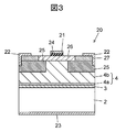
- FIG. 3 is a cross-sectional view of a vertical FET 20 which is a semiconductor element according to the third embodiment.
- the vertical FET 20 includes a semiconductor laminate 1 including a Ga 2 O 3 substrate 2, an AlGaInN buffer layer 3, and a nitride semiconductor layer 4, and ap + region 25 formed by introducing a p-type impurity into the region 4b.
- a Al 0.2 Ga 0.8 N layer 26 formed on the surface of the nitride semiconductor layer 4 (upper surface in FIG.
- the thickness of the region 4b is 6 ⁇ m, and the Si concentration is 1 ⁇ 10 18 / cm 3 .
- the thickness of the p + region 25 is 1 ⁇ m, and the concentration of the p-type impurity is 1 ⁇ 10 18 / cm 3 .
- the Al 0.2 Ga 0.8 N layer 26 does not contain impurities.
- the source electrode 22 and the drain electrode 23 are made of a laminate of a Ti film and an Al film, for example.
- the gate electrode 21 and the gate insulating film 24 are made of, for example, Al and SiO 2 , respectively.
- the vertical FET 20 is an example of a vertical FET having a MIS gate structure that can be formed using the semiconductor stacked body 1.
- FIG. 4 is a cross-sectional view of a vertical FET 30 which is a semiconductor element according to the fourth embodiment.
- the vertical FET 30 is stacked on the semiconductor stacked body 1 including the Ga 2 O 3 substrate 2, the AlGaInN buffer layer 3, and the nitride semiconductor layer 4, and the surface of the nitride semiconductor layer 4 (upper surface in FIG. 4).
- a drain electrode 33 formed on the surface (the lower surface in FIG. 4).
- the thickness of the region 4b is 6 ⁇ m, and the Si concentration is 1 ⁇ 10 16 / cm 3 .
- the thickness of the p + -GaN layer 34 is 1 ⁇ m, and the concentration of the p-type impurity is 1 ⁇ 10 18 / cm 3 .
- the thickness of the n + -GaN layer 35 is 200 nm, and the concentration of the n-type impurity is 1 ⁇ 10 18 / cm 3 .
- the GaN layer 36 does not contain impurities and has a thickness of, for example, 100 nm.
- the Al 0.2 Ga 0.8 N layer 37 does not contain impurities and has a thickness of, for example, 30 nm.
- the source electrode 32 and the drain electrode 33 are made of, for example, a laminate of a Ti film and an Al film.
- the gate electrode 31 is made of, for example, a stacked body of a Ni film and an Au film.
- the vertical FET 30 is an example of a vertical FET having a Schottky gate structure that can be formed using the semiconductor stacked body 1.
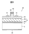
- FIG. 5 is a cross-sectional view of a vertical FET 40 which is a semiconductor device according to the fifth embodiment.
- the vertical FET 40 is formed on the semiconductor stacked body 1 including the Ga 2 O 3 substrate 2, the AlGaInN buffer layer 3, and the nitride semiconductor layer 4, and the surface of the nitride semiconductor layer 4 (upper surface in FIG. 5).
- the thickness of the region 4b is 6 ⁇ m, and the Si concentration is 1 ⁇ 10 18 / cm 3 .
- the thickness of the flat portion of the n ⁇ -GaN layer 44 is 3 ⁇ m, and the concentration of the n-type impurity is 1 ⁇ 10 16 / cm 3 .
- the source electrode 42 is made of, for example, WSi.
- the drain electrode 43 is made of, for example, a laminate of a Ti film and an Al film.
- the gate electrode 41 is made of, for example, PdSi.
- the vertical FET 40 is an example of a vertical FET having a Schottky gate structure that can be formed using the semiconductor stacked body 1.
- HBT heterojunction bipolar transistor
- FIG. 6 is a cross-sectional view of an HBT 50 that is a semiconductor element according to the sixth embodiment.
- the HBT 50 includes a semiconductor stacked body 1 including a Ga 2 O 3 substrate 2, an AlGaInN buffer layer 3, and a nitride semiconductor layer 4, and n stacked on the surface of the nitride semiconductor layer 4 (upper surface in FIG. 6).
- n is stacked on p + -GaN layer 55 + -Al 0.1 Ga 0.9 n layer 56 and n + -GaN layer 57, p + Formed on the base electrode 51 formed on the ⁇ GaN layer 55, the emitter electrode 52 formed on the n + -GaN layer 57, and the surface of Ga 2 O 3 substrate 2 (the lower surface in FIG. 6).
- Collector electrode 53 is
- the thickness of the region 4b is 4 ⁇ m, and the Si concentration is 1 ⁇ 10 18 / cm 3 .
- the thickness of the n ⁇ -GaN layer 54 is 2 ⁇ m and the concentration of the n-type impurity is 1 ⁇ 10 16 / cm 3 .
- the thickness of the p + -GaN layer 55 is 100 nm, and the concentration of the p-type impurity is 1 ⁇ 10 18 / cm 3 .
- the thickness of the n + -Al 0.1 Ga 0.9 N layer 56 is 500 nm, and the concentration of n-type impurities is 1 ⁇ 10 18 / cm 3 .
- the thickness of the n + -GaN layer 57 is 1 ⁇ m, and the concentration of the n-type impurity is 1 ⁇ 10 18 / cm 3 .
- the emitter electrode 52 is made of, for example, a laminate of a Ti film and an Al film.
- the collector electrode 53 is made of, for example, a laminate of a Ti film and an Au film.
- the base electrode 51 is made of, for example, a stacked body of a Ni film and an Au film.
- the HBT 50 is an example of a heterojunction bipolar transistor that can be formed using the semiconductor stacked body 1.
- a Schottky barrier diode (SBD) including the semiconductor multilayer body 1 of the first embodiment will be described.
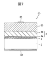
- FIG. 7 is a cross-sectional view of an SBD 60 that is a semiconductor element according to the seventh embodiment.
- the SBD 60 is formed on the semiconductor stacked body 1 including the Ga 2 O 3 substrate 2, the AlGaInN buffer layer 3, and the nitride semiconductor layer 4, and the surface of the nitride semiconductor layer 4 (upper surface in FIG. 7).
- the thickness of the region 4b is 6 ⁇ m, and the Si concentration is 1 ⁇ 10 18 / cm 3 .
- the thickness of the n ⁇ -GaN layer 63 is 7 ⁇ m, and the concentration of the n-type impurity is 1 ⁇ 10 16 / cm 3 .
- the anode electrode 61 is made of, for example, Au.
- the cathode electrode 62 is made of, for example, a laminate of a Ti film and an Au film.
- the SBD 60 is an example of a Schottky barrier diode that can be formed using the semiconductor stacked body 1.
- LED light emitting diode
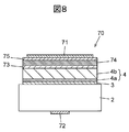
- FIG. 8 is a cross-sectional view of an LED 70, which is a semiconductor element according to the eighth embodiment.
- the LED 70 emits light that is stacked on the semiconductor stacked body 1 including the Ga 2 O 3 substrate 2, the AlGaInN buffer layer 3, and the nitride semiconductor layer 4, and on the surface of the nitride semiconductor layer 4 (upper surface in FIG. 8).
- an n-electrode 72 formed on the substrate.
- the thickness of the region 4b is 5 ⁇ m, and the Si concentration is 1 ⁇ 10 18 / cm 3 .
- Region 4b serves as an n-type cladding layer.
- the light emitting layer 73 includes three pairs of multiple quantum well structures composed of a GaN crystal having a thickness of 8 nm and an InGaN crystal having a thickness of 2 nm.
- the p-type cladding layer 74 is made of a GaN crystal having an Mg concentration of 5.0 ⁇ 10 19 / cm 3 and has a thickness of 150 nm.
- the p-type contact layer 75 is made of a GaN crystal having an Mg concentration of 1.5 ⁇ 10 20 / cm 3 and has a thickness of 10 nm.
- the LED 70 is an example of a light emitting diode that can be formed using the semiconductor laminate 1.
- the Si high concentration region 4a having a Si concentration of 5 ⁇ 10 18 / cm 3 or more in the nitride semiconductor layer 4 is formed.
- the laminated body 1 can be formed. This is considered to be due to the fact that by forming the Si high concentration region 4a having a high Si concentration, electrons tunnel through the potential barrier at the heterointerface, and current flows easily.
- the electrical resistance in the thickness direction of the semiconductor stacked body can be further reduced. Furthermore, by setting the thickness of the AlGaInN buffer layer to 0.5 nm or more and 10 nm or less, the electrical resistance in the thickness direction of the semiconductor stacked body can be further reduced.
- a high-performance vertical semiconductor is formed. An element can be obtained.
- Example 1 a plurality of semiconductor stacked bodies 1 having different impurity concentrations in the Si high concentration region 4a are formed, and the relationship between the impurity concentration in the Si high concentration region 4a and the electrical resistance in the thickness direction of the semiconductor stack 1 is examined. It was.
- the formation process of each semiconductor laminated body 1 is as follows.
- the Ga 2 O 3 substrate 2 was installed in the MOCVD apparatus, and an AlN crystal was grown on the Ga 2 O 3 substrate 2 at a growth temperature of 450 ° C. to form an AlGaInN buffer layer 3 having a thickness of 5 nm.
- a GaN crystal was grown on the AlGaInN buffer layer 3 at a growth temperature of 1050 ° C. while adding Si to form a nitride semiconductor layer 4 having a thickness of 2 ⁇ m.
- the Si addition concentration at the initial stage of growth of the GaN crystal was increased to form a Si high concentration region 4a having a thickness of 10 nm.
- the impurity concentration of the region 4b was 2 ⁇ 10 18 / cm 3 .
- electrodes were formed on the surfaces of the Ga 2 O 3 substrate 2 and the nitride semiconductor layer 4 using photolithography and vapor deposition techniques. Then, a voltage was applied between the electrodes, and the voltage drop when the current density was 200 A / cm 2 was measured.
- FIG. 9 is a graph showing the relationship between the Si concentration in the Si high concentration region 4a and the voltage drop when the current density is 200 A / cm 2 . As shown in FIG. 9, the higher the Si concentration in the Si high concentration region 4a, the smaller the voltage drop, that is, the lower the electrical resistance in the thickness direction of the semiconductor stacked body 1.
- the electrical resistance in the thickness direction of the semiconductor stacked body 1 is low when the Si concentration in the Si high concentration region 4a is 5 ⁇ 10 18 / cm 3 or more. It can also be seen that when the Si concentration in the Si high concentration region 4a is 1 ⁇ 10 19 / cm 3 or more, the value of the voltage drop becomes almost constant.
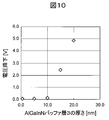
- Example 2 a plurality of different semiconductor stacked bodies 1 are formed within the range of 0.5 to 20 nm in thickness of the AlGaInN buffer layer 3, and the thickness of the AlGaInN buffer layer 3 and the thickness direction of the semiconductor stacked body 1 are The relationship of electrical resistance was investigated.
- the formation process of each semiconductor laminated body 1 is as follows.
- the Ga 2 O 3 substrate 2 was installed in the MOCVD apparatus, and an AlN crystal was grown on the Ga 2 O 3 substrate 2 at a growth temperature of 450 ° C. to form the AlGaInN buffer layer 3.
- a GaN crystal was grown on the AlGaInN buffer layer 3 at a growth temperature of 1050 ° C. while adding Si to form a nitride semiconductor layer 4 having a thickness of 2 ⁇ m.
- the Si addition concentration at the initial stage of growth of the GaN crystal was increased to form a Si high concentration region 4a having a thickness of 10 nm.
- the Si concentrations in the high Si concentration region 4a and the region 4b were 2 ⁇ 10 19 / cm 3 and 2 ⁇ 10 18 / cm 3 , respectively.
- electrodes were formed on the surfaces of the Ga 2 O 3 substrate 2 and the nitride semiconductor layer 4 using photolithography and vapor deposition techniques. Then, a voltage was applied between the electrodes, and the voltage drop when the current density was 200 A / cm 2 was measured.
- FIG. 10 is a graph showing the relationship between the thickness of the AlGaInN buffer layer 3 and the voltage drop when the current density is 200 A / cm 2 . As shown in FIG. 10, the smaller the thickness of the AlGaInN buffer layer 3, the smaller the voltage drop, that is, the lower the electrical resistance in the thickness direction of the semiconductor stacked body 1.
- the thickness of the AlGaInN buffer layer 3 is 10 nm or less, the electrical resistance in the thickness direction of the semiconductor stacked body 1 is low. Further, when the thickness of the AlGaInN buffer layer 3 is thick, even if the Si concentration in the Si high concentration region 4a is sufficiently high (2 ⁇ 10 19 / cm 3 ), the electric resistance in the thickness direction of the semiconductor stacked body 1 It turns out that becomes large.
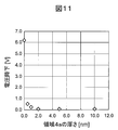
- Example 3 a plurality of different semiconductor stacked bodies 1 are formed within the Si high concentration region 4a having a thickness of 0 to 10 nm, and the thickness of the Si high concentration region 4a and the thickness direction of the semiconductor stacked body 1 are increased.
- the relationship of electrical resistance was investigated.
- the formation process of each semiconductor laminated body 1 is as follows.
- the Ga 2 O 3 substrate 2 was installed in the MOCVD apparatus, and an AlN crystal was grown on the Ga 2 O 3 substrate 2 at a growth temperature of 450 ° C. to form an AlGaInN buffer layer 3 having a thickness of 5 nm.
- a GaN crystal was grown on the AlGaInN buffer layer 3 at a growth temperature of 1050 ° C. while adding Si to form a nitride semiconductor layer 4 having a thickness of 2 ⁇ m.
- the Si addition concentration at the initial stage of growth of the GaN crystal was increased to form the Si high concentration region 4a.
- the Si concentrations in the high Si concentration region 4a and the region 4b were 2 ⁇ 10 19 / cm 3 and 2 ⁇ 10 18 / cm 3 , respectively.
- electrodes were formed on the surfaces of the Ga 2 O 3 substrate 2 and the nitride semiconductor layer 4 using photolithography and vapor deposition techniques. Then, a voltage was applied between the electrodes, and the voltage drop when the current density was 200 A / cm 2 was measured.
- FIG. 11 is a graph showing the relationship between the thickness of the Si high concentration region 4a and the voltage drop when the current density is 200 A / cm 2 . As shown in FIG. 11, the greater the thickness of the high Si concentration region 4a, the smaller the voltage drop, that is, the lower the electrical resistance in the thickness direction of the semiconductor stacked body 1.
- the electrical resistance in the thickness direction of the semiconductor laminate 1 is low when the thickness of the Si high concentration region 4a is 2 nm or more.
- Example 4 the LED70 of the eighth embodiment is formed, and measuring the voltage drop V F forward.
- an n-type ⁇ -Ga 2 O 3 substrate to which Si was added was prepared as a Ga 2 O 3 substrate 2.
- the thickness of the ⁇ -Ga 2 O 3 substrate is 400 ⁇ m, and the main surface is (101).
- an AlGaInN buffer layer 3 was formed on the ⁇ -Ga 2 O 3 substrate by growing 5 nm of AlN crystal at a growth temperature of 450 ° C. using an MOCVD apparatus.
- a GaN crystal having an Si concentration of 2.0 ⁇ 10 19 / cm 3 is grown by 10 nm at a growth temperature of 1050 ° C. to form a Si high concentration region 4a, and subsequently, an Si concentration of 1.0 ⁇ 10 18 / cm 3 is formed.
- a region 4b as an n-type cladding layer was formed by growing a GaN crystal by 5 ⁇ m.
- three pairs of multiple quantum well structures composed of a GaN crystal having a thickness of 8 nm and an InGaN crystal having a thickness of 2 nm were formed at a growth temperature of 750 ° C., and a light emitting layer 73 was formed by further growing the GaN crystal by 10 nm.
- a GaN crystal having an Mg concentration of 5.0 ⁇ 10 19 / cm 3 at a growth temperature of 1000 ° C. was grown to 150 nm to form a p-type cladding layer 74.
- a GaN crystal having an Mg concentration of 1.5 ⁇ 10 20 / cm 3 was grown to 10 nm at a growth temperature of 1000 ° C., and a p-type contact layer 75 was formed.
- TMG trimethylgallium
- TMI trimethylindium
- SiH 3 CH 3 monomethylsilane
- Cp2Mg cyclopentadienylmagnesium
- N source NH 3 ammonia
- the surface of the LED epitaxial wafer produced as described above was etched from the p-type contact layer 75 side to a position deeper than the light emitting layer 73 using an ICP-RIE apparatus to form a mesa shape.
- a SiO 2 film was formed on the side surface of the light emitting layer 73 using a sputtering apparatus.
- electrodes that are ohmic-bonded were formed on the p-type contact layer 75 and the Ga 2 O 3 substrate 2 using a vapor deposition device, and an LED 70 having a light extraction surface on the Ga 2 O 3 substrate 2 side was obtained.
- an LED having an AlGaInN buffer layer 3 with a thickness of 20 nm and no Si high concentration region 4a was formed.
Landscapes
- Chemical & Material Sciences (AREA)
- Engineering & Computer Science (AREA)
- Materials Engineering (AREA)
- Metallurgy (AREA)
- Organic Chemistry (AREA)
- Chemical Kinetics & Catalysis (AREA)
- General Chemical & Material Sciences (AREA)
- Crystallography & Structural Chemistry (AREA)
- Inorganic Chemistry (AREA)
- Mechanical Engineering (AREA)
- Junction Field-Effect Transistors (AREA)
- Chemical Vapour Deposition (AREA)
- Electrodes Of Semiconductors (AREA)
- Bipolar Transistors (AREA)
- Crystals, And After-Treatments Of Crystals (AREA)
Abstract
Description
図1は、第1の実施の形態に係る半導体積層体1の断面図である。半導体積層体1は、Ga2O3基板2と、AlGaInNバッファ層3と、窒化物半導体層4を含む。
第2の実施の形態として、第1の実施の形態の半導体積層体1を含む縦型FET(Field effect transistor)について述べる。
第3の実施の形態として、第1の実施の形態の半導体積層体1を含むMIS(Metal Insulator Semiconductor)ゲート構造の縦型FETについて述べる。
第4の実施の形態として、第1の実施の形態の半導体積層体1を含むショットキーゲート構造の縦型FETについて述べる。
第5の実施の形態として、第1の実施の形態の半導体積層体1を含む他のショットキーゲート構造の縦型FETについて述べる。
第6の実施の形態として、第1の実施の形態の半導体積層体1を含むヘテロ接合バイポーラトランジスタ(HBT)について述べる。
第7の実施の形態として、第1の実施の形態の半導体積層体1を含むショットキーバリアダイオード(SBD)について述べる。
第8の実施の形態として、第1の実施の形態の半導体積層体1を含む発光ダイオード(LED)について述べる。
第1の実施の形態によれば、Si濃度が5×10¹⁸/cm3以上であるSi高濃度領域4aを窒化物半導体層4中に形成することにより、厚さ方向の電気抵抗が低い半導体積層体1を形成することができる。これは、Si濃度の高いSi高濃度領域4aを形成することにより、電子がヘテロ界面の電位障壁をトンネルし、電流が流れやすくなることによると考えられる。
Claims (11)
- Ga2O3基板と、
前記Ga2O3基板上のAlxGayInzN(0≦x≦1、0≦y≦1、0≦z≦1、x+y+z=1)結晶からなるバッファ層と、
前記バッファ層上の、Siを含むAlxGayInzN(0≦x≦1、0≦y≦1、0≦z≦1、x+y+z=1)結晶からなる窒化物半導体層と、
を備え、
前記窒化物半導体層は、前記バッファ層側の一部の領域にSi濃度が5×10¹⁸/cm3以上であるSi高濃度領域を有する、
半導体積層体。 - 前記Si高濃度領域の厚さが2nm以上である、
請求項1に記載の半導体積層体。 - 前記バッファ層の厚さが0.5nm以上10nm以下である、
請求項1又は2に記載の半導体積層体。 - 前記バッファ層の前記AlxGayInzN結晶はAlN結晶である、
請求項1に記載の半導体積層体。 - 前記窒化物半導体層の前記AlxGayInzN結晶はGaN結晶である、
請求項1に記載の半導体積層体。 - Ga2O3基板と、前記Ga2O3基板上のAlxGayInzN(0≦x≦1、0≦y≦1、0≦z≦1、x+y+z=1)結晶からなるバッファ層と、前記バッファ層上の、Siを含むAlxGayInzN(0≦x≦1、0≦y≦1、0≦z≦1、x+y+z=1)結晶からなる窒化物半導体層と、を備え、前記窒化物半導体層は、前記バッファ層側の一部の領域にSi濃度が5×10¹⁸/cm3以上であるSi高濃度領域を有する、半導体積層体を含み、
前記半導体積層体の厚さ方向に通電する、
半導体素子。 - Ga2O3基板上にAlxGayInzN(0≦x≦1、0≦y≦1、0≦z≦1、x+y+z=1)結晶をエピタキシャル成長させてバッファ層を形成する工程と、
前記バッファ層上にSiを添加しつつAlxGayInzN(0≦x≦1、0≦y≦1、0≦z≦1、x+y+z=1)結晶を成長させて窒化物半導体層を形成する工程と、
を含み、
前記AlxGayInzN結晶の成長の初期段階においてSiの添加濃度を大きくすることにより、Si濃度が5×10¹⁸/cm3以上であるSi高濃度領域を前記窒化物半導体層中に形成する、
半導体積層体の製造方法。 - 前記Si高濃度領域は2nm以上の厚さに形成される、
請求項7に記載の半導体積層体の製造方法。 - 前記バッファ層は0.5nm以上10nm以下の厚さに形成される、
請求項7又は8に記載の半導体積層体の製造方法。 - 前記バッファ層の前記AlxGayInzN結晶はAlN結晶である、
請求項7に記載の半導体積層体の製造方法。 - 前記窒化物半導体層の前記AlxGayInzN結晶はGaN結晶である、
請求項7に記載の半導体積層体の製造方法。
Priority Applications (5)
| Application Number | Priority Date | Filing Date | Title |
|---|---|---|---|
| KR1020137029343A KR20140040712A (ko) | 2011-04-08 | 2012-04-03 | 반도체 적층체 및 그 제조 방법, 및 반도체 소자 |
| JP2013508884A JPWO2012137783A1 (ja) | 2011-04-08 | 2012-04-03 | 半導体積層体及びその製造方法、並びに半導体素子 |
| CN201280017340.4A CN103518008A (zh) | 2011-04-08 | 2012-04-03 | 半导体层叠体及其制造方法和半导体元件 |
| DE112012001613.0T DE112012001613T5 (de) | 2011-04-08 | 2012-04-03 | Halbleiterlaminat und Prozess für seine Herstellung und Halbleiterelement |
| US14/110,420 US20140027770A1 (en) | 2011-04-08 | 2012-04-03 | Semiconductor laminate and process for production thereof, and semiconductor element |
Applications Claiming Priority (2)
| Application Number | Priority Date | Filing Date | Title |
|---|---|---|---|
| JP2011-086806 | 2011-04-08 | ||
| JP2011086806 | 2011-04-08 |
Publications (1)
| Publication Number | Publication Date |
|---|---|
| WO2012137783A1 true WO2012137783A1 (ja) | 2012-10-11 |
Family
ID=46969179
Family Applications (1)
| Application Number | Title | Priority Date | Filing Date |
|---|---|---|---|
| PCT/JP2012/059096 Ceased WO2012137783A1 (ja) | 2011-04-08 | 2012-04-03 | 半導体積層体及びその製造方法、並びに半導体素子 |
Country Status (7)
| Country | Link |
|---|---|
| US (1) | US20140027770A1 (ja) |
| JP (1) | JPWO2012137783A1 (ja) |
| KR (1) | KR20140040712A (ja) |
| CN (1) | CN103518008A (ja) |
| DE (1) | DE112012001613T5 (ja) |
| TW (1) | TW201248690A (ja) |
| WO (1) | WO2012137783A1 (ja) |
Cited By (1)
| Publication number | Priority date | Publication date | Assignee | Title |
|---|---|---|---|---|
| JPWO2015146069A1 (ja) * | 2014-03-28 | 2017-04-13 | パナソニックIpマネジメント株式会社 | 発光ダイオード素子 |
Families Citing this family (1)
| Publication number | Priority date | Publication date | Assignee | Title |
|---|---|---|---|---|
| JP7116409B2 (ja) * | 2017-02-27 | 2022-08-10 | 株式会社タムラ製作所 | トレンチmos型ショットキーダイオード |
Citations (3)
| Publication number | Priority date | Publication date | Assignee | Title |
|---|---|---|---|---|
| JP2005340308A (ja) * | 2004-05-24 | 2005-12-08 | Koha Co Ltd | 半導体素子の製造方法 |
| JP2006310765A (ja) * | 2005-03-31 | 2006-11-09 | Toyoda Gosei Co Ltd | 低温成長バッファ層の形成方法、発光素子の製造方法、発光素子、および発光装置 |
| JP2008098245A (ja) * | 2006-10-06 | 2008-04-24 | Showa Denko Kk | Iii族窒化物化合物半導体積層構造体の成膜方法 |
Family Cites Families (8)
| Publication number | Priority date | Publication date | Assignee | Title |
|---|---|---|---|---|
| KR20010029852A (ko) * | 1999-06-30 | 2001-04-16 | 도다 다다히데 | Ⅲ족 질화물계 화합물 반도체 소자 및 그 제조방법 |
| KR100841269B1 (ko) * | 2004-01-26 | 2008-06-25 | 쇼와 덴코 가부시키가이샤 | Ⅲ족 질화물 반도체 다층구조물 |
| EP2071053B1 (en) * | 2006-09-29 | 2019-02-27 | Toyoda Gosei Co., Ltd. | Filming method for iii-group nitride semiconductor laminated structure |
| KR101020958B1 (ko) * | 2008-11-17 | 2011-03-09 | 엘지이노텍 주식회사 | 산화갈륨기판 제조방법, 발광소자 및 발광소자 제조방법 |
| JP5529420B2 (ja) * | 2009-02-09 | 2014-06-25 | 住友電気工業株式会社 | エピタキシャルウエハ、窒化ガリウム系半導体デバイスを作製する方法、窒化ガリウム系半導体デバイス、及び酸化ガリウムウエハ |
| JP5378829B2 (ja) * | 2009-02-19 | 2013-12-25 | 住友電気工業株式会社 | エピタキシャルウエハを形成する方法、及び半導体素子を作製する方法 |
| JP5491116B2 (ja) * | 2009-09-25 | 2014-05-14 | 日本碍子株式会社 | 半導体素子用エピタキシャル基板、半導体素子、および半導体素子用エピタキシャル基板の製造方法 |
| JP5648510B2 (ja) * | 2011-02-04 | 2015-01-07 | 豊田合成株式会社 | Iii族窒化物半導体発光素子の製造方法 |
-
2012
- 2012-04-03 CN CN201280017340.4A patent/CN103518008A/zh active Pending
- 2012-04-03 US US14/110,420 patent/US20140027770A1/en not_active Abandoned
- 2012-04-03 DE DE112012001613.0T patent/DE112012001613T5/de not_active Withdrawn
- 2012-04-03 JP JP2013508884A patent/JPWO2012137783A1/ja active Pending
- 2012-04-03 WO PCT/JP2012/059096 patent/WO2012137783A1/ja not_active Ceased
- 2012-04-03 KR KR1020137029343A patent/KR20140040712A/ko not_active Withdrawn
- 2012-04-06 TW TW101112272A patent/TW201248690A/zh unknown
Patent Citations (3)
| Publication number | Priority date | Publication date | Assignee | Title |
|---|---|---|---|---|
| JP2005340308A (ja) * | 2004-05-24 | 2005-12-08 | Koha Co Ltd | 半導体素子の製造方法 |
| JP2006310765A (ja) * | 2005-03-31 | 2006-11-09 | Toyoda Gosei Co Ltd | 低温成長バッファ層の形成方法、発光素子の製造方法、発光素子、および発光装置 |
| JP2008098245A (ja) * | 2006-10-06 | 2008-04-24 | Showa Denko Kk | Iii族窒化物化合物半導体積層構造体の成膜方法 |
Non-Patent Citations (1)
| Title |
|---|
| KIYOSHI SHIMAMURA ET AL.: "LED no Koseinoka Kokoritsuka Tomei Dodensei Kiban to shite no Sanka Gallium Tankessho no Kaihatsu", GEKKAN DISPLAY, vol. 11, no. 2, 2005, pages 40 - 44 * |
Cited By (1)
| Publication number | Priority date | Publication date | Assignee | Title |
|---|---|---|---|---|
| JPWO2015146069A1 (ja) * | 2014-03-28 | 2017-04-13 | パナソニックIpマネジメント株式会社 | 発光ダイオード素子 |
Also Published As
| Publication number | Publication date |
|---|---|
| KR20140040712A (ko) | 2014-04-03 |
| TW201248690A (en) | 2012-12-01 |
| JPWO2012137783A1 (ja) | 2014-07-28 |
| DE112012001613T5 (de) | 2014-01-16 |
| CN103518008A (zh) | 2014-01-15 |
| US20140027770A1 (en) | 2014-01-30 |
Similar Documents
| Publication | Publication Date | Title |
|---|---|---|
| JP5596222B2 (ja) | 半導体積層体及びその製造方法、並びに半導体素子 | |
| CN103718312B (zh) | 用于氮化物半导体发光元件的制造方法、晶圆以及氮化物半导体发光元件 | |
| US8507891B2 (en) | Group III nitride semiconductor light-emitting device and production method therefor | |
| JP5099008B2 (ja) | SiC基板を用いた化合物半導体装置とその製造方法 | |
| CN103500780B (zh) | 一种氮化镓基led外延结构及其制备方法 | |
| CN105514232B (zh) | 一种发光二极管外延片、发光二极管及外延片的制作方法 | |
| CN103647009A (zh) | 氮化物发光二极管及其制备方法 | |
| JPH1027924A (ja) | 窒素−3族元素化合物半導体発光素子 | |
| CN102790155B (zh) | 氮化物半导体器件和晶片以及制造氮化物半导体层的方法 | |
| CN104993028B (zh) | 一种发光二极管外延片 | |
| KR100784065B1 (ko) | 질화물 반도체 발광소자 및 그 제조방법 | |
| CN100530726C (zh) | Ⅲ-ⅴ族金属氧化物半导体发光场效应晶体管及其制备方法 | |
| JP5460751B2 (ja) | 半導体装置 | |
| JP3705637B2 (ja) | 3族窒化物半導体発光素子及びその製造方法 | |
| CN101276864A (zh) | 发光元件 | |
| JPWO2012137783A1 (ja) | 半導体積層体及びその製造方法、並びに半導体素子 | |
| JP2009076864A (ja) | 窒化物系発光素子 | |
| WO2016002801A1 (ja) | 半導体積層構造体及び半導体素子 | |
| CN109346581B (zh) | 一种发光二极管的外延片及其制备方法 | |
| JP5059205B2 (ja) | ウェーハ及び結晶成長方法 | |
| KR101140679B1 (ko) | 질화갈륨계 화합물 반도체 | |
| JP2013089617A (ja) | 結晶積層構造体及びその製造方法、並びに半導体素子 | |
| JP3700713B2 (ja) | 窒素−3族元素化合物半導体素子 | |
| KR20080000098A (ko) | 질화갈륨계 화합물 반도체 및 그 제조방법 | |
| KR20120041439A (ko) | 질화물계 반도체 소자 및 그의 제조 방법 |
Legal Events
| Date | Code | Title | Description |
|---|---|---|---|
| 121 | Ep: the epo has been informed by wipo that ep was designated in this application |
Ref document number: 12767313 Country of ref document: EP Kind code of ref document: A1 |
|
| ENP | Entry into the national phase |
Ref document number: 2013508884 Country of ref document: JP Kind code of ref document: A |
|
| WWE | Wipo information: entry into national phase |
Ref document number: 14110420 Country of ref document: US |
|
| WWE | Wipo information: entry into national phase |
Ref document number: 112012001613 Country of ref document: DE Ref document number: 1120120016130 Country of ref document: DE |
|
| ENP | Entry into the national phase |
Ref document number: 20137029343 Country of ref document: KR Kind code of ref document: A |
|
| 122 | Ep: pct application non-entry in european phase |
Ref document number: 12767313 Country of ref document: EP Kind code of ref document: A1 |