WO2012137544A1 - 磁気センサ - Google Patents
磁気センサ Download PDFInfo
- Publication number
- WO2012137544A1 WO2012137544A1 PCT/JP2012/053746 JP2012053746W WO2012137544A1 WO 2012137544 A1 WO2012137544 A1 WO 2012137544A1 JP 2012053746 W JP2012053746 W JP 2012053746W WO 2012137544 A1 WO2012137544 A1 WO 2012137544A1
- Authority
- WO
- WIPO (PCT)
- Prior art keywords
- magnetoresistive element
- magnetic sensor
- magnet
- magnets
- magnetoresistive
- Prior art date
- Legal status (The legal status is an assumption and is not a legal conclusion. Google has not performed a legal analysis and makes no representation as to the accuracy of the status listed.)
- Ceased
Links
Images



Classifications
-
- G—PHYSICS
- G01—MEASURING; TESTING
- G01R—MEASURING ELECTRIC VARIABLES; MEASURING MAGNETIC VARIABLES
- G01R33/00—Arrangements or instruments for measuring magnetic variables
- G01R33/0047—Housings or packaging of magnetic sensors ; Holders
-
- G—PHYSICS
- G01—MEASURING; TESTING
- G01R—MEASURING ELECTRIC VARIABLES; MEASURING MAGNETIC VARIABLES
- G01R33/00—Arrangements or instruments for measuring magnetic variables
- G01R33/02—Measuring direction or magnitude of magnetic fields or magnetic flux
- G01R33/06—Measuring direction or magnitude of magnetic fields or magnetic flux using galvano-magnetic devices
- G01R33/09—Magnetoresistive devices
- G01R33/091—Constructional adaptation of the sensor to specific applications
-
- H—ELECTRICITY
- H10—SEMICONDUCTOR DEVICES; ELECTRIC SOLID-STATE DEVICES NOT OTHERWISE PROVIDED FOR
- H10N—ELECTRIC SOLID-STATE DEVICES NOT OTHERWISE PROVIDED FOR
- H10N50/00—Galvanomagnetic devices
- H10N50/10—Magnetoresistive devices
-
- H—ELECTRICITY
- H10—SEMICONDUCTOR DEVICES; ELECTRIC SOLID-STATE DEVICES NOT OTHERWISE PROVIDED FOR
- H10N—ELECTRIC SOLID-STATE DEVICES NOT OTHERWISE PROVIDED FOR
- H10N50/00—Galvanomagnetic devices
- H10N50/80—Constructional details
Definitions
- the present invention relates to a long magnetic sensor that detects a magnetic pattern printed on, for example, banknotes.
- Patent Document 1 is disclosed as a magnetic sensor for discriminating an object to be detected such as a bill or a security printed with a predetermined pattern with magnetic ink or the like.
- the vibration in the fundamental wave mode is a bending vibration in which both ends of the long magnetic sensor are fixed ends.
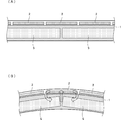
- FIG. 1A shows a state in which no bending stress is applied to the long magnetic sensor.
- a plurality of magnetoresistive elements 2, a plurality of magnets 5 that apply a magnetic field to the magnetic sensing portions of the plurality of magnetoresistive elements 2, and a case 1 that holds the magnetoresistive elements 2 and the magnets 5 are provided. Yes.
- the plurality of magnets 5 and the plurality of magnets 5 are arranged such that the position of the opposing portion between the magnets 5 of the plurality of magnets 5 is the center position of a certain magnetoresistive element 2 of the plurality of magnetoresistive elements 2.
- a resistance element 2 is arranged.
- FIG. 1B is a partial sectional view exaggeratingly showing a state in which bending stress is applied to the long magnetic sensor.
- the case 1 is a resin molded from a resin mold
- the magnetoresistive element 2 and the magnet 5 are softer than the case 1. For this reason, when bending stress is applied to the long magnetic sensor, stress distortion occurs in the magnetoresistive element 2 corresponding to the facing portion (magnet joint position) between the magnet 5 and the magnet 5.
- the magnetoresistive element 2 is made of an n-InSb material, InAs material, GaAs material, Ge material, or Si material having high electron mobility. Such a magnetoresistive element material has a piezoresistive effect. Therefore, when stress strain occurs in the magnetoresistive element 2, a signal due to the piezoresistive effect is superimposed, and this acts as noise (piezonoise).
- the bending stress applied to the magnetoresistive element 2 can be reduced, but not only the distance accuracy between the magnetic sensor and the object to be detected is lowered, but also the amplitude of the bending vibration is increased. End up. Since the detection sensitivity of the magnetic body is affected by the square of the distance between the magnetic sensing portion of each magnetoresistive element of the magnetic sensor and the magnetic body to be detected, a flexible material cannot be used for the case of the magnetic sensor.
- the stress strain applied to the magnetoresistive element 2 is reduced.
- the opposing portion of the magnetoresistive element 2 and the magnetoresistive element 2 naturally has no magnetic sensitive part (disconnected)
- the detection sensitivity of the magnetic material tends to decrease
- the magnet 5 and the magnet 5 Since the opposing part has a tendency that the detection sensitivity of the magnetic material is lowered due to the small magnetic flux density, both sensitivity reduction factors overlap. Therefore, it is difficult to adopt a structure in which the magnet facing portion overlaps the magnetoresistive element facing portion.
- the present invention has been made in view of the above-described problems, and an object thereof is to provide a magnetic sensor that solves the above-described piezo noise problem caused by bending vibration accompanying the increase in length of the magnetic sensor.
- the magnetic sensor of the present invention includes a plurality of magnetoresistive elements, a plurality of magnets, and a case for holding the plurality of magnetoresistive elements and the plurality of magnets, and the case includes the plurality of magnetoresistive elements in series. And a magnet holding part for holding the plurality of magnets in series so as to apply a magnetic field to the magnetoresistive element placed on the magnetoresistive element placing part.
- the plurality of magnets and the plurality of magnetoresistive elements include a magnet facing portion, which is a facing portion between the magnets of the plurality of magnets, and a magnetoresistive element and a magnetoresistive element of the plurality of magnetoresistive elements. Are arranged so as to correspond to positions other than the opposite part of The magnetoresistive element is bonded to the case through an adhesive layer at a part of the surface of the magnetoresistive element facing the case.
- a magnetic sensor in which piezo noise associated therewith is reduced even when bending vibration occurs in the magnetic sensor can be configured.
- FIG. 1A is a cross-sectional view of a conventional general long type magnetic sensor in a state where no bending stress is applied.
- FIG. 1B is a partial cross-sectional view in a state where bending stress is applied to the long magnetic sensor.
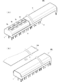
- 2A is an external perspective view in the middle of attaching the cover of the long magnetic sensor 201 according to the first embodiment
- FIG. 2B is an external perspective view in a state in which the cover is attached.
- FIG. 3 is a front view showing a structure in which the magnetic sensor 201 is incorporated into an installation destination device.
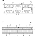
- FIG. 4A is a partial plan view of the magnetic sensor 201 according to the first embodiment with the cover removed.
- FIG. 4B is a partial view of the central longitudinal cross section of the magnetic sensor 201 in the longitudinal direction.
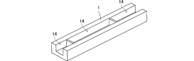
- FIG. 5 is a partial perspective view of the case 1 as viewed from the magnet holding portion 14 side.
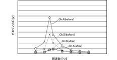
- FIG. 6 shows a comparative example of piezo noise generated between the conventional magnetic sensor and the magnetic sensor 201 according to the first embodiment of the present invention.
- FIG. 7A is a partial plan view of the magnetic sensor 202 of the second embodiment with the cover removed.
- FIG. 7B is a partial view of the central longitudinal cross section of the magnetic sensor 202 in the longitudinal direction.
- FIG. 8A is a partial plan view of the magnetic sensor 203 according to the third embodiment with the cover removed.
- FIG. 8B is a partial view of a central longitudinal section in the longitudinal direction of the magnetic sensor 203.
- FIG. 2A is an external perspective view in the middle of attaching the cover of the long magnetic sensor 201 according to the first embodiment
- FIG. 2B is an external perspective view in a state in which the cover is attached.
- the case 1 made of synthetic resin has magnetoresistive elements 2a, 2b, 2c, 2d.
- a terminal pin 6 that conducts to the plurality of magnetoresistive elements 2a, 2b, 2c, 2d,.
- Claw engaging grooves 3 are provided on both sides of the case 1 along the longitudinal direction.
- the cover 4 made of metal is provided with a cover fixing claw portion that engages with the claw portion engagement groove 3 of the case. As shown, a cover 4 is covered on top of the case 1.
- the object to be detected 100 is conveyed in a direction substantially perpendicular to the longitudinal direction of the long magnetic sensor 201 as indicated by an arrow in the figure.
- FIG. 3 is a front view showing a structure in which the magnetic sensor 201 is incorporated into an installation destination device.
- the magnetic sensor 201 is mounted on the circuit board 110 via the terminal pins 6.
- the circuit board 110 is held by a holder 120, and the holder 120 is fixed to a frame or the like of an installation destination device.
- FIG. 4A is a partial plan view of the magnetic sensor 201 of the first embodiment. However, it is shown with the cover removed.
- FIG. 4B is a partial view of the central longitudinal cross section of the magnetic sensor 201 in the longitudinal direction.
- FIG. 5 is a partial perspective view of the case 1 as viewed from the magnet holding portion 14 side.
- the magnet holding part 14 is a recess formed in the lower part of the case 1, and the magnet 5 is accommodated in the magnet holding part 14.
- the case 1 is resin-molded.
- a plurality of magnetoresistive element mounting portions 13i, 13j, 13k and the like are formed on the upper portion of the case 1.
- Magnets 5 are housed in a plurality of magnet holders 14 formed in the lower part of case 1.
- the magnet 5 is filled with a filler 8 such as an epoxy resin so that the magnet 5 is embedded in the magnet holding portion 14.
- the magnetoresistive elements 2i, 2j, 2k and the like are bonded to the lower surfaces of the magnetoresistive element mounting portions 13i, 13j, 13k and the like via the adhesive layer 7.
- a part of the lower surface of the magnetoresistive element 2j is joined by an adhesive layer 7 to the magnetoresistive element mounting portion 13j corresponding to the position of the facing portion between the magnet 5 and the magnet 5.
- Nearly the entire lower surface of the magnetoresistive elements 2i, 2k is joined by an adhesive layer 7 to the magnetoresistive element mounting portions 13i, 13k, etc. that do not correspond to the positions of the opposing portions of the magnets 5 and 5.
- the magnetoresistive elements 2i, 2j, 2k, etc. are bonded to the magnetoresistive element mounting portion on the opposite side of the magnetosensitive element so that the magnetosensitive part is on the upper surface side.
- the electrode pad of the magnetoresistive element is joined to the inner lead of the lead frame, and the outer lead of the lead frame is thermocompression bonded to the terminal pin 6, but in FIG. Illustration of these leads is omitted.
- the magnetoresistive element that is not at the position of the facing portion between the magnet 5 and the magnet 5 and the height of the magnetosensitive element 2j joined to the magnetoresistive element mounting portion 13j corresponding to the facing portion between the magnet 5 and the magnet 5
- the thickness of the adhesive layer 7 is determined so that the heights of the magnetically sensitive portions such as the magnetoresistive elements 2i and 2k joined to the placement portions 13i and 13k are uniform. For example, when the adhesive is applied to the magnetoresistive element mounting portion with a dispenser or the like, the viscosity of the adhesive and the coating amount are determined, and the magnetoresistive element is mounted on the magnetoresistive element mounting portion.
- the spread area of the adhesive on the lower surface of the magnetoresistive element and the thickness of the adhesive layer are determined. Furthermore, the spread amount of the adhesive layer and the thickness of the adhesive layer may be adjusted by the pressing force of the magnetoresistive element on the magnetoresistive element mounting portion.
- the magnetoresistive element 2j joined to the magnetoresistive element mounting portion 13j of the case 1 corresponding to the position of the facing portion between the magnet 5 and the magnet 5 is a part of the lower surface of the magnetoresistive element mounting portion 13j. 1B, even when bending stress as shown in FIG. 1B is applied to the magnetic sensor 201, the bending moment to the magnetoresistive element 2j is reduced. That is, the flat state is maintained with almost no influence of bending at the position of the facing portion between the magnet 5 and the magnet 5 of the case 1. This suppresses the generation of piezo noise.
- FIG. 6 shows a comparative example of piezo noise generated between the conventional magnetic sensor and the magnetic sensor 201 according to the first embodiment of the present invention.
- Ch.A (before) is piezo noise generated in the channel A of the conventional magnetic sensor
- Ch.B (before) is piezo noise generated in the channel B of the conventional magnetic sensor.
- Ch.A (after) is piezo noise generated in the channel A of the magnetic sensor 201 of the first embodiment
- Ch.B (after) is piezo noise generated in the channel B of the magnetic sensor 201 of the first embodiment. is there.
- the channel A corresponds to the sixth magnetoresistive element corresponding to the position of the opposing portion of the magnet 5 among the 18 channels (18 magnetoresistive elements) in total.
- the channel B corresponds to the eleventh magnetoresistive element corresponding to the position of another facing portion between the magnet 5 and the magnet 5.
- the horizontal axis represents frequency and the vertical axis represents piezo noise voltage. Both are relative value scales. As shown in FIG. 6, since a mountain shape in which piezo noise rises at a predetermined frequency is drawn, it can be seen that bending vibration is generated at the resonance frequency, and large piezo noise is generated at this resonance frequency. Compared to the magnetic sensor having the conventional structure, the piezo noise can be reduced to about 1/6 or less in the magnetic sensor 201 of the first embodiment.
- FIG. 7A is a partial plan view of the magnetic sensor 202 of the second embodiment. However, it is shown with the cover removed.
- FIG. 7B is a partial view of the central longitudinal cross section of the magnetic sensor 202 in the longitudinal direction.
- Case 1 is resin molded.
- a plurality of magnetoresistive element mounting portions 13i, 13j, 13k and the like are formed on the upper portion of the case 1.
- the lower surfaces of these magnetoresistive element mounting portions 13i, 13j, 13k and the like are magnetoresistive element facing surfaces.
- magnet holders 14 that store a plurality of magnets 5 are formed in the lower part of the case 1, and the magnets 5 are stored in these magnet holders 14, respectively.
- the periphery of the magnet 5 is filled with a filler 8 such as an epoxy resin.
- an adhesive layer 9 for the magnetoresistive element 2j is an adhesive layer 9 for the magnetoresistive element 2j.
- an adhesive in which beads defining the thickness of the adhesive layer are mixed is applied to the magnetoresistive element placement portion 13j of the case 1 corresponding to the position of the facing portion between the magnet 5 and the magnet 5. is doing.
- the thickness of the adhesive layer that joins the magnetoresistive element 2j to the magnetoresistive element mounting portion 13j is relatively small, the thickness of the adhesive layer can be controlled only with a normal adhesive. May be difficult.
- the beads for example, silica beads having a particle diameter of 150 ⁇ m to 200 ⁇ m can be used.
- a mixture of the beads with a Si-based adhesive at a certain ratio is used.
- the thickness of the adhesive layer 9 is defined to be approximately equal to the particle size of the beads.
- the thickness of the adhesive layer such as the magnetoresistive elements 2i and 2k on the magnetoresistive element mounting portions 13i and 13k that are not located at the position where the magnet 5 and the magnet 5 face each other is adjusted by, for example, the amount of adhesive applied.
- the thickness of the adhesive layer of the magnetoresistive element 2j on the magnetoresistive element mounting portion 13j corresponding to the position of the facing portion between the magnet 5 and the magnet 5 may be adjusted by the particle size of the beads to be mixed. In this way, the height of the magnetic sensing part of each magnetoresistive element can be made uniform.
- the adhesive applied to the magnetoresistive element mounting portions 13i, 13k, etc. which is not located at the position where the magnet 5 and the magnet 5 face each other, may be an adhesive mixed with beads defining the thickness of the adhesive layer. Good. Further, the particle size and ratio of the beads to be mixed may be different between the adhesive that limits the application range and the adhesive that is applied to the entire surface.
- the piezo noise reduction effect of the magnetic sensor 202 of the second embodiment is substantially the same as that of the magnetic sensor 201 of the first embodiment.
- FIG. 8A is a partial plan view of the magnetic sensor 203 of the third embodiment. However, it is shown with the cover removed.
- FIG. 8B is a partial view of a central longitudinal section in the longitudinal direction of the magnetic sensor 203.
- the difference from the first and second embodiments is a configuration for increasing the thickness of the adhesive layer provided on the magnetoresistive element mounting portion 13j of the case 1 corresponding to the position of the facing portion between the magnet 5 and the magnet 5. is there. That is, the engraved portion 12 is formed on almost the entire surface of the magnetoresistive element mounting portion 13j. Therefore, in the state where the thickness of the adhesive layer provided on the magnetoresistive element mounting portion 13j is thicker than the thickness of the adhesive layer provided on the other magnetoresistive element mounting portions 13i, 13k, etc. The height of can be made constant.
- the thickness of the adhesive layer 7 provided on the magnetoresistive element mounting portion 13j corresponding to the position of the facing portion between the magnet 5 and the magnet 5 is relatively thick, the bonding strength of the magnetoresistive element 2j with a limited application area Can be maintained sufficiently.
- the elasticity of the adhesive layer 7 acts effectively, stress strain on the magnetoresistive element 2j when bending stress is applied to the magnetic sensor is further reduced.
- the adhesive used for joining the magnetoresistive element 2j is the bead mixed adhesive shown in the second embodiment, and the thickness of the adhesive layer 7 provided on the magnetoresistive element mounting portion 13j is defined by the particle size of the beads. You may do it.
- the piezo noise reduction effect of the magnetic sensor 203 of the third embodiment is substantially the same as that of the magnetic sensor 201 of the first embodiment.
Landscapes
- Physics & Mathematics (AREA)
- Condensed Matter Physics & Semiconductors (AREA)
- General Physics & Mathematics (AREA)
- Measuring Magnetic Variables (AREA)
Abstract
ケース(1)の上部に複数の磁気抵抗素子載置部(13i,13j,13k)等が形成されている。また、ケース(1)の下部には複数の磁石(5)を収納する磁石保持部(14)が形成されていて、これらの磁石保持部(14)に磁石(5)がそれぞれ収納されている。磁石(5)と磁石(5)との対向部の位置に対応する磁気抵抗素子載置部(13j)には磁気抵抗素子(2j)の下面の一部が接着剤層(7)で接合されている。磁石(5)と磁石(5)との対向部の位置に対応していない磁気抵抗素子載置部(13i,13k)等には磁気抵抗素子(2i,2k)の下面のほぼ全面が接着剤層(7)で接合されている。これにより、磁気センサの長尺化に伴って共振振動による屈曲振動の振幅が大きくなってもピエゾノイズが生じにくい磁気センサを構成する。
Description
この発明は例えば紙幣などに印刷されている磁気パターンを検出する長尺型の磁気センサに関するものである。
磁性インクなどで所定パターンが印刷された紙幣や証券などの被検知物の鑑別を行う磁気センサとして特許文献1が開示されている。
長尺型磁気センサの設置環境によっては、外部から磁気センサに機械的な振動が加わる。例えばATM中に備えられているモータやそのモータによって駆動される機構の振動が磁気センサに伝搬される。磁気センサが長尺になる程、その自己共振周波数は低くなるので、磁気センサは前記モータや機構による振動に共振しやすくなる傾向にある。そして、長尺化に伴ってその振動振幅も大きくなる傾向にある。
長尺型磁気センサは紙幣などの搬送経路を阻害しない状態で装置に保持することが必要であることから、磁気センサの両端部が装置内の保持部に保持される場合が多い。そのとき、基本波モードでの振動は長尺型磁気センサの両端を固定端とする屈曲振動となる。
ここで、特許文献1に記載されている長尺型磁気センサの基本的な構成を部分断面図で図1に示す。図1(A)は長尺型磁気センサに対して曲げ応力が掛かっていない状態である。複数の磁気抵抗素子2と、これら複数の磁気抵抗素子2の感磁部に対して磁界を印加する複数の磁石5と、これらの磁気抵抗素子2および磁石5を保持するケース1とを備えている。複数の磁石5のうちの磁石5と磁石5との対向部の位置が複数の磁気抵抗素子2のうちの或る磁気抵抗素子2の中央位置になるように、複数の磁石5および複数の磁気抵抗素子2が配置されている。
図1(B)は前記長尺型磁気センサに曲げ応力が加わった状態を誇張して表した部分断面図である。ケース1は樹脂モールドによる成型樹脂であるので磁気抵抗素子2および磁石5はケース1より軟質である。そのため、長尺型磁気センサに曲げ応力が加わると、磁石5と磁石5との対向部(磁石の継ぎ目位置)に対応する磁気抵抗素子2に応力歪みが生じる。磁気抵抗素子2は電子移動度の高いn-InSb材やInAs材、GaAs材、Ge材、Si材が用いられる。このような磁気抵抗素子材料はピエゾ抵抗効果を有する。そのため、磁気抵抗素子2に応力歪みが生じるとピエゾ抵抗効果による信号が重畳されることになり、これがノイズ(ピエゾノイズ)として作用する。
前記ケース1に比較的柔らかい樹脂材料を用いれば、磁気抵抗素子2に掛かる曲げ応力が低減できるが、磁気センサと被検知対象物との距離精度が低下するばかりか屈曲振動の振幅も増大してしまう。磁性体の検知感度は磁気センサの各磁気抵抗素子の感磁部と検知対象の磁性体との距離の二乗で影響を受けるので、磁気センサのケースに柔軟性材料を用いることはできない。
また、磁石5と磁石5との対向部の位置を磁気抵抗素子2と磁気抵抗素子2との対向部の位置に一致させれば、磁気抵抗素子2に加わる応力歪みは小さくなる。しかし、磁気抵抗素子2と磁気抵抗素子2との対向部は当然に感磁部が無い(途切れている)ので、磁性体の検知感度が低下する傾向にあり、且つ磁石5と磁石5との対向部は磁束密度が小さいことで磁性体の検知感度が低下する傾向にあるので、双方の感度低下要因が重なる。したがって、磁石対向部が磁気抵抗素子対向部に重なるような構造は採りにくい。
本発明は上述の問題に鑑みてなされたものであり、その目的は磁気センサの長尺化に伴う屈曲振動により生じる前記ピエゾノイズの問題を解消した磁気センサを提供することにある。
本発明の磁気センサは、複数の磁気抵抗素子と、複数の磁石と、前記複数の磁気抵抗素子および前記複数の磁石を保持するケースと、を備え、前記ケースは前記複数の磁気抵抗素子を直列に載置する磁気抵抗素子載置部および前記磁気抵抗素子載置部に載置される磁気抵抗素子に対して磁界を印加するように前記複数の磁石を直列状態で保持する磁石保持部を有する磁気センサにおいて、
前記複数の磁石および前記複数の磁気抵抗素子は、前記複数の磁石のうちの磁石と磁石との対向部である磁石対向部が前記複数の磁気抵抗素子のうちの磁気抵抗素子と磁気抵抗素子との対向部以外の位置に対応するように配置され、
前記ケースに対する前記磁気抵抗素子の対向面の一部で接着剤層を介して前記磁気抵抗素子を前記ケースに接合させたことを特徴とする。
前記複数の磁石および前記複数の磁気抵抗素子は、前記複数の磁石のうちの磁石と磁石との対向部である磁石対向部が前記複数の磁気抵抗素子のうちの磁気抵抗素子と磁気抵抗素子との対向部以外の位置に対応するように配置され、
前記ケースに対する前記磁気抵抗素子の対向面の一部で接着剤層を介して前記磁気抵抗素子を前記ケースに接合させたことを特徴とする。
本発明によれば、磁気センサに屈曲振動が生じてもそれに伴うピエゾノイズが低減された磁気センサを構成できる。
《第1の実施形態》
図2(A)は第1の実施形態に係る長尺型磁気センサ201のカバーの取り付け途中の外観斜視図、図2(B)はそのカバーが取り付けられた状態での外観斜視図である。合成樹脂製のケース1にはその上部に磁気抵抗素子2a,2b,2c,2d・・・が取り付けられている。ケース1の下部には、複数の磁気抵抗素子2a,2b,2c,2d・・・に導通する端子ピン6が突出している。ケース1の両側部には長手方向に沿って爪部係合溝3が設けられている。
図2(A)は第1の実施形態に係る長尺型磁気センサ201のカバーの取り付け途中の外観斜視図、図2(B)はそのカバーが取り付けられた状態での外観斜視図である。合成樹脂製のケース1にはその上部に磁気抵抗素子2a,2b,2c,2d・・・が取り付けられている。ケース1の下部には、複数の磁気抵抗素子2a,2b,2c,2d・・・に導通する端子ピン6が突出している。ケース1の両側部には長手方向に沿って爪部係合溝3が設けられている。
金属製のカバー4には、ケースの爪部係合溝3に係合するカバー固定爪部が設けられていて、両者の係合状態で長手方向にスライドさせることによって、図2(B)に示すようにケース1の上部にカバー4が覆われる。被検知物100は図中矢印で示すように長尺型磁気センサ201の長手方向に略直交する向きに搬送される。
図3は組み込み先機器への前記磁気センサ201の組み込み構造を示す正面図である。磁気センサ201は前記端子ピン6を介して回路基板110に実装されている。回路基板110は保持具120で保持され、この保持具120は組み込み先機器のフレームなどに固定される。
図4(A)は第1の実施形態の磁気センサ201の部分平面図である。但し、カバーを取り除いた状態で示している。図4(B)は磁気センサ201の長手方向の中央縦断面の部分図である。
図5は、ケース1を磁石保持部14側から見た部分斜視図である。磁石保持部14はケース1の下部に形成された凹部であり、この磁石保持部14内に磁石5が収納される。
図4(A)、図4(B)に示すように、ケース1は樹脂モールド成型されたものである。このケース1の上部に複数の磁気抵抗素子載置部13i,13j,13k等が形成されている。ケース1の下部に形成された複数磁石保持部14にそれぞれ磁石5が収納されている。これらの磁石保持部14内に磁石5を埋設するように、磁石5の周囲は例えばエポキシ系樹脂などの充填材8で充填されている。
磁気抵抗素子載置部13i,13j,13k等の下面には磁気抵抗素子2i,2j,2k等が接着剤層7を介して接合されている。磁石5と磁石5との対向部の位置に対応する磁気抵抗素子載置部13jには磁気抵抗素子2jの下面の一部が接着剤層7で接合されている。磁石5と磁石5との対向部の位置に対応していない磁気抵抗素子載置部13i,13k等には磁気抵抗素子2i,2kの下面のほぼ全面が接着剤層7で接合されている。
磁気抵抗素子2i,2j,2k等は、感磁部が上面側になるように、感磁部とは反対側の面が磁気抵抗素子載置部に接着されている。なお、図2(A)に表れているように、磁気抵抗素子の電極パッドはリードフレームのインナーリードに接合され、このリードフレームのアウターリードが端子ピン6に熱圧着されるが、図4ではこれらのリードの図示を省略している。
磁石5と磁石5との対向部に対応する磁気抵抗素子載置部13jに接合される磁気抵抗素子2jの感磁部の高さと、磁石5と磁石5との対向部の位置でない磁気抵抗素子載置部13i,13k等に接合される磁気抵抗素子2i,2k等の感磁部の高さは一定に揃うように、接着剤層7の厚みが定められている。例えば、磁気抵抗素子載置部に対してディスペンサー等で接着剤を塗布する際、接着剤の粘度とその塗布量を定めておき、磁気抵抗素子載置部に磁気抵抗素子を載置したときに、磁気抵抗素子の下面への接着剤の拡がり面積と接着剤層の厚みを定める。また、さらには磁気抵抗素子載置部への磁気抵抗素子の押圧力によって接着剤層の拡がり量と接着剤層の厚みを調整してもよい。
このように、磁石5と磁石5との対向部の位置に対応するケース1の磁気抵抗素子載置部13jに接合される磁気抵抗素子2jはその下面の一部で磁気抵抗素子載置部13jに接合されていることにより、図1(B)に示したような曲げ応力が磁気センサ201に加わっても、磁気抵抗素子2jへの曲げモーメントが低減される。すなわち、ケース1の磁石5と磁石5との対向部の位置でのベンディングの影響を殆ど受けずに平坦な状態を保つ。このことによりピエゾノイズの発生は抑えられる。
ここで、この実施形態によるピエゾノイズの低減効果の例を示す。
図6は従来構造の磁気センサと本発明の第1の実施形態の磁気センサ201について発生するピエゾノイズの比較例である。図6において、Ch.A(before)は従来構造の磁気センサのチャンネルAに発生するピエゾノイズ、Ch.B(before)は従来構造の磁気センサのチャンネルBに発生するピエゾノイズである。また、Ch.A(after)は第1の実施形態の磁気センサ201のチャンネルAに発生するピエゾノイズ、Ch.B(after)は第1の実施形態の磁気センサ201のチャンネルBに発生するピエゾノイズである。ここで、チャンネルAは、全部で18チャンネル(18個の磁気抵抗素子)のうち、磁石5と磁石5との対向部の位置に対応する6番目の磁気抵抗素子に相当する。また、チャンネルBは、磁石5と磁石5との別の対向部の位置に対応する11番目の磁気抵抗素子に相当する。
図6は従来構造の磁気センサと本発明の第1の実施形態の磁気センサ201について発生するピエゾノイズの比較例である。図6において、Ch.A(before)は従来構造の磁気センサのチャンネルAに発生するピエゾノイズ、Ch.B(before)は従来構造の磁気センサのチャンネルBに発生するピエゾノイズである。また、Ch.A(after)は第1の実施形態の磁気センサ201のチャンネルAに発生するピエゾノイズ、Ch.B(after)は第1の実施形態の磁気センサ201のチャンネルBに発生するピエゾノイズである。ここで、チャンネルAは、全部で18チャンネル(18個の磁気抵抗素子)のうち、磁石5と磁石5との対向部の位置に対応する6番目の磁気抵抗素子に相当する。また、チャンネルBは、磁石5と磁石5との別の対向部の位置に対応する11番目の磁気抵抗素子に相当する。
図6において横軸は周波数、縦軸はピエゾノイズの電圧である。いずれも相対値目盛りである。図6に表れているように、所定の周波数でピエゾノイズが上昇する山形を描いていることから共振周波数で屈曲振動し、この共振周波数で大きなピエゾノイズが発生することがわかる。従来構造の磁気センサに比較して第1の実施形態の磁気センサ201ではピエゾノイズは約1/6以下に低減できている。
《第2の実施形態》
図7(A)は第2の実施形態の磁気センサ202の部分平面図である。但し、カバーを取り除いた状態で示している。図7(B)は磁気センサ202の長手方向の中央縦断面の部分図である。
図7(A)は第2の実施形態の磁気センサ202の部分平面図である。但し、カバーを取り除いた状態で示している。図7(B)は磁気センサ202の長手方向の中央縦断面の部分図である。
ケース1は樹脂モールド成型されたものである。このケース1の上部に複数の磁気抵抗素子載置部13i,13j,13k等が形成されている。これらの磁気抵抗素子載置部13i,13j,13k等の下面が磁気抵抗素子対向面である。また、ケース1の下部には複数の磁石5を収納する磁石保持部14が形成されていて、これらの磁石保持部14にそれぞれ磁石5が収納されている。磁石保持部14内で、磁石5の周囲は例えばエポキシ系樹脂等の充填材8で充填されている。
第1の実施形態と異なるのは磁気抵抗素子2jに対する接着剤層9である。この第2の実施形態では、磁石5と磁石5との対向部の位置に対応するケース1の磁気抵抗素子載置部13jに、接着剤層の厚みを規定するビーズを混合した接着剤を塗布している。
磁石5と磁石5との対向部の位置でない磁気抵抗素子載置部13i,13k等に接合される磁気抵抗素子2i,2k等はそれらの下面の全面が接着剤で濡れるように接着剤を塗布すればよいので、その制御は比較的容易である。一方、磁気抵抗素子載置部13jに磁気抵抗素子2jを接合する接着剤層の厚みは接着剤の塗布量が相対的に少ないため、通常の接着剤だけでは接着剤層の厚みを制御することが困難な場合がある。前記ビーズとしては例えば粒径150μm~200μmのシリカビーズを用いることができる。このビーズを例えばSi系の接着剤に対して一定割合で混合したものを用いる。このことにより、接着剤層9の厚みはビーズの粒径にほぼ等しい寸法に規定される。
したがって、磁石5と磁石5との対向部の位置でない磁気抵抗素子載置部13i,13k等への磁気抵抗素子2i,2k等の接着剤層の厚みは、例えば接着剤の塗布量で調整し、磁石5と磁石5との対向部の位置に対応する磁気抵抗素子載置部13jへの磁気抵抗素子2jの接着剤層の厚みは、混合するビーズの粒径で調整すればよい。
このようにして各磁気抵抗素子の感磁部の高さを一定に揃えることができる。
このようにして各磁気抵抗素子の感磁部の高さを一定に揃えることができる。
勿論、磁石5と磁石5との対向部の位置でない磁気抵抗素子載置部13i,13k等へ塗布する接着剤についても、接着剤層の厚みを規定するビーズを混合した接着剤を用いてもよい。また、塗布範囲を制限する接着剤と全面に塗布する接着剤とで、混合する
ビーズの粒径や割合を異ならせてもよい。
ビーズの粒径や割合を異ならせてもよい。
第2の実施形態の磁気センサ202のピエゾノイズの低減効果は第1の実施形態の磁気センサ201と実質的に同じであることを確かめている。
《第3の実施形態》
図8(A)は第3の実施形態の磁気センサ203の部分平面図である。但し、カバーを取り除いた状態で示している。図8(B)は磁気センサ203の長手方向の中央縦断面の部分図である。第1・第2の実施形態と異なるのは磁石5と磁石5との対向部の位置に対応するケース1の磁気抵抗素子載置部13jに設ける接着剤層の厚みを厚くするための構成である。すなわち、磁気抵抗素子載置部13jのほぼ全面に彫り込み部12を形成している。そのため、この磁気抵抗素子載置部13jに設ける接着剤層の厚みを他の磁気抵抗素子載置部13i,13k等に設ける接着剤層の厚みより厚くした状態で各磁気抵抗素子の感磁部の高さを一定に揃えることができる。
図8(A)は第3の実施形態の磁気センサ203の部分平面図である。但し、カバーを取り除いた状態で示している。図8(B)は磁気センサ203の長手方向の中央縦断面の部分図である。第1・第2の実施形態と異なるのは磁石5と磁石5との対向部の位置に対応するケース1の磁気抵抗素子載置部13jに設ける接着剤層の厚みを厚くするための構成である。すなわち、磁気抵抗素子載置部13jのほぼ全面に彫り込み部12を形成している。そのため、この磁気抵抗素子載置部13jに設ける接着剤層の厚みを他の磁気抵抗素子載置部13i,13k等に設ける接着剤層の厚みより厚くした状態で各磁気抵抗素子の感磁部の高さを一定に揃えることができる。
磁石5と磁石5との対向部の位置に対応する磁気抵抗素子載置部13jに設ける接着剤層7の厚みが相対的に厚いことにより、限られた塗布面積で磁気抵抗素子2jの接合強度を必要充分に保つことができる。また、接着剤層7の弾性が有効に作用するので、磁気センサに曲げ応力が加わった際の磁気抵抗素子2jに対する応力歪みがより低減される。
なお、磁気抵抗素子2jの接合に用いる接着剤を第2の実施形態で示したビーズ混合接着剤とし、磁気抵抗素子載置部13jに設ける接着剤層7の厚みをビーズの粒径で規定するようにしてもよい。
この第3の実施形態の磁気センサ203のピエゾノイズの低減効果は第1の実施形態の磁気センサ201と実質的に同じであることを確かめている。
《他の実施形態》
以上に示した各実施形態では、ケース1の磁石5と磁石5との対向部の位置に対応する磁気抵抗素子載置部13jに対して接着剤の塗布量や塗布範囲を制限した例を示したが、磁気センサの曲げによって応力が殆ど掛からない磁気抵抗素子載置部13i,13k等についても接着剤の塗布量や塗布範囲を制限してもよい。例えばすべての磁気抵抗素子載置部に磁気抵抗素子をその中央部でのみ接着剤層を介して接合してもよい。
以上に示した各実施形態では、ケース1の磁石5と磁石5との対向部の位置に対応する磁気抵抗素子載置部13jに対して接着剤の塗布量や塗布範囲を制限した例を示したが、磁気センサの曲げによって応力が殆ど掛からない磁気抵抗素子載置部13i,13k等についても接着剤の塗布量や塗布範囲を制限してもよい。例えばすべての磁気抵抗素子載置部に磁気抵抗素子をその中央部でのみ接着剤層を介して接合してもよい。
1…ケース
2…磁気抵抗素子
2a,2b,2c,2d…磁気抵抗素子
2i,2j,2k…磁気抵抗素子
3…爪部係合溝
4…カバー
5…磁石
6…端子ピン
7,9…接着剤層
8…充填材
13i,13j,13k…磁気抵抗素子載置部
14…磁石保持部
100…被検知物
110…回路基板
120…保持具
201~203…磁気センサ
2…磁気抵抗素子
2a,2b,2c,2d…磁気抵抗素子
2i,2j,2k…磁気抵抗素子
3…爪部係合溝
4…カバー
5…磁石
6…端子ピン
7,9…接着剤層
8…充填材
13i,13j,13k…磁気抵抗素子載置部
14…磁石保持部
100…被検知物
110…回路基板
120…保持具
201~203…磁気センサ
Claims (4)
- 複数の磁気抵抗素子と、複数の磁石と、前記複数の磁気抵抗素子および前記複数の磁石を保持するケースと、を備え、前記ケースは前記複数の磁気抵抗素子を直列に載置する磁気抵抗素子載置部および前記磁気抵抗素子載置部に載置される磁気抵抗素子に対して磁界を印加するように前記複数の磁石を直列状態で保持する磁石保持部を有する磁気センサにおいて、
前記複数の磁石および前記複数の磁気抵抗素子は、前記複数の磁石のうちの磁石と磁石との対向部である磁石対向部が前記複数の磁気抵抗素子のうちの磁気抵抗素子と磁気抵抗素子との対向部以外の位置に対応するように配置され、
前記ケースに対する前記磁気抵抗素子の対向面の一部で接着剤層を介して前記磁気抵抗素子を前記ケースに接合させたことを特徴とする磁気センサ。 - 前記接着剤層は、この接着剤層の厚みを規定するビーズが混在した接着剤で構成された、請求項1に記載の磁気センサ。
- 前記磁石対向部の位置に対応する前記磁気抵抗素子載置部に対して前記磁気抵抗素子を接合する接着剤層の厚みは他の磁気抵抗素子の接合剤層の厚みより厚い、請求項1または2に記載の磁気センサ。
- 前記磁石対向部の位置に対応する前記磁気抵抗素子載置部の面を他の磁気抵抗素子載置部の面より低くした、請求項3に記載の磁気センサ。
Applications Claiming Priority (2)
| Application Number | Priority Date | Filing Date | Title |
|---|---|---|---|
| JP2011081933 | 2011-04-01 | ||
| JP2011-081933 | 2011-04-01 |
Publications (1)
| Publication Number | Publication Date |
|---|---|
| WO2012137544A1 true WO2012137544A1 (ja) | 2012-10-11 |
Family
ID=46968948
Family Applications (1)
| Application Number | Title | Priority Date | Filing Date |
|---|---|---|---|
| PCT/JP2012/053746 Ceased WO2012137544A1 (ja) | 2011-04-01 | 2012-02-17 | 磁気センサ |
Country Status (1)
| Country | Link |
|---|---|
| WO (1) | WO2012137544A1 (ja) |
Cited By (2)
| Publication number | Priority date | Publication date | Assignee | Title |
|---|---|---|---|---|
| JP2016125861A (ja) * | 2014-12-26 | 2016-07-11 | セイコーNpc株式会社 | 磁気ラインセンサ |
| JP2016125860A (ja) * | 2014-12-26 | 2016-07-11 | セイコーNpc株式会社 | 磁気ラインセンサにおける磁石の位置決め方法及び位置決め装置 |
Citations (2)
| Publication number | Priority date | Publication date | Assignee | Title |
|---|---|---|---|---|
| WO2005083457A1 (ja) * | 2004-02-27 | 2005-09-09 | Murata Manufacturing Co., Ltd. | 長尺型磁気センサ |
| JP2006220506A (ja) * | 2005-02-09 | 2006-08-24 | Denso Corp | 回転角検出装置 |
-
2012
- 2012-02-17 WO PCT/JP2012/053746 patent/WO2012137544A1/ja not_active Ceased
Patent Citations (2)
| Publication number | Priority date | Publication date | Assignee | Title |
|---|---|---|---|---|
| WO2005083457A1 (ja) * | 2004-02-27 | 2005-09-09 | Murata Manufacturing Co., Ltd. | 長尺型磁気センサ |
| JP2006220506A (ja) * | 2005-02-09 | 2006-08-24 | Denso Corp | 回転角検出装置 |
Cited By (2)
| Publication number | Priority date | Publication date | Assignee | Title |
|---|---|---|---|---|
| JP2016125861A (ja) * | 2014-12-26 | 2016-07-11 | セイコーNpc株式会社 | 磁気ラインセンサ |
| JP2016125860A (ja) * | 2014-12-26 | 2016-07-11 | セイコーNpc株式会社 | 磁気ラインセンサにおける磁石の位置決め方法及び位置決め装置 |
Similar Documents
| Publication | Publication Date | Title |
|---|---|---|
| JP4492432B2 (ja) | 物理量センサ装置の製造方法 | |
| CN110567573B (zh) | 高灵敏度输出压电振动传感器被测激振力信号的方法 | |
| JP5579190B2 (ja) | 圧電式加速度センサ | |
| CN101738492B (zh) | 传感器装置和运行传感器装置的方法 | |
| US20170176186A1 (en) | Angular velocity sensor having support substrates | |
| JP2015224903A (ja) | 圧力センサ、マイクロフォン、超音波センサ、血圧センサ及びタッチパネル | |
| CN101730877A (zh) | 触摸传感装置 | |
| JP6316516B2 (ja) | 磁気センサ装置 | |
| JP7115242B2 (ja) | 磁気センサ | |
| WO2012137543A1 (ja) | 磁気センサ | |
| JP5429013B2 (ja) | 物理量センサ及びマイクロフォン | |
| WO2012137544A1 (ja) | 磁気センサ | |
| JP2002350260A (ja) | 半導体圧力センサ | |
| WO2012098901A1 (ja) | 加速度センサ | |
| JP5107461B2 (ja) | 磁気センサパッケージ | |
| JP2007263951A (ja) | 磁気センサ | |
| CN104094612B (zh) | 音响发生器、音响发生装置以及电子设备 | |
| JP7331468B2 (ja) | 慣性センサーユニットの取り付け方法、および慣性センサーユニット | |
| JP2007064649A (ja) | 加速度センサ | |
| CN100588970C (zh) | 加速度传感器及使用该加速度传感器的磁盘装置 | |
| JP4862840B2 (ja) | 回転検出装置の調整方法 | |
| JP7601977B2 (ja) | 振動センサ | |
| JP2006194712A (ja) | 慣性センサ | |
| JP4393322B2 (ja) | 半導体圧力センサ | |
| JP4393323B2 (ja) | 半導体圧力センサ |
Legal Events
| Date | Code | Title | Description |
|---|---|---|---|
| 121 | Ep: the epo has been informed by wipo that ep was designated in this application |
Ref document number: 12768034 Country of ref document: EP Kind code of ref document: A1 |
|
| NENP | Non-entry into the national phase |
Ref country code: DE |
|
| 122 | Ep: pct application non-entry in european phase |
Ref document number: 12768034 Country of ref document: EP Kind code of ref document: A1 |
|
| NENP | Non-entry into the national phase |
Ref country code: JP |