WO2012137484A1 - 撮像装置 - Google Patents
撮像装置 Download PDFInfo
- Publication number
- WO2012137484A1 WO2012137484A1 PCT/JP2012/002319 JP2012002319W WO2012137484A1 WO 2012137484 A1 WO2012137484 A1 WO 2012137484A1 JP 2012002319 W JP2012002319 W JP 2012002319W WO 2012137484 A1 WO2012137484 A1 WO 2012137484A1
- Authority
- WO
- WIPO (PCT)
- Prior art keywords
- bias voltage
- correlation
- detection film
- temperature
- imaging device
- Prior art date
- Legal status (The legal status is an assumption and is not a legal conclusion. Google has not performed a legal analysis and makes no representation as to the accuracy of the status listed.)
- Ceased
Links
Images




Classifications
-
- H—ELECTRICITY
- H04—ELECTRIC COMMUNICATION TECHNIQUE
- H04N—PICTORIAL COMMUNICATION, e.g. TELEVISION
- H04N23/00—Cameras or camera modules comprising electronic image sensors; Control thereof
- H04N23/30—Cameras or camera modules comprising electronic image sensors; Control thereof for generating image signals from X-rays
Definitions
- the present invention relates to an imaging device used in the medical field, the industrial field, and the nuclear field.
- the imaging apparatus includes an X-ray sensitive X-ray conversion layer, and the X-ray conversion layer converts into carriers (charge information) by the incidence of X-rays.
- the “direct conversion type” that directly converts X-rays into charge information and the X-rays converted into light by a phosphor (scintillator) such as CsI are formed of a light-sensitive material. It is roughly classified into “indirect conversion type” in which the light is converted into charge information by the conversion layer.
- amorphous amorphous selenium (a-Se) film has been conventionally used as the X-ray conversion layer, but in recent years, CdTe (cadmium telluride) or CdZnTe (cadmium zinc telluride) is used. ) Is used.
- the imaging apparatus includes a circuit that accumulates and reads out carriers converted by the X-ray conversion layer.
- this circuit is composed of a plurality of gate lines G and data lines D arranged two-dimensionally, and also turns on a capacitor Ca for accumulating carriers and a carrier accumulated in the capacitor Ca.
- Thin film transistors (TFTs) Tr that are read out by switching between / OFF are arranged in a two-dimensional manner.
- the gate line G controls ON / OFF switching of each thin film transistor Tr and is electrically connected to the gate of each thin film transistor Tr.
- the data line D is electrically connected to the reading side of the thin film transistor Tr.
- Each detection element is constituted by each capacitor Ca, each thin film transistor Tr, and the like.
- the gate line G By selecting the gate line G, the detection element electrically connected to the selected gate line G is driven to generate a carrier. Is read out. Therefore, the gate line G serves as a drive line for driving the detection element.
- X-rays to be detected are made incident with a bias voltage applied to a voltage application electrode (not shown in FIG. 6) (see, for example, Patent Document 1).
- the present invention has been made in view of such circumstances, and an object thereof is to provide an imaging apparatus capable of obtaining desired detection film characteristics.
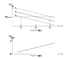
- FIG. 4A is a graph schematically showing the correlation between the dynamic range for each temperature and the bias voltage
- FIG. 4B schematically shows the correlation between the spatial resolution and the bias voltage. It is a graph. As is clear from each graph of FIG.
- the imaging apparatus is an imaging apparatus that includes a detector configured with a two-dimensional matrix array of detection elements for detecting light or radiation, and obtains an image based on data detected by the detector.
- a correlation storage means for storing a correlation between a detection film characteristic in the detector and a bias voltage applied to the detector; and the detection film characteristic and the bias voltage stored in the correlation storage means
- bias voltage setting control means for setting and controlling the bias voltage on the basis of the correlation and the detection film characteristic to be set.
- the correlation storage means for storing the correlation between the detection film characteristic and the bias voltage
- the detection film characteristic and the bias voltage stored in the correlation storage means Bias voltage setting control means for setting and controlling the bias voltage on the basis of the correlation between the two and the detection film characteristics to be set.
- the bias is determined according to the detection film characteristics to be set using the correlation between the detection film characteristics and the bias voltage stored in the correlation storage means. If the voltage setting control means controls the setting of the bias voltage, the detection film characteristic to be set becomes a desired detection film characteristic when the bias voltage is applied with the setting-controlled bias voltage. As a result, desired detection film characteristics can be obtained.
- the correlation storage means further includes the correlation between the detection film characteristic and the bias voltage.
- the bias voltage setting control means preferably stores and controls the bias voltage based on the temperature at which the detector is used and the correlation with the temperature is stored. For example, the optimum bias voltage can be set and controlled for each of several environmental temperatures (for example, the standard set temperature of -5 ° C to + 5 ° C) that the detector is expected to use, so that the setting can be changed according to the usage environment. To do.
- the correlation storage means further stores the correlation with the temperature in addition to the correlation between the dynamic range or the leakage current and the bias voltage.
- an example of a detection film in the detector is a semiconductor layer formed of CdTe (cadmium telluride) or CdZnTe (cadmium zinc telluride).
- the correlation storage means for storing the correlation between the detection film characteristic and the bias voltage, the correlation between the detection film characteristic and the bias voltage stored in the correlation storage means, and the setting are made.
- a desired detection film characteristic can be obtained by providing bias voltage setting control means for setting and controlling the bias voltage based on the power detection film characteristic.
- FIG. 1 is a schematic block diagram of an X-ray imaging apparatus according to an embodiment. 1 is a schematic cross-sectional view around an X-ray conversion layer of an X-ray imaging apparatus.
- (A) is a table of the correlation between the dynamic range for each temperature and the bias voltage
- (b) is a table of the correlation between the spatial resolution and the bias voltage.
- (A) is a graph schematically showing the correlation between the dynamic range for each temperature and the bias voltage
- (b) is a graph schematically showing the correlation between the spatial resolution and the bias voltage. It is the graph which showed roughly the correlation of the leakage current for every temperature and bias voltage which concern on a modification.
- It is a schematic block diagram of the conventional X-ray imaging apparatus.
- FIG. 1 is a schematic block diagram of the X-ray imaging apparatus according to the embodiment
- FIG. 2 is a schematic cross-sectional view around the X-ray conversion layer of the X-ray imaging apparatus.
- X-rays will be described as an example of incident radiation
- an X-ray imaging apparatus will be described as an example of an imaging apparatus.
- the X-ray imaging apparatus performs imaging by irradiating a subject with X-rays. Specifically, an X-ray image transmitted through the subject is projected onto an X-ray conversion layer (CdTe or CdZnTe in this embodiment), and carriers (charge information) proportional to the density of the image are generated in the layer. Is converted into a carrier.
- X-ray conversion layer CdTe or CdZnTe in this embodiment
- the X-ray imaging apparatus accumulates and reads out carriers converted by a gate drive circuit 1 that selects a gate line G, which will be described later, and an X-ray conversion layer 23 (see FIG. 2).
- a detection element circuit 2 that detects X-rays
- a charge-voltage conversion amplifier 3 that amplifies the carrier read out by the detection element circuit 2 into a voltage
- the charge-voltage conversion amplifier 3 An A / D converter 4 for converting a voltage analog value into a digital value, and an image processing unit 5 for obtaining an image by performing signal processing on the voltage value converted into a digital value by the A / D converter 4;
- the controller 6 that controls the circuits 1 and 2, the charge / voltage conversion amplifier 3, the A / D converter 4, the image processing unit 5, the memory unit 7 and the monitor 9 described later, and the processed image are stored.
- Memory section 7 An input unit 8 for setting, and a monitor 9 for displaying the processed images.
- information such as a carrier and an image is image information related to the image.
- the X-ray conversion layer 23 corresponds to the detection film in the present invention, and the detection element circuit 2 corresponds to the detector in the present invention.
- the gate drive circuit 1 is electrically connected to a plurality of gate lines G.
- a thin film transistor (TFT) Tr described later is turned on to release reading of carriers accumulated in a capacitor Ca described later, and the voltage applied to each gate line G Is stopped (the voltage is set to ⁇ 10 V), and the thin film transistor Tr is turned off to block carrier reading.
- the thin film transistor Tr is turned off by applying a voltage to each gate line G to cut off carrier reading and stopping the voltage to each gate line G to turn on and release carrier reading. It may be configured.
- the detection element circuit 2 includes a plurality of gate lines G and data lines D arranged in a two-dimensional manner, and switches the capacitor Ca that accumulates carriers and the carriers accumulated in the capacitor Ca to ON / OFF.
- the thin film transistors Tr to be read out are arranged in a two-dimensional manner.
- the gate line G controls ON / OFF switching of each thin film transistor Tr and is electrically connected to the gate of each thin film transistor Tr.
- the data line D is electrically connected to the reading side of the thin film transistor Tr.
- the gate line G includes 10 gate lines G1 to G10
- the data line D includes 10 data lines D1 to D10.
- the gate lines G1 to G10 are respectively connected to the gates of ten thin film transistors Tr arranged in parallel in the X direction in FIG. 1, and the data lines D1 to D10 are arranged in parallel in the Y direction in FIG.
- Each of the ten thin film transistors Tr is connected to the reading side.
- a capacitor Ca is electrically connected to the side opposite to the reading side of the thin film transistor Tr, and the number of the thin film transistor Tr and the capacitor Ca corresponds one to one.
- the detection elements DU are patterned on the insulating substrate 21 in a two-dimensional matrix arrangement.
- the gate lines G1 to G10 and the data lines D1 to D10 described above are wired on the surface of the insulating substrate 21 by using a thin film forming technique by various vacuum deposition methods or a pattern technique by a photolithography method, and the thin film transistor Tr and capacitor Ca, the carrier collection electrode 22, the X-ray conversion layer 23, and the voltage application electrode 24 are laminated in order.
- the detection element DU corresponds to the detection element in the present invention.
- the X-ray conversion layer 23 is formed of an X-ray sensitive semiconductor thick film (detection film).
- the semiconductor layer is formed of CdTe (cadmium telluride) or CdZnTe (cadmium zinc telluride). It is formed with.
- the X-ray conversion layer 23 converts X-ray information into carriers that are charge information by the incidence of X-rays.
- the X-ray conversion layer 23 is not limited to CdTe or CdZnTe as long as it is an X-ray sensitive material that generates carriers by the incidence of X radiation.
- a radiation-sensitive substance that generates carriers by the incidence of radiation may be used instead of the X-ray conversion layer 23.
- a photosensitive material that generates carriers by the incidence of light may be used instead of the X-ray conversion layer 23.
- the carrier collection electrode 22 is electrically connected to the capacitor Ca, collects the carrier converted by the X-ray conversion layer 23, and accumulates it in the capacitor Ca.
- a large number (10 ⁇ 10 in this embodiment) of the carrier collection electrodes 22 are formed in a vertical / horizontal two-dimensional matrix arrangement.
- the carrier collecting electrode 22, the capacitor Ca, and the thin film transistor Tr are separately formed as each detecting element DU.
- the voltage application electrode 24 is formed over the entire surface as a common electrode of all the detection elements DU.
- the insulating substrate 21, the X-ray conversion layer 23, and the voltage application electrode 24 on which the detection elements DU and the like are patterned in a two-dimensional matrix arrangement are sequentially stacked.
- the detection element circuit 2 including these X-ray conversion layers 23 is also called a flat panel X-ray detector (FPD: Flat Panel Detector).
- a temperature sensor 10 for measuring the temperature of the X-ray conversion layer 23 is provided.
- the measurement result by the temperature sensor 10 is sent to the controller 6.
- the temperature sensor 10 the temperature at which the detection element circuit 2 is used, and hence the environmental temperature, is measured.
- the temperature sensor 10 is provided on the voltage application electrode 24 at the end portion outside the effective detection area (not shown). Specifically, the temperature sensor 10 may be embedded in the voltage application electrode 24 as shown in FIG. 2A, or the temperature sensor 10 is laminated on the voltage application electrode 24 as shown in FIG. May be. Note that the temperature sensor may be embedded in the X-ray conversion layer 23 or the temperature sensor 10 may be stacked on the X-ray conversion layer 23.
- the image processing unit 5 performs various signal processing on the voltage value converted into a digital value by the A / D converter 4 to obtain an image.
- the controller 6 comprehensively controls the circuits 1 and 2, the charge / voltage conversion amplifier 3, the A / D converter 4, the image processing unit 5, a memory unit 7 and a monitor 9 described later, and in this embodiment, a detection film characteristic described later. And a function of setting and controlling the bias voltage (function of bias voltage setting control) based on the correlation between the bias voltage and the detection film characteristic to be set.
- the image processing unit 5 and the controller 6 are configured by a combination of a central processing unit (CPU) and a programmable logic device (FPGA).
- the controller 6 corresponds to the bias voltage setting control means in this invention.
- the memory unit 7 writes and stores image information and the like, and the image information and the like are read from the memory unit 7 in response to a read command from the controller 6.
- the memory unit 7 includes a storage medium represented by ROM (Read-only Memory), RAM (Random-Access Memory), and the like. Note that a RAM is used for writing image information.
- ROM Read-only Memory
- RAM Random-Access Memory
- a ROM is used for writing image information.
- a program relating to a control sequence for setting and controlling the bias voltage is stored in the memory unit 7 based on the above-described correlation and the detection film characteristics to be set, and the control sequence is stored in the controller 6 by reading the program. Let it run.
- the memory unit 7 includes a correlation memory unit 7a that stores the above-described correlation in advance.
- the correlation memory unit 7a corresponds to the correlation storage means in this invention.
- the input unit 8 includes a pointing device represented by a mouse, keyboard, joystick, trackball, touch panel, or the like, or input means such as a button, switch, or lever.
- a pointing device represented by a mouse, keyboard, joystick, trackball, touch panel, or the like
- input means such as a button, switch, or lever.
- a control sequence of the X-ray imaging apparatus of the present embodiment will be described. While applying a bias voltage V A of the voltage application electrode 24 to a high voltage (e.g., several 10V ⁇ number about 100 V), thereby applying X-rays to be detected. Note that the bias voltage V A is not a fixed value but is selected and controlled by the controller 6 as will be apparent from the description below.
- a target gate line G is selected by a scanning signal (that is, a gate driving signal) for reading a signal (here, carrier) of the gate driving circuit 1.
- a scanning signal that is, a gate driving signal
- the scanning signal for reading signals from the gate driving circuit 1 is a signal for applying a voltage (for example, about 15 V) to the gate line G.
- the target gate line G is selected from the gate drive circuit 1, and each thin film transistor Tr connected to the selected gate line G is selected and designated. A voltage is applied to the gate of the thin film transistor Tr selected and designated by this selection designation to turn on. Carriers accumulated from the capacitors Ca connected to the selected and designated thin film transistors Tr are read out to the data line D via the thin film transistors Tr that have been designated and designated to be turned on. That is, the detection element DU related to the selected gate line G is selected and designated, and carriers accumulated in the capacitor Ca of the selected and designated detection element DU are read out to the data line D.
- the charge-voltage conversion amplifier 3 connected to the data line D is reset, and the thin film transistor Tr is turned on (that is, the gate is turned on), whereby the carrier is read out to the data line D. Then, it is amplified in a state converted into voltage by the charge-voltage conversion amplifier 3.
- the address (address) designation of each detection element DU is performed based on the scanning signal for signal reading from the gate drive circuit 1 and the selection of the charge-voltage conversion amplifier 3 connected to the data line D.
- the gate line G1 is selected from the gate drive circuit 1, the detection element DU related to the selected gate line G1 is selected and specified, and the carriers accumulated in the capacitor Ca of the selected and specified detection element DU are all stored.
- Data line D is read out simultaneously, and after sample hold, data lines D1 to D10 are converted into digital values by A / D converter 4 in this order.
- the gate line G2 is selected from the gate drive circuit 1, and the detection element DU related to the selected gate line G2 is selected and specified in the same procedure, and is stored in the capacitor Ca of the selected detection element DU. All the data lines D are read out simultaneously, and after sample-holding, the data lines D1 to D10 are converted into digital values by the A / D converter 4 in order. Similarly, the remaining gate lines G are sequentially selected to read out a two-dimensional carrier.
- Each read carrier is amplified in a state of being converted into a voltage by the charge / voltage conversion amplifier 3 and converted from an analog value to a digital value by the A / D converter 4.
- the image processing unit 5 Based on the voltage value converted into the digital value, the image processing unit 5 performs various signal processing to obtain a two-dimensional image.
- the obtained two-dimensional image and image information represented by a carrier are written and stored in the memory unit 7 via the controller 6, and are read from the memory unit 7 via the controller 6 as necessary. Further, the image information is displayed on the monitor 9 via the controller 6.
- FIG. 3A is a table showing the correlation between the dynamic range for each temperature and the bias voltage
- FIG. 3B is a table showing the correlation between the spatial resolution and the bias voltage
- FIG. 4 is a graph schematically showing the correlation between the dynamic range and the bias voltage for each temperature
- FIG. 4B is a graph schematically showing the correlation between the spatial resolution and the bias voltage.
- the detection film characteristics are not particularly limited as long as the characteristics depend on the X-ray conversion layer 23 (see FIG. 2) corresponding to the detection film, and in this embodiment, the dynamic range (DR: dynamic range) and spatial resolution ( MTF: (Modulation (Transfer (Function)))
- the optimum value of the bias voltage to be applied is associated with the dynamic range and spatial resolution of an image acquired by each apparatus.
- the correlation between the dynamic range and the bias voltage is written and stored in the correlation memory unit 7a, and the correlation between the spatial resolution and the bias voltage is written and stored in the correlation memory unit 7a.
- the correlation memory unit 7a it may be stored in the table format shown in FIG. 3, for example, or may be stored as an approximate expression program shown in FIG.
- the correlation is performed as shown in FIG. Specifically, as shown in FIG. 3 (a), associates the bias voltage V 1 and the dynamic range DR 11 at ambient temperatures T 1, and a bias voltage V 2 and the dynamic range DR 12 at ambient temperatures T 1 correspondence, following similar manner by associating at ambient temperatures T 1 and the bias voltage and the dynamic range, respectively, stores a correlation between the dynamic range and the bias voltage for each environmental temperature T 1 of a table format. Similarly, as shown in FIG.
- the correlation between the spatial resolution and the bias voltage is written and stored in the correlation memory unit 7a as shown in FIG. 3B.
- the bias voltage V 1 and the spatial resolution MTF 11 are associated
- the bias voltage V 2 and the spatial resolution MTF 12 are associated, and so on. Is correlated with each spatial resolution, and the correlation between the spatial resolution and the bias voltage is stored in a table format.
- the bias voltage is set and controlled with reference to the detection film characteristics (dynamic range and spatial resolution) other than the table format shown in FIG. 3, the bias voltage is set and controlled with reference to the closest detection film characteristics. To do.
- the bias voltage may be interpolated from the correlation stored in the table format. For example, when the correlation is expressed by a linear relationship as shown in FIG. 4, the bias voltage is set and controlled from the dynamic range (DR 11 + DR 12 ) / 2 of the intermediate value between the dynamic ranges DR 11 and DR 12.
- an intermediate value (V 1 + V 2 ) / 2 between the bias voltages V 1 and V 2 corresponding to the dynamic ranges DR 11 and DR 12 is obtained as a bias voltage, and the obtained bias voltage (V It is only necessary to perform setting control to a value of 1 + V 2 ) / 2.
- the table format shown in FIG. 3 is a set of discrete values, it may be approximated by a function as shown in FIG. 4, and the program of the approximate expression may be written and stored in the correlation memory unit 7a. By storing the approximate expression program in this way, it is possible to set and control the bias voltage with a continuous value.
- the approximate expression may be obtained by using the least square method. Further, the approximation formula is not limited to the relationship of the linear formula as shown in FIG. May be.
- the dynamic range DR decreases.
- the spatial resolution MTF increases, and an image with good spatial resolution is captured and acquired. can do.
- the environmental temperature is T 1 ⁇ T 2 ⁇ T 3
- the environmental temperature is relatively high as compared with the case where the environmental temperature is relatively low (eg, T 1 ).
- T 3 the leak current decreases at the same bias voltage V, and the dynamic range DR increases.
- the optimum bias voltage for example, the standard set temperature of ⁇ 5 ° C. to + 5 ° C.
- T 1 , T 2 , T 3 for example, the standard set temperature of ⁇ 5 ° C. to + 5 ° C.
- V 1 , V 2 , V 3 the bias voltage
- V 1, V 2, V 3 and the bias voltages V 1 in FIG. 4, V 2, V 3 in FIG. 3 is a separate value.
- the controller 6 (see FIG. 4) according to the detection film characteristic to be set (for example, DR bottom in FIG. 4A) at the time of use after shipment. 1) set and control the bias voltage.
- DR bottom is set as the value of the dynamic range DR to be kept to the minimum
- the value of V 1 is selected as the bias voltage and controlled at the environmental temperature T 1 as shown in FIG.
- control values for V 2 when the environmental temperature T 2 is selected as a bias voltage.
- the value of V 3 is selected as the bias voltage and set and controlled.
- the temperature of the X-ray conversion layer 23 may be measured by the temperature sensor 10 (see FIG. 2).
- the value of the environmental temperature may be input by the input unit 8 (see FIG. 1).
- the controller 6 controls the setting of the bias voltage, the dynamic range DR bottom to be set becomes the desired dynamic range when the bias voltage is applied with the setting controlled.
- the method for setting and controlling the bias voltage in accordance with the spatial resolution to be set is the same as the method for setting and controlling the bias voltage in accordance with the dynamic range, and thus the description thereof is omitted.
- the X-ray imaging apparatus includes the correlation memory unit 7a that stores the correlation between the detection film characteristics (dynamic range and spatial resolution in the present embodiment) and the bias voltage, and includes a correlation memory.
- Bias voltage for setting and controlling the bias voltage based on the correlation between the detection film characteristic (dynamic range and spatial resolution) stored in the unit 7a and the bias voltage and the detection film characteristic (dynamic range and spatial resolution) to be set
- the controller 6 has a setting control function. By providing the correlation memory unit 7a and the bias voltage setting control function in this way, the correlation between the detection film characteristics (dynamic range and spatial resolution) stored in the correlation memory unit 7a and the bias voltage is used.
- the bias voltage setting control function controls the bias voltage according to the detection film characteristics to be set (dynamic range and spatial resolution)
- the detection film characteristics to be set are the desired detection film properties (dynamic range and spatial resolution).
- desired detection film characteristics dynamic range and spatial resolution
- the correlation memory unit In addition to the correlation between the detection film characteristic (dynamic range) and the bias voltage, 7a further stores the correlation with the temperature as shown in FIG. 3A or FIG. Based on the temperature at which the detection element circuit 2) is used, the bias voltage setting control function sets and controls the bias voltage. For example, the optimum bias voltage is set and controlled for each of a plurality of environmental temperatures (for example, the standard set temperature of ⁇ 5 ° C. to + 5 ° C.) where the detector (detection element circuit 2) is expected to be used. The setting can be changed accordingly.
- a plurality of environmental temperatures for example, the standard set temperature of ⁇ 5 ° C. to + 5 ° C.
- the correlation memory unit 7a is further connected to the temperature as shown in FIG. 3A or FIG. 4A in addition to the correlation between the dynamic range and the bias voltage. The correlation is memorized.
- a semiconductor layer formed of CdTe (cadmium telluride) or CdZnTe (cadmium zinc telluride) as a detection film (X-ray conversion layer 23 in this embodiment) in the detector (detection element circuit 2). Is taken as an example.
- the present invention is not limited to the above embodiment, and can be modified as follows.
- the X-ray imaging apparatus as shown in FIG. 1 has been described as an example.
- the present invention is also applicable to an X-ray fluoroscopic imaging apparatus disposed on a C-type arm, for example. May be.
- the present invention may also be applied to an X-ray CT apparatus.
- the present invention provides a “direct conversion type” detection element circuit in which radiation represented by incident X-rays is directly converted into charge information by an X-ray conversion layer (conversion layer).
- conversion layer X-ray conversion layer
- an indirect conversion type detection element circuit that converts incident radiation into light by a conversion layer such as a scintillator and converts the light into charge information by a conversion layer formed of a photosensitive material The present invention may be applied.
- the detection element circuit for detecting X-rays has been described as an example.
- the present invention uses a radioisotope (RI) as in an ECT (Emission-Computed-Tomography) apparatus.
- the detection element circuit is not particularly limited as long as it is a detection element circuit for detecting radiation, as exemplified by a detection element circuit for detecting ⁇ -rays emitted from an administered subject.
- the present invention is not particularly limited as long as it is an apparatus that performs imaging by incidence of radiation, as exemplified by the above-described ECT apparatus.
- the voltage application electrode 24 has a structure as shown in FIG. 2, but the present invention is also applied to a structure having a graphite substrate that also serves as a support substrate and a voltage application electrode, for example. be able to.
- the dynamic range and the spatial resolution have been described as examples of the detection film characteristics.
- the characteristics are not particularly limited as long as the characteristics depend on the detection film as described above.
- the detection film characteristics may be leakage current, sensitivity (related to charge), response (in time), and the like.
- the detection film characteristic is a leakage current, as in the dynamic range, in addition to the correlation between the leakage current and the bias voltage, as shown in FIG. Good.
- the leakage current L increases as the bias voltage V increases.
- the leakage current L increases at the same bias voltage V when the environmental temperature is relatively high (for example, T 3 ).
- the correlation between the detection film characteristic and the bias voltage is written and stored in the correlation memory unit 7a at the time of shipment.
- the correlation memory unit 7a may be configured to be rewritable to the correlation at the time of use after shipment. Therefore, even when the correlation changes over time, it is possible to cope with it.
Landscapes
- Engineering & Computer Science (AREA)
- Multimedia (AREA)
- Signal Processing (AREA)
- Solid State Image Pick-Up Elements (AREA)
- Transforming Light Signals Into Electric Signals (AREA)
- Measurement Of Radiation (AREA)
Abstract
Description
すなわち、この発明に係る撮像装置は、光または放射線を検出する検出素子を2次元マトリックス状配列で構成された検出器を備え、その検出器で検出されたデータに基づいて画像を得る撮像装置であって、前記検出器における検出膜特性と、前記検出器に印加するバイアス電圧との相関関係を記憶する相関関係記憶手段と、その相関関係記憶手段に記憶された前記検出膜特性と前記バイアス電圧との前記相関関係、および設定すべき前記検出膜特性に基づいて、前記バイアス電圧を設定制御するバイアス電圧設定制御手段とを備えることを特徴とするものである。
図1は、実施例に係るX線撮影装置の概略ブロック図であり、図2は、X線撮影装置のX線変換層周辺の概略断面図である。本実施例では、入射する放射線としてX線を例に採って説明するとともに、撮像装置としてX線撮影装置を例に採って説明する。
6 … コントローラ
7a … 相関関係メモリ部
23 … X線変換層
DU … 検出素子
T … 温度
V … バイアス電圧
DR … ダイナミックレンジ
MTF … 空間解像度
L … リーク電流
Claims (16)
- 光または放射線を検出する検出素子を2次元マトリックス状配列で構成された検出器を備え、その検出器で検出されたデータに基づいて画像を得る撮像装置であって、
前記検出器における検出膜特性と、前記検出器に印加するバイアス電圧との相関関係を記憶する相関関係記憶手段と、
その相関関係記憶手段に記憶された前記検出膜特性と前記バイアス電圧との前記相関関係、および設定すべき前記検出膜特性に基づいて、前記バイアス電圧を設定制御するバイアス電圧設定制御手段と
を備えることを特徴とする撮像装置。 - 請求項1に記載の撮像装置において、
前記相関関係記憶手段は、前記検出膜特性と前記バイアス電圧との相関関係の他に、さらに温度との相関関係を記憶し、
前記検出器を使用する温度に基づいて、前記バイアス電圧設定制御手段は前記バイアス電圧を設定制御することを特徴とする撮像装置。 - 請求項2に記載の撮像装置において、
前記検出膜特性は、ダイナミックレンジであって、
前記相関関係記憶手段は、前記ダイナミックレンジと前記バイアス電圧との相関関係の他に、さらに温度との相関関係を記憶することを特徴とする撮像装置。 - 請求項2に記載の撮像装置において、
前記検出膜特性は、リーク電流であって、
前記相関関係記憶手段は、前記リーク電流と前記バイアス電圧との相関関係の他に、さらに温度との相関関係を記憶することを特徴とする撮像装置。 - 請求項2から請求項4のいずれかに記載の撮像装置において、
前記光または前記放射線をキャリアに変換する変換層を検出膜として備えるとともに、
前記変換層の温度を測定する温度センサを備え、
前記温度センサを備えることで前記検出器を使用する温度を測定することを特徴とする撮像装置。 - 請求項5に記載の撮像装置において、
前記バイアス電圧を印加する電圧印加電極を備え、
前記電圧印加電極に前記温度センサを設けることを特徴とする撮像装置。 - 請求項5に記載の撮像装置において、
前記変換層に前記温度センサを設けることを特徴とする撮像装置。 - 請求項2から請求項7のいずれかに記載の撮像装置において、
前記温度毎に各前記バイアス電圧と各前記検出膜特性とを対応付けることにより前記相関関係記憶手段はテーブル形式で記憶することを特徴とする撮像装置。 - 請求項8に記載の撮像装置において、
前記テーブル形式以外の検出膜特性を参照してバイアス電圧を設定制御する場合には、テーブル形式で記憶された相関関係からバイアス電圧を補間することを特徴とする撮像装置。 - 請求項2から請求項7のいずれかに記載の撮像装置において、
前記温度毎に前記バイアスと前記検出膜特性とを関数で近似して、近似式のプログラムを前記相関関係記憶手段は記憶することを特徴とする撮像装置。 - 請求項1に記載の撮像装置において、
各前記バイアス電圧と各前記検出膜特性とを対応付けることにより前記相関関係記憶手段はテーブル形式で記憶することを特徴とする撮像装置。 - 請求項11に記載の撮像装置において、
前記テーブル形式以外の検出膜特性を参照してバイアス電圧を設定制御する場合には、テーブル形式で記憶された相関関係からバイアス電圧を補間することを特徴とする撮像装置。 - 請求項1に記載の撮像装置において、
前記バイアスと前記検出膜特性とを関数で近似して、近似式のプログラムを前記相関関係記憶手段は記憶することを特徴とする撮像装置。 - 請求項1から請求項13のいずれかに記載の撮像装置において、
前記検出膜特性は、空間解像度であって、
前記相関関係記憶手段は、前記空間解像度と前記バイアス電圧との相関関係を記憶することを特徴とする撮像装置。 - 請求項1から請求項14のいずれかに記載の撮像装置において、
前記光または前記放射線をキャリアに変換する変換層を検出膜として備えるとともに、
前記バイアス電圧を印加する電圧印加電極と、
パターン形成された絶縁基板と
を備え、
前記絶縁基板,前記変換層および前記電圧印加電極を順に積層形成することを特徴とする撮像装置。 - 請求項1から請求項15のいずれかに記載の撮像装置において、
前記検出器における検出膜は、CdTe(テルル化カドミウム)またはCdZnTe(テルル化カドミウム亜鉛)で形成された半導体層であることを特徴とする撮像装置。
Priority Applications (1)
| Application Number | Priority Date | Filing Date | Title |
|---|---|---|---|
| JP2013533436A JP5725188B2 (ja) | 2011-04-04 | 2012-04-03 | 撮像装置 |
Applications Claiming Priority (2)
| Application Number | Priority Date | Filing Date | Title |
|---|---|---|---|
| JP2011082864 | 2011-04-04 | ||
| JP2011-082864 | 2011-04-04 |
Publications (1)
| Publication Number | Publication Date |
|---|---|
| WO2012137484A1 true WO2012137484A1 (ja) | 2012-10-11 |
Family
ID=46968893
Family Applications (1)
| Application Number | Title | Priority Date | Filing Date |
|---|---|---|---|
| PCT/JP2012/002319 Ceased WO2012137484A1 (ja) | 2011-04-04 | 2012-04-03 | 撮像装置 |
Country Status (2)
| Country | Link |
|---|---|
| JP (1) | JP5725188B2 (ja) |
| WO (1) | WO2012137484A1 (ja) |
Citations (7)
| Publication number | Priority date | Publication date | Assignee | Title |
|---|---|---|---|---|
| JPS61229357A (ja) * | 1985-04-03 | 1986-10-13 | Matsushita Electric Ind Co Ltd | 光電変換装置 |
| JPH1194532A (ja) * | 1997-09-22 | 1999-04-09 | Toshiba Corp | X線固体平面検出器及びx線診断装置 |
| JPH11331703A (ja) * | 1998-03-20 | 1999-11-30 | Toshiba Corp | 撮像装置 |
| JP2000356680A (ja) * | 1999-06-11 | 2000-12-26 | Hitachi Medical Corp | 半導体放射線検出装置 |
| JP2001257940A (ja) * | 2000-03-13 | 2001-09-21 | Olympus Optical Co Ltd | 撮像装置 |
| JP2007330440A (ja) * | 2006-06-14 | 2007-12-27 | Shimadzu Corp | X線透視撮影装置 |
| JP2010087563A (ja) * | 2008-09-29 | 2010-04-15 | Fujifilm Corp | 残像補正方法および装置 |
-
2012
- 2012-04-03 WO PCT/JP2012/002319 patent/WO2012137484A1/ja not_active Ceased
- 2012-04-03 JP JP2013533436A patent/JP5725188B2/ja active Active
Patent Citations (7)
| Publication number | Priority date | Publication date | Assignee | Title |
|---|---|---|---|---|
| JPS61229357A (ja) * | 1985-04-03 | 1986-10-13 | Matsushita Electric Ind Co Ltd | 光電変換装置 |
| JPH1194532A (ja) * | 1997-09-22 | 1999-04-09 | Toshiba Corp | X線固体平面検出器及びx線診断装置 |
| JPH11331703A (ja) * | 1998-03-20 | 1999-11-30 | Toshiba Corp | 撮像装置 |
| JP2000356680A (ja) * | 1999-06-11 | 2000-12-26 | Hitachi Medical Corp | 半導体放射線検出装置 |
| JP2001257940A (ja) * | 2000-03-13 | 2001-09-21 | Olympus Optical Co Ltd | 撮像装置 |
| JP2007330440A (ja) * | 2006-06-14 | 2007-12-27 | Shimadzu Corp | X線透視撮影装置 |
| JP2010087563A (ja) * | 2008-09-29 | 2010-04-15 | Fujifilm Corp | 残像補正方法および装置 |
Also Published As
| Publication number | Publication date |
|---|---|
| JPWO2012137484A1 (ja) | 2015-02-23 |
| JP5725188B2 (ja) | 2015-05-27 |
Similar Documents
| Publication | Publication Date | Title |
|---|---|---|
| US9625585B1 (en) | Radiation imaging apparatus and method of controlling radiation imaging apparatus | |
| US8642970B2 (en) | Radiographic image detecting apparatus and radiographic image capturing system | |
| JP6853729B2 (ja) | 放射線撮像装置、放射線撮像システム、放射線撮像装置の制御方法及びプログラム | |
| JP5625833B2 (ja) | 放射線検出器および放射線撮影装置 | |
| US20080226031A1 (en) | Radiation imaging apparatus, and method and program for controlling radiation imaging apparatus | |
| US9910172B2 (en) | Temperature compensation for thin film transistors in digital X-ray detectors | |
| CN102577356A (zh) | 放射线摄像装置 | |
| JP2017103608A (ja) | 放射線撮像装置及びその制御方法 | |
| JP5234175B2 (ja) | 光または放射線撮像装置 | |
| CN101267506B (zh) | 辐射成像装置和用于控制辐射成像装置的方法 | |
| JPWO2010044153A1 (ja) | 撮像装置 | |
| JP2020038228A (ja) | 放射線撮像装置、放射線撮像システム、放射線撮像装置の制御方法及びプログラム | |
| WO2007037121A1 (ja) | 放射線像撮像装置および放射線像撮像装置の撮像方法 | |
| JP5725188B2 (ja) | 撮像装置 | |
| JP5413280B2 (ja) | 撮像装置 | |
| JP2006304213A (ja) | 撮像装置 | |
| WO2011018816A1 (ja) | 光または放射線撮像装置 | |
| JP4968364B2 (ja) | 撮像装置 | |
| JP2012134827A (ja) | 放射線画像検出器 | |
| JP2006128890A (ja) | 撮像装置 | |
| WO2020162024A1 (ja) | 放射線撮像装置および放射線撮像システム | |
| JP4434067B2 (ja) | 撮像装置 | |
| JP2014013950A (ja) | 撮像装置 | |
| JP2006304210A (ja) | 撮像装置 | |
| WO2010109539A1 (ja) | 撮像装置 |
Legal Events
| Date | Code | Title | Description |
|---|---|---|---|
| ENP | Entry into the national phase |
Ref document number: 2013508764 Country of ref document: JP Kind code of ref document: A |
|
| 121 | Ep: the epo has been informed by wipo that ep was designated in this application |
Ref document number: 12767381 Country of ref document: EP Kind code of ref document: A1 |
|
| ENP | Entry into the national phase |
Ref document number: 2013533436 Country of ref document: JP Kind code of ref document: A |
|
| NENP | Non-entry into the national phase |
Ref country code: DE |
|
| 122 | Ep: pct application non-entry in european phase |
Ref document number: 12767381 Country of ref document: EP Kind code of ref document: A1 |