WO2012133518A1 - 銅箔、銅張積層板、可撓性回路基板、及び銅張積層板の製造方法 - Google Patents
銅箔、銅張積層板、可撓性回路基板、及び銅張積層板の製造方法 Download PDFInfo
- Publication number
- WO2012133518A1 WO2012133518A1 PCT/JP2012/058108 JP2012058108W WO2012133518A1 WO 2012133518 A1 WO2012133518 A1 WO 2012133518A1 JP 2012058108 W JP2012058108 W JP 2012058108W WO 2012133518 A1 WO2012133518 A1 WO 2012133518A1
- Authority
- WO
- WIPO (PCT)
- Prior art keywords
- copper
- copper foil
- mass
- clad laminate
- foil
- Prior art date
- Legal status (The legal status is an assumption and is not a legal conclusion. Google has not performed a legal analysis and makes no representation as to the accuracy of the status listed.)
- Ceased
Links
Images


Classifications
-
- C—CHEMISTRY; METALLURGY
- C22—METALLURGY; FERROUS OR NON-FERROUS ALLOYS; TREATMENT OF ALLOYS OR NON-FERROUS METALS
- C22C—ALLOYS
- C22C9/00—Alloys based on copper
-
- C—CHEMISTRY; METALLURGY
- C22—METALLURGY; FERROUS OR NON-FERROUS ALLOYS; TREATMENT OF ALLOYS OR NON-FERROUS METALS
- C22F—CHANGING THE PHYSICAL STRUCTURE OF NON-FERROUS METALS AND NON-FERROUS ALLOYS
- C22F1/00—Changing the physical structure of non-ferrous metals or alloys by heat treatment or by hot or cold working
- C22F1/08—Changing the physical structure of non-ferrous metals or alloys by heat treatment or by hot or cold working of copper or alloys based thereon
-
- B—PERFORMING OPERATIONS; TRANSPORTING
- B32—LAYERED PRODUCTS
- B32B—LAYERED PRODUCTS, i.e. PRODUCTS BUILT-UP OF STRATA OF FLAT OR NON-FLAT, e.g. CELLULAR OR HONEYCOMB, FORM
- B32B15/00—Layered products comprising a layer of metal
- B32B15/04—Layered products comprising a layer of metal comprising metal as the main or only constituent of a layer, which is next to another layer of the same or of a different material
- B32B15/08—Layered products comprising a layer of metal comprising metal as the main or only constituent of a layer, which is next to another layer of the same or of a different material of synthetic resin
- B32B15/088—Layered products comprising a layer of metal comprising metal as the main or only constituent of a layer, which is next to another layer of the same or of a different material of synthetic resin comprising polyamides
-
- C—CHEMISTRY; METALLURGY
- C22—METALLURGY; FERROUS OR NON-FERROUS ALLOYS; TREATMENT OF ALLOYS OR NON-FERROUS METALS
- C22C—ALLOYS
- C22C9/00—Alloys based on copper
- C22C9/01—Alloys based on copper with aluminium as the next major constituent
-
- C—CHEMISTRY; METALLURGY
- C22—METALLURGY; FERROUS OR NON-FERROUS ALLOYS; TREATMENT OF ALLOYS OR NON-FERROUS METALS
- C22C—ALLOYS
- C22C9/00—Alloys based on copper
- C22C9/05—Alloys based on copper with manganese as the next major constituent
-
- H—ELECTRICITY
- H05—ELECTRIC TECHNIQUES NOT OTHERWISE PROVIDED FOR
- H05K—PRINTED CIRCUITS; CASINGS OR CONSTRUCTIONAL DETAILS OF ELECTRIC APPARATUS; MANUFACTURE OF ASSEMBLAGES OF ELECTRICAL COMPONENTS
- H05K1/00—Printed circuits
- H05K1/02—Details
- H05K1/09—Use of materials for the conductive, e.g. metallic pattern
-
- H—ELECTRICITY
- H05—ELECTRIC TECHNIQUES NOT OTHERWISE PROVIDED FOR
- H05K—PRINTED CIRCUITS; CASINGS OR CONSTRUCTIONAL DETAILS OF ELECTRIC APPARATUS; MANUFACTURE OF ASSEMBLAGES OF ELECTRICAL COMPONENTS
- H05K3/00—Apparatus or processes for manufacturing printed circuits
- H05K3/02—Apparatus or processes for manufacturing printed circuits in which the conductive material is applied to the surface of the insulating support and is thereafter removed from such areas of the surface which are not intended for current conducting or shielding
- H05K3/022—Processes for manufacturing precursors of printed circuits, i.e. copper-clad substrates
-
- H—ELECTRICITY
- H05—ELECTRIC TECHNIQUES NOT OTHERWISE PROVIDED FOR
- H05K—PRINTED CIRCUITS; CASINGS OR CONSTRUCTIONAL DETAILS OF ELECTRIC APPARATUS; MANUFACTURE OF ASSEMBLAGES OF ELECTRICAL COMPONENTS
- H05K1/00—Printed circuits
- H05K1/02—Details
- H05K1/03—Use of materials for the substrate
- H05K1/0393—Flexible materials
Definitions
- the present invention relates to a copper foil having high durability against bending fatigue, a copper-clad laminate and a flexible circuit board using the copper foil, and a method for producing a copper-clad laminate, and more specifically, durability against bending.
- the present invention relates to a copper foil capable of obtaining a flexible circuit board excellent in flexibility, a copper-clad laminate using the same, a flexible circuit board, and a method for producing a copper-clad laminate.
- a flexible circuit board (flexible printed circuit board) having a resin layer and a wiring made of metal foil can be used by being bent, a movable part in a hard disk, a hinge part of a mobile phone, Widely used in various electronic and electrical devices such as sliding slides, printer heads, optical pickups, and notebook PCs.
- the flexible circuit board can be folded and stored in a limited space or used in various movements of electronic devices. Corresponding flexibility is required. Therefore, it is necessary to improve the mechanical characteristics such as the strength of the flexible circuit board so that it can cope with the bending with a smaller radius of curvature at the bent portion and the operation in which the bending is frequently repeated. It has become.
- the flexible circuit board (see Patent Document 1) wired so as to be inclined with respect to the rotation axis, or in the rotation direction of the hinge portion.
- a method has been proposed in which a spiral portion formed by spiraling one or more turns is formed and the change in the diameter of the spiral portion due to the opening / closing operation is reduced to reduce damage by increasing the number of turns (see Patent Document 2). .
- any of these methods restricts the design of the flexible circuit board.
- the strength (I) of the (200) plane determined by X-ray diffraction (X-ray diffraction in the thickness direction of the copper foil) of the rolled copper foil was determined by X-ray diffraction of fine powder copper (200 ) It has been reported that when I / I 0 > 20 with respect to the surface strength (I 0 ), the film has excellent flexibility (see Patent Documents 3 and 4). That is, the flexibility of the copper foil improves as the cube orientation, which is the recrystallized texture of copper, develops. Therefore, a flexible circuit board in which the degree of development of the cube texture is defined by the parameter (I / I 0 ) A copper foil suitable as a wiring material is known.
- a rolled copper alloy foil containing elements such as Fe, Ni, Al, Ag, etc. in a concentration in the range of solid solution in copper, and obtained by annealing and recrystallization under predetermined conditions is shear along the sliding surface. It has been reported that the deformation is facilitated and the flexibility is excellent (see Patent Document 5).
- a copper foil containing impurities such as oxygen and silver may be used for a flexible circuit board that requires a high bending property, and its purity is about 99% to 99.9% by mass. Copper foil. In this specification, unless otherwise specified, purity is expressed in terms of mass concentration. Further, at the test level, there are examples in which tough pitch copper having a purity of about 99.5% and oxygen-free copper containing no oxide, which are widely used as cable conductors, are used (see Patent Documents 3 and 4). Impurities of tough pitch copper include silver, iron, sulfur, phosphorus and the like in addition to oxygen of several hundred ppm (mostly included as copper oxide).
- Oxygen-free copper is usually copper having a purity of about 99.96 to 99.995%, and has been greatly reduced in oxygen to 10 ppm or less.
- Patent Documents 3 and 4 described above it is reported that the bending fatigue characteristics of a copper foil made of oxygen-free copper is superior to that of a tough pitch copper foil and depends on the presence or absence of copper oxide.
- impurities such as silver, phosphorus, and sulfur.
- the present inventors have no restrictions on the design of the flexible circuit board, and the flexible circuit board has durability against repeated bending and bending with a small radius of curvature.
- the flexible circuit board has durability against repeated bending and bending with a small radius of curvature.
- the object of the present invention is excellent in durability, for example, when a wiring is formed on a flexible circuit board, such as a hinge part or a slide sliding part of a mobile phone or a small electronic device, etc.
- the present invention is to provide a copper alloy foil (hereinafter sometimes simply referred to as “copper foil”) that exhibits durability even under severe use conditions such as, and is excellent in bending durability.
- Another object of the present invention is to provide a copper-clad laminate capable of obtaining a flexible circuit board excellent in durability and the like using the copper foil, and a flexible circuit board thereof. .
- Another object of the present invention is to provide a method for producing a copper clad laminate suitable for obtaining a flexible circuit board excellent in durability and the like.
- the present invention is summarized as including the following configurations as a result of intensive studies to solve the above-described problems of the prior art.
- the copper foil as described in (1) characterized by containing at least any one of these.
- Copper foil as described in (1) or (2) which contains Mn 0.06 mass% or less contains Mn 0.06 mass% or less.
- the described copper foil (6) The copper foil according to any one of (1) to (5), wherein the oxygen content is less than 0.1% by mass.
- a copper-clad laminate comprising a copper foil layer comprising the copper foil according to any one of (1) to (6) and a resin layer laminated thereon.
- the copper foil layer of the copper clad laminate according to any one of (7) to (9) is etched to form a predetermined wiring, and a bent portion is formed at least at one position of the wiring.
- a flexible circuit board (11) The flexibility according to (10), which is used so as to form a bent portion with any repeated operation selected from the group consisting of sliding bending, bending bending, hinge bending, and sliding bending. Circuit board. (12) An electronic device on which the flexible circuit board according to (10) or (11) is mounted.
- the polyamic acid solution is applied and heat-treated, or the polyimide film is layered and thermocompression bonded to form a resin layer made of polyimide on the cold-rolled copper foil.
- the cold-rolled copper foil further contains at least one of Ti of 0.005% by mass to 0.2% by mass and Al of 0.005% by mass to 2% by mass (13).
- Method for producing a copper-clad laminate characterized in that.
- the cold-rolled copper foil contains at least one of Ti of 0.005% by mass to 0.2% by mass and Al of 0.005% by mass to 0.395% by mass (16 The manufacturing method of the copper clad laminated board as described in).
- the metal fatigue hardly occurs and has excellent durability against stress and strain. Therefore, there is no restriction on the design of the flexible circuit board, and it is possible to obtain a flexible circuit board that has sufficient strength to withstand repeated bending and bending with a small radius of curvature, and excellent in flexibility. It is possible to realize highly durable electronic devices such as thin mobile phones, thin displays, hard disks, printers, DVD devices, and the like.
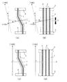
- FIG. 1 is a schematic plan view showing the relationship between wiring formed of a copper foil layer of a flexible circuit board and a ridge line of a bent portion.
- FIG. 2 is an explanatory cross-sectional view showing a state in which the flexible circuit board is bent.
- FIG. 3 is an explanatory diagram of the MIT bending test apparatus.
- FIG. 4A is an explanatory view of an IPC bending test apparatus, and
- FIG. 4B is an XX ′ sectional view of a test flexible circuit board used in the IPC bending test.
- FIG. 5 is a perspective explanatory view of a single-sided copper-clad laminate.
- the copper foil of the present invention is less susceptible to fatigue breakage against repeated loads (loads) and strains, and in order to realize such a copper foil, by adopting two types of alloy compositions, Each of them is less likely to cause metal fatigue and has excellent durability against stress and strain, and has successfully obtained a copper-clad laminate and a flexible circuit board.
- the copper foil having the first alloy composition contains 0.001 mass% or more and 0.4 mass% or less of Mn as a composition, has inevitable impurities and the balance of Cu, and is a unit of copper.
- the basic orientation axis ⁇ 100> of the lattice is the area ratio of the preferentially oriented regions with an orientation difference of 15 ° or less with respect to two orthogonal axes of the thickness direction of the copper foil and a certain direction existing in the foil surface. It has a structure occupying 60% or more (hereinafter, may be referred to as “copper foil according to the first invention”). Further, the copper foil having the second alloy composition is at least one selected from the group consisting of Ca, La, Ce, Pr, Nd, Sm, Eu, Gd, Dy, Ho, Er, Tm, Yb, and Y.
- the crystal orientation ⁇ 100> is 60% or more in terms of area ratio with respect to two orthogonal axes of the copper foil thickness direction and a certain direction existing in the foil plane, each with an orientation difference of 15 ° or less. (Hereinafter, sometimes referred to as “copper foil according to the second invention”).
- the material structure affects the fatigue properties of the material.
- the structure is fine, the strength and elongation at break are improved, while the crystal grain boundary is a dislocation accumulation surface.
- the microscopic stress concentration at the time of deformation due to the anisotropy of each crystal grain due to the crystal grain orientation deteriorates the fatigue characteristics.
- the present invention provides a copper foil having excellent fatigue characteristics even in a high strain region exceeding a strain value of 1% where a wiring of a flexible circuit board is formed and a bent portion having a curvature radius of 2 mm or less is formed.
- the copper foil has no grain boundaries, and it is desirable that the copper foils are highly oriented and the three basic crystal axes of copper are aligned. Since the three basic crystal axes ⁇ 100> are orthogonal to each other, if two of these are determined, all axes are determined. That is, the primary crystallographic axis ⁇ 100> of the copper unit cell is preferentially oriented with an orientation difference of 15 ° or less with respect to two orthogonal axes of the thickness direction of the copper foil and a certain direction existing in the foil plane.
- the area needs to occupy 60% or more, preferably 80% or more by area ratio. In particular, it is preferable to occupy 95% or more, and more preferably 98% or more, in severe bending applications where a bending portion having a curvature radius of 0.8 mm or less is formed. .
- both the first and second copper foils according to the present invention have a main orientation in which the thickness direction of the copper foil is ⁇ 100>.
- the foil surface of the copper foil has a main orientation of ⁇ 100>. That is, these copper foils of the present invention have a ⁇ 100> orientation in the thickness direction of the foil, and a highly oriented cubic orientation in which the main orientation is the ⁇ 100> orientation perpendicular to the foil surface. It is necessary to present a called texture.
- all of the copper foils in the present invention preferably have a crystal grain size in the foil plane of 800 ⁇ m or more. It is desirable to have a structure that penetrates in the thickness direction of the foil.
- the contents of those descriptions are common to the copper foils according to the first and second inventions.
- the copper foil according to the first and second inventions may be either a rolled foil or an electrolytic foil, respectively, but preferably a rolled foil in order to obtain high orientation.
- a rolled foil in order to obtain high orientation.
- rolling conditions and heat treatment conditions specifically, rolling is performed at a large cold working rate (final compression ratio of 90% or more), strain is accumulated by work hardening, It is preferable to recrystallize by adding.
- One of the recrystallized structures of rolled copper is a cubic texture in which the ⁇ 100> direction is aligned in the thickness direction of the foil and the ⁇ 100> direction is aligned in the rolling direction.
- indices that represent the priority of texture orientation that is, the degree of orientation or accumulation, but it is based on objective data using statistical data of local three-dimensional orientation data obtained by electron diffraction. Other indicators can be used. Therefore, in order to define the texture with a three-dimensional degree of integration, it can be specified using the area ratio of the preferentially oriented region that falls within 15 ° with respect to the main orientation of the texture.
- the crystal orientation of a predetermined surface of the copper foil is determined by, for example, X-ray diffraction methods such as EBSD (Electron Back Scattering Diffraction) method, ECP (Electron Channeling Pattern) method, X-ray method such as micro Laue method, etc. It can be confirmed by a line diffraction method or the like.
- the EBSD method analyzes a crystal from a diffraction image called a pseudo Kikuchi line that is diffracted from each crystal plane generated when a focused electron beam is irradiated on the surface of a sample to be measured, and obtains orientation data and measurement points.
- the present invention in consideration of forming the wiring on the flexible circuit board, the portion where the wiring is bent It is desirable to scan the electron beam finely so as to obtain a sufficient number of points for obtaining an area ratio in an area larger than the above area, and obtain average information thereof.
- an area of about 0.005 mm 2 is selected, and 1000 points or more are measured in order to obtain an average area ratio. That's fine.
- alloy elements improve the strength of a metal by solid solution strengthening.
- most alloying elements for copper having a face-centered cubic structure reduce the stacking fault energy and facilitate the expansion of dislocations. For this reason, dislocations do not easily cross and slip during deformation, and local accumulation of dislocations easily occurs. As a result, it also has an effect of reducing fatigue characteristics during repeated deformation.
- Mn is considered to be less effective in reducing the stacking fault energy of copper compared to other alloys.
- copper containing Mn increases the elongation at break when tensile stress is applied in one direction in the foil plane.
- a copper alloy foil having a face-centered cubic crystal structure that is highly oriented and has a large elongation at break even when an alloy component is added, and repeats in one direction within the foil surface. It has been found that the fatigue characteristics are improved when tensile stress or strain is applied.
- the Mn content expresses its effect at 0.001% by mass or more, but particularly when 0.005% by mass or more is contained, It was found that the effect was increased. Moreover, the upper limit is prescribed
- the basic crystal axis ⁇ 100> of the copper unit cell has two orthogonal axes of the thickness direction of the copper foil and one direction existing in the foil plane.
- each of the preferential orientation regions having an azimuth difference of 15 ° or less has a structure occupying 60% or more in area ratio.
- a copper foil processed by rolling is heat-treated to form a recrystallized texture in which the ⁇ 100> orientation is highly oriented in the thickness direction and the rolling direction of the foil.
- the method can be adopted.
- the recrystallization temperature rises as the concentration of the alloy element is increased. The degree varies depending on the component type. Depending on the component type and concentration, recrystallization occurs, but ⁇ 100> recrystallized structure and cubic texture do not form.
- the main object of the present invention is to provide a copper foil for a flexible circuit board. Therefore, the copper foil can be recrystallized using the thermal history during the manufacturing process of the flexible circuit board, and this is advantageous in terms of cost.
- a flexible circuit board may be formed, but it is better to form a resin layer on the work-hardened copper foil, It is easy in terms of handling.
- a polyamic acid solution is applied by a casting method, and a resin layer made of polyimide by heat treatment.
- the temperature is 400 ° C. at the highest.
- the thermocompression bonding temperature is generally about 300 to 400 ° C. Therefore, since it is preferable to complete recrystallization at the temperature in these heat treatment and thermocompression bonding, it is more preferable that the Mn concentration in the composition of the cold-rolled copper foil does not exceed 0.1 mass%. Furthermore, when trying to manufacture this continuously, the heat treatment time is shortened, so that the Mn concentration of the copper foil for industrial flexible circuit boards is 0.06% by mass or less. It is more preferable at the point which can omit the annealing process of the copper foil before the lamination process of a copper foil and a polyimide.
- the electrical resistance value of copper is about 1.7 ⁇ 10 ⁇ 8 ⁇ m at room temperature.
- the copper foil forming the wiring is used for signal and power transmission, and therefore it is desirable that the electrical resistance is low. If the Mn concentration exceeds 0.1% by mass, the electrical resistance at room temperature exceeds 2.0 ⁇ 10 ⁇ 8 ⁇ m, and the IACS is less than 85%. More preferably, it does not exceed 1% by weight. Further, if the Mn concentration is 0.06% by mass or less, the electric resistance value further decreases to 1.9 ⁇ 10 ⁇ 8 ⁇ m or less, which is more preferable.
- the upper limit of the Ti content is defined by the recrystallization temperature as in the case of Mn.
- Ti has a larger effect of increasing the recrystallization temperature than Mn, and is a value at which the specified texture referred to in the present invention cannot be obtained by heat treatment at 500 ° C. for 1 hour.
- the upper limit of Ti content is 0 .2% by mass.
- it is desirable to complete recrystallization preferably at 400 ° C. or lower, and the upper limit of the Ti content in that case is desirably 0.05% by mass.
- Al has little effect on increasing the recrystallization temperature of copper, and can be added in principle up to 9% by mass, which is the maximum solid solubility limit of Al with respect to copper. If it is added beyond the range, a CuAl compound phase is easily formed. When this compound phase is formed, when strain is applied, stress concentrates in the vicinity of the CuAl compound in the copper foil, and the fatigue characteristics are significantly reduced.
- the copper foil according to the first invention contains inevitable impurities in addition to Mn, Ti and Al, but in particular, silver, iron and nickel contained as impurity elements in the raw material copper are the effects clarified in the present invention. Does not affect. However, with regard to oxygen, when a large amount of oxygen is contained as copper oxide, when stress is applied to the copper foil, stress concentration occurs in the copper oxide, so the oxygen content should be at most 0.1% by mass. It is necessary not to exceed, preferably 0.05 mass% or less, which is a level contained in general tough pitch copper, and more preferably 0.001 mass% or less, which is the oxygen impurity concentration level of oxygen-free copper. desirable.
- the content of one or more alloy elements selected from the group consisting of Ca, La, Ce, Pr, Nd, Sm, Eu, Gd, Dy, Ho, Er, Tm, Yb and Y can be added in a trace amount. Although the effect is exhibited, the effect is particularly great when the content is 0.005% by mass or more. If these elements are added in a total amount exceeding 0.4% by mass, the degree of integration of the cube orientation becomes conversely small. Further, when these elements do not dissolve in copper, when strain is applied to the copper foil, stress concentration occurs in the vicinity of the precipitated phase, which becomes a starting point of fracture. Therefore, the maximum solid solubility limit of the alloy element is 0.00. When it is less than 4% by mass, it is desirable not to exceed it.
- Ca, La, Ce, Pr, Nd, Sm, Eu, Gd, Dy, Ho, Er, Tm, Yb, and Y defined by the copper foil according to the second invention have similar chemical properties, and all are copper. There exists an effect
- the metal before refining and separating these elements is called misch metal, which is a mixture mainly composed of Ce, La, Pr, and Nd, and is relatively inexpensive. Since all the metals contained in the misch metal have the same effect, adding them as the misch metal is effective for cost reduction.
- the main purpose of the present invention is to provide a copper foil for a flexible circuit board. Therefore, the copper foil can be recrystallized using the thermal history during the manufacturing process of the copper-clad laminate or the flexible circuit board, which is advantageous in terms of cost.
- a copper-clad laminate may be obtained, but it is better to form a resin layer on the work-hardened copper foil, It is easy in terms of handling.
- the temperature at which the resin layer is formed is at most about 400 ° C. It is preferable to complete the recrystallization of the copper foil according to the invention.
- Al, Ti, Ag, Fe, Ni, Mn, Hf, Ta, B, or V is within the purity of the copper foil defined by the copper foil according to the second invention (copper content), The effect of the present invention is maintained.
- Al and Ti are one or more elements selected from the group consisting of Ca, La, Ce, Pr, Nd, Sm, Eu, Gd, Dy, Ho, Er, Tm, Yb, and Y.
- Mg has similar chemical properties to the element group defined by the copper foil according to the second invention, but its content is 0.001 in order to reduce the ⁇ 100> orientation degree. It is desirable that it is less than mass%.
- oxygen contains a large amount of oxygen as copper oxide.
- stress concentration occurs in the copper oxide. It is necessary not to exceed 0.1% by mass, preferably 0.05% by mass which is a level contained in general tough pitch copper, and more preferably 0.001% by mass which is an oxygen impurity concentration level of oxygen-free copper.
- Sulfur also has a high affinity with copper and is easily incorporated as an impurity. However, since sulfur has an action of embrittlement, it is desirable that the content be small.
- Al and Ti have high affinity with oxygen and sulfur, respectively, and when copper is dissolved and alloyed, it forms a compound with oxygen and sulfur that is harmful to bending fatigue resistance, and oxygen and sulfur are used as materials. There is also a secondary effect of going outside. Therefore, it is desirable to add a large amount of the above-described alloy element in consideration of the amount removed as a compound according to the content of oxygen and sulfur in the copper raw material.
- the contents of Ca, La, Ce, Pr, Nd, Sm, Eu, Gd, Dy, Ho, Er, Tm, Yb, Y, Al, and Ti in the copper foil according to the second invention Is defined by the heat treatment temperature at which a copper clad laminate is produced by forming a resin layer by a casting method, a hot press method, a laminating method, etc., under the condition that the copper foil can obtain a sufficient ⁇ 100> preferred orientation region.
- the thermal history applied to the copper foil is the same, it is possible to obtain an effect of improving the degree of integration of ⁇ 100> cube orientation by the above elements.
- ⁇ Copper-clad laminate, flexible circuit board> Using the copper foil according to the first invention described above or the copper foil according to the second invention, in the present invention, a resin layer is laminated on the copper foil layer made of any copper foil to form a copper-clad laminate, By etching the copper foil layer of the copper clad laminate to form a predetermined wiring, a flexible circuit board having excellent bending durability and flexibility can be obtained. It is suitable for use by forming a bent portion in at least one part of the wiring of the flexible circuit board, and particularly excellent fatigue characteristics even in a high strain region where the radius of curvature of the bent portion is 2 mm or less.
- the copper foil preferably has the structure and the component values defined in the first or second invention, and in addition, the structure shown below is preferable.
- the following content is common to the copper foil which concerns on 1st and 2nd invention, and the case where any one copper foil is used is called the copper clad laminated board which concerns on this invention, and a flexible circuit board.
- a rolled copper foil having a thickness of 5 to 18 ⁇ m is preferably used as the copper foil for forming the wiring of the flexible circuit board, preferably a thickness of 9 It is preferable to use a rolled copper foil of ⁇ 12 ⁇ m.
- the rolled copper foil is thicker than 18 ⁇ m, it becomes difficult to obtain a flexible circuit board having excellent fatigue characteristics in a high strain region where the radius of curvature is 2 mm or less.
- the thickness is less than 5 ⁇ m, handling for laminating the copper foil and the resin layer is difficult, and it is difficult to form a homogeneous copper-clad laminate.
- the rolled copper foil is preheated, and the basic crystal axis ⁇ 100> of the copper unit cell is the thickness direction of the copper foil. Recrystallized so as to occupy 60% or more of the preferential orientation region with an orientation difference of 15 ° or less with respect to two orthogonal axes with a certain direction existing in the foil plane. Or what was cold-rolled in the said thickness range may be made to recrystallize with the heat history of resin layer formation by the casting method, the lamination method, etc.
- the type of resin forming the resin layer is not particularly limited, and examples thereof include polyimide, polyamide, polyester, liquid crystal polymer, polyphenylene sulfide, polyether ether ketone, and the like. it can. Of these, polyimide and liquid crystal polymer are preferred because they exhibit good flexibility when used as a circuit board and are excellent in heat resistance.
- the thickness of the resin layer can be appropriately set according to the use, shape, etc. of the copper clad laminate, but is preferably in the range of 5 to 75 ⁇ m from the viewpoint of flexibility, and in the range of 9 to 50 ⁇ m. More preferably, the range of 10 to 30 ⁇ m is most preferable. If the thickness of the resin layer is less than 5 ⁇ m, the insulation reliability may be reduced. On the other hand, if it exceeds 75 ⁇ m, the thickness of the entire circuit board will increase when mounted on a small device as a flexible circuit board. There is a possibility that it will be too much, and a decrease in flexibility may be considered.
- a cover material as shown below may be formed on the wiring formed from the copper foil layer.
- the configuration of the cover material and the resin layer in consideration of the balance of stress applied to the wiring. According to the knowledge of the present inventors, for example, if the polyimide resin forming the resin layer has a tensile elastic modulus of 4 to 6 GPa at 25 ° C.
- the cover material to be used is A structure having two layers of an adhesive layer made of a thermosetting resin having a thickness of 8 to 17 ⁇ m and a polyimide layer having a thickness of 7 to 13 ⁇ m, and the tensile elastic modulus of the entire adhesive layer and the polyimide layer being 2 to 4 GPa Is desirable.
- the polyimide forming the resin layer has a tensile modulus of 6 to 8 GPa at 25 ° C. and a thickness in the range of 12 to 15 ⁇ m
- the cover material to be used is made of a thermosetting resin having a thickness of 8 to 17 ⁇ m. It is desirable that the adhesive layer and the polyimide layer having a thickness of 7 to 13 ⁇ m have two layers, and the tensile elastic modulus of the adhesive layer and the entire polyimide layer is 2 to 4 GPa.
- the copper foil may be thermally laminated by applying or interposing a thermoplastic polyimide to the polyimide film (so-called “so-called”). Laminating method).
- the polyimide film used in the laminating method include “Kapton” (Toray DuPont Co., Ltd.), “Apical” (Kanebuchi Chemical Industry Co., Ltd.), “Upilex” (Ube Industries Co., Ltd.), and the like.
- the polyimide film and the copper foil are thermocompression bonded, it is preferable to interpose a thermoplastic polyimide resin exhibiting thermoplasticity.
- thermocompression bonding temperature is preferably 280 ° C. or more and 400 ° C. or less, and preferably 300 ° C. or more and 400 ° C. or less. good.
- the temperature of the heat treatment for imidizing the polyimide precursor solution to form the resin layer is preferably 280 ° C. or higher and 400 ° C. or lower, preferably 300 ° C. or higher and 400 ° C. or lower. Is good.
- the resin layer may be formed by laminating a plurality of resins.
- two or more kinds of polyimides having different linear expansion coefficients may be laminated, and in that case, heat resistance and flexibility are ensured.
- the tensile elastic modulus of the resin layer is preferably 4 to 10 GPa, preferably 5 to 8 GPa, including the case of being composed of a single polyimide and the case of being composed of a plurality of polyimides.
- the linear expansion coefficient of the resin layer be in the range of 10 to 30 ppm / ° C.
- the linear expansion coefficient of the entire resin layer may be in this range.
- a low linear expansion polyimide (low thermal expansion polyimide) layer having a linear expansion coefficient of 25 ppm / ° C. or less, preferably 5 to 20 ppm / ° C., and a linear expansion coefficient of 26 ppm / ° C.
- a resin layer comprising a high linear expansion polyimide (high thermal expansion polyimide) layer of 30 to 80 ppm / ° C., and the thickness of the resin layer is adjusted to 10 to 30 ppm / ° C. Can do.
- a preferred ratio of the thickness of the low linear expansion polyimide layer to the high linear expansion polyimide layer is in the range of 70:30 to 95: 5.
- the low linear expansion polyimide layer is the main resin layer of the resin layer, and the high linear expansion polyimide layer is preferably provided in contact with the copper foil.
- the linear expansion coefficient was determined by using a polyimide whose imidization reaction was sufficiently completed as a sample, raising the temperature to 250 ° C. using a thermomechanical analyzer (TMA), cooling at a rate of 10 ° C./min, and 240 to 100 ° C. It can obtain
- TMA thermomechanical analyzer
- the flexible circuit board obtained from the copper-clad laminate in the present invention includes a resin layer and a wiring formed from a copper foil layer, and is used with a bent portion in one of them.
- it is widely used in various electronic and electrical devices such as movable parts in hard disks, hinges and slides of mobile phones, printer heads, optical pickups, movable parts of notebook PCs, etc., and the circuit board itself Is bent, twisted, or deformed according to the operation of the mounted device, and a bent portion is formed in either of them.
- the flexible circuit board of the present invention since the flexible circuit board of the present invention has a bent portion structure with excellent bending durability, it is frequently accompanied by repeated operations such as sliding bending, bending bending (including goby folding), hinge bending, and sliding bending.
- the radius of curvature is 0.38 to 2.0 mm in the bending behavior and 1.25 to 2.0 mm in the sliding bending in order to cope with the size reduction of the equipment to be bent or mounted.
- Suitable for harsh conditions such as hinge bending 3.0 to 5.0 mm and slide bending 0.3 to 2.0 mm, and requires bending performance with a narrow gap of 0.3 to 1 mm Is particularly effective in slide applications where the bending radius is 0.8 mm or less, and particularly in such a bending application where a bending portion having a curvature radius of 0.8 mm or less is formed.
- FIG. 1 shows a flexible circuit board used for, for example, a hinge part of a cellular phone, and is an example having a resin layer 1, a wiring 2 formed from a copper foil, and a connector terminal 3.
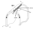
- FIG. 2 shows a schematic diagram when the flexible circuit board of FIG. 1 is bent into a U shape so that a ridge line L is formed. As shown in FIG.
- FIG. 1A is an example in which the wiring is formed obliquely in the vicinity of the ridge line L in the middle of the connector terminals 3 at both ends.
- FIG. Wiring is also possible.
- the slide sliding bend in which the ridge line L in the bent portion moves as in a slide type mobile phone may be the direction of the thick arrow.
- the flexible circuit board in this invention is equipped with the wiring which consists of copper foils on at least one surface of a resin layer, you may make it equip both surfaces of a resin layer with copper foil as needed.
- the wiring 2 formed from the copper foil in the flexible circuit board of the present invention may be oriented in any direction.
- ⁇ ° can take any angle. That is, in the flexible circuit board of the present invention, one ⁇ 100> axis of the preferentially oriented region in the copper wiring is the thickness direction of the copper foil and is perpendicular to the resin layer 1, but the other two The two ⁇ 100> axes may be oriented in any direction within the copper wiring plane. Further, when the flexible circuit board shown in FIG. 1 is bent in a U-shape so as to form a ridge line L and a fatigue test is performed, the [100] axis in FIG. FIG. 1C and FIG. 1D are the most severe directions. This is due to the following reason.
- the main stress applied to the copper circuit depends on the configuration of the flexible circuit board, but the ridge line L is a tensile perpendicular to the cross section that cuts the copper wiring, Or it is compressive stress. If the cross-sectional orientation of the wiring when cutting in the thickness direction from the ridgeline at the bent portion is (100), the eight Schmitt factors of the eight slip surfaces are equivalent when the bend is made, and the eight slip systems work at the same time. Dislocations are easy to accumulate. As shown in FIGS.
- Schmidt when the angle between the [100] axis and the ridge line L is set to an angle other than 90 °, Schmidt is one of the eight ⁇ 111 ⁇ that are the sliding surfaces of the copper foil. Since the main slip surface having the largest factor is four, the shear slip is good and local work hardening is difficult to occur.
- the longitudinal direction of the copper foil corresponds to the rolling direction, and a circuit is formed along the main direction ⁇ 100> as shown in FIGS. 1 (c) and (d). It is normal to do.
- a circuit is formed in such a direction using a conventional copper foil, there is a problem in durability.
- the present invention hardly breaks against repeated bending.
- a copper foil wiring is formed as shown in FIGS. 1A and 1B, a flexible circuit board having higher bending fatigue characteristics is obtained.
- the copper foil of the present invention is highly oriented and contains a specified alloy component, so that metal fatigue hardly occurs and has excellent durability against stress and strain.
- a flexible circuit board obtained by forming a copper clad laminate using such a copper foil and etching the copper foil by a known method to form a wiring is not repeatedly bent or curved. Since it has strength that can withstand bending with a small radius and is excellent in flexibility, there is no restriction on the design of the flexible circuit board such as considering the shape of the wiring in the bent portion.
- Example 1 In this example, a copper foil having Mn as an alloy element was prepared, and the elongation at break was measured from a test single-sided copper-clad laminate using the same, and the test was possible from the test single-sided copper-clad laminate. A flexible circuit board was prepared and the bending fatigue characteristics were measured.
- the copper foils according to sample numbers 1 to 16 used in this example were manufactured as follows. An oxygen-free copper having a purity of 99.99% and an oxygen content of 0.0008% and Mn having a purity of 99.9% weighed to a predetermined amount as shown in Table 1 in a graphite crucible in an argon atmosphere It was dissolved and stirred, and poured into a rectangular parallelepiped graphite mold having a width of 50 mm, a length of 100 mm, and a thickness of 15 mm to produce an ingot.
- tentering was performed so that the thickness became 10 mm in the width direction, hot rolling was performed at a maximum of 600 ° C., and further hot rolling was performed in the length direction up to a thickness of 2 mm under the same conditions. Thereafter, cold rolling was performed until the thickness reached 9 ⁇ m. Meanwhile, both ends were cut by slitting at a thickness of 0.5 mm, and the width was adjusted to 60 mm. Therefore, the obtained copper foil had a width of 60 mm and a thickness of 9 ⁇ m.
- polyamic acid solutions which are polyimide precursors constituting the resin layer of the test flexible circuit board according to Example 1, were synthesized by the following method.
- the polyamic acid solution a prepared above is applied to the surfaces of the copper foils according to Sample Nos. 1 to 16 prepared above and dried (after curing, a 2 ⁇ m-thick thermoplastic polyimide film is formed), and a polyamide is formed thereon.
- a resin layer made of polyimide having a three-layer structure was formed through heat treatment under a heating condition where the maximum temperature was 400 ° C. and the cumulative time in the temperature range of 360 to 400 ° C. was 5 minutes.
- a resin layer (polyimide) having a thickness of 13 ⁇ m was cut out to have a rectangular size of 250 mm in length along the rolling direction (MD direction) of the copper foil and 40 mm in width in the direction orthogonal to the rolling direction (TD direction).
- MD direction rolling direction
- TD direction rolling direction
- a test single-sided copper-clad laminate having 1 and a copper foil layer 2 having a thickness of 9 ⁇ m was obtained (FIG. 5). At that time, the tensile elastic modulus of the entire resin layer was 7.5 GPa.
- the elongation at break of the copper foil is 150 mm long in the rolling direction of the copper foil obtained by chemically removing the polyimide resin layer of the single-sided copper clad laminate for testing, and the direction perpendicular to the rolling direction in the foil surface.
- a specimen cut into a width of 10 mm was used, and the distance between gauge points was 100 mm in the length direction, and the tensile speed was 10 mm / min. Obtained by measurement. For the measurement, seven samples were prepared for each type of copper foil, and the average value of elongation at break was determined.
- the structure of the copper foil was obtained by performing orientation analysis using an EBSD device after mechanical and chemical polishing using colloidal silica on the rolled surface of each copper foil.
- the devices used were FE-SEM (S-4100) manufactured by Hitachi, Ltd., EBSD device manufactured by TSL, and software (OIM Analysis 5.2).
- the measurement area was an area of approximately 800 ⁇ m ⁇ 1600 ⁇ m, and the measurement acceleration voltage was 20 kV and the measurement step interval was 4 ⁇ m. That is, the number of measurement points is 80000 points.
- the degree of integration of the cube texture of the present invention that is, the evaluation of the ⁇ 100> preferential orientation region is measured at a point where ⁇ 100> is within 15 ° with respect to both the thickness direction of the foil and the rolling direction of the foil. Can be expressed as a percentage of the total measurement points. The number of measurements was made on five different samples of each variety and rounded to the nearest whole number. In addition, using the obtained data, the crystal grain size was evaluated using a crystal grain boundary that has an orientation difference of 15 ° or more between adjacent crystal grains.
- a predetermined mask is put on the copper foil layer side of the single-sided copper clad laminate for test obtained above, and etching is performed using an iron chloride / copper chloride solution, and a straight line having a line width (l) of 150 ⁇ m.
- the wiring pattern was formed so that the wiring direction of the shaped wiring was parallel to the rolling direction and the space width was 250 ⁇ m.
- JIS 6471 for testing having a width of 150 mm in the longitudinal direction along the wiring direction H of the circuit board and a width of 40 mm in the direction orthogonal to the wiring direction H A flexible circuit board was obtained. It was confirmed that there was no change in the structure of the copper foil before and after circuit formation by etching.
- MIT flex test was performed according to JIS C5016.
- a schematic diagram of the test is shown in FIG.
- the equipment is manufactured by Toyo Seiki Seisakusho (STROGRAPH-R1), one end in the longitudinal direction of the flexible circuit board for testing is fixed to the holding jig of the bending test apparatus, and the other end is fixed with a weight.
- the curvature radius is 0.8 mm while alternately rotating left and right by 135 ⁇ 5 degrees at a vibration speed of 150 times / min. The number of times was determined as the number of flexions.
- the main stress applied to the copper circuit and the main strain are applied because the ridgeline formed in the bent portion is bent so as to be orthogonal to the wiring direction H of the wiring of the test flexible circuit board. Becomes tensile stress and tensile strain parallel to the rolling direction.
- the circuit was observed from the thickness direction of the copper foil after the bending test, it was confirmed that a crack occurred in the vicinity of the ridgeline of the bent portion, almost perpendicular to the rolling direction, and a broken line.
- Table 1 shows the amount of Mn in the copper foil obtained by the test described above, the elongation at break of the copper foil, the ⁇ 100> preferred orientation area ratio, and the bending life.
- the bending life is an average of the results of the test flexible circuit boards prepared for each of the copper foil types.
- Mn increases the breaking elongation in the length direction of the wiring, which is the main stress direction during bending, that is, in the rolling direction.
- Mn concentration 0.001% by mass or more
- crystal grains having a cubic orientation have grown to a size of 800 ⁇ m or more in the copper foil plane and penetrated in the thickness direction of the foil. It was.
- the bending resistance of the No. 11 sample is relatively high, whereas the number of times until the No. 12 sample breaks. was small. This is because the sample No. 11 copper foil was subjected to recrystallization heat treatment at 500 ° C. for 1 hour, so that recrystallization proceeded and the area ratio of the ⁇ 100> preferred orientation region was relatively large. by.
- the area ratio of the ⁇ 100> preferred orientation region is 60% or less regardless of whether recrystallization heat treatment was performed before forming the flexible circuit board.
- the number of bendings until the breakage was greatly reduced. This is because the recrystallization temperature increased due to the excessive addition of Mn.
- the polyimide formation time in this example is 5 minutes, which is a test simulating continuous production of roll-to-roll. Comparing samples that had not been subjected to recrystallization heat treatment at 500 ° C. for 1 hour in advance, the bending life was increased when the Mn concentration was 0.005 mass% or more and 0.06 mass% or less. That is, the copper foil in this concentration range is particularly suitable as a copper foil used when obtaining a polyimide-based flexible circuit board having a resin layer made of polyimide.
- Example 2 In this example, a copper foil having Mn, Ti, and Al as alloy elements was prepared, and the elongation at break was measured from a test single-sided copper-clad laminate using the same. From the test single-sided copper-clad laminate, A flexible circuit board for testing was prepared and the bending fatigue characteristics were measured.
- the copper foils according to sample numbers 17 to 38 used in this example were produced as follows. As shown in Table 2, a tough pitch copper having a purity of 99.9% and an oxygen content of 0.015% and Mn, Ti, and Al having a purity of 99.9% each weighed to a predetermined amount, as shown in Table 2. The mixture was stirred in an argon atmosphere and poured into a rectangular graphite mold having a width of 50 mm, a length of 100 mm, and a thickness of 15 mm to produce an ingot. Thereafter, tenter rolling was performed so that the thickness became 10 mm in the width direction, hot rolling was performed at a maximum of 600 ° C., and further hot rolling was performed under the same conditions in the length direction to a thickness of 2 mm.
- the obtained copper foil had a width of 60 mm and a thickness of 12 ⁇ m.
- the polyamic acid solution a was applied to the surface of the copper foil according to Test Nos. 17 to 38 prepared above. Is applied and dried (after forming a 2 ⁇ m-thick thermoplastic polyimide film after curing), then coated with polyamic acid b and dried (after curing, a 8 ⁇ m-thick low thermal expansion polyimide film is formed), and further The polyamic acid a is applied and dried (after forming a 2 ⁇ m-thick thermoplastic polyimide film after curing), the maximum temperature is 400 ° C., and the total time in the temperature range of 360 to 400 ° C. is 5 minutes. Through a heat treatment under heating conditions, a resin layer made of polyimide having a three-layer structure was formed.
- the resin layer (polyimide) having a thickness of 12 ⁇ m and the copper foil having a thickness of 12 ⁇ m are cut out to have a rectangular size of 250 mm in length along the rolling direction of the copper foil and a width of 40 mm in a direction orthogonal to the rolling direction.
- a test single-sided copper clad laminate according to Example 2 having a layer was obtained.
- the cover material 7 (Arisawa Seisakusho CVK-0515KA: thickness 12.5 ⁇ m) was laminated.
- the thickness of the adhesive layer 6 made of an adhesive was 15 ⁇ m in a portion without a copper foil circuit, and 6 ⁇ m in a portion where a copper foil circuit was present. And it cut out so that it might become 15 cm in a length direction along a wiring direction (H direction), and 8 mm in the direction orthogonal to a wiring direction, and the flexible circuit board for a test for setting it as an IPC test sample was obtained.
- the IPC test is a test simulating slide bending, which is one of the bending forms used for mobile phones and the like, as shown schematically in FIG.
- the IPC test is a test in which a bent portion is provided with a determined gap length 8 as shown in FIG. 4, one side is fixed by a fixing portion 9, and the slide operating portion 10 on the opposite side is repeatedly reciprocated as shown in the drawing. . Therefore, the substrate is repeatedly bent in a region corresponding to the stroke amount of the reciprocating portion.
- the test was performed by repeatedly sliding the resin layer (polyimide) 1 with the cap length being 1 mm, that is, the bending radius being 0.5 mm and the stroke being 38 mm.
- the electrical resistance of the circuit of the test flexible circuit board was measured, and the progress of fatigue cracks in the copper foil circuit was monitored by increasing the electrical resistance.
- the circuit breakage life was defined as the number of strokes at which the electrical resistance of the circuit reached twice the initial value.
- the ridgeline formed in the bent portion is bent so as to be orthogonal to the wiring direction of the wiring 2 of the test flexible circuit board, so that the main stress and the main strain applied to the copper circuit are The tensile stress and tensile strain are parallel to the rolling direction.
- Table 2 shows the results of the Mn, Ti, and Al contents in the copper foil obtained by the test described above, the elongation at break of the copper foil, the ⁇ 100> preferred orientation area ratio, and the bending life.
- Example 3 The copper foil used in this example was manufactured as follows. As a raw material, oxygen-free copper having a plate thickness of 15 mm, a purity of 99.99% or more and an oxygen content of 0.0008% was used. The raw copper and each alloy element weighed to a predetermined concentration are dissolved in an argon atmosphere in a graphite crucible and stirred to form a rectangular graphite mold having a width of 50 mm, a length of 100 mm, and a thickness of 15 mm. An ingot was produced by pouring. Among the alloying elements, the purity of yttrium, calcium, and ytterbium is 99.9% or more. Misch metal was also used as the alloying element. The main components of misch metal are La 25% by mass, Ce 53% by mass, Pr 6% by mass and Nd 15% by mass. The total purity of these elements is 99% by mass, and the balance is Other inevitable impurities including other rare earth metals.
- the cast ingot is tentered to a thickness of 10 mm in the width direction, hot-rolled at a maximum of 600 ° C., and further hot-rolled under the same conditions in the length direction to a thickness of 1.5 mm. went.
- a raw copper plate was directly cut into the same size as a cast ingot and hot-rolled under the same conditions. Thereafter, these hot-rolled sheets were cold-rolled to a thickness of 9 ⁇ m. Meanwhile, both ends were cut by slitting at a thickness of 0.5 mm, and the width was adjusted to 60 mm. Therefore, the obtained copper foil had a width of 60 mm and a thickness of 9 ⁇ m.
- a comparative material prepared by the same process was prepared by melting and casting without adding an alloy element.
- Table 3 summarizes the alloy concentrations of the copper foils (sample numbers 39 to 70) used in this example.
- the copper content is a calculated value determined as follows from the analyzed alloying elements and the amount of impurities derived from the raw materials, and is a theoretical range.
- the lower limit value of the copper content shown in Table 3 was obtained from “(minimum value of raw material purity) ⁇ (alloy element content) ⁇ (impurities derived from alloy elements)”.
- the upper limit value was obtained from “100 ⁇ (alloy element content)”.
- the polyamic acid solution which is a polyimide precursor constituting the resin layer of the test flexible circuit board of this example, was obtained according to the two synthesis examples described in Example 1.
- the resulting polyamic acid b is applied and dried (forms a low thermal expansion polyimide with a film thickness of 9 ⁇ m after curing), and further coated with polyamic acid a and dried (a thermoplastic polyimide with a film thickness of 2 ⁇ m after curing)
- a resin layer made of polyimide having a three-layer structure was formed through heating conditions such that a temperature of 280 ° C. or 350 ° C. was loaded for 5 minutes or more in an integrated time.
- this heat processing temperature be a polyimide formation temperature.
- a resin layer (polyimide) having a thickness of 13 ⁇ m was cut out to have a rectangular size of 250 mm in length along the rolling direction (MD direction) of the copper foil and 40 mm in width in the direction orthogonal to the rolling direction (TD direction).
- MD direction rolling direction
- TD direction rolling direction
- a test single-sided copper-clad laminate having 1 and a copper foil layer 2 having a thickness of 9 ⁇ m was obtained (FIG. 5). At that time, the tensile elastic modulus of the entire resin layer was 7.5 GPa.
- Example 2 The structure of the copper foil (copper foil layer) in the single-sided copper clad laminate obtained above was analyzed in the same manner as in Example 1. Further, a predetermined mask was placed on the copper foil side of the test single-sided copper clad laminate obtained above, and etching was performed using an iron chloride / copper chloride solution to form a wiring pattern similar to that in Example 1. . And in accordance with JIS 6471, a flexible test device having a length of 150 mm in the longitudinal direction along the wiring direction H of the circuit board and a width of 40 mm in the direction perpendicular to the wiring direction H so as to serve also as a sample for bending resistance test. A circuit board was obtained. It was confirmed that there was no change in the structure of the copper foil before and after circuit formation by etching.
- Table 3 shows the alloy element amount, ⁇ 100> preferred orientation area ratio, and bending life in the copper foil obtained by the test described above, together with the sample number and polyimide formation temperature.
- the bending life is an average of the results of the test flexible circuit boards prepared for each of the copper foil types.
- a component value of “ ⁇ ” indicates that it is below the measurement limit value of chemical analysis.
- 1 was selected from the group consisting of Ca, La, Ce, Pr, Nd, Yb and Y as compared with the copper foil prepared without adding any alloying element. It can be seen that by including seeds or more in an amount of 0.005% by mass or more and 0.4% by mass or less, the area ratio of the ⁇ 100> preferred orientation region was increased when compared at the same heat treatment temperature, and fatigue life was reduced. Improved. In addition to Ca and Y, an effect was also seen in La having a large metal radius in the lanthanoid genus and the smallest Yb, so that the chemical characteristics are similar, and Sm, Eu, It can be determined that Gd, Dy, Ho, Er, and Tm have the same effect.
- the area ratio of the ⁇ 100> preferred orientation region of the copper foil varies greatly depending on the temperature at which the test single-sided copper-clad laminate is formed, that is, the polyimide formation temperature in this example, but the thermal history at 280 ° C. for 5 minutes.
- the area ratio of the ⁇ 100> preferentially oriented region is 60% or more, and ⁇ 100> preferential compared to the copper foil prepared without adding the alloy element. It was found that both the area ratio of the orientation region and the fatigue life were exceeded.
- 0.4% by mass of Ca was added in sample numbers 52 to 54 (sample number 54)
- the area ratio of the ⁇ 100> preferred orientation region decreased because the recrystallization temperature increased due to the addition of alloy elements. This is probably because the formation of ⁇ 100> recrystallized texture was inhibited.
- Example 4 In this example, a miscible metal, Ti, and Al are used to produce a copper foil having these as alloy elements, and the copper foil structure is analyzed from the test single-sided copper-clad laminate obtained using the same, A test flexible circuit board was prepared from the test single-sided copper-clad laminate, and the bending fatigue characteristics were measured.
- the main components of misch metal used in this example are La 25% by mass, Ce 54% by mass, Pr 6% by mass, Nd 14% by mass, and the total purity of these elements is 99% by mass. Other components are other inevitable impurities including other rare earth metals.
- the copper foil used in this example was manufactured as follows. An electrolytic copper plate having a thickness of 15 mm and a purity of 99.9% or more, an oxygen content of 0.015% by mass, a sulfur content of 0.03% by mass, and a silver content of 0.02%, and a predetermined amount The Ti and Al alloy elements having a purity of 99.9% or more, and the constituent elements and misch metal having the purity were weighed to a predetermined concentration, dissolved in an argon atmosphere in a graphite crucible, stirred, An ingot was produced by pouring into a rectangular graphite mold having a width of 50 mm, a length of 100 mm, and a thickness of 15 mm.
- the cast ingot was rolled out to a thickness of 10 mm in the width direction, hot-rolled at a maximum of 600 ° C., and further hot-rolled under the same conditions in the length direction to a thickness of 1 mm. . Thereafter, cold rolling was performed until the thickness became 12 ⁇ m. Meanwhile, both ends were cut by slitting at a thickness of 0.5 mm, and the width was adjusted to 60 mm. Therefore, the obtained copper foil was 60 mm in width and 12 ⁇ m. Further, a comparative material prepared by the same process was prepared by melting and casting without adding an alloy element.
- Table 4 summarizes the alloy concentrations of the copper foils (sample numbers 71 to 84) used in this example.
- the copper content is a calculated value obtained from the analyzed alloying element and the amount of impurities in the raw material, and is in a theoretical range.
- the upper limit value of the copper content was calculated as a case where other impurities were gas components and the like, and all of them were discharged out of the system by reaction with gas or rare earth elements in the process of alloying.
- the lower limit was calculated assuming that all impurities in the raw material remained in the alloy. That is, the content of alloy elements excluding silver is subtracted from the lower limit of the purity of the raw material copper, and 1% other than La, Ce, Pr, and Nd in the rare earth elements is other than the elements shown in Table 4, Was subtracted assuming that 0.1% of impurities of Al and Ti remained as well.
- Silver was not added as an alloy element, but was mainly mixed as an impurity in the raw material copper, and was added to the subtracted value.
- the polyamic acid solution a prepared by the same method as in Synthesis Example 1 of Example 1 is applied and dried (after curing, a 2 ⁇ m-thick thermoplastic polyimide film is formed), and then Synthesis Example of Example 1 is formed thereon.
- the polyamic acid b prepared in the same manner as in No. 2 was applied and dried (after curing, a low thermal expansion polyimide film having a thickness of 8 ⁇ m was formed), and then the polyamic acid a was further applied and dried (after curing, the film was cured)
- a polyimide layer (resin layer) was formed through heating conditions in which a thermoplastic polyimide having a thickness of 2 ⁇ m was formed) and a temperature of a maximum temperature of 320 ° C. was added for an integrated time of 10 minutes.
- a polyimide layer (resin 12 ⁇ m thick) is cut out to have a rectangular size of 250 mm in length along the rolling direction (MD direction) of the copper foil and a width of 40 mm in the direction orthogonal to the rolling direction (TD direction).
- Example 2 The structure of the copper foil (copper foil layer) in the single-sided copper clad laminate obtained above was analyzed in the same manner as in Example 1. Moreover, a predetermined mask was put on the copper foil layer side of the single-sided copper clad laminate for test, and etching was performed using an iron chloride / copper chloride solution to form a wiring pattern similar to that in Example 1. And in order to serve as a sample for bending resistance test described later, in accordance with JIS 6471, for testing having a width of 150 mm in the longitudinal direction along the wiring direction H of the circuit board and a width of 40 mm in the direction orthogonal to the wiring direction H A flexible circuit board was obtained. It was confirmed that there was no change in the structure of the copper foil before and after circuit formation by etching.
- the cover material 7 (Arisawa Seisakusho CVK-0515KA: thickness 12.5 ⁇ m) was laminated.
- the thickness of the adhesive layer 6 made of an adhesive was 15 ⁇ m in a portion without a copper foil circuit, and 6 ⁇ m in a portion where a copper foil circuit was present. And it cut out so that it might become 15 cm in a length direction along a wiring direction (H direction), and 8 mm in the direction orthogonal to a wiring direction, and the flexible circuit board for a test for setting it as an IPC test sample was obtained.
- Example 2 An IPC test was performed in the same manner as in Example 2, and the number of strokes at which the electrical resistance of the circuit reached twice the initial value was determined as the circuit breakage life.
- the circuit breakage life about the copper foil after a circuit fracture life, when the cross section which cut the copper foil in the thickness direction so as to be orthogonal to the sliding direction is observed with a scanning electron microscope, there is a difference in degree as in Example 2.
- Table 4 shows the alloy component values, ⁇ 100> preferred orientation area ratio, and flex life in the copper foil obtained by the tests described above, together with the sample number and polyimide formation temperature.
- a component value of “ ⁇ ” indicates that it is below the measurement limit value of chemical analysis. Since the raw material copper used in this example had a relatively low purity, a relatively large amount of Ag was detected in the copper foil in addition to the added alloy element. In addition, oxygen and sulfur were detected as other inevitable impurities.
- the area ratio of the ⁇ 100> preferred orientation region of the copper foil and the IPC test were compared with the case where no miscible metal or alloy element was added. It can be seen that the measured fatigue life is high.
- the concentration increases within the range defined by the present invention, and the ⁇ 100> priority orientation region is increased. It can be seen that the fatigue rate measured by the area ratio and the IPC test is high.
- the fatigue life of the sample No. 76 added with 0.41% by mass of Al and the sample No. 81 added with 0.21% by mass of Ti were conversely reduced. This is considered to be because the excessive addition of alloying elements increases the recrystallization temperature and inhibits the formation of the ⁇ 100> recrystallization texture.
- Example 5 these copper alloy foils were produced using Ce, La, Y, Sm, Ca, and Al as alloy elements, and the copper foils were obtained from the test single-sided copper clad laminate obtained using the alloy foils. While analyzing the structure
- the purity of the alloy elements used in this example is 99.9% or more, and each has a granular shape of 2 to 3 mm.
- the copper foil used in this example was manufactured as follows.
- the raw material copper is tough pitch copper having a diameter of 5 mm and a length of about 20 mm, and has a purity of 99.96% and an oxygen content of 0.029% by mass.
- the charged composition (weighed composition) to be charged before the alloy element was dissolved was fixed at 0.01%. That is, the sample No. 89 shown in Table 5 below has 99.8% of the raw material copper, 0.1% of Ce, and 0.1% of Al.
- the raw copper and alloy elements were melted and cast by the following two methods.
- One is that the alloy element wrapped in the copper foil obtained by rolling the raw copper in advance is put in a crucible, and once evacuated in a vacuum furnace, 99.99% argon is introduced and controlled to 1 atm. After melting at 1200 ° C. and stirring in an argon atmosphere, it was poured into a rectangular graphite mold having a width of 50 mm, a length of 100 mm, and a thickness of 15 mm in the furnace to produce an ingot. The produced ingot was subjected to ultrasonic cleaning in a pickling solution obtained by adding 20% hydrochloric acid and 0.1% hydrogen peroxide solution to pure water, and the surface scale was removed.
- the alloy element wrapped in copper foil rolled from raw copper is put in a crucible, melted at 1200 ° C. while introducing 99.99% argon into the box furnace, taken out of the crucible, An ingot was produced by pouring into a rectangular graphite mold having a width of 50 mm, a length of 100 mm, and a thickness of 15 mm. The produced ingot was subjected to ultrasonic cleaning in a pickling solution obtained by adding 20% hydrochloric acid and 0.1% hydrogen peroxide solution to pure water, and the surface scale was removed.
- the subsequent ingot processing methods were the same regardless of the casting atmosphere as described above.
- the ingot was rolled out to a thickness of 10 mm in the width direction, hot-rolled at a maximum of 600 ° C., and further hot-rolled under the same conditions in the length direction to a thickness of 1 mm. Thereafter, cold rolling was performed until the thickness became 12 ⁇ m. Meanwhile, both ends were cut by slitting at a thickness of 0.5 mm, and the width was adjusted to 60 mm. Therefore, the obtained copper foil was 60 mm in width and 12 ⁇ m. Further, a comparative material prepared by the same process was prepared by melting and casting without adding an alloy element.
- the copper content is a calculated value obtained from the analyzed element and the amount of impurities in the raw material, and is in a theoretical range.
- the analytical value of the alloy element is smaller than 0.1%, as shown by the result of sample number 89, for example. This is mainly due to oxygen and sulfur contained in impurities, and in the atmosphere during melting and casting. It reacts with oxygen to form oxides or sulfides, which are discharged to the upper part of the ingot and the surface layer part, and come out of the system as a scale during pickling. Although a small and small deoxidation effect was also observed in aluminum, it is considered that the rare earth element was larger under the present conditions.
- the polyamic acid solution a prepared by the same method as in Synthesis Example 1 of Example 1 is applied and dried (after curing, a 2 ⁇ m-thick thermoplastic polyimide film is formed), and then Synthesis Example of Example 1 is formed thereon.
- the polyamic acid b prepared in the same manner as in No. 2 was applied and dried (after curing, a low thermal expansion polyimide film having a thickness of 8 ⁇ m was formed), and then the polyamic acid a was further applied and dried (after curing, the film was cured)
- a polyimide layer (resin layer) was formed through heating conditions such that a 2 ⁇ m-thick thermoplastic polyimide was formed) and a maximum temperature of 360 ° C. was added for 10 minutes over an integrated time.
- a polyimide layer (resin 12 ⁇ m thick) is cut out to have a rectangular size of 250 mm in length along the rolling direction (MD direction) of the copper foil and a width of 40 mm in the direction orthogonal to the rolling direction (TD direction).
- Example 2 The structure of the copper foil (copper foil layer) in the single-sided copper clad laminate obtained above was analyzed in the same manner as in Example 1. Moreover, a predetermined mask was put on the copper foil layer side of the single-sided copper clad laminate for test, and etching was performed using an iron chloride / copper chloride solution to form a wiring pattern similar to that in Example 1. And in order to serve as a sample for bending resistance test described later, in accordance with JIS 6471, for testing having a width of 150 mm in the longitudinal direction along the wiring direction H of the circuit board and a width of 40 mm in the direction orthogonal to the wiring direction H A flexible circuit board was obtained. It was confirmed that there was no change in the structure of the copper foil before and after circuit formation by etching.
- the test flexible circuit board having the resin layer 1 and the wiring (copper foil) 2 was obtained in the same manner as in Example 2 to obtain an IPC test sample.
- the IPC test was performed in the same manner as in Example 2 except that the polyimide layer (resin layer) 1 was the outside, the cap length was 1.5 mm, that is, the bending radius was 0.75 mm, and the stroke was 38 mm.
- the number of strokes at which the electrical resistance of the circuit reached twice the initial value was determined as the circuit breakage life.
- the copper foil after a circuit fracture life when the cross section which cut the copper foil in the thickness direction so as to be orthogonal to the sliding direction is observed with a scanning electron microscope, there is a difference in degree as in Example 2. However, it was observed that cracks were generated on the surfaces of the copper foils on the resin layer side and the cover material side, and in particular, many cracks were introduced on the surface of the copper foil on the resin layer side that is outside the bent portion. .
- Table 5 shows the alloy component values, ⁇ 100> preferred orientation area ratio, and flex life in the copper foil obtained by the tests described above together with the sample number and polyimide formation temperature.
- a component value indicated by “ ⁇ ” indicates that it has not been measured.
- the oxygen concentration of the copper foil of the one cast and melted in the Ar stream is smaller than that of the raw material copper. This is a deoxidation effect due to melting and casting at a low oxygen concentration.
- Samples Nos. 87, 91, 94, and 96 were obtained by adding Ce, Y, Sm, and Ca, and melting and casting under the same conditions, but by adding these elements, ⁇ 100> has priority.
- sample number 86 the one cast in the atmosphere has a higher oxygen concentration in the copper foil than in the raw material copper.
- sample numbers 88, 90, 92, and 96 it can be seen that the oxygen concentration in the copper foil is decreased by adding Ce, La, Y, and Ca. This is because these elements have a deoxidizing effect.
- the fatigue life measured by the IPC test in these samples is high because of the direct effect that the rare earth element improves the area ratio of the ⁇ 100> preferred orientation region and the deoxidation effect due to the oxidation reaction during melting and casting. It is considered a thing.
- the results of sample numbers 89, 93, and 98 are considered to indicate that aluminum further enhances the effect.
- the copper foil of the present invention can be widely used as a flexible circuit board in various electronic and electrical devices, and the circuit board itself is bent, twisted, or deformed according to the operation of the mounted device. In other words, it is suitable for use with a bent portion in any one of them.
- the flexible circuit board of the present invention since the flexible circuit board of the present invention has a bent portion structure with excellent bending durability, it is frequently bent with repeated operations such as sliding bending, bending bending, hinge bending, and sliding bending.
- it is suitable for the case where a bent portion is required in which the radius of curvature is required to be extremely small in order to cope with downsizing of the equipment to be mounted. Therefore, it can be suitably used for various electronic devices such as thin mobile phones, thin displays, hard disks, printers, and DVD devices that require durability.
Landscapes
- Chemical & Material Sciences (AREA)
- Engineering & Computer Science (AREA)
- Materials Engineering (AREA)
- Mechanical Engineering (AREA)
- Metallurgy (AREA)
- Organic Chemistry (AREA)
- Microelectronics & Electronic Packaging (AREA)
- Physics & Mathematics (AREA)
- Thermal Sciences (AREA)
- Crystallography & Structural Chemistry (AREA)
- Manufacturing & Machinery (AREA)
- Parts Printed On Printed Circuit Boards (AREA)
Abstract
可撓性回路基板において配線を形成した場合にも、曲率半径の小さな繰り返し屈曲を伴うような過酷な使用条件下で優れた耐久性を示す銅箔、銅張積層板、可撓性回路基板、及び銅張積層板の製造方法を提供する。 Mnを0.001質量%以上0.4質量%以下含有し、不可避不純物と残部のCuとを有した銅箔であるか、或いは、Ca、La、Ce、Pr、Nd、Sm、Eu、Gd、Dy、Ho、Er、Tm、Yb、及びYからなる群から選ばれた少なくとも1種の元素を0.005質量%以上0.4質量%以下含有し、残部の銅が99.6質量%以上99.999質量%以下の銅箔であって、銅の単位格子の基本結晶軸<100>が、該銅箔の厚さ方向と箔面内に存在するある一方向との2つの直交軸に対して、それぞれ方位差15°以内の優先配向領域が面積率で60%以上を占める銅箔であり、これを用いた銅張積層板及び可撓性回路基板、並びに銅張積層板の製造方法である。
Description
この発明は、屈曲疲労に対して耐久性の高い銅箔、これを用いた銅張積層板及び可撓性回路基板、並びに銅張積層板の製造方法に関し、詳しくは、屈曲に対して耐久性を備え、かつ、屈曲性に優れた可撓性回路基板を得ることができる銅箔、これを用いた銅張積層板及び可撓性回路基板、並びに銅張積層板の製造方法に関する。
樹脂層と金属箔からなる配線とを有してなる可撓性回路基板(フレキシブルプリント基板)は、折り曲げて使用することが可能であることから、ハードディスク内の可動部、携帯電話のヒンジ部やスライド摺動部、プリンターのヘッド部、光ピックアップ部、ノートPCの可動部などをはじめ、各種電子・電気機器で幅広く使用されている。そして、近時では、特にこれらの機器の小型化、薄型化、高機能化等に伴い、限られたスペースに可撓性回路基板を小さく折り畳んで収納したり、電子機器等の様々な動きに対応した屈曲性が求められている。そのため、屈曲部における曲率半径がより小さくなるような折り曲げや、折り曲げが頻繁に繰り返されるような動作にも対応できるように、可撓性回路基板の更なる強度等の機械的特性の向上が必要になっている。
一般に、折り曲げの繰り返しや曲率半径の小さい屈曲に対して強度が劣る等で不良要因となるのは樹脂層よりむしろ配線の方であり、これらに耐えられなくなると配線の一部に割れや破断が生じ、回路基板として利用できなくなってしまう。そこで、例えばヒンジ部における配線に対する曲げ応力を小さくするために、回動軸に対して斜めになるように配線された可撓性回路基板(特許文献1参照)や、ヒンジ部の回動方向に1巻き以上螺旋させた螺旋部を形成し、この巻き数を多くすることで開閉動作による螺旋部の直径の変化を小さくして損傷を少なくする方法(特許文献2参照)などが提案されている。しかしながら、これらの方法では、いずれも可撓性回路基板の設計が制約されてしまう。
一方では、圧延銅箔の圧延面のX線回折(銅箔の厚み方向のX線回折)で求めた(200)面の強度(I)が、微粉末銅のX線回折で求めた(200)面の強度(I0)に対してI/I0>20である場合に屈曲性に優れることが報告されている(特許文献3及び4参照)。すなわち、銅の再結晶集合組織である立方体方位が発達するほど銅箔の屈曲性が向上するため、立方体集合組織の発達度を上記パラメータ(I/I0)で規定した、可撓性回路基板の配線材料として好適な銅箔が知られている。また、Fe、Ni、Al、Ag等の元素を銅に固溶する範囲の濃度で含有し、所定の条件で焼鈍して再結晶化して得た圧延銅合金箔が、すべり面に沿ったせん断変形を容易にして、屈曲性に優れることが報告されている(特許文献5参照)。
また、高屈曲特性が要求される可撓性回路基板には、酸素や銀などの不純物を含有させた銅箔が使用されることがあり、純度にすると99%~99.9質量%程度の銅箔である。本明細書では、特に断らない限り純度は、質量濃度で表記したものである。また、試験レベルでは、広くケーブルの導体として使われている純度99.5%程度のタフピッチ銅や酸化物を含まない無酸素銅が用いられている例がある(特許文献3、4参照)。タフピッチ銅の不純物は、数百ppmの酸素(多くは酸化銅として含)の他、銀、鉄、硫黄、リン等が含まれる。無酸素銅は、通常純度99.96~99.995%程度までの銅であって、10ppm以下まで大幅に酸素を減じた銅である。上述した特許文献3、4では、無酸素銅で製造した銅箔の屈曲疲労特性が、タフピッチ銅箔より優れ、酸化銅の含有の有無によるものと報告されている。なお、これらの銅の純度を更に高める場合は、銀、リン、硫黄等の不純物を除去する必要がある。
このような状況のもと、本発明者等は、可撓性回路基板の設計に制約が生じず、折り曲げの繰り返しや曲率半径の小さな屈曲に対しても耐久性を備えた可撓性回路基板を得るために鋭意検討した結果、合金成分を添加しても高度に配向する銅合金箔を用いることで、屈曲耐久性や屈曲性に優れた可撓性回路基板が得られることを見出し、本発明を完成した。
したがって、本発明の目的は、耐久性に優れて、例えば可撓性回路基板において配線を形成した際、携帯電話や小型電子機器等のヒンジ部又はスライド摺動部など、曲率半径の小さな繰り返し屈曲を伴うような過酷な使用条件に対しても耐久性を示し、屈曲耐久性に優れる銅合金箔(以下、単に「銅箔」と言うこともある)を提供することにある。
また、本発明の別の目的は、上記銅箔を用いて耐久性等に優れた可撓性回路基板を得ることができる銅張積層板、及びその可撓性回路基板を提供することにある。
更に、本発明の別の目的は、耐久性等に優れた可撓性回路基板を得るのに好適な銅張積層板の製造方法を提供することにある。
本発明は、上記従来技術の問題を解決するために鋭意検討した結果、以下の構成を含むことを要旨とする。
(1)Mnを0.001質量%以上0.4質量%以下含有し、不可避不純物と残部のCuとを有した銅箔であって、銅の単位格子の基本結晶軸<100>が、該銅箔の厚さ方向と箔面内に存在するある一方向との2つの直交軸に対して、それぞれ方位差15°以内の優先配向領域が面積率で60%以上を占めることを特徴とする銅箔。
(2)Mnを0.001質量%以上0.1質量%以下含有すると共に、0.005質量%以上0.2質量%以下のTi、又は、0.005質量%以上2質量%以下のAlの少なくともいずれか一方を含有することを特徴とする(1)に記載の銅箔。
(3)Mnを0.06質量%以下含有する(1)又は(2)に記載の銅箔。(4)Ca、La、Ce、Pr、Nd、Sm、Eu、Gd、Dy、Ho、Er、Tm、Yb、及びYからなる群から選ばれた少なくとも1種の元素を0.005質量%以上0.4質量%以下含有し、残部の銅が99.6質量%以上99.999質量%以下である銅箔であり、銅の単位格子の基本結晶軸<100>が、銅箔の厚さ方向と箔面内に存在するある一方向との2つの直交軸に対して、それぞれ方位差15°以内の優先配向領域が面積率で60%以上を占めることを特徴とする銅箔。
(5)0.005質量%以上0.2質量%以下のTi、又は0.005質量%以上0.395質量%以下のAlの少なくともどちらか一方を含有することを特徴とする(4)に記載の銅箔。
(6)酸素の含有量が0.1質量%未満である(1)~(5)のいずれかに記載の銅箔。
(2)Mnを0.001質量%以上0.1質量%以下含有すると共に、0.005質量%以上0.2質量%以下のTi、又は、0.005質量%以上2質量%以下のAlの少なくともいずれか一方を含有することを特徴とする(1)に記載の銅箔。
(3)Mnを0.06質量%以下含有する(1)又は(2)に記載の銅箔。(4)Ca、La、Ce、Pr、Nd、Sm、Eu、Gd、Dy、Ho、Er、Tm、Yb、及びYからなる群から選ばれた少なくとも1種の元素を0.005質量%以上0.4質量%以下含有し、残部の銅が99.6質量%以上99.999質量%以下である銅箔であり、銅の単位格子の基本結晶軸<100>が、銅箔の厚さ方向と箔面内に存在するある一方向との2つの直交軸に対して、それぞれ方位差15°以内の優先配向領域が面積率で60%以上を占めることを特徴とする銅箔。
(5)0.005質量%以上0.2質量%以下のTi、又は0.005質量%以上0.395質量%以下のAlの少なくともどちらか一方を含有することを特徴とする(4)に記載の銅箔。
(6)酸素の含有量が0.1質量%未満である(1)~(5)のいずれかに記載の銅箔。
(7)(1)~(6)のいずれかに記載の銅箔からなる銅箔層とこれに積層された樹脂層とを有することを特徴とする銅張積層板。
(8)銅箔層の厚みが5μm以上18μm以下であり、樹脂層の厚みが5μm以上75μm以下である(7)に記載の銅張積層板。
(9)樹脂層がポリイミドからなる(7)又は(8)に記載の銅張積層板。
(8)銅箔層の厚みが5μm以上18μm以下であり、樹脂層の厚みが5μm以上75μm以下である(7)に記載の銅張積層板。
(9)樹脂層がポリイミドからなる(7)又は(8)に記載の銅張積層板。
(10)(7)~(9)のいずれかに記載の銅張積層板の銅箔層をエッチングして所定の配線を形成し、該配線の少なくとも一箇所に屈曲部を形成して使用することを特徴とする可撓性回路基板。
(11)摺動屈曲、折り曲げ屈曲、ヒンジ屈曲、及びスライド屈曲からなる群から選ばれたいずれかの繰り返し動作を伴う屈曲部が形成されるように使用される(10)に記載の可撓性回路基板。
(12)(10)又は(11)に記載の可撓性回路基板を搭載した電子機器。
(11)摺動屈曲、折り曲げ屈曲、ヒンジ屈曲、及びスライド屈曲からなる群から選ばれたいずれかの繰り返し動作を伴う屈曲部が形成されるように使用される(10)に記載の可撓性回路基板。
(12)(10)又は(11)に記載の可撓性回路基板を搭載した電子機器。
(13)銅箔層と樹脂層とを有した銅張積層板の製造方法であって、Mnを0.001質量%以上0.1質量%以下含有し、不可避不純物と残部のCuとを組成に有した冷間圧延銅箔の表面に対して、ポリアミド酸溶液を塗布して加熱処理し、又はポリイミドフィルムを重ねて熱圧着することで、冷間圧延銅箔上にポリイミドからなる樹脂層を形成すると共に冷間圧延銅箔を再結晶化して、銅の単位格子の基本結晶軸<100>が、該銅箔の厚さ方向と箔面内に存在するある一方向との2つの直交軸に対して、それぞれ方位差15°以内の優先配向領域を面積率で60%以上占める銅箔層にすることを特徴とする銅張積層板の製造方法。
(14)冷間圧延銅箔が、0.005質量%以上0.2質量%以下のTi、又は、0.005質量%以上2質量%以下のAlの少なくともいずれか一方を更に含有する(13)に記載の銅張積層板の製造方法。
(15)冷間圧延銅箔が、0.06質量%以下のMnを含有する(13)又は(14)に記載の銅張積層板の製造方法。
(16)銅箔層と樹脂層とを有した銅張積層板の製造方法でありCa、La、Ce、Pr、Nd、Sm、Eu、Gd、Dy、Ho、Er、Tm、Yb、及びYからなる群から選ばれた少なくとも1種の元素を0.005質量%以上0.4質量%以下含有し、残部の銅が99.6質量%以上99.999質量%以下である冷間圧延銅箔の表面に対して、ポリアミド酸溶液を塗布して加熱処理し、又はポリイミドフィルムを重ねて熱圧着することで、冷間圧延銅箔上にポリイミドからなる樹脂層を形成すると共に冷間圧延銅箔を再結晶化して、銅の単位格子の基本結晶軸<100>が、該銅箔の厚さ方向と箔面内に存在するある一方向との2つの直交軸に対して、それぞれ方位差15°以内の優先配向領域を面積率で60%以上占める銅箔層にすることを特徴とする銅張積層板の製造方法。
(17)冷間圧延銅箔が、0.005質量%以上0.2質量%以下のTi、又は0.005質量%以上0.395質量%以下のAlの少なくともどちらか一方を含有する(16)に記載の銅張積層板の製造方法。
(18)塗布したポリアミド酸溶液を加熱処理して樹脂層を形成する温度が280℃以上400℃以下である(13)~(17)のいずれかに記載の銅張積層板の製造方法。
(19)ポリイミドフィルムを熱圧着して樹脂層を形成する温度が280℃以上400℃以下である(13)~(17)のいずれかに記載の銅張積層板の製造方法。
(14)冷間圧延銅箔が、0.005質量%以上0.2質量%以下のTi、又は、0.005質量%以上2質量%以下のAlの少なくともいずれか一方を更に含有する(13)に記載の銅張積層板の製造方法。
(15)冷間圧延銅箔が、0.06質量%以下のMnを含有する(13)又は(14)に記載の銅張積層板の製造方法。
(16)銅箔層と樹脂層とを有した銅張積層板の製造方法でありCa、La、Ce、Pr、Nd、Sm、Eu、Gd、Dy、Ho、Er、Tm、Yb、及びYからなる群から選ばれた少なくとも1種の元素を0.005質量%以上0.4質量%以下含有し、残部の銅が99.6質量%以上99.999質量%以下である冷間圧延銅箔の表面に対して、ポリアミド酸溶液を塗布して加熱処理し、又はポリイミドフィルムを重ねて熱圧着することで、冷間圧延銅箔上にポリイミドからなる樹脂層を形成すると共に冷間圧延銅箔を再結晶化して、銅の単位格子の基本結晶軸<100>が、該銅箔の厚さ方向と箔面内に存在するある一方向との2つの直交軸に対して、それぞれ方位差15°以内の優先配向領域を面積率で60%以上占める銅箔層にすることを特徴とする銅張積層板の製造方法。
(17)冷間圧延銅箔が、0.005質量%以上0.2質量%以下のTi、又は0.005質量%以上0.395質量%以下のAlの少なくともどちらか一方を含有する(16)に記載の銅張積層板の製造方法。
(18)塗布したポリアミド酸溶液を加熱処理して樹脂層を形成する温度が280℃以上400℃以下である(13)~(17)のいずれかに記載の銅張積層板の製造方法。
(19)ポリイミドフィルムを熱圧着して樹脂層を形成する温度が280℃以上400℃以下である(13)~(17)のいずれかに記載の銅張積層板の製造方法。
本発明の銅箔によれば、可撓性回路基板を屈曲させた際の屈曲部において配線を形成したとしても、金属疲労が生じ難く、応力及び歪みに対して優れた耐久性を有する。そのため、可撓性回路基板の設計に制約が生じず、折り曲げの繰り返しや曲率半径の小さな屈曲に対しても耐え得る強度を備えて、屈曲性に優れた可撓性回路基板を得ることができ、薄型携帯電話、薄型ディスプレー、ハードディスク、プリンター、DVD装置等をはじめ、耐久性の高い電子機器が実現可能になる。
以下、本発明について詳細に説明する。
本発明の銅箔は、繰り返しの荷重(負荷)や歪みに対して、疲労破断が生じにくいものであり、このような銅箔を実現するために、2種類の合金組成を採用することで、それぞれ金属疲労が生じ難く、応力及び歪みに対して優れた耐久性を有して、銅張積層板や可撓性回路基板を好適に得ることに成功している。第1の合金組成を有する銅箔は、組成としてMnを0.001質量%以上0.4質量%以下含有すると共に、不可避不純物と残部のCuとを有したものであり、かつ、銅の単位格子の基本結晶軸<100>が、銅箔の厚さ方向と箔面内に存在するある一方向との2つの直交軸に対して、それぞれ方位差15°以内の優先配向領域が面積率で60%以上を占める組織を有することを特徴とする(以下、「第1の発明に係る銅箔」と言う場合がある)。また、第2の合金組成を有する銅箔は、Ca、La、Ce、Pr、Nd、Sm、Eu、Gd、Dy、Ho、Er、Tm、Yb、及びYからなる群から選ばれた少なくとも1種以上の元素を0.005質量%以上0.4質量%以下含有して、残部の銅が99.6質量%以上99.999質量%以下のものであり、かつ、銅の単位格子の基本結晶軸<100>が、銅箔の厚さ方向と箔面内に存在するある一方向との2つの直交軸に対して、それぞれ方位差15°以内の優先配向領域が面積率で60%以上を占める組織を有することを特徴とする(以下、「第2の発明に係る銅箔」と言う場合がある)。
本発明の銅箔は、繰り返しの荷重(負荷)や歪みに対して、疲労破断が生じにくいものであり、このような銅箔を実現するために、2種類の合金組成を採用することで、それぞれ金属疲労が生じ難く、応力及び歪みに対して優れた耐久性を有して、銅張積層板や可撓性回路基板を好適に得ることに成功している。第1の合金組成を有する銅箔は、組成としてMnを0.001質量%以上0.4質量%以下含有すると共に、不可避不純物と残部のCuとを有したものであり、かつ、銅の単位格子の基本結晶軸<100>が、銅箔の厚さ方向と箔面内に存在するある一方向との2つの直交軸に対して、それぞれ方位差15°以内の優先配向領域が面積率で60%以上を占める組織を有することを特徴とする(以下、「第1の発明に係る銅箔」と言う場合がある)。また、第2の合金組成を有する銅箔は、Ca、La、Ce、Pr、Nd、Sm、Eu、Gd、Dy、Ho、Er、Tm、Yb、及びYからなる群から選ばれた少なくとも1種以上の元素を0.005質量%以上0.4質量%以下含有して、残部の銅が99.6質量%以上99.999質量%以下のものであり、かつ、銅の単位格子の基本結晶軸<100>が、銅箔の厚さ方向と箔面内に存在するある一方向との2つの直交軸に対して、それぞれ方位差15°以内の優先配向領域が面積率で60%以上を占める組織を有することを特徴とする(以下、「第2の発明に係る銅箔」と言う場合がある)。
まず、第1及び第2の発明に係る銅箔の材料組織上の規定について説明する。
一般に、材料組織は材料の疲労特性に影響を与える。組織が微細である場合、強度や破断伸びは向上するが、一方で結晶粒界は、転位の集積面となる。また、結晶粒の方位による結晶粒毎の異方性による変形時の微視的な応力集中は、疲労特性を悪化させる。本発明では、特に、可撓性回路基板の配線を形成して曲率半径2mm以下の屈曲部を有するような歪み値1%を超える高歪み領域でも、優れた疲労特性を有する銅箔を提供することから、銅箔に結晶粒界がない方が良く、高度に配向し、銅の3つの基本結晶軸が揃っていることが望ましい。3つの基本結晶軸<100>は互いに直交しているため、このうち2つの軸が決まれば全ての軸が決まる。すなわち、銅の単位格子の基本結晶軸<100>が、銅箔の厚さ方向と箔面内に存在するある一方向との2つの直交軸に対して、それぞれ方位差15°以内の優先配向領域が面積率で60%以上、好適には80%以上を占める必要がある。特に、曲率半径が0.8mm以下になる屈曲部が形成されるような厳しい屈曲用途には95%以上を占めるのが好適であり、より好適には98%以上を占めるようにするのがよい。
一般に、材料組織は材料の疲労特性に影響を与える。組織が微細である場合、強度や破断伸びは向上するが、一方で結晶粒界は、転位の集積面となる。また、結晶粒の方位による結晶粒毎の異方性による変形時の微視的な応力集中は、疲労特性を悪化させる。本発明では、特に、可撓性回路基板の配線を形成して曲率半径2mm以下の屈曲部を有するような歪み値1%を超える高歪み領域でも、優れた疲労特性を有する銅箔を提供することから、銅箔に結晶粒界がない方が良く、高度に配向し、銅の3つの基本結晶軸が揃っていることが望ましい。3つの基本結晶軸<100>は互いに直交しているため、このうち2つの軸が決まれば全ての軸が決まる。すなわち、銅の単位格子の基本結晶軸<100>が、銅箔の厚さ方向と箔面内に存在するある一方向との2つの直交軸に対して、それぞれ方位差15°以内の優先配向領域が面積率で60%以上、好適には80%以上を占める必要がある。特に、曲率半径が0.8mm以下になる屈曲部が形成されるような厳しい屈曲用途には95%以上を占めるのが好適であり、より好適には98%以上を占めるようにするのがよい。
優先配向の中心にある結晶方位を集合組織の主方位と呼ぶことから、本発明に係る第1及び第2の銅箔は、いずれも銅箔の厚さ方向が<100>の主方位を有すると共に、銅箔の箔面内が<100>の主方位を有すると言うことができる。すなわち、これら本発明の銅箔は、箔の厚さ方向に<100>方位を有し、また、箔面内にはそれに直交する<100>方位を主方位とする高度に配向した立方体方位と呼ばれる集合組織を呈している必要がある。立方体方位の集積度は高い方が良く、この集合組織が発達することによって、本発明における銅箔は、いずれも好適には箔面内の結晶粒径は800μm以上であるのがよく、それが箔の厚さ方向に貫通している組織を有する方が望ましい。以下、特に断りがない限り、それらの説明の内容は第1及び第2の発明に係る銅箔について共通するものである。
第1及び第2の発明に係る銅箔は、それぞれ圧延箔又は電解箔のいずれであってもよいが、高い配向性を得る上で、好ましくは圧延箔であるのがよい。銅の場合、圧延条件と熱処理条件を工夫することにより、具体的には、大きな冷間加工率(最終圧化率90%以上)で圧延加工を施し、加工硬化により歪みを蓄積した後、熱を加えることで再結晶させるのが好適である。圧延加工した銅の再結晶組織の一つが、箔の厚さ方向に<100>、圧延方向に<100>方位が揃う立方体集合組織である。
集合組織の優先配向の優先度、すなわち配向度又は集積度を表す指標は幾つかあるが、電子線回折で得られる局所的な3次元方位データの統計データを用いた、客観的なデータに基づいた指標を用いることができる。そこで、集合組織を3次元的な集積度で規定するために、集合組織の主方位に対して15°以内に入る優先配向領域の面積率を用いて特定することができる。
すなわち、銅箔の所定の面がどのような結晶方位を有するかについては、例えばEBSD(Electron Back Scattering Diffraction)法、ECP(Electron Channeling Pattern)法等の電子線回折法やマイクロラウエ法等のX線回折法等により確認することができる。なかでも、EBSD法は、測定対象である試料表面に収束電子ビームを照射した際に発生する個々の結晶面から回折される擬菊池線と呼ばれる回折像から結晶を解析し、方位データと測定点の位置情報から測定対象の結晶方位分布を測定する方法であり、X線回折法よりもミクロな領域の集合組織の結晶方位を解析することができる。例えば、個々の微小領域でその結晶方位を特定し、それらをつなぎあわせてマッピングすることができ、各マッピング点間の面方位の傾角(方位差)が一定値以下のものを同色で塗り分け、ほぼ同一の面方位を有する領域(結晶粒)の分布を浮かび上がらせることにより方位マッピング像を得ることができる。また、特定の面方位に対して所定の角度以内の方位を有する方位面を含めてその方位であると規定し、各面方位の存在割合を面積率で抽出することもできる。EBSD法では、ある特定の方位から、特定の角度以内にある領域の面積率を出すことから、本発明では、可撓性回路基板における配線を形成することを考慮すると、配線が屈曲される部分の領域より大きな領域で、面積率を出すために十分な点数になるように細かく電子線を走査し、その平均的な情報を得るのが望ましい。本発明では、一般に可撓性回路基板に形成される配線回路の大きさを考慮して、0.005mm2程度の領域を選択して、平均的な面積率を出すために1000点以上測定すればよい。
<第1の発明に係る銅箔>
次に、第1の発明に係る銅箔に関して、合金成分の規定について述べる。
一般的に合金元素は、固溶強化によって金属の強度を向上させる。しかし、一方で、面心立方構造を有する銅に対する殆どの合金元素は、積層欠陥エネルギーを低下させ、転位を拡張しやすくする。そのため、変形時に転位が交差すべりを起こし難く、局所的に転位の集積が起り易くなる。その結果、繰り返し変形時の疲労特性を減少させる作用も有する。その中でMnは、他の合金に比較して銅の積層欠陥エネルギーを減少させる効果が小さいと考えられる。同一の組織を有する場合において、Mnを規定量含有した銅と含有しない銅とで比較した場合、Mnを含有した銅では箔面内の一方向に引張応力を加えた時の破断伸びを増大させる効果があり、すなわち、合金成分を添加しても高度に配向し、かつその破断伸びが大きな面心立方晶系の結晶構造を有する銅合金箔を実現でき、箔面内の一方向に繰り返しの引張応力、または歪みを加えた時の疲労特性を向上させることが分かった。
次に、第1の発明に係る銅箔に関して、合金成分の規定について述べる。
一般的に合金元素は、固溶強化によって金属の強度を向上させる。しかし、一方で、面心立方構造を有する銅に対する殆どの合金元素は、積層欠陥エネルギーを低下させ、転位を拡張しやすくする。そのため、変形時に転位が交差すべりを起こし難く、局所的に転位の集積が起り易くなる。その結果、繰り返し変形時の疲労特性を減少させる作用も有する。その中でMnは、他の合金に比較して銅の積層欠陥エネルギーを減少させる効果が小さいと考えられる。同一の組織を有する場合において、Mnを規定量含有した銅と含有しない銅とで比較した場合、Mnを含有した銅では箔面内の一方向に引張応力を加えた時の破断伸びを増大させる効果があり、すなわち、合金成分を添加しても高度に配向し、かつその破断伸びが大きな面心立方晶系の結晶構造を有する銅合金箔を実現でき、箔面内の一方向に繰り返しの引張応力、または歪みを加えた時の疲労特性を向上させることが分かった。
そこで、本発明者等が、銅箔におけるMnの含有量について検討した結果、Mnの含有量は0.001質量%以上でその効果を発現するが、特に0.005質量%以上含有した時、効果が大きくなることを見出した。また、以下の理由により、その上限値は0.4質量%と規定する。
上述したように、第1の発明に係る銅箔は、銅の単位格子の基本結晶軸<100>が、銅箔の厚さ方向と箔面内に存在するある一方向との2つの直交軸に対して、それぞれ方位差15°以内の優先配向領域が面積率で60%以上を占める組織を有する。このような組織を得るための有力な手段として、圧延によって加工した銅箔を熱処理することにより、箔の厚さ方向と圧延方向に<100>方位が高度に配向した再結晶集合組織を形成させる方法を採用することができる。その際、合金元素の濃度を増していくと、再結晶温度は上昇する。その程度は成分種によって異なる。また、成分種や濃度によっては、再結晶は起るが、<100>再結晶組織、立方体集合組織を形成しなくなる。
Mnは、第1の発明に係る銅箔で規定する範囲内の添加量である場合、立方体集合組織が得られるが、含有量が大きくなるに従い、再結晶温度が上昇し、0.4質量%を超える量で含有した場合、例えば500℃の熱処理を行っても、強い立方体方位の形成が困難になる。この500℃以上の熱処理は、簡単な雰囲気制御では酸化が起り易くなり、酸素濃度を極めて小さくして熱処理を行う必要があり、ロールツウロールのような連続的な熱処理を行う場合、大掛かりな設備が必要になり、製造コストが大きくなる。そのため、第1の発明に係る銅箔では、Mnの含有量の上限値は、500℃、1時間の熱処理で本発明で言う規定の集合組織が得られなくなる上限の含有量で規定した。
更に本発明は、可撓性回路基板用の銅箔の提供を主たる目的としている。したがって、可撓性回路基板の製造プロセス時の熱履歴を利用して、銅箔を再結晶させることもでき、このようにすることでコストの点で有利である。勿論、あらかじめ加工硬化した銅箔を熱処理して、再結晶集合組織を形成させた後、可撓性回路基板を形成させても良いが、加工硬化した銅箔に樹脂層を形成する方が、ハンドリングの点でも容易である。可撓性回路基板の製造方法は、キャスト法、熱プレス法、ラミネート法等、様々なものがあるが、このうち、キャスト法によりポリアミド酸溶液を塗布し、加熱処理してポリイミドからなる樹脂層を形成する場合、その温度は高くても400℃である。また、ポリイミドフィルムを重ねて熱圧着して銅箔上に樹脂層を形成する場合、その熱圧着の温度は一般に300~400℃程度である。そこで、これらの加熱処理や熱圧着における温度で再結晶を完了することが好適であることから、冷間圧延銅箔の組成におけるMn濃度は0.1質量%を超えないことがより好ましい。更に、連続的にこれを製造しようとした時には、熱処理の時間は短くなるため、工業的な可撓性回路基板用の銅箔のMn濃度は0.06質量%以下であることが、ハンドリングの点、また銅箔とポリイミドの積層工程前の銅箔の焼鈍工程が省ける点でより好ましい。
一方で、銅の電気抵抗値は室温で約1.7×10⁻⁸Ωmである。可撓性回路基板に使用する場合、配線を形成する銅箔は、信号や電力の伝達に使われるため、電気抵抗は低い方が望ましい。Mn濃度が0.1質量%を超えて添加されると、室温の電気抵抗が2.0×10⁻⁸Ωmを超え、IACSが85%を下回ることから、この点からもMn濃度は0.1質量%を超えないことがより好ましい。また、Mn濃度が0.06質量%以下であれば、更に電気抵抗値が下がって1.9×10⁻⁸Ωm以下になるため、更に好ましい。
また、上記のようにMnの含有量を0.1質量%以下に抑える場合について、第1の発明に係る銅箔では、0.001質量%以上、0.1質量%以下のMnを含有すると共に、0.005質量%以上0.2質量%以下のTi、又は、0.005質量%以上2質量%以下のAlの少なくともどちらか一方を含有し、不可避不純物と残部のCuとを有するようにしてもよい。このような組成の銅箔にすることで、更に破断伸びを向上させ、疲労特性を向上させることができる。上記範囲でTi又はAlを添加することによって、特に0.001質量%以上0.005質量%以下の少量のMn添加量でも耐久性に関して大きな効果を得ることができる。
ここで、Ti含有量の上限は、Mnと同じく再結晶温度で規定される。Tiは、Mnよりも再結晶温度は高める作用が大きく、500℃、1時間の熱処理で本発明で言う規定の集合組織が得られなくなる値であり、具体的にTi含有量の上限値は0.2質量%である。また、好ましくは400℃以下で再結晶を完了することが望ましく、その場合のTiの含有量の上限は0.05質量%であることが望ましい。
一方のAlは、銅の再結晶温度を上昇させる効果は小さく、銅に対するAlの最大固溶限である9質量%まで原理的には添加可能であるが、通常の鋳造凝固では、2質量%を超えて添加するとCuAl化合物相を形成し易くなる。この化合物相が形成された場合、歪みを加えたときに、銅箔内のCuAl化合物近傍に応力が集中し、疲労特性は著しく低下する。
第1の発明に係る銅箔には、Mn、Ti及びAl以外に不可避不純物を含むが、特に、原料銅中の不純物元素として含有される銀、鉄、ニッケルは、本発明で明らかにした効果に影響を与えない。ただし、酸素については、酸化銅として酸素を多く含有している場合、銅箔に応力をかけた時、酸化銅に応力集中を起こすことから、酸素の含有量は最大でも0.1質量%を超えない必要があり、望ましくは一般的なタフピッチ銅で含有されるレベルである0.05質量%以下、更に望ましくは無酸素銅の酸素不純物濃度レベルである0.001質量%以下であることが望ましい。
<第2の発明に係る銅箔>
また、第2の発明に係る銅箔の合金成分の規定について述べる。
銅箔を高度に配向されるために、好適には冷間圧延により歪みを蓄積し、加熱して再結晶させることによって、再結晶集合組織である立方体方位を形成させるのがよい。上述したように、合金元素は再結晶後の立方体方位の形成を阻害する場合があるが、その中でCa、La、Ce、Pr、Nd、Sm、Eu、Gd、Dy、Ho、Er、Tm、Yb及びYは、立方体方位の形成を促進する。同一の熱処理条件で加熱した場合において、Ca、La、Ce、Pr、Nd、Sm、Eu、Gd、Dy、Ho、Er、Tm、Yb及びYについてはこれらを規定量含有した銅と含有しない銅とで比較すると、上記合金元素を含有した場合には銅の立方体方位の集積度は大きくなると考えられる。また、合金元素は、固溶強化によって強度を向上させる。しかし、一方で、面心立方構造を有する銅に対する殆どの合金元素は、積層欠陥エネルギーを低下させ、転位を拡張しやすくする。そのため、変形時に転位が交差すべりを起こし難く、局所的に転位の集積が起り易くなる。その結果、繰り返し変形時の疲労特性を減少させる作用も有する。その中でもCa、La、Ce、Pr、Nd、Sm、Eu、Gd、Dy、Ho、Er、Tm、Yb及びYは、他の合金に比較して銅の積層欠陥エネルギーを減少させる効果が小さく、繰り返し変形時の疲労特性を減少させる作用も小さいことを見出した。
また、第2の発明に係る銅箔の合金成分の規定について述べる。
銅箔を高度に配向されるために、好適には冷間圧延により歪みを蓄積し、加熱して再結晶させることによって、再結晶集合組織である立方体方位を形成させるのがよい。上述したように、合金元素は再結晶後の立方体方位の形成を阻害する場合があるが、その中でCa、La、Ce、Pr、Nd、Sm、Eu、Gd、Dy、Ho、Er、Tm、Yb及びYは、立方体方位の形成を促進する。同一の熱処理条件で加熱した場合において、Ca、La、Ce、Pr、Nd、Sm、Eu、Gd、Dy、Ho、Er、Tm、Yb及びYについてはこれらを規定量含有した銅と含有しない銅とで比較すると、上記合金元素を含有した場合には銅の立方体方位の集積度は大きくなると考えられる。また、合金元素は、固溶強化によって強度を向上させる。しかし、一方で、面心立方構造を有する銅に対する殆どの合金元素は、積層欠陥エネルギーを低下させ、転位を拡張しやすくする。そのため、変形時に転位が交差すべりを起こし難く、局所的に転位の集積が起り易くなる。その結果、繰り返し変形時の疲労特性を減少させる作用も有する。その中でもCa、La、Ce、Pr、Nd、Sm、Eu、Gd、Dy、Ho、Er、Tm、Yb及びYは、他の合金に比較して銅の積層欠陥エネルギーを減少させる効果が小さく、繰り返し変形時の疲労特性を減少させる作用も小さいことを見出した。
Ca、La、Ce、Pr、Nd、Sm、Eu、Gd、Dy、Ho、Er、Tm、Yb及びYからなる群から選ばれる1種以上の合金元素の含有量は、微量な添加量でその効果を発現するが、特に0.005質量%以上含有した時、効果が大きくなる。またこれらの元素は、総量で0.4質量%を超えて添加すると、立方体方位の集積度は逆に小さくなる。また、これらの元素が銅に固溶しない場合は、銅箔に歪みを加えると析出相の近傍に応力集中が生じ、これが破壊起点となることから、上記合金元素の最大固溶限が0.4質量%より小さい場合は、それを超えないことが望ましい。
第2の発明に係る銅箔で規定するCa、La、Ce、Pr、Nd、Sm、Eu、Gd、Dy、Ho、Er、Tm、Yb及びYは化学的性質が似ており、いずれも銅箔の<100>配向度を向上させる作用がある。したがって、これらの元素は2種類以上の元素を混合させて含有されていてもよい。このうちLa、Ce、Pr、Nd、Sm、Eu、Gd、Dy、Ho、Er、Tm、Yb及びYは希土類元素であり、それぞれの元素を分類するのにコストがかかり、高価なものが多い。これらの元素を精錬して分離する前の金属はミッシュメタルと呼ばれ、Ce、La、Pr、Ndを主成分とする混合体であり、比較的安価である。ミッシュメタルに多く含有する金属はいずれも同じ作用を奏することから、ミッシュメタルとして添加されることで、コスト削減に有効である。
第1の発明に係る銅箔においても説明したが、本発明は、可撓性回路基板用の銅箔の提供を主たる目的としている。したがって、銅張積層板又は可撓性回路基板の製造プロセス時の熱履歴を利用して、銅箔を再結晶させることもでき、コストの点で有利である。勿論、あらかじめ加工硬化した銅箔を熱処理して、再結晶集合組織を形成させた後、銅張積層板を得るようにしてもよいが、加工硬化した銅箔に樹脂層を形成する方が、ハンドリングの点でも容易である。銅張積層板の製造方法は、キャスト法、熱プレス法、ラミネート法等、様々なものがあるが、樹脂層を形成させる温度は、高くても400℃程度であり、この温度で第2の発明に係る銅箔の再結晶を完了することが好ましい。
第2の発明に係る銅箔について、上記以外の元素は不可避不純物として含んでもよい。特に、Al、Ti、Ag、Fe、Ni、Mn、Hf、Ta、B、又はVは、第2の発明に係る銅箔で規定する銅箔の純度以内(銅の含有量)であれば、本発明の効果は維持される。これらの元素の中でもAlとTiは、Ca、La、Ce、Pr、Nd、Sm、Eu、Gd、Dy、Ho、Er、Tm、Yb、及びYからなる群から選ばれた1種以上の元素と組み合わせることで、詳しくは0.005質量%以上0.2質量%以下のTi又は0.005質量%以上0.395質量%以下のAlの少なくともどちらか一方を含有することで、同じ条件で銅箔を再結晶化した時の<100>配向度を向上させる作用がある。なお、不可避不純物の中でMgは、第2の発明に係る銅箔で規定する元素群と化学的性質は似ているが、<100>配向度を低下させるため、その含有量は0.001質量%以下であることが望ましい。
また、不可避不純物の中で、酸素については、酸化銅として酸素を多く含有している場合、銅箔に応力をかけた時、酸化銅に応力集中を起こすことから、酸素の含有量は最大でも0.1質量%を超えない必要があり、望ましくは一般的なタフピッチ銅で含有されるレベルである0.05質量%、更に望ましくは無酸素銅の酸素不純物濃度レベルである0.001質量%以下であることが望ましい。また、硫黄についても銅と親和性が高く、不純物として取り込まれやすいが、銅を脆化させる作用があるため、含有量は小さい方が望ましい。第2の発明に係る銅箔で規定される元素であるCa、La、Ce、Pr、Nd、Sm、Eu、Gd、Dy、Ho、Er、Tm、Yb及びYと、必要に応じて添加されるAl及びTiは、それぞれ酸素や硫黄との親和性が高く、銅を溶解し合金化させる際に、耐屈曲疲労特性に有害な酸素や硫黄と化合物を形成して、酸素や硫黄を材料の外に出す副次的な効果もある。そのため、上記のような添加する合金元素は、銅の原料中の酸素や硫黄の含有量に応じて、化合物として除去される分を考慮して、多めに添加することが望ましい。
上述したように、第2の発明に係る銅箔でのCa、La、Ce、Pr、Nd、Sm、Eu、Gd、Dy、Ho、Er、Tm、Yb、Y、Al、及びTiの含有量は、キャスト法、熱プレス法、ラミネート法等により樹脂層を形成して銅張積層板を製造するような熱処理温度で、銅箔が十分な<100>優先配向領域を得られる条件で規定するが、銅箔に加えられる熱履歴が同じである場合、上記の元素による<100>立方体方位の集積度を向上させる効果を得ることができる。
<銅張積層板、可撓性回路基板>
上述した第1の発明に係る銅箔又は第2の発明に係る銅箔を用いて、本発明では、いずれかの銅箔からなる銅箔層に樹脂層を積層して銅張積層板とし、この銅張積層板の銅箔層をエッチングして所定の配線を形成することにより、屈曲耐久性や屈曲性に優れた可撓性回路基板を得ることができる。この可撓性回路基板の配線の少なくとも一箇所に屈曲部を形成して使用するのに好適であり、特に、屈曲部の曲率半径が2mm以下であるような高歪み領域においても優れた疲労特性を有する。この目的を達成するために、本発明では、銅箔が第1又は第2の発明で規定された組織と成分値を有するようにし、加えて、下記に示す構成であるのが好ましい。なお、以下の内容は第1及び第2の発明に係る銅箔に共通し、いずれか一方の銅箔を用いた場合を本発明に係る銅張積層板、及び可撓性回路基板と言う。
上述した第1の発明に係る銅箔又は第2の発明に係る銅箔を用いて、本発明では、いずれかの銅箔からなる銅箔層に樹脂層を積層して銅張積層板とし、この銅張積層板の銅箔層をエッチングして所定の配線を形成することにより、屈曲耐久性や屈曲性に優れた可撓性回路基板を得ることができる。この可撓性回路基板の配線の少なくとも一箇所に屈曲部を形成して使用するのに好適であり、特に、屈曲部の曲率半径が2mm以下であるような高歪み領域においても優れた疲労特性を有する。この目的を達成するために、本発明では、銅箔が第1又は第2の発明で規定された組織と成分値を有するようにし、加えて、下記に示す構成であるのが好ましい。なお、以下の内容は第1及び第2の発明に係る銅箔に共通し、いずれか一方の銅箔を用いた場合を本発明に係る銅張積層板、及び可撓性回路基板と言う。
すなわち、本発明において、特に高屈曲性を求める場合には、可撓性回路基板の配線を形成する銅箔は、厚さ5~18μmの圧延銅箔を用いるのがよく、好ましくは厚さ9~12μmの圧延銅箔を用いるのがよい。圧延銅箔が18μmより厚くなると、曲率半径が2mm以下であるような高歪み領域で優れた疲労特性を有する可撓性回路基板を得るのが難しくなる。また、厚さが5μmより薄くなると、銅箔と樹脂層とを積層させる上でのハンドリングが困難であり、均質な銅張積層板を形成することが困難である。なお、上述したように、銅箔層を圧延銅箔から形成する場合、その圧延銅箔は予め熱処理されて、銅の単位格子の基本結晶軸<100>が、該銅箔の厚さ方向と箔面内に存在するある一方向との2つの直交軸に対して、それぞれ方位差15°以内の優先配向領域を面積率で60%以上占めるように再結晶化されたものを用いてもよく、或いは、上記厚み範囲で冷間圧延されたものがキャスト法やラミネート法等による樹脂層形成の熱履歴によって再結晶化されるようにしてもよい。
本発明における銅張積層板の樹脂層については、樹脂層を形成する樹脂の種類は特に制限されないが、例えばポリイミド、ポリアミド、ポリエステル、液晶ポリマー、ポリフェニレンサルファイド、ポリエーテルエーテルケトン等を例示することができる。なかでも、回路基板とした場合に良好な可撓性を示し、かつ、耐熱性にも優れることから、ポリイミドや液晶ポリマーが好適である。
樹脂層の厚さは、銅張積層板の用途、形状等に応じて適宜設定することができるが、可撓性の観点から5~75μmの範囲であるのが好ましく、9~50μmの範囲がより好ましく、10~30μmの範囲が最も好ましい。樹脂層の厚さが5μmに満たないと、絶縁信頼性が低下するおそれがあり、反対に75μmを超えると可撓性回路基板として小型機器等へ搭載する場合に回路基板全体の厚みが厚くなり過ぎるおそれがあり、屈曲性の低下も考えられる。
また、可撓性回路基板として小型機器等へ搭載する場合の多くは、銅箔層から形成された配線上に下記に示すようなカバー材を形成することもある。その場合には、配線に掛かる応力のバランスを考慮してカバー材と樹脂層の構成を設計するのが良い。本発明者らの知見によれば、例えば、樹脂層を形成するポリイミド樹脂が25℃における引張弾性率4~6GPaであると共に、厚みが14~17μmの範囲であるとすると、使用するカバー材は厚さ8~17μmの熱硬化性樹脂からなる接着層と、厚さ7~13μmのポリイミド層との2層を有して、接着層とポリイミド層全体の引張弾性率が2~4GPaとなる構成が望ましい。また、樹脂層を形成するポリイミドが25℃における引張弾性率6~8GPaであると共に、厚みが12~15μmの範囲であるとすると、使用するカバー材は厚さ8~17μmの熱硬化性樹脂からなる接着層と、厚さ7~13μmのポリイミド層との2層を有して、接着層とポリイミド層全体の引張弾性率が2~4GPaとなる構成が望ましい。
樹脂層と銅箔層とを積層させる手段については、例えば樹脂層がポリイミドからなる場合、ポリイミドフィルムに熱可塑性のポリイミドを塗布し又は介在させて銅箔を熱ラミネートするようにしてもよい(所謂ラミネート法)。ラミネート法で用いられるポリイミドフィルムとしては、例えば、"カプトン"(東レ・デュポン株式会社)、"アピカル"(鐘淵化学工業株式会社)、"ユーピレックス"(宇部興産株式会社)等が例示できる。ポリイミドフィルムと銅箔とを加熱圧着する際には、熱可塑性を示す熱可塑性ポリイミド樹脂を介在させるのがよい。このようなラミネート法によってポリイミドフィルムを熱圧着して樹脂層を形成する際、その熱圧着の温度は280℃以上400℃以下であるのが良く、好ましくは300℃以上400℃以下であるのが良い。
一方、樹脂層の厚みや折り曲げ特性等を制御しやすい観点から、銅箔にポリイミド前駆体溶液(ポリアミド酸溶液ともいう)を塗布した後、乾燥・硬化させて樹脂層を形成することも可能である(所謂キャスト法)。このようなキャスト法において、ポリイミド前駆体溶液をイミド化して樹脂層を形成するための加熱処理の温度は280℃以上400℃以下であるのが良く、好ましくは300℃以上400℃以下であるのが良い。
樹脂層は、複数の樹脂を積層させて形成してもよく、例えば線膨張係数等の異なる2種類以上のポリイミドを積層させるようにしてもよいが、その際には耐熱性や屈曲性を担保する観点から、エポキシ樹脂等を接着剤として使用することなく、樹脂層のすべてが実質的にポリイミドから形成されるようにするのが望ましい。単独のポリイミドからなる場合及び複数のポリイミドからなる場合を含めて、樹脂層の引張弾性率は4~10GPaとなるようにするのがよく、好ましくは5~8GPaとなるようにするのがよい。
本発明の銅張積層板では、樹脂層の線膨張係数が10~30ppm/℃の範囲となるようにするのが好ましい。樹脂層が複数の樹脂からなる場合には、樹脂層全体の線膨張係数がこの範囲になるようにすればよい。このような条件を満たすためには、例えば、線膨張係数が25ppm/℃以下、好ましくは5~20ppm/℃の低線膨張性ポリイミド(低熱膨張性ポリイミド)層と、線膨張係数が26ppm/℃以上、好ましくは30~80ppm/℃の高線膨張性ポリイミド(高熱膨張性ポリイミド)層とからなる樹脂層であって、これらの厚み比を調整することによって10~30ppm/℃のものとすることができる。好ましい低線膨張性ポリイミド層と高線膨張性ポリイミド層の厚みの比は70:30~95:5の範囲である。また、低線膨張性ポリイミド層は、樹脂層の主たる樹脂層となり、高線膨張性ポリイミド層は銅箔と接するように設けることが好ましい。なお、線膨張係数は、イミド化反応が十分に終了したポリイミドを試料とし、サーモメカニカルアナライザー(TMA)を用いて250℃に昇温後、10℃/分の速度で冷却し、240~100℃の範囲における平均の線膨張係数から求めることができる。
また、本発明における銅張積層板から得られる可撓性回路基板は、樹脂層と銅箔層から形成された配線とを備え、いずれかに屈曲部を有して使用されるものである。すなわち、ハードディスク内の可動部、携帯電話のヒンジ部やスライド摺動部、プリンターのヘッド部、光ピックアップ部、ノートPCの可動部などをはじめ各種電子・電気機器等で幅広く使用され、回路基板自体が折り曲げられたり、ねじ曲げられたり、或いは搭載された機器の動作に応じて変形したりして、いずれかに屈曲部が形成されるものである。特に、本発明の可撓性回路基板は屈曲耐久性に優れた屈曲部構造を有することから、摺動屈曲、折り曲げ屈曲(ハゼ折り含む)、ヒンジ屈曲、スライド屈曲等の繰り返し動作を伴い頻繁に折り曲げられたりする場合や、或いは搭載される機器の小型化に対応すべく、曲率半径が折り曲げ挙動で0.38~2.0mmであり、摺動屈曲で1.25~2.0mmであり、ヒンジ屈曲で3.0~5.0mmであり、スライド屈曲で0.3~2.0mmであるような厳しい使用条件の場合に好適であり、0.3~1mmの狭いギャップで屈曲性能の要求が厳しいスライド用途、なかでも曲率半径が0.8mm以下になる屈曲部が形成されるような厳しい屈曲用途において特に効果を発揮する。
配線の幅、形状、パターン等については特に制限はなく、可撓性回路基板の用途、搭載される電子機器等に応じて適宜設計すればよい。図1は、例えば携帯電話のヒンジ部等に使用される可撓性回路基板を示し、樹脂層1と銅箔から形成した配線2とコネクタ端子3とを有する例である。図1の可撓性回路基板を稜線LができるようにU字型に屈曲させた場合の模式図を図2に示す。図2に示すように、例えば可撓性回路基板をU字状に屈曲させると、その外側(曲率半径を有した内接円が形成される方とは反対側)に稜線Lが形成される。図1(a)、図1(b)、及び図2で示されるこの稜線Lは、銅配線2を形成する銅箔の優先配向領域の[100]軸方向に対してα°の角度を有する。ここで、図1(a)は、両端のコネクタ端子3の途中、稜線L付近で配線が斜めに形成された例であるが、図1(b)のようにコネクタ端子3間を最短距離で配線することも可能である。なお、折り畳み式携帯電話等のように、屈曲部における稜線Lの位置が固定される場合のほか、スライド式携帯電話等のように屈曲部における稜線Lが移動するようなスライド摺動屈曲(図1(b)に記した太線矢印方向)であってもよい。なお、本発明における可撓性回路基板は、樹脂層の少なくとも片面に銅箔からなる配線を備えるが、必要に応じて樹脂層の両面に銅箔を備えるようにしてもよい。
図1に示すように、本発明の可撓性回路基板内の銅箔から形成した配線2はどの方向を向いていてもかまわない。α°はいかような角度も取り得る。すなわち、本発明の可撓性回路基板において、銅配線内の優先配向領域の1つの<100>軸は、銅箔の厚さ方向であり、樹脂層1と垂直であるが、これ以外の2つの<100>軸は、銅配線面内のどの方向を向いていても良い。また、図1に示した可撓性回路基板について稜線Lを形成するようU字状に屈曲させて疲労試験を行った場合、図1中の[100]軸と屈曲時の主応力が一致する図1(c)及び図1(d)が最も厳しい方向である。これは、次の理由による。
可撓性回路基板について稜線Lを形成するようU字状に屈曲させた場合、可撓性回路基板の構成によるが銅回路にかかる主応力は、稜線Lが銅配線を切る断面垂直な引張、又は圧縮応力である。屈曲部における稜線から厚み方向に切った際の配線の断面方位を(100)にすると、屈曲させた際、8つのすべり面のシュミット因子が等価となって8つのすべり系が同時に働き、局所的に転位が蓄積し易くなる。図1(a)や(b)に示すように、[100]軸と稜線Lの角度を90°以外の角度にした場合、銅箔のすべり面である8つの{111}のなかでも、シュミット因子が最も大きな主すべり面が4面となることから、せん断滑りが良好になり、局所的な加工硬化が起こり難くなる。
従来用いられている公知の圧延銅箔では、銅箔の長手方向が圧延方向に相当し、図1(c)や(d)に示すように、その主方位<100>に沿って回路を形成するのが通常である。そして、従来の銅箔を用いてこのような方向に回路を形成すると、耐久性に問題が生じるところ、本発明ではこのような場合であっても、繰り返しの屈曲に対して破断し難い。勿論、図1(a)や(b)のように銅箔配線を形成した場合、更に屈曲疲労特性の高い可撓性回路基板となる。
以上、説明してきたように、本発明の銅箔は高度に配向していると共に、規定の合金成分を含有することによって、金属疲労が生じ難く、応力及び歪みに対して優れた耐久性を有する。また、このような銅箔を用いて銅張積層板を形成し、公知の方法によってその銅箔をエッチングして配線を形成することによって得られた可撓性回路基板は、折り曲げの繰り返しや曲率半径の小さな屈曲に対しても耐え得る強度を備えて、屈曲性に優れることから、屈曲部における配線の形状等を考慮するなどの可撓性回路基板の設計に制約が生じることもない。
以下、実施例及び比較例に基づき、本発明をより具体的に説明する。以下は本発明の例を示すものであって、本発明はこれらによって何ら限定されるものではない。本実施例では、様々な合金元素を有する銅箔を作製し、それを用いて得た試験用片面銅張積層板から銅箔組織の解析を行うと共に、試験用片面銅張積層板からから試験用可撓性回路基板を作製して、屈曲疲労特性を測定した。
[実施例1]
本実施例では、Mnを合金元素とする銅箔を作製して、それを用いた試験用片面銅張積層板から破断伸びを測定すると共に、その試験用片面銅張積層板からから試験用可撓性回路基板を作製して、屈曲疲労特性を測定した。
本実施例では、Mnを合金元素とする銅箔を作製して、それを用いた試験用片面銅張積層板から破断伸びを測定すると共に、その試験用片面銅張積層板からから試験用可撓性回路基板を作製して、屈曲疲労特性を測定した。
本実施例で使用した試料番号1~16に係る銅箔は、次のようにして製造した。純度99.99%、酸素含有量0.0008%の無酸素銅と、表1に示したように所定の量に秤量した純度99.9%のMnとを黒鉛坩堝中でアルゴン雰囲気中にて溶解させ、撹拌し、幅50mm、長さ100mm、厚さ15mmの直方体の黒鉛鋳型に流し込んでインゴットを作製した。次いで、幅方向に厚さ10mmになるように幅出し圧延を行い、最大600℃で熱間圧延を行い、更に2mmの厚さまで長さ方向に同じ条件で熱間圧延を行った。その後、厚さ9μmになるまで冷間圧延を行った。その間厚さ0.5mmのところでスリット加工により、両端を切断し、幅を60mmに揃えた。したがって得られた銅箔は幅60mm、厚さ9μmであった。
その後、一部の銅箔は、真空炉で500℃、1時間の再結晶熱処理を実施した。得られた銅箔の両端、及び中央部のMnの濃度を化学分析した結果、再結晶熱処理を行った銅箔も行っていない銅箔についても場所による濃度ばらつきが殆どないことを確認した。
また、実施例1に係る試験用可撓性回路基板の樹脂層を構成するポリイミドの前駆体であるポリアミド酸溶液は次の方法で2種類合成した。
(合成例1)
熱電対及び攪拌機を備えると共に窒素導入が可能な反応容器に、N,N-ジメチルアセトアミドを入れた。この反応容器に2,2-ビス[4-(4-アミノフェノキシ)フェニル]プロパン(BAPP)を容器中で撹拌しながら溶解させた。次に、ピロメリット酸二無水物(PMDA)を加えた。モノマーの投入総量が15質量%となるように投入した。その後、3時間撹拌を続け、ポリアミド酸aの樹脂溶液を得た。このポリアミド酸aの樹脂溶液の溶液粘度は3,000cpsであった。
熱電対及び攪拌機を備えると共に窒素導入が可能な反応容器に、N,N-ジメチルアセトアミドを入れた。この反応容器に2,2-ビス[4-(4-アミノフェノキシ)フェニル]プロパン(BAPP)を容器中で撹拌しながら溶解させた。次に、ピロメリット酸二無水物(PMDA)を加えた。モノマーの投入総量が15質量%となるように投入した。その後、3時間撹拌を続け、ポリアミド酸aの樹脂溶液を得た。このポリアミド酸aの樹脂溶液の溶液粘度は3,000cpsであった。
(合成例2)
熱電対及び攪拌機を備えると共に窒素導入が可能な反応容器に、N,N-ジメチルアセトアミドを入れた。この反応容器に2,2'-ジメチル-4,4'-ジアミノビフェニル(m-TB)を投入した。次に、3,3',4,4'-ビフェニルテトラカルボン酸二無水物(BPDA)及びピロメリット酸二無水物(PMDA)を加えた。モノマーの投入総量が15質量%であり、各酸無水物のモル比率(BPDA:PMDA)が20:80となるように投入した。その後、3時間撹拌を続け、ポリアミド酸bの樹脂溶液を得た。このポリアミド酸bの樹脂溶液の溶液粘度は20,000cpsであった。
熱電対及び攪拌機を備えると共に窒素導入が可能な反応容器に、N,N-ジメチルアセトアミドを入れた。この反応容器に2,2'-ジメチル-4,4'-ジアミノビフェニル(m-TB)を投入した。次に、3,3',4,4'-ビフェニルテトラカルボン酸二無水物(BPDA)及びピロメリット酸二無水物(PMDA)を加えた。モノマーの投入総量が15質量%であり、各酸無水物のモル比率(BPDA:PMDA)が20:80となるように投入した。その後、3時間撹拌を続け、ポリアミド酸bの樹脂溶液を得た。このポリアミド酸bの樹脂溶液の溶液粘度は20,000cpsであった。
次に、銅箔とポリイミドとの複合体であるの銅張積層板の形成方法を説明する。
上記で準備した試料番号1~16に係る銅箔の表面に、上記で準備したポリアミド酸溶液aを塗布し、乾燥させ(硬化後は膜厚2μmの熱可塑性ポリイミドを形成)、その上にポリアミド酸bを塗布し、乾燥させ(硬化後は膜厚9μmの低熱膨張性ポリイミドを形成)、更にその上にポリアミド酸aを塗布し乾燥させ(硬化後は膜厚2μmの熱可塑性ポリイミドを形成)、最高温度を400℃として、360~400℃の温度範囲での積算時間が5分となる加熱条件による加熱処理を経て、3層構造のポリイミドからなる樹脂層を形成した。
上記で準備した試料番号1~16に係る銅箔の表面に、上記で準備したポリアミド酸溶液aを塗布し、乾燥させ(硬化後は膜厚2μmの熱可塑性ポリイミドを形成)、その上にポリアミド酸bを塗布し、乾燥させ(硬化後は膜厚9μmの低熱膨張性ポリイミドを形成)、更にその上にポリアミド酸aを塗布し乾燥させ(硬化後は膜厚2μmの熱可塑性ポリイミドを形成)、最高温度を400℃として、360~400℃の温度範囲での積算時間が5分となる加熱条件による加熱処理を経て、3層構造のポリイミドからなる樹脂層を形成した。
次いで、銅箔の圧延方向(MD方向)に沿って長さ250mm、圧延方向に対して直交する方向(TD方向)に幅40mmの長方形サイズとなるように切り出し、厚さ13μmの樹脂層(ポリイミド)1と厚さ9μmの銅箔層2とを有した試験用片面銅張積層板を得た(図5)。そのときの樹脂層全体の引張弾性率は7.5GPaであった。
上記で得られた試験用片面銅張積層板内の銅箔(銅箔層)について、破断伸びと組織解析を行った。
銅箔の破断伸びは、試験用片面銅張積層板のポリイミドからなる樹脂層を化学的に除去して得た銅箔の圧延方向に長さ150mm、箔面内においてこの圧延方向と直交する方向に幅10mmに切り出した試料を使用し、長さ方向に標点間距離100mm、引張速さ10mm/min.で測定して得た。測定には銅箔の種類ごとにそれぞれ試料を7本用意し、破断伸びの平均値を求めた。
銅箔の破断伸びは、試験用片面銅張積層板のポリイミドからなる樹脂層を化学的に除去して得た銅箔の圧延方向に長さ150mm、箔面内においてこの圧延方向と直交する方向に幅10mmに切り出した試料を使用し、長さ方向に標点間距離100mm、引張速さ10mm/min.で測定して得た。測定には銅箔の種類ごとにそれぞれ試料を7本用意し、破断伸びの平均値を求めた。
銅箔の組織は、それぞれの銅箔の圧延面に対してコロイダルシリカを使用し、機械的、化学的研磨を行なった後、EBSD装置にて方位解析を行って得た。使用した装置は、日立製作所製FE-SEM(S-4100)、TSL社製のEBSD装置、及びソフトウエア(OIM Analysis 5.2)である。測定領域はおよそ800μm×1600μmの領域であり、測定時加速電圧20kV、測定ステップ間隔4μmとした。すなわち、測定点数は80000点となる。本発明の立方体集合組織の集積度、すなわち<100>優先配向領域の評価は、箔の厚さ方向、及び箔の圧延方向の両方に対して<100>が15°以内に入っている測定点の全体の測定点に対する割合で示すことができる。測定数は各品種個体の異なる5つの試料について実施し、百分率の小数点以下を四捨五入した。また、得られたデータを用いて、隣り合う結晶粒の方位差が15°以上であるものを結晶粒界として結晶粒径の評価を行なった。
次に、上記で得られた試験用片面銅張積層板の銅箔層側に所定のマスクを被せ、塩化鉄/塩化銅系溶液を用いてエッチングを行い、線幅(l)が150μmの直線状の配線の配線方向が、圧延方向に平行になるように、かつ、スペース幅が250μmとなるように配線パターンを形成した。そして、後述する耐屈曲試験用のサンプルを兼ねるように、JIS 6471に準じて、回路基板の配線方向Hに沿って長手方向に150mm、配線方向Hに直交する方向に幅40mmを有した試験用可撓性回路基板を得た。エッチングによる回路形成の前後で銅箔の組織に変化のないことを確認した。
上記で得られた試験用可撓性回路基板を用い、JIS C5016に準じてMIT屈曲試験を行った。試験の模式図を図3に示す。装置は東洋精機製作所製(STROGRAPH-R1)を使用し、試験用可撓性回路基板の長手方向の一端を屈曲試験装置のくわえ治具に固定し、他端をおもりで固定して、くわえ部を中心として、振動速度150回/分の条件で左右に交互に135±5度ずつ回転させながら、曲率半径0.8mmとなるように屈曲させ、回路基板の配線の導通が遮断されるまでの回数を屈曲回数として求めた。
この試験条件において、屈曲部に形成される稜線が試験用可撓性回路基板の配線の配線方向Hに対して直交するよう屈曲を受けることかから、銅回路に印加される主応力、主歪みは、圧延方向に平行な引張応力、引張歪みとなる。屈曲試験後に銅箔の厚さ方向から回路を観察すると屈曲部の稜線付近で圧延方向とほぼ垂直にクラックが入り、破線したことが確認された。
以上に述べた試験によって得られた銅箔中のMn量、銅箔の破断伸び、<100>優先配向面積率、及び屈曲寿命を表1に示す。屈曲寿命は、銅箔の種類ごとにそれぞれ5本用意した試験用可撓性回路基板の結果の平均である。

表1から、疲労寿命が2000回を超えるような高い耐屈曲特性が得られるのは、Mn濃度が0.001質量%以上、0.4質量%以下であって、かつ<100>優先配向領域の面積率が、60%以上の時であることが分かった。Mn濃度が0.02質量%以下の濃度では、500℃、1時間の再結晶熱処理の有無にかかわらず、極めて高い集積度を有する立方体集合組織が得られた。この範囲では、集積度に有意な差は認められず、Mn濃度が大きくなるに従い疲労寿命は長くなり、特に0.005質量%以上で良好な耐屈曲特性が得られた。これは、Mnを添加することによって、屈曲時の主応力方向である配線の長さ方向、すなわち圧延方向の破断伸びが大きくなるためである。Mn濃度が0.001質量%以上の試料では、立方体方位を有する結晶粒が銅箔面内で800μm以上の大きさに発達しており、箔の厚さ方向には貫通していることが分かった。
Mn濃度が0.1質量%の試料番号11と12の試料を比較すると、試料番号11の試料の耐屈曲特性が比較的高いのに対して、試料番号12の試料の破断に至るまでの回数は小さかった。これは、試料番号11の試料の銅箔は、500℃、1時間の再結晶熱処理が施されていることにより、再結晶が進み、<100>優先配向領域の面積率が比較的大きかったことによる。また、Mn濃度が0.42質量%以上の試料では、可撓性回路基板を形成する前に再結晶熱処理を施したのにかかわらず、<100>優先配向領域の面積率が60%以下となり、破断に至るまでの屈曲回数も大きく低下した。これはMnの過剰な添加により、再結晶温度が高くなったためである。
本実施例におけるポリイミドの形成時間は5分であり、これはロールトウロールの連続生産を模擬した試験である。あらかじめ500℃、1時間の再結晶熱処理が施されていない試料を比較すると、Mn濃度が0.005質量%以上、0.06質量%以下の時に、屈曲寿命が大きくなった。すなわち、この濃度範囲の銅箔は、ポリイミドからなる樹脂層を備えたポリイミド系可撓性回路基板を得る際に用いる銅箔として、特に好適である。
[実施例2]
本実施例では、Mn、Ti、及びAlを合金元素とする銅箔を作製し、それを用いた試験用片面銅張積層板から破断伸びを測定すると共に、その試験用片面銅張積層板から試験用可撓性回路基板を作製して、屈曲疲労特性を測定した。
本実施例では、Mn、Ti、及びAlを合金元素とする銅箔を作製し、それを用いた試験用片面銅張積層板から破断伸びを測定すると共に、その試験用片面銅張積層板から試験用可撓性回路基板を作製して、屈曲疲労特性を測定した。
本実施例で使用した試料番号17~38に係る銅箔は、次のようにして製造した。純度99.9%、酸素含有量0.015%のタフピッチ銅と、所定の量に秤量した、それぞれ純度99.9%のMn、Ti、及びAlとを、表2に示したように黒鉛坩堝中でアルゴン雰囲気中にて溶解して撹拌し、幅50mm、長さ100mm、厚さ15mmの直方体の黒鉛鋳型に流し込んでインゴットを作製した。その後、幅方向に厚さ10mmになるように幅出し圧延を行い、最大600℃で熱間圧延を行い、更に2mmの厚さまで長さ方向に同じ条件で熱間圧延を行った。その後、厚さ9μmになるまで冷間圧延を行った。その間厚さ0.5mmのところでスリット加工により、両端を切断し、幅を60mmに揃えた。したがって得られた銅箔は幅60mm、厚み12μmであった。
その後、一部の銅箔は、真空炉で500℃、1時間の再結晶熱処理を実施した。得られた銅箔の両端、及び中央部のMn、Ti、Alの濃度を化学分析した結果、再結晶熱処理を行った銅箔も行っていない銅箔についても場所による濃度ばらつきが殆どないことを確認した。
次に、実施例1の合成例1及び合成例2と同じ方法で準備したポリアミド酸溶液を用いて、上記で準備した試験番号17~38に係る銅箔の表面に、先ず、ポリアミド酸溶液aを塗布して乾燥させ(硬化後は膜厚2μmの熱可塑性ポリイミドを形成)、その上にポリアミド酸bを塗布して乾燥させ(硬化後は膜厚8μmの低熱膨張性ポリイミドを形成)、更にその上にポリアミド酸aを塗布して乾燥させ(硬化後は膜厚2μmの熱可塑性ポリイミドを形成)、最高温度を400℃として、360~400℃の温度範囲での積算時間が5分となる加熱条件による加熱処理を経て、3層構造のポリイミドからなる樹脂層を形成した。
次いで、銅箔の圧延方向に沿って長さ250mm、圧延方向に対して直交する方向に幅40mmの長方形サイズとなるように切り出し、厚さ12μmの樹脂層(ポリイミド)と厚さ12μmの銅箔層とを有した実施例2に係る試験用片面銅張積層板を得た。
上記で得られた試験用片面銅張積層板内の銅箔(銅箔層)について、実施例1と同様にして破断伸びと組織解析を行った。また、試験用片面銅張積層板の銅箔側に所定のマスクを被せ、塩化鉄/塩化銅系溶液を用いてエッチングを行い、実施例1と同様の配線パターンを形成した。そして、後述する耐屈曲試験用のサンプルを兼ねるように、JIS 6471に準じて、回路基板の配線方向Hに沿って長手方向に150mm、配線方向Hに直交する方向に幅40mmを有した試験用可撓性回路基板を得た。なお、エッチングによる回路形成の前後で銅箔の組織に変化のないことを確認した。
次いで、上記樹脂層1と配線(銅箔)2とを有した試験用可撓性回路基板について、図4(b)に示したように、それぞれの配線パターン側の面に、エポキシ系接着剤を用いてカバー材7(有沢製作所製 CVK-0515KA:厚さ12.5μm)を積層した。接着剤からなる接着層6の厚さは、銅箔回路のない部分では15μmであり、銅箔回路が存在する部分では6μmであった。そして、配線方向(H方向)に沿って長手方向に15cm、配線方向に直交する方向に幅8mmとなるように切り出して、IPC試験サンプルとするための試験用可撓性回路基板を得た。
IPC試験は、図4にその模式図を示したように、携帯電話等に使用される屈曲形態のひとつであるスライド屈曲を模擬した試験である。IPC試験は、図4のように、決められたギャップ長8で屈曲部を設け、片側を固定部9で固定し、反対側のスライド稼動部10を図のように繰り返し往復運動させる試験である。したがって、往復運動させる部分のストローク量に応じた領域において、基板は繰り返しの屈曲を受ける。本実施例では、樹脂層(ポリイミド)1を外側にして、キャップ長を1mm、すなわち屈曲半径を0.5mm、ストロークを38mmとして繰り返しスライドさせ試験を行なった。試験中、試験用可撓性回路基板の回路の電気抵抗の測定を行ない、電気抵抗の増加で銅箔回路の疲労クラックの進展の度合いをモニタリングした。本実施例では、回路の電気抵抗が初期値の2倍に達したストローク回数を回路破断寿命とした。この試験条件において、屈曲部に形成される稜線が試験用可撓性回路基板の配線2の配線方向に対して直交するよう屈曲を受けることから、銅回路に印加される主応力、主歪みは、圧延方向に平行な引張応力、引張歪みとなる。
回路破断寿命後の銅箔について、スライド方向に直交するようにして銅箔を厚さ方向に切った断面を走査型電子顕微鏡で観察すると、程度の差はあるが、樹脂層側及びカバー材側のそれぞれの銅箔表面にはクラックが発生し、特に屈曲部の外側にあたる樹脂層側の銅箔表面には多数のクラックが導入されていることが観察された。
以上に述べた試験によって得られた銅箔中のMn、Ti、Al量、銅箔の破断伸び、<100>優先配向面積率、及び屈曲寿命について、結果を表2に示す。

表2から分かるように、IPC試験において、疲労寿命が30000回を超えるような高い耐屈曲特性が得られるのは、Mn濃度が0.001質量%以上であると共に、Ti濃度が0.005質量%以上0.2質量%以下、または、Al濃度が0.005質量%以上2質量%以下であって、かつ<100>優先配向領域の面積率が60%以上の時であることが分かった。Ti濃度、もしくはAl濃度がそれぞれ0.2質量%、2質量%以上の濃度では、500℃、1時間の再結晶熱処理にもかかわらず、極めて高い集積度を有する立方体集合組織が得られなかった。このような試料の耐屈曲特性は低い。IPC試験が終わった後の、Alの濃度が2.1質量%である試料番号31の試料の組織を観察するとCuとAlで構成される金属間化合物が存在し、この近傍からクラックが生じていた。疲労寿命が低下した原因は、通常の溶解では単相とすることができず、銅よりも硬い金属間化合物の周囲に金属間化合物が形成したためである。
Mnに加えて、Ti、又はAlを規定量添加することによって、破断伸びは増大した。特にMn単独で添加した場合に比較して、低いMn濃度で大きな効果が得られた。また、Mnに加えて、TiとAlを両方添加した時、IPC屈曲試験において、疲労寿命が大きく改善した。
[実施例3]
本実施例で使用した銅箔は、次のようにして製造した。原料には、板厚15mm、純度99.99%以上であって、酸素含有量0.0008%の無酸素銅を使用した。この原料銅と、所定の濃度になるように秤量した各合金元素とを、黒鉛坩堝中でアルゴン雰囲気において溶解し、撹拌して、幅50mm、長さ100mm、厚さ15mmの直方体の黒鉛鋳型に流し込んでインゴットを作製した。合金元素のうちイットリウム、カルシウム、及びイッテルビウムの純度は99.9%以上である。また、合金元素としてミッシュメタルも用いた。ミッシュメタルの主な成分は、Laが25質量%、Ceが53質量%、Prが6質量%、Ndが15質量%であり、これら元素を合計した純度は99質量%であって、残部は他の希土類金属等を含む他の不可避不純物である。
本実施例で使用した銅箔は、次のようにして製造した。原料には、板厚15mm、純度99.99%以上であって、酸素含有量0.0008%の無酸素銅を使用した。この原料銅と、所定の濃度になるように秤量した各合金元素とを、黒鉛坩堝中でアルゴン雰囲気において溶解し、撹拌して、幅50mm、長さ100mm、厚さ15mmの直方体の黒鉛鋳型に流し込んでインゴットを作製した。合金元素のうちイットリウム、カルシウム、及びイッテルビウムの純度は99.9%以上である。また、合金元素としてミッシュメタルも用いた。ミッシュメタルの主な成分は、Laが25質量%、Ceが53質量%、Prが6質量%、Ndが15質量%であり、これら元素を合計した純度は99質量%であって、残部は他の希土類金属等を含む他の不可避不純物である。
鋳造されたインゴットは、幅方向に厚さ10mmになるように幅出し圧延を行い、最大600℃で熱間圧延を行い、更に1.5mmの厚さまで長さ方向に同じ条件で熱間圧延を行った。合金元素を添加しない試料は、原料銅板をそのまま鋳造インゴットと同じ大きさに切断したものを同じ条件で熱間圧延した。その後、これらの熱間圧延板を厚さ9μmになるまで冷間圧延を行った。その間、厚さ0.5mmのところでスリット加工により、両端を切断し、幅を60mmに揃えた。したがって、得られた銅箔は幅60mm、厚さ9μmであった。また、合金元素を添加しないで、溶解、鋳造し、同じプロセスで作製した比較材を作製した。得られた銅箔の両端、及び中央部の合金元素の濃度を化学分析した結果、場所による合金元素の濃度ばらつきが殆どないことを確認した。本実施例で用いた銅箔(試料番号39~70)の合金濃度を表3にまとめて示す。表3の中で銅の含有量は、分析した合金元素と原料由来の不純物量とから下記のようにして求めた計算値であり、理論的な範囲である。
すなわち、表3に示した銅含有量の下限値は「(原料純度の最小値)-(合金元素含有量)-(合金元素由来の不純物)」から求めた。例えば試料番号41の場合は「99.99-0.0042-0.0042×1/999=99.9858(%)」であり、試料番号61の場合は「99.99-(0.0026+0.0012+0.0002+0.005)-(0.0026+0.0012+0.0002+0.005)×1/99=99.9854」である。一方、上限値は「100-(合金元素含有量)」から求めた。この上限値を算出する際、合金元素由来の不純物は合金化の過程で精錬されるガス成分として扱い、計算式には含めなかった。例えば試料番号41の場合は「100-0.0042=99.9958(%)」である。但し、試料番号39、40のように合金元素を添加しない銅箔の場合は酸素含有量を差し引くようにした。また、小数点第5位以下の数値が出る場合は、下限値では第5位を切り捨てることによって算出した。
また、本実施例の試験用可撓性回路基板の樹脂層を構成するポリイミドの前駆体であるポリアミド酸溶液は、実施例1で記載した2種類の合成例に従って得た。
次に、銅箔とポリイミドとの複合体であるの銅張積層板の形成方法を説明する。
上記で準備した銅箔の片側表面に合成例1で得られたポリアミド酸溶液aを塗布し、乾燥させ(硬化後は膜厚2μmの熱可塑性ポリイミドを形成)、その上に合成例2で得られたポリアミド酸bを塗布し、乾燥させ(硬化後は膜厚9μmの低熱膨張性ポリイミドを形成)、更にその上にポリアミド酸aを塗布し乾燥させ(硬化後は膜厚2μmの熱可塑性ポリイミドを形成)、280℃又は350℃の温度が積算時間で5分以上負荷されるような加熱条件を経て、3層構造のポリイミドからなる樹脂層を形成した。なお、本熱処理温度をポリイミド形成温度とする。
上記で準備した銅箔の片側表面に合成例1で得られたポリアミド酸溶液aを塗布し、乾燥させ(硬化後は膜厚2μmの熱可塑性ポリイミドを形成)、その上に合成例2で得られたポリアミド酸bを塗布し、乾燥させ(硬化後は膜厚9μmの低熱膨張性ポリイミドを形成)、更にその上にポリアミド酸aを塗布し乾燥させ(硬化後は膜厚2μmの熱可塑性ポリイミドを形成)、280℃又は350℃の温度が積算時間で5分以上負荷されるような加熱条件を経て、3層構造のポリイミドからなる樹脂層を形成した。なお、本熱処理温度をポリイミド形成温度とする。
次いで、銅箔の圧延方向(MD方向)に沿って長さ250mm、圧延方向に対して直交する方向(TD方向)に幅40mmの長方形サイズとなるように切り出し、厚さ13μmの樹脂層(ポリイミド)1と厚さ9μmの銅箔層2とを有した試験用片面銅張積層板を得た(図5)。そのときの樹脂層全体の引張弾性率は7.5GPaであった。
上記で得られた片面銅張積層板内の銅箔(銅箔層)について、実施例1と同様にして組織解析を行った。また、上記で得られた試験用片面銅張積層板の銅箔側に所定のマスクを被せ、塩化鉄/塩化銅系溶液を用いてエッチングを行い、実施例1と同様の配線パターンを形成した。そして、耐屈曲試験用のサンプルを兼ねるように、JIS 6471に準じて、回路基板の配線方向Hに沿って長手方向に150mm、配線方向Hに直交する方向に幅40mmを有した試験用可撓性回路基板を得た。エッチングによる回路形成の前後で銅箔の組織に変化のないことを確認した。
上記で得られた試験用可撓性回路基板を用い、実施例1と同様にしてJIS C5016に準じてMIT屈曲試験を行った。この試験条件において、屈曲部に形成される稜線が試験用可撓性回路基板の配線の配線方向Hに対して直交するよう屈曲を受けることから、銅箔回路に印加される主応力、主歪みは、圧延方向に平行な引張応力、引張歪みとなる。屈曲試験後に銅箔の厚さ方向から回路を観察すると屈曲部の稜線付近で圧延方向とほぼ垂直にクラックが入り、破線したことが確認された。
以上に述べた試験によって得られた銅箔中の合金元素量、<100>優先配向面積率、及び屈曲寿命を、試料番号とポリイミド形成温度と共に表3に示す。屈曲寿命は、銅箔の種類ごとにそれぞれ5本用意した試験用可撓性回路基板の結果の平均である。成分値で-と表記されているものは、化学分析の測定限界値以下であることを示す。

表3に示した結果から明らかなように、合金元素を何も添加しないで作製した銅箔に比較して、Ca、La、Ce、Pr、Nd、Yb及びYからなる群から選ばれた1種以上を0.005質量%以上0.4質量%以下の量で含有させることによって、同じ熱処理温度で比較した時に<100>優先配向領域の面積率が大きくなったことが分かり、疲労寿命が向上した。CaやYに加え、ランタノイド属の中で金属半径の大きなLaと、最も小さなYbにおいても効果が見られたことから、化学的特性が類似しており、中間の金属半径を有するSm、Eu、Gd、Dy、Ho、Er、及びTmにおいても同じ効果があると判断できる。
また、銅箔の<100>優先配向領域の面積率は、試験用片面銅張積層板を形成する温度、すなわち本実施例ではポリイミド形成温度で大幅に異なるが、280℃、5分の熱履歴においても、上記の合金成分の範囲内においては、<100>優先配向領域の面積率が60%以上得られており、合金元素を添加しないで作製した銅箔に比較して、<100>優先配向領域の面積率、疲労寿命共に上回ることが分かった。なお、試料番号52~54においてCaを0.4質量%添加した場合(試料番号54)に<100>優先配向領域の面積率が低下したのは、合金元素の添加により、再結晶温度高くなり<100>再結晶集合組織の形成が阻害されたためであると考えられる。
[実施例4]
本実施例では、ミッシュメタル、Ti、及びAlを用いてこれらを合金元素とする銅箔を作製し、それを用いて得た試験用片面銅張積層板から銅箔組織の解析を行うと共に、試験用片面銅張積層板からから試験用可撓性回路基板を作製して、屈曲疲労特性を測定した。なお、本実施例で用いたミッシュメタルの主な成分は、Laが25質量%、Ceが54質量%、Prが6質量%、Ndが14質量%であり、これらの元素の総和の純度は99質量%である。それ以外の成分は、他の希土類金属を含む他の不可避不純物である。
本実施例では、ミッシュメタル、Ti、及びAlを用いてこれらを合金元素とする銅箔を作製し、それを用いて得た試験用片面銅張積層板から銅箔組織の解析を行うと共に、試験用片面銅張積層板からから試験用可撓性回路基板を作製して、屈曲疲労特性を測定した。なお、本実施例で用いたミッシュメタルの主な成分は、Laが25質量%、Ceが54質量%、Prが6質量%、Ndが14質量%であり、これらの元素の総和の純度は99質量%である。それ以外の成分は、他の希土類金属を含む他の不可避不純物である。
本実施例で使用した銅箔は、次のようにして製造した。厚さ15mm、純度99.9%以上であって、酸素含有量0.015質量%、硫黄含有量0.03質量%、及び銀含有量0.02%の電気銅板と、所定の量に秤量した純度99.9%以上のTi及びAl合金元素、並びに上記構成元素とその純度を有するミッシュメタルとを所定の濃度になるよう秤量して黒鉛坩堝中でアルゴン雰囲気において溶解し、撹拌して、幅50mm、長さ100mm、厚さ15mmの直方体の黒鉛鋳型に流し込んでインゴットを作製した。
鋳造されたインゴットは、幅方向に厚さ10mmになるように幅出し圧延を行い、最大600℃で熱間圧延を行い、更に1mmの厚さまで長さ方向に同じ条件で熱間圧延を行った。その後、厚さ12μmになるまで冷間圧延を行った。その間厚さ0.5mmのところでスリット加工により、両端を切断し、幅を60mmに揃えた。したがって得られた銅箔は幅60mm、12μmであった。また、合金元素を添加しないで、溶解、鋳造し、同じプロセスで作製した比較材を作製した。なお、得られた銅箔について、合金成分の濃度を化学分析した結果、いずれの銅箔についても場所による濃度ばらつきが殆どないことを確認した。本実施例で用いた銅箔(試料番号71~84)の合金濃度を表4にまとめて示す。表4の中で銅の含有量は、実施例3で説明したとおり、分析した合金元素と原料の不純物量から求めた計算値であり、理論的な範囲である。
このうち、銅の含有量の上限値はそれ以外の不純物がガス成分等であり、合金化の過程で、ガスあるいは希土類元素との反応により、全て系外に排出した場合として算出した。
一方、下限値は原料中の不純物が全て合金内に残留したとして算出した。すなわち、原料銅の純度の下限値から、銀を除く合金元素の含有量を差し引き、更に希土類元素中のLa、Ce、Pr、Nd以外の1%が表4に示される元素以外であり、これらが全て残留したものとして、また同様にAlとTiの不純物分0.1%が残留したものとして差し引いた。なお、銀は、合金元素として添加したものではなく、主として原料銅中不純物として混入したものであり、さし引いた値に対して加算した。例えば、試料番号72の下限値は「99.9-(0.053+0.024+0.0061+0.014+0.0042)-1/99×(0.053+0.024+0.0061+0.014)-1/999×0.0042+0.018=99.8147」となる。
一方、下限値は原料中の不純物が全て合金内に残留したとして算出した。すなわち、原料銅の純度の下限値から、銀を除く合金元素の含有量を差し引き、更に希土類元素中のLa、Ce、Pr、Nd以外の1%が表4に示される元素以外であり、これらが全て残留したものとして、また同様にAlとTiの不純物分0.1%が残留したものとして差し引いた。なお、銀は、合金元素として添加したものではなく、主として原料銅中不純物として混入したものであり、さし引いた値に対して加算した。例えば、試料番号72の下限値は「99.9-(0.053+0.024+0.0061+0.014+0.0042)-1/99×(0.053+0.024+0.0061+0.014)-1/999×0.0042+0.018=99.8147」となる。
次に、実施例1の合成例1と同じ方法で準備したポリアミド酸溶液aを塗布して乾燥させ(硬化後は膜厚2μmの熱可塑性ポリイミドを形成)、その上に実施例1の合成例2と同じ方法で準備したポリアミド酸bを塗布して乾燥させ(硬化後は膜厚8μmの低熱膨張性ポリイミドを形成)、更にその上にポリアミド酸aを塗布して乾燥させ(硬化後は膜厚2μmの熱可塑性ポリイミドを形成)、最高温度320℃の温度が積算時間で10分付加されるような加熱条件を経てポリイミド層(樹脂層)を形成した。
次いで、銅箔の圧延方向(MD方向)に沿って長さ250mm、圧延方向に対して直交する方向(TD方向)に幅40mmの長方形サイズとなるように切り出し、厚さ12μmのポリイミド層(樹脂層)1と厚さ12μmの銅箔層2とを有した実施例2に係る試験用片面銅張積層板を得た(図5)。そのときの樹脂層全体の引張弾性率は7.5GPaであった。
上記で得られた片面銅張積層板内の銅箔(銅箔層)について、実施例1と同様にして組織解析を行った。また、試験用片面銅張積層板の銅箔層側に所定のマスクを被せ、塩化鉄/塩化銅系溶液を用いてエッチングを行い、実施例1と同様の配線パターンを形成した。そして、後述する耐屈曲試験用のサンプルを兼ねるように、JIS 6471に準じて、回路基板の配線方向Hに沿って長手方向に150mm、配線方向Hに直交する方向に幅40mmを有した試験用可撓性回路基板を得た。なお、エッチングによる回路形成の前後で銅箔の組織に変化のないことを確認した。
次いで、上記樹脂層1と配線(銅箔)2とを有した試験用可撓性回路基板について、図4(b)に示したように、それぞれの配線パターン側の面に、エポキシ系接着剤を用いてカバー材7(有沢製作所製 CVK-0515KA:厚さ12.5μm)を積層した。接着剤からなる接着層6の厚さは、銅箔回路のない部分では15μmであり、銅箔回路が存在する部分では6μmであった。そして、配線方向(H方向)に沿って長手方向に15cm、配線方向に直交する方向に幅8mmとなるように切り出して、IPC試験サンプルとするための試験用可撓性回路基板を得た。そして、実施例2と同様にしてIPC試験を行い、回路の電気抵抗が初期値の2倍に達したストローク回数を回路破断寿命として求めた。なお、回路破断寿命後の銅箔について、スライド方向に直交するようにして銅箔を厚さ方向に切った断面を走査型電子顕微鏡で観察すると、実施例2と同様に、程度の差はあるが、樹脂層側及びカバー材側のそれぞれの銅箔表面にはクラックが発生し、特に屈曲部の外側にあたる樹脂層側の銅箔表面には多数のクラックが導入されていることが観察された。
以上に述べた試験によって得られた銅箔中の合金成分値、<100>優先配向面積率、屈曲寿命を試料番号、ポリイミド形成温度と共に表4に示す。成分値で-と表記されているものは、化学分析の測定限界値以下であることを示す。本実施例で使用した原料銅は比較的純度が低いため、銅箔中には、添加した合金元素以外に、Agが比較的多く検出された。またこれ以外の不可避的不純物としては酸素と硫黄が検出された。

表4に示した結果から明らかなように、ミッシメタルや合金元素の添加によって、これらを全く添加しなかった場合に比較して、銅箔の<100>優先配向領域の面積率、及びIPC試験で測定した疲労寿命が高くなっていることが分かる。また、Ce、La、Pr、Ndの合金濃度がほぼ同じ試料で比較した時、Al、Tiまたはその両方を添加すると、本発明で規定する範囲内で濃度が増えるに従い<100>優先配向領域の面積率、及びIPC試験で測定した疲労寿命が高くなっていることが分かる。Alを0.41質量%添加した試料番号76の試料と、Tiを0.21質量%添加した試料番号81の試料は、逆に疲労寿命が低下した。合金元素の過剰な添加により、再結晶温度高くなり<100>再結晶集合組織の形成が阻害されたためであると考えられる。
[実施例5]
本実施例では、合金元素としてCe、La、Y、Sm、Ca、及びAlを用いてこれらの銅合金箔を作製し、その合金箔を用いて得た試験用片面銅張積層板から銅箔組織の解析を行うと共に、試験用片面銅張積層板からから試験用可撓性回路基板を作製して、屈曲疲労特性を測定した。なお、本実施例で用いた合金元素の純度はいずれも99.9%以上であり、それぞれ2~3mmの粒状の形状を有したものである。
本実施例では、合金元素としてCe、La、Y、Sm、Ca、及びAlを用いてこれらの銅合金箔を作製し、その合金箔を用いて得た試験用片面銅張積層板から銅箔組織の解析を行うと共に、試験用片面銅張積層板からから試験用可撓性回路基板を作製して、屈曲疲労特性を測定した。なお、本実施例で用いた合金元素の純度はいずれも99.9%以上であり、それぞれ2~3mmの粒状の形状を有したものである。
本実施例で使用した銅箔は、次のようにして製造した。原料銅は、直径5mm、長さ約20mmのタフピッチ銅であって、純度は99.96%、酸素含有量0.029質量%である。また、合金元素の溶解前に投入する仕込組成(秤量組成)は固定して0.01%とした。すなわち、下記表5に示した試料番号89の試料は、原料銅が99.8%、Ceが0.1%、Alが0.1%である。
原料銅と合金元素の溶解、鋳造は次の2つの方法で製造した。
1つは、あらかじめ原料銅を圧延して得た銅箔にくるんだ合金元素を坩堝に入れ、真空炉内で一旦真空引きした後、99.99%のアルゴンを導入し、1気圧に制御したアルゴン雰囲気中で、1200℃に溶解し、撹拌した後、その炉内で幅50mm、長さ100mm、厚さ15mmの直方体の黒鉛鋳型に流し込んでインゴットを作製した。作製したインゴットは、純水に20%の塩酸、0.1%の過酸化水素水を加えた酸洗液内で超音波洗浄して表面のスケールを取り除いた。
1つは、あらかじめ原料銅を圧延して得た銅箔にくるんだ合金元素を坩堝に入れ、真空炉内で一旦真空引きした後、99.99%のアルゴンを導入し、1気圧に制御したアルゴン雰囲気中で、1200℃に溶解し、撹拌した後、その炉内で幅50mm、長さ100mm、厚さ15mmの直方体の黒鉛鋳型に流し込んでインゴットを作製した。作製したインゴットは、純水に20%の塩酸、0.1%の過酸化水素水を加えた酸洗液内で超音波洗浄して表面のスケールを取り除いた。
2つ目は、原料銅を圧延した銅箔にくるんだ合金元素を坩堝に入れ、箱型炉内に99.99%のアルゴンを導入しながら1200℃に溶解し、坩堝を取り出し、大気中で幅50mm、長さ100mm、厚さ15mmの直方体の黒鉛鋳型に流し込んでインゴットを作製した。作製したインゴットは、純水に20%の塩酸、0.1%の過酸化水素水を加えた酸洗液内で超音波洗浄して表面のスケールを取り除いた。
その後のインゴットの加工方法は、上記のような鋳造時の雰囲気によらず、いずれも同じ条件とした。インゴットは、幅方向に厚さ10mmになるように幅出し圧延を行い、最大600℃で熱間圧延を行い、更に1mmの厚さまで長さ方向に同じ条件で熱間圧延を行った。その後、厚さ12μmになるまで冷間圧延を行った。その間厚さ0.5mmのところでスリット加工により、両端を切断し、幅を60mmに揃えた。したがって得られた銅箔は幅60mm、12μmであった。また、合金元素を添加しないで、溶解、鋳造し、同じプロセスで作製した比較材を作製した。なお、得られた銅箔について、合金成分の濃度を化学分析した結果、いずれの銅箔についても場所による濃度ばらつきが殆どないことを確認した。本実施例で用いた銅箔(試料番号85~98)の合金濃度を表5にまとめて示す。

表5の中で銅の含有量は、分析した元素と原料の不純物量から求めた計算値であり、理論的な範囲である。銅の含有量の上限値は表中の合金元素と酸素と銅だけで構成されるとして計算したものである。したがって、例えば試料番号89の場合、上限値は「100-0.079-0.1-0.0067=99.8143(%)」である。一方の下限値は、原料銅と原料銅中に含有する酸素を合計した99.989%以外の0.011%と合金元素中の不純物濃度0.01%に含有する元素が全て合金元素と酸素以外の成分で構成され、それが全て銅箔中に持ち込まれたとして、上限値から引いて算出した。例えば試料番号89の場合、下限値は「99.8143-0.998×0.011-0.001×0.1-0.001×0.1=99.8031(%)」である。
合金元素の分析値は、例えば試料番号89の結果で示すように、0.1%より小さくなっているが、これは主に不純物中に含有する酸素や硫黄、また溶解・鋳造時に雰囲気中の酸素と反応して、酸化物あるいは硫化物を形成して、インゴットの上部や表層部に吐き出され、酸洗の際スケールとして系外に出たものである。アルミニウムにも多小の脱酸効果は認められたが、今回の条件では希土類元素の方が大きかったものと考えられる。
次に、実施例1の合成例1と同じ方法で準備したポリアミド酸溶液aを塗布して乾燥させ(硬化後は膜厚2μmの熱可塑性ポリイミドを形成)、その上に実施例1の合成例2と同じ方法で準備したポリアミド酸bを塗布して乾燥させ(硬化後は膜厚8μmの低熱膨張性ポリイミドを形成)、更にその上にポリアミド酸aを塗布して乾燥させ(硬化後は膜厚2μmの熱可塑性ポリイミドを形成)、最高温度360℃の温度が積算時間で10分付加されるような加熱条件を経てポリイミド層(樹脂層)を形成した。
次いで、銅箔の圧延方向(MD方向)に沿って長さ250mm、圧延方向に対して直交する方向(TD方向)に幅40mmの長方形サイズとなるように切り出し、厚さ12μmのポリイミド層(樹脂層)1と厚さ12μmの銅箔層2とを有した実施例3に係る試験用片面銅張積層板を得た(図5)。そのときの樹脂層全体の引張弾性率は7.5GPaであった。
上記で得られた片面銅張積層板内の銅箔(銅箔層)について、実施例1と同様にして組織解析を行った。また、試験用片面銅張積層板の銅箔層側に所定のマスクを被せ、塩化鉄/塩化銅系溶液を用いてエッチングを行い、実施例1と同様の配線パターンを形成した。そして、後述する耐屈曲試験用のサンプルを兼ねるように、JIS 6471に準じて、回路基板の配線方向Hに沿って長手方向に150mm、配線方向Hに直交する方向に幅40mmを有した試験用可撓性回路基板を得た。なお、エッチングによる回路形成の前後で銅箔の組織に変化のないことを確認した。
次いで、上記樹脂層1と配線(銅箔)2とを有した試験用可撓性回路基板について、実施例2と同様にしてIPC試験サンプルとするための試験用可撓性回路基板を得た。そして、本実施例では、ポリイミド層(樹脂層)1を外側にして、キャップ長を1.5mm、すなわち屈曲半径を0.75mm、ストロークを38mmとした以外は実施例2と同様にしてIPC試験を行い、回路の電気抵抗が初期値の2倍に達したストローク回数を回路破断寿命として求めた。なお、回路破断寿命後の銅箔について、スライド方向に直交するようにして銅箔を厚さ方向に切った断面を走査型電子顕微鏡で観察すると、実施例2と同様に、程度の差はあるが、樹脂層側及びカバー材側のそれぞれの銅箔表面にはクラックが発生し、特に屈曲部の外側にあたる樹脂層側の銅箔表面には多数のクラックが導入されていることが観察された。
以上に述べた試験によって得られた銅箔中の合金成分値、<100>優先配向面積率、屈曲寿命を試料番号、ポリイミド形成温度と共に表5に示す。成分値で-と表記されているものは、未測定であることを示す。試料番号85の試料に示されるように、Ar気流中で溶解鋳造したものは銅箔の酸素濃度が原料銅より小さくなっている。これは、低酸素濃度で溶解・鋳造したことによる脱酸効果である。また、試料番号87、91、94、96の試料は、Ce、Y、Sm、Caを添加して、同じ条件で溶解・鋳造したものであるが、これらの元素の添加により、<100>優先配向領域の面積率が向上し、結果として、IPC試験で測定した疲労寿命が高くなっていることが分かる。更には、試料番号94と試料番号95との結果を比較するとSmに更にAlを添加することで、IPC試験で測定した疲労寿命が高くなっていることが分かる。
一方、試料番号86の場合に示したように、大気中で鋳造したものは、銅箔の酸素濃度が原料銅より大きくなっている。これに対して、試料番号88、90、92、及び96の結果をみると、Ce、La、Y、Caを添加することによって、銅箔中の酸素濃度が低下していることが分かる。これは、これらの元素が脱酸効果を有するためである。これらの試料においてIPC試験で測定した疲労寿命が高くなっているのは、希土類元素が<100>優先配向領域の面積率を向上させる直接的効果と溶解・鋳造時の酸化反応による脱酸効果によるものと考えられる。また、試料番号89、93、及び98の結果は、アルミニウムがその効果を更に強めていることを示すと考えられる。
本発明の銅箔は、可撓性回路基板として各種電子・電気機器で幅広く使用することができ、回路基板自体が折り曲げられたり、ねじ曲げられたり、或いは搭載された機器の動作に応じて変形したりして、いずれかに屈曲部を有して使用するのに適している。特に、本発明の可撓性回路基板は屈曲耐久性に優れた屈曲部構造を有することから、摺動屈曲、折り曲げ屈曲、ヒンジ屈曲、スライド屈曲等の繰り返し動作を伴い頻繁に折り曲げられたりする場合や、或いは搭載される機器の小型化に対応すべく、曲率半径が極めて小さくなることが求められるような屈曲部を形成するような場合に好適である。そのため、耐久性が要求される薄型携帯電話、薄型ディスプレー、ハードディスク、プリンター、DVD装置をはじめ、各種電子機器に好適に利用することができる。
1:樹脂層
2:配線(金属箔)
3:コネクタ端子
6:接着層
7:カバー材
8:ギャップ長
9:固定部
10:スライド稼動部
21:断面Pの法線方向
L:稜線
P:屈曲部における稜線から厚み方向に切った際の配線の断面
2:配線(金属箔)
3:コネクタ端子
6:接着層
7:カバー材
8:ギャップ長
9:固定部
10:スライド稼動部
21:断面Pの法線方向
L:稜線
P:屈曲部における稜線から厚み方向に切った際の配線の断面
Claims (19)
- Mnを0.001質量%以上0.4質量%以下含有し、不可避不純物と残部のCuとを有した銅箔であって、銅の単位格子の基本結晶軸<100>が、該銅箔の厚さ方向と箔面内に存在するある一方向との2つの直交軸に対して、それぞれ方位差15°以内の優先配向領域が面積率で60%以上を占めることを特徴とする銅箔。
- Mnを0.001質量%以上0.1質量%以下含有すると共に、0.005質量%以上0.2質量%以下のTi、又は、0.005質量%以上2質量%以下のAlの少なくともいずれか一方を含有することを特徴とする請求項1に記載の銅箔。
- Mnを0.06質量%以下含有する請求項1又は2に記載の銅箔。
- Ca、La、Ce、Pr、Nd、Sm、Eu、Gd、Dy、Ho、Er、Tm、Yb、及びYからなる群から選ばれた少なくとも1種の元素を0.005質量%以上0.4質量%以下含有し、残部の銅が99.6質量%以上99.999質量%以下である銅箔であり、銅の単位格子の基本結晶軸<100>が、銅箔の厚さ方向と箔面内に存在するある一方向との2つの直交軸に対して、それぞれ方位差15°以内の優先配向領域が面積率で60%以上を占めることを特徴とする銅箔。
- 0.005質量%以上0.2質量%以下のTi、又は0.005質量%以上0.395質量%以下のAlの少なくともどちらか一方を含有することを特徴とする請求項4に記載の銅箔。
- 酸素の含有量が0.1質量%未満である請求項1~5のいずれかに記載の銅箔。
- 請求項1~6のいずれかに記載の銅箔からなる銅箔層とこれに積層された樹脂層とを有することを特徴とする銅張積層板。
- 銅箔層の厚みが5μm以上18μm以下であり、樹脂層の厚みが5μm以上75μm以下である請求項7に記載の銅張積層板。
- 樹脂層がポリイミドからなる請求項7又は8に記載の銅張積層板。
- 請求項7~9のいずれかに記載の銅張積層板の銅箔層をエッチングして所定の配線を形成し、該配線の少なくとも一箇所に屈曲部を形成して使用することを特徴とする可撓性回路基板。
- 摺動屈曲、折り曲げ屈曲、ヒンジ屈曲、及びスライド屈曲からなる群から選ばれたいずれかの繰り返し動作を伴う屈曲部が形成されるように使用される請求項10に記載の可撓性回路基板。
- 請求項10又は11に記載の可撓性回路基板を搭載した電子機器。
- 銅箔層と樹脂層とを有した銅張積層板の製造方法であって、Mnを0.001質量%以上0.1質量%以下含有し、不可避不純物と残部のCuとを組成に有した冷間圧延銅箔の表面に対して、ポリアミド酸溶液を塗布して加熱処理し、又はポリイミドフィルムを重ねて熱圧着することで、冷間圧延銅箔上にポリイミドからなる樹脂層を形成すると共に冷間圧延銅箔を再結晶化して、銅の単位格子の基本結晶軸<100>が、該銅箔の厚さ方向と箔面内に存在するある一方向との2つの直交軸に対して、それぞれ方位差15°以内の優先配向領域を面積率で60%以上占める銅箔層にすることを特徴とする銅張積層板の製造方法。
- 冷間圧延銅箔が、0.005質量%以上0.2質量%以下のTi、又は、0.005質量%以上2質量%以下のAlの少なくともいずれか一方を更に含有する請求項13に記載の銅張積層板の製造方法。
- 冷間圧延銅箔が、0.06質量%以下のMnを含有する請求項13又は14に記載の銅張積層板の製造方法。
- 銅箔層と樹脂層とを有した銅張積層板の製造方法でありCa、La、Ce、Pr、Nd、Sm、Eu、Gd、Dy、Ho、Er、Tm、Yb、及びYからなる群から選ばれた少なくとも1種の元素を0.005質量%以上0.4質量%以下含有し、残部の銅が99.6質量%以上99.999質量%以下である冷間圧延銅箔の表面に対して、ポリアミド酸溶液を塗布して加熱処理し、又はポリイミドフィルムを重ねて熱圧着することで、冷間圧延銅箔上にポリイミドからなる樹脂層を形成すると共に冷間圧延銅箔を再結晶化して、銅の単位格子の基本結晶軸<100>が、該銅箔の厚さ方向と箔面内に存在するある一方向との2つの直交軸に対して、それぞれ方位差15°以内の優先配向領域を面積率で60%以上占める銅箔層にすることを特徴とする銅張積層板の製造方法。
- 冷間圧延銅箔が、0.005質量%以上0.2質量%以下のTi、又は0.005質量%以上0.395質量%以下のAlの少なくともどちらか一方を含有する請求項16に記載の銅張積層板の製造方法。
- 塗布したポリアミド酸溶液を加熱処理して樹脂層を形成する温度が280℃以上400℃以下である請求項13~17のいずれかに記載の銅張積層板の製造方法。
- ポリイミドフィルムを熱圧着して樹脂層を形成する温度が280℃以上400℃以下である請求項13~17のいずれかに記載の銅張積層板の製造方法。
Priority Applications (2)
| Application Number | Priority Date | Filing Date | Title |
|---|---|---|---|
| KR1020137028579A KR101886824B1 (ko) | 2011-03-31 | 2012-03-28 | 동박, 동장 적층판, 가요성 회로기판 및 동장 적층판의 제조방법 |
| CN201280012960.9A CN103415635B (zh) | 2011-03-31 | 2012-03-28 | 铜箔、覆铜层叠板、挠性电路基板及覆铜层叠板的制造方法 |
Applications Claiming Priority (4)
| Application Number | Priority Date | Filing Date | Title |
|---|---|---|---|
| JP2011-079588 | 2011-03-31 | ||
| JP2011079588 | 2011-03-31 | ||
| JP2011127952 | 2011-06-08 | ||
| JP2011-127952 | 2011-06-08 |
Publications (1)
| Publication Number | Publication Date |
|---|---|
| WO2012133518A1 true WO2012133518A1 (ja) | 2012-10-04 |
Family
ID=46931227
Family Applications (1)
| Application Number | Title | Priority Date | Filing Date |
|---|---|---|---|
| PCT/JP2012/058108 Ceased WO2012133518A1 (ja) | 2011-03-31 | 2012-03-28 | 銅箔、銅張積層板、可撓性回路基板、及び銅張積層板の製造方法 |
Country Status (4)
| Country | Link |
|---|---|
| KR (1) | KR101886824B1 (ja) |
| CN (1) | CN103415635B (ja) |
| TW (1) | TWI532858B (ja) |
| WO (1) | WO2012133518A1 (ja) |
Families Citing this family (7)
| Publication number | Priority date | Publication date | Assignee | Title |
|---|---|---|---|---|
| TWI576175B (zh) * | 2014-06-06 | 2017-04-01 | 財團法人工業技術研究院 | 具微孔隙之金屬箔及其製造方法以及包括有金屬箔的吸音結構 |
| CN107109534B (zh) * | 2014-12-12 | 2018-11-09 | 新日铁住金株式会社 | 取向铜板、铜箔叠层板、挠性电路板以及电子设备 |
| WO2018193757A1 (ja) * | 2017-04-20 | 2018-10-25 | 住友ベークライト株式会社 | アルミニウムベース銅張積層板 |
| CN106947881A (zh) * | 2017-05-05 | 2017-07-14 | 三门峡宏鑫有色金属有限公司 | 多元稀土高导电率铜合金材料及其制备方法 |
| CN107328536B (zh) * | 2017-08-16 | 2023-07-25 | 拓旷(上海)光电科技有限公司 | 测试机械 |
| CN107649838B (zh) * | 2017-09-30 | 2019-07-05 | Oppo广东移动通信有限公司 | 壳体组件的加工方法和终端的壳体组件、终端 |
| KR102460622B1 (ko) * | 2021-01-20 | 2022-10-28 | 도레이첨단소재 주식회사 | 동박적층필름 및 이를 포함하는 전기 소자 |
Citations (5)
| Publication number | Priority date | Publication date | Assignee | Title |
|---|---|---|---|---|
| JPS62243727A (ja) * | 1986-04-16 | 1987-10-24 | Hitachi Cable Ltd | プリント基板用圧延銅箔 |
| JPS6411931A (en) * | 1987-07-03 | 1989-01-17 | Furukawa Electric Co Ltd | Copper alloy for flexible print |
| JPH06104543A (ja) * | 1992-09-22 | 1994-04-15 | Nippon Steel Corp | 放熱性の優れたプリント配線板用銅張積層板およびその製造方法 |
| JP2006152392A (ja) * | 2004-11-30 | 2006-06-15 | Kobe Steel Ltd | 曲げ加工性に優れた高強度銅合金板およびその製造方法 |
| JP2007107036A (ja) * | 2005-10-12 | 2007-04-26 | Nikko Kinzoku Kk | 屈曲用圧延銅合金箔 |
Family Cites Families (8)
| Publication number | Priority date | Publication date | Assignee | Title |
|---|---|---|---|---|
| JPH02263958A (ja) * | 1989-04-04 | 1990-10-26 | Hitachi Cable Ltd | 無酸素銅圧延箔およびそれを用いたフレキシブルプリント基板 |
| JPH0456754A (ja) * | 1990-06-22 | 1992-02-24 | Hitachi Cable Ltd | 耐屈曲用無酸素銅圧延箔と、これを用いたフレキシブルプリント基板及びtab用テープキャリア |
| JPH06100983A (ja) * | 1992-09-22 | 1994-04-12 | Nippon Steel Corp | 高ヤング率・高降伏強度を有するtabテープ用金属箔およびその製造方法 |
| JP3009383B2 (ja) | 1998-03-31 | 2000-02-14 | 日鉱金属株式会社 | 圧延銅箔およびその製造方法 |
| JP2001058203A (ja) | 1999-08-19 | 2001-03-06 | Nippon Mining & Metals Co Ltd | 屈曲性に優れた圧延銅箔 |
| JP2002171033A (ja) | 2000-12-04 | 2002-06-14 | Matsushita Electric Ind Co Ltd | フレキシブルプリント基板 |
| JP2002300247A (ja) | 2001-03-29 | 2002-10-11 | Sanyo Electric Co Ltd | 折畳式携帯電話装置 |
| JP5373941B1 (ja) * | 2012-07-17 | 2013-12-18 | 株式会社Shカッパープロダクツ | 圧延銅箔 |
-
2012
- 2012-03-28 KR KR1020137028579A patent/KR101886824B1/ko not_active Expired - Fee Related
- 2012-03-28 WO PCT/JP2012/058108 patent/WO2012133518A1/ja not_active Ceased
- 2012-03-28 CN CN201280012960.9A patent/CN103415635B/zh not_active Expired - Fee Related
- 2012-03-30 TW TW101111426A patent/TWI532858B/zh not_active IP Right Cessation
Patent Citations (5)
| Publication number | Priority date | Publication date | Assignee | Title |
|---|---|---|---|---|
| JPS62243727A (ja) * | 1986-04-16 | 1987-10-24 | Hitachi Cable Ltd | プリント基板用圧延銅箔 |
| JPS6411931A (en) * | 1987-07-03 | 1989-01-17 | Furukawa Electric Co Ltd | Copper alloy for flexible print |
| JPH06104543A (ja) * | 1992-09-22 | 1994-04-15 | Nippon Steel Corp | 放熱性の優れたプリント配線板用銅張積層板およびその製造方法 |
| JP2006152392A (ja) * | 2004-11-30 | 2006-06-15 | Kobe Steel Ltd | 曲げ加工性に優れた高強度銅合金板およびその製造方法 |
| JP2007107036A (ja) * | 2005-10-12 | 2007-04-26 | Nikko Kinzoku Kk | 屈曲用圧延銅合金箔 |
Also Published As
| Publication number | Publication date |
|---|---|
| CN103415635B (zh) | 2016-07-06 |
| TW201303047A (zh) | 2013-01-16 |
| KR20140021627A (ko) | 2014-02-20 |
| CN103415635A (zh) | 2013-11-27 |
| KR101886824B1 (ko) | 2018-08-08 |
| TWI532858B (zh) | 2016-05-11 |
Similar Documents
| Publication | Publication Date | Title |
|---|---|---|
| JP5732406B2 (ja) | 可撓性回路基板及び可撓性回路基板の屈曲部構造 | |
| KR101580822B1 (ko) | 가요성 회로기판 및 그 제조방법 그리고 가요성 회로기판의 굴곡부 구조 | |
| JP5826160B2 (ja) | 圧延銅箔、銅張積層板、フレキシブルプリント配線板及びその製造方法 | |
| CN103415635B (zh) | 铜箔、覆铜层叠板、挠性电路基板及覆铜层叠板的制造方法 | |
| JP4763068B2 (ja) | 可撓性回路基板及びその製造方法並びに可撓性回路基板の屈曲部構造 | |
| JP6126799B2 (ja) | 銅箔、銅張積層板、可撓性回路基板、及び銅張積層板の製造方法 | |
| KR102098479B1 (ko) | 플렉시블 프린트 기판용 구리박, 그것을 사용한 구리 피복 적층체, 플렉시블 프린트 기판 및 전자 기기 | |
| JP5865759B2 (ja) | 銅箔、銅張積層板、可撓性回路基板、及び銅張積層板の製造方法 | |
| JP6358340B2 (ja) | 配向銅板、銅張積層板、可撓性回路基板、及び電子機器 | |
| JP6294257B2 (ja) | フレキシブルプリント基板用銅合金箔、それを用いた銅張積層体、フレキシブルプリント基板、及び電子機器 | |
| KR101525368B1 (ko) | 플렉시블 프린트 배선판용 동박, 구리 피복 적층판, 플렉시블 프린트 배선판 및 전자 기기 | |
| JP6643287B2 (ja) | フレキシブルプリント基板用銅箔、それを用いた銅張積層体、フレキシブルプリント基板、及び電子機器 | |
| JP2007107036A (ja) | 屈曲用圧延銅合金箔 | |
| JP5243892B2 (ja) | 可撓性配線基板の製造方法。 |
Legal Events
| Date | Code | Title | Description |
|---|---|---|---|
| 121 | Ep: the epo has been informed by wipo that ep was designated in this application |
Ref document number: 12763665 Country of ref document: EP Kind code of ref document: A1 |
|
| DPE1 | Request for preliminary examination filed after expiration of 19th month from priority date (pct application filed from 20040101) | ||
| NENP | Non-entry into the national phase |
Ref country code: DE |
|
| ENP | Entry into the national phase |
Ref document number: 20137028579 Country of ref document: KR Kind code of ref document: A |
|
| 122 | Ep: pct application non-entry in european phase |
Ref document number: 12763665 Country of ref document: EP Kind code of ref document: A1 |