WO2012133493A1 - 加熱装置 - Google Patents
加熱装置 Download PDFInfo
- Publication number
- WO2012133493A1 WO2012133493A1 PCT/JP2012/058073 JP2012058073W WO2012133493A1 WO 2012133493 A1 WO2012133493 A1 WO 2012133493A1 JP 2012058073 W JP2012058073 W JP 2012058073W WO 2012133493 A1 WO2012133493 A1 WO 2012133493A1
- Authority
- WO
- WIPO (PCT)
- Prior art keywords
- face plate
- wafer
- aluminum substrate
- base plate
- plate
- Prior art date
- Legal status (The legal status is an assumption and is not a legal conclusion. Google has not performed a legal analysis and makes no representation as to the accuracy of the status listed.)
- Ceased
Links
Images






Classifications
-
- H—ELECTRICITY
- H10—SEMICONDUCTOR DEVICES; ELECTRIC SOLID-STATE DEVICES NOT OTHERWISE PROVIDED FOR
- H10P—GENERIC PROCESSES OR APPARATUS FOR THE MANUFACTURE OR TREATMENT OF DEVICES COVERED BY CLASS H10
- H10P72/00—Handling or holding of wafers, substrates or devices during manufacture or treatment thereof
- H10P72/04—Apparatus for manufacture or treatment
- H10P72/0431—Apparatus for thermal treatment
- H10P72/0432—Apparatus for thermal treatment mainly by conduction
-
- H—ELECTRICITY
- H10—SEMICONDUCTOR DEVICES; ELECTRIC SOLID-STATE DEVICES NOT OTHERWISE PROVIDED FOR
- H10P—GENERIC PROCESSES OR APPARATUS FOR THE MANUFACTURE OR TREATMENT OF DEVICES COVERED BY CLASS H10
- H10P95/00—Generic processes or apparatus for manufacture or treatments not covered by the other groups of this subclass
-
- H—ELECTRICITY
- H10—SEMICONDUCTOR DEVICES; ELECTRIC SOLID-STATE DEVICES NOT OTHERWISE PROVIDED FOR
- H10P—GENERIC PROCESSES OR APPARATUS FOR THE MANUFACTURE OR TREATMENT OF DEVICES COVERED BY CLASS H10
- H10P72/00—Handling or holding of wafers, substrates or devices during manufacture or treatment thereof
- H10P72/04—Apparatus for manufacture or treatment
- H10P72/0431—Apparatus for thermal treatment
-
- H—ELECTRICITY
- H10—SEMICONDUCTOR DEVICES; ELECTRIC SOLID-STATE DEVICES NOT OTHERWISE PROVIDED FOR
- H10P—GENERIC PROCESSES OR APPARATUS FOR THE MANUFACTURE OR TREATMENT OF DEVICES COVERED BY CLASS H10
- H10P72/00—Handling or holding of wafers, substrates or devices during manufacture or treatment thereof
- H10P72/70—Handling or holding of wafers, substrates or devices during manufacture or treatment thereof for supporting or gripping
-
- H—ELECTRICITY
- H10—SEMICONDUCTOR DEVICES; ELECTRIC SOLID-STATE DEVICES NOT OTHERWISE PROVIDED FOR
- H10P—GENERIC PROCESSES OR APPARATUS FOR THE MANUFACTURE OR TREATMENT OF DEVICES COVERED BY CLASS H10
- H10P72/00—Handling or holding of wafers, substrates or devices during manufacture or treatment thereof
- H10P72/70—Handling or holding of wafers, substrates or devices during manufacture or treatment thereof for supporting or gripping
- H10P72/76—Handling or holding of wafers, substrates or devices during manufacture or treatment thereof for supporting or gripping using mechanical means, e.g. clamps or pinches
- H10P72/7604—Handling or holding of wafers, substrates or devices during manufacture or treatment thereof for supporting or gripping using mechanical means, e.g. clamps or pinches the wafers being placed on a susceptor, stage or support
- H10P72/7608—Handling or holding of wafers, substrates or devices during manufacture or treatment thereof for supporting or gripping using mechanical means, e.g. clamps or pinches the wafers being placed on a susceptor, stage or support characterised by a plurality of separate clamping members, e.g. clamping fingers
-
- H—ELECTRICITY
- H10—SEMICONDUCTOR DEVICES; ELECTRIC SOLID-STATE DEVICES NOT OTHERWISE PROVIDED FOR
- H10P—GENERIC PROCESSES OR APPARATUS FOR THE MANUFACTURE OR TREATMENT OF DEVICES COVERED BY CLASS H10
- H10P72/00—Handling or holding of wafers, substrates or devices during manufacture or treatment thereof
- H10P72/70—Handling or holding of wafers, substrates or devices during manufacture or treatment thereof for supporting or gripping
- H10P72/76—Handling or holding of wafers, substrates or devices during manufacture or treatment thereof for supporting or gripping using mechanical means, e.g. clamps or pinches
- H10P72/7604—Handling or holding of wafers, substrates or devices during manufacture or treatment thereof for supporting or gripping using mechanical means, e.g. clamps or pinches the wafers being placed on a susceptor, stage or support
- H10P72/7624—Handling or holding of wafers, substrates or devices during manufacture or treatment thereof for supporting or gripping using mechanical means, e.g. clamps or pinches the wafers being placed on a susceptor, stage or support characterised by the mechanical construction of the susceptor, stage or support
Definitions
- the present invention relates to a heating device, for example, a heating device for heating a semiconductor wafer to a predetermined temperature.
- the wafer is heated to a predetermined temperature by a heating apparatus.
- the wafer is placed on a substrate having a heat generating portion via a sphere (gap ball), and a predetermined gap is secured between the wafer and the substrate (for example, (See Patent Documents 1 and 2).
- a plurality of bottomed sphere receiving holes are provided in a substrate, the spheres are detachably accommodated in these sphere receiving holes, and a predetermined gap is secured by a sphere portion protruding from the substrate.
- the bottomed sphere receiving hole provided in the substrate is filled with a bonding agent mainly composed of glass, and the sphere is dropped until it contacts the bottom portion, and fitted into the sphere receiving hole, The binder is fired to fix the spheres.
- the diameter of the sphere is made larger than the diameter of the sphere receiving hole, and the sphere is brought into contact with the peripheral portion of the sphere receiving hole to fill the sphere receiving hole. The sphere is fixed by the bonding agent.
- Patent Documents 1 and 2 since the sphere receiving hole of the substrate that accommodates or abuts the sphere has a bottomed shape and the bottom portion is thin, the heat of the bottom portion is smaller than the surroundings. It is easily affected by expansion and contraction, and the influence on a sphere in contact with such a bottom portion is increased. Therefore, the protrusion amount of the sphere from the heat generating substrate cannot be maintained constant, and there is a problem that the wafer cannot be placed at an appropriate position on the heat generating substrate. Further, in Patent Document 2, the sphere is not in direct contact with the bottom portion, but is indirectly in contact with the hardened bonding agent, which also causes thermal expansion and contraction of the thin bottom portion. A similar problem occurs.
- the time for raising and lowering the substrate temperature by heating the substrate or cooling the heated substrate at a high temperature is downtime.
- it is necessary to reduce the heat capacity of the substrate.
- the substrate is made thinner and the heat capacity is made smaller, the thermal expansion and contraction of the bottom portion becomes more remarkable, which affects the sphere. Become more serious.
- aluminum having a linear expansion coefficient larger than that of ceramic or the like is employed as a material for the substrate, it becomes a problem.
- An object of the present invention is to provide a heating apparatus that can stabilize the position of a gap ball and keep a wafer supported at an appropriate position even when the temperature change is accelerated by making the substrate much thinner. .
- a heating apparatus includes a base plate and a face plate on which the wafer is placed above the base plate.
- the face plate is provided on the aluminum substrate and the aluminum substrate, and the wafer is placed on the wafer.
- Heating means, and a sphere provided on the aluminum substrate and interposed between the wafer, the aluminum substrate is provided with a mounting hole into which the sphere is press-fitted, and the sphere is The press-fitting is held only on the inner wall surface in the mounting hole.
- the attachment hole is provided so as to penetrate the aluminum substrate.
- the inner wall surface of the mounting hole is subjected to alumite treatment, and the sphere is press-fitted to a position above the center in the plate thickness direction of the aluminum substrate. .
- a heating device is a base plate, a face plate that is positioned above the base plate and on which a wafer is placed, and is provided between the base plate and the face plate to cool the face plate.
- a cooling pipe through which gas flows and the base plate and the face plate, guides the refrigerant gas ejected through the cooling pipe, and shields radiant heat from the face plate to the base plate.
- a thermal rectifying plate ; a terminal block attached to the base plate to which wiring from an external power source is connected; a plurality of columns that are erected between the base plate and the face plate to support the face plate; Face plate A plurality of tension members that pull toward the source plate, and the face plate is provided on the aluminum substrate to heat the wafer and has a power supply terminal connected to the terminal block.
- the sphere since the sphere is press-fitted into the mounting hole and is held only on the inner wall surface, the presence or absence of the bottom portion of the mounting hole even when a thin aluminum substrate is used as the substrate Regardless of this, the position of the sphere can be stably held without being affected by such deformation of the bottom portion, and the wafer on the sphere can be reliably placed at an appropriate position.
- the mounting hole penetrates the aluminum substrate and there is no bottom portion, no sealed space is formed in the mounting hole below the press-fitted portion of the sphere. Therefore, the sphere is not pushed up due to the expansion of the sealed space during heating, and there is no possibility of displacement.
- the sphere since the sphere is press-fitted above the center in the plate thickness direction of the aluminum substrate, the alumite layer is deformed at the time of press-fitting, but the alumite layer is not peeled or missing, and the press-fitting position
- the sphere can be more reliably held by the alumite layer remaining on the lower side, and even if the sphere is held only by the wall surface in the mounting hole, it is not displaced downward due to repeated placement of the wafer.
- the holding state can be maintained well.
- the disassembled perspective view which shows schematic structure of the heating apparatus which concerns on one Embodiment of this invention.
- Sectional drawing which shows the faceplate which comprises a heating apparatus.
- Sectional drawing which shows the faceplate which comprises a heating apparatus.
- Sectional drawing which shows the support structure of the faceplate in the outer peripheral side of a baseplate.
- Sectional drawing which shows the support structure to the baseplate of the wafer mounting area
- the perspective view which shows a ground member.
- the disassembled perspective view which shows a terminal block and a terminal.
- a heating apparatus 1 is an apparatus mounted on a coater / developer apparatus used in a semiconductor manufacturing process, and a semiconductor wafer (hereinafter simply referred to as a wafer) W such as a silicon wafer indicated by a two-dot chain line is patterned. It is comprised so that it may heat to the predetermined temperature according to various processes, such as a baking process.
- the heating device 1 includes a disk-shaped base plate 2, a disk-shaped face plate 3 supported above the base plate 2, a cooling pipe 11 accommodated between the plates 2 and 3, and a heat shield.
- the face plate 3 is provided with three insertion holes 30 for raising and lowering pins (not shown) for raising and lowering the wafer W.
- the wafer W is loaded into the heating device 1 held at a predetermined temperature by the hand robot and placed on the upper ends of the lifting pins. Further, after the hand robot is retracted, the raising / lowering pins are lowered, and the wafer W lowered in accordance with this is placed on the face plate 3 via gap balls 6 as spheres.
- the wafer W While the wafer W is being processed, the wafer W is heated by the heating device 1 and maintained at a predetermined temperature. After the predetermined processing is performed on the wafer W, the lifting pins are raised again, and the wafer W that has risen along with the lifting pins is unloaded from the heating device 1 by the hand robot and replaced with the next wafer W. Further, when the processing conditions (recipe) to be applied to the wafer W are changed and the temperature of the face plate 3 is changed from, for example, a high temperature to a low temperature, the refrigerant gas is supplied to the cooling pipe 11, and the small ejection holes ( The face plate 3 is cooled by the refrigerant gas ejected from (not shown).
- the refrigerant gas is guided to the cutoff rectifying plate 12 and exhausted from the center of the base plate 2.
- the face plate 3 falls below the set temperature, the supply of the refrigerant gas is stopped, and the face plate 3 is again heated and held at the set temperature according to the processing conditions.
- the base plate 2 is made of metal, and stainless steel is used in this embodiment. Such a base plate 2 is provided with a plurality of openings 21 for weight reduction and an exhaust opening 22 for discharging the refrigerant gas used for cooling the face plate 3 from the center. Since the base plate 2 has a sufficient thickness, the rigidity of the entire heating device 1 is guaranteed. Further, eight terminal blocks 9 are provided at equal intervals on the lower surface on the outer peripheral side of the base plate 2 and are supplied with power from the outside (four are shown by broken lines in FIG. 1).
- Such a terminal block 9 is connected to a terminal 33 extending from the film heater 32 in a channel (C shape) and a wiring 24 (FIG. 8) from an external power supply (not shown). Power is supplied to the film heater 32 by conducting the currents through the circuit 9. Specific structures of the terminal block 9 and the terminal 33 will be described later.
- the face plate 3 has a structure in which film heaters 32 (32 ⁇ / b> A and 32 ⁇ / b> B) are attached to the upper and lower surfaces of the aluminum substrate 31 by hot pressing.
- film heaters 32 32 ⁇ / b> A and 32 ⁇ / b> B
- FIG. 1 such a face plate 3 has eight wafer guides 4 arranged at equal circumferential intervals on the outermost peripheral side, and a plurality of columns 5 arranged at appropriate positions inside the wafer guides 4. It is supported by the base plate 2. A specific support structure by the wafer guide 4 and the support column 5 will also be described later.
- the aluminum substrate 31 has a thin plate shape and has a plate thickness of 1.5 mm in the present embodiment.
- An alumite layer 34 is formed on the entire surface of the aluminum substrate 31 by alumite treatment. Such alumite treatment is applied to the outer peripheral end face and the inside of various through holes in addition to the upper and lower surfaces of the aluminum substrate 31.
- the film heater 32 has a structure in which a circuit pattern for heat generation is formed by a stainless steel foil 36 on the surface of the base film 35 and the circuit pattern is covered with a cover film 37.
- a cover film 37 As the films 35 and 37, polyimide resin is used.
- the film heater 32A attached to the lower surface of the aluminum substrate 31 so as to face the base plate 2 is supplied with power by providing the terminal 33 (FIG. 1). However, the upper surface of the aluminum substrate 31 faces the wafer W.
- the film heater 32B attached to is not provided with a terminal for power supply, and is not supplied with power.
- the film heater 32B on the upper surface is a dummy member having a circuit pattern substantially the same as the film heater 32A.
- the linear expansion coefficients on both sides of the aluminum substrate 31 can be made the same, and bending due to thermal expansion during heating can be suppressed.
- the face plate 3 mainly expands in the in-plane direction (same as the radial direction) from the center toward the outside.
- the circuit pattern of the film heater 32B is arbitrary as long as there is no difference in the linear expansion coefficient from the film heater 32A, and is not limited to the circuit pattern substantially the same as the film heater 32A. Further, as shown in FIG.
- an alumite layer 34 ′ having a thickness enough to eliminate the difference in linear expansion coefficient may be formed on the upper surface of the aluminum substrate 31 instead of providing the dummy film heater 32 ⁇ / b> B. In this case, the alumite layer may not be provided on the lower surface of the aluminum substrate 31.
- the circuit pattern of the film heater 32 as the heating means is a small pattern in which the heat generating surface of the film heater 32 is arbitrarily divided into a central circular portion and an outer circular portion. A circuit is formed so that it is divided into regions and power is supplied to each small region independently. By dividing the heat generating surface into a plurality of small regions and independently generating heat, the temperature distribution of the heated wafer W can be made more uniform and uneven heating can be reduced.
- terminal blocks 9 are provided, and power supply terminals 33 are also provided at 16 locations as eight pairs.
- a terminal 33 that does not feed power to a plurality of regions among the 16 locations is a dummy, and is not electrically connected to the circuit pattern for heat generation.
- each pair of terminals 33 is arranged at equal intervals along the circumferential direction.
- eight pairs of terminals 33 including dummy are provided and arranged at equal circumferential intervals. is doing.
- the film heater 32A generates heat by feeding power to the stainless steel foil 36 of the lower film heater 32A, and the aluminum substrate 31 is heated.
- the wafer W placed on the face plate 3 is heated via the gas present immediately above the entire face plate 3.
- the temperature control at this time is performed by adjusting the power supply to the film heater 32A based on a signal from a temperature sensor (not shown) embedded in the aluminum substrate 31.
- a face plate 3 has a structure in which a conductive aluminum substrate 31 is sandwiched between insulating polyimide resins, the entire face plate 3 acts as a capacitor and is charged. Furthermore, when a pinhole exists in the base film 35, the electric charge charged in the aluminum substrate 31 may easily leak. For this reason, in the present embodiment, a part of the ground surface of the aluminum substrate 31 is exposed at the center of the lower surface of the face plate 3, and this exposed part is connected to the base plate 2 via the ground member 8 (FIGS. 6 and 7). Shorted and grounded. Details of the grounding structure by the ground member 8 will also be described later.
- cooling pipe 11 an annular cooling pipe 11 and a heat shield rectifying plate 12 are disposed between the base plate 2 and the face plate 3.
- a supply pipe 13 is connected to the cooling pipe 11 through a central exhaust opening 22, and refrigerant gas is supplied from the supply pipe 13 into the cooling pipe 11.
- the refrigerant gas is ejected from a plurality of ejection holes (not shown) provided in the cooling pipe 11 toward the center to cool the face plate 3 from the lower side.
- the face plate 3 uses a thin plate-like aluminum substrate 31 with a small plate thickness, so that the heat capacity is kept small. Therefore, the heating and cooling temperature can be changed quickly by turning on and off the power supply to the film heater 32A. However, it is possible to change the temperature more quickly by effectively cooling the face plate 3 with the refrigerant gas ejected from the cooling pipe 11.
- the heat shield rectifying plate 12 prevents the refrigerant gas ejected from the cooling pipe 11 from flowing out from the opening 21 provided in the base plate 2, guides it to the central exhaust opening 22, promotes exhaust, and generates heat.
- the radiant heat from the face plate 3 to the base plate 2 is blocked. Thereby, the thermal expansion of the base plate 2 and the thermal influence on the various components attached to the base plate 2 can be suppressed.
- first through holes 2 ⁇ / b> A penetrating up and down subjected to anodizing are provided.
- the wafer guide 4 has a support bolt 41 inserted from above into the first through hole 2A, and a resin guide member 42 disposed on the upper surface of the face plate 3 and in contact with the outer peripheral edge of the wafer W. And.
- the support bolt 41 includes a male screw portion 43 that passes through the first through hole 2A of the base plate 2 and a placement portion 44 that is integrally provided on the top of the male screw portion 43 and on which the face plate 3 is placed. Yes.
- Such a support bolt 41 passes the flat washer 45 and the spring washer 45 'through the male screw portion 43 protruding from the lower surface of the first through hole 2A in a state where the mounting portion 44 is placed on the upper surface of the base plate 2. It is fixed to the base plate 2 by screwing with the nut 46.
- the upper surface of the mounting portion 44 of the support bolt 41 is flat, and a first support ball 47 made of a ceramic having a very small diameter is press-fitted into a part of the upper surface. A part of the first support ball 47 protrudes from the upper surface of the mounting portion 44 by a predetermined dimension. That is, in detail, the face plate 3 placed on the placement unit 44 is placed on the first support ball 47 in a point contact state. Since the contact area with the face plate 3 can be reduced by such point contact, heat transfer from the face plate 3 can be suppressed, and thermal expansion and contraction in the radial direction of the face plate 3 can be prevented. And since the 1st support ball 47 is a product made from a ceramic, heat conduction is lower than the aluminum used for the faceplate 3, the heat transfer from the faceplate 3 can be suppressed also in this point, and also in a clean environment It corresponds.
- a metal ring member 48 is dropped into the first mounting hole 3A where the face plate 3 is anodized. It is placed on the upper surface of the part 44.
- the guide member 42 is fixed to the mounting portion 44 by a countersunk screw 49 that passes through the ring member 48 and is screwed into the female screw portion 44 ⁇ / b> A of the mounting portion 44.
- the face plate 3 is sandwiched and fixed between the lower surface of the guide member 42 and the first support ball 47.
- the lower surface of the guide member 42 contacts the ring member 48, so that excessive tightening of the countersunk screw 49 can be prevented. If the countersunk screw 49 is tightened too much, the face plate 3 is deformed so that it undulates at that point, and the wafer W cannot be placed at an appropriate position.
- the first mounting hole 3A of the face plate 3 is formed as a long hole having a predetermined length along the radial direction of the face plate 3, and allows thermal expansion and expansion / contraction of the face plate 3 in the radial direction.
- the guide member 42 may be fixed by any fixing means in a state of being biased toward the base plate 2 on the face plate 3, and is not limited to screwing.
- the support column 5 is a bolt inserted from above into the second through hole 2B.
- the support column 5 has a male screw portion 51 that penetrates the second through hole 2B, and a placement portion 52 that is integrally provided on the top of the male screw portion 51 and on which the face plate 3 is placed.
- the flat washer 53 and the spring washer 53 ′ are passed through the male screw portion 51 protruding from the lower surface of the second through-hole 2 ⁇ / b> B, and screwed with the nut 54, so It is fixed to.
- the upper surface of the mounting portion 52 is also flat, and a ceramic second support ball 55 larger than the first support ball 47 is press-fitted into the center of the upper surface. A part of the second support ball 55 protrudes from the upper surface of the mounting portion 52 by a predetermined dimension. That is, the face plate 3 placed on the placement unit 44 is placed in a state of point contact with the second support ball 55 as in the support structure by the wafer guide 4. The effect of such point contact is the same as that of the support structure by the wafer guide 4.
- the face plate 3 is supported not only by the wafer guide 4 on the outer peripheral side but also at a plurality of locations in the wafer W mounting region from below by the pillars 5B and 5C, the thin plate-like aluminum having a small rigidity is provided. Although it is the face plate 3 using the substrate 31, it is possible to prevent bending by its own weight that is convex downward, and the wafer W can be reliably placed at an appropriate position.
- the upper and lower film heaters 32 ⁇ / b> A and 32 ⁇ / b> B and the second mounting hole 3 ⁇ / b> B penetrating the aluminum substrate 31 are provided.
- the second mounting hole 3B also penetrates the film heater 32A on the lower surface side, but there is no problem even if it does not penetrate the film heater 32A.
- a ceramic gap ball 6 is press-fitted from above and held.
- the gap ball 6 protrudes from the upper surface of the face plate 3 by a predetermined amount.
- This protrusion amount corresponds to the gap C in FIG. That is, the wafer W is supported in a point contact state on these gap balls 6, and is placed at an appropriate position with a uniform gap C of a predetermined dimension from the upper surface of the face plate 3.
- the gap ball 6, the hole diameter of the second mounting hole 3 ⁇ / b> B, and the size of the gap C are greatly exaggerated in view of the thickness of the face plate 3 in consideration of easy viewing. Yes.
- the gap ball 6 is not provided in the vicinity of all the support portions by the support columns 5, and at the support locations supported by the support columns 5 ⁇ / b> B, every other four support columns among the eight support columns 5 ⁇ / b> B. It is provided close to 5B. However, the gap balls 6 may be provided in correspondence with all the columns 5, and in which place the gap balls 6 are provided may be determined as appropriate.
- a tension member 7 that biases the face plate 3 downward is provided in the vicinity.
- the tension member 7 is not necessarily provided in the vicinity of all the support portions by the support column 5, but the support member 5 is indispensable at a location where the gap ball 6 and the tension member 7 are used in combination.
- the support column 5 can be used alone or in a place where either the gap ball 6 or the tension member 7 is present in the vicinity.
- the base plate 2 is provided with a third through hole 2C
- the face plate 3 is provided with a third attachment hole 3C at a position corresponding to the third through hole 2C.
- the third through-hole 2C has a stepped shape having a counterbore portion from below
- the third attachment hole 3C has a stepped shape having a counterbore portion from above.
- the tension member 7 is inserted into the shaft 71 inserted through both the third through hole 2C of the base plate 2 and the third attachment hole 3C of the face plate 3, and the shaft 71 protruding downward from the third through hole 2C.
- a washer 74 and a nut 75 screwed into the male screw portion 76 on the lower side of the shaft 71.
- the washer 72 is pushed up to the stepped portion in the third through hole 2C through the washer 74 and the coil spring 73 by tightening the nut 75, and is brought into contact therewith.
- the coil spring 73 is a compression spring.
- the coil spring 73 is provided on the base plate 2 side and disposed between the coil spring 73 and the nut 75, so that the coil spring 73 is compressed by further tightening of the nut 75.
- a flange-shaped head portion 77 provided at the upper end of the shaft 71 is locked to the step portion, and the face plate 3 is biased downward via the head portion 77. . That is, according to the tension member 7, the face plate 3 is pulled downward from the base plate 2 side, and there is no portion protruding from the upper surface of the face plate 3. Therefore, the tension member 7 does not interfere with the wafer W regardless of the downward placement of the wafer W on the face plate 3.
- the lower face of the face plate 3 is supported by the second support ball 55 of the support column 5 while being pulled downward by the tension member 7. Is suppressed, and upward convex deformation due to thermal expansion is also suppressed. As a result, the flatness of the face plate 3 can be maintained with high accuracy, and the wafer W can be reliably placed at an appropriate position. Further, since the tension member 7 does not protrude from the upper surface of the face plate 3 and the aluminum substrate 31 constituting the face plate 3 is thinned, the entire heating device 1 is also thinned.
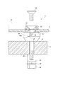
- the gap ball 6 is press-fitted and held in the inner wall surface of the second mounting hole 3B that penetrates the face plate 3. Specifically, the gap ball 6 is held only by the inner wall surface corresponding to the second mounting hole 3B in the aluminum substrate 31, and the holding position of the gap ball 6 in the second mounting hole 3B is aluminum.
- the gap ball 6 having a diameter larger than the thickness of the aluminum substrate 31 is press-fitted into a position slightly higher than the center in the thickness direction. In addition, a predetermined protrusion amount of the gap ball 6 is ensured.
- the gap ball 6 is press-fitted from above into the second mounting hole 3B. At this time, the surface of the anodized layer 34 applied to the inner wall surface of the aluminum substrate 31 is thinly removed at the press-fitted portion, but remains. . If the gap ball 6 is pressed into the second mounting hole 3B deeply below the center in the thickness direction of the aluminum substrate 31, the alumite layer 34 will be exposed to all the portions below the press-fitting site by external force from above. It peels off from the inner wall surface and may be lost at once. In this case, the holding force on the lower side of the gap ball 6 is reduced, so that the gap ball 6 cannot be stably held and the gap C cannot be maintained. On the other hand, in the present embodiment, the gap ball 6 is held at a position higher than the center of the aluminum substrate 31 in the plate thickness direction so that the gap C can be maintained more reliably without being lost. Yes.
- the second mounting hole 3B so as to penetrate the aluminum substrate 31, there is no bottom portion formed as a part of the aluminum substrate 31 in the second mounting hole 3B.
- the gap ball 6 is not placed on such a bottom portion. Accordingly, it is possible to eliminate the thermal influence exerted on the gap ball 6 by such deformation at the thin bottom portion. Even if the second mounting hole 3B does not penetrate the aluminum substrate 31 and the bottom portion is present on the aluminum substrate 31, the gap ball 6 may not be in contact with the bottom portion. The influence of the thermal expansion and contraction of the bottom portion on the gap ball 6 can be reduced.
- a grounding structure using the grounding member 8 will be described based on FIGS. 1, 6, and 7. 1 and 6, a fourth through hole 2D penetrating the front and back is provided in the center of the base plate 2, and a female screw is formed in the fourth through hole 2D.
- a screw hole 2E is provided at a position spaced apart from the fourth mounting hole 2D of the base plate 2 by a predetermined dimension.
- a fourth mounting hole 3D penetrating the front and back is provided at a position corresponding to the fourth through hole 2D of the face plate 3.
- a holding bolt 81 is screwed into the fourth through hole 2D of the base plate 2 from above.
- the holding bolt 81 has a male screw portion 82 that is screwed into the fourth through hole 2 ⁇ / b> D, and a columnar head portion 83 that is integrally provided at the upper end of the male screw portion 82.
- a guide hole 81 ⁇ / b> A penetrating along the axial direction is provided in the center of the holding bolt 81.
- the portion of the guide hole 81A corresponding to the head 83 is wider in the radial direction than the portion corresponding to the male screw portion 82, and is a holding portion 81B having a hexagonal shape in plan view.
- a hexagonal nut 89 is fitted to the holding portion 81B so as to be slidable up and down.
- a long screw 84 inserted from above into the fourth mounting hole 3 ⁇ / b> D of the face plate 2 is screwed into the nut 89.
- the long screw 84 is provided at the lower end side and is inserted into the guide hole 81A of the holding bolt 81, the rod part 84A, the male screw part 84B integrally provided at the upper end of the rod part 84A and screwed into the nut 89, It has a head portion 84 ⁇ / b> C that is integrally provided at the upper end of the male screw portion 84 ⁇ / b> B and is locked by a spot facing portion in the fourth mounting hole 3 ⁇ / b> D of the face plate 3.
- Such a long screw 84 passes through one end side (upper end side) of the ground member 8 interposed between the lower surface of the face plate 3 and the nut 89.
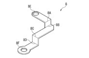
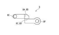
- the ground member 8 is a metal strip having conductivity such as stainless steel, and the first to fourth bent portions 8A, 8B, 8C, It is formed in a staircase shape having 8D.
- One end side of the ground member 8 is provided with an insertion hole 8E through which the long screw 84 is inserted, and the other end side (lower end side) is provided with an insertion hole 8F through which the screw 85 is inserted.
- the screw 85 is screwed into the screw hole 2E so that the other end side of the ground member 8 is sandwiched between the upper surface of the base plate 2 and the washer 86.
- a conductive metal washer 87 is disposed between the lower surface of the face plate 3 and the ground member 8, and is inserted through a long screw 84.
- the film heater 32A (FIGS. 2A and 2B) facing the washer 87 has an opening slightly larger than the diameter of the washer 87, and the aluminum substrate 31 (FIGS. 2A and 2B) also has the washer 87.
- Alumite treatment is not applied to the part slightly larger than the diameter.
- the thickness of the washer 87 is more than the thickness of the insulating layer which consists of the alumite layer 34 and the film heater 32A.
- the washer 87 is brought into contact with the base portion of the aluminum substrate 41 and becomes conductive, and the ground member 8 is connected to the aluminum substrate via the washer 87.
- the aluminum substrate 31 is grounded to the base plate 2 through the ground member 8.
- a resin washer 88 having heat insulation and insulation is disposed between the ground member 8 and the nut 89 and is inserted through the long screw 84. Therefore, it is difficult to transfer the heat from the face spray 3 to the nut 89 and the holding bolt 81, and heat transfer can be suppressed. Further, by providing the ground member 8 in the center, even if there is a heat escape, it is less affected from the viewpoint of uniformity than provided at the end.
- the first to fourth bent portions 8 A to 8 D are provided in the middle of the longitudinal direction, so that the external force acting on the ground member 8 is applied to the first to fourth bent portions 8 A. Absorbed by bending at ⁇ 8D, reaction force against external force hardly occurs at both ends of the ground member 8. Accordingly, the lower surface of the face plate 3 is not pressed upward particularly through the one end side of the ground member 8, and it is possible to prevent the center plate of the face plate 3 from being deformed so as to be pushed upward. Further, according to the ground member 8, the bending along the first to fourth bent portions 8A to 8D can cope with the displacement along the longitudinal direction due to the thermal expansion and contraction of the ground member 8.
- the other end side of the ground member 8 is fixed to the base plate 2 with the screws 85 in the previous step of supporting the face plate 3 on the base plate 2. Further, the nut 89 and the like are also accommodated in the holding portion 81B of the holding bolt 81 screwed into the base plate 2, and one end side of the ground member 8 is positioned above the nut 89 and the washers 87 and 88 are arranged. Keep it.
- the long screw 84 is inserted into the fourth mounting hole 3 ⁇ / b> D of the face plate 3, and at the same time, the ground member 8, the washers 87 and 88, the nut 89, and the holding bolt 81. Insert. Thereafter, when the rod portion 84A of the long screw 84 is rotated while being guided in the guide hole 81A of the holding bolt 81, the nut 89 is screwed into the long screw 84 and slides upward in the holding portion 81 without rotating. Finally, the ground member 8 and the washers 87 and 88 are sandwiched between the lower surface of the face plate 3 and the nut 89.
- the terminal block 9 includes an insulating resin base 91 fixed to the lower surface of the base plate 2, and a conductive pair of metal conductive plates 92 attached to the base 91. And a pressing member 93 attached to the outer end of the conduction plate 92.
- the outer edge of the base 91 is substantially flush with the end surface of the base plate 2.
- the base 91 is provided with two mounting grooves 91A along the inner and outer directions (same as the radial direction of the base plate 2), and the conduction plate 92 is disposed in the mounting groove 91A.
- a cylindrical member 94 made of resin having insulation properties is inserted into the through holes 91B and 92A.
- a screw 96 passed through a flat washer 95 and a spring washer 95 ′ is inserted into the cylindrical member 94, and the screw 96 is screwed into a screw hole 2 ⁇ / b> F provided in the base plate 2.
- the base 91 is fixed to the base plate 2, and the conduction plate 92 is attached to the base 91.
- the screw 96 screwed into the base plate 2 is insulated from the conductive plate 92 by being inserted into the cylindrical member 94, so that the conductive plate 92 is not electrically connected to the base plate 2.
- screw holes 92B are provided on both sides of the through hole 92A, and screws 97 are screwed into the screw holes 92B.
- the base 92 is provided with a round hole 91C at a position corresponding to the screw hole 92B.
- the round hole 91C is for avoiding interference between the tip of the screw 97 protruding from the screw hole 92B and the base 91. It is a hole.
- a screw 97 screwed inwardly of the conduction plate 92 is inserted into the crimp terminal 24A of the wiring 24 through a flat washer 98 and a spring washer 98 '.
- the wiring 24 is connected onto the conduction plate 92.
- a screw 97 screwed on the outer side of the conduction plate 92 is inserted into the holding member 93 via a flat washer 98 and a spring washer 98 ', and is also connected to the terminal 33 of the film heater 32A (FIGS. 2A and 2B). It is inserted.
- the terminal 33 is connected to the conduction plate 92 so as to be pressed by the pressing member 93.
- the base plate 2 and the terminal block 9 are shown as viewed from below. However, the operation of attaching the terminal block 9 to the base plate 2 and the operation of connecting the wiring 24 and the terminal 33 are performed on the base plate 2. This is done with the bottom side up.
- the terminal 33 connected to the terminal block 9 has a channel shape (a U shape) having first and second bent portions 33A and 33B in the middle of the longitudinal direction. Therefore, by having the first and second bent portions 33A and 33B, the external force acting on the terminal 33 is caused by the bending at the first and second bent portions 33A and 33B, similarly to the ground member 8 described above. Absorbed, the reaction force against the external force hardly occurs at both ends of the terminal 33. Therefore, the lower surface of the face plate 3 is not pressed upward or pulled downward, particularly via the terminal 33 base end side, and the outer periphery of the face plate 3 is pushed upward or pulled downward. Can be prevented from being deformed. Further, even if the face plate 3 is pushed up or pulled down for some reason, the terminals 33 are arranged at equal intervals, so that they are not deformed into irregular shapes and the influence of the deformation can be reduced. .
- the terminal block 9 is attached to the lower surface of the base plate 2, the work of connecting the terminals 33 can be facilitated by turning the lower surface of the base plate 2 upward, and the workability is good.
- the terminal block 9 is conventionally attached to the upper surface of the base plate 2 and accommodated in the space between the face plate 3, but by being attached to the lower surface of the base plate 2, the base play 2, the face plate 3, , And the overall thickness reduction of the heating device 1 can be promoted.
- the present invention is not limited to the above-described embodiments, and modifications, improvements, and the like within the scope that can achieve the object of the present invention are included in the present invention.
- the tension members 7 are provided in the vicinity of all the support portions by the support column 5, but the tension members 7 are not only in the vicinity of all the support portions but only in the vicinity of some appropriately selected support portions. Even when the member 7 is provided, it is included in the present invention, and the case where the tensile member 7 is provided in a place other than the vicinity of the support place in the support column 5 is also included in the present invention. In short, it is only necessary that the portion of the face plate 3 corresponding to the wafer W mounting region is urged downward by the tension member 7 from the base plate 2 side.
- the film heater 32A is used as the heating means according to the present invention, but it is not necessary to use the film heater as long as the circuit pattern for heat generation can be formed on the substrate itself.
- the coil spring 73 is used as the biasing means for the tension member 7, but it may be a columnar rubber member having elasticity.
- the shape of the earth member 8 is a linear form extended toward the radial direction outer side from the center of the heating apparatus 1 in planar view, it is not limited to such a shape.
- the extending direction of the second bent portion 8B may be changed by 90 degrees to form an L shape in plan view, as shown in FIGS. 10A and 10B.
- the extension direction may be changed again by 90 ° at the fourth bent portion 8D, and the crank shape may be formed in plan view.
- the first and second bent portions 8A and 8B are bent, and the third and fourth bent portions 8C and 8D are bent, so that they are orthogonal to each other. Can cope with displacement in direction.
- the present invention can be used for heating a semiconductor wafer.
- SYMBOLS 1 Heating device, 2 ... Base plate, 3 ... Face plate, 3B ... 2nd attachment hole which is an attachment hole, 5 ... Support
Landscapes
- Container, Conveyance, Adherence, Positioning, Of Wafer (AREA)
- Exposure Of Semiconductors, Excluding Electron Or Ion Beam Exposure (AREA)
Abstract
Description
また、特許文献2の別の実施例では、球体の径寸法を球体受穴の径寸法よりも大きくし、球体を球体受穴の周縁部分に当接させた状態にして、球体受穴内に充填した接合剤により球体を固定している。
また、特許文献2では、球体が底部分に直接接触していないが、硬化した接合剤を介して間接的に接触していることになり、やはり厚さの薄い底部分の熱膨張や収縮に影響され、同様な問題が生じる。
第3発明に係る加熱装置では、前記取付孔の内壁面にはアルマイト処理が施され、前記球体は前記アルミ基板の板厚方向の中央よりも上方側の位置まで圧入さていることを特徴とする。
以下、本発明の一実施形態を図面に基づいて説明する。
図1において、加熱装置1は、半導体製造工程に用いられるコータデベロッパ装置に搭載される装置であり、2点鎖線で示したシリコンウェハ等の半導体ウェハ(以下、単にウェハと称する)Wを、パターン焼付工程等の種々の工程に応じた所定温度に加熱するように構成されている。
また、ウェハWへ施す加工条件(レシピ)が変更となり、フェイスプレート3の温度を例えば高温から低温へ変更する場合には、冷却パイプ11に冷媒ガスが供給され、冷却パイプ11の噴出小孔(図示略)から噴出する冷媒ガスによってフェイスプレート3が冷却される。冷媒ガスはその後、遮断整流プレート12に案内されて、ベースプレート2の中央から排気される。フェイスプレート3が設定温度以下になると、冷媒ガスの供給が停止され、再びフェイスプレート3が加工条件に応じた設定温度に加熱保持される。
ベースプレート2は金属製であり、本実施形態ではステンレスが採用されている。このようなベースプレート2には、軽量化のための複数の開口部21や、フェイスプレート3を冷却するために用いた冷媒ガスを中央から排出する排気開口22が設けられている。ベースプレート2が十分な板厚寸法を有することで、加熱装置1全体の剛性を保証している。また、ベースプレート2の外周側の下面には、8つのターミナルブロック9が等周間隔で設けられ、外部から給電されている(図1に破線にて4つを図示)。
フェイスプレート3は、図2Aに示すように、アルミ基板31の上下両面にフィルムヒータ32(32A,32B)をホットプレスにより貼り付けた構造である。このようなフェイスプレート3は、図1に示すように、最も外周側に等周間隔で配置された8箇所のウェハガイド4、およびその内側の適宜な位置に複数配置された支柱5を介してベースプレート2に支持されている。ウェハガイド4および支柱5による具体的な支持構造についても、後述する。
さらに、図2Bに示すように、ダミーのフィルムヒータ32Bを設ける代わりに、線膨張係数差をなくす程度の厚さを有したアルマイト層34′をアルミ基板31の上面に形成してもよい。また、この場合には、アルミ基板31の下面には、アルマイト層を施さなくともよい。
その他、ベースプレート2とフェイスプレート3との間には、環状の冷却パイプ11および遮熱整流プレート12が配置されている。冷却パイプ11には、中央の排気開口22を通して供給パイプ13が接続され、供給パイプ13から冷却パイプ11内に冷媒ガスが供給される。冷媒ガスは、冷却パイプ11に設けられた複数の噴出小孔(図示略)から中央に向けて噴出し、フェイスプレート3を下側から冷却する。
遮熱整流プレート12は、冷却パイプ11から噴出した冷媒ガスをベースプレート2に設けられた開口部21より流出するのを防ぎ、中央の排気開口22に案内し、排気を促進するとともに、発熱中のフェイスプレート3からベースプレート2への輻射熱を遮断する。これにより、ベースプレート2の熱膨張や、ベースプレート2に取り付けられた各種部品への熱影響を抑制できる。
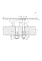
以下には、図1、図3を参照し、フェイスプレート3の外周側でのウェハガイド4による支持構造について説明する。
先ず、ベースプレート2の外周側の8箇所には、アルマイト処理が施された上下に貫通する第1貫通孔2Aが設けられている。これに対してウェハガイド4は、第1貫通孔2Aに上方から挿通される支持ボルト41と、フェイスプレート3の上面に配置されてウェハWの外周縁が当接される樹脂製のガイド部材42とを備えている。
次に、図1、図4を参照し、フェイスプレート3の支柱5による支持構造について説明する。
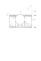
フェイスプレート3は、複数の支柱5を介してベースプレート2に支持されている。支柱5としては、2点鎖線で示したウェハWの外側にて等周間隔に配置された8本の支柱5Aと、その内側であるウェハWの載置領域にて等周間隔に配置された8本の支柱5Bと、さらにその内側にて等周間隔に配置された3本の支柱5Cとが設けられている。
支柱5による支持箇所近傍には、フェイスプレート3を下方に付勢する引張部材7が近接して設けられている。引張部材7は、支柱5による全ての支持箇所近傍に設けられる訳ではないが、支柱5としては、ギャップボール6および引張部材7が組み合わされて用いられている箇所では、必須である。支柱5は、単独での使用、または近傍にギャップボール6および引張部材7のいずれか一方が存在する箇所での使用が可能である。
図5に基づき、ギャップボール6の保持構造を説明する。
ギャップボール6は、フェイスプレート3を貫通する第2取付孔3Bの内壁面に圧入され、保持されている。詳細には、ギャップボール6は、アルミ基板31での第2取付孔3Bに対応した内壁面のみで保持されているのであり、その第2取付孔3Bでのギャップボール6の保持位置は、アルミ基板31の板厚方向の中央よりも上方側であって、本実施形態では、アルミ基板31の板厚寸法よりも大きい径寸法のギャップボール6を厚さ方向中央よりも僅かに高い位置に圧入し、ギャップボール6の所定の突出量を確保している。
図1、図6、図7に基づき、アース部材8による接地構造を説明する。
図1、図6において、ベースプレート2の中央には、表裏を貫通する第4貫通孔2Dが設けられ、第4貫通孔2D内には雌ねじが形成されている。また、ベースプレート2の第4取付孔2Dから所定寸法だけ離間した位置には、ねじ穴2Eが設けられている。
一方、フェイスプレート3の前記第4貫通孔2Dに対応した位置には、表裏を貫通する第4取付孔3Dが設けられている。
また、アース部材8によれば、第1~第4折曲部8A~8Dでの屈曲により、アース部材8の熱膨張や収縮による長手方向に沿った変位に対応できる。
図8において、ターミナルブロック9は、ベースプレート2の下面に固定される絶縁性を有した樹脂製の基台91と、基台91に取り付けられる導電性を有した一対の金属製の導通プレート92と、導通プレート92の外方側の端部に取り付けられる押さえ部材93とを備えている。
導通プレート92の外方側で螺入されるビス97は、平ワッシャ98およびスプリングワッシャ98′を介して押さえ部材93に挿通され、また、フィルムヒータ32A(図2A、図2B)の端子33に挿通される。ビス97をねじ穴92Bに螺入することで、端子33が押さえ部材93で押さえ込まれるようにして導通プレート92上に結線される。
なお、図8では、ベースプレート2やターミナルブロック9を下方から見た図として示されているが、ベースプレート2へのターミナルブロック9の取付作業や、配線24、端子33の結線作業は、ベースプレート2の下面を上方にして行われる。
しかも、ターミナルブロック9は従来、ベースプレート2の上面に取り付けられ、フェイスプレート3との間の空間に収容されていたが、ベースプレート2の下面に取り付けられることにより、ベースプレーと2とフェイスプレート3との間隔を全体的に狭めることができ、加熱装置1の全体的な薄型化を促進できる。
例えば、前記実施形態では、支柱5による全ての支持箇所近傍に対応して引張部材7が設けられていたが、全ての支持箇所近傍ではなく、適宜選択された幾つかの支持箇所近傍にのみ引張部材7を設けた場合でも本発明に含まれるし、支柱5での支持箇所近傍以外の箇所に引張部材7を設けた場合にも本発明に含まれる。要するに、フェイスプレート3のウェハW載置領域に対応した部分が、ベースプレート2側から引張部材7によって下方に付勢されていればよい。
前記実施形態では、引張部材7に係る付勢手段としてコイルばね73が用いられていたが、弾性力を有した円柱状のゴム部材等であってもよい。
これらの形状を有したアース部材8では、第1、第2折曲部8A,8Bが屈曲することと、第3、第4折曲部8C,8Dが屈曲することとにより、互いに直交する2方向の変位に対応できる。
Claims (4)
- ベースプレートと、
前記ベースプレートの上方に位置してウェハが載置されるフェイスプレートとを備え、
前記フェイスプレートは、
アルミ基板と、
前記アルミ基板に設けられて前記ウェハを加熱する加熱手段と、
前記アルミ基板に設けられて前記ウェハとの間に介装される球体とを備え、
前記アルミ基板には、前記球体が圧入される取付孔が設けられ、
前記球体は、前記圧入により前記取付孔内の内壁面でのみ保持されている
ことを特徴とする加熱装置。 - 請求項1に記載の加熱装置において、
前記取付孔は、前記アルミ基板を貫通して設けられている
ことを特徴とする加熱装置。 - 請求項1または請求項2に記載の加熱装置において、
前記取付孔の内壁面にはアルマイト処理が施され、
前記球体は前記アルミ基板の板厚方向の中央よりも上方側の位置まで圧入さている
ことを特徴とする加熱装置。 - ベースプレートと、
前記ベースプレートの上方に位置してウェハが載置されるフェイスプレートと、
前記ベースプレートおよび前記フェイスプレートの間に設けられて、前記フェイスプレートを冷却する冷媒ガスが流通する冷却パイプと、
前記ベースプレートおよび前記フェイスプレートの間に設けられて、前記冷却パイプを通して噴出された前記冷媒ガスを案内するとともに、前記フェイスプレートから前記ベースプレートへの輻射熱を遮熱する遮熱整流プレートと、
前記ベースプレートに取り付けられて、外部電源からの配線が結線されるターミナルブロックと、
前記ベースプレートおよび前記フェイスプレートの間に立設されて該フェイスプレートを支持する複数の支柱と、
前記フェイスプレートを前記ベースプレート側に引っ張る複数の引張部材とを備え、
前記フェイスプレートは、
アルミ基板と、
前記アルミ基板に設けられて前記ウェハを加熱するとともに、前記ターミナルブロックに接続される給電用の端子を有した加熱手段と、
前記アルミ基板に設けられて前記ウェハとの間に介装される球体とを備え、
前記アルミ基板には、前記球体が圧入される取付孔が設けられ、
前記球体は、前記圧入により前記取付孔内の内壁面でのみ保持されている
ことを特徴とする加熱装置。
Priority Applications (2)
| Application Number | Priority Date | Filing Date | Title |
|---|---|---|---|
| US14/008,287 US20140014643A1 (en) | 2011-03-28 | 2012-03-28 | Heating Device |
| KR1020137025583A KR101479052B1 (ko) | 2011-03-28 | 2012-03-28 | 가열 장치 |
Applications Claiming Priority (2)
| Application Number | Priority Date | Filing Date | Title |
|---|---|---|---|
| JP2011-071243 | 2011-03-28 | ||
| JP2011071243A JP5384549B2 (ja) | 2011-03-28 | 2011-03-28 | 加熱装置 |
Publications (1)
| Publication Number | Publication Date |
|---|---|
| WO2012133493A1 true WO2012133493A1 (ja) | 2012-10-04 |
Family
ID=46931202
Family Applications (1)
| Application Number | Title | Priority Date | Filing Date |
|---|---|---|---|
| PCT/JP2012/058073 Ceased WO2012133493A1 (ja) | 2011-03-28 | 2012-03-28 | 加熱装置 |
Country Status (4)
| Country | Link |
|---|---|
| US (1) | US20140014643A1 (ja) |
| JP (1) | JP5384549B2 (ja) |
| KR (1) | KR101479052B1 (ja) |
| WO (1) | WO2012133493A1 (ja) |
Cited By (1)
| Publication number | Priority date | Publication date | Assignee | Title |
|---|---|---|---|---|
| JP2012204827A (ja) * | 2011-03-28 | 2012-10-22 | Komatsu Ltd | 加熱装置 |
Families Citing this family (4)
| Publication number | Priority date | Publication date | Assignee | Title |
|---|---|---|---|---|
| JP5684023B2 (ja) * | 2011-03-28 | 2015-03-11 | 株式会社小松製作所 | 加熱装置 |
| JP6219227B2 (ja) | 2014-05-12 | 2017-10-25 | 東京エレクトロン株式会社 | ヒータ給電機構及びステージの温度制御方法 |
| JP6219229B2 (ja) * | 2014-05-19 | 2017-10-25 | 東京エレクトロン株式会社 | ヒータ給電機構 |
| KR102923085B1 (ko) * | 2022-03-29 | 2026-02-06 | 교세라 가부시키가이샤 | 시료 유지구 |
Citations (5)
| Publication number | Priority date | Publication date | Assignee | Title |
|---|---|---|---|---|
| JP2001508599A (ja) * | 1997-01-23 | 2001-06-26 | エーエスエム アメリカ インコーポレイテッド | ウェハ支持システム |
| JP2004200667A (ja) * | 2002-12-05 | 2004-07-15 | Ibiden Co Ltd | 金属ヒータ |
| JP2005064297A (ja) * | 2003-08-15 | 2005-03-10 | Dainippon Screen Mfg Co Ltd | 基板処理装置および基板処理方法 |
| JP2009146793A (ja) * | 2007-12-17 | 2009-07-02 | Nhk Spring Co Ltd | ヒータユニットとその製造方法 |
| JP2010129709A (ja) * | 2008-11-27 | 2010-06-10 | Kyocera Corp | 試料支持具および加熱装置 |
Family Cites Families (7)
| Publication number | Priority date | Publication date | Assignee | Title |
|---|---|---|---|---|
| JP2001237053A (ja) * | 1999-12-14 | 2001-08-31 | Ibiden Co Ltd | 半導体製造・検査装置用セラミックヒータおよび支持ピン |
| WO2004019658A1 (ja) * | 2002-08-20 | 2004-03-04 | Ibiden Co., Ltd. | 金属ヒータ |
| DE10258570B4 (de) * | 2002-12-14 | 2005-11-03 | Semikron Elektronik Gmbh & Co. Kg | Leistungshalbleitermodul |
| KR100505035B1 (ko) * | 2003-11-17 | 2005-07-29 | 삼성전자주식회사 | 기판을 지지하기 위한 정전척 |
| US20060289447A1 (en) * | 2005-06-20 | 2006-12-28 | Mohamed Zakaria A | Heating chuck assembly |
| JP4629574B2 (ja) * | 2005-12-27 | 2011-02-09 | 日本発條株式会社 | 基板支持装置と、その製造方法 |
| JP2010205922A (ja) * | 2009-03-03 | 2010-09-16 | Canon Anelva Corp | 基板熱処理装置及び基板の製造方法 |
-
2011
- 2011-03-28 JP JP2011071243A patent/JP5384549B2/ja not_active Expired - Fee Related
-
2012
- 2012-03-28 KR KR1020137025583A patent/KR101479052B1/ko not_active Expired - Fee Related
- 2012-03-28 WO PCT/JP2012/058073 patent/WO2012133493A1/ja not_active Ceased
- 2012-03-28 US US14/008,287 patent/US20140014643A1/en not_active Abandoned
Patent Citations (5)
| Publication number | Priority date | Publication date | Assignee | Title |
|---|---|---|---|---|
| JP2001508599A (ja) * | 1997-01-23 | 2001-06-26 | エーエスエム アメリカ インコーポレイテッド | ウェハ支持システム |
| JP2004200667A (ja) * | 2002-12-05 | 2004-07-15 | Ibiden Co Ltd | 金属ヒータ |
| JP2005064297A (ja) * | 2003-08-15 | 2005-03-10 | Dainippon Screen Mfg Co Ltd | 基板処理装置および基板処理方法 |
| JP2009146793A (ja) * | 2007-12-17 | 2009-07-02 | Nhk Spring Co Ltd | ヒータユニットとその製造方法 |
| JP2010129709A (ja) * | 2008-11-27 | 2010-06-10 | Kyocera Corp | 試料支持具および加熱装置 |
Cited By (1)
| Publication number | Priority date | Publication date | Assignee | Title |
|---|---|---|---|---|
| JP2012204827A (ja) * | 2011-03-28 | 2012-10-22 | Komatsu Ltd | 加熱装置 |
Also Published As
| Publication number | Publication date |
|---|---|
| KR101479052B1 (ko) | 2015-01-05 |
| JP5384549B2 (ja) | 2014-01-08 |
| KR20130129302A (ko) | 2013-11-27 |
| US20140014643A1 (en) | 2014-01-16 |
| JP2012204825A (ja) | 2012-10-22 |
Similar Documents
| Publication | Publication Date | Title |
|---|---|---|
| JP5203482B2 (ja) | 加熱装置 | |
| KR102322400B1 (ko) | 고온 전극 연결들 | |
| JP5384549B2 (ja) | 加熱装置 | |
| JP5694824B2 (ja) | 加熱装置 | |
| JP5684023B2 (ja) | 加熱装置 | |
| JP6341457B1 (ja) | 静電チャック | |
| JP6555922B2 (ja) | 加熱装置 | |
| US10978323B2 (en) | Substrate holder having integrated temperature measurement electrical devices | |
| JP6930826B2 (ja) | 熱閉塞体を備える静電チャック | |
| KR19980063620A (ko) | 반도체 웨이퍼 공정 처리 시스템내의 받침대에 웨이퍼를기계적 및 정전기적으로 크램핑하는 방법 및 장치 | |
| JP6958644B2 (ja) | 評価治具及び評価方法 | |
| JPWO2019142812A1 (ja) | ヒータベース及び処理装置 | |
| JP2013516776A (ja) | ヒートシンクで使用する熱プラグ及びその組立方法 | |
| US20220059375A1 (en) | System and method for heating semiconductor wafers | |
| JP6401638B2 (ja) | 加熱装置 | |
| JP5338720B2 (ja) | 加熱ヒータおよびそれを搭載した装置 | |
| JP2007165149A (ja) | Lgaコネクタ、パッケージ実装構造 | |
| JP2009053082A (ja) | 半導体試験装置及び半導体試験方法 | |
| JP2016189428A (ja) | 静電チャック装置 | |
| CN112928007A (zh) | 等离子体处理设备及用于等离子体处理设备的下电极组件 | |
| KR100816526B1 (ko) | 헬륨 공급부를 포함하는 정전척 장치 | |
| JP2019525479A (ja) | 接地クランプユニット及びこれを含む基板支持アセンブリー | |
| KR100812216B1 (ko) | 웨이퍼 고정용 정전척의 히터전원 로드 연결 장치 | |
| JPH10632A (ja) | 注型絶縁物の矯正治具 | |
| JP2011003731A (ja) | プラズマ処理装置用電極板 |
Legal Events
| Date | Code | Title | Description |
|---|---|---|---|
| 121 | Ep: the epo has been informed by wipo that ep was designated in this application |
Ref document number: 12764096 Country of ref document: EP Kind code of ref document: A1 |
|
| ENP | Entry into the national phase |
Ref document number: 20137025583 Country of ref document: KR Kind code of ref document: A |
|
| WWE | Wipo information: entry into national phase |
Ref document number: 14008287 Country of ref document: US |
|
| NENP | Non-entry into the national phase |
Ref country code: DE |
|
| 122 | Ep: pct application non-entry in european phase |
Ref document number: 12764096 Country of ref document: EP Kind code of ref document: A1 |