WO2012133401A1 - プラズマエッチングガス及びプラズマエッチング方法 - Google Patents
プラズマエッチングガス及びプラズマエッチング方法 Download PDFInfo
- Publication number
- WO2012133401A1 WO2012133401A1 PCT/JP2012/057921 JP2012057921W WO2012133401A1 WO 2012133401 A1 WO2012133401 A1 WO 2012133401A1 JP 2012057921 W JP2012057921 W JP 2012057921W WO 2012133401 A1 WO2012133401 A1 WO 2012133401A1
- Authority
- WO
- WIPO (PCT)
- Prior art keywords
- etching
- gas
- silicon
- film
- fluoro
- Prior art date
- Legal status (The legal status is an assumption and is not a legal conclusion. Google has not performed a legal analysis and makes no representation as to the accuracy of the status listed.)
- Ceased
Links
Classifications
-
- C—CHEMISTRY; METALLURGY
- C09—DYES; PAINTS; POLISHES; NATURAL RESINS; ADHESIVES; COMPOSITIONS NOT OTHERWISE PROVIDED FOR; APPLICATIONS OF MATERIALS NOT OTHERWISE PROVIDED FOR
- C09K—MATERIALS FOR MISCELLANEOUS APPLICATIONS, NOT PROVIDED FOR ELSEWHERE
- C09K13/00—Etching, surface-brightening or pickling compositions
-
- C—CHEMISTRY; METALLURGY
- C07—ORGANIC CHEMISTRY
- C07C—ACYCLIC OR CARBOCYCLIC COMPOUNDS
- C07C21/00—Acyclic unsaturated compounds containing halogen atoms
- C07C21/02—Acyclic unsaturated compounds containing halogen atoms containing carbon-to-carbon double bonds
- C07C21/18—Acyclic unsaturated compounds containing halogen atoms containing carbon-to-carbon double bonds containing fluorine
-
- C—CHEMISTRY; METALLURGY
- C09—DYES; PAINTS; POLISHES; NATURAL RESINS; ADHESIVES; COMPOSITIONS NOT OTHERWISE PROVIDED FOR; APPLICATIONS OF MATERIALS NOT OTHERWISE PROVIDED FOR
- C09K—MATERIALS FOR MISCELLANEOUS APPLICATIONS, NOT PROVIDED FOR ELSEWHERE
- C09K13/00—Etching, surface-brightening or pickling compositions
- C09K13/04—Etching, surface-brightening or pickling compositions containing an inorganic acid
- C09K13/08—Etching, surface-brightening or pickling compositions containing an inorganic acid containing a fluorine compound
-
- H—ELECTRICITY
- H10—SEMICONDUCTOR DEVICES; ELECTRIC SOLID-STATE DEVICES NOT OTHERWISE PROVIDED FOR
- H10P—GENERIC PROCESSES OR APPARATUS FOR THE MANUFACTURE OR TREATMENT OF DEVICES COVERED BY CLASS H10
- H10P50/00—Etching of wafers, substrates or parts of devices
- H10P50/20—Dry etching; Plasma etching; Reactive-ion etching
- H10P50/24—Dry etching; Plasma etching; Reactive-ion etching of semiconductor materials
- H10P50/242—Dry etching; Plasma etching; Reactive-ion etching of semiconductor materials of Group IV materials
-
- H—ELECTRICITY
- H10—SEMICONDUCTOR DEVICES; ELECTRIC SOLID-STATE DEVICES NOT OTHERWISE PROVIDED FOR
- H10P—GENERIC PROCESSES OR APPARATUS FOR THE MANUFACTURE OR TREATMENT OF DEVICES COVERED BY CLASS H10
- H10P50/00—Etching of wafers, substrates or parts of devices
- H10P50/20—Dry etching; Plasma etching; Reactive-ion etching
- H10P50/26—Dry etching; Plasma etching; Reactive-ion etching of conductive or resistive materials
- H10P50/264—Dry etching; Plasma etching; Reactive-ion etching of conductive or resistive materials by chemical means
- H10P50/266—Dry etching; Plasma etching; Reactive-ion etching of conductive or resistive materials by chemical means by vapour etching only
- H10P50/267—Dry etching; Plasma etching; Reactive-ion etching of conductive or resistive materials by chemical means by vapour etching only using plasmas
-
- H—ELECTRICITY
- H10—SEMICONDUCTOR DEVICES; ELECTRIC SOLID-STATE DEVICES NOT OTHERWISE PROVIDED FOR
- H10P—GENERIC PROCESSES OR APPARATUS FOR THE MANUFACTURE OR TREATMENT OF DEVICES COVERED BY CLASS H10
- H10P50/00—Etching of wafers, substrates or parts of devices
- H10P50/20—Dry etching; Plasma etching; Reactive-ion etching
- H10P50/26—Dry etching; Plasma etching; Reactive-ion etching of conductive or resistive materials
- H10P50/264—Dry etching; Plasma etching; Reactive-ion etching of conductive or resistive materials by chemical means
- H10P50/266—Dry etching; Plasma etching; Reactive-ion etching of conductive or resistive materials by chemical means by vapour etching only
- H10P50/267—Dry etching; Plasma etching; Reactive-ion etching of conductive or resistive materials by chemical means by vapour etching only using plasmas
- H10P50/268—Dry etching; Plasma etching; Reactive-ion etching of conductive or resistive materials by chemical means by vapour etching only using plasmas of silicon-containing layers
-
- H—ELECTRICITY
- H10—SEMICONDUCTOR DEVICES; ELECTRIC SOLID-STATE DEVICES NOT OTHERWISE PROVIDED FOR
- H10P—GENERIC PROCESSES OR APPARATUS FOR THE MANUFACTURE OR TREATMENT OF DEVICES COVERED BY CLASS H10
- H10P50/00—Etching of wafers, substrates or parts of devices
- H10P50/20—Dry etching; Plasma etching; Reactive-ion etching
- H10P50/28—Dry etching; Plasma etching; Reactive-ion etching of insulating materials
- H10P50/282—Dry etching; Plasma etching; Reactive-ion etching of insulating materials of inorganic materials
- H10P50/283—Dry etching; Plasma etching; Reactive-ion etching of insulating materials of inorganic materials by chemical means
Definitions
- the present invention relates to a plasma etching gas for selectively etching a silicon oxide film or a silicon nitride film with respect to the silicon oxide film or the silicon film when etching the silicon oxide film or the silicon nitride film covering the silicon film formed on the object to be processed. And a plasma etching method using the etching gas.
- C 3 H 5 F 3 gas which is one of the saturated fluorinated hydrocarbons proposed in Patent Document 1, will be an etching gas with a high selectivity (paragraph 0106). ). This is because a reaction product is deposited on the mask and a portion to be etched is etched.
- Patent Document 3 describes that C 3 H 7 F and C 3 H 6 F 2 function together with other etching gases such as C 4 F 6 gas and oxygen to function as a protective film forming material during etching. It is disclosed.
- Patent Document 4 discloses a contact hole having a high aspect ratio by selectively etching a silicon oxide film, a silicon nitride film, or the like with respect to a resist or silicon using a dry etching gas containing unsaturated perfluorocarbon. Can be formed (paragraph 0004).
- the present invention has been made in view of the above-described circumstances, and when etching a silicon oxide film or a silicon nitride film covering a silicon film formed on an object to be processed, the silicon oxide film or the silicon film is damaged. It is an object of the present invention to provide a plasma etching gas for selectively etching a silicon nitride film with respect to a silicon oxide film or a silicon film without giving the plasma, and a plasma etching method using this etching gas.
- an etching that does not use argon as a high-energy ion species in plasma is attracting attention from the viewpoint of not damaging other films, particularly the silicon film.
- the present inventors use 2,2-difluoro-n-butane specifically disclosed in Patent Document 1 as an etching gas, and in the absence of argon, the silicon nitride film is formed on the silicon oxide film and the silicon film. Selective etching was studied. However, it was found that the selectivity for both membranes was only about 4.
- etching gases (a) and (b) and the etching method (c).
- B The etching gas according to (a), further comprising oxygen gas and / or nitrogen gas.
- C A method of selectively etching a silicon nitride film with respect to a silicon oxide film or a silicon film using the etching gas according to claim 1 or 2.
- an etching gas containing an unsaturated fluorinated hydrocarbon represented by CxHyFz (x 3, 4 or 5 and y + z ⁇ 2x and y> z).
- the silicon nitride film can be selectively etched with respect to the silicon oxide film or the silicon film.
- etching refers to a technique of etching a very highly integrated fine pattern on a target object used in a manufacturing process of a semiconductor manufacturing apparatus, and more specifically, processing.
- a high frequency electric field is applied to the gas (unsaturated fluorinated hydrocarbon gas represented by the above formula) to cause glow discharge, and the gas compound is separated into chemically active ions, electrons, and radicals, and the chemical Etching using reaction.
- the “silicon oxide film” is a film made of silicon oxide formed by, for example, thermal oxidation of silicon or a CVD method using SiH 4 and O 2 as source gases.
- the “silicon film” is a film made substantially of Si, such as single crystal silicon, polycrystalline silicon, amorphous silicon or the like.
- the “silicon nitride film” is, for example, SiaNb (a, b> 0) formed by a low pressure CVD method using SiH 2 Cl 2 and NH 3 as source gases at a temperature condition of about 700 ° C. It is a film
- the unsaturated fluorinated hydrocarbon A may have a linear structure, a branched structure, or a cyclic structure.
- unsaturated fluorinated hydrocarbon A examples include the following. (Unsaturated fluorinated hydrocarbon represented by the formula: C 3 H 5 F) 3-fluoropropene, 2-fluoro-1-propene, (Z) -1-fluoro-1-propene, (E) -1- Fluoro-1-propene (formula: unsaturated fluorinated hydrocarbon represented by C 3 H 4 F 2 ) 3,3-difluoro-1-propene, 1,1-difluoro-1-propene, 1,2-difluoro -1-propene (unsaturated fluorinated hydrocarbon represented by the formula: C 3 H 3 F) propargyl fluoride, fluoroallene, 3-fluoro-1-cyclopropene, 1-fluoro-1-cyclopropene, 1- Fluoro-1-propyne (formula: unsaturated fluorinated hydrocarbon represented by C 4 H 7 F) 2-methyl-3-fluoro-1-propen
- unsaturated fluorinated hydrocarbons A are known substances, and can be produced and obtained by a conventionally known method. For example, it can be produced and obtained by the method described in Journal of American Chemical Society, 78, 2608 (1956). Further, a commercially available product can be used as it is or after purification as desired.
- the unsaturated fluorinated hydrocarbon A is filled in an arbitrary vessel, for example, a vessel such as a cylinder like the conventional semiconductor gas, and used for plasma etching described later.
- the purity of the unsaturated fluorinated hydrocarbon A (gas) is preferably 99% by volume or more, more preferably 99.9% by volume or more, and particularly preferably 99.98% by volume or more. When the purity is in the above range, the effect of the present invention is further improved. If the purity of the unsaturated fluorinated hydrocarbon A (gas) is too low, there may be a deviation in gas purity (content of unsaturated fluorinated hydrocarbon) in the container filled with gas. Specifically, the gas purity may be greatly different between the initial use stage and the stage where the remaining amount is low.
- the mixed gas is dissociated in the plasma reaction apparatus to generate various free radicals (etching species), which greatly affects the plasma reaction of the unsaturated fluorinated hydrocarbon A.
- impurities such as nitrogen gas, oxygen gas, and moisture
- the time when the container is opened and the unsaturated fluorinated hydrocarbon A in the container The difference in composition between the fluorinated unsaturated hydrocarbon gas coming out of the container and the impurity occurs at the time when the remaining amount of gas decreases, and the same etching performance cannot be obtained.
- the amount of nitrogen gas and oxygen gas contained as unsaturated trace gas in unsaturated fluorinated hydrocarbon A is 200 ppm by volume with respect to the total amount of fluorinated hydrocarbon (1) gas as the total amount of both. Or less, more preferably 150 ppm by volume or less, and particularly preferably 100 ppm by volume or less.
- the water content is preferably 30 ppm by weight or less, more preferably 20 ppm by weight or less, and particularly preferably 10 ppm by weight or less.
- the total amount of nitrogen gas and oxygen gas is the total content (ppm) of nitrogen gas and oxygen gas based on volume measured by gas chromatography analysis using the absolute calibration curve method.
- these volume standards can also be referred to as molar standards.
- the “water content” is usually a water content (ppm) based on weight measured by the Karl Fischer method.
- the etching gas preferably contains oxygen gas and / or nitrogen gas in addition to the unsaturated fluorinated hydrocarbon A gas.
- oxygen gas and / or nitrogen gas in combination, it is possible to dramatically increase the selectivity while preventing the stop of etching (etching stop), which is considered to be caused by the deposition of reactants on the bottom surface of the hole.
- the use ratio of oxygen gas and nitrogen gas is preferably 0.1 to 150 in terms of the total volume ratio of oxygen gas, nitrogen gas, or oxygen gas and nitrogen gas to unsaturated fluorinated hydrocarbon A gas, More preferably, it is 1-15.
- the introduction rate of the processing gas is proportional to the proportion of each component used.
- the unsaturated fluorinated hydrocarbon gas has a rate of 8.45 ⁇ 10 ⁇ 3 to 1.69 ⁇ 10 ⁇ 1 Pa ⁇ m 3 / sec (5 to 100 sccm) and oxygen gas may be 8.45 ⁇ 10 ⁇ 3 to 8.45 ⁇ 10 ⁇ 1 Pa ⁇ m 3 / sec (5 to 1500 sccm).
- the pressure in the processing chamber into which the etching gas is introduced is usually 0.1 to 100 Pa, preferably 1 to 10 Pa.
- a plasma generator generates plasma by generating a glow discharge by applying a high-frequency electric field to the unsaturated fluorinated hydrocarbon A gas (reactive plasma gas) in the processing chamber.
- plasma generators examples include helicon wave system, high frequency induction system, parallel plate type, magnetron system and microwave system. However, since plasma generation in a high density region is easy, helicon wave system, high frequency induction. The apparatus of a system and a microwave system is used suitably.
- the plasma density is not particularly limited. From the viewpoint of better expressing the effects of the present invention, etching is performed in a high-density plasma atmosphere with a plasma density of preferably 10 11 ions / cm 3 or more, more preferably 10 12 to 10 13 ions / cm 3 . Is desirable.
- the ultimate temperature of the substrate to be processed at the time of etching is not particularly limited, but is preferably in the range of ⁇ 50 to + 300 ° C., more preferably ⁇ 20 to + 100 ° C., and further preferably 0 to 50 ° C.
- the temperature of the substrate may or may not be controlled by cooling or the like.
- the plasma etching method of the present invention is a method for generating a plasma of an etching gas in a processing chamber and etching a predetermined portion on an object to be processed disposed therein, and comprising unsaturated fluorinated carbonization.
- an etching gas containing hydrogen it is preferable that the silicon nitride film be selectively plasma-etched, and the silicon nitride film and / or the silicon film is selectively plasma-etched with respect to the silicon oxide film and / or the silicon film. More preferably, it is a method.
- the selection ratio of the silicon nitride film to the silicon oxide film and / or the silicon film is at least 10 or more, and in many cases an infinite selection ratio It is possible to obtain a significantly higher selection ratio than the conventional one while avoiding the stop of etching due to the deposit.
- a wafer (2) on which a film (SiO 2 ; SiO in the table) is formed and a wafer (3) on which a polycrystalline silicon film (poly-Si; Si in the table) is formed are set.
- oxygen gas was introduced into the etching chamber at a rate of 2.03 ⁇ 10 ⁇ 1 Pa ⁇ m 3 / sec (120 sccm), and the non-conductivity obtained in Production Examples 1 to 3 was obtained.
- Each of the saturated fluorinated hydrocarbon gases was introduced at a flow rate of 1.69 ⁇ 10 ⁇ 2 to 1.69 ⁇ 10 ⁇ 1 Pa ⁇ m 3 / sec (10 to 100 sccm).
- the pressure in the system was maintained at 6.7 Pa, 200 W (60 MHz) was applied to the upper electrode, and 100 W (2 MHz) was applied to the lower electrode to perform plasma etching.
- the etching rates of the silicon nitride film of the wafer (1), the silicon oxide film of the wafer (2), and the silicon film of the wafer (3) are measured, and the silicon oxide film and silicon film are measured based on these measurement results.
- the selectivity was obtained from the ratio of the etching rates of the silicon nitride film.
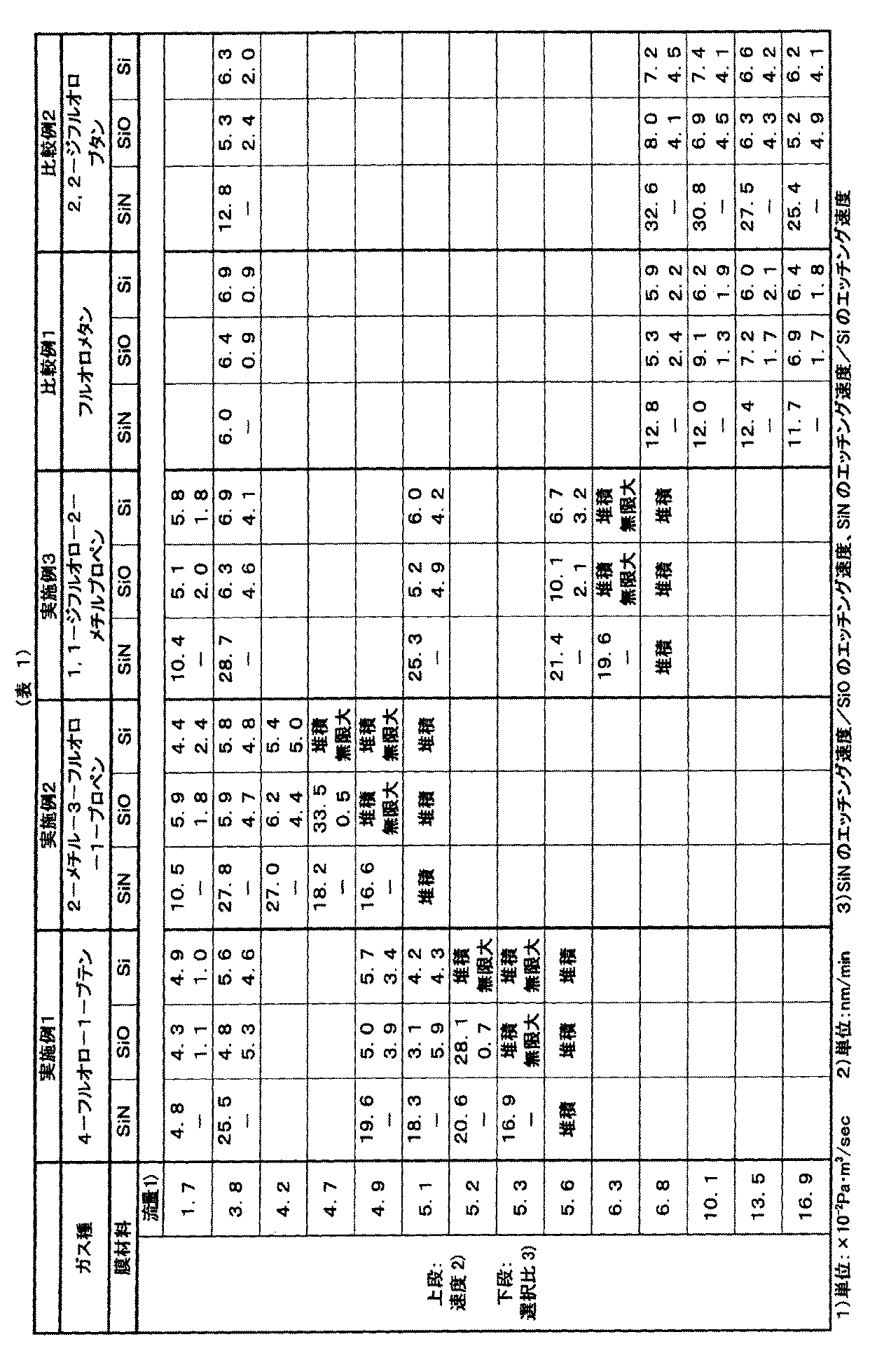
- Table 1 shows the etching rate measurement results and the selectivity calculation results for the silicon nitride film, silicon oxide film, and silicon film according to the flow rate of the etching gas of the present invention. The case where the etching did not proceed and the fluorocarbon film derived from the etching gas was deposited was indicated as “deposition” in the table.
Landscapes
- Chemical & Material Sciences (AREA)
- Organic Chemistry (AREA)
- Engineering & Computer Science (AREA)
- Materials Engineering (AREA)
- Inorganic Chemistry (AREA)
- Drying Of Semiconductors (AREA)
- Physics & Mathematics (AREA)
- Plasma & Fusion (AREA)
Abstract
Description
例えば、特許文献1では、シリコン酸化膜を被うシリコン窒化膜をエッチングする際に、シリコン窒化膜を選択的にエッチングするガスとして、CxHyFz(式中、xは3、4又は5、y、zはそれぞれ独立して、正の整数を表し、かつ、y>zである)であらわされる飽和フッ素化炭化水素が提案されている。そして、この文献の実施例においては、2,2-ジフルオロ-n-ブタンが、シリコン酸化膜をエッチングすることなく、シリコン窒化膜のみを64nm/分の速度で選択的にエッチングする(選択比は無限大)ことが示されている。
また、特許文献2によると、特許文献1に提案される飽和フッ素化炭化水素の一つであるC3H5F3ガスは、高い選択比のエッチングガスとなろうと推定されている(段落0106)。これは、マスクに反応生成物が堆積し、エッチングされるべき部分がエッチングされることによる。
同様に特許文献3には、C3H7F及びC3H6F2が、C4F6ガスや酸素等の他のエッチングガスと共に用いてエッチング時の保護膜形成物質として機能することが開示されている。
また、特許文献4には、不飽和パーフルオロカーボンを含むドライエッチングガスを用いて、シリコン酸化膜やシリコン窒化膜等をレジストやシリコンに対して選択的にエッチングすることで、高アスペクト比のコンタクトホールを形成できることが記載されている(段落0004)。
しかしながら、近年における半導体製造技術の進展に伴い、他の膜、特にシリコン膜やシリコン酸化膜にダメ-ジを与えることなく、シリコン窒化膜をシリコン酸化膜やシリコン膜等に対してより選択的にエッチングする技術の開発が求められているのが現状である。
本発明者らは、特許文献1に具体的に開示された2,2-ジフルオロ-n-ブタンをエッチングガスとして用いて、アルゴン不存在下で、シリコン窒化膜の、シリコン酸化膜及びシリコン膜に対する選択的エッチングを検討した。しかしながら、両膜に対する選択比は4程度しか得られないことが分かった。
(a)CxHyFz(x=3、4又は5である。また、y+z≦2x、かつy>zである。)で表される不飽和フッ素化炭化水素を含有するエッチングガス。
(b)更に、酸素ガス及び/又は窒素ガスを含む(a)に記載のエッチングガス。
(c)シリコン酸化膜又はシリコン膜に対してシリコン窒化膜を、請求項1又は2記載のエッチングガスを用いて選択的にエッチングする方法。
本発明において、「シリコン酸化膜」とは、例えば、シリコンの熱酸化やSiH4及びO2を原料ガスとしたCVD法によって形成される、ケイ素の酸化物からなる膜である。
本発明において、「シリコン膜」とは、単結晶シリコン、多結晶シリコン、アモルファスシリコン等の、実質的にSiのみからなる膜である。
本発明において、「シリコン窒化膜」とは、例えば、SiH2Cl2及びNH3を原料ガスとした約700℃程度の温度条件での減圧CVD法によって形成される、SiaNb(a、b>0)で表されるケイ素の窒化物からなる膜である。
本発明のエッチングガスは、CxHyFz(x=3、4又は5である。また、y+z≦2x、かつy>zである。)で表される不飽和フッ素化炭化水素(以下、「不飽和フッ素化炭化水素A」ということがある。)を含む。
不飽和フッ素化炭化水素Aは、直鎖構造を有するものであっても、分岐構造を有するものであってもよく、環状構造を有するものであってもよい。
(式:C3H5Fで表される不飽和フッ素化炭化水素)3-フルオロプロペン、2-フルオロ-1-プロペン、(Z)-1-フルオロ-1-プロペン、(E)-1-フルオロ-1-プロペン
(式:C3H4F2で表される不飽和フッ素化炭化水素)3,3-ジフルオロ-1-プロペン、1,1-ジフルオロ-1-プロペン、1,2-ジフルオロ-1-プロペン
(式:C3H3Fで表される不飽和フッ素化炭化水素)プロパルギルフルオリド、フルオロアレン、3-フルオロ-1-シクロプロペン、1-フルオロ-1-シクロプロペン、1-フルオロ-1-プロピン
(式:C4H7Fで表される不飽和フッ素化炭化水素)2-メチル-3-フルオロ-1-プロペン、(E)-1-フルオロ-2-ブテン、3-フルオロ-1-ブテン、(E)-2-フルオロ-2-ブテン、(Z)-2-フルオロ-2-ブテン、シクロプロピルメチルフルオリド、4-フルオロ-1-ブテン
(式:C4H6F2で表される不飽和フッ素化炭化水素)1,4-ジフルオロ-2-ブテン、1,1-ジフルオロ-2-メチルプロペン、(Z)-1,2-ジフルオロ-2-ブテン、3,3-ジフルオロ-1-ブテン、2-メチル-3,3-ジフルオロ-1-プロペン
(式:C4H5F3で表される不飽和フッ素化炭化水素)3,3,3-トリフルオロ-2-メチル-1-プロペン、4,4,4-トリフルオロ-1-ブテン、1,1,1-トリフルオロ-2-ブテン
(式:C4H5Fで表される不飽和フッ素化炭化水素)2-フルオロ-1,3-ブタジエン、2-フルオロ-1-メチレンシクロプロパン、3-フルオロシクロブテン、3-フルオロ-1-ブチン、(E)-1-フルオロ-1,3-ブタジエン、(Z)-1-フルオロ-1,3-ブタジエン、4-フルオロ-1-ブチン、1-フルオロ-2-ブチン
(式:C4H4F2で表される不飽和フッ素化炭化水素)1,1-ジフルオロ-1,3-ブタジエン、2,3-ジフルオロ-1,3-ブタジエン、1,2-ジフルオロ-1-シクロブテン、3,3-ジフルオロシクロブテン、(ジフルオロメチレン)シクロプロパン、(1E,3E)-1,4-ジフルオロ-1,3-ブタジエン、(1E,3Z)-1,4-ジフルオロ-1,3-ブタジエン、(1Z,3Z)-1,4-ジフルオロ-1,3-ブタジエン、1-メチレン-2,2-ジフルオロシクロプロパン、3,4-ジフルオロシクロブテン
(式:C4H3Fで表される不飽和フッ素化炭化水素)1-フルオロシクロブタジエン、1-フルオロ-1,2,3-ブタントリエン
(式:C5H9Fで表される不飽和フッ素化炭化水素)5-フルオロ-1-ペンテン、(E)-4-フルオロ-2-ペンテン、(Z)-4-フルオロ-2-ペンテン、2-フルオロ-3-メチル-2-ブテン
(式:C5H8F2で表される不飽和フッ素化炭化水素)2-メチル-1,1-ジフルオロ-1-ブテン
(式:C5H7F3で表される不飽和フッ素化炭化水素)4,4,4-トリフルオロ-2-メチル-1-ブテン、4,4,4-トリフルオロ-2-メチル-2-ブテン、5,5,5-トリフルオロ-1-ペンテン、3-トリフルオロメチル-1-ブテン、1-メチル-1-(トリフルオロメチル)シクロプロパン
(式:C5H7Fで表される不飽和フッ素化炭化水素)5-フルオロ-1,3-ペンタジエン、2-フルオロメチル-1,3-ブタジエン、[フルオロメチレン]シクロブタン、1-フルオロ-1-シクロペンテン、(E)-4-フルオロ-1,3-ペンタジエン、(Z)-4-フルオロ-1,3-ペンタジエン、(E)-5-フルオロ-1,3-ペンタジエン、(Z)-3-フルオロ-1,3-ペンタジエン、5-フルオロ-2-ペンチン、1-フルオロ-1,3-ペンタジエン、3-フルオロ-3-メチル-1-ブチン、-フルオロ-3-メチル-1,3-ブタジエン、5-フルオロ-1-ペンチン、3-フルオロ-1-シクロペンテン
(式:C5H6F2で表される不飽和フッ素化炭化水素)3,4-ジフルオロシクロペンテン、3,5-ジフルオロシクロペンテン、1,1-ジフルオロ-2-メチル-3-メチレンシクロプロパン、1,1-ジフルオロ-2-エチリデンシクロプロパン、1-メチル-2-(ジフルオロメチレン)シクロプロパン、1,1-ジフルオロ-2-メチル-1,3-ブタジエン、1,1-ジフルオロ-3-メチル-1,3-ブタジエン、3,3-ジフルオロ-1,4-ペンタジエン、(Z)-2,4-ジフルオロ-1,3-ペンタジエン、1,1-ジフルオロ-2-ビニルシクロプロパン
(式:C5H5F3で表される不飽和フッ素化炭化水素)3-(トリフルオロメチル)シクロブテン、2-(トリフルオロメチル)-1,3-ブタジエン、1,1,3-トリフルオロ-2-メチル-1,3-ブタジエン、1,1,2-トリフルオロ-1,3-ペンタジエン、1,1,2-トリフルオロ-1,4-ペンタジエン、(E)-5,5,5-トリフルオロ-1,3-ペンタジエン、(Z)-5,5,5-トリフルオロ-1,3-ペンタジエン、(1Z,3E)-1,3,5-トリフルオロ-1,3-ペンタジエン、(1E,3E)-1,3,5-トリフルオロ-1,3-ペンタジエン
(式:C5H5Fで表される不飽和フッ素化炭化水素)5-フルオロ-1,3-シクロペンタジエン、5,5-ジフルオロ-1,3-シクロペンタジエン
(式:C5H3Fで表される不飽和フッ素化炭化水素)1-フルオロ-1,3-ペンタジイン
これらの中でも、エッチング性能、及び入手や取り扱いの容易さから、4-フルオロ-1-ブテン、2-メチル-3-フルオロ-1-プロペン、および1,1-ジフルオロ-2-メチルプロペンが好ましい。
例えば、Journal of American Chemical Society,78,2608(1956)に記載された方法により製造し、入手することができる。また、市販品をそのままで、あるいは所望により精製した後に用いることもできる。
不飽和フッ素化炭化水素A(ガス)の純度は、好ましくは99容量%以上、さらに好ましくは99.9容量%以上、特に好ましくは99.98容量%以上である。純度が上記範囲にあることにより、本発明の効果がより一層向上する。また、不飽和フッ素化炭化水素A(ガス)の純度が低すぎると、ガスを充填した容器内において、ガス純度(不飽和フッ素化炭化水素の含有量)の偏りを生じる場合がある。具体的には、使用初期段階と残量が少なくなった段階とでのガス純度が大きく異なることがある。
なお、不飽和フッ素化炭化水素Aの純度は、内部標準物質法によるガスクロマトグラフィー分析で測定した重量基準の百分率(%)から導かれる容量基準の純度である。
ところが、不飽和フッ素化炭化水素A中、不純物として、空気や生産設備内の窒素ガス等;製造時に用いる溶媒;吸湿性が高い塩、アルカリ等に由来する水分等;が微量成分として存在することがある。
容器に充填された不飽和フッ素化炭化水素A中に、窒素ガス、酸素ガス、水分等が混在していると、その量を考慮して混合ガスを調整する必要が生じる。混在するガスは、プラズマ反応装置内で解離して、各種の遊離基(エッチング種)を発生させるため、不飽和フッ素化炭化水素Aのプラズマ反応に大きく影響するからである。
また、不飽和フッ素化炭化水素ガスAを充填した容器内に、窒素ガス、酸素ガス、水分等の不純物が存在する場合、当該容器を開封した時点と、容器内の不飽和フッ素化炭化水素Aガスの残量が少なくなった時点とで、容器から出てくるフッ素化不飽和炭化水素ガスと不純物の組成に違いが生じ、同一のエッチング性能を得ることができなくなる。
エッチングガスが導入された処理室内の圧力は、通常0.1~100Pa、好ましくは1~10Paである。
1リットルの四つ口フラスコに、3-ブテン-1-オール(72g)、乾燥テトラヒドロフラン(400ml)、及び、メタンスルホニルクロリド(126g)を仕込み、窒素気流下に置いた。フラスコを氷水でよく冷却し、滴下漏斗からトリエチルアミン(111g)をゆっくりと時間をかけて滴下した。滴下終了後、30分ほど氷水冷却下に攪拌し、その後、室温に戻して4時間ほど攪拌を継続した。反応終了後、テトラヒドロフランを100ml添加し、反応で生成する塩(トリエチルアミン塩酸塩)をろ別した。ろ液からエバポレータを使用してテトラヒドロフランの大部分を留去した。 得られた残渣にジエチルエーテルを200ml添加して、5%塩酸、飽和重曹水、飽和食塩水で順次洗浄後、無水硫酸マグネシウムで乾燥し、硫酸マグネシウムをろ別した。ろ液からエバポレータを使用してジエチルエーテルを留去して、4-メタンスルホニルオキシ-1-ブテン(以下、「メシレート」という)を黄褐色オイルとして126g得た(収率84%)。
0℃冷媒を循環させたジムロート型コンデンサーを備えた500mlガラス製反応器に、t-ブチルアンモニウムフルオライド3水和物75.7g(0.24mol)、乾燥ジメチルスルホキシド120mlを入れ、t-ブチルアンモニウムフルオライド3水和物を溶解させた。この溶液にメタリルクロリド18.1g(0.2mol)を添加し、窒素雰囲気下で10時間攪拌した。反応混合物を蒸留することにより、目的とする2-メチル-3-フルオロプロペンを10.8g得た(収率73%)。得られた2-メチル-3-フルオロプロペンの純度は99.8%であった。
ジムロート型コンデンサー及び滴下ロートを備えた100mlの3つ口フラスコ(反応器)を用意し、ジムロート型コンデンサーの上部にはガラス配管を組み、枝管を介してドライアイス/エタノール浴に浸した梨型フラスコを取り付けた。また、枝管から窒素を導入し、ジムロート型コンデンサーには15℃の冷媒を循環させた。
前記反応器内にLiAlH4 4.36g(0.115mol)を入れ、乾燥テトラヒドロフラン50mlを添加し、全容を室温で攪拌した。そこへ、3-クロロ-3,3-ジフルオロ-2-メチルプロペン 12.36g(0.1mol)を、滴下漏斗を用いて1時間かけてゆっくりと滴下した。滴下終了後、反応器を60℃に加温し、同温度でさらに4時間反応を継続した後、ジムロート型コンデンサーに循環させている冷媒の温度を20℃に上げ、反応混合物を65℃で1時間さらに加熱攪拌した。
得られた反応混合物から蒸留により、目的とする1,1-ジフルオロ-2-メチルプロペンを6.35g得た(収率69%)。得られた1,1-ジフルオロ-2-メチルプロペンの純度は99.5%であった。
平行平板型プラズマエッチング装置のエッチングチャンバ-内に、表面にシリコン窒化膜(Si3N4;下記表1中では、「SiN」と表記)が形成されたウエハ(1)と、表面にシリコン酸化膜(SiO2;表中ではSiO)が形成されたウエハ(2)と、表面に多結晶シリコン膜(poly-Si;表中ではSi)が形成されたウエハ(3)をそれぞれセットし、系内を真空にした後、酸素ガスを2.03×10⁻¹Pa・m3/sec(120sccm)の速度でエッチングチャンバ-内に導入した中に、上記製造例1~3で得られた不飽和フッ素化炭化水素ガスのそれぞれを、1.69×10-2~1.69×10-1Pa・m3/sec(10~100sccm)の流量で導入した。系内の圧力を6.7Paに維持し、上部電極に200W(60MHz)、下部電極に100W(2MHz)を印加して、プラズマエッチングを行った。そして、ウエハ(1)のシリコン窒化膜、ウエハ(2)のシリコン酸化膜、及びウエハ(3)のシリコン膜それぞれのエッチング速度を測定し、これらの測定結果に基づいてシリコン酸化膜及びシリコン膜に対するシリコン窒化膜のエッチング速度の比から選択比を求めた。
本発明のエッチングガスの流量別の、シリコン窒化膜、シリコン酸化膜及びシリコン膜の、エッチング速度の測定結果、及び選択比の計算結果を表1に示す。尚、エッチングが進まず、エッチングガス由来のフルオロカーボン膜が堆積した場合を、表中では「堆積」と表示した。
Claims (3)
- CxHyFz(x=3、4又は5である。また、y+z≦2x、かつy>zである。)で表される不飽和フッ素化炭化水素を含有するエッチングガス。
- 更に、酸素ガス及び/又は窒素ガスを含む請求項1記載のエッチングガス。
- シリコン酸化膜又はシリコン膜に対してシリコン窒化膜を、請求項1又は2記載のエッチングガスを用いて選択的にエッチングする方法。
Priority Applications (3)
| Application Number | Priority Date | Filing Date | Title |
|---|---|---|---|
| JP2013507609A JP5942985B2 (ja) | 2011-03-29 | 2012-03-27 | プラズマエッチングガス及びプラズマエッチング方法 |
| KR1020137025589A KR101962191B1 (ko) | 2011-03-29 | 2012-03-27 | 플라즈마 에칭 가스 및 플라즈마 에칭 방법 |
| US14/008,354 US9296947B2 (en) | 2011-03-29 | 2012-03-27 | Plasma etching gas and plasma etching method |
Applications Claiming Priority (2)
| Application Number | Priority Date | Filing Date | Title |
|---|---|---|---|
| JP2011072192 | 2011-03-29 | ||
| JP2011-072192 | 2011-03-29 |
Publications (1)
| Publication Number | Publication Date |
|---|---|
| WO2012133401A1 true WO2012133401A1 (ja) | 2012-10-04 |
Family
ID=46931117
Family Applications (1)
| Application Number | Title | Priority Date | Filing Date |
|---|---|---|---|
| PCT/JP2012/057921 Ceased WO2012133401A1 (ja) | 2011-03-29 | 2012-03-27 | プラズマエッチングガス及びプラズマエッチング方法 |
Country Status (5)
| Country | Link |
|---|---|
| US (1) | US9296947B2 (ja) |
| JP (1) | JP5942985B2 (ja) |
| KR (1) | KR101962191B1 (ja) |
| TW (1) | TWI559401B (ja) |
| WO (1) | WO2012133401A1 (ja) |
Cited By (1)
| Publication number | Priority date | Publication date | Assignee | Title |
|---|---|---|---|---|
| JP2014185111A (ja) * | 2013-03-25 | 2014-10-02 | Nippon Zeon Co Ltd | 高純度2,2−ジフルオロブタン |
Families Citing this family (6)
| Publication number | Priority date | Publication date | Assignee | Title |
|---|---|---|---|---|
| JP2016178222A (ja) * | 2015-03-20 | 2016-10-06 | ルネサスエレクトロニクス株式会社 | 半導体装置の製造方法 |
| JP6327295B2 (ja) * | 2015-08-12 | 2018-05-23 | セントラル硝子株式会社 | ドライエッチング方法 |
| JP6748354B2 (ja) | 2015-09-18 | 2020-09-02 | セントラル硝子株式会社 | ドライエッチング方法及びドライエッチング剤 |
| CN107731686A (zh) * | 2016-08-12 | 2018-02-23 | 中芯国际集成电路制造(上海)有限公司 | 半导体结构的形成方法 |
| US10629449B2 (en) | 2016-10-13 | 2020-04-21 | Kanto Denka Kogyo Co., Ltd. | Gas composition for dry etching and dry etching method |
| EP3608945A4 (en) | 2017-04-06 | 2020-12-23 | Kanto Denka Kogyo Co., Ltd. | COMPOSITION OF DRY ENGRAVING GAS AND DRY ENGRAVING PROCESS |
Citations (4)
| Publication number | Priority date | Publication date | Assignee | Title |
|---|---|---|---|---|
| JPS60115232A (ja) * | 1983-11-28 | 1985-06-21 | Hitachi Ltd | ドライエッチング用ガス |
| JPH04170026A (ja) * | 1990-11-02 | 1992-06-17 | Sony Corp | ドライエッチング方法 |
| WO2009123038A1 (ja) * | 2008-03-31 | 2009-10-08 | 日本ゼオン株式会社 | プラズマエッチング方法 |
| JP2011044740A (ja) * | 2000-04-28 | 2011-03-03 | Daikin Industries Ltd | ドライエッチングガスおよびドライエッチング方法 |
Family Cites Families (7)
| Publication number | Priority date | Publication date | Assignee | Title |
|---|---|---|---|---|
| DE3420347A1 (de) | 1983-06-01 | 1984-12-06 | Hitachi, Ltd., Tokio/Tokyo | Gas und verfahren zum selektiven aetzen von siliciumnitrid |
| JP2001250817A (ja) | 1999-12-28 | 2001-09-14 | Toshiba Corp | ドライエッチング方法及び半導体装置の製造方法 |
| TW486733B (en) | 1999-12-28 | 2002-05-11 | Toshiba Corp | Dry etching method and manufacturing method of semiconductor device for realizing high selective etching |
| JP4839506B2 (ja) | 2000-04-28 | 2011-12-21 | ダイキン工業株式会社 | ドライエッチング方法 |
| US7169695B2 (en) | 2002-10-11 | 2007-01-30 | Lam Research Corporation | Method for forming a dual damascene structure |
| JP2006310634A (ja) * | 2005-04-28 | 2006-11-09 | Sharp Corp | 半導体装置の製造方法 |
| US8765613B2 (en) * | 2011-10-26 | 2014-07-01 | International Business Machines Corporation | High selectivity nitride etch process |
-
2012
- 2012-03-27 JP JP2013507609A patent/JP5942985B2/ja not_active Expired - Fee Related
- 2012-03-27 US US14/008,354 patent/US9296947B2/en active Active
- 2012-03-27 WO PCT/JP2012/057921 patent/WO2012133401A1/ja not_active Ceased
- 2012-03-27 KR KR1020137025589A patent/KR101962191B1/ko not_active Expired - Fee Related
- 2012-03-28 TW TW101110683A patent/TWI559401B/zh not_active IP Right Cessation
Patent Citations (4)
| Publication number | Priority date | Publication date | Assignee | Title |
|---|---|---|---|---|
| JPS60115232A (ja) * | 1983-11-28 | 1985-06-21 | Hitachi Ltd | ドライエッチング用ガス |
| JPH04170026A (ja) * | 1990-11-02 | 1992-06-17 | Sony Corp | ドライエッチング方法 |
| JP2011044740A (ja) * | 2000-04-28 | 2011-03-03 | Daikin Industries Ltd | ドライエッチングガスおよびドライエッチング方法 |
| WO2009123038A1 (ja) * | 2008-03-31 | 2009-10-08 | 日本ゼオン株式会社 | プラズマエッチング方法 |
Cited By (1)
| Publication number | Priority date | Publication date | Assignee | Title |
|---|---|---|---|---|
| JP2014185111A (ja) * | 2013-03-25 | 2014-10-02 | Nippon Zeon Co Ltd | 高純度2,2−ジフルオロブタン |
Also Published As
| Publication number | Publication date |
|---|---|
| JP5942985B2 (ja) | 2016-06-29 |
| KR101962191B1 (ko) | 2019-03-26 |
| TW201250836A (en) | 2012-12-16 |
| TWI559401B (zh) | 2016-11-21 |
| KR20140016912A (ko) | 2014-02-10 |
| JPWO2012133401A1 (ja) | 2014-07-28 |
| US20140306146A1 (en) | 2014-10-16 |
| US9296947B2 (en) | 2016-03-29 |
Similar Documents
| Publication | Publication Date | Title |
|---|---|---|
| JP5440170B2 (ja) | プラズマエッチング方法 | |
| JP5942985B2 (ja) | プラズマエッチングガス及びプラズマエッチング方法 | |
| EP3214640B1 (en) | Plasma etching method | |
| US11566177B2 (en) | Dry etching agent, dry etching method and method for producing semiconductor device | |
| JP4978512B2 (ja) | プラズマエッチング方法 | |
| JP5131436B2 (ja) | エッチング方法 | |
| TWI653213B (zh) | High-purity 1-fluorobutane and plasma etching method | |
| JP2006156539A (ja) | プラズマ反応用ガス | |
| JPWO2015064550A1 (ja) | 高純度フッ素化炭化水素、プラズマエッチング用ガスとしての使用、及び、プラズマエッチング方法 | |
| TWI892472B (zh) | 使用含氧氫氟烴之蝕刻方法 | |
| KR100562514B1 (ko) | 세정 가스 및 식각 가스 | |
| TWI892471B (zh) | 使用含氧氫氟烴形成高縱橫比孔之蝕刻方法 | |
| JP3988496B2 (ja) | プラズマ反応性ガスおよびフッ素含有有機膜の形成方法 | |
| TW201906007A (zh) | 電漿處理裝置的陳化方法及電漿蝕刻方法 | |
| JP2010045058A (ja) | プラズマ反応用ガス |
Legal Events
| Date | Code | Title | Description |
|---|---|---|---|
| 121 | Ep: the epo has been informed by wipo that ep was designated in this application |
Ref document number: 12765622 Country of ref document: EP Kind code of ref document: A1 |
|
| ENP | Entry into the national phase |
Ref document number: 2013507609 Country of ref document: JP Kind code of ref document: A |
|
| ENP | Entry into the national phase |
Ref document number: 20137025589 Country of ref document: KR Kind code of ref document: A |
|
| NENP | Non-entry into the national phase |
Ref country code: DE |
|
| 122 | Ep: pct application non-entry in european phase |
Ref document number: 12765622 Country of ref document: EP Kind code of ref document: A1 |
|
| WWE | Wipo information: entry into national phase |
Ref document number: 14008354 Country of ref document: US |