WO2012132862A1 - 有機エレクトロルミネッセンスディスプレイとその製造方法 - Google Patents
有機エレクトロルミネッセンスディスプレイとその製造方法 Download PDFInfo
- Publication number
- WO2012132862A1 WO2012132862A1 PCT/JP2012/056311 JP2012056311W WO2012132862A1 WO 2012132862 A1 WO2012132862 A1 WO 2012132862A1 JP 2012056311 W JP2012056311 W JP 2012056311W WO 2012132862 A1 WO2012132862 A1 WO 2012132862A1
- Authority
- WO
- WIPO (PCT)
- Prior art keywords
- partition
- organic
- light emitting
- layer
- opening area
- Prior art date
- Legal status (The legal status is an assumption and is not a legal conclusion. Google has not performed a legal analysis and makes no representation as to the accuracy of the status listed.)
- Ceased
Links
Images




Classifications
-
- H—ELECTRICITY
- H05—ELECTRIC TECHNIQUES NOT OTHERWISE PROVIDED FOR
- H05B—ELECTRIC HEATING; ELECTRIC LIGHT SOURCES NOT OTHERWISE PROVIDED FOR; CIRCUIT ARRANGEMENTS FOR ELECTRIC LIGHT SOURCES, IN GENERAL
- H05B33/00—Electroluminescent light sources
- H05B33/02—Details
-
- H—ELECTRICITY
- H05—ELECTRIC TECHNIQUES NOT OTHERWISE PROVIDED FOR
- H05B—ELECTRIC HEATING; ELECTRIC LIGHT SOURCES NOT OTHERWISE PROVIDED FOR; CIRCUIT ARRANGEMENTS FOR ELECTRIC LIGHT SOURCES, IN GENERAL
- H05B33/00—Electroluminescent light sources
- H05B33/10—Apparatus or processes specially adapted to the manufacture of electroluminescent light sources
-
- H—ELECTRICITY
- H10—SEMICONDUCTOR DEVICES; ELECTRIC SOLID-STATE DEVICES NOT OTHERWISE PROVIDED FOR
- H10K—ORGANIC ELECTRIC SOLID-STATE DEVICES
- H10K59/00—Integrated devices, or assemblies of multiple devices, comprising at least one organic light-emitting element covered by group H10K50/00
- H10K59/10—OLED displays
- H10K59/12—Active-matrix OLED [AMOLED] displays
- H10K59/122—Pixel-defining structures or layers, e.g. banks
-
- H—ELECTRICITY
- H10—SEMICONDUCTOR DEVICES; ELECTRIC SOLID-STATE DEVICES NOT OTHERWISE PROVIDED FOR
- H10K—ORGANIC ELECTRIC SOLID-STATE DEVICES
- H10K59/00—Integrated devices, or assemblies of multiple devices, comprising at least one organic light-emitting element covered by group H10K50/00
- H10K59/30—Devices specially adapted for multicolour light emission
- H10K59/35—Devices specially adapted for multicolour light emission comprising red-green-blue [RGB] subpixels
- H10K59/352—Devices specially adapted for multicolour light emission comprising red-green-blue [RGB] subpixels the areas of the RGB subpixels being different
-
- H—ELECTRICITY
- H10—SEMICONDUCTOR DEVICES; ELECTRIC SOLID-STATE DEVICES NOT OTHERWISE PROVIDED FOR
- H10K—ORGANIC ELECTRIC SOLID-STATE DEVICES
- H10K2102/00—Constructional details relating to the organic devices covered by this subclass
- H10K2102/301—Details of OLEDs
- H10K2102/351—Thickness
Definitions
- the present invention relates to an organic electroluminescence display and a method for producing the same.
- An organic electroluminescence element (hereinafter referred to as an organic EL element) is an element in which an organic light emitting layer made of an organic light emitting material is formed between two opposing electrodes, and light is emitted by passing a current through the organic light emitting layer.
- the thickness of the organic light emitting layer is important for producing a good and reliable device.
- organic EL display in order to produce an organic electroluminescence display (hereinafter sometimes abbreviated as “organic EL display” as appropriate) using this, it is necessary to pattern the organic EL element itself with high definition.
- a patterned photosensitive polyimide resin or a photosensitive novolac resist formed in a partition shape so as to partition subpixels is used as a substrate for an organic EL display.
- the partition pattern is formed so as to cover the edge portion of the transparent electrode formed as an anode.
- a dry film formation method A derivative of polythiophene dispersed in is used.
- an inorganic material such as an organic material having a hole transporting capability or a metal oxide is formed using a vapor deposition method or a sputtering method.
- dry coating it is possible to coat the entire surface relatively easily and uniformly.
- a hole transport layer is formed between the hole injection layer and the light emitting layer.
- the formation method is the same as that of the hole injection layer.
- a dry film forming method which is a dry film forming method that facilitates uniform film formation
- a fine pattern mask is used. It is necessary to carry out patterning using, and it is very difficult to make a large substrate or fine patterning.
- the layer structure is a two-layer structure in which a hole transport layer and an organic light-emitting layer are laminated in order from the anode side Is common.
- the organic light-emitting layer is an organic light-emitting material in which organic light-emitting materials having respective emission colors of red (R), green (G), and blue (B) are dissolved or stably dispersed in a solvent to form a color panel.
- the ink can be applied separately (see Patent Document 1).
- a carrier injection layer (also called a carrier transport layer) is formed between the electrodes.
- the carrier injection layer controls the injection amount of electrons when injecting electrons from the electrode to the organic light emitting layer, or controls the injection amount of holes when holes are injected from the other electrode to the organic light emitting layer.
- a layer used to control and refers to a layer inserted between an electrode and an organic light emitting layer.
- the electron injection layer used to control the amount of electrons injected includes an electron-transporting organic substance such as a metal complex of a quinolinol derivative, or an alkali metal having a relatively low work function such as Ca or Ba. In some cases, a plurality of layers having these functions may be used.
- R, G, and B subpixels in one pixel have the same shape and the same area by the partition formed of photosensitive polyimide or photosensitive novolac resist as described above. It is divided like this.
- the luminance half-life times of R, G, and B are generally different, there is a problem that when the display is driven for a long time, the color balance changes and the color of the moving image changes.
- R, G, and B subpixels in one pixel are partitioned by a partition made of photosensitive polyimide, photosensitive novolac, or photosensitive acrylic material as described above.
- the light emitting areas of the subpixels that are normally partitioned are laid out in the same shape and the same area.
- the luminance half-times of R, G, and B are different, there is a problem that when the display is driven for a long time, the color balance changes and the emission color changes.
- the subpixel area is divided into partitions by partitions according to the luminance halving characteristics of R, G, and B, thereby improving color change and luminance half-life.
- the technique which takes this is taken (for example, refer patent document 1).
- 2A is a plan view
- FIG. 2B is an XY cross-sectional view of FIG. 2A.
- a main object of the present invention is to provide an organic electroluminescence display panel having good light emission characteristics and a method for manufacturing the same even if the areas of sub-pixels of each color are different.
- the present invention employs the following configuration in order to solve the above-described problems.
- the method for manufacturing an organic electroluminescence display panel includes a step of forming a first electrode for each pixel on a substrate and a first partition for partitioning the first electrode into at least two different opening areas.
- a partition formation step, a second partition formation step for forming a second partition partitioning the pixel with at least two different opening areas on the first partition, and a part of the light emitting medium layer are formed by a wet film formation method.
- the second partition is formed so as to be smaller than the area ratio of the opening area.
- the first partition may be formed so that the height of the first partition is 1 ⁇ m or less.
- the second partition may be formed so that the height of the second partition is 1 ⁇ m or more.
- the second partition may be formed so that the area ratio between the maximum opening area and the minimum opening area defined by the second partition is 2: 1 or less.
- the light emitting medium layer is an organic light emitting layer
- any one of a relief printing method, an ink jet method, and a nozzle printing method may be used as a wet film forming method.
- this invention is comprised as a manufacturing method of an organic electroluminescent display panel.
- the present invention may be configured as an organic electroluminescence display, an organic electroluminescence element, or the like.
- the organic electroluminescence display panel (organic EL display panel) is partitioned by the second partition so as to be smaller than the ratio of the opening area between the sub-pixels of different colors partitioned by the first partition.
- a substrate with partition walls is formed so that the opening areas between sub-pixels of different colors are aligned as much as possible.
- the opening area of the second partition is set to be approximately equal, so that the partition is defined by the second partition. Since the ink is uniformly applied to the light-emitting area and the ink is uniformly applied to the light-emitting areas having different areas, stable film formation with the same film thickness is possible, and the film formed on the partition is also uniform.
- the light emitting layer to be printed can be formed with a uniform film thickness and shape. As described above, according to the present invention, it is possible to provide a method of manufacturing an organic EL display panel having good light emission characteristics even when the subpixel areas of the respective colors are different.
- substrate with a partition used for the organic electroluminescent display which is one Embodiment of this invention Schematic showing a conventional substrate with a partition for an organic EL display
- Sectional drawing which shows the organic electroluminescent display which is one Embodiment of this invention
- FIGS. 1A and 1B are diagrams showing a substrate with a partition wall used in the organic EL display according to the present embodiment.
- FIG. 1A is a plan view
- FIG. 1B is an XY line in FIG.
- FIG. 5 is a cross-sectional view showing details of the cross-sectional view shown in FIG.
- the organic EL element of the present embodiment includes a first electrode 102 (hereinafter sometimes referred to as a pixel electrode 102) formed on a substrate 101 and a second electrode 107 (hereinafter referred to as a counter electrode) formed to face the first electrode 102.
- the light emitting medium layer 108 includes at least an organic light emitting layer that contributes to light emission, a carrier injection layer for injecting electrons or holes, and a carrier transport layer for transporting electrons or holes from the carrier injection layer to the light emitting layer. It is out.
- the light emitting medium layer 108 includes an electron injection layer and a hole blocking layer (electron transport layer) between the cathode and the light emitting layer, and a hole injection layer and electron blocking layer (hole transport layer) between the anode and the light emitting layer. It is formed by laminating as necessary.
- the organic EL element of this embodiment has a first partition wall 103 for partitioning an organic light emitting layer, and has a second partition wall 105 thereon.
- a full-color organic EL display panel can be manufactured by separately coating the light emitting layer constituting each pixel in, for example, three colors of R, G, and B.
- a light emitting material that emits white light so that the entire surface emits white light, or a laminated structure of layers that emit light of at least two colors is formed on the entire display region and is colored using a color filter.
- a full-color organic EL display panel can be produced.
- the configuration of the organic EL display of the present embodiment will be described in detail.
- an active matrix drive type organic EL display in which the first electrode 102 is an anode and the second electrode 107 is a cathode will be described (see FIG. 5).
- the first electrode 102 is formed as a pixel electrode partitioned by the first partition 103 for each pixel.
- the second partition wall 105 is installed in contact with the first partition wall 103.
- the first carrier injection layer formed on the first electrode 102 side is a hole transporting hole injection layer.
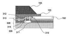
- FIG. 3 shows an example of a TFT substrate with a partition wall used in the organic EL display of this embodiment.
- a substrate (back plane) 308 used in the active matrix driving type organic EL display of the present embodiment is provided with a thin film transistor (TFT) and a lower electrode (pixel electrode 102) of the organic EL display device, and the TFT and The lower electrode is electrically connected.
- TFT thin film transistor
- pixel electrode 102 pixel electrode
- the TFT and the active matrix drive type organic EL display constructed above are supported by a support.
- Any material can be used as the support as long as it has mechanical strength and insulation and is excellent in dimensional stability.
- plastic films and sheets such as glass, quartz, polypropylene, polyethersulfone, polycarbonate, cycloolefin polymer, polyarylate, polyamide, polymethyl methacrylate, polyethylene terephthalate, polyethylene naphthalate, etc., or oxidation to these plastic films and sheets
- Metal oxides such as silicon and aluminum oxide, metal fluorides such as aluminum fluoride and magnesium fluoride, metal nitrides such as silicon nitride and aluminum nitride, metal oxynitrides such as silicon oxynitride, acrylic resins and epoxy resins
- Translucent base material with a single layer or laminated polymer resin film such as silicone resin or polyester resin, metal foil such as aluminum or stainless steel, sheet, plate, aluminum on the plastic film or sheet It can be
- the support made of these materials has been subjected to moisture-proofing treatment or hydrophobic treatment by forming an inorganic film or applying a fluororesin. It is preferable. In particular, in order to avoid moisture intrusion into the light emitting medium layer 108, it is preferable to reduce the moisture content and gas permeability coefficient of the support.
- a known thin film transistor can be used as the thin film transistor provided on the support. Specifically, as illustrated in FIG. 3, a thin film transistor mainly including an active layer 311 in which source / drain regions and a channel region are formed, a gate insulating film 309, and a gate electrode 314 can be given.
- the structure of the thin film transistor is not particularly limited, and examples thereof include a staggered type, an inverted staggered type, a top gate type, and a coplanar type.
- the active layer 311 is not particularly limited, and examples thereof include inorganic semiconductor materials such as amorphous silicon, polycrystalline silicon, microcrystalline silicon, cadmium selenide, thiophene oligomers, poly (p-ferylene vinylene), and the like.
- the organic semiconductor material can be used.
- These active layers 311 can be formed by, for example, laminating amorphous silicon by plasma CVD and ion doping; forming amorphous silicon by LPCVD using SiH4 gas, and amorphous silicon by solid phase growth.
- ion doping is performed by ion implantation; amorphous silicon is formed by LPCVD using Si 2 H 6 gas and PECVD using SiH 4 gas, and laser such as excimer laser After annealing, the amorphous silicon is crystallized to obtain polysilicon, then ion doping is performed by ion doping (low temperature process); polysilicon is deposited by low pressure CVD or LPCVD, and is thermally oxidized at 1000 ° C. or higher Then, a gate insulating film is formed, an n + polysilicon gate electrode 8 is formed thereon, and then ion doping is performed by an ion implantation method (high temperature process).
- the gate insulating film 309 a film normally used as a gate insulating film can be used.
- the gate insulating film 309 can be obtained by thermally oxidizing SiO 2 formed by PECVD, LPCVD, or the like, or a polysilicon film. SiO 2 or the like can be used.
- a material usually used as a gate electrode can be used.
- a metal such as aluminum or copper; a refractory metal such as titanium, tantalum or tungsten; polysilicon; Polycide; and the like can be used.
- the thin film transistor may have a single gate structure, a double gate structure, or a multi-gate structure having three or more gate electrodes. Moreover, you may have a LDD structure and an offset structure. Further, two or more thin film transistors may be arranged in one pixel.
- the organic EL display of the present embodiment needs to be connected so that the thin film transistor functions as a switching element of the organic EL display, and the drain electrode 310 of the transistor and the pixel electrode 102 of the organic EL display are electrically connected. Yes.
- the pixel electrode 102 is formed on the substrate 308 with TFT, and patterning is performed as necessary.
- the pixel electrode 102 is partitioned by the first partition wall 103, and each pixel is partitioned by the second partition wall 105 formed on the first partition wall 103, and becomes a pixel electrode corresponding to each pixel.
- the material of the pixel electrode 102 include metal composite oxides such as ITO (indium tin composite oxide), indium zinc composite oxide, and zinc aluminum composite oxide, metal materials such as gold and platinum, these metal oxides, Either a single layer or a laminate of fine particle dispersion films in which fine particles of a metal material are dispersed in an epoxy resin or an acrylic resin can be used.
- the pixel electrode 102 When the pixel electrode 102 is used as an anode, it is preferable to select a material having a high work function such as ITO. In the case of a so-called bottom emission structure in which light is extracted from below, it is necessary to select a light-transmitting material. If necessary, in order to reduce the wiring resistance of the pixel electrode 102, a metal material such as copper or aluminum may be provided as an auxiliary electrode.
- dry film formation methods such as resistance heating evaporation method, electron beam evaporation method, reactive evaporation method, ion plating method, sputtering method, gravure printing method, screen printing A wet film formation method such as a method can be used.
- an existing patterning method such as a mask vapor deposition method, a photolithography method, a wet etching method, or a dry etching method can be used depending on a material or a film forming method.
- a substrate on which a TFT is formed as a substrate it is formed so that conduction can be achieved corresponding to a lower pixel.
- the first partition 103 is formed so as to partition a light emitting region corresponding to a pixel.
- the first partition 103 is preferably formed so as to cover the end of the pixel electrode 102.
- the second partition 105 is formed on the first partition 103.
- a pixel electrode 102 is formed for each pixel (sub-pixel), and each pixel tries to occupy as large an area as possible.
- the most preferable shape of the partition formed so as to cover the end portion is basically a lattice shape that divides each pixel electrode 102 by the shortest distance.
- the first and second partition walls As a conventional method for forming the first and second partition walls, an inorganic film is uniformly formed on the substrate, masked with a resist, and then dry-etched, or a photosensitive resin is laminated on the substrate. There is a method of forming a predetermined pattern by a photolithography method, and the first and second partition walls may use either an inorganic film or a photosensitive resin. If necessary, a water repellent can be added, or plasma or UV can be irradiated to impart liquid repellency to the ink after formation. In the present invention, the area ratio between the maximum opening area and the minimum opening area defined by the second partition wall is smaller than the area ratio between the maximum opening area and the minimum opening area defined by the first partition wall. Formed.
- the preferred height of the first partition wall 103 is not less than 0.1 ⁇ m and not more than 2 ⁇ m, and more preferably not less than 0.5 ⁇ m and not more than 1 ⁇ m.
- the light emission area of the sub-pixel constituting one pixel is defined by the first barrier rib, and the first barrier rib is formed so that the aperture width is different for each sub-pixel of each color of R, G, and B. Yes.
- the opening areas of the R, G, and B sub-pixels may be different for each color or may be different for only one color.
- the organic light emitting ink is partitioned by the second partition wall 105 described later, not only on the pixel electrode partitioned by the first partition wall 103 but also on the first partition wall 103, a carrier injection layer, a hole transport layer, an organic layer.
- a light emitting medium layer such as a light emitting layer is formed.
- the first partition 103 is formed so as to define the light emitting area, the width of the first partition 103 is larger than the width of the second partition 105.
- the preferred height of the second partition wall 105 is not less than 0.5 ⁇ m and not more than 10 ⁇ m, and more preferably not less than 1 ⁇ m and not more than 5 ⁇ m.
- the second partition 105 is arranged so that the opening areas between sub-pixels of different colors are the same, and at least the largest opening area defined by the second partition is defined by the second partition. It is desirable to arrange so as to be not more than twice the minimum opening area.
- the opening area defined by the first partition 103 is different for each color, and the maximum opening area defined by the second partition 105 is twice the minimum opening area defined by the second partition. Therefore, the area ratio between the maximum opening area and the minimum opening area partitioned by the second partition wall 105 is smaller than the area ratio of the maximum opening area and the minimum opening area partitioned by the first partition wall 103. Become.
- the opening area of the second partition is set to be approximately equal, so that the second partition It is possible to form a common layer with the same film thickness by uniformly entering ink into the partitioned areas and evenly entering the light emitting areas having different areas, and the film formed on the partition is also uniform. Therefore, the light emitting layer to be printed next can be formed with a uniform film thickness and shape.
- the organic light emitting layer of the same color is formed by a printing method, it is formed across the second partition wall 105 in a stripe shape, so the second partition wall (104 in FIG. 1) that partitions the same color pixel is different. It may be lower than the height of the second partition partitioning the color (vertical direction in FIG. 1).
- the light emitting medium layer includes a carrier injection layer, a hole transport layer, an organic light emitting layer, and an electron injection layer.
- the carrier injection layer is formed in a predetermined pattern or on the entire surface so as to cover the electrode.
- materials used for the hole injection layer which is one of the carrier injection layers include polyaniline derivatives, polythiophene derivatives, polyvinylcarbazole (PVK) derivatives, poly (3,4-ethylenedioxythiophene) (PEDOT), and the like.
- PVK polyvinylcarbazole
- PEDOT poly (3,4-ethylenedioxythiophene)
- a hole injection layer is formed by dissolving or dispersing these materials in a solvent and using various coating methods using a spin coater or the like and a relief printing method.
- examples of the inorganic material include Cu 2 O, Cr 2 O 3 , Mn 2 O 3 , FeOx (x to 0.1), NiO, CoO, and Pr 2 O. 3 , Ag 2 O, MoO 2 , Bi 2 O 3 , ZnO, TiO 2 , SnO 2 , ThO 2 , V 2 O 5 , Nb 2 O 5 , Ta 2 O 5 , MoO 3 , WO 3 , MnO 2, etc. Transition metal oxides and inorganic compounds containing one or more of these nitrides and sulfides can be used. However, the material is not limited to these.
- Inorganic materials are preferred because many materials are excellent in heat resistance and electrochemical stability.
- a hole injection layer can be formed.
- the preferred film thickness of the hole injection layer is 5 nm or more, more preferably about 15 nm or more.
- the hole injection layer may be formed by a resistance heating vapor deposition method, an electron beam vapor deposition method, a reactive vapor deposition method, an ion plating method, a sputtering method, a dry film formation method, a spin coating method, a sol-gel
- the present embodiment is not limited to this, and a general film forming method can be used.
- a hole transport layer After forming the carrier injection layer (hole injection layer), a hole transport layer can be further formed.
- Materials used for the hole transport layer include the above materials described as the carrier injection layer, polyvinyl carbazole or derivatives thereof, polyarylene derivatives having an aromatic amine in the side chain or main chain, arylamine derivatives, triphenyldiamine derivatives A polymer containing an aromatic amine or the like can be used.
- a hole transport layer is formed by dissolving or dispersing these materials in a solvent and using various coating methods using a spin coater or the like and a relief printing method.
- the hole transport layer When forming the hole transport layer by the relief printing method, it is desirable to form the hole transport layer in a direction perpendicular to the lines of the R, G, and B subpixels.
- the subpixel width in the direction orthogonal to the R, G, and B subpixel lines is wider than the direction parallel to the R, G, and B subpixel lines, and a convex portion of the relief plate is easily formed. Further, since the R, G, and B sub-pixels can be applied in a batch, the process can be simplified.
- Organic light emitting layer After forming the hole transport layer, an organic light emitting layer is formed.
- the organic light emitting layer is a layer that emits light by passing an electric current.
- the display light emitted from the organic light emitting layer is monochromatic, it is formed so as to cover the hole transport layer, but obtains multicolor display light. Is preferably formed by patterning as necessary.
- organic light emitting materials for forming the organic light emitting layer include coumarin, perylene, pyran, anthrone, porphyrene, quinacridone, N, N′-dialkyl-substituted quinacridone, naphthalimide, N, N′-diaryl.
- Light-emitting pigments such as substituted pyrrolopyrrole and iridium complex systems dispersed in polymers such as polystyrene, polymethylmethacrylate, and polyvinylcarbazole, and polyarylene, polyarylene vinylene, and polyfluorene polymer materials
- the present embodiment is not limited to these.
- organic light emitting materials are dissolved or stably dispersed in a solvent to form an organic light emitting ink.
- the solvent for dissolving or dispersing the organic light-emitting material include toluene, xylene, acetone, anisole, methyl ethyl ketone, methyl isobutyl ketone, cyclohexanone, or a mixed solvent thereof.
- aromatic organic solvents such as toluene, xylene, and anisole are preferable from the viewpoint of the solubility of the organic light emitting material.
- surfactant, antioxidant, a viscosity modifier, a ultraviolet absorber, etc. may be added to organic luminescent ink as needed.
- 9,10-diarylanthracene derivatives pyrene, coronene, perylene, rubrene, 1,1,4,4-tetraphenylbutadiene, tris (8-quinolato) aluminum complex, tris (4-methyl) -8-quinolate) aluminum complex, bis (8-quinolate) zinc complex, tris (4-methyl-5-trifluoromethyl-8-quinolate) aluminum complex, tris (4-methyl-5-cyano-8-quinolate) Aluminum complex, bis (2-methyl-5-trifluoromethyl-8-quinolinolato) [4- (4-cyanophenyl) phenolate] aluminum complex, bis (2-methyl-5-cyano-8-quinolinolato) [4- (4-Cyanophenyl) phenolate] aluminum complex, tris (8-ki Linolato) scandium complex, bis [8- (para-tosyl) aminoquinoline] zinc complex and cadmium complex, 1,2,3,4-tetraphenyl
- the organic light-emitting layer can be formed by a resistance heating vapor deposition method, an electron beam vapor deposition method, a reactive vapor deposition method, an ion plating method, a sputtering method, a dry film formation method, an ink jet printing method, or a relief printing method.
- a resistance heating vapor deposition method an electron beam vapor deposition method, a reactive vapor deposition method, an ion plating method, a sputtering method, a dry film formation method, an ink jet printing method, or a relief printing method.
- Existing film forming methods such as a wet film forming method such as a printing method, a gravure printing method, a screen printing method, a nozzle printing method, etc. may be used. Although not limited to these in the present embodiment, it is preferable to use a wet film formation method.
- the following relief printing method can be used.
- a relief printing method capable of patterning by transferring ink between partition walls is preferable.
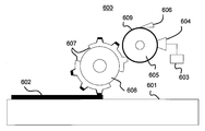
- FIG. 4 is a schematic diagram of a relief printing apparatus 600 when pattern printing is performed on an organic light emitting ink made of an organic light emitting material on a substrate 602 on which a pixel electrode 102, a hole injection layer, and a hole transport layer are formed.
- This manufacturing apparatus has a printing copper 608 on which an ink tank 603, an ink chamber 604, an anilox roll 605, and a printing plate 607 provided with a relief printing plate are mounted.
- the ink tank 603 contains organic light emitting ink diluted with a solvent, and the organic light emitting ink is fed into the ink chamber 604 from the ink tank.
- the anilox roll 605 is rotatably supported in contact with the ink supply unit of the ink chamber 604.
- the ink layer 609 of the organic light-emitting ink supplied to the surface of the anilox roll 605 is formed with a uniform film thickness.
- the ink of the ink layer 609 is transferred to the convex portion of the plate 607 mounted on the plate cylinder 608 that is driven to rotate in the vicinity of the anilox roll 605.
- the substrate to be printed 602 is installed on the stage 601, and the ink on the convex portion of the plate 607 is printed on the substrate to be printed 602, and if necessary, an organic light emitting layer is formed on the substrate to be printed 602 through a drying process. Is formed.
- the other light emitting medium layer 108 in ink it can be similarly formed using the above forming method.
- a hole blocking layer, an electron injection layer, and the like can be formed. These layers can be arbitrarily selected from the size of the organic EL display panel and the like.
- the material used for the hole blocking layer and the electron injection layer may be any material that is generally used as an electron transporting material, such as triazole, oxazole, oxadiazole, silole, and boron.
- a film can be formed by a vacuum deposition method using a material, an alkali metal such as lithium fluoride or lithium oxide, or a salt or oxide of an alkaline earth metal.
- these electron transport materials are dissolved in polymers such as polystyrene, polymethyl methacrylate, polyvinyl carbazole, and toluene, xylene, acetone, methyl ethyl ketone, methyl isobutyl ketone, cyclohexanone, methanol, ethanol, isopropyl alcohol, ethyl acetate, acetic acid. It is also possible to form an electron injection coating solution by dissolving or dispersing in butyl, water or the like alone or in a mixed solvent, and using this to form a film by a printing method.
- polymers such as polystyrene, polymethyl methacrylate, polyvinyl carbazole, and toluene, xylene, acetone, methyl ethyl ketone, methyl isobutyl ketone, cyclohexanone, methanol, ethanol, isopropyl alcohol, ethyl acetate
- the counter electrode 107 (see FIG. 5) is formed.
- the counter electrode is a cathode, a substance having a high electron injection efficiency into the light emitting layer and a low work function is used.
- a single metal such as Mg, Al, or Yb is used, or a compound such as Li, oxidized Li, or LiF is sandwiched by about 1 nm at the interface in contact with the light-emitting medium layer 108, and Al or Cu having high stability and conductivity. May be used in a stacked manner.
- one or more metals such as Li, Mg, Ca, Sr, La, Ce, Er, Eu, Sc, Y, and Yb having a low work function and stable Ag, Al
- An alloy system with a metal element such as Cu or Cu may be used.
- alloys such as MgAg, AlLi, and CuLi can be used.
- the counter electrode 107 can be formed by a resistance heating vapor deposition method, an electron beam vapor deposition method, a reactive vapor deposition method, an ion plating method, or a sputtering method, depending on the material.
- Is preferably formed over each pixel and partition as a common electrode.
- a sealing body An organic light-emitting material can be sandwiched between electrodes and an organic EL display can emit light by passing an electric current. However, since organic light-emitting materials are easily degraded by moisture and oxygen in the atmosphere, they are usually cut off from the outside.
- a sealing body is provided.
- a sealing body can be produced by providing a resin layer on a sealing material, for example.
- the sealing material it is necessary to use a base material having low moisture and oxygen permeability.
- the material include ceramics such as alumina, silicon nitride, and boron nitride, glass such as alkali-free glass and alkali glass, quartz, and moisture resistant film.
- moisture-resistant films include films formed by CVD of SiOx on both sides of plastic substrates, films with low permeability and water-absorbing films, or polymer films coated with a water-absorbing agent.
- the water vapor transmission rate is preferably 10 ⁇ 6 g / m 2 / day or less.
- Examples of the material for the resin layer include a photo-curing adhesive resin, a thermosetting adhesive resin, a two-component curable adhesive resin, and an ethylene ethyl acrylate (EEA) made of epoxy resin, acrylic resin, silicone resin, etc.
- Examples thereof include acrylic resins such as polymers, vinyl resins such as ethylene vinyl acetate (EVA), thermoplastic resins such as polyamide and synthetic rubber, and thermoplastic adhesive resins such as acid-modified products of polyethylene and polypropylene.
- Examples of methods for forming a resin layer on a sealing material include solvent solution method, extrusion lamination method, melting / hot melt method, calendar method, nozzle coating method, screen printing method, vacuum laminating method, hot roll laminating method, etc. Can be mentioned.
- the material of the resin layer can contain a material having hygroscopicity or oxygen absorption as needed.
- the thickness of the resin layer formed on the sealing material is arbitrarily determined depending on the size and shape of the organic EL display to be sealed, but is preferably about 5 to 500 ⁇ m.
- the resin layer is formed on the sealing material, but may be formed directly on the organic EL display side.
- Bonding of the organic EL display and the sealing body is performed in a sealing chamber.
- the sealing body has a two-layer structure of a sealing material and a resin layer, and a thermoplastic resin is used for the resin layer, it is preferable to perform only pressure bonding with a heated roll.
- a thermosetting adhesive resin it is preferable to perform heat curing at a curing temperature after pressure bonding with a heated roll.
- curing can be performed by further irradiating light after pressure bonding with a roll.
- Example 1 an active matrix substrate was used as the substrate. Specifically, this substrate is provided with a thin film transistor functioning as a switching element provided on a support and a pixel electrode 102 formed thereabove (see FIG. 3). Then, SiNx is formed as a protective insulating layer on the entire surface of the substrate using CVD, and an opening is formed by etching so as to expose a part of the pixel electrode 102, thereby forming a first partition 103. The light emitting area is partitioned by one partition wall 103.
- the size of the substrate is 200 ⁇ 200 mm
- the display is 5 inches diagonal
- the number of pixels is 320 ⁇ 240 dots in the center
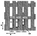
- the horizontal dimension of the SiN opening corresponds to each of R, G, B 0.03 mm, 0.03 mm, and 0.085 mm, respectively, and the vertical dimensions were all 0.2 mm (see FIG. 6) so that the light emitting area was about 1: 1: 3 for each subpixel.
- the second partition wall 105 was formed so as to partition the pixel.
- the partition walls are formed by forming a positive resist ZWD6216-6 manufactured by ZEON Corporation on the entire surface of the substrate with a spin coater to a thickness of 2 ⁇ m, and then forming a vertical width of 30 ⁇ m and a horizontal width of 100 ⁇ m at the same pitch by photolithography.
- a second partition wall 105 having a box-like shape was formed in the pixel.
- the number of subpixels of 960 ⁇ 240 dots was partitioned with an opening area of 0.09 mm ⁇ 0.26 mm by the second partition wall 105 (see FIG. 6).
- a calcium film having a thickness of 10 nm was formed as an electron injection layer by a vacuum deposition method, and then an aluminum film having a thickness of 150 nm was formed as a counter electrode 107.
- Example 2 In Example 2, as in Example 1, the active matrix substrate was used as the substrate, and the light emitting region was partitioned by the first partition 103.
- the size of the substrate is 200 x 200 mm, the diagonal 5 inches, the number of pixels is 320 x 240 dots in the center, and the size of the SiN opening corresponding to each of R, G, B
- the horizontal and vertical dimensions of the aperture are 0.035 mm ⁇ 0.18 mm, 0.045 mm ⁇ 0.22 mm, and 0.070 mm ⁇ 0, respectively, so that the light emitting area is about 1: 1.5: 3 for each pixel. .28 mm (see FIG. 7).
- a glass plate was placed as a sealing material so as to cover the entire light emitting region, and sealing was performed by thermosetting the adhesive at about 90 ° C. for 1 hour.
- the substrate was set on a sputtering film forming apparatus in which a molybdenum target was installed, and a hole injection layer was formed on the display region in a pattern so as not to be formed on the extraction electrode or the contact portion.
- the sputtering conditions at this time were a pressure of 1 Pa, a power of 1 kW, and a flow rate ratio of oxygen to argon gas of 30%.
- the film thickness was 50 nm.
- this substrate is set in a printing machine, and the direction perpendicular to the R, G, B stripes
- a hole transport layer was printed on the second electrode 105 and the pixel electrode 102 by a relief printing method in accordance with the line pattern.
- an anilox roll of 150 lines / inch was used, and a photosensitive resin relief printing plate having a width corresponding to the width of the second partition 105 was directly used.
- the film thickness of the hole transport layer after printing and drying was different for each subpixel corresponding to R, G, and B, and was 10 nm, 25 nm, and 40 nm, respectively, for the target film thickness of 20 nm.
- this substrate is set in a printing machine, and is aligned with the line pattern directly above the pixel electrode 102.
- the organic light emitting layer was printed by a relief printing method.
- the width of the convex portion corresponding to the opening width defined by the second partition 105 of the R, G, and B sub-pixels is 1: 1.5: 3, respectively.
- the photosensitive resin plate letterpress was used.
- the film thickness of the organic light emitting layer after drying was 80 nm. Through this process, an organic light emitting layer corresponding to the emission colors of R, G, and B was formed in each pixel. The film thickness abnormality partially occurred due to the effect that the hole transport material was unevenly formed on the partition wall.
- a calcium film having a thickness of 10 nm was formed as an electron injection layer by a vacuum evaporation method, and then an aluminum film having a thickness of 150 nm was formed as a counter electrode.
- the film thickness of the hole transport material is Each color was different, and the characteristics of each color could not be sufficiently obtained, and the luminous efficiency when the entire surface was turned on was reduced by about 25% compared to Examples 1 and 2. In addition, unevenness of roughness due to a partial abnormality in the light emitting layer thickness occurred.
Landscapes
- Engineering & Computer Science (AREA)
- Manufacturing & Machinery (AREA)
- Microelectronics & Electronic Packaging (AREA)
- Electroluminescent Light Sources (AREA)
Abstract
【課題】有機ELディスプレイにおいて、発光輝度の寿命の改善と表示品質の向上を両立させることが可能な、有機ELディスプレイとその製造方法を提供することを目的とする。 【解決手段】第一電極を第一隔壁で少なくとも2つの異なる開口面積で区画することで発光面積を制御し、第二隔壁で区画された最大の開口面積と最小の開口面積の面積比率を、第一隔壁で区画された最大の開口面積と最小の開口面積の面積比率よりも小さくすることによって各色の第二隔壁で区画された開口面積をできるだけ揃えることで、発光媒体層用インキを均一に形成するこが可能となり、発光輝度の寿命改善と表示品質を向上させることができる有機ELディスプレイとその製造方法を提供する。
Description
本発明は有機エレクトロルミネッセンスディスプレイとその製造方法に関するものである。
有機エレクトロルミネッセンス素子(以下、有機EL素子)は、二つの対向する電極の間に有機発光材料からなる有機発光層が形成され、有機発光層に電流を流すことで発光させるものであるが、効率よくかつ信頼性のある素子を作製するには有機発光層の膜厚が重要である。また、これを用いて有機エレクトロルミネッセンスディスプレイ(以下、適宜「有機ELディスプレイ」と略称することがある)を製造するには、有機EL素子自体を高精細にパターニングする必要がある。
一般的に、有機ELディスプレイ用の基板としては、パターニングされた感光性ポリイミド樹脂あるいは、感光性ノボラック系レジストなどがサブピクセルを区画するように隔壁状に形成されたものが用いられる。その際、隔壁パターンは陽極として成膜されている透明電極のエッジ部を覆うように形成される。
次に正孔キャリアを注入するための正孔注入層を成膜する方法としては、ドライ成膜法とウェット成膜法の2種類があるが、ウェット成膜法を用いる場合、一般的に水に分散されたポリチオフェンの誘導体が用いられる。ドライ成膜法を用いる場合、正孔輸送能力を有した有機材料や金属酸化物などの無機物が蒸着法やスパッタリング法を用いて成膜される。ドライコーティングの場合は比較的簡便に均一に全面コーティングが可能である。
次に電極から正孔注入層に注入された正孔の発光層へのスムーズな注入と、後に成膜する対向電極から注入される電子が正孔輸送層に流れ込まないように発光層界面でせき止める役割として、正孔注入層と発光層との間に正孔輸送層が形成される。形成方法としては正孔注入層と同様である。
有機発光層を形成する方法も同様にドライ成膜法とウェット成膜法の2種類があるが、均一な成膜が容易なドライ成膜法である真空蒸着法を用いる場合、微細パターンのマスクを用いてパターニングする必要があり、大型基板や微細パターニングが非常に困難である。
そこで、最近では高分子材料を溶剤に溶かして塗工液にし、これをウェット成膜法で薄膜形成する方法が試みられるようになってきている。高分子材料の塗工液を用いてウェット成膜法で有機発光層を含む発光媒体層を形成する場合の層構成は、陽極側から順に正孔輸送層、有機発光層と積層する2層構成が一般的である。このとき、有機発光層はカラーパネル化するために赤(R)、緑(G)、青(B)のそれぞれの発光色をもつ有機発光材料を溶剤中に溶解または安定に分散させた有機発光インキを用いて塗り分けることができる(特許文献1参照)。
電極の間には有機発光層以外にもキャリア注入層(キャリア輸送層とも呼ばれる)が形成される。キャリア注入層とは電極から有機発光層へ電子を注入させる際に、電子の注入量を制御あるいは、もう一方の電極から有機発光層へ正孔が注入される際に、正孔の注入量を制御するのに用いられる層で、電極と有機発光層の間に挿入される層を指す。キャリア注入層のうち電子の注入量を制御するのに用いられる電子注入層としては、キノリノール誘導体の金属錯体などの電子輸送性の有機物や、Ca、Baなどの仕事関数の比較的小さい例えばアルカリ金属などが用いられ、あるいはこれらの機能を持つ層を複数積層するものが用いられる場合もある。
一般的な有機ELディスプレイの構造において、1ピクセル中のR、G、B各サブピクセルは、上述したように感光性ポリイミド、あるいは感光性ノボラック系レジストで形成された隔壁によって同形、同面積になるように区画されている。この場合、一般的にはR、G、Bそれぞれの輝度半減時間が異なるため、長時間ディスプレイを駆動すると色バランスが変化し動画の色味が変化してしまうという問題があった。
また、有機ELディスプレイにおいて、1ピクセル中のR、G、B各サブピクセルは、上述したように感光性ポリイミド、あるいは感光性ノボラック系、あるいは感光性アクリル系材料で形成された隔壁によって区画され、通常区画されるサブピクセルの発光領域は同形、同面積でレイアウトされている。しかし、一般的にはR、G、Bそれぞれの輝度半減時間が異なるため、長時間ディスプレイを駆動すると色バランスが変化し発光色が変化してしまうという問題がある。これを解決する手段として図2のように、R、G、Bそれぞれの輝度半減特性に応じて、サブピクセルの面積を隔壁によってある比率に区画することで、色の変化、輝度半減時間の改善を図る手法がとられている(例えば、特許文献1参照)。ここに、図2(a)は平面図、図2(b)は図2(a)のX-Y断面図である。
ところで、特許文献1に記載されているような有機ELディスプレイにおいて、サブピクセルの発光領域を決定する役割を担う隔壁の直上に開口領域の異なるもう一つの隔壁(第二の隔壁)は無く、隔壁の高さが1μm以下程度の場合、印刷でR、G、Bをそれぞれライン状に印刷パターニングする際に混色の問題が生じる。また、この隔壁の高さが1μm以上の場合は印刷方式でR、G、Bラインと垂直な方向に共通層をライン成膜する際に、隔壁幅が異なるため隔壁に取られるインキ量の制御が難しく、各発光領域に流れ込むインキ量が異なりR、G、B各サブピクセル間で同じ膜厚にならず、発光特性が悪くなるという問題が生じる。
それ故に、本発明の主たる目的は、各色のサブピクセルの面積が異なっても、発光特性の良好な有機エレクトロルミネッセンスディスプレイパネルとその製造方法を提供することである。
本発明は、上述の課題を解決するために、以下の構成を採用した。
本発明に係る有機エレクトロルミネッセンスディスプレイパネルの製造方法は、基板上に画素ごとに第一電極を形成するステップと、第一電極を少なくとも2つの異なる開口面積に区画する第一隔壁を形成する第一隔壁形成ステップと、第一隔壁の上に、画素を少なくとも2つの異なる開口面積で区画する第二隔壁を形成する第二隔壁形成ステップと、発光媒体層の一部をウェット成膜法により形成する発光媒体層形成ステップとを備え、第二隔壁形成ステップでは、第二隔壁によって区画される最大の開口面積と最小の開口面積の面積比率が、第一隔壁で区画された最大の開口面積と最小の開口面積の面積比率よりも小さくなるように、第二隔壁を形成する。
また、第一隔壁形成ステップでは、第一隔壁の高さが1μm以下になるように第一隔壁を形成してもよい。
また、第二隔壁形成ステップでは、第二隔壁の高さが1μm以上になるように第二隔壁を形成してもよい。
また、第二隔壁形成ステップでは、第二隔壁で区画される最大の開口面積と最小の開口面積の面積比率が2:1以下になるように、第二隔壁を形成してもよい。
また、発光媒体層は有機発光層であり、発光媒体層形成ステップでは、ウェット成膜法として凸版印刷法、インクジェット法、ノズルプリント法のいずれかを用いてもよい。
以上では、有機エレクトロルミネッセンスディスプレイパネルの製造方法として本発明を構成する場合について記載した。しかし、本発明は、有機エレクトロルミネッセンスディスプレイ、有機エレクトロルミネッセンス素子等として構成されてもよい。
上記した構成によれば、有機エレクトロルミネッセンスディスプレイパネル(有機ELディスプレイパネル)において第一隔壁で区画された異なる色のサブピクセル間の開口面積の比率よりも小さくなるように、第二隔壁で区画される異なる色のサブピクセル間の開口面積をできるだけ揃えるように配置した隔壁付き基板が形成される。このことにより、印刷方式を用いてR、G、Bのラインパターンを印刷する際に、第二隔壁があることで混色を防ぎ、かつ同じストライプ版、同等の粘度をもつインキを用いて安定した印刷が可能となる。更に、キャリア輸送層などの共通層をR、G、Bのストライプと垂直方向にライン状に印刷する際に、第二隔壁の開口面積がほぼ同等に設定されることにより、第二隔壁で区画された領域に均一にインキが入り、面積の異なる発光領域に均等にインキが入ることで同じ膜厚での安定した成膜が可能となり、隔壁上に形成される膜も均一となるため次に印刷される発光層が均一な膜厚、形状で形成が可能となる。以上より、本発明によれば、各色のサブピクセル面積が異なっても、発光特性の良好な有機ELディスプレイパネルの製造方法等を提供することが可能となる。
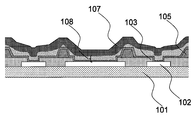
図1及び図5を参照しつつ、本発明の一実施形態である有機ELディスプレイについて説明する。図1は、本実施形態の有機ELディスプレイに用いられる隔壁付き基盤を示す図であって、図1(a)は平面図、図1(b)は図1(a)のX-Y線に沿った断面図であり、図5は、図1(b)に示す断面図の詳細を示す断面図である。本実施形態の有機EL素子は、基板101上に形成された第一電極102(以下、画素電極102ということがある)と、これと対向するように形成された第二電極107(以下、対向電極107ということがある)とに挟持された層(発光媒体層108)を有している。発光媒体層108には、少なくとも発光に寄与する有機発光層と、電子あるいは正孔を注入するキャリア注入層と、キャリア注入層から電子あるいは正孔を発光層へ輸送するためのキャリア輸送層を含んでいる。発光媒体層108は、陰極と発光層の間に電子注入層や正孔ブロック層(電子輸送層)、陽極と発光層の間に正孔注入層や電子ブロック層(正孔輸送層)等を必要に応じて積層することにより形成される。
さらに本実施形態の有機EL素子は有機発光層を区画する第一隔壁103を有し、その上に第二隔壁105を有する。このような有機EL素子を画素(サブピクセル)として配列することにより、有機ELディプレイとすることができる。各画素を構成する発光層を例えばR、G、Bの3色に塗り分けることで、フルカラーの有機ELディスプレイパネルを作製することができる。また、全面が白色で発光するように白色に発光するような発光材料または、少なくとも2色以上に発光する層の積層構造を表示領域全面に成膜し、カラーフィルタを用いてカラー化することでフルカラーの有機ELディスプレイパネルを作製することができる。
以下、本実施形態の有機ELディスプレイの構成について詳細に説明する。本実施形態の有機ELディスプレイの説明をするための例として、第一電極102を陽極、第二電極107を陰極としたアクティブマトリクス駆動型有機ELディスプレイについて述べる(図5参照)。この場合には、第一電極102は画素ごとに第一隔壁103で区画された画素電極として形成される。第二隔壁105は、第一隔壁103に接するように設置される。また、キャリア注入層のうち、第一電極102側に形成される第一キャリア注入層は正孔輸送性の正孔注入層となる。また第一電極102側を陰極とした逆構造の有機EL素子としてもよい。この場合には第一キャリア注入層は電子輸送性の電子注入層となる。
<基板>
図3に本実施形態の有機ELディスプレイに用いられる隔壁付きTFT基板の例を示す。本実施形態のアクティブマトリクス駆動型有機ELディスプレイに用いる基板(バックプレーン)308には、薄膜トランジスタ(TFT)と有機EL表示装置の下部電極(画素電極102)とが設けられており、かつ、TFTと下部電極とが電気的に接続している。
図3に本実施形態の有機ELディスプレイに用いられる隔壁付きTFT基板の例を示す。本実施形態のアクティブマトリクス駆動型有機ELディスプレイに用いる基板(バックプレーン)308には、薄膜トランジスタ(TFT)と有機EL表示装置の下部電極(画素電極102)とが設けられており、かつ、TFTと下部電極とが電気的に接続している。
TFTや、その上方に構成されるアクティブマトリクス駆動型有機ELディスプレイは支持体で支持される。支持体としては機械的強度、絶縁性を有し寸法安定性に優れた支持体であれば如何なる材料も使用することができる。例えば、ガラスや石英、ポリプロピレン、ポリエーテルサルフォン、ポリカーボネート、シクロオレフィンポリマー、ポリアリレート、ポリアミド、ポリメチルメタクリレート、ポリエチレンテレフタレート、ポリエチレンナフタレート等のプラスチックフィルムやシート、または、これらプラスチックフィルムやシートに酸化珪素、酸化アルミニウム等の金属酸化物や、弗化アルミニウム、弗化マグネシウム等の金属弗化物、窒化珪素、窒化アルミニウムなどの金属窒化物、酸窒化珪素などの金属酸窒化物、アクリル樹脂やエポキシ樹脂、シリコーン樹脂、ポリエステル樹脂などの高分子樹脂膜を単層もしくは積層させた透光性基材や、アルミニウムやステンレスなどの金属箔、シート、板や、前記プラスチックフィルムやシートにアルミニウム、銅、ニッケル、ステンレスなどの金属膜を積層させた非透光性基材などを用いることができる。光取出しをどちらの面から行うかに応じて支持体の透光性を選択すればよい。これらの材料からなる支持体は、有機EL表示装置内への水分の侵入を避けるために、無機膜を形成したり、フッ素樹脂を塗布したりして、防湿処理や疎水性処理を施してあることが好ましい。特に、発光媒体層108への水分の侵入を避けるために、支持体における含水率およびガス透過係数を小さくすることが好ましい。
支持体上に設ける薄膜トランジスタは、公知の薄膜トランジスタを用いることができる。具体的には、図3に示すように、主として、ソース/ドレイン領域及びチャネル領域が形成される活性層311、ゲート絶縁膜309及びゲート電極314から構成される薄膜トランジスタが挙げられる。薄膜トランジスタの構造としては、特に限定されるものではなく、例えば、スタガ型、逆スタガ型、トップゲート型、コプレーナ型等が挙げられる。
活性層311は、特に限定されるものではなく、例えば、非晶質シリコン、多結晶シリコン、微結晶シリコン、セレン化カドミウム等の無機半導体材料又はチオフエンオリゴマー、ポリ(p-フェリレンビニレン)等の有機半導体材料により形成することができる。
これらの活性層311を形成する方法には、例えば、アモルファスシリコンをプラズマCVD法により積層し、イオンドーピングする方法;SiH4ガスを用いてLPCVD法によりアモルファスシリコンを形成し、固相成長法によりアモルファスシリコンを結晶化してポリシリコンを得た後、イオン打ち込み法によりイオンドーピングする方法;Si2H6ガスを用いてLPCVD法により、また、SiH4ガスを用いてPECVD法によりアモルファスシリコンを形成し、エキシマレーザー等のレーザーによりアニールし、アモルファスシリコンを結晶化してポリシリコンを得た後、イオンドーピング法によりイオンドーピングする方法(低温プロセス);減圧CVD法又はLPCVD法によりポリシリコンを積層し、1000℃以上で熱酸化してゲート絶縁膜を形成し、その上にn+ポリシリコンのゲート電極8を形成し、その後、イオン打ち込み法によりイオンドーピングする方法(高温プロセス)等が挙げられる。
これらの活性層311を形成する方法には、例えば、アモルファスシリコンをプラズマCVD法により積層し、イオンドーピングする方法;SiH4ガスを用いてLPCVD法によりアモルファスシリコンを形成し、固相成長法によりアモルファスシリコンを結晶化してポリシリコンを得た後、イオン打ち込み法によりイオンドーピングする方法;Si2H6ガスを用いてLPCVD法により、また、SiH4ガスを用いてPECVD法によりアモルファスシリコンを形成し、エキシマレーザー等のレーザーによりアニールし、アモルファスシリコンを結晶化してポリシリコンを得た後、イオンドーピング法によりイオンドーピングする方法(低温プロセス);減圧CVD法又はLPCVD法によりポリシリコンを積層し、1000℃以上で熱酸化してゲート絶縁膜を形成し、その上にn+ポリシリコンのゲート電極8を形成し、その後、イオン打ち込み法によりイオンドーピングする方法(高温プロセス)等が挙げられる。
ゲート絶縁膜309としては、通常、ゲート絶縁膜として使用されているものを用いることができ、例えば、PECVD法、LPCVD法等により形成されたSiO2や、ポリシリコン膜を熱酸化して得られるSiO2等を用いることができる。
ゲート電極314としては、通常、ゲート電極として使用されているものを用いることができ、例えば、アルミ、銅等の金属;チタン、タンタル、タングステン等の高融点金属;ポリシリコン;高融点金属のシリサイド;ポリサイド;等を用いることができる。
薄膜トランジスタは、シングルゲート構造、ダブルゲート構造、ゲート電極が3つ以上のマルチゲート構造であってもよい。また、LDD構造、オフセット構造を有していてもよい。さらに、1つの画素中に2つ以上の薄膜トランジスタが配置されていてもよい。
本実施形態の有機ELディスプレイは、薄膜トランジスタが有機ELディスプレイのスイッチング素子として機能するように接続されている必要があり、トランジスタのドレイン電極310と有機ELディスプレイの画素電極102が電気的に接続されている。
<画素電極>
TFT付き基板308の上に画素電極102を成膜し、必要に応じてパターニングをおこなう。本実施形態では、画素電極102は第一隔壁103によって区画され、さらに、各画素は第一隔壁103上に形成された第二隔壁105によって区画され、各画素に対応した画素電極となる。画素電極102の材料としては、ITO(インジウムスズ複合酸化物)やインジウム亜鉛複合酸化物、亜鉛アルミニウム複合酸化物などの金属複合酸化物や、金、白金などの金属材料や、これら金属酸化物や金属材料の微粒子をエポキシ樹脂やアクリル樹脂などに分散した微粒子分散膜を、単層もしくは積層したものをいずれも使用することができる。画素電極102を陽極とする場合にはITOなど仕事関数の高い材料を選択することが好ましい。下方から光を取り出す、いわゆるボトムエミッション構造の場合は透光性のある材料を選択する必要がある。必要に応じて、画素電極102の配線抵抗を低くするために、銅やアルミニウムなどの金属材料を補助電極として併設してもよい。
画素電極102の形成方法としては、材料に応じて、抵抗加熱蒸着法、電子ビーム蒸着法、反応性蒸着法、イオンプレーティング法、スパッタリング法などの乾式成膜法や、グラビア印刷法、スクリーン印刷法などの湿式成膜法を用いることができる。画素電極102のパターニング方法としては、材料や成膜方法に応じて、マスク蒸着法、フォトリソグラフィー法、ウェットエッチング法、ドライエッチング法などの既存のパターニング法を用いることができる。基板としてTFTを形成した物を用いる場合は下層の画素に対応して導通を図ることができるように形成する。
TFT付き基板308の上に画素電極102を成膜し、必要に応じてパターニングをおこなう。本実施形態では、画素電極102は第一隔壁103によって区画され、さらに、各画素は第一隔壁103上に形成された第二隔壁105によって区画され、各画素に対応した画素電極となる。画素電極102の材料としては、ITO(インジウムスズ複合酸化物)やインジウム亜鉛複合酸化物、亜鉛アルミニウム複合酸化物などの金属複合酸化物や、金、白金などの金属材料や、これら金属酸化物や金属材料の微粒子をエポキシ樹脂やアクリル樹脂などに分散した微粒子分散膜を、単層もしくは積層したものをいずれも使用することができる。画素電極102を陽極とする場合にはITOなど仕事関数の高い材料を選択することが好ましい。下方から光を取り出す、いわゆるボトムエミッション構造の場合は透光性のある材料を選択する必要がある。必要に応じて、画素電極102の配線抵抗を低くするために、銅やアルミニウムなどの金属材料を補助電極として併設してもよい。
画素電極102の形成方法としては、材料に応じて、抵抗加熱蒸着法、電子ビーム蒸着法、反応性蒸着法、イオンプレーティング法、スパッタリング法などの乾式成膜法や、グラビア印刷法、スクリーン印刷法などの湿式成膜法を用いることができる。画素電極102のパターニング方法としては、材料や成膜方法に応じて、マスク蒸着法、フォトリソグラフィー法、ウェットエッチング法、ドライエッチング法などの既存のパターニング法を用いることができる。基板としてTFTを形成した物を用いる場合は下層の画素に対応して導通を図ることができるように形成する。
<隔壁>
本実施形態では、第一隔壁103は画素に対応した発光領域を区画するように形成される。第一隔壁103は画素電極102の端部を覆うように形成されるのが好ましい。また、第二隔壁105は第一隔壁103の上に形成される。一般的にアクティブマトリクス駆動型の表示装置は各画素(サブピクセル)に対して画素電極102が形成され、それぞれの画素ができるだけ広い面積を占有しようとするため、第一隔壁103が画素電極102の端部を覆うように形成され、隔壁の最も好ましい形状は各画素電極102を最短距離で区切る格子状を基本とする。
本実施形態では、第一隔壁103は画素に対応した発光領域を区画するように形成される。第一隔壁103は画素電極102の端部を覆うように形成されるのが好ましい。また、第二隔壁105は第一隔壁103の上に形成される。一般的にアクティブマトリクス駆動型の表示装置は各画素(サブピクセル)に対して画素電極102が形成され、それぞれの画素ができるだけ広い面積を占有しようとするため、第一隔壁103が画素電極102の端部を覆うように形成され、隔壁の最も好ましい形状は各画素電極102を最短距離で区切る格子状を基本とする。
第一、第二隔壁の形成方法としては、従来と同様、基体上に無機膜を一様に形成し、レジストでマスキングした後、ドライエッチングを行う方法や、基体上に感光性樹脂を積層し、フォトリソ法により所定のパターンとする方法が挙げられ、第一、第二隔壁は無機膜又は感光性樹脂のいずれを用いても良い。必要に応じて撥水剤を添加したり、プラズマやUVを照射して形成後にインクに対する撥液性を付与することもできる。
本発明においては、第二隔壁によって区画される最大の開口面積と最小の開口面積の面積比率が、第一隔壁によって区画される最大の開口面積と最小の開口面積の面積比率よりも小さくなるように形成される。
本発明においては、第二隔壁によって区画される最大の開口面積と最小の開口面積の面積比率が、第一隔壁によって区画される最大の開口面積と最小の開口面積の面積比率よりも小さくなるように形成される。
第一隔壁103の好ましい高さは0.1μm以上2μm以下であり、より好ましくは0.5μm以上1μm以下である。本発明においては、第一隔壁により1ピクセルを構成するサブピクセルの発光面積が規定され、また、第一隔壁はR、G、Bの各色のサブピクセルごとに開口幅が異なるように形成されている。輝度半減特性が短い色の開口幅を広くすることで、色の変化が起こりにくく、輝度半減時間を長くすることができる。R、G、Bのサブピクセルの開口面積は、各色毎に開口面積が異なっていても、1色だけ異なっていても良い。
本発明では、有機発光インキは後述の第二隔壁105により区画されるため、第一隔壁103が区画する画素電極上だけでなく第一隔壁103上にもキャリア注入層、正孔輸送層、有機発光層等の発光媒体層が形成される。また、第一隔壁103が発光面積を規定するよう形成されるため、第一隔壁103の幅は第二隔壁105の幅よりも大きくなる。
本発明では、有機発光インキは後述の第二隔壁105により区画されるため、第一隔壁103が区画する画素電極上だけでなく第一隔壁103上にもキャリア注入層、正孔輸送層、有機発光層等の発光媒体層が形成される。また、第一隔壁103が発光面積を規定するよう形成されるため、第一隔壁103の幅は第二隔壁105の幅よりも大きくなる。
第二隔壁105は発光色の異なる有機発光材料が混色するのを防ぐため、第二隔壁105の好ましい高さは0.5μm以上10μm以下であり、より好ましくは1μm以上5μm以下である。
本発明においては、第二隔壁105は異なる色のサブピクセル間の開口面積が同一になるように配置され、少なくとも、第二隔壁で区画される最大の開口面積が、第二隔壁で区画される最小の開口面積の2倍以下になるように配置されるのが望ましい。
本発明においては、第二隔壁105は異なる色のサブピクセル間の開口面積が同一になるように配置され、少なくとも、第二隔壁で区画される最大の開口面積が、第二隔壁で区画される最小の開口面積の2倍以下になるように配置されるのが望ましい。
上述の通り、本発明では第一隔壁103で区画される開口面積は色毎に異なり、第二隔壁105で区画される最大の開口面積は第二隔壁で区画される最小の開口面積の2倍以下であるため、第二隔壁105によって区画される最大の開口面積と最小の開口面積の面積比率が、第一隔壁103によって区画される最大の開口面積と最小の開口面積の面積比率よりも小さくなる。
これにより、印刷方式を用いてR、G、Bのラインパターンを印刷する際に、第一隔壁103によって区画される発光面積が色ごとに異なっていても、第二隔壁105で区画される色ごとの開口面積の差が少ないため、発光面積の異なるサブピクセルであっても第二隔壁内に塗布されるインキ量の変化が少なく、また、異なる色ごとの第二隔壁表面に濡れ広がるインキの量の変化が少なく、同じストライプ版、同等の粘度をもつインキを用いて安定した印刷が可能となる。
更に、キャリア輸送層などの共通層をR、G、Bのストライプと直交する方向にライン状に印刷する際に、第二隔壁の開口面積がほぼ同等に設定されることにより、第二隔壁で区画された領域に均一にインキが入り、面積の異なる発光領域に均等にインキが入ることで共通層を同じ膜厚で成膜することが可能となり、隔壁上に形成される膜も均一となるため次に印刷される発光層が均一な膜厚、形状で形成が可能となる。
なお、同色の有機発光層を印刷法で形成する場合にはストライプ状に第二隔壁105をまたがって形成されるため、同色の画素を区画している第二隔壁(図1の104)は異なる色を区画する第二隔壁の高さ(図1の縦方向)よりも低くても良い。
更に、キャリア輸送層などの共通層をR、G、Bのストライプと直交する方向にライン状に印刷する際に、第二隔壁の開口面積がほぼ同等に設定されることにより、第二隔壁で区画された領域に均一にインキが入り、面積の異なる発光領域に均等にインキが入ることで共通層を同じ膜厚で成膜することが可能となり、隔壁上に形成される膜も均一となるため次に印刷される発光層が均一な膜厚、形状で形成が可能となる。
なお、同色の有機発光層を印刷法で形成する場合にはストライプ状に第二隔壁105をまたがって形成されるため、同色の画素を区画している第二隔壁(図1の104)は異なる色を区画する第二隔壁の高さ(図1の縦方向)よりも低くても良い。
次に、画素電極上に形成される発光媒体層を構成する各層について説明する。発光媒体層はキャリア注入層、正孔輸送層、有機発光層、電子注入層を含む。
<キャリア注入層>
本実施形態では、キャリア注入層は電極を覆うように所定のパターンあるいは全面に成膜される。例えば、キャリア注入層を形成する1つである正孔注入層に用いる材料としては、ポリアニリン誘導体、ポリチオフェン誘導体、ポリビニルカルバゾール(PVK)誘導体、ポリ(3,4-エチレンジオキシチオフェン)(PEDOT)等を用いることができる。これらの材料を溶媒に溶解または分散させ、スピンコーター等を用いた各種塗布方法や凸版印刷方法を用いることによって、正孔注入層が形成される。
本実施形態では、キャリア注入層は電極を覆うように所定のパターンあるいは全面に成膜される。例えば、キャリア注入層を形成する1つである正孔注入層に用いる材料としては、ポリアニリン誘導体、ポリチオフェン誘導体、ポリビニルカルバゾール(PVK)誘導体、ポリ(3,4-エチレンジオキシチオフェン)(PEDOT)等を用いることができる。これらの材料を溶媒に溶解または分散させ、スピンコーター等を用いた各種塗布方法や凸版印刷方法を用いることによって、正孔注入層が形成される。
また正孔注入層に用いる材料として無機材料を用いる場合、無機材料としては、Cu2O,Cr2O3,Mn2O3,FeOx(x~0.1),NiO,CoO,Pr2O3,Ag2O,MoO2,Bi2O3、ZnO,TiO2,SnO2,ThO2,V2O5,Nb2O5,Ta2O5,MoO3,WO3,MnO2等の遷移金属酸化物およびこれらの窒化物、硫化物を一種以上含んだ無機化合物を用いることができる。ただし材料はこれらに限定されるものではない。無機材料は耐熱性および電気化学的安定性に優れている材料が多いため好ましい。これらを単層もしくは複数の層の積層構造、又は混合層とすることによって、正孔注入層を形成することができる。正孔注入層の好ましい膜厚は5nm以上であり、より好ましくは15nm程度以上である。正孔注入層の形成法としては、材料に応じて、抵抗加熱蒸着法、電子ビーム蒸着法、反応性蒸着法、イオンプレーティング法、スパッタリング法などのドライ成膜法や、スピンコート法、ゾルゲル法、などのウェット成膜法など既存の成膜法を用いることができるが本実施形態ではこれらに限定されず、一般的な成膜法を用いることができる。
<正孔輸送層>
キャリア注入層(正孔注入層)形成後、更に正孔輸送層を形成することができる。正孔輸送層に用いる材料としては、キャリア注入層として記載の上記の材料や、ポリビニルカルバゾール若しくはその誘導体、側鎖若しくは主鎖に芳香族アミンを有するポリアリーレン誘導体、アリールアミン誘導体、トリフェニルジアミン誘導体などの、芳香族アミンを含むポリマー等を用いることができる。これらの材料を溶媒に溶解または分散させ、スピンコーター等を用いた各種塗布方法や凸版印刷方法を用いることによって、正孔輸送層が形成される。
凸版印刷方法で正孔輸送層を形成する際、R、G、Bサブピクセルのラインと直交する方向に形成することが望ましい。R、G、Bサブピクセルのラインと直交する方向のサブピクセル幅は、R、G、Bサブピクセルのラインと平行な方向よりも幅が広く、凸版の凸部が形成しやすい。また、R、G、Bのサブピクセルを一括して塗布できるのでプロセスの簡略化が可能となる。
キャリア注入層(正孔注入層)形成後、更に正孔輸送層を形成することができる。正孔輸送層に用いる材料としては、キャリア注入層として記載の上記の材料や、ポリビニルカルバゾール若しくはその誘導体、側鎖若しくは主鎖に芳香族アミンを有するポリアリーレン誘導体、アリールアミン誘導体、トリフェニルジアミン誘導体などの、芳香族アミンを含むポリマー等を用いることができる。これらの材料を溶媒に溶解または分散させ、スピンコーター等を用いた各種塗布方法や凸版印刷方法を用いることによって、正孔輸送層が形成される。
凸版印刷方法で正孔輸送層を形成する際、R、G、Bサブピクセルのラインと直交する方向に形成することが望ましい。R、G、Bサブピクセルのラインと直交する方向のサブピクセル幅は、R、G、Bサブピクセルのラインと平行な方向よりも幅が広く、凸版の凸部が形成しやすい。また、R、G、Bのサブピクセルを一括して塗布できるのでプロセスの簡略化が可能となる。
<有機発光層>
正孔輸送層を形成後、有機発光層を形成する。有機発光層は電流を通すことにより発光する層であり、有機発光層から放出される表示光が単色の場合、正孔輸送層を被覆するように形成されるが、多色の表示光を得るには必要に応じてパターニングを行うことにより好適に形成される。
正孔輸送層を形成後、有機発光層を形成する。有機発光層は電流を通すことにより発光する層であり、有機発光層から放出される表示光が単色の場合、正孔輸送層を被覆するように形成されるが、多色の表示光を得るには必要に応じてパターニングを行うことにより好適に形成される。
有機発光層を形成する有機発光材料は、例えばクマリン系、ペリレン系、ピラン系、アンスロン系、ポルフィレン系、キナクリドン系、N,N’-ジアルキル置換キナクリドン系、ナフタルイミド系、N,N’-ジアリール置換ピロロピロール系、イリジウム錯体系などの発光性色素をポリスチレン、ポリメチルメタクリレート、ポリビニルカルバゾール等の高分子中に分散させたものや、ポリアリーレン系、ポリアリーレンビニレン系やポリフルオレン系の高分子材料が挙げられるが本実施形態ではこれらに限定されるわけではない。
これらの有機発光材料は溶媒に溶解または安定に分散させ有機発光インキとなる。有機発光材料を溶解または分散する溶媒としては、トルエン、キシレン、アセトン、アニソール、メチルエチルケトン、メチルイソブチルケトン、シクロヘキサノンなどの単独またはこれらの混合溶媒が挙げられる。中でもトルエン、キシレン、アニソールといった芳香族有機溶媒が有機発光材料の溶解性の面から好適である。また、有機発光インキには必要に応じて、界面活性剤、酸化防止剤、粘度調整剤、紫外線吸収剤等が添加されてもよい。
上述した高分子材料に加え、9,10-ジアリールアントラセン誘導体、ピレン、コロネン、ペリレン、ルブレン、1,1,4,4-テトラフェニルブタジエン、トリス(8-キノラート)アルミニウム錯体、トリス(4-メチル-8-キノラート)アルミニウム錯体、ビス(8-キノラート)亜鉛錯体、トリス(4-メチル-5-トリフルオロメチル-8-キノラート)アルミニウム錯体、トリス(4-メチル-5-シアノ-8-キノラート)アルミニウム錯体、ビス(2-メチル-5-トリフルオロメチル-8-キノリノラート)[4-(4-シアノフェニル)フェノラート]アルミニウム錯体、ビス(2-メチル-5-シアノ-8-キノリノラート)[4-(4-シアノフェニル)フェノラート]アルミニウム錯体、トリス(8-キノリノラート)スカンジウム錯体、ビス[8-(パラ-トシル)アミノキノリン]亜鉛錯体及びカドミウム錯体、1,2,3,4-テトラフェニルシクロペンタジエン、ポリ-2,5-ジヘプチルオキシ-パラ-フェニレンビニレンなどの低分子系発光材料を有機発光材料として使用することができる。
有機発光層の形成法としては、材料に応じて、抵抗加熱蒸着法、電子ビーム蒸着法、反応性蒸着法、イオンプレーティング法、スパッタリング法などのドライ成膜法や、インクジェット印刷法、凸版印刷法、グラビア印刷法、スクリーン印刷法、ノズルプリント印刷法などのウェット成膜法など既存の成膜法を用いることができ、これらを組み合わせても良い。本実施形態ではこれらに限定されるわけではないが、ウェット成膜法を用いることが好ましい。
<発光媒体層の形成方法>
塗布法で発光媒体層108を形成する場合、下記凸版印刷法を用いることができる。特に有機発光材料を溶媒に溶解または安定に分散させた有機発光インキを用いて発光層を各発光色に塗り分ける場合には、隔壁間にインキを転写してパターニングできる凸版印刷法が好適である。
塗布法で発光媒体層108を形成する場合、下記凸版印刷法を用いることができる。特に有機発光材料を溶媒に溶解または安定に分散させた有機発光インキを用いて発光層を各発光色に塗り分ける場合には、隔壁間にインキを転写してパターニングできる凸版印刷法が好適である。
図4に有機発光材料からなる有機発光インキを、画素電極102、正孔注入層、及び正孔輸送層が形成された被印刷基板602上にパターン印刷する際の凸版印刷装置600の概略図を示した。本製造装置は、インクタンク603とインキチャンバー604とアニロックスロール605と凸版が設けられた版607がマウントされた版銅608を有している。インクタンク603には、溶剤で希釈された有機発光インキが収容されており、インキチャンバー604にはインクタンクより有機発光インキが送り込まれるようになっている。アニロックスロール605はインキチャンバー604のインキ供給部に接して回転可能に支持されている。
アニロックスロール605の回転に伴い、アニロックスロール605の表面に供給された有機発光インキのインキ層609は均一な膜厚に形成される。このインキ層609のインキはアニロックスロール605に近接して回転駆動される版胴608にマウントされた版607の凸部に転移する。被印刷基板602は、ステージ601の上に設置され、版607の凸部にあるインキが被印刷基板602に対して印刷され、必要に応じて乾燥工程を経て被印刷基板602上に有機発光層が形成される。
他の発光媒体層108をインキ化して塗工する場合についても同様に上記形成法を用いて形成することができる。
<電子注入層>
有機発光層を形成した後、正孔ブロック層や電子注入層等を形成することができる。これらの層は、有機ELディスプレイパネルの大きさ等から任意に選択することができる。
正孔ブロック層および電子注入層に用いる材料としては、一般に電子輸送材料として用いられているものであれば良く、トリアゾール系、オキサゾール系、オキサジアゾール系、シロール系、ボロン系等の低分子系材料、フッ化リチウムや酸化リチウム等のアルカリ金属やアルカリ土類金属の塩や酸化物等を用いて真空蒸着法による成膜が可能である。また、これらの電子輸送性材料をポリスチレン、ポリメチルメタクリレート、ポリビニルカルバゾール等の高分子中に溶解させトルエン、キシレン、アセトン、メチルエチルケトン、メチルイソブチルケトン、シクロヘキサノン、メタノール、エタノール、イソプロピルアルコール、酢酸エチル、酢酸ブチル、水等の単独または混合溶媒に溶解または分散させて電子注入塗布液とし、これを用いて印刷法により成膜することも可能である。
有機発光層を形成した後、正孔ブロック層や電子注入層等を形成することができる。これらの層は、有機ELディスプレイパネルの大きさ等から任意に選択することができる。
正孔ブロック層および電子注入層に用いる材料としては、一般に電子輸送材料として用いられているものであれば良く、トリアゾール系、オキサゾール系、オキサジアゾール系、シロール系、ボロン系等の低分子系材料、フッ化リチウムや酸化リチウム等のアルカリ金属やアルカリ土類金属の塩や酸化物等を用いて真空蒸着法による成膜が可能である。また、これらの電子輸送性材料をポリスチレン、ポリメチルメタクリレート、ポリビニルカルバゾール等の高分子中に溶解させトルエン、キシレン、アセトン、メチルエチルケトン、メチルイソブチルケトン、シクロヘキサノン、メタノール、エタノール、イソプロピルアルコール、酢酸エチル、酢酸ブチル、水等の単独または混合溶媒に溶解または分散させて電子注入塗布液とし、これを用いて印刷法により成膜することも可能である。
<対向電極>
次に、対向電極107(図5参照)を形成する。対向電極を陰極とする場合には、発光層への電子注入効率の高い、仕事関数の低い物質を用いる。具体的にはMg,Al,Yb等の金属単体を用いたり、発光媒体層108と接する界面にLiや酸化Li,LiF等の化合物を1nm程度挟んで、安定性・導電性の高いAlやCuを積層して用いてもよい。
または電子注入効率と安定性を両立させるため、仕事関数が低いLi,Mg,Ca,Sr,La,Ce,Er,Eu,Sc,Y,Yb等の金属1種以上と、安定なAg,Al,Cu等の金属元素との合金系を用いてもよい。具体的にはMgAg,AlLi,CuLi等の合金が使用できる。
次に、対向電極107(図5参照)を形成する。対向電極を陰極とする場合には、発光層への電子注入効率の高い、仕事関数の低い物質を用いる。具体的にはMg,Al,Yb等の金属単体を用いたり、発光媒体層108と接する界面にLiや酸化Li,LiF等の化合物を1nm程度挟んで、安定性・導電性の高いAlやCuを積層して用いてもよい。
または電子注入効率と安定性を両立させるため、仕事関数が低いLi,Mg,Ca,Sr,La,Ce,Er,Eu,Sc,Y,Yb等の金属1種以上と、安定なAg,Al,Cu等の金属元素との合金系を用いてもよい。具体的にはMgAg,AlLi,CuLi等の合金が使用できる。
対向電極107の形成には、材料に応じて、抵抗加熱蒸着法、電子ビーム蒸着法、反応性蒸着法、イオンプレーティング法、スパッタリング法を用いることができ、アクティブマトリクス駆動型基板を用いる場合には共通電極として各画素及び隔壁上に渡って形成することが望ましい。
<封止体>
電極間に有機発光材料を挟み、電流を流すことで有機ELディスプレイを発光させることが可能であるが、有機発光材料は大気中の水分や酸素によって容易に劣化してしまうため通常は外部と遮断するための封止体を設ける。封止体は例えば封止材の上に樹脂層を設けることによって作製することができる。
電極間に有機発光材料を挟み、電流を流すことで有機ELディスプレイを発光させることが可能であるが、有機発光材料は大気中の水分や酸素によって容易に劣化してしまうため通常は外部と遮断するための封止体を設ける。封止体は例えば封止材の上に樹脂層を設けることによって作製することができる。
封止材としては、水分や酸素の透過性が低い基材を用いる必要がある。また、材料の一例として、アルミナ、窒化ケイ素、窒化ホウ素等のセラミックス、無アルカリガラス、アルカリガラス等のガラス、石英、耐湿性フィルムなどを挙げることができる。耐湿性フィルムの例として、プラスチック基材の両面にSiOxをCVD法で形成したフィルムや、透過性の小さいフィルムと吸水性のあるフィルムまたは吸水剤を塗布した重合体フィルムなどがあり、耐湿性フィルムの水蒸気透過率は、10-6g/m2/day以下であることが好ましい。
樹脂層の材料の一例として、エポキシ系樹脂、アクリル系樹脂、シリコーン樹脂などからなる光硬化型接着性樹脂、熱硬化型接着性樹脂、2液硬化型接着性樹脂や、エチレンエチルアクリレート(EEA)ポリマー等のアクリル系樹脂、エチレンビニルアセテート(EVA)等のビニル系樹脂、ポリアミド、合成ゴム等の熱可塑性樹脂や、ポリエチレンやポリプロピレンの酸変性物などの熱可塑性接着性樹脂を挙げることができる。樹脂層を封止材の上に形成する方法の一例として、溶剤溶液法、押出ラミ法、溶融・ホットメルト法、カレンダー法、ノズル塗布法、スクリーン印刷法、真空ラミネート法、熱ロールラミネート法などを挙げることができる。さらに、樹脂層の材料には必要に応じて吸湿性や吸酸素性を有する材料を含有させることもできる。封止材上に形成する樹脂層の厚みは、封止する有機ELディスプレイの大きさや形状により任意に決定されるが、5~500μm程度が望ましい。なお、ここでは樹脂層は封止材の上に形成されるものとしたが、直接有機ELディスプレイ側に形成されるものとしてもよい。
有機ELディスプレイと封止体との貼り合わせは封止室で行われる。封止体を、封止材と樹脂層の2層構造とし、樹脂層に熱可塑性樹脂を使用した場合は、加熱したロールで圧着のみ行うことが好ましい。熱硬化型接着樹脂を使用した場合は、加熱したロールで圧着した後、さらに硬化温度で加熱硬化を行うことが好ましい。光硬化性接着樹脂を使用した場合は、ロールで圧着した後、さらに光を照射することで硬化を行うことができる。
以下、本発明の実施例について説明する。
[実施例1]
実施例1では、基板としてアクティブマトリクス基板を用いた。具体的には、この基板には、支持体上に設けられたスイッチング素子として機能する薄膜トランジスタと、その上方に形成された画素電極102とが備えられている(図3参照)。そして、保護絶縁層としてSiNxをCVDを用いて、基板のべた一面に成膜し、画素電極102の一部を露出するようにエッチングにより開口させることにより、第一隔壁103を形成し、この第一隔壁103によって発光領域を区画している。基板のサイズは200×200mmでその中に対角5インチ、画素数は320×240ドットのディスプレイが中央に配置されており、SiNの開口の横寸法を、R、G、Bに対応する各サブピクセルに対してそれぞれ発光面積が約1:1:3になるように、それぞれ0.03mm、0.03mm、0.085mmとし、縦寸法をすべて0.2mmとした(図6参照)。
実施例1では、基板としてアクティブマトリクス基板を用いた。具体的には、この基板には、支持体上に設けられたスイッチング素子として機能する薄膜トランジスタと、その上方に形成された画素電極102とが備えられている(図3参照)。そして、保護絶縁層としてSiNxをCVDを用いて、基板のべた一面に成膜し、画素電極102の一部を露出するようにエッチングにより開口させることにより、第一隔壁103を形成し、この第一隔壁103によって発光領域を区画している。基板のサイズは200×200mmでその中に対角5インチ、画素数は320×240ドットのディスプレイが中央に配置されており、SiNの開口の横寸法を、R、G、Bに対応する各サブピクセルに対してそれぞれ発光面積が約1:1:3になるように、それぞれ0.03mm、0.03mm、0.085mmとし、縦寸法をすべて0.2mmとした(図6参照)。
次に画素を区画するような形状で第二隔壁105を形成した。隔壁の形成は、日本ゼオン社製ポジレジストZWD6216-6をスピンコーターにて基板全面に厚み2μmで形成した後、フォトリソグラフィーによって縦方向幅30μmの、横方向幅100μmを同ピッチで形成し各サブピクセルにボックス状に開口した第二隔壁105を形成した。これによりサブピクセル数960×240ドットが第二隔壁105による開口領域0.09mm×0.26mmで区画された(図6参照)。
その後、モリブデンターゲットが設置されているスパッタリング成膜装置に基板を設置し、取り出し電極やコンタクト部に成膜されないように、表示領域上に正孔注入層をパターン成膜した。このときのスパッタ条件は圧力1Pa、電力1kWで酸素のアルゴンガスに対する流量比が30%であった。膜厚を50nmとした。
次に、正孔輸送層材料であるF8(ポリ(9,9-ジオクチフルオレン))を濃度1%になるようにトルエンに溶解させた有機発光インキを用い、この基板を印刷機にセッティングし、R、G、Bのストライプと垂直の方向に画素電極102の真上と第二隔壁105上にそれらのラインパターンに合わせて正孔輸送層を凸版印刷法で印刷を行った。このとき150線/インチのアニロックスロールを用い、電極の真上と第二隔壁105の幅に対応する幅の感光性樹脂版凸版を使用した。
印刷、乾燥後の正孔輸送層の膜厚は20nmとなった。
印刷、乾燥後の正孔輸送層の膜厚は20nmとなった。
次に、有機発光材料であるポリフェニレンビニレン誘導体を濃度1%になるようにトルエンに溶解させたインキを用い、この基板を印刷機にセッティングし、画素電極102の真上にそのラインパターンに合わせて有機発光層を凸版印刷法で印刷を行った。このとき150線/インチのアニロックスロールを用い、R、G、Bサブピクセルの第二隔壁105で区画された開口幅に対応する同幅の感光性樹脂版凸版を使用した。印刷、乾燥後の有機発光層の膜厚は80nmとなった。この工程を計3回繰り返し、R、G、Bの発光色に対応する有機発光層を各画素に形成した。
その後、電子注入層として真空蒸着法でカルシウムを厚み10nm成膜し、その後対向電極107としてアルミニウム膜150nm成膜した。
その後、封止材としてガラス板を発光領域全てをカバーするように載せ、約90℃で1時間接着剤を熱硬化して封止を行った。こうして得られたアクティブマトリクス駆動型有機ELディスプレイパネルの駆動に必要な電源及び信号を入力するようにIC及び駆動回路を接続しモジュール化し、点灯試験をおこなった結果隣接画素の輝度差が0.5%以下となり、非常に均一な発光を実現した。
[実施例2]
実施例2では、実施例1と同様に、基板としてアクティブマトリクス基板を用いて、第一隔壁103によって発光領域を区画した。基板のサイズは200×200mmでその中に対角5インチ、画素数は320×240ドットのディスプレイが中央に配置されており、SiNの開口の大きさをR、G、Bに対応する各サブピクセルに対してそれぞれ発光面積が約1:1.5:3になるように、開口横×縦寸法を、それぞれ0.035mm×0.18mm、0.045mm×0.22mm、0.070mm×0.28mmとした(図7参照)。
実施例2では、実施例1と同様に、基板としてアクティブマトリクス基板を用いて、第一隔壁103によって発光領域を区画した。基板のサイズは200×200mmでその中に対角5インチ、画素数は320×240ドットのディスプレイが中央に配置されており、SiNの開口の大きさをR、G、Bに対応する各サブピクセルに対してそれぞれ発光面積が約1:1.5:3になるように、開口横×縦寸法を、それぞれ0.035mm×0.18mm、0.045mm×0.22mm、0.070mm×0.28mmとした(図7参照)。
次に画素を区画するような形状で第二隔壁105を形成した。隔壁の形成は、日本ゼオン社製ポジレジストZWD6216-6をスピンコーターにて基板全面に厚み2μmで形成した後、フォトリソグラフィーによって縦方向幅20μmの、横方向幅20μmを同ピッチで形成し各サブピクセルごとにボックス状に開口した第二隔壁105を形成した。これによりサブピクセル数960×240ドットが第二隔壁105による開口領域0.09mm×0.30mmで区画された(図7参照)。
その後、モリブデンターゲットが設置されているスパッタリング成膜装置に基板を設置し、取り出し電極やコンタクト部に成膜されないように、表示領域上に正孔注入層をパターン成膜した。このときのスパッタ条件は圧力1Pa、電力1kWで酸素のアルゴンガスに対する流量比が30%であった。膜厚を50nmとした。
次に、正孔輸送層材料であるF8を濃度1%になるようにトルエンに溶解させた有機発光インキを用い、この基板を印刷機にセッティングし、R、G、Bのストライプと垂直の方向に画素電極102の真上と第二隔壁105上にそれらのラインパターンに合わせて正孔輸送層を凸版印刷法で印刷を行った。このとき150線/インチのアニロックスロールを用い、電極の真上と第二隔壁105の幅に対応する幅の感光性樹脂版凸版を使用した。
印刷、乾燥後の正孔輸送層の膜厚は20nmとなった。
印刷、乾燥後の正孔輸送層の膜厚は20nmとなった。
次に、有機発光材料であるポリフェニレンビニレン誘導体を濃度1%になるようにトルエンに溶解させたインキを用い、この基板を印刷機にセッティングし、画素電極102の真上にそのラインパターンに合わせて有機発光層を凸版印刷法で印刷を行った。このとき150線/インチのアニロックスロールを用い、R、G、Bサブピクセルの第二隔壁105で区画された開口幅に対応する同幅の感光性樹脂版凸版を使用した。印刷、乾燥後の有機発光層の膜厚は80nmとなった。この工程を計3回繰り返し、R、G、Bの発光色に対応する有機発光層を各画素に形成した。
その後、電子注入層として真空蒸着法でカルシウムを厚み10nm成膜し、その後対向電極107としてアルミニウム膜150nm成膜した。
その後、封止材としてガラス板を発光領域全てをカバーするように載せ、約90℃で1時間接着剤を熱硬化して封止を行った。こうして得られたアクティブマトリクス駆動型有機ELディスプレイパネルの駆動に必要な電源及び信号を入力するようにIC及び駆動回路を接続しモジュール化し、点灯試験をおこなった結果隣接画素の輝度差が0.5%以下となり、非常に均一な発光を実現した。
[比較例1]
次に、本実施例との比較のために、従来の製造方法によって有機EL素子を製造した。
基板のサイズは200×200mmでその中に対角5インチ、画素数は320×240ドットのディスプレイが中央に配置されており、隔壁の形成は、日本ゼオン社製ポジレジストZWD6216-6をスピンコーターにて基板全面に厚み2μmで形成した後フォトリソグラフィーによって、開口の大きさをR、G、Bに対応する各サブピクセルに対してそれぞれ発光面積が約1:1.5:3になるように、開口横×縦寸法をそれぞれ0.035mm×0.18mm、0.045mm×0.22mm、0.070mm×0.28mmとした(図8参照)。
次に、本実施例との比較のために、従来の製造方法によって有機EL素子を製造した。
基板のサイズは200×200mmでその中に対角5インチ、画素数は320×240ドットのディスプレイが中央に配置されており、隔壁の形成は、日本ゼオン社製ポジレジストZWD6216-6をスピンコーターにて基板全面に厚み2μmで形成した後フォトリソグラフィーによって、開口の大きさをR、G、Bに対応する各サブピクセルに対してそれぞれ発光面積が約1:1.5:3になるように、開口横×縦寸法をそれぞれ0.035mm×0.18mm、0.045mm×0.22mm、0.070mm×0.28mmとした(図8参照)。
その後、モリブデンターゲットが設置されているスパッタリング成膜装置に基板を設置し、取り出し電極やコンタクト部に成膜されないように、表示領域上に正孔注入層をパターン成膜した。このときのスパッタ条件は圧力1Pa、電力1kWで酸素のアルゴンガスに対する流量比が30%であった。膜厚を50nmとした。
次に、正孔輸送層材料であるF8を濃度1%になるようにトルエンに溶解させた有機発光インキを用い、この基板を印刷機にセッティングし、R、G、Bのストライプと垂直の方向に画素電極102の真上と第二隔壁105上にそれらのラインパターンに合わせて正孔輸送層を凸版印刷法で印刷を行った。このとき150線/インチのアニロックスロールを用い、電極の真上と第二隔壁105の幅に対応する幅の感光性樹脂版凸版を使用した。
印刷、乾燥後の正孔輸送層の膜厚はR、G、Bそれぞれに対応するサブピクセルで異なり、狙い膜厚20nmに対して、それぞれ10nm、25nm、40nmとなった。
印刷、乾燥後の正孔輸送層の膜厚はR、G、Bそれぞれに対応するサブピクセルで異なり、狙い膜厚20nmに対して、それぞれ10nm、25nm、40nmとなった。
次に、有機発光材料であるポリフェニレンビニレン誘導体を濃度1%になるようにトルエンに溶解させたインキを用い、この基板を印刷機にセッティングし、画素電極102の真上にそのラインパターンに合わせて有機発光層を凸版印刷法で印刷を行った。このとき150線/インチのアニロックスロールを用い、R、G、Bサブピクセルの第二隔壁105で区画された開口幅に対応した、凸部の幅がそれぞれ1:1.5:3の3種類の感光性樹脂版凸版を使用した。乾燥後の有機発光層の膜厚は80nmとなった。この工程によりR、G、Bの発光色に対応する有機発光層を各画素に形成した。正孔輸送材料が隔壁上に不均一に形成されてしまった影響で、部分的に膜厚異常が生じた。
その後、電子注入層として真空蒸着法でカルシウムを厚み10nm成膜し、その後対向電極としてアルミニウム膜150nm成膜した。
その後、封止材としてガラス板を発光領域全てをカバーするように載せ、約90℃で1時間接着剤を熱硬化して封止を行った。こうして得られたアクティブマトリクス駆動型有機ELディスプレイパネルの駆動に必要な電源及び信号を入力するようにIC及び駆動回路を接続しモジュール化し、点灯試験をおこなった結果、正孔輸送材料の膜厚が各色で異なってしまい、各色の特性を十分に引き出すことができず、全面点灯したときの発光効率が実施例1、2にくらべ25%程度のダウンとなった。また部分的な発光層膜厚異常由来のがさつきムラが生じた。
101:支持体(基板)
102:画素電極(第一電極)
103:第一隔壁
105:第二隔壁
107:対向電極(第二電極)
108:発光媒体層
308:TFT付き基板
309:ゲート絶縁膜
310:ドレイン電極
311:活性層
312:ソース電極
313:走査線
314:ゲート電極
600:凸版印刷装置
601:ステージ
602:被印刷基板
603:インキタンク
604:インキチャンバ
605:アニロックスロール
606:ドクタ
607:凸版
608:版胴
609:インキ層
102:画素電極(第一電極)
103:第一隔壁
105:第二隔壁
107:対向電極(第二電極)
108:発光媒体層
308:TFT付き基板
309:ゲート絶縁膜
310:ドレイン電極
311:活性層
312:ソース電極
313:走査線
314:ゲート電極
600:凸版印刷装置
601:ステージ
602:被印刷基板
603:インキタンク
604:インキチャンバ
605:アニロックスロール
606:ドクタ
607:凸版
608:版胴
609:インキ層
Claims (9)
- 基板上に画素ごとに第一電極を形成するステップと、
前記第一電極を少なくとも2つの異なる開口面積で区画する第一隔壁を形成する第一隔壁形成ステップと、
前記第一隔壁の上に、画素を少なくとも2つの異なる開口面積で区画する第二隔壁を形成する第二隔壁形成ステップと、
発光媒体層の一部をウェット成膜法により形成する発光媒体層形成ステップとを備え、
前記第二隔壁形成ステップでは、前記第二隔壁によって区画される最大の開口面積と最小の開口面積の面積比率が、前記第一隔壁によって区画される最大の開口面積と最小の開口面積の面積比率よりも小さくなるように、当該第二隔壁を形成する、有機エレクトロルミネッセンスディスプレイの製造方法。 - 前記第一隔壁形成ステップでは、前記第一隔壁の高さが1μm以下になるように前記第一隔壁を形成する、請求項1に記載の有機エレクトロルミネッセンスディスプレイの製造方法。
- 前記第二隔壁形成ステップでは、前記第二隔壁の高さが1μm以上になるように前記第二隔壁を形成する、請求項1に記載の有機エレクトロルミネッセンスディスプレイの製造方法。
- 前記第二隔壁形成ステップでは、第二隔壁で区画される最大の開口面積が、第二隔壁で区画される最小の開口面積の2倍以下になるように前記第二隔壁を形成する、請求項1に記載の有機エレクトロルミネッセンスディスプレイの製造方法。
- 前記発光媒体層は有機発光層であり、
前記発光媒体層形成ステップでは、前記ウェット成膜法として凸版印刷法、インクジェット法、ノズルプリント法のいずれかを用いることを特徴とする、請求項1に記載の有機エレクトロルミネッセンスディスプレイの製造方法。 - 基板上に画素ごとに形成された第一電極と、
前記第一電極を少なくとも2つの異なる開口面積で区画するように形成された第一隔壁と、
前記第一隔壁の上に、画素を少なくとも2つの異なる開口面積で区画するように形成された第二隔壁とを備え、
前記第二隔壁によって区画される最大の開口面積と最小の開口面積の面積比率は、前記第一隔壁によって区画される最大の開口面積と最小の開口面積の面積比率よりも小さいことを特徴とする、有機エレクトロルミネッセンスディスプレイ。 - 前記第一隔壁の高さは1μm以下である、請求項6に記載の有機エレクトロルミネッセンスディスプレイ。
- 前記第二隔壁の高さは1μm以上である、請求項6に記載の有機エレクトロルミネッセンスディスプレイ。
- 第二隔壁で区画される最大の開口面積が、第二隔壁で区画される最小の開口面積の2倍以下である、請求項6に記載の有機エレクトロルミネッセンスディスプレイ。
Applications Claiming Priority (2)
| Application Number | Priority Date | Filing Date | Title |
|---|---|---|---|
| JP2011-073506 | 2011-03-29 | ||
| JP2011073506 | 2011-03-29 |
Publications (1)
| Publication Number | Publication Date |
|---|---|
| WO2012132862A1 true WO2012132862A1 (ja) | 2012-10-04 |
Family
ID=46930599
Family Applications (1)
| Application Number | Title | Priority Date | Filing Date |
|---|---|---|---|
| PCT/JP2012/056311 Ceased WO2012132862A1 (ja) | 2011-03-29 | 2012-03-12 | 有機エレクトロルミネッセンスディスプレイとその製造方法 |
Country Status (2)
| Country | Link |
|---|---|
| TW (1) | TW201246653A (ja) |
| WO (1) | WO2012132862A1 (ja) |
Cited By (10)
| Publication number | Priority date | Publication date | Assignee | Title |
|---|---|---|---|---|
| EP2983207A4 (en) * | 2013-03-29 | 2016-12-28 | Boe Technology Group Co Ltd | ORGANIC ELECTROLUMINESCENARY ARRAY SUBSTRATE, METHOD FOR THE PRODUCTION THEREOF AND DISPLAY DEVICE |
| JPWO2015178028A1 (ja) * | 2014-05-23 | 2017-04-20 | 株式会社Joled | 有機el表示パネル及び有機el表示装置 |
| EP2750196A3 (en) * | 2012-12-28 | 2018-01-03 | Samsung Display Co., Ltd. | Organic light-emitting display device |
| EP3276666A1 (en) * | 2016-07-29 | 2018-01-31 | LG Display Co., Ltd. | Display device |
| JP2020024914A (ja) * | 2018-08-07 | 2020-02-13 | 株式会社Joled | 発光パネル、電子機器、および発光パネルの製造方法 |
| CN110828507A (zh) * | 2018-08-07 | 2020-02-21 | 株式会社日本有机雷特显示器 | 发光面板、电子设备和发光面板的制造方法 |
| US11004917B2 (en) * | 2017-09-27 | 2021-05-11 | Boe Technology Group Co., Ltd. | Pixel defining layer, display substrate and manufacturing method thereof, and display apparatus |
| CN112864202A (zh) * | 2021-01-13 | 2021-05-28 | 京东方科技集团股份有限公司 | 一种显示基板、有机发光显示面板和显示装置 |
| US11049918B2 (en) * | 2018-12-11 | 2021-06-29 | Lg Display Co., Ltd. | Organic light emitting display device and method of fabricating thereof |
| EP3772107A4 (en) * | 2018-03-27 | 2021-12-29 | Boe Technology Group Co., Ltd. | Display substrate, manufacturing method therefor, and display panel |
Families Citing this family (2)
| Publication number | Priority date | Publication date | Assignee | Title |
|---|---|---|---|---|
| CN108428723B (zh) | 2018-03-27 | 2021-08-03 | 京东方科技集团股份有限公司 | 像素界定结构及其制备方法、显示基板、喷墨打印方法 |
| WO2021237530A1 (zh) * | 2020-05-27 | 2021-12-02 | 重庆康佳光电技术研究院有限公司 | 显示设备及其制备方法 |
Citations (5)
| Publication number | Priority date | Publication date | Assignee | Title |
|---|---|---|---|---|
| JP2001290441A (ja) * | 1999-02-26 | 2001-10-19 | Sanyo Electric Co Ltd | カラー表示装置 |
| JP2003168561A (ja) * | 2001-09-19 | 2003-06-13 | Toshiba Corp | 自己発光型表示装置 |
| JP2005222928A (ja) * | 2004-01-07 | 2005-08-18 | Seiko Epson Corp | 電気光学装置 |
| JP2005243281A (ja) * | 2004-02-24 | 2005-09-08 | Seiko Epson Corp | 有機エレクトロルミネッセンス装置、有機エレクトロルミネッセンス装置の製造方法、及び電子機器 |
| JP2011054513A (ja) * | 2009-09-04 | 2011-03-17 | Seiko Epson Corp | 光学装置の製造方法 |
-
2012
- 2012-03-12 WO PCT/JP2012/056311 patent/WO2012132862A1/ja not_active Ceased
- 2012-03-28 TW TW101110685A patent/TW201246653A/zh unknown
Patent Citations (5)
| Publication number | Priority date | Publication date | Assignee | Title |
|---|---|---|---|---|
| JP2001290441A (ja) * | 1999-02-26 | 2001-10-19 | Sanyo Electric Co Ltd | カラー表示装置 |
| JP2003168561A (ja) * | 2001-09-19 | 2003-06-13 | Toshiba Corp | 自己発光型表示装置 |
| JP2005222928A (ja) * | 2004-01-07 | 2005-08-18 | Seiko Epson Corp | 電気光学装置 |
| JP2005243281A (ja) * | 2004-02-24 | 2005-09-08 | Seiko Epson Corp | 有機エレクトロルミネッセンス装置、有機エレクトロルミネッセンス装置の製造方法、及び電子機器 |
| JP2011054513A (ja) * | 2009-09-04 | 2011-03-17 | Seiko Epson Corp | 光学装置の製造方法 |
Cited By (18)
| Publication number | Priority date | Publication date | Assignee | Title |
|---|---|---|---|---|
| EP2750196A3 (en) * | 2012-12-28 | 2018-01-03 | Samsung Display Co., Ltd. | Organic light-emitting display device |
| EP2983207A4 (en) * | 2013-03-29 | 2016-12-28 | Boe Technology Group Co Ltd | ORGANIC ELECTROLUMINESCENARY ARRAY SUBSTRATE, METHOD FOR THE PRODUCTION THEREOF AND DISPLAY DEVICE |
| JPWO2015178028A1 (ja) * | 2014-05-23 | 2017-04-20 | 株式会社Joled | 有機el表示パネル及び有機el表示装置 |
| EP3276666A1 (en) * | 2016-07-29 | 2018-01-31 | LG Display Co., Ltd. | Display device |
| KR20180013377A (ko) * | 2016-07-29 | 2018-02-07 | 엘지디스플레이 주식회사 | 표시장치 |
| KR102702122B1 (ko) * | 2016-07-29 | 2024-09-02 | 엘지디스플레이 주식회사 | 표시장치 |
| US11004917B2 (en) * | 2017-09-27 | 2021-05-11 | Boe Technology Group Co., Ltd. | Pixel defining layer, display substrate and manufacturing method thereof, and display apparatus |
| EP3772107A4 (en) * | 2018-03-27 | 2021-12-29 | Boe Technology Group Co., Ltd. | Display substrate, manufacturing method therefor, and display panel |
| CN110828507A (zh) * | 2018-08-07 | 2020-02-21 | 株式会社日本有机雷特显示器 | 发光面板、电子设备和发光面板的制造方法 |
| CN110828507B (zh) * | 2018-08-07 | 2023-11-28 | 日本显示器设计开发合同会社 | 发光面板、电子设备和发光面板的制造方法 |
| US11222935B2 (en) * | 2018-08-07 | 2022-01-11 | Joled Inc. | Light-emitting panel, electronic apparatus, and method of manufacturing light-emitting panel |
| US12328991B2 (en) | 2018-08-07 | 2025-06-10 | Jdi Design And Development G.K. | Light-emitting panel, having a specific arrangement of pixels, electronic apparatus, and method of manufacturing light-emitting panel |
| JP2020024914A (ja) * | 2018-08-07 | 2020-02-13 | 株式会社Joled | 発光パネル、電子機器、および発光パネルの製造方法 |
| JP7387317B2 (ja) | 2018-08-07 | 2023-11-28 | JDI Design and Development 合同会社 | 発光パネル、電子機器、および発光パネルの製造方法 |
| US11049918B2 (en) * | 2018-12-11 | 2021-06-29 | Lg Display Co., Ltd. | Organic light emitting display device and method of fabricating thereof |
| CN112864202A (zh) * | 2021-01-13 | 2021-05-28 | 京东方科技集团股份有限公司 | 一种显示基板、有机发光显示面板和显示装置 |
| US11610953B2 (en) | 2021-01-13 | 2023-03-21 | Boe Technology Group Co., Ltd. | OLED with subpixels having non-emitting filling part |
| CN112864202B (zh) * | 2021-01-13 | 2022-12-27 | 京东方科技集团股份有限公司 | 一种显示基板、有机发光显示面板和显示装置 |
Also Published As
| Publication number | Publication date |
|---|---|
| TW201246653A (en) | 2012-11-16 |
Similar Documents
| Publication | Publication Date | Title |
|---|---|---|
| JP5633516B2 (ja) | 有機エレクトロルミネセンス素子、有機エレクトロルミネセンスディスプレイパネルおよび有機エレクトロルミネセンスディスプレイパネル製造方法 | |
| JP5526610B2 (ja) | 有機elディスプレイの構造とその製造方法 | |
| JP5326289B2 (ja) | 有機el素子およびそれを備えた表示装置 | |
| WO2012132862A1 (ja) | 有機エレクトロルミネッセンスディスプレイとその製造方法 | |
| JP5278686B2 (ja) | 有機elディスプレイパネルおよびその製造方法 | |
| JPWO2012133206A1 (ja) | 有機エレクトロルミネセンスディスプレイパネル及びその製造方法 | |
| JP2009123618A (ja) | 有機el表示装置及びその製造方法 | |
| JP5293322B2 (ja) | 有機elパネル及びその製造方法 | |
| JP2008135259A (ja) | 有機elディスプレイパネルおよびその製造方法 | |
| JP4736676B2 (ja) | アクティブマトリクス駆動型有機エレクトロルミネッセンス表示装置 | |
| JP2011060592A (ja) | 有機el素子、及びディスプレイパネル、及びディスプレイパネルの製造方法 | |
| JP5233598B2 (ja) | 有機elディスプレイパネル及びその製造方法 | |
| JP2012074559A (ja) | 有機エレクトロルミネセンスディスプレイパネル及びその製造方法 | |
| JP2014179163A (ja) | 有機el素子、製造方法、及び有機elパネル | |
| JP5732977B2 (ja) | 有機el素子及びその製造方法 | |
| JP2014067627A (ja) | 有機elディスプレイパネル及びその製造方法 | |
| JP5663853B2 (ja) | 有機elパネル及びその製造方法 | |
| JP2012216309A (ja) | 有機エレクトロルミネッセンスディスプレイパネル及びその製造方法 | |
| JP5573545B2 (ja) | 有機el表示装置の製造方法 | |
| JP5678455B2 (ja) | 有機el素子の製造方法及び有機elパネルの製造方法 | |
| JP2011076914A (ja) | 有機エレクトロルミネセンスディスプレイパネル及びその製造方法 | |
| JP2011210613A (ja) | 有機elディスプレイパネルの製造方法 | |
| JP2012069876A (ja) | 有機el素子及びその製造方法 | |
| WO2012132292A1 (ja) | 有機el表示素子、有機el表示装置、及びこれらの製造方法 | |
| JP2011204504A (ja) | 有機el表示装置の製造方法及び有機el表示装置 |
Legal Events
| Date | Code | Title | Description |
|---|---|---|---|
| 121 | Ep: the epo has been informed by wipo that ep was designated in this application |
Ref document number: 12765733 Country of ref document: EP Kind code of ref document: A1 |
|
| NENP | Non-entry into the national phase |
Ref country code: DE |
|
| 122 | Ep: pct application non-entry in european phase |
Ref document number: 12765733 Country of ref document: EP Kind code of ref document: A1 |
|
| NENP | Non-entry into the national phase |
Ref country code: JP |