WO2012132576A1 - 粗化処理面を備えた圧延銅又は銅合金箔 - Google Patents
粗化処理面を備えた圧延銅又は銅合金箔 Download PDFInfo
- Publication number
- WO2012132576A1 WO2012132576A1 PCT/JP2012/053106 JP2012053106W WO2012132576A1 WO 2012132576 A1 WO2012132576 A1 WO 2012132576A1 JP 2012053106 W JP2012053106 W JP 2012053106W WO 2012132576 A1 WO2012132576 A1 WO 2012132576A1
- Authority
- WO
- WIPO (PCT)
- Prior art keywords
- copper
- alloy foil
- roughened
- rolled
- layer
- Prior art date
- Legal status (The legal status is an assumption and is not a legal conclusion. Google has not performed a legal analysis and makes no representation as to the accuracy of the status listed.)
- Ceased
Links
Images

Classifications
-
- H—ELECTRICITY
- H05—ELECTRIC TECHNIQUES NOT OTHERWISE PROVIDED FOR
- H05K—PRINTED CIRCUITS; CASINGS OR CONSTRUCTIONAL DETAILS OF ELECTRIC APPARATUS; MANUFACTURE OF ASSEMBLAGES OF ELECTRICAL COMPONENTS
- H05K1/00—Printed circuits
- H05K1/02—Details
- H05K1/09—Use of materials for the conductive, e.g. metallic pattern
-
- C—CHEMISTRY; METALLURGY
- C25—ELECTROLYTIC OR ELECTROPHORETIC PROCESSES; APPARATUS THEREFOR
- C25D—PROCESSES FOR THE ELECTROLYTIC OR ELECTROPHORETIC PRODUCTION OF COATINGS; ELECTROFORMING; APPARATUS THEREFOR
- C25D5/00—Electroplating characterised by the process; Pretreatment or after-treatment of workpieces
- C25D5/10—Electroplating with more than one layer of the same or of different metals
-
- C—CHEMISTRY; METALLURGY
- C25—ELECTROLYTIC OR ELECTROPHORETIC PROCESSES; APPARATUS THEREFOR
- C25D—PROCESSES FOR THE ELECTROLYTIC OR ELECTROPHORETIC PRODUCTION OF COATINGS; ELECTROFORMING; APPARATUS THEREFOR
- C25D5/00—Electroplating characterised by the process; Pretreatment or after-treatment of workpieces
- C25D5/60—Electroplating characterised by the structure or texture of the layers
- C25D5/605—Surface topography of the layers, e.g. rough, dendritic or nodular layers
-
- C—CHEMISTRY; METALLURGY
- C25—ELECTROLYTIC OR ELECTROPHORETIC PROCESSES; APPARATUS THEREFOR
- C25D—PROCESSES FOR THE ELECTROLYTIC OR ELECTROPHORETIC PRODUCTION OF COATINGS; ELECTROFORMING; APPARATUS THEREFOR
- C25D5/00—Electroplating characterised by the process; Pretreatment or after-treatment of workpieces
- C25D5/60—Electroplating characterised by the structure or texture of the layers
- C25D5/615—Microstructure of the layers, e.g. mixed structure
- C25D5/617—Crystalline layers
-
- C—CHEMISTRY; METALLURGY
- C25—ELECTROLYTIC OR ELECTROPHORETIC PROCESSES; APPARATUS THEREFOR
- C25D—PROCESSES FOR THE ELECTROLYTIC OR ELECTROPHORETIC PRODUCTION OF COATINGS; ELECTROFORMING; APPARATUS THEREFOR
- C25D7/00—Electroplating characterised by the article coated
- C25D7/06—Wires; Strips; Foils
- C25D7/0614—Strips or foils
-
- H—ELECTRICITY
- H05—ELECTRIC TECHNIQUES NOT OTHERWISE PROVIDED FOR
- H05K—PRINTED CIRCUITS; CASINGS OR CONSTRUCTIONAL DETAILS OF ELECTRIC APPARATUS; MANUFACTURE OF ASSEMBLAGES OF ELECTRICAL COMPONENTS
- H05K3/00—Apparatus or processes for manufacturing printed circuits
- H05K3/38—Improvement of the adhesion between the insulating substrate and the metal
- H05K3/382—Improvement of the adhesion between the insulating substrate and the metal by special treatment of the metal
- H05K3/384—Improvement of the adhesion between the insulating substrate and the metal by special treatment of the metal by plating
-
- C—CHEMISTRY; METALLURGY
- C25—ELECTROLYTIC OR ELECTROPHORETIC PROCESSES; APPARATUS THEREFOR
- C25D—PROCESSES FOR THE ELECTROLYTIC OR ELECTROPHORETIC PRODUCTION OF COATINGS; ELECTROFORMING; APPARATUS THEREFOR
- C25D3/00—Electroplating: Baths therefor
- C25D3/02—Electroplating: Baths therefor from solutions
- C25D3/38—Electroplating: Baths therefor from solutions of copper
-
- H—ELECTRICITY
- H05—ELECTRIC TECHNIQUES NOT OTHERWISE PROVIDED FOR
- H05K—PRINTED CIRCUITS; CASINGS OR CONSTRUCTIONAL DETAILS OF ELECTRIC APPARATUS; MANUFACTURE OF ASSEMBLAGES OF ELECTRICAL COMPONENTS
- H05K2201/00—Indexing scheme relating to printed circuits covered by H05K1/00
- H05K2201/03—Conductive materials
- H05K2201/0332—Structure of the conductor
- H05K2201/0335—Layered conductors or foils
- H05K2201/0355—Metal foils
-
- Y—GENERAL TAGGING OF NEW TECHNOLOGICAL DEVELOPMENTS; GENERAL TAGGING OF CROSS-SECTIONAL TECHNOLOGIES SPANNING OVER SEVERAL SECTIONS OF THE IPC; TECHNICAL SUBJECTS COVERED BY FORMER USPC CROSS-REFERENCE ART COLLECTIONS [XRACs] AND DIGESTS
- Y10—TECHNICAL SUBJECTS COVERED BY FORMER USPC
- Y10T—TECHNICAL SUBJECTS COVERED BY FORMER US CLASSIFICATION
- Y10T428/00—Stock material or miscellaneous articles
- Y10T428/12—All metal or with adjacent metals
- Y10T428/12014—All metal or with adjacent metals having metal particles
- Y10T428/12028—Composite; i.e., plural, adjacent, spatially distinct metal components [e.g., layers, etc.]
- Y10T428/12063—Nonparticulate metal component
- Y10T428/12069—Plural nonparticulate metal components
- Y10T428/12076—Next to each other
Definitions
- the present invention relates to a rolled copper or copper alloy foil having a roughened surface, and in particular, there is little occurrence of craters (roughened portions caused by inclusions present on the surface layer of the copper foil), and the resin layer Suitable for the production of flexible printed circuit boards with high adhesive strength, acid resistance and tin plating solution resistance, high peel strength, good etchability and gloss, and fine wiring pattern Related to rolled copper or copper alloy foil.
- the roughening treatment of the electrolytic copper foil is made lighter, that is, low profile (reduced roughness). Proposals have been made.
- the low profile of the electrolytic copper foil has a problem that the adhesion strength between the electrolytic copper foil and the insulating polyimide layer is lowered. For this reason, there is a demand for a high-level fine pattern, but on the other hand, the desired adhesive strength cannot be maintained, and problems such as the wiring peeling off from the polyimide layer at the processing stage have occurred.
- the characteristics required for making a fine pattern of copper foil are not only problems such as undercut by etching and adhesion to resin.
- it is required to be excellent in strength, acid resistance, tin plating solution resistance, glossiness, and the like.
- it cannot be said that such comprehensive problems have been studied in the past, and no suitable copper foil that can solve the above problems has been found.
- a copper foil obtained by applying a finer copper plating (commonly referred to as “red treatment”) to an ordinary pure copper-based rolled copper foil to improve adhesion strength with a resin or the like is known.
- a copper-cobalt alloy plating or a ternary alloy of copper, cobalt, and nickel is further plated on the roughened surface to provide a copper foil for a printed circuit (Patent Document 3 and Patent). Reference 4).
- a rolled copper alloy foil has been proposed in which a fine pattern of wiring with further improved strength and corrosion resistance is possible.
- defects called craters were generated.
- This crater is a processing hole (spot), in other words, an unprocessed defect in which copper particles are not formed or diluted.
- the area of this crater is about 10-50 ⁇ m 2 and the average diameter is about 3-10 ⁇ m.
- the crater used in this specification is used in this sense.
- the present applicant devised the plating treatment to set the number of craters present on the roughened surface of the rolled copper alloy foil roughened by the copper fine particles to 10/25 mm 2 . Proposed (see Patent Document 5 below). Although this was a very effective means, a small amount of crater was still observed.
- the present invention has been made in view of the above-described problems, and the object of the invention is a roughening treatment with reduced craters, which is a significant drawback peculiar to a rolled copper alloy foil having a roughening treatment surface.
- a rolled copper or copper alloy foil having a surface and in particular, provides a rolled copper or copper alloy foil capable of suppressing the generation of craters caused by inclusions present in the surface layer of the base material or in the vicinity thereof. .
- it has high strength, adhesive strength with the resin layer, acid resistance and tin plating solution resistance, high peel strength, good etching property and glossiness, and fine patterning of wiring.
- An object of the present invention is to provide a rolled copper or copper alloy foil suitable for a flexible printed circuit board that is possible.
- the present invention is 1) a rolled copper or copper alloy foil roughened by copper fine particles, and a copper base between the copper roughened layer and the rolled copper or rolled copper alloy foil.
- Rolled copper or copper alloy foil having a roughened surface characterized by comprising a plating layer, 2) The thickness of the copper base plating layer is 0.15 ⁇ m or more and 0.30 ⁇ m or less,
- the rolled copper or copper alloy foil provided with the roughened surface as described in 1) above, 3) the copper roughened layer roughened by the copper fine particles has a copper fineness of 0.25 ⁇ m or more and 0.45 ⁇ m or less.
- the present invention also provides: 4) Coarse consisting of fine particles of Co—Ni—Cu particles of 0.05 ⁇ m or more and 0.25 ⁇ m or less on the copper roughening layer roughened by the copper fine particles.
- a roughening process that reduces craters (rough portions of the roughening process caused by inclusions present in the surface layer of the copper foil), which is a significant defect peculiar to a rolled copper alloy foil having a roughened surface. It has become possible to provide a rolled copper alloy foil. In particular, it has an excellent effect that it is possible to suppress the generation of craters caused by inclusions present in the surface layer of the base material or in the vicinity thereof. As a result, the roughened rolled copper or copper alloy foil has high strength, adhesive strength with the resin layer, acid resistance and tin plating solution resistance, high peel strength, and good etching properties. It has an excellent effect that it is suitable for manufacturing a flexible printed circuit board or the like that has a glossiness and a fine pattern of wiring.
- the crater is caused by the base material (rolled copper foil / copper alloy foil), and if there are inclusions in the surface of the base material or near the surface of the base material, the frequency of occurrence of craters may be high.
- inclusion in the present invention refers to compound particles existing in a matrix of a base material (rolled copper foil / copper alloy foil).
- a cuprous oxide particle corresponds to a rolled copper foil made of tough pitch copper.
- Oxygen-free copper contains very few cuprous oxide particles, but there are not a few oxides and sulfides due to impurities.
- the additive element contains an element that is easily oxidized, for example, Zr, these oxides are applicable.
- An example of the sulfide is copper sulfide.
- a crater is easy to generate
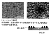
- FIG. 1 shows the SEM image of the crater occurrence location and the cause. As shown in FIG. 1, when inclusions such as cuprous oxide are present on the surface layer of the copper foil, the formation of roughened particles is hindered, and craters (processing hole “spots”) are generated in the portions.
- the present invention can solve the problems caused by the copper foil and the copper alloy foil by applying the base plating.
- the base plating is 0.15 ⁇ m or more, more preferably 0.2 ⁇ m or more.
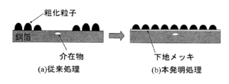
- Suitable conditions for base plating is good and the current density of 15.0A / dm 2 or more (41As / dm 2 or more coulombs). This is shown in FIG.
- the base plating layer covers inclusions such as cuprous oxide on the surface of the copper foil, the subsequent roughening process is performed smoothly, and the generation of craters is eliminated.
- a heat-resistant layer of Co—Ni may be provided, and a chromate layer may be provided as a rust preventive layer.
- a typical heat-resistant layer adhesion amount is a Co—Ni layer (Co: 200 to 3,000 ⁇ g / dm 2 , Ni: 100 to 2,000 ⁇ g / dm 2 ).
- the rolled copper or copper alloy foil roughened by the copper fine particles of the present invention is a rolled copper in which a copper base plating layer is formed between the copper roughened layer and the rolled copper or rolled copper alloy foil. Or it is copper alloy foil.
- the copper base plating layer preferably has a thickness of 0.15 ⁇ m or more and 0.30 ⁇ m or less. By forming this copper base plating layer in this way, it is possible to prevent the occurrence of craters in the roughened copper foil having copper fine particles of 0.25 ⁇ m or more and 0.45 ⁇ m or less.
- the roughened layer of the rolled copper or copper alloy foil has a Cu—Co—Ni of 0.05 ⁇ m or more and 0.25 ⁇ m or less on the copper roughened layer roughened by the copper fine particles.
- a roughening treatment layer composed of a fine particle layer of particles.
- the composition of the Cu—Co—Ni particles is Cu: 10 to 30 mg / dm 2 , Co: 100 to 3,000 ⁇ g / dm 2 , Ni: 50 to 500 ⁇ g / dm 2 , and this roughened layer
- This structure is a two-stage structure of a copper roughening layer roughened with copper fine particles and a Co—Ni—Cu particle fine particle layer. The occurrence of craters can also be prevented in rolled copper or copper alloy foil provided with this roughened layer.
- the copper roughened particle layer on the rolled copper foil is composed of copper sulfate (Cu conversion: 3 to 50 g / L), sulfuric acid: 1 to 150 g / L, temperature: 20 to 40 ° C., Dk: 30 to 70 A / dm. It is formed by roughening plating under the condition of 2 .
- crater a crater-like defect (referred to as “crater” in the present specification) occurred even in a pure copper-based rolled copper foil, and particularly when a rolled copper alloy foil was used.
- This roughened rolled copper or copper alloy foil crater (defect) is also observed with an optical microscope, and the crater (defect spot) is clearer in the SEM image of FIG. A defect spot is seen at the tip).
- the number of craters tends to increase as the current density increases.
- the crater is a processing hole (spot).
- copper particles are not formed or are diluted.
- the reason why this crater occurs is not necessarily technically elucidated.
- the generation of craters is considered to be caused by the difference in concentration or segregation of impurities contained in copper or copper alloy or components of copper alloy foil.
- Such craters are about 15 to 70 pieces / 25 mm 2 .
- This crater forms a clear shadow or black spot on a gold plating layer or the like to be subsequently processed, and the appearance is remarkably impaired.
- a copper base plating layer is formed between the copper roughening layer and the rolled copper or rolled copper alloy foil.
- the condition of the base plating is copper sulfate (Cu conversion: 15 to 25 g / L). ), Sulfuric acid: 80 to 120 g / L, temperature: 40 to 60 ° C., Dk: 15 to 20 A / dm 2 .
- the roughening of the rolled copper or copper alloy foil of the present invention includes copper sulfate (Cu conversion: 3 to 50 g / L), nickel sulfate (Ni conversion: 1 to 50 g / L, preferably 1 to 3 g / L), Conditions of phosphoric acid (P conversion: 0.75 to 1000 g / L, preferably 0.75 to 1 g / L), sulfuric acid: 1 to 150 g / L, temperature: 20 to 40 ° C., Dk: 30 to 70 A / dm 2
- Cu conversion 3 to 50 g / L
- Ni conversion 1 to 50 g / L, preferably 1 to 3 g / L
- Conditions of phosphoric acid P conversion: 0.75 to 1000 g / L, preferably 0.75 to 1 g / L
- sulfuric acid 1 to 150 g / L
- temperature 20 to 40 ° C.
- Dk 30 to 70 A / dm 2
- the number of craters existing on the roughened surface of the rolled copper alloy foil roughened by the copper fine particles can be reduced to 0.5 pieces / mm 2 or less.
- normal peel strength, surface roughness, and glossiness are all good, and it has high strength, which is a property unique to rolled copper foil, and is further subjected to roughening rolling by a conventional copper fine particle layer. It has excellent properties such as acid resistance, tin plating solution resistance, and adhesive strength with resin equivalent to copper foil.
- the pure copper-based rolled copper foil oxygen-free copper or tough pitch copper (containing 0.02 to 0.05% oxygen) can be used.
- the copper alloy foil is not particularly limited, and the present invention can be applied as long as craters are generated due to concentration differences or segregation of components of the copper alloy foil.
- a copper alloy consisting of 0.05 to 1 wt% Cr, 0.05 to 1 wt% Zr, 0.05 to 1 wt% Zn, the balance Cu and inevitable impurities, or 1 to 5 wt% Ni, 0.1 to 3 wt% Si , 0.05 to 3 wt% Mg, the remainder Cu and inevitable impurities are desirably applied to the copper alloy foil.
- the produced rolled copper foil is continuously wound around a coil, but the copper foil obtained as described above is further subjected to surface treatment or coating treatment (coating) such as electrochemical or chemical or resin. It can be used for printed wiring boards.
- the copper foil is required to have a thickness of 18 ⁇ m or less, more preferably 3 to 12 ⁇ m in order to be used as a high-density wiring.
- the roughened rolled copper or copper alloy foil of the present invention is Such a thickness can be applied without limitation, and can also be applied to an ultrathin foil or a thick copper foil. Further, as other surface treatments, chromium-based metal, zinc-based metal, and organic rust preventive treatment can be performed as necessary. In addition, a coupling treatment such as silane can be performed. These are suitably selected according to the use of the copper foil of a printed wiring board, and this invention includes all these.
- a rolled copper foil having a surface roughness of 2.5 ⁇ m or less and not roughened is used as the rolled copper or copper alloy foil. It is as follows when the specific example of the copper roughening plating processing liquid containing the nickel metal or phosphorus of this invention formed in these rolled copper or copper alloy foil is shown.
- Example 1 As the copper foil, a rolled copper alloy foil made of Cr: 0.2 wt%, Zr: 0.1 wt%, Zn: 0.2 wt%, the remainder Cu and inevitable impurities was used. This rolled copper foil is degreased and washed with water, followed by pickling and washing, followed by copper sulfate (Cu conversion: 20 g / L), sulfuric acid: 100 g / L, temperature: 50 ° C., Dk: 5.0 A / dm. 2 (C: 10.3 As / dm 2 ) A 0.04 ⁇ m thick copper base plating layer was formed. The thickness of the base plating layer is a trial calculation value from the coulomb amount and the copper specific gravity.
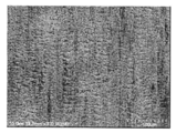
- FIG. 4 shows an SEM image of the surface of the rolled copper foil of this example after the base plating and then the copper roughening treatment. Thus, no craters were observed on many surfaces.
- the number of craters was determined by counting the number of craters on the roughened copper surface with an optical microscope when the thickness of the underlying plating was variously changed. As is clear from Table 1, in this example, the generation of craters was small, and the number was 4.2 / 25 mm 2 .
- Example 2 The copper base plating layer was formed under the conditions of Dk: 10.0 A / dm 2 (C: 20.7 As / dm 2 ), and a 0.08 ⁇ m thick copper base plating layer was formed. Other conditions are the same as in the first embodiment.
- the number of craters on the roughened copper surface was counted with an optical microscope, and the number was examined. The results are similarly shown in Table 1 above. As shown in Table 1, the occurrence of craters in Example 2 was small, and the number was 2.1 / 25 mm 2 .
- Example 3 The copper base plating layer was formed under the conditions of Dk: 15.0 A / dm 2 (C: 41.0 As / dm 2 ), and a copper base plating layer having a thickness of 0.15 ⁇ m was formed. Other conditions are the same as in the first embodiment.
- the number of craters on the roughened copper surface was counted with an optical microscope, and the number was examined. The results are similarly shown in Table 1 above. As shown in Table 1, the occurrence of craters in Example 3 was small, and the number of craters was 0.5 / 25 mm 2 .
- Example 4 The formation condition of the copper base plating layer was Dk: 17.5 A / dm 2 (C: 67.2 As / dm 2 ), and a copper base plating layer having a thickness of 0.25 ⁇ m was formed. Other conditions are the same as in the first embodiment.
- the number of craters on the roughened copper surface was counted with an optical microscope, and the number was examined. The results are similarly shown in Table 1 above. As shown in Table 1, the occurrence of craters in Example 4 was small, which was 0.0 pieces / 25 mm 2 .
- Example 5 The formation condition of the copper base plating layer was a condition of Dk: 20.0 A / dm 2 (C: 72.4 As / dm 2 ), and a copper base plating layer having a thickness of 0.27 ⁇ m was formed. Other conditions are the same as in the first embodiment.
- the number of craters on the roughened copper surface was counted with an optical microscope, and the number was examined. The results are similarly shown in Table 1 above. As shown in Table 1, the occurrence of craters in Example 5 was small, and the number was 0.0 pieces / 25 mm 2 .
- Comparative Example 1 In this comparative example 1, it was a case where there was no base plating, and other conditions were the same as those of the example 1. As a result, the number of craters was 10.0 / 25 mm 2 , which was very large. The results are also shown in Table 1.
- the present invention can provide a roughened rolled copper alloy foil with reduced craters, which is a significant drawback peculiar to a rolled copper alloy foil having a roughened surface, and is particularly present in the surface layer of the base material or in the vicinity thereof. It has an excellent effect of suppressing the occurrence of craters caused by inclusions. In addition, it has high strength, adhesive strength with the resin layer, acid resistance and tin plating solution resistance, high peel strength, and good etching properties and glossiness. This is extremely effective for the production of a flexible printed circuit board or the like capable of making a fine pattern of the roughened rolled copper alloy foil wiring of the present invention.
Landscapes
- Chemical & Material Sciences (AREA)
- Engineering & Computer Science (AREA)
- Chemical Kinetics & Catalysis (AREA)
- Electrochemistry (AREA)
- Materials Engineering (AREA)
- Metallurgy (AREA)
- Organic Chemistry (AREA)
- Microelectronics & Electronic Packaging (AREA)
- Crystallography & Structural Chemistry (AREA)
- Manufacturing & Machinery (AREA)
- Electroplating Methods And Accessories (AREA)
- Parts Printed On Printed Circuit Boards (AREA)
Abstract
Description
従来、粗化処理し樹脂との接着性を向上させた電解銅箔が使用されていたが、この粗化処理のために銅箔のエッチング性が著しく損なわれ、高アスペクト比でのエッチングが困難となり、エッチング時にアンダーカットが発生し、十分なファインパターン化ができないという問題が生じた。
しかしながら、電解銅箔のロープロファイル化は電解銅箔と絶縁性のポリイミド層との間の密着強度を低下させるという問題がある。このためハイレベルなファインパターン化の要求はあるが、一方では所期の接着強度を維持することができず、配線がポリイミド層から加工段階で剥離してしまうなどの問題が発生した。
また、アンダーカットを防止する目的で、電解銅箔上にリン含有ニッケルめっき層を形成する技術が提案されている(例えば、特許文献2参照)。しかし、この場合の電解銅箔の面は、粗面であることを要件としており、少なくともそれを許容している技術である。また、特許文献2の実施例は全て、電解銅箔の粗面にリン含有ニッケルめっき層を形成するものである。
しかし、従来はこのような総合的な問題が検討されているとは言えず、上記の問題を解決できる好適な銅箔が見出されていないのが現状である。
一般に、通常の純銅系の圧延銅箔に、さらに微細な銅めっき(通称「赤処理」)を施し、樹脂等との密着強度を向上させた銅箔は公知である。
通常、この粗化処理面の上にさらに、銅とコバルトの合金めっき又は銅、コバルト、ニッケルの3元合金をめっきして印刷回路用の銅箔に供せられている(特許文献3及び特許文献4参照)。
ところが、このような銅合金圧延銅箔に銅をめっきし、微細な銅粒子を形成した場合、クレータと呼ばれる欠陥が発生した。このクレータは処理の抜け穴(スポット)となったもので、換言すれば銅粒子が形成されていない又は希薄となった無処理欠陥である。 なお、このクレータの面積は、約10~50μm2、平均直径3~10μm程度である。本願明細書で用いるクレータは、この意味で使用する。
また、圧延銅合金箔においては、添加元素が酸化し易い元素、例えば、Zrを含有する場合には、これらの酸化物が該当する。また、硫化物の例としては、硫化銅である。
そして、クレータは銅をベースとする粗化処理について発生しやすい。クレータの発生箇所のSEM画像とその原因を、図1に示す。
この図1に示すように、銅箔の表層に亜酸化銅などの介在物があると、粗化粒子の形成が阻害され、その部分にクレータ(処理の抜け穴「スポット」)が発生する。
下地めっきの好適な条件としては、電流密度を15.0A/dm2以上(クーロン量で41As/dm2以上)とするのが良い。この様子を、図2に示す。
この図2に示すように、下地めっき層が銅箔の表層の亜酸化銅などの介在物を覆うようになるので、その後の粗化処理が円滑に行われ、クレータの発生がなくなる。
粗化処理の後は、Co-Niの耐熱層を設けてよく、防錆層としてクロメート層を施しても良い。代表的な耐熱層の付着量としては、Co-Ni層(Co:200~3,000μg/dm2、Ni:100~2,000μg/dm2)である。
このようにこの銅下地めっき層を形成することで、0.25μm以上、0.45μm以下の銅微細粒子を有する粗化処理された銅箔について、クレータの発生を防止することができる。
この粗化処理層を備えた圧延銅又は銅合金箔圧延銅又は銅合金箔にも、クレータの発生を防止することができる。
しかし、圧延銅又は圧延合金箔特有の現象であることから、クレータの発生は銅又は銅合金に含有される不純物又は銅合金箔の成分の濃度差又は偏析に起因するものと考えられる。このようなクレータは、15~70個/25mm2程度になる。このクレータは、その後に処理される金めっき層等に明瞭な影又は黒点を形成し、外観を著しく損ねる。
また、本発明の圧延銅又は銅合金箔の粗化は、硫酸銅(Cu換算:3~50g/L)、硫酸ニッケル(Ni換算:1~50g/L、好ましくは1~3g/L)、燐酸(P換算:0.75~1000g/L、好ましくは0.75~1g/L)、硫酸:1~150g/L、温度:20~40°C、Dk:30~70A/dm2の条件で粗化めっきすることによって行なう。銅微細粒子は通常0.1~2.0μmの範囲に形成する。
下記実施例に示すように、常態ピール強度、表面粗さ、光沢度はいずれも良好であり、また圧延銅箔固有の性質である高強度を備え、さらに従来の銅微粒子層による粗化処理圧延銅箔と同等の耐酸性、耐錫めっき液性及び樹脂との接着強度を有するという優れた特性を有する。
製造された圧延銅箔は連続的にコイルに巻かれるが、上記のようにして得た銅箔は、その後さらに電気化学的若しくは化学的又は樹脂等の表面処理又は被覆処理(コーティング)を施してプリント配線板等に使用することができる。
これらの圧延銅又は銅合金箔に形成する本発明のニッケル金属又はリンを含有する銅粗化めっき処理液の具体例を示すと、次の通りである。
(銅-ニッケル-リン合金めっき処理)
Cuイオン濃度:3~50g/L
Niイオン濃度:1~50g/L
Pイオン濃度:0.75~1000g/L
硫酸:1~150g/L
電解液温度:20~40°C、
pH:2.0~4.0
電流密度:30~70A/dm2、
電着換算厚み0.3~25nm
銅箔として、Cr:0.2wt%、Zr:0.1wt%、Zn:0.2wt%、残部Cu及び不可避不純物からなる圧延銅合金箔を使用した。
この圧延銅箔を、脱脂及び水洗処理、続いて酸洗・水洗処理した後、硫酸銅(Cu換算:20g/L)、硫酸:100g/L、温度:50℃、Dk:5.0A/dm2(C:10.3As/dm2)の条件で、0.04μm厚の銅の下地めっき層を形成した。下地めっき層の厚みは、クーロン量と銅比重からの試算値である。
この粗化めっきした圧延銅合金箔について、下記に示す条件で各種の評価試験を実施した。なお、本発明との対比のために、比較例を掲載した。この比較例については、無添加の場合の、銅粗化処理を施したものである。これらの結果を、表1に示す。
本実施例の圧延銅箔に下地めっき施した後、銅粗化処理した表面のSEM画像を図4に示す。このように、多くの表面でクレータは観察されなかった。
クレータの個数は、下地めっき厚みを種々変化させた場合の、銅粗化面のクレータ数を光学顕微鏡によりカウントし、その個数を調べた。
表1から明らかなように、本実施例はクレータの発生が少なく、4.2個/25mm2となった。

銅の下地めっき層の形成条件を、Dk:10.0A/dm2(C:20.7As/dm2)の条件で、0.08μm厚の銅の下地めっき層を形成した。他の条件は、実施例1と同様である。銅粗化面のクレータ数を光学顕微鏡によりカウントし、その個数を調べた。この結果を、同様に上記表1に示す。表1に示すように、本実施例2のクレータの発生が少なく、2.1個/25mm2となった。
銅の下地めっき層の形成条件を、Dk:15.0A/dm2(C:41.0As/dm2)の条件で、0.15μm厚の銅の下地めっき層を形成した。他の条件は、実施例1と同様である。銅粗化面のクレータ数を光学顕微鏡によりカウントし、その個数を調べた。この結果を、同様に上記表1に示す。表1に示すように、本実施例3のクレータの発生が少なく、0.5個/25mm2となった。
銅の下地めっき層の形成条件を、Dk:17.5A/dm2(C:67.2As/dm2)の条件で、0.25μm厚の銅の下地めっき層を形成した。他の条件は、実施例1と同様である。銅粗化面のクレータ数を光学顕微鏡によりカウントし、その個数を調べた。この結果を、同様に上記表1に示す。表1に示すように、本実施例4のクレータの発生が少なく、0.0個/25mm2となった。
銅の下地めっき層の形成条件を、Dk:20.0A/dm2(C:72.4As/dm2)の条件で、0.27μm厚の銅の下地めっき層を形成した。他の条件は、実施例1と同様である。銅粗化面のクレータ数を光学顕微鏡によりカウントし、その個数を調べた。この結果を同様に、上記表1に示す。表1に示すように、本実施例5のクレータの発生が少なく、0.0個/25mm2となった。
この比較例1では、下地めっき無しの場合であり、他の条件は、実施例1と同様の条件とした。この結果、クレータ数が10.0個/25mm2となり、極めて多いという結果になった。この結果も、同様に表1に示す。
Claims (5)
- 銅微細粒子により粗化処理された圧延銅又は銅合金箔であって、該銅粗化処理層と圧延銅又は圧延銅合金箔との間に、銅の下地めっき層を備えていることを特徴とする粗化処理面を備えた圧延銅又は銅合金箔。
- 前記銅下地めっき層の厚みが0.15μm以上、0.30μm以下であることを特徴とする請求項1記載の粗化処理面を備えた圧延銅又は銅合金箔。
- 前記銅微細粒子により粗化処理された銅粗化処理層が0.25μm以上、0.45μm以下の銅微細粒子であることを特徴とする請求項1又は2記載の圧延銅又は銅合金箔。
- 前記銅微細粒子により粗化処理された銅粗化処理層の上に、さらに0.05μm以上、0.25μm以下のCo-Ni-Cu粒子の微細粒子からなる粗化処理層を備えていることを特徴とする請求項1~3のいずれか一項に記載の圧延銅又は銅合金箔。
- Co-Ni-Cu粒子の組成が、Cu:10~30mg/dm2、Ni:50~500μg/dm2、Co:100~3,000μg/dm2であることを特徴とする請求項4に記載の圧延銅又は銅合金箔。
Priority Applications (5)
| Application Number | Priority Date | Filing Date | Title |
|---|---|---|---|
| US14/004,794 US9049795B2 (en) | 2011-03-25 | 2012-02-10 | Rolled copper or copper-alloy foil provided with roughened surface |
| JP2013507241A JPWO2012132576A1 (ja) | 2011-03-25 | 2012-02-10 | 粗化処理面を備えた圧延銅又は銅合金箔 |
| KR1020137024129A KR20130124383A (ko) | 2011-03-25 | 2012-02-10 | 조화 처리면을 구비한 압연 구리 또는 구리 합금박 |
| CN201280015153.2A CN103459679B (zh) | 2011-03-25 | 2012-02-10 | 具备粗化处理面的压延铜或铜合金箔 |
| PH1/2013/501979A PH12013501979A1 (en) | 2011-03-25 | 2012-10-02 | Rolled copper or copper-alloy foil provided with roughened surface |
Applications Claiming Priority (2)
| Application Number | Priority Date | Filing Date | Title |
|---|---|---|---|
| JP2011-067748 | 2011-03-25 | ||
| JP2011067748 | 2011-03-25 |
Publications (1)
| Publication Number | Publication Date |
|---|---|
| WO2012132576A1 true WO2012132576A1 (ja) | 2012-10-04 |
Family
ID=46930340
Family Applications (1)
| Application Number | Title | Priority Date | Filing Date |
|---|---|---|---|
| PCT/JP2012/053106 Ceased WO2012132576A1 (ja) | 2011-03-25 | 2012-02-10 | 粗化処理面を備えた圧延銅又は銅合金箔 |
Country Status (8)
| Country | Link |
|---|---|
| US (1) | US9049795B2 (ja) |
| JP (1) | JPWO2012132576A1 (ja) |
| KR (1) | KR20130124383A (ja) |
| CN (1) | CN103459679B (ja) |
| MY (1) | MY164997A (ja) |
| PH (1) | PH12013501979A1 (ja) |
| TW (1) | TWI530591B (ja) |
| WO (1) | WO2012132576A1 (ja) |
Families Citing this family (4)
| Publication number | Priority date | Publication date | Assignee | Title |
|---|---|---|---|---|
| WO2011138876A1 (ja) | 2010-05-07 | 2011-11-10 | Jx日鉱日石金属株式会社 | 印刷回路用銅箔 |
| PH12013500540B1 (en) | 2010-09-27 | 2020-02-14 | Jx Nippon Mining & Metals Corp | Copper foil for printed wiring board, method for producing said copper foil, resin substrate for printed wiring board, and printed wiring board |
| CN104735929B (zh) * | 2013-12-24 | 2017-12-29 | 深南电路有限公司 | 电路板加工方法和设备 |
| CN110962280B (zh) * | 2018-09-28 | 2021-09-03 | 比亚迪股份有限公司 | 金属树脂复合体及其制备方法和电子产品外壳 |
Citations (4)
| Publication number | Priority date | Publication date | Assignee | Title |
|---|---|---|---|---|
| JP2002241989A (ja) * | 2000-11-27 | 2002-08-28 | Furukawa Circuit Foil Kk | 金属複合体シート、それを用いた回路基板用の積層板 |
| JP2009164488A (ja) * | 2008-01-09 | 2009-07-23 | Hitachi Cable Ltd | プリント配線板用銅箔 |
| JP2010037585A (ja) * | 2008-08-01 | 2010-02-18 | Hitachi Cable Ltd | 銅箔及び銅箔製造方法 |
| WO2011138876A1 (ja) * | 2010-05-07 | 2011-11-10 | Jx日鉱日石金属株式会社 | 印刷回路用銅箔 |
Family Cites Families (23)
| Publication number | Priority date | Publication date | Assignee | Title |
|---|---|---|---|---|
| US4159231A (en) * | 1978-08-04 | 1979-06-26 | The United States Of America As Represented By The Secretary Of The Interior | Method of producing a lead dioxide coated cathode |
| JPS56155592A (en) | 1980-04-03 | 1981-12-01 | Furukawa Circuit Foil | Copper foil for printed circuit and method of manufacturing same |
| EP0396056B1 (en) * | 1989-05-02 | 1994-01-05 | Nikko Gould Foil Co., Ltd. | Treatment of copper foil for printed circuits |
| JPH0650794B2 (ja) | 1989-05-02 | 1994-06-29 | 日鉱グールド・フォイル株式会社 | 印刷回路用銅箔の処理方法 |
| JPH0650795B2 (ja) | 1989-05-02 | 1994-06-29 | 日鉱グールド・フォイル株式会社 | 印刷回路用銅箔の処理方法 |
| EP0695377B1 (en) * | 1993-04-19 | 2001-06-27 | GA-TEK Inc. | Process for making copper metal powder, copper oxides and copper foil |
| JP2849059B2 (ja) | 1995-09-28 | 1999-01-20 | 日鉱グールド・フォイル株式会社 | 印刷回路用銅箔の処理方法 |
| JP3258308B2 (ja) | 2000-02-03 | 2002-02-18 | 株式会社日鉱マテリアルズ | レーザー穴開け性に優れた銅箔及びその製造方法 |
| US20020182432A1 (en) | 2000-04-05 | 2002-12-05 | Masaru Sakamoto | Laser hole drilling copper foil |
| JP3768104B2 (ja) | 2001-01-22 | 2006-04-19 | ソニーケミカル株式会社 | フレキシブルプリント基板 |
| JP4298943B2 (ja) | 2001-10-18 | 2009-07-22 | 日鉱金属株式会社 | 銅箔表面処理剤 |
| JP4379854B2 (ja) | 2001-10-30 | 2009-12-09 | 日鉱金属株式会社 | 表面処理銅箔 |
| JP4316413B2 (ja) | 2004-04-05 | 2009-08-19 | 日鉱金属株式会社 | 粗化処理面を備えた銅合金箔及び銅合金箔の粗化処理方法 |
| CN101466875B (zh) | 2006-06-12 | 2011-01-05 | 日矿金属株式会社 | 具有粗化处理面的轧制铜或铜合金箔以及该轧制铜或铜合金箔的粗化方法 |
| JP5512273B2 (ja) | 2007-09-28 | 2014-06-04 | Jx日鉱日石金属株式会社 | 印刷回路用銅箔及び銅張積層板 |
| WO2009154066A1 (ja) | 2008-06-17 | 2009-12-23 | 日鉱金属株式会社 | 印刷回路基板用銅箔及び印刷回路基板用銅張積層板 |
| MY150825A (en) | 2008-11-25 | 2014-02-28 | Jx Nippon Mining & Metals Corp | Copper foil for printed circuit |
| CN107263959A (zh) | 2009-06-05 | 2017-10-20 | 吉坤日矿日石金属株式会社 | 半导体封装基板用铜箔及半导体封装用基板 |
| WO2010147013A1 (ja) | 2009-06-19 | 2010-12-23 | Jx日鉱日石金属株式会社 | 銅箔及びその製造方法 |
| MY172093A (en) | 2009-12-24 | 2019-11-13 | Jx Nippon Mining & Metals Corp | Surface-treated copper foil |
| JP5417458B2 (ja) | 2010-01-25 | 2014-02-12 | Jx日鉱日石金属株式会社 | 二次電池負極集電体用銅箔 |
| US20130189538A1 (en) | 2010-09-24 | 2013-07-25 | Jx Nippon Mining & Metals Corporation | Method of manufacturing copper foil for printed wiring board, and copper foil printed wiring board |
| PH12013500540B1 (en) | 2010-09-27 | 2020-02-14 | Jx Nippon Mining & Metals Corp | Copper foil for printed wiring board, method for producing said copper foil, resin substrate for printed wiring board, and printed wiring board |
-
2012
- 2012-02-10 KR KR1020137024129A patent/KR20130124383A/ko not_active Ceased
- 2012-02-10 JP JP2013507241A patent/JPWO2012132576A1/ja active Pending
- 2012-02-10 CN CN201280015153.2A patent/CN103459679B/zh active Active
- 2012-02-10 WO PCT/JP2012/053106 patent/WO2012132576A1/ja not_active Ceased
- 2012-02-10 US US14/004,794 patent/US9049795B2/en active Active
- 2012-02-10 MY MYPI2013003430A patent/MY164997A/en unknown
- 2012-02-15 TW TW101104869A patent/TWI530591B/zh active
- 2012-10-02 PH PH1/2013/501979A patent/PH12013501979A1/en unknown
Patent Citations (4)
| Publication number | Priority date | Publication date | Assignee | Title |
|---|---|---|---|---|
| JP2002241989A (ja) * | 2000-11-27 | 2002-08-28 | Furukawa Circuit Foil Kk | 金属複合体シート、それを用いた回路基板用の積層板 |
| JP2009164488A (ja) * | 2008-01-09 | 2009-07-23 | Hitachi Cable Ltd | プリント配線板用銅箔 |
| JP2010037585A (ja) * | 2008-08-01 | 2010-02-18 | Hitachi Cable Ltd | 銅箔及び銅箔製造方法 |
| WO2011138876A1 (ja) * | 2010-05-07 | 2011-11-10 | Jx日鉱日石金属株式会社 | 印刷回路用銅箔 |
Also Published As
| Publication number | Publication date |
|---|---|
| CN103459679A (zh) | 2013-12-18 |
| JPWO2012132576A1 (ja) | 2014-07-24 |
| TWI530591B (zh) | 2016-04-21 |
| PH12013501979A1 (en) | 2013-11-25 |
| CN103459679B (zh) | 2016-06-15 |
| US9049795B2 (en) | 2015-06-02 |
| KR20130124383A (ko) | 2013-11-13 |
| TW201245499A (en) | 2012-11-16 |
| MY164997A (en) | 2018-02-28 |
| US20140037976A1 (en) | 2014-02-06 |
Similar Documents
| Publication | Publication Date | Title |
|---|---|---|
| JP4890546B2 (ja) | 粗化処理面を備えた圧延銅又は銅合金箔及び圧延銅又は銅合金箔の粗化方法 | |
| JP5654581B2 (ja) | 印刷回路用銅箔、銅張積層板、印刷回路基板、印刷回路及び電子機器 | |
| JP5318886B2 (ja) | 印刷回路用銅箔 | |
| JP5399489B2 (ja) | 銅箔及びその製造方法 | |
| US9060431B2 (en) | Liquid crystal polymer copper-clad laminate and copper foil used for said laminate | |
| JP2005048269A (ja) | 表面処理銅箔およびそれを使用した基板 | |
| JP5913356B2 (ja) | 印刷回路用銅箔 | |
| JP6205269B2 (ja) | 印刷回路用銅箔、銅張積層板、プリント配線板、印刷回路板及び電子機器 | |
| TWI530591B (zh) | Rolled copper or copper alloy foil with roughened surface | |
| WO2013065831A1 (ja) | 印刷回路用銅箔 | |
| JP5738964B2 (ja) | 電子回路及びその形成方法並びに電子回路形成用銅張積層板 | |
| JP4316413B2 (ja) | 粗化処理面を備えた銅合金箔及び銅合金箔の粗化処理方法 | |
| JP2016188431A (ja) | 印刷回路用銅箔 |
Legal Events
| Date | Code | Title | Description |
|---|---|---|---|
| 121 | Ep: the epo has been informed by wipo that ep was designated in this application |
Ref document number: 12764412 Country of ref document: EP Kind code of ref document: A1 |
|
| DPE1 | Request for preliminary examination filed after expiration of 19th month from priority date (pct application filed from 20040101) | ||
| ENP | Entry into the national phase |
Ref document number: 2013507241 Country of ref document: JP Kind code of ref document: A |
|
| ENP | Entry into the national phase |
Ref document number: 20137024129 Country of ref document: KR Kind code of ref document: A |
|
| NENP | Non-entry into the national phase |
Ref country code: DE |
|
| WWE | Wipo information: entry into national phase |
Ref document number: 1301005371 Country of ref document: TH |
|
| WWE | Wipo information: entry into national phase |
Ref document number: 14004794 Country of ref document: US |
|
| 122 | Ep: pct application non-entry in european phase |
Ref document number: 12764412 Country of ref document: EP Kind code of ref document: A1 |