US9049795B2 - Rolled copper or copper-alloy foil provided with roughened surface - Google Patents
Rolled copper or copper-alloy foil provided with roughened surface Download PDFInfo
- Publication number
- US9049795B2 US9049795B2 US14/004,794 US201214004794A US9049795B2 US 9049795 B2 US9049795 B2 US 9049795B2 US 201214004794 A US201214004794 A US 201214004794A US 9049795 B2 US9049795 B2 US 9049795B2
- Authority
- US
- United States
- Prior art keywords
- copper
- alloy foil
- rolled
- roughened
- craters
- Prior art date
- Legal status (The legal status is an assumption and is not a legal conclusion. Google has not performed a legal analysis and makes no representation as to the accuracy of the status listed.)
- Active
Links
Images


Classifications
-
- H—ELECTRICITY
- H05—ELECTRIC TECHNIQUES NOT OTHERWISE PROVIDED FOR
- H05K—PRINTED CIRCUITS; CASINGS OR CONSTRUCTIONAL DETAILS OF ELECTRIC APPARATUS; MANUFACTURE OF ASSEMBLAGES OF ELECTRICAL COMPONENTS
- H05K1/00—Printed circuits
- H05K1/02—Details
- H05K1/09—Use of materials for the conductive, e.g. metallic pattern
-
- C—CHEMISTRY; METALLURGY
- C25—ELECTROLYTIC OR ELECTROPHORETIC PROCESSES; APPARATUS THEREFOR
- C25D—PROCESSES FOR THE ELECTROLYTIC OR ELECTROPHORETIC PRODUCTION OF COATINGS; ELECTROFORMING; APPARATUS THEREFOR
- C25D5/00—Electroplating characterised by the process; Pretreatment or after-treatment of workpieces
- C25D5/10—Electroplating with more than one layer of the same or of different metals
-
- C—CHEMISTRY; METALLURGY
- C25—ELECTROLYTIC OR ELECTROPHORETIC PROCESSES; APPARATUS THEREFOR
- C25D—PROCESSES FOR THE ELECTROLYTIC OR ELECTROPHORETIC PRODUCTION OF COATINGS; ELECTROFORMING; APPARATUS THEREFOR
- C25D5/00—Electroplating characterised by the process; Pretreatment or after-treatment of workpieces
- C25D5/60—Electroplating characterised by the structure or texture of the layers
- C25D5/605—Surface topography of the layers, e.g. rough, dendritic or nodular layers
-
- C—CHEMISTRY; METALLURGY
- C25—ELECTROLYTIC OR ELECTROPHORETIC PROCESSES; APPARATUS THEREFOR
- C25D—PROCESSES FOR THE ELECTROLYTIC OR ELECTROPHORETIC PRODUCTION OF COATINGS; ELECTROFORMING; APPARATUS THEREFOR
- C25D5/00—Electroplating characterised by the process; Pretreatment or after-treatment of workpieces
- C25D5/60—Electroplating characterised by the structure or texture of the layers
- C25D5/615—Microstructure of the layers, e.g. mixed structure
- C25D5/617—Crystalline layers
-
- C—CHEMISTRY; METALLURGY
- C25—ELECTROLYTIC OR ELECTROPHORETIC PROCESSES; APPARATUS THEREFOR
- C25D—PROCESSES FOR THE ELECTROLYTIC OR ELECTROPHORETIC PRODUCTION OF COATINGS; ELECTROFORMING; APPARATUS THEREFOR
- C25D7/00—Electroplating characterised by the article coated
- C25D7/06—Wires; Strips; Foils
- C25D7/0614—Strips or foils
-
- H—ELECTRICITY
- H05—ELECTRIC TECHNIQUES NOT OTHERWISE PROVIDED FOR
- H05K—PRINTED CIRCUITS; CASINGS OR CONSTRUCTIONAL DETAILS OF ELECTRIC APPARATUS; MANUFACTURE OF ASSEMBLAGES OF ELECTRICAL COMPONENTS
- H05K3/00—Apparatus or processes for manufacturing printed circuits
- H05K3/38—Improvement of the adhesion between the insulating substrate and the metal
- H05K3/382—Improvement of the adhesion between the insulating substrate and the metal by special treatment of the metal
- H05K3/384—Improvement of the adhesion between the insulating substrate and the metal by special treatment of the metal by plating
-
- C—CHEMISTRY; METALLURGY
- C25—ELECTROLYTIC OR ELECTROPHORETIC PROCESSES; APPARATUS THEREFOR
- C25D—PROCESSES FOR THE ELECTROLYTIC OR ELECTROPHORETIC PRODUCTION OF COATINGS; ELECTROFORMING; APPARATUS THEREFOR
- C25D3/00—Electroplating: Baths therefor
- C25D3/02—Electroplating: Baths therefor from solutions
- C25D3/38—Electroplating: Baths therefor from solutions of copper
-
- H—ELECTRICITY
- H05—ELECTRIC TECHNIQUES NOT OTHERWISE PROVIDED FOR
- H05K—PRINTED CIRCUITS; CASINGS OR CONSTRUCTIONAL DETAILS OF ELECTRIC APPARATUS; MANUFACTURE OF ASSEMBLAGES OF ELECTRICAL COMPONENTS
- H05K2201/00—Indexing scheme relating to printed circuits covered by H05K1/00
- H05K2201/03—Conductive materials
- H05K2201/0332—Structure of the conductor
- H05K2201/0335—Layered conductors or foils
- H05K2201/0355—Metal foils
-
- Y—GENERAL TAGGING OF NEW TECHNOLOGICAL DEVELOPMENTS; GENERAL TAGGING OF CROSS-SECTIONAL TECHNOLOGIES SPANNING OVER SEVERAL SECTIONS OF THE IPC; TECHNICAL SUBJECTS COVERED BY FORMER USPC CROSS-REFERENCE ART COLLECTIONS [XRACs] AND DIGESTS
- Y10—TECHNICAL SUBJECTS COVERED BY FORMER USPC
- Y10T—TECHNICAL SUBJECTS COVERED BY FORMER US CLASSIFICATION
- Y10T428/00—Stock material or miscellaneous articles
- Y10T428/12—All metal or with adjacent metals
- Y10T428/12014—All metal or with adjacent metals having metal particles
- Y10T428/12028—Composite; i.e., plural, adjacent, spatially distinct metal components [e.g., layers, etc.]
- Y10T428/12063—Nonparticulate metal component
- Y10T428/12069—Plural nonparticulate metal components
- Y10T428/12076—Next to each other
Definitions
- the present invention relates to a rolled copper or copper-alloy foil provided with a roughened surface.
- the present invention relates to a rolled copper or copper-alloy foil having fewer craters (which are failures in the roughening treatment caused by inclusions present at a surface layer of the copper foil), having good adhesive strength with a resin layer, having acid resistance and tin plating solution resistance, having high peel strength, having good etchability and glossiness, and suitable for manufacturing a flexible printed circuit board in which wiring can be finely patterned.
- a method comprising: forming a thin zinc-based metal layer on an electrolytic copper foil having a non-roughened surface; and further forming a polyimide-based resin layer thereon (for example, see Patent Document 1).
- Patent Document 2 proposes a technology in which a phosphorus-containing nickel plating layer is formed on an electrolytic copper foil in order to prevent undercutting.
- the surface of the electrolytic copper foil is required to be roughened or at least can be roughened.
- all of Examples in Patent Document 2 involve the formation of a phosphorus-containing nickel plating layer on a roughened surface of an electrolytic copper foil.
- problems are not limited to undercutting upon etching and adhesiveness with resin as described above. For example, strength, acid resistance, tin plating solution resistance, glossiness and the like are required to be excellent.
- a copper foil in which a common pure copper-based rolled copper foil is further subjected to fine copper plating (so-called “copper nodule treatment of red color”) to improve the adhesion strength with resin or the like.
- alloy plating of copper and cobalt or ternary alloy plating of copper, cobalt and nickel is further formed on this roughened surface to give a copper foil for printed circuits (see Patent Document 3 and Patent Document 4).
- a fault called a crater has occurred.
- This crater refers to a region of treatment failure (a spot), in other words, a non-treated fault in which copper grains are not formed or sparsely formed.
- the crater has an area of about 10 to 50 ⁇ m 2 and an average diameter of about 3 to 10 ⁇ m.
- the term “crater(s)” as used herein is used in this meaning.
- Patent Document 1 Japanese Patent Laid-Open No. 2002-217507
- Patent Document 2 Japanese Patent Laid-Open No. S56-155592
- Patent Document 3 Japanese Patent Publication No. H6-50794
- Patent Document 4 Japanese Patent Publication No. H6-50795
- Patent Document 5 Japanese Patent Laid-Open No. 2005-290521
- An object of the present invention is to provide a rolled copper or copper-alloy foil with a roughened surface having fewer craters, the presence of which is a serious disadvantage unique to a rolled copper-alloy foil having a roughened surface, and in particular, to provide a rolled copper or copper-alloy foil in which the development of craters caused by inclusions present in or near a surface layer of the base material can be reduced.
- a rolled copper or copper-alloy foil having high strength, good adhesive strength with a resin layer, acid resistance and tin plating solution resistance, and further having high peel strength, good etchability and glossiness, and suitable for a flexible printed circuit board in which wiring can be finely patterned.
- the present invention provides: 1) a rolled copper or copper-alloy foil provided with a roughened surface, the rolled copper or copper-alloy foil subjected to roughening treatment with copper fine grains wherein a copper base plating layer is provided between the copper roughened layer and the rolled copper or copper-alloy foil; 2) the rolled copper or copper-alloy foil provided with a roughened surface according to 1), wherein the copper base plating layer has a thickness of between 0.15 ⁇ m and 0.30 ⁇ m inclusive; and 3) the rolled copper or copper-alloy foil according to 1) or 2), wherein copper fine grains of the copper roughened layer obtained by roughening treatment with the copper fine gains have a size between 0.25 ⁇ m and 0.45 ⁇ m inclusive.
- the present invention provides: 4) the rolled copper or copper-alloy foil according to any one of 1) to 3), wherein a roughened layer comprising Co—Ni—Cu fine grains of between 0.05 ⁇ m and 0.25 ⁇ m inclusive is provided on the copper roughened layer obtained by roughening treatment with the fine copper grains; and 5) the rolled copper or copper-alloy foil according to 4), wherein the Co—Ni—Cu grains has a composition of Cu: 10 to 30 mg/dm 2 , Ni: 50 to 500 ⁇ g/dm 2 , and Co: 100 to 3,000 ⁇ g/dm 2 .
- the present invention enables to provide a roughened rolled copper-alloy foil having fewer craters (which are failures in the roughening treatment caused by inclusions present at a surface layer of the copper foil), the craters being a serious disadvantage unique to a rolled copper-alloy foil having a roughened surface.
- the present invention can inhibit the development of craters caused by inclusions present in or near a surface layer of the base material.
- the roughened rolled copper or copper-alloy foil has high strength, good adhesive strength with a resin layer, acid resistance, tin plating solution resistance, and high peel strength; shows good etchability and glossiness; and is suitable for manufacturing a flexible printed circuit board and the like in which wiring can be finely patterned.
- FIG. 1 This shows SEM images of the region where a crater is developed and the cause thereof.
- FIG. 2 This shows a method of reducing craters.
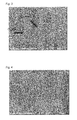
- FIG. 3 This shows a SEM image of a surface on which copper roughening treatment was performed without base plating on the rolled copper foil.
- FIG. 4 This shows a SEM image of a surface on which copper roughening treatment was performed after base plating on the rolled copper foil.
- inclusions used in the present invention refers to compound grains present in the matrix of a base material (a rolled copper foil or copper-alloy foil).
- they include oxides, sulfides, compounds between added elements, and the like.
- they are cupric oxide grains. In oxygen-free copper, there are very few cupric oxide grains, but there are considerable amount of oxides and sulfides from impurities.
- FIG. 1 shows SEM images of the region where a crater is developed and the cause thereof.
- the presence of inclusions such as cupric oxide in the surface of a copper foil inhibits the formation of roughening grains, resulting in the development of a crater (a region of treatment failure or “a spot”) at that region.
- the present invention can solve a fault resulting from a copper foil or a copper-alloy foil by providing base plating.
- Base plating is preferably 0.15 ⁇ m or more, more preferably 0.2 ⁇ m or more.
- base plating is thick, bending workability is decreased. Therefore too thick plating is not preferred, and specifically 0.3 ⁇ m or less is preferred.
- a current density of 15.0 A/dm 2 or more (41 As/dm 2 or more in the amount of coulomb) is preferred. This is shown in FIG. 2 .
- base plating is to cover inclusions such as cupric oxide in the surface of a copper foil, subsequent roughening treatment will be performed smoothly and the development of craters is inhibited.
- a heat resistant layer of Co—Ni may be provided, and/or a chromate layer may be provided as a rustproofing layer.
- a typical deposit amount of a heat resistant layer is Co: 200 to 3,000 ⁇ g/dm 2 , and Ni: 100 to 2,000 ⁇ g/dm 2 for a Co—Ni layer.
- the rolled copper or copper-alloy foil, which was subjected to roughening treatment with copper fine grains, of the present invention is a rolled copper or copper-alloy foil in which a copper base plating layer is formed between the copper roughened layer and the rolled copper or rolled copper-alloy foil.
- the copper base plating layer preferably has a thickness of between 0.15 ⁇ m and 0.30 ⁇ m inclusive.
- the development of craters can be prevented for a roughened copper foil having copper fine grains of between 0.25 ⁇ m and 0.45 ⁇ m inclusive.
- a fine-grain layer of Cu—Co—Ni grains of between 0.05 ⁇ m and 0.25 ⁇ m inclusive is provided, as a roughened layer, on the copper roughened layer obtained by roughening treatment with copper fine grains.
- the Cu—Co—Ni grains have a composition of Cu: 10 to 30 mg/dm 2 , Co: 100 to 3,000 ⁇ g/dm 2 , and Ni: 50 to 500 ⁇ g/dm 2 .
- the structure of this roughened layer will be a two-layered structure of: a copper roughened layer obtained by roughening treatment with copper fine grains; and a fine-grain layer of Co—Ni—Cu grains.
- the copper roughening grain layer on a rolled copper foil is formed by performing roughening plating under the conditions of copper sulfate (Cu equivalence: 3 to 50 g/L), sulfuric acid: 1 to 150 g/L, temperature: 20 to 40° C., and Dk: 30 to 70 A/dm 2 .
- craters crater-like defects
- These craters (defects) in the roughened rolled copper or copper-alloy foil can be observed even under a light microscope.
- the craters (defective spots) are more clearly observed in a SEM image in FIG. 3 (defective spots are seen at the tips of the arrows in FIG. 3 ).
- the number of craters tends to increase as the current density increases.
- craters are regions of treatment failure (spots) as described above. Copper grains are not formed or sparsely formed in the regions of the craters. The mechanism of the development of craters has not been necessarily elucidated technically.
- craters appear to be caused by impurities contained in a copper or copper alloy, or the difference in the concentration or segregation of the components in a copper-alloy foil since it is a phenomenon unique to a rolled copper or rolled alloy foil. About 15 to 70 of such craters will be developed per 25 mm 2 . These craters form clear shadows or black spots in a gold plating layer and the like to be provided later, significantly spoiling the appearance.
- a copper base plating layer is formed between the copper roughened layer and the rolled copper or rolled copper-alloy foil.
- the conditions for the base plating are as follows: copper sulfate (Cu equivalence: 15 to 25 g/L), sulfuric acid: 80 to 120 g/L, temperature: 40 to 60° C., and Dk: 15 to 20 A/dm 2 .
- roughening of the rolled copper or copper-alloy foil of the present invention is performed by roughening plating under the following conditions: copper sulfate (Cu equivalence: 3 to 50 g/L), nickel sulfate (Ni equivalence: 1 to 50 g/L, preferably 1 to 3 g/L), phosphoric acid (P equivalence: 0.75 to 1000 g/L, preferably 0.75 to 1 g/L), sulfuric acid: 1 to 150 g/L, temperature: 20 to 40° C., and Dk: 30 to 70 A/dm 2 . Copper fine grains are usually formed in the range of 0.1 to 2.0 ⁇ m.
- the number of craters present in the roughened surface of a rolled copper-alloy foil subjected to roughening treatment with copper fine grains can be controlled to be 0.5/mm 2 or less.
- peel strength as received, surface roughness and glossiness are all good; and high strength which is unique to a rolled copper foil is maintained; and further, excellent characteristics of acid resistance, tin plating solution resistance and adhesive strength with resin, similar to those of a roughened rolled copper foil having a conventional copper grain layer, are achieved.
- oxygen-free copper and tough pitch copper oxygen content: 0.02 to 0.05%) can be used.
- copper-alloy foils there is no particular limitation for copper-alloy foils.
- the present invention can be applied in any copper-alloy foils as long as they develop craters caused by the difference in the concentration or segregation of components in the copper-alloy foils.
- a copper alloy comprising 0.05 to 1 wt % of Cr, 0.05 to 1 wt % of Zr, 0.05 to 1 wt % of Zn, and the reminder being Cu and unavoidable impurities; or a copper-alloy foil comprising 1 to 5 wt % of Ni, 0.1 to 3 wt % of Si, 0.05 to 3 wt % of Mg, and the remainder being Cu and unavoidable impurities.
- a copper-alloy foil comprising 1 to 5 wt % of Ni, 0.1 to 3 wt % of Si, 0.05 to 3 wt % of Mg, and the remainder being Cu and unavoidable impurities.
- a rolled copper foil manufactured is to be continuously wound around a coil.
- the copper foil obtained as described above can be used for a printed wiring board and the like after further performing electrochemical or chemical or resin or other surface treatment or coating treatment.
- the thickness of a copper foil used for high density wiring needs to be 18 ⁇ m or less, more preferably 3 to 12 ⁇ m.
- the thickness is not limited to the above range, and ultra thin foils or thick copper foils can also be used.
- rustproofing treatment with chromium-based metal, zinc-based metal or organic system can be performed if desired.
- Coupling treatment with silane and the like can also be performed.
- a rolled copper foil without roughening treatment having a surface roughness of 2.5 ⁇ m or less will be used.
- Temperature of electrolytic solution 20 to 40° C.
- Thickness in electrodeposition equivalence 0.3 to 25 nm
- a rolled copper alloy foil comprising Cr: 0.2 wt %, Zr: 0.1 wt %, Zn: 0.2 wt %, and the remainder being Cu and unavoidable impurities was used as a copper foil.
- This rolled copper foil was degreased and then washed with water, and subsequently washed with acid and then water, and then a copper base plating layer having a thickness of 0.04 ⁇ m was formed under the following conditions: copper sulfate (Cu equivalence: 20 g/L), sulfuric acid: 100 g/L, temperature: 50° C., and Dk: 5.0 A/dm 2 (C: 10.3 As/dm 2 ).
- the thickness of a base plating layer is a theoretical value from the amount of coulomb and the specific gravity of copper.
- FIG. 4 shows a SEM image of a surface on which copper roughening was performed after base plating on the rolled copper foil of this Example. As shown in the figure, craters were not observed on many regions of the surface.
- the number of craters on the copper roughened surface was counted under a light microscope with the thickness of the base plating changed variously.
- this Example showed fewer craters, and the number was 4.2 per 25 mm 2 .
- a copper base plating layer with a thickness of 0.08 ⁇ m was formed under the condition for forming a copper base plating layer of Dk: 10.0 A/dm 2 (C: 20.7 As/dm 2 ).
- Other conditions are the same as in Example 1.
- the number of craters on the copper roughened surface was counted under a light microscope to investigate the number. The results are also shown in Table 1. As shown in Table 1, Example 2 showed fewer craters, and the number was 2.1 per 25 mm 2 .
- a copper base plating layer with a thickness of 0.15 ⁇ m was formed under the condition for forming a copper base plating layer of Dk: 15.0 A/dm 2 (C: 41.0 As/dm 2 ).
- Other conditions are the same as in Example 1.
- the number of craters on the copper roughened surface was counted under a light microscope to investigate the number. The results are also shown in Table 1. As shown in Table 1, Example 3 showed fewer craters, and the number was 0.5 per 25 mm 2 .
- a copper base plating layer with a thickness of 0.25 ⁇ m was formed under the condition for forming a copper base plating layer of Dk: 17.5 A/dm 2 (C: 67.2 As/dm 2 ).
- Other conditions are the same as in Example 1.
- the number of craters on the copper roughened surface was counted under a light microscope to investigate the number. The results are also shown in Table 1. As shown in Table 1, Example 4 showed fewer craters, and the number was 0.0 per 25 mm 2 .
- a copper base plating layer with a thickness of 0.27 ⁇ m was formed under the condition for forming a copper base plating layer of Dk: 20.0 A/dm 2 (C: 72.4 As/dm 2 ).
- Other conditions are the same as in Example 1.
- the number of craters on the copper roughened surface was counted under a light microscope to investigate the number. The results are also shown in Table 1. As shown in Table 1, Example 5 showed fewer craters, and the number was 0.0 per 25 mm 2 .
- the present invention can provide a roughened rolled copper-alloy foil having fewer craters, the presence of which is a serious disadvantage unique to a rolled copper-alloy foil having a roughened surface.
- the present invention can control the development of craters caused by inclusions present in or near a surface layer of the base material. Further, achieved are high strength, good adhesive strength with a resin layer, acid resistance and tin plating solution resistance as well as high peel strength and good etchability and glossiness. Accordingly, the present invention is extremely effective for manufacturing a flexible printed circuit board and the like in which wiring can be finely patterned on the roughened rolled copper-alloy foil of the present invention.
Abstract
Description
| TABLE 1 | ||||
| Conditions | ||||
| for forming | ||||
| Conditions for base plating | roughening grains | |||
| Dk | C | Plating thickness | Dk | C | Number of craters | ||
| A/dm2 | As/dm2 | (μm) | A/dm2 | As/dm2 | per 25 mm2 | ||
| Comparative | 0.0 | 0.0 | 0.00 | 50 | 70 | 10.0 |
| Example | ||||||
| Example 1 | 5.0 | 10.3 | 0.04 | 50 | 70 | 4.2 |
| Example 2 | 10.0 | 20.7 | 0.08 | 50 | 70 | 2.1 |
| Example 3 | 15.0 | 41.0 | 0.15 | 50 | 70 | 0.5 |
| Example 4 | 17.5 | 67.2 | 0.25 | 50 | 70 | 0.0 |
| Example 5 | 20.0 | 72.4 | 0.27 | 50 | 70 | 0.0 |
Claims (17)
Applications Claiming Priority (3)
| Application Number | Priority Date | Filing Date | Title |
|---|---|---|---|
| JP2011-067748 | 2011-03-25 | ||
| JP2011067748 | 2011-03-25 | ||
| PCT/JP2012/053106 WO2012132576A1 (en) | 2011-03-25 | 2012-02-10 | Rolled copper or copper-alloy foil provided with roughened surface |
Publications (2)
| Publication Number | Publication Date |
|---|---|
| US20140037976A1 US20140037976A1 (en) | 2014-02-06 |
| US9049795B2 true US9049795B2 (en) | 2015-06-02 |
Family
ID=46930340
Family Applications (1)
| Application Number | Title | Priority Date | Filing Date |
|---|---|---|---|
| US14/004,794 Active US9049795B2 (en) | 2011-03-25 | 2012-02-10 | Rolled copper or copper-alloy foil provided with roughened surface |
Country Status (7)
| Country | Link |
|---|---|
| US (1) | US9049795B2 (en) |
| JP (1) | JPWO2012132576A1 (en) |
| KR (1) | KR20130124383A (en) |
| CN (1) | CN103459679B (en) |
| MY (1) | MY164997A (en) |
| TW (1) | TWI530591B (en) |
| WO (1) | WO2012132576A1 (en) |
Families Citing this family (4)
| Publication number | Priority date | Publication date | Assignee | Title |
|---|---|---|---|---|
| CN102884228B (en) | 2010-05-07 | 2015-11-25 | 吉坤日矿日石金属株式会社 | Copper foil for printed circuit |
| WO2012043182A1 (en) | 2010-09-27 | 2012-04-05 | Jx日鉱日石金属株式会社 | Copper foil for printed wiring board, method for producing said copper foil, resin substrate for printed wiring board, and printed wiring board |
| CN104735929B (en) * | 2013-12-24 | 2017-12-29 | 深南电路有限公司 | Circuit board processing method and equipment |
| CN110962280B (en) * | 2018-09-28 | 2021-09-03 | 比亚迪股份有限公司 | Metal-resin composite, preparation method thereof and electronic product shell |
Citations (27)
| Publication number | Priority date | Publication date | Assignee | Title |
|---|---|---|---|---|
| US4159231A (en) * | 1978-08-04 | 1979-06-26 | The United States Of America As Represented By The Secretary Of The Interior | Method of producing a lead dioxide coated cathode |
| US4935310A (en) | 1980-04-03 | 1990-06-19 | Furukawa Circuit Foil Co., Ltd. | Copper foil for a printed circuit and a method for the production thereof |
| JPH02292894A (en) | 1989-05-02 | 1990-12-04 | Nikko Guurudo Fuoiru Kk | Treatment method for copper foil for printed circuit |
| JPH02292895A (en) | 1989-05-02 | 1990-12-04 | Nikko Guurudo Fuoiru Kk | Treatment method for copper foil for printed circuit |
| US5019222A (en) * | 1989-05-02 | 1991-05-28 | Nikko Gould Foil Co., Ltd. | Treatment of copper foil for printed circuits |
| US5458746A (en) * | 1993-04-19 | 1995-10-17 | Magma Copper Company | Process for making copper metal powder, copper oxides and copper foil |
| JPH0987889A (en) | 1995-09-28 | 1997-03-31 | Nikko Gould Foil Kk | Treatment of copper foil for printed circuit |
| JP2002241989A (en) | 2000-11-27 | 2002-08-28 | Furukawa Circuit Foil Kk | Metallic composite sheet and laminate for circuit board using the sheet |
| US20020182432A1 (en) | 2000-04-05 | 2002-12-05 | Masaru Sakamoto | Laser hole drilling copper foil |
| US6638642B2 (en) | 2000-02-03 | 2003-10-28 | Nikko Materials Company, Limited | Copper foil excellent in laser beam drilling performance and production method therefor |
| US20040209109A1 (en) | 2001-10-30 | 2004-10-21 | Katsuyuki Tsuchida | Surface-treated copper foil |
| US6835442B2 (en) | 2001-01-22 | 2004-12-28 | Sony Chemicals Corp. | Flexible printed wiring board |
| US6835241B2 (en) | 2001-10-18 | 2004-12-28 | Nikko Materials Co., Ltd. | Surface treatment for copper foil |
| JP2005290521A (en) | 2004-04-05 | 2005-10-20 | Nikko Materials Co Ltd | Copper alloy foil provided with roughening-treated face and roughening treatment method for copper alloy foil |
| US20090162685A1 (en) | 2006-06-12 | 2009-06-25 | Nippon Mining & Metals Co., Ltd. | Rolled Copper or Copper Alloy Foil with Roughened Surface and Method of Roughening Rolled Copper or Copper Alloy Foil |
| JP2009164488A (en) | 2008-01-09 | 2009-07-23 | Hitachi Cable Ltd | Copper foil for a printed wiring board |
| JP2010037585A (en) | 2008-08-01 | 2010-02-18 | Hitachi Cable Ltd | Copper foil and copper foil manufacturing method |
| US20100212941A1 (en) | 2007-09-28 | 2010-08-26 | Nippon Mining And Metals Co., Ltd. | Copper Foil for Printed Circuit and Copper-Clad Laminate |
| US20110262764A1 (en) | 2008-11-25 | 2011-10-27 | Jx Nippon Mining & Metals Corporation | Copper Foil for Printed Circuit |
| WO2011138876A1 (en) | 2010-05-07 | 2011-11-10 | Jx日鉱日石金属株式会社 | Copper foil for printed circuit |
| US8142905B2 (en) | 2008-06-17 | 2012-03-27 | Jx Nippon Mining & Metals Corporation | Copper foil for printed circuit board and copper clad laminate for printed circuit board |
| US20120107637A1 (en) | 2009-06-05 | 2012-05-03 | Jx Nippon Mining & Metals Corporation | Copper Foil for Semiconductor Package Substrate and Substrate for Semiconductor Package |
| US20120135266A1 (en) | 2009-06-19 | 2012-05-31 | Jx Nippon Mining & Metals Corporation | Copper Foil and Method for Producing Same |
| US20120276412A1 (en) | 2009-12-24 | 2012-11-01 | Jx Nippon Mining & Metals Corporation | Surface-Treated Copper Foil |
| US20130011734A1 (en) | 2010-01-25 | 2013-01-10 | Jx Nippon Mining & Metals Corporation | Copper foil for negative electrode current collector of secondary battery |
| US20130189538A1 (en) | 2010-09-24 | 2013-07-25 | Jx Nippon Mining & Metals Corporation | Method of manufacturing copper foil for printed wiring board, and copper foil printed wiring board |
| US20130220685A1 (en) | 2010-09-27 | 2013-08-29 | Jx Nippon Mining & Metals Corporation | Copper foil for printed wiring board, method for producing said copper foil, resin substrate for printed wiring board and printed wiring board |
-
2012
- 2012-02-10 MY MYPI2013003430A patent/MY164997A/en unknown
- 2012-02-10 WO PCT/JP2012/053106 patent/WO2012132576A1/en active Application Filing
- 2012-02-10 KR KR1020137024129A patent/KR20130124383A/en active Search and Examination
- 2012-02-10 JP JP2013507241A patent/JPWO2012132576A1/en active Pending
- 2012-02-10 CN CN201280015153.2A patent/CN103459679B/en active Active
- 2012-02-10 US US14/004,794 patent/US9049795B2/en active Active
- 2012-02-15 TW TW101104869A patent/TWI530591B/en active
Patent Citations (28)
| Publication number | Priority date | Publication date | Assignee | Title |
|---|---|---|---|---|
| US4159231A (en) * | 1978-08-04 | 1979-06-26 | The United States Of America As Represented By The Secretary Of The Interior | Method of producing a lead dioxide coated cathode |
| US4935310A (en) | 1980-04-03 | 1990-06-19 | Furukawa Circuit Foil Co., Ltd. | Copper foil for a printed circuit and a method for the production thereof |
| JPH02292894A (en) | 1989-05-02 | 1990-12-04 | Nikko Guurudo Fuoiru Kk | Treatment method for copper foil for printed circuit |
| JPH02292895A (en) | 1989-05-02 | 1990-12-04 | Nikko Guurudo Fuoiru Kk | Treatment method for copper foil for printed circuit |
| US5019222A (en) * | 1989-05-02 | 1991-05-28 | Nikko Gould Foil Co., Ltd. | Treatment of copper foil for printed circuits |
| US5458746A (en) * | 1993-04-19 | 1995-10-17 | Magma Copper Company | Process for making copper metal powder, copper oxides and copper foil |
| JPH0987889A (en) | 1995-09-28 | 1997-03-31 | Nikko Gould Foil Kk | Treatment of copper foil for printed circuit |
| US6638642B2 (en) | 2000-02-03 | 2003-10-28 | Nikko Materials Company, Limited | Copper foil excellent in laser beam drilling performance and production method therefor |
| US20020182432A1 (en) | 2000-04-05 | 2002-12-05 | Masaru Sakamoto | Laser hole drilling copper foil |
| JP2002241989A (en) | 2000-11-27 | 2002-08-28 | Furukawa Circuit Foil Kk | Metallic composite sheet and laminate for circuit board using the sheet |
| US6835442B2 (en) | 2001-01-22 | 2004-12-28 | Sony Chemicals Corp. | Flexible printed wiring board |
| US6835241B2 (en) | 2001-10-18 | 2004-12-28 | Nikko Materials Co., Ltd. | Surface treatment for copper foil |
| US20040209109A1 (en) | 2001-10-30 | 2004-10-21 | Katsuyuki Tsuchida | Surface-treated copper foil |
| JP2005290521A (en) | 2004-04-05 | 2005-10-20 | Nikko Materials Co Ltd | Copper alloy foil provided with roughening-treated face and roughening treatment method for copper alloy foil |
| US20090162685A1 (en) | 2006-06-12 | 2009-06-25 | Nippon Mining & Metals Co., Ltd. | Rolled Copper or Copper Alloy Foil with Roughened Surface and Method of Roughening Rolled Copper or Copper Alloy Foil |
| US20100212941A1 (en) | 2007-09-28 | 2010-08-26 | Nippon Mining And Metals Co., Ltd. | Copper Foil for Printed Circuit and Copper-Clad Laminate |
| JP2009164488A (en) | 2008-01-09 | 2009-07-23 | Hitachi Cable Ltd | Copper foil for a printed wiring board |
| US8142905B2 (en) | 2008-06-17 | 2012-03-27 | Jx Nippon Mining & Metals Corporation | Copper foil for printed circuit board and copper clad laminate for printed circuit board |
| JP2010037585A (en) | 2008-08-01 | 2010-02-18 | Hitachi Cable Ltd | Copper foil and copper foil manufacturing method |
| US20110262764A1 (en) | 2008-11-25 | 2011-10-27 | Jx Nippon Mining & Metals Corporation | Copper Foil for Printed Circuit |
| US20120107637A1 (en) | 2009-06-05 | 2012-05-03 | Jx Nippon Mining & Metals Corporation | Copper Foil for Semiconductor Package Substrate and Substrate for Semiconductor Package |
| US20120135266A1 (en) | 2009-06-19 | 2012-05-31 | Jx Nippon Mining & Metals Corporation | Copper Foil and Method for Producing Same |
| US20120276412A1 (en) | 2009-12-24 | 2012-11-01 | Jx Nippon Mining & Metals Corporation | Surface-Treated Copper Foil |
| US20130011734A1 (en) | 2010-01-25 | 2013-01-10 | Jx Nippon Mining & Metals Corporation | Copper foil for negative electrode current collector of secondary battery |
| WO2011138876A1 (en) | 2010-05-07 | 2011-11-10 | Jx日鉱日石金属株式会社 | Copper foil for printed circuit |
| US20130011690A1 (en) | 2010-05-07 | 2013-01-10 | Jx Nippon Mining & Metals Corporation | Copper Foil for Printed Circuit |
| US20130189538A1 (en) | 2010-09-24 | 2013-07-25 | Jx Nippon Mining & Metals Corporation | Method of manufacturing copper foil for printed wiring board, and copper foil printed wiring board |
| US20130220685A1 (en) | 2010-09-27 | 2013-08-29 | Jx Nippon Mining & Metals Corporation | Copper foil for printed wiring board, method for producing said copper foil, resin substrate for printed wiring board and printed wiring board |
Also Published As
| Publication number | Publication date |
|---|---|
| TW201245499A (en) | 2012-11-16 |
| CN103459679B (en) | 2016-06-15 |
| JPWO2012132576A1 (en) | 2014-07-24 |
| CN103459679A (en) | 2013-12-18 |
| WO2012132576A1 (en) | 2012-10-04 |
| MY164997A (en) | 2018-02-28 |
| KR20130124383A (en) | 2013-11-13 |
| US20140037976A1 (en) | 2014-02-06 |
| TWI530591B (en) | 2016-04-21 |
Similar Documents
| Publication | Publication Date | Title |
|---|---|---|
| US9060431B2 (en) | Liquid crystal polymer copper-clad laminate and copper foil used for said laminate | |
| JP5654581B2 (en) | Copper foil for printed circuit, copper-clad laminate, printed circuit board, printed circuit and electronic equipment | |
| US7790269B2 (en) | Ultra-thin copper foil with carrier and printed wiring board using ultra-thin copper foil with carrier | |
| JP5399489B2 (en) | Copper foil and manufacturing method thereof | |
| WO2010061736A1 (en) | Copper foil for printed circuit | |
| JP2014132118A (en) | Copper foil for printed circuit and copper clad laminate | |
| US20140057123A1 (en) | Copper foil for printed circuit | |
| WO2013065727A1 (en) | Copper foil for printed circuit | |
| JP2005048269A (en) | Surface treated copper foil, and board obtained by using the same | |
| US9049795B2 (en) | Rolled copper or copper-alloy foil provided with roughened surface | |
| TWI514937B (en) | Wiring circuit board | |
| JP2001181886A (en) | Electrolytic copper foil | |
| JP2005206915A (en) | Copper foil for printed circuited board, and its production method | |
| JP2012087388A (en) | Surface-treated copper foil and copper-clad laminate sheet | |
| JPWO2019021895A1 (en) | Surface-treated copper foil, and copper-clad laminate and printed wiring board using the same | |
| WO2013065831A1 (en) | Copper foil for printed circuit | |
| JP3906347B2 (en) | Copper foil for printed circuit | |
| JP4316413B2 (en) | Copper alloy foil with roughened surface and copper alloy foil roughening method | |
| JP2009081396A (en) | Copper foil for printed wiring board, and processing method of surface thereof | |
| JP6140480B2 (en) | Copper foil with carrier, method for producing copper foil with carrier, printed wiring board, printed circuit board, copper-clad laminate, and method for producing printed wiring board | |
| JP2012186307A (en) | Two-layer flexible substrate, method of manufacturing the same, two-layer flexible printed wiring board whose base material is two-layer flexible substrate, and method of manufacturing the same | |
| JP5481591B1 (en) | Copper foil with carrier | |
| JP4257632B2 (en) | Copper foil with resistance layer and manufacturing method thereof | |
| JP4304324B2 (en) | Copper foil with resistance layer and manufacturing method thereof | |
| JP2011091114A (en) | Printed circuit board and method of manufacturing the same |
Legal Events
| Date | Code | Title | Description |
|---|---|---|---|
| AS | Assignment |
Owner name: JX NIPPON MINING & METALS CORPORATION, JAPAN Free format text: ASSIGNMENT OF ASSIGNORS INTEREST;ASSIGNORS:ARAI, HIDETA;MIKI, ATSUSHI;REEL/FRAME:031433/0651 Effective date: 20130927 |
|
| STCF | Information on status: patent grant |
Free format text: PATENTED CASE |
|
| AS | Assignment |
Owner name: JX NIPPON MINING & METALS CORPORATION, JAPAN Free format text: CHANGE OF ADDRESS;ASSIGNOR:JX NIPPON MINING & METALS CORPORATION;REEL/FRAME:041649/0733 Effective date: 20160104 |
|
| MAFP | Maintenance fee payment |
Free format text: PAYMENT OF MAINTENANCE FEE, 4TH YEAR, LARGE ENTITY (ORIGINAL EVENT CODE: M1551); ENTITY STATUS OF PATENT OWNER: LARGE ENTITY Year of fee payment: 4 |
|
| AS | Assignment |
Owner name: JX NIPPON MINING & METALS CORPORATION, JAPAN Free format text: CHANGE OF ADDRESS;ASSIGNOR:JX NIPPON MINING & METALS CORPORATION;REEL/FRAME:057160/0114 Effective date: 20200629 |
|
| MAFP | Maintenance fee payment |
Free format text: PAYMENT OF MAINTENANCE FEE, 8TH YEAR, LARGE ENTITY (ORIGINAL EVENT CODE: M1552); ENTITY STATUS OF PATENT OWNER: LARGE ENTITY Year of fee payment: 8 |