WO2012132210A1 - 素子搭載用基板、電池および電池モジュール - Google Patents
素子搭載用基板、電池および電池モジュール Download PDFInfo
- Publication number
- WO2012132210A1 WO2012132210A1 PCT/JP2012/001184 JP2012001184W WO2012132210A1 WO 2012132210 A1 WO2012132210 A1 WO 2012132210A1 JP 2012001184 W JP2012001184 W JP 2012001184W WO 2012132210 A1 WO2012132210 A1 WO 2012132210A1
- Authority
- WO
- WIPO (PCT)
- Prior art keywords
- heat dissipation
- insulating resin
- resin layer
- substrate
- porous layer
- Prior art date
- Legal status (The legal status is an assumption and is not a legal conclusion. Google has not performed a legal analysis and makes no representation as to the accuracy of the status listed.)
- Ceased
Links
Images





Classifications
-
- H—ELECTRICITY
- H05—ELECTRIC TECHNIQUES NOT OTHERWISE PROVIDED FOR
- H05K—PRINTED CIRCUITS; CASINGS OR CONSTRUCTIONAL DETAILS OF ELECTRIC APPARATUS; MANUFACTURE OF ASSEMBLAGES OF ELECTRICAL COMPONENTS
- H05K1/00—Printed circuits
- H05K1/02—Details
- H05K1/0201—Thermal arrangements, e.g. for cooling, heating or preventing overheating
- H05K1/0203—Cooling of mounted components
-
- H—ELECTRICITY
- H01—ELECTRIC ELEMENTS
- H01M—PROCESSES OR MEANS, e.g. BATTERIES, FOR THE DIRECT CONVERSION OF CHEMICAL ENERGY INTO ELECTRICAL ENERGY
- H01M10/00—Secondary cells; Manufacture thereof
- H01M10/60—Heating or cooling; Temperature control
- H01M10/61—Types of temperature control
- H01M10/617—Types of temperature control for achieving uniformity or desired distribution of temperature
-
- H—ELECTRICITY
- H01—ELECTRIC ELEMENTS
- H01M—PROCESSES OR MEANS, e.g. BATTERIES, FOR THE DIRECT CONVERSION OF CHEMICAL ENERGY INTO ELECTRICAL ENERGY
- H01M10/00—Secondary cells; Manufacture thereof
- H01M10/60—Heating or cooling; Temperature control
- H01M10/65—Means for temperature control structurally associated with the cells
- H01M10/653—Means for temperature control structurally associated with the cells characterised by electrically insulating or thermally conductive materials
-
- H—ELECTRICITY
- H01—ELECTRIC ELEMENTS
- H01M—PROCESSES OR MEANS, e.g. BATTERIES, FOR THE DIRECT CONVERSION OF CHEMICAL ENERGY INTO ELECTRICAL ENERGY
- H01M10/00—Secondary cells; Manufacture thereof
- H01M10/60—Heating or cooling; Temperature control
- H01M10/65—Means for temperature control structurally associated with the cells
- H01M10/655—Solid structures for heat exchange or heat conduction
- H01M10/6554—Rods or plates
-
- H—ELECTRICITY
- H01—ELECTRIC ELEMENTS
- H01M—PROCESSES OR MEANS, e.g. BATTERIES, FOR THE DIRECT CONVERSION OF CHEMICAL ENERGY INTO ELECTRICAL ENERGY
- H01M50/00—Constructional details or processes of manufacture of the non-active parts of electrochemical cells other than fuel cells, e.g. hybrid cells
- H01M50/20—Mountings; Secondary casings or frames; Racks, modules or packs; Suspension devices; Shock absorbers; Transport or carrying devices; Holders
- H01M50/204—Racks, modules or packs for multiple batteries or multiple cells
-
- H—ELECTRICITY
- H01—ELECTRIC ELEMENTS
- H01M—PROCESSES OR MEANS, e.g. BATTERIES, FOR THE DIRECT CONVERSION OF CHEMICAL ENERGY INTO ELECTRICAL ENERGY
- H01M50/00—Constructional details or processes of manufacture of the non-active parts of electrochemical cells other than fuel cells, e.g. hybrid cells
- H01M50/20—Mountings; Secondary casings or frames; Racks, modules or packs; Suspension devices; Shock absorbers; Transport or carrying devices; Holders
- H01M50/233—Mountings; Secondary casings or frames; Racks, modules or packs; Suspension devices; Shock absorbers; Transport or carrying devices; Holders characterised by physical properties of casings or racks, e.g. dimensions
- H01M50/24—Mountings; Secondary casings or frames; Racks, modules or packs; Suspension devices; Shock absorbers; Transport or carrying devices; Holders characterised by physical properties of casings or racks, e.g. dimensions adapted for protecting batteries from their environment, e.g. from corrosion
-
- H—ELECTRICITY
- H05—ELECTRIC TECHNIQUES NOT OTHERWISE PROVIDED FOR
- H05K—PRINTED CIRCUITS; CASINGS OR CONSTRUCTIONAL DETAILS OF ELECTRIC APPARATUS; MANUFACTURE OF ASSEMBLAGES OF ELECTRICAL COMPONENTS
- H05K1/00—Printed circuits
- H05K1/02—Details
- H05K1/03—Use of materials for the substrate
- H05K1/05—Insulated conductive substrates, e.g. insulated metal substrate
- H05K1/053—Insulated conductive substrates, e.g. insulated metal substrate the metal substrate being covered by an inorganic insulating layer
-
- H—ELECTRICITY
- H05—ELECTRIC TECHNIQUES NOT OTHERWISE PROVIDED FOR
- H05K—PRINTED CIRCUITS; CASINGS OR CONSTRUCTIONAL DETAILS OF ELECTRIC APPARATUS; MANUFACTURE OF ASSEMBLAGES OF ELECTRICAL COMPONENTS
- H05K1/00—Printed circuits
- H05K1/02—Details
- H05K1/03—Use of materials for the substrate
- H05K1/05—Insulated conductive substrates, e.g. insulated metal substrate
- H05K1/056—Insulated conductive substrates, e.g. insulated metal substrate the metal substrate being covered by an organic insulating layer
-
- H—ELECTRICITY
- H05—ELECTRIC TECHNIQUES NOT OTHERWISE PROVIDED FOR
- H05K—PRINTED CIRCUITS; CASINGS OR CONSTRUCTIONAL DETAILS OF ELECTRIC APPARATUS; MANUFACTURE OF ASSEMBLAGES OF ELECTRICAL COMPONENTS
- H05K2201/00—Indexing scheme relating to printed circuits covered by H05K1/00
- H05K2201/01—Dielectrics
- H05K2201/0104—Properties and characteristics in general
- H05K2201/0116—Porous, e.g. foam
-
- H—ELECTRICITY
- H05—ELECTRIC TECHNIQUES NOT OTHERWISE PROVIDED FOR
- H05K—PRINTED CIRCUITS; CASINGS OR CONSTRUCTIONAL DETAILS OF ELECTRIC APPARATUS; MANUFACTURE OF ASSEMBLAGES OF ELECTRICAL COMPONENTS
- H05K2201/00—Indexing scheme relating to printed circuits covered by H05K1/00
- H05K2201/10—Details of components or other objects attached to or integrated in a printed circuit board
- H05K2201/10007—Types of components
- H05K2201/10037—Printed or non-printed battery
-
- H—ELECTRICITY
- H05—ELECTRIC TECHNIQUES NOT OTHERWISE PROVIDED FOR
- H05K—PRINTED CIRCUITS; CASINGS OR CONSTRUCTIONAL DETAILS OF ELECTRIC APPARATUS; MANUFACTURE OF ASSEMBLAGES OF ELECTRICAL COMPONENTS
- H05K2201/00—Indexing scheme relating to printed circuits covered by H05K1/00
- H05K2201/10—Details of components or other objects attached to or integrated in a printed circuit board
- H05K2201/10007—Types of components
- H05K2201/10166—Transistor
-
- H—ELECTRICITY
- H05—ELECTRIC TECHNIQUES NOT OTHERWISE PROVIDED FOR
- H05K—PRINTED CIRCUITS; CASINGS OR CONSTRUCTIONAL DETAILS OF ELECTRIC APPARATUS; MANUFACTURE OF ASSEMBLAGES OF ELECTRICAL COMPONENTS
- H05K2203/00—Indexing scheme relating to apparatus or processes for manufacturing printed circuits covered by H05K3/00
- H05K2203/03—Metal processing
- H05K2203/0315—Oxidising metal
-
- Y—GENERAL TAGGING OF NEW TECHNOLOGICAL DEVELOPMENTS; GENERAL TAGGING OF CROSS-SECTIONAL TECHNOLOGIES SPANNING OVER SEVERAL SECTIONS OF THE IPC; TECHNICAL SUBJECTS COVERED BY FORMER USPC CROSS-REFERENCE ART COLLECTIONS [XRACs] AND DIGESTS
- Y02—TECHNOLOGIES OR APPLICATIONS FOR MITIGATION OR ADAPTATION AGAINST CLIMATE CHANGE
- Y02E—REDUCTION OF GREENHOUSE GAS [GHG] EMISSIONS, RELATED TO ENERGY GENERATION, TRANSMISSION OR DISTRIBUTION
- Y02E60/00—Enabling technologies; Technologies with a potential or indirect contribution to GHG emissions mitigation
- Y02E60/10—Energy storage using batteries
Definitions
- the present invention relates to a technology of a heat dissipation board for components.
- the oxide film formed on the above-mentioned aluminum substrate does not have sufficient withstand voltage performance, it is necessary to increase the thickness of the resin insulating material in close contact with the aluminum substrate. Therefore, there is room for further improvement from the viewpoint of heat dissipation of the printed circuit board.
- the present invention has been made in view of the foregoing circumstances, and an object is to provide a technique capable of both a part of the dielectric strength performance of heat generation by the current flowing at the time of use and heat dissipation performance.
- an element mounting substrate includes a heat dissipation substrate made of a material containing at least one metal selected from the group consisting of Al, Mg, and Ti, and a heat dissipation substrate. And an insulating resin layer laminated on the insulating resin layer and a wiring layer laminated on the insulating resin layer on which the power module is mounted.
- the heat dissipation substrate is provided so as to face the insulating resin layer, and has a random porous layer in which elongated cavities are formed in random directions.
- the heat dissipation performance can be improved by the heat dissipation substrate. Moreover, since the dielectric breakdown voltage performance of the heat dissipation substrate is improved by the action of the random porous layer, the thickness of the insulating resin layer can be reduced. As a result, the heat dissipation performance can be further improved.
- the heat dissipation substrate may further include a vertical porous layer formed closer to the insulating resin layer than the random porous layer.
- the vertical porous layer may be formed with cylindrical micropores from the surface of the heat dissipation substrate toward the inside.
- This battery includes an electrode assembly, the electrode body is accommodated, Al, a housing that is made of a material containing at least one metal selected from the group consisting of Mg and Ti, provided outside of the housing, And an external terminal electrically connected to the electrode body.
- a random porous layer in which elongated cavities are formed in random directions is formed on the inner surface side of the case.
- the heat dissipation performance can be improved by the housing. Further, by the action of a random porous layer for improving withstand voltage performance of the housing, to reduce the thickness of the insulating resin layer formed on the inner surface of the housing, or can be eliminated insulating resin layer. As a result, the heat dissipation performance can be further improved.
- the battery module includes an electrode body, and the housing electrode body is stored body, provided outside of the housing, and an external terminal which is electrically connected to the electrode body, respectively, a plurality arranged mutually And a connecting member for electrically connecting the external terminals of the plurality of batteries.
- the connecting member includes a heat dissipation substrate made of a material containing at least one metal selected from the group consisting of Al, Mg, and Ti, an insulating resin layer laminated on the heat dissipation substrate, and an insulating resin layer And a wiring layer that is stacked on top and electrically connects the external terminals.
- the heat dissipation substrate is provided so as to face the insulating resin layer, and has a random porous layer in which elongated cavities are formed in random directions.
- the heat dissipation performance can be improved by the heat dissipation substrate. Moreover, since the dielectric breakdown voltage performance of the heat dissipation substrate is improved by the action of the random porous layer, the thickness of the insulating resin layer can be reduced. As a result, the heat dissipation performance can be further improved.
- the heat dissipation substrate may further include a vertical porous layer formed closer to the insulating resin layer than the random porous layer.
- the vertical porous layer may be formed with cylindrical micropores from the surface of the heat dissipation substrate toward the inside.
- FIG. 7A is a schematic cross-sectional view of the element mounting substrate according to the first embodiment, and FIG.
- FIG. 7B is a schematic cross-sectional view of the element mounting substrate according to the comparative example. It is a schematic sectional drawing of the semiconductor module which concerns on 2nd Embodiment. It is a schematic diagram which shows schematic structure of the battery module which concerns on 3rd Embodiment. It is sectional drawing which shows schematic structure of a battery. It is sectional drawing which concerns on the modification of a battery.
- Radiating substrate is composed of a material containing at least one metal selected from the group consisting of Al, Mg and Ti. Aluminum is more preferable from the viewpoints of heat dissipation performance, weight reduction, and cost.
- a heat radiating substrate using aluminum will be described as an example.
- FIG. 1 is a diagram schematically showing a heat dissipation board according to the first embodiment.
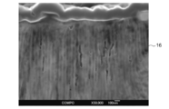
- FIG. 2 is a view showing a photograph of a cross section of the heat dissipation substrate taken with a scanning electron microscope.
- FIG. 3 is a view showing a photograph in which the area A in FIG. 2 is enlarged.
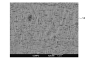
- FIG. 4 is a view showing a photograph in which the area B in FIG. 2 is enlarged.
- Radiating substrate 10 includes an aluminum layer 12, a random porous layer 14 formed on the aluminum layer 12, a vertical porous layer 16 formed on the random porous layer 14.
- the random porous layer 14 is a layer in which a large number of capsule-like elongated cavities are formed in a random direction. Specifically, in a random porous layer 14, an elongated cavity, an elongated cavity along the vertical direction with respect to the major axis direction of random porous layer 14 surface, the major axis direction of random porous layer 14 are elongated cavities along a direction inclined by a few degrees from a direction perpendicular to the surface. Most of the elongated cavities are cavities along a direction perpendicular to the surface of the random porous layer 14.
- the random porous layer 14 has a thickness of about 30 to 50 ⁇ m (41 ⁇ m in FIG. 2), the diameter of the elongated cavity is 0.01 to 0.1 ⁇ m, and the length of the cavity is that of the random porous layer 14. It is shorter than the thickness and is 0.01 to 3.0 ⁇ m.
- the elongated cavities in the random porous layer 14 include not only a linear capsule shape but also a non-linear (for example, a meandering shape) capsule shape.
- the vertical porous layer 16 has a thickness of about 1 to 3 ⁇ m (2 ⁇ m in FIG. 2), is elongated from the surface of the heat dissipation substrate 10 to the inside, and reaches the surface on the side far from the surface of the heat dissipation substrate 10. This is a layer in which a large number of substantially cylindrical micropores are not formed. The diameter of the micropore is 0.01 to 0.1 ⁇ m. In the vertical porous layer 16, the depth direction of the micropores is along a direction perpendicular to the surface of the vertical porous layer 16.
- Random porous layer 14 as described above, not only the cavity along the vertical direction to its surface, whereas the direction of the cavity of the inclined from the vertical direction angles are mixed, vertical
- the micropores in the porous layer 16 are different in that they are only micropores along a direction perpendicular to the surface of the vertical porous layer 16. Since the random porous layer 14 includes cavities with different angles, the dielectric breakdown voltage is higher than that of the vertical porous layer 16.
- Random porous layer 14 and a vertical porous layer 16 of the radiating board 10 can be formed by a liquid during plasma processing as described below.
- FIG. 5 is a diagram schematically illustrating a processing apparatus that performs plasma processing in liquid.
- the processing device 18 includes a container 20, a bubble generating device 22, a processing liquid circulation pipe 24, a circulator 26, a heat exchanger 28, an air pipe 30, and a power source 32.
- the container 20 contains a neutral or alkaline processing liquid.
- the bubble generating device 22 is provided at the bottom of the container 20, and the processing liquid circulation pipe 24 and the air pipe 30 are connected thereto.
- the bubble generating device 22 generates bubbles with the air supplied from the air pipe 30.
- Both ends of the processing liquid circulation pipe 24 are connected to the top and bottom of the container 20, and the processing liquid can be sent from the top of the container 20 to the bottom by the action of the circulator 26. Thereby, the processing liquid in the container 20 is circulated.
- the heat exchanger 28 cools the temperature of the processing liquid using external cooling water.
- the component 34 (Al substrate) to be subjected to the plasma treatment in liquid is connected to the positive electrode of the power supply 32 and functions as an anode.
- the negative electrode of the power source 32 is connected to a cathode 36 that is immersed in the processing liquid in the container 20. In this state, when an alternating current is applied between the component 34 and the cathode 36, plasma discharge (micro arc) is generated in the processing liquid.
- the above-described heat dissipation substrate 10 can be obtained by appropriately adjusting the AC waveform, processing time, type of processing solution, concentration, and the like.
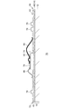
- FIG. 6 is a schematic diagram showing a method for a dielectric strength test of the heat dissipation board of the present embodiment.
- the heat dissipation substrate 10 shown in FIG. 6 has a thickness of about 1 mm.
- a random porous layer 14 and a vertical porous layer 16 are laminated on both sides of the aluminum layer 12. Then, an AC voltage is applied between the aluminum layer 12 and the surface of one vertical porous layer 16.
- dielectric breakdown did not occur in the heat dissipation substrate 10 even at an applied voltage of 3.0 kV.
- the heat dissipation substrate 10 has a dielectric breakdown voltage performance (about 1.0 kV) of an Al substrate on which an aluminum oxide film (hereinafter referred to as “aluminum oxide film”) formed by a conventional anodic oxidation method is formed. Compared with high withstand voltage performance.
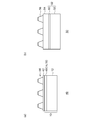
- FIG. 7A is a schematic cross-sectional view of an element mounting substrate according to the first embodiment
- FIG. 7B is a schematic cross-sectional view of an element mounting substrate according to a comparative example.
- the element mounting substrate 40 includes a heat dissipation substrate 10, an insulating resin layer 42 stacked on the heat dissipation substrate 10, and a wiring layer 44 stacked on the insulating resin layer 42.
- the heat dissipation substrate 10 includes an aluminum layer 12 and a plasma treatment film 46 including at least the random porous layer 14.
- the random porous layer 14 is provided so as to face the insulating resin layer 42.
- a copper (Cu) wiring is used for example, a power module that generates a relatively large amount of heat is mounted on the wiring layer 44.
- the element mounting substrate 40 can improve the heat dissipation performance by the heat dissipation substrate 10. Further, in order to improve withstand voltage performance of the radiating board 10 by the action of a random porous layer 14, it is possible to satisfy the dielectric strength performance required as the device mounting board 40 even if the thickness of the insulating resin layer 42 . Moreover, since the insulating resin layer 42 becomes thin, the heat dissipation performance is further improved.
- the heat dissipation substrate 10 may further include a vertical porous layer 16 that is formed closer to the insulating resin layer 42 than the random porous layer 14.
- Vertical porous layer 16 which is formed a cylindrical micropores from the surface toward the interior, for example, adhesive component of the insulating resin layer 42 by entering the micropores, the heat dissipation substrate 10 and the insulating resin layer Adhesion with 42 is improved.
- the device mounting board 50 according to the comparative example the insulating resin layer 54 is laminated on the heat dissipating substrate 52 is laminated on the insulating resin layer 54 A wiring layer 56.
- the heat dissipation substrate 52 has an aluminum layer 58 and an aluminum oxide film 60.
- Aluminum oxide film 60 because it does not have sufficient dielectric strength performance, to satisfy a predetermined withstand voltage performance required between the wiring layer 56 and the aluminum layer 58, increasing the thickness of the insulating resin layer 54 There is a need.
- the element mounting substrate 50 according to the comparative example has lower heat dissipation performance than the element mounting substrate 40 according to the present embodiment.
- FIG. 8 is a schematic cross-sectional view of a semiconductor module according to the second embodiment.
- the semiconductor module 70 includes a heat dissipation substrate 10, an insulating resin layer 42, a wiring layer 72 on which the power module is mounted, a heat spreader 74, a chip component 76, an IGBT (Insulated Gate Bipolar Transistor) 78, and an FWD (Free). Wheeling Diode) 80.
- IGBT Insulated Gate Bipolar Transistor
- FWD Free). Wheeling Diode
- the heat dissipation substrate 10 includes an aluminum layer 12 having a thickness of 1.5 mm and a plasma treatment film 46 having a thickness of 40 ⁇ m.
- the plasma processing film 46 includes at least the random porous layer 14.
- the insulating resin layer 42 laminated on the heat dissipation substrate 10 has a thickness of about 30 ⁇ m.
- the wiring layer 72 includes a copper wiring 82 having a thickness of 70 ⁇ m and a solder resist 84 having a thickness of 100 ⁇ m.
- the chip component 76 is a passive element such as a capacitor or a resistor, for example, and is mounted on the copper wiring 82 exposed from the opening of the solder resist 84.
- the IGBT 78 and the FWD 80 to which a high voltage is applied and which generate a large amount of heat are mounted on the wiring layer 72 via the heat spreader 74.
- the IGBT 78 and the FWD 80 are connected to the copper wiring 82 via Al wires 86 and 88 having a diameter of about 200 to 500 ⁇ m.
- the semiconductor module 70 can improve the heat dissipation performance by the heat dissipation substrate 10. Moreover, since the dielectric breakdown voltage performance of the heat dissipation substrate 10 is improved by the action of the random porous layer 14, the dielectric breakdown voltage performance required for the semiconductor module 70 can be satisfied even if the thickness of the insulating resin layer 42 is reduced. Since the insulating resin layer 42 is thinned, the heat dissipation performance is further improved. Thus, the heat dissipation substrate 10 is suitable for a power module substrate that is applied with a high voltage and generates a large amount of heat, such as the IGBT 78 and the FWD 80.
- FIG. 9 is a schematic diagram showing a schematic configuration of the battery module according to the third embodiment.
- the battery module 110 includes a plurality of batteries (single cells) 130 that are arranged apart from each other, and a circuit board 112 that electrically connects external terminals of the plurality of batteries (the positive electrode terminal 150 and the negative electrode terminal 160), The heat dissipating fins 114 that support the bottom (lower) regions of the plurality of batteries 130 opposite to the external terminals, and the control ICs 116 mounted on the circuit board 112 are provided.
- the circuit board 112 includes a heat dissipation board 118, an insulating resin layer 120, and a wiring layer 122.
- the heat dissipation substrate 118 is disposed on one main surface of the insulating resin layer 120.
- the heat dissipation board 118 is a member in which a metal such as Al or Mg having excellent thermal conductivity is formed into a flat plate shape, and improves the heat dissipation performance of the circuit board 112.
- the insulating resin layer 120 examples include melamine derivatives such as BT resin, thermosetting resins such as liquid crystal polymer, epoxy resin, PPE resin, polyimide resin, fluororesin, phenol resin, and polyamide bismaleimide. From the viewpoint of improving the heat dissipation of the circuit board 112, it is desirable that the insulating resin layer 120 has high thermal conductivity. For this reason, it is preferable that the insulating resin layer 120 contains silver, bismuth, copper, aluminum, magnesium, tin, zinc, an alloy thereof, and the like as a highly thermally conductive filler.
- the wiring layer 122 is formed in a predetermined pattern on the other main surface of the insulating resin layer 120.
- the wiring layer 122 of the present embodiment is made of copper.
- a control IC 116 that is an electronic component is mounted on the wiring layer 122.
- the electronic component may be a passive element such as a resistor or a capacitor.
- the control IC 116 constitutes a circuit unit that monitors the voltage and temperature of the battery 130 and controls the connection state of the battery 130. More specifically, the circuit unit monitors the voltage and temperature of each battery 130, and when the voltage or temperature indicates abnormality, disconnects only the battery 130 or a plurality of batteries including the battery 130. It has a function to do.
- a battery 130 is connected to one main surface of the circuit board 112. Specifically, external terminals (positive terminal 150 and negative terminal 160) of battery 130 and wiring layer 122 of circuit board 112 are connected.
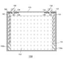
- FIG. 10 is a cross-sectional view showing a schematic configuration of the battery 130.
- the battery 130 includes an outer can (housing) 131 in which an electrode body 132 in which positive and negative electrodes are wound in a spiral shape is stored laterally with respect to the can axis direction of the outer can 131.
- the opening of the outer can 131 is sealed by the sealing plate 133.
- the positive terminal 150 and negative terminal 160 projecting outward of the battery 130 is provided on the sealing plate 133.
- the sealing plate 133 is formed with a gas discharge valve (not shown).
- the positive electrode terminal 150 is fitted into the positive electrode opening of the sealing plate 133 while being in contact with the gasket 134.
- the positive electrode terminal 150 is connected to the positive electrode tab member 153 on the battery inner side of the sealing plate 133.
- the end of the positive electrode terminal 150 fitted into the positive electrode opening of the sealing plate 133 is provided with a recess 151 in which a side wall is formed along the positive electrode opening of the sealing plate 133.
- the positive terminal 150 is fixed by caulking so that the edge portion of the recess 151 is widened.
- the core part (not shown) of the positive electrode terminal 150 is made of aluminum, and a copper plating layer (not shown) covers the periphery of the core part.
- An insulating plate 135 is provided between the positive electrode tab member 153 and the battery inner surface of the sealing plate 133.
- the insulating plate 135 and the gasket 134 are in contact with each other at the positive electrode opening of the sealing plate 133. Thereby, the positive electrode tab member 153 and the positive electrode terminal 150 are insulated from the sealing plate 133.
- the positive electrode tab member 153 is connected to the positive electrode current collector plate group 132 a protruding from one end face of the electrode body 132.
- the positive current collector plate group 132 a is a bundle of a plurality of positive current collector plates protruding from one end face of the electrode body 132.
- the negative electrode terminal 160 is fitted into the negative electrode opening of the sealing plate 133 while being in contact with the gasket 134. Further, the negative electrode terminal 160 is connected to the negative electrode tab member 162 inside the battery of the sealing plate 133. Note that a recess 161 is formed at the end of the negative electrode terminal 160 fitted into the negative electrode opening of the sealing plate 133 so that a side wall is formed along the negative electrode opening of the sealing plate 133. The negative terminal 160 is fixed by caulking so that the edge portion of the recess 161 is widened. The whole negative electrode terminal 160 is made of copper. An insulating plate 135 is provided between the negative electrode tab member 162 and the battery inner surface of the sealing plate 133. In the negative electrode opening of the sealing plate 133, the insulating plate 135 and the gasket 134 are in contact with each other. Thereby, the negative electrode tab member 162 and the negative electrode terminal 160 are insulated from the sealing plate 133.
- the negative electrode tab member 162 is connected to the negative electrode current collector plate group 132 b protruding from the other end surface of the electrode body 132.
- the negative electrode current collector plate group 132 b is a bundle of a plurality of negative electrode current collector plates protruding from the other end face of the electrode body 132.
- the battery 130 has the positive electrode terminal 150 and the negative electrode terminal 160 as the external terminals electrically connected to the electrode body 132.
- the battery 130 is disposed between the heat dissipation substrate 118 and the heat dissipation fins 114.
- the heat dissipating substrate 118 has substantially the same structure as the heat dissipating substrate 10 described above, except that the plasma treatment film 46 is provided on both surfaces of the aluminum layer 12 instead of one surface.
- the heat of the battery 130 is radiated through the heat radiating substrate 118 and the heat radiating fins 114.
- the battery module 110 includes an electrode body 132, an outer can 131 in which the electrode body is housed, provided outside the outer can 131 is electrically connected to the electrode body 132 have been and external terminal (positive terminal 150 and negative terminal 160) and, respectively, the circuit board 112 with a plurality of batteries 130 that are arranged to each other, as a connection member for electrically connecting the external terminals of the plurality of batteries 130 And comprising.
- the heat dissipation substrate 118 is provided so as to face the insulating resin layer 120, and has the random porous layer 14 in which elongated cavities are formed in random directions.
- the heat dissipation performance of the battery module 110 is improved by the heat dissipation board 118 for the same reason as described in the above embodiment.
- the withstand voltage performance of the heat dissipation substrate 118 is improved by the action of the random porous layer 14, the thickness of the insulating resin layer 120 can be reduced. As a result, the heat dissipation performance can be further improved.
- the plasma processing film 46 is also formed on the side opposite to the insulating resin layer 120 side. As described above, the plasma-treated film 46 has high withstand voltage performance due to the function of the included random porous layer 14. Therefore, it is not necessary to cover the outer surface of the heat dissipation substrate 118 with an insulating film or the like, and the heat dissipation performance is further improved.
- the heat dissipation substrate 118 may further include the vertical porous layer 16 formed in the insulating resin layer 120 rather than the random porous layer 14. Thereby, the adhesiveness between the heat dissipation substrate 118 and the insulating resin layer 120 is improved via the vertical porous layer 16.
- the withstand voltage performance improves by forming the above-mentioned random porous layer 14 on the inner surface side of the outer can 131. Therefore, the thickness of the insulating resin layer covering the inner surface of the outer can 131 can be reduced, or the insulating resin layer can be omitted. As a result, the heat dissipation performance can be further improved.
- the present invention has been described with reference to the above-described embodiments.
- the present invention is not limited to the above-described embodiments, and the configurations of the embodiments are appropriately combined or replaced. Those are also included in the present invention. Further, it is possible to appropriately change the combination and processing order in each embodiment based on the knowledge of those skilled in the art and to add various modifications such as various design changes to each embodiment. Embodiments to which is added can also be included in the scope of the present invention.
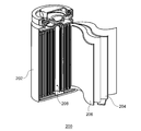
- FIG. 11 is a cross-sectional view according to a modification of the battery.
- an electrode body 208 in which a positive electrode plate 204 and a negative electrode plate 206 are wound in a spiral shape is accommodated in a cylindrical outer can 202 in parallel with the can axis direction of the outer can 202.
- Such an outer can 202 may be made of a material containing at least one metal selected from the group consisting of Al, Mg, and Ti.
- the random porous layer 14 on the inner surface side of the outer can 202, the withstand voltage performance of the battery 200 is improved. Therefore, the thickness of the insulating resin layer covering the outer surface of the outer can 202 can be reduced, or the insulating resin layer can be omitted. As a result, the heat dissipation performance of the battery 200 can be further improved.
- the element mounting substrate for the power module, the battery module, the battery, and the like have been described as examples of the components that generate heat due to the current that flows during use.
- the components are not limited to these, and the present invention can be applied to all electrical devices and electronic components that are required to have dielectric strength performance.
- the present invention can be used for an element mounting substrate.
Landscapes
- Engineering & Computer Science (AREA)
- Chemical & Material Sciences (AREA)
- Chemical Kinetics & Catalysis (AREA)
- Electrochemistry (AREA)
- General Chemical & Material Sciences (AREA)
- Microelectronics & Electronic Packaging (AREA)
- Manufacturing & Machinery (AREA)
- Inorganic Chemistry (AREA)
- Cooling Or The Like Of Semiconductors Or Solid State Devices (AREA)
- Sealing Battery Cases Or Jackets (AREA)
- Secondary Cells (AREA)
- Battery Mounting, Suspending (AREA)
- Connection Of Batteries Or Terminals (AREA)
- Insulated Metal Substrates For Printed Circuits (AREA)
Abstract
素子搭載用基板40は、Al、MgおよびTiからなる群より選択される少なくとも一つの金属を含む材料で構成されている放熱基板10と、放熱基板の上に積層されている絶縁樹脂層42と、絶縁樹脂層の上に積層されている、パワーモジュールが搭載される配線層44と、を備える。放熱基板10は、絶縁樹脂層42と対向するように設けられ、細長形状の空洞がランダムな方向に形成されているランダム多孔質層14を有する。
Description
本発明は、部品の放熱基板の技術に関する。
従来、IGBT(Insulated Gate Bipolar Transistor)等に代表されるパワーモジュールの開発が進められている。そのパワーモジュールは高電圧が印加されることから発熱量もかなり大きくなる。そのため、放熱性向上のために、パワーモジュールを金属基板上に搭載する構造が採用されている。その金属基板としては、軽量かつ熱伝導性に優れたアルミニウム合金の採用が進んでいる。
このような場合、アルミニウム基板に樹脂基板を高強度で接着させることが求められる。そこで、良好な酸化皮膜を高精度に形成することで、樹脂製絶縁材との接着性を向上させることができる、とされているプリント回路用アルミニウム基板が考案されている(特許文献1参照)
しかしながら、前述のアルミニウム基板に形成されている酸化皮膜は、十分な絶縁耐圧性能がないため、アルミニウム基板と密着する樹脂製絶縁材の厚みを厚くする必要がある。そのため、プリント基板の放熱性の観点では更に改善の余地がある。
本発明はこうした状況に鑑みてなされたものであり、その目的とするところは、使用時に流れる電流によって発熱する部品の絶縁耐圧性能と放熱性能とを両立できる技術を提供することにある。
上記課題を解決するために、本発明のある態様の素子搭載用基板は、Al、MgおよびTiからなる群より選択される少なくとも一つの金属を含む材料で構成されている放熱基板と、放熱基板の上に積層されている絶縁樹脂層と、絶縁樹脂層の上に積層されている、パワーモジュールが搭載される配線層と、を備える。放熱基板は、絶縁樹脂層と対向するように設けられ、細長形状の空洞がランダムな方向に形成されているランダム多孔質層を有する。
この態様によると、放熱基板により放熱性能を向上することができる。また、ランダム多孔質層の働きにより放熱基板の絶縁耐圧性能が向上するため、絶縁樹脂層の厚みを薄くすることができる。その結果、放熱性能を更に向上することができる。
放熱基板は、ランダム多孔質層よりも絶縁樹脂層側に形成されている縦型多孔質層を更に有してもよい。縦型多孔質層は、放熱基板の表面から内部に向かって円筒状の微小孔が形成されていてもよい。これにより、縦型多孔質層を介して放熱基板と絶縁樹脂層との密着性が向上する。
本発明の別の態様は、電池である。この電池は、電極体と、電極体が収容され、Al、MgおよびTiからなる群より選択される少なくとも一つの金属を含む材料で構成されている筐体と、筐体の外部に設けられ、電極体に電気的に接続されている外部端子とを備える。筐体は、細長形状の空洞がランダムな方向に形成されているランダム多孔質層が筐体の内面側に形成されている。
この態様によると、筐体により放熱性能を向上することができる。また、ランダム多孔質層の働きにより筐体の絶縁耐圧性能が向上するため、筐体の内面に形成する絶縁樹脂層の厚みを薄くする、または、絶縁樹脂層をなくすことができる。その結果、放熱性能を更に向上することができる。
本発明の更に別の態様は、電池モジュールである。この電池モジュールは、電極体と、電極体が収容された筐体と、筐体の外部に設けられ、電極体に電気的に接続されている外部端子とをそれぞれ有し、互いに配列された複数の電池と、複数の電池の外部端子同士を電気的に接続する接続部材と、を備える。接続部材は、Al、MgおよびTiからなる群より選択される少なくとも一つの金属を含む材料で構成されている放熱基板と、放熱基板の上に積層されている絶縁樹脂層と、絶縁樹脂層の上に積層され、外部端子同士を導通する配線層と、を有する。放熱基板は、絶縁樹脂層と対向するように設けられ、細長形状の空洞がランダムな方向に形成されているランダム多孔質層を有する。
この態様によると、放熱基板により放熱性能を向上することができる。また、ランダム多孔質層の働きにより放熱基板の絶縁耐圧性能が向上するため、絶縁樹脂層の厚みを薄くすることができる。その結果、放熱性能を更に向上することができる。
放熱基板は、ランダム多孔質層よりも絶縁樹脂層側に形成されている縦型多孔質層を更に有してもよい。縦型多孔質層は、放熱基板の表面から内部に向かって円筒状の微小孔が形成されていてもよい。これにより、縦型多孔質層を介して放熱基板と絶縁樹脂層との密着性が向上する。
本発明によれば、使用時に流れる電流によって発熱する部品の絶縁耐圧性能と放熱性能とを両立できる。
以下、図面を参照しながら、本発明を実施するための形態について詳細に説明する。なお、図面の説明において同一の要素には同一の符号を付し、重複する説明を適宜省略する。なお、以下の各図に示す各層、各部の縮尺や形状は、説明を容易にするために便宜的に設定されており、特に言及がない限り限定的に解釈されるものではない。
(第1の実施の形態)
[放熱基板]
放熱基板は、Al、MgおよびTiからなる群より選択される少なくとも一つの金属を含む材料で構成されている。なお、放熱性能や軽量化、コストの観点から、アルミニウムがより好適である。以下では、アルミニウムを用いた放熱基板を例に説明する。
[放熱基板]
放熱基板は、Al、MgおよびTiからなる群より選択される少なくとも一つの金属を含む材料で構成されている。なお、放熱性能や軽量化、コストの観点から、アルミニウムがより好適である。以下では、アルミニウムを用いた放熱基板を例に説明する。
図1は、第1の実施の形態に係る放熱基板を模式的に示した図である。図2は、放熱基板の断面を走査型電子顕微鏡で撮影した写真を示す図である。図3は、図2のA領域を拡大した写真を示す図である。図4は、図2のB領域を拡大した写真を示す図である。
放熱基板10は、アルミニウム層12と、アルミニウム層12の上に形成されているランダム多孔質層14と、ランダム多孔質層14の上に形成されている縦型多孔質層16と、を有する。ランダム多孔質層14は、その層内に多数のカプセル状の細長い空洞がランダムな方向に形成されている層である。具体的には、ランダム多孔質層14内において、細長い空洞は、その長軸方向がランダム多孔質層14表面に対して鉛直な方向に沿った細長い空洞と、その長軸方向がランダム多孔質層14表面に対して鉛直な方向から数度の角度だけ傾いた方向に沿った細長い空洞とが混在している。細長い空洞のうちほとんどが、ランダム多孔質層14表面に対して鉛直な方向に沿った空洞である。
なお、ランダム多孔質層14は、厚みが30~50μm程度(図2では41μm)であり、細長い空洞の直径は、0.01~0.1μm、空洞の長さは、ランダム多孔質層14の厚みよりも短く、0.01~3.0μmである。また、ランダム多孔質層14内の細長い空洞は、直線状のカプセル形状のものだけでなく、非直線状(例えば、蛇行した形状)のカプセル形状のものも含まれている。
縦型多孔質層16は、厚みが1~3μm程度(図2では2μm)であり、放熱基板10の表面から内部に向かって、細長くかつ放熱基板10の表面から遠い側の面には達していない概ね円筒形状の微小孔が多数形成されている層である。微小孔の直径は、0.01~0.1μmである。縦型多孔質層16においては、微小孔の深さ方向は縦型多孔質層16の表面に対して鉛直な方向に沿っている。
ランダム多孔質層14は、上述のとおり、その表面に対して鉛直な方向に沿った空洞だけでなく、鉛直な方向から傾いた角度の方向の空洞が混在しているのに対して、縦型多孔質層16内の微小孔は、縦型多孔質層16の表面に対して鉛直な方向に沿った微小孔だけである点で異なる。ランダム多孔質層14は角度の異なる空洞が混在していることから、縦型多孔質層16よりも絶縁耐圧が高い。
[液中プラズマ処理]
放熱基板10のランダム多孔質層14や縦型多孔質層16は、以下に述べる液中プラズマ処理により形成することができる。図5は、液中プラズマ処理を行う処理装置の概略を示す図である。
放熱基板10のランダム多孔質層14や縦型多孔質層16は、以下に述べる液中プラズマ処理により形成することができる。図5は、液中プラズマ処理を行う処理装置の概略を示す図である。
処理装置18は、容器20、気泡発生装置22、処理液循環配管24、循環器26、熱交換器28、空気配管30および電源32を備える。容器20は、中性またはアルカリ性の処理液を収容する。気泡発生装置22は、容器20の底部に設けられており、処理液循環配管24および空気配管30が接続されている。そして、気泡発生装置22は、空気配管30から供給される空気により気泡を発生させる。
処理液循環配管24は、その両端が容器20の上部と底部に接続されており、循環器26の働きによって処理液を容器20の上部から底部へ送ることができる。それによって、容器20内の処理液が循環される。熱交換器28は、外部の冷却水を用いて処理液の温度を冷却する。
液中プラズマ処理の対象となる部品34(Al基板)は、電源32の正極と接続され、陽極として機能する。また、電源32の負極は、容器20内の処理液に浸漬している陰極36と接続されている。この状態で、部品34と陰極36との間に交流が印加されると、処理液中でプラズマ放電(マイクロアーク)が生じる。交流の波形、処理時間、処理液の種類、濃度などを適宜調整することで、前述の放熱基板10が得られる。
図6は、本実施の形態の放熱基板の絶縁耐圧試験の方法を示す模式図である。図6に示す放熱基板10は、厚みが約1mmである。放熱基板10は、アルミニウム層12の両側にそれぞれランダム多孔質層14および縦型多孔質層16が積層されている。そして、アルミニウム層12と一方の縦型多孔質層16の表面との間に交流電圧を印加する。その結果、本実施の形態に係る放熱基板10では、3.0kVの印加電圧でも放熱基板10において絶縁破壊は生じなかった。つまり、本実施の形態に係る放熱基板10は、従来の陽極酸化法で形成したアルミ酸化皮膜(以下、「アルミ酸化皮膜」という)を形成したAl基板の絶縁耐圧性能(約1.0kV)と比較して、高い絶縁耐圧性能を有する。
図7(a)は、第1の実施の形態に係る素子搭載用基板の概略断面図、図7(b)は、比較例に係る素子搭載用基板の概略断面図である。
素子搭載用基板40は、放熱基板10と、放熱基板10の上に積層されている絶縁樹脂層42と、絶縁樹脂層42の上に積層されている配線層44と、を備える。放熱基板10は、アルミニウム層12と、少なくともランダム多孔質層14を含むプラズマ処理膜46とを有する。ランダム多孔質層14は、絶縁樹脂層42と対向するように設けられている。配線層44は、例えば、銅(Cu)配線が用いられる。配線層44には、例えば、発熱量が比較的多いパワーモジュールが搭載される。
上述のように、本実施の形態に係る素子搭載用基板40は、放熱基板10により放熱性能を向上することができる。また、ランダム多孔質層14の働きにより放熱基板10の絶縁耐圧性能が向上するため、絶縁樹脂層42の厚みを薄くしても素子搭載用基板40として要求される絶縁耐圧性能を満たすことができる。また、絶縁樹脂層42が薄くなることで、放熱性能が更に向上する。
なお、放熱基板10は、ランダム多孔質層14よりも絶縁樹脂層42側に形成されている縦型多孔質層16を更に有してもよい。縦型多孔質層16は、表面から内部に向かって円筒状の微小孔が形成されているため、例えば、絶縁樹脂層42の接着成分が微小孔に入り込むことで、放熱基板10と絶縁樹脂層42との密着性が向上する。
一方、図7(b)に示すように、比較例に係る素子搭載用基板50は、放熱基板52の上に積層されている絶縁樹脂層54と、絶縁樹脂層54の上に積層されている配線層56と、を備える。放熱基板52は、アルミニウム層58と、アルミ酸化皮膜60とを有する。アルミ酸化皮膜60は、十分な絶縁耐圧性能を有していないため、配線層56とアルミニウム層58との間で必要な所定の絶縁耐圧性能を満たすには、絶縁樹脂層54の厚みを厚くする必要がある。その結果、比較例に係る素子搭載用基板50は、本実施の形態に係る素子搭載用基板40と比較して放熱性能が低下してしまう。
(第2の実施の形態)
図8は、第2の実施の形態に係る半導体モジュールの概略断面図である。図8に示すように、半導体モジュール70は、放熱基板10、絶縁樹脂層42、パワーモジュールが搭載される配線層72、ヒートスプレッダ74、チップ部品76、IGBT(Insulated Gate Bipolar Transistor)78およびFWD(Free Wheeling Diode)80を備える。
図8は、第2の実施の形態に係る半導体モジュールの概略断面図である。図8に示すように、半導体モジュール70は、放熱基板10、絶縁樹脂層42、パワーモジュールが搭載される配線層72、ヒートスプレッダ74、チップ部品76、IGBT(Insulated Gate Bipolar Transistor)78およびFWD(Free Wheeling Diode)80を備える。
放熱基板10は、厚さ1.5mmのアルミニウム層12と、厚さ40μmのプラズマ処理膜46とからなる。プラズマ処理膜46は、少なくともランダム多孔質層14を含んでいる。放熱基板10の上に積層されている絶縁樹脂層42は、厚さが約30μmである。配線層72は、厚さ70μmの銅配線82と、厚さ100μmのソルダーレジスト84とからなる。チップ部品76は、例えば、コンデンサや抵抗などの受動素子であり、ソルダーレジスト84の開口部から露出している銅配線82に搭載されている。
高電圧が印加され発熱量も多いIGBT78およびFWD80は、ヒートスプレッダ74を介して配線層72に搭載されている。IGBT78およびFWD80は、直径が200~500μm程度のAlワイヤ86,88を介して、銅配線82と接続されている。
上述のように、本実施の形態に係る半導体モジュール70は、放熱基板10により放熱性能を向上することができる。また、ランダム多孔質層14の働きにより放熱基板10の絶縁耐圧性能が向上するため、絶縁樹脂層42の厚みを薄くしても半導体モジュール70として要求される絶縁耐圧性能を満たすことができる。絶縁樹脂層42が薄くなることで、放熱性能が更に向上する。このように、放熱基板10は、IGBT78およびFWD80のように高電圧が印加され発熱量も多いパワーモジュール用基板に好適である。
(第3の実施の形態)
[電池モジュール]
図9は、第3の実施の形態に係る電池モジュールの概略構成を示す模式図である。電池モジュール110は、互いに離間して配列されている複数の電池(単セル)130と、複数の電池の外部端子同士(正極端子150および負極端子160)を電気的に接続する回路基板112と、複数の電池130の、外部端子と反対側の底部(下部)領域を支持する放熱フィン114と、回路基板112に搭載されている制御IC116と、を備える。
[電池モジュール]
図9は、第3の実施の形態に係る電池モジュールの概略構成を示す模式図である。電池モジュール110は、互いに離間して配列されている複数の電池(単セル)130と、複数の電池の外部端子同士(正極端子150および負極端子160)を電気的に接続する回路基板112と、複数の電池130の、外部端子と反対側の底部(下部)領域を支持する放熱フィン114と、回路基板112に搭載されている制御IC116と、を備える。
[回路基板]
回路基板112は、放熱基板118、絶縁樹脂層120および配線層122を有する。放熱基板118は、絶縁樹脂層120の一方の主表面に配置されている。放熱基板118は、熱伝導性に優れたAl、Mgなどの金属を平板状にした部材であり、回路基板112の放熱性を高める。
回路基板112は、放熱基板118、絶縁樹脂層120および配線層122を有する。放熱基板118は、絶縁樹脂層120の一方の主表面に配置されている。放熱基板118は、熱伝導性に優れたAl、Mgなどの金属を平板状にした部材であり、回路基板112の放熱性を高める。
絶縁樹脂層120は、例えば、BTレジン等のメラミン誘導体、液晶ポリマー、エポキシ樹脂、PPE樹脂、ポリイミド樹脂、フッ素樹脂、フェノール樹脂、ポリアミドビスマレイミド等の熱硬化性樹脂が例示される。回路基板112の放熱性向上の観点から、絶縁樹脂層120は高熱伝導性を有することが望ましい。このため、絶縁樹脂層120は、銀、ビスマス、銅、アルミニウム、マグネシウム、錫、亜鉛およびこれらの合金などを高熱伝導性フィラーとして含有することが好ましい。
配線層122は、絶縁樹脂層120の他方の主表面に所定パターンをなして形成されている。本実施の形態の配線層122は銅で形成されている。
配線層122には、電子部品である制御IC116が搭載されている。電子部品としては、制御IC以外にも、抵抗、コンデンサなどの受動素子であってもよい。制御IC116は、電池130の電圧や温度を監視し、電池130の接続状態を制御する回路部を構成する。より具体的には、回路部は、各電池130の電圧や温度を監視し、電圧や温度が異常を示した場合に、当該電池130のみ、または当該電池130を含む複数の電池の接続を遮断する機能等を備えている。
また、回路基板112の一方の主表面には、電池130が接続されている。具体的には、電池130の外部端子(正極端子150および負極端子160)と回路基板112の配線層122とが接続されている。
[電池]
図10は、電池130の概略構成を示す断面図である。電池130は、図10に示すように、外装缶(筐体)131内に、正負極が渦巻状に巻回されてなる電極体132が外装缶131の缶軸方向に対し横向きに収納されており、封口板133により外装缶131の開口が封口されている。封口板133には電池130の外方に突出した正極端子150と負極端子160が設けられている。また、封口板133には、ガス排出弁(図示せず)が形成されている。
図10は、電池130の概略構成を示す断面図である。電池130は、図10に示すように、外装缶(筐体)131内に、正負極が渦巻状に巻回されてなる電極体132が外装缶131の缶軸方向に対し横向きに収納されており、封口板133により外装缶131の開口が封口されている。封口板133には電池130の外方に突出した正極端子150と負極端子160が設けられている。また、封口板133には、ガス排出弁(図示せず)が形成されている。
正極端子150は、ガスケット134に当接された状態で、封口板133の正極用開口に嵌め込まれている。また、正極端子150は、封口板133の電池内側において正極タブ部材153と接続している。なお、封口板133の正極用開口に嵌め込まれた正極端子150の端部には、封口板133の正極用開口に沿って側壁が形成されるような凹部151が設けられている。凹部151の縁部分が広がるようにかしめることで、正極端子150が固定されている。正極端子150の芯部(図示せず)はアルミニウムで形成されており、芯部の周りを銅めっき層(図示せず)が被覆している。正極タブ部材153と封口板133の電池内側面との間に絶縁板135が設けられている。封口板133の正極用開口において、絶縁板135とガスケット134とが当接している。これにより、正極タブ部材153および正極端子150が封口板133から絶縁されている。
正極タブ部材153は、電極体132の一方の端面から突出した正極集電板群132aに接続されている。なお、正極集電板群132aは、電極体132の一方の端面から突出した複数の正極集電板を束ねたものである。
負極端子160は、ガスケット134に当接された状態で、封口板133の負極用開口に嵌め込まれている。また、負極端子160は、封口板133の電池内側において負極タブ部材162と接続している。なお、封口板133の負極用開口に嵌め込まれた負極端子160の端部には、封口板133の負極用開口に沿って側壁が形成されるような凹部161が設けられている。凹部161の縁部分が広がるようにかしめることで、負極端子160が固定されている。負極端子160は全体が銅で形成されている。負極タブ部材162と封口板133の電池内側面との間に絶縁板135が設けられている。封口板133の負極用開口において、絶縁板135とガスケット134とが当接している。これにより、負極タブ部材162および負極端子160が封口板133から絶縁されている。
負極タブ部材162は、電極体132の他方の端面から突出した負極集電板群132bに接続されている。なお、負極集電板群132bは、電極体132の他方の端面から突出した複数の負極集電板を束ねたものである。
このように、本実施の形態に係る電池130は、電極体132に電気的に接続されている外部端子として、正極端子150および負極端子160を有している。
図9に示す電池モジュール110においては、電池130は放熱基板118と放熱フィン114との間に配置されている。放熱基板118は、前述の放熱基板10とほぼ同様の構成であり、プラズマ処理膜46がアルミニウム層12の片面ではなく両面に設けられている点が異なる。電池130の熱は放熱基板118や放熱フィン114を介して放熱される。
上述のように、本実施の形態に係る電池モジュール110は、電極体132と、電極体が収容された外装缶131と、外装缶131の外部に設けられ、電極体132に電気的に接続されている外部端子(正極端子150および負極端子160)とをそれぞれ有し、互いに配列された複数の電池130と、複数の電池130の外部端子同士を電気的に接続する接続部材としての回路基板112と、を備える。
回路基板112は、Al、MgおよびTiからなる群より選択される少なくとも一つの金属を含む材料で構成されている放熱基板118と、放熱基板118の上に積層されている絶縁樹脂層120と、絶縁樹脂層120の上に積層され、外部端子同士を導通する配線層122と、を有する。放熱基板118は、絶縁樹脂層120と対向するように設けられ、細長形状の空洞がランダムな方向に形成されているランダム多孔質層14を有する。
したがって、電池モジュール110は、前述の実施の形態で述べた理由と同様に、放熱基板118により放熱性能が向上する。またランダム多孔質層14の働きにより放熱基板118の絶縁耐圧性能が向上するため、絶縁樹脂層120の厚みを薄くすることができる。その結果、放熱性能を更に向上することができる。また、本実施の形態に係る放熱基板118は、絶縁樹脂層120側と反対側にもプラズマ処理膜46が形成されている。プラズマ処理膜46は、前述のように、含まれているランダム多孔質層14の働きにより絶縁耐圧性能が高い。そのため、放熱基板118の外側の面を絶縁フィルムなどで覆う必要がなくなり、放熱性能が更に向上する。
放熱基板118は、ランダム多孔質層14よりも絶縁樹脂層120に形成されている縦型多孔質層16を更に有してもよい。これにより、縦型多孔質層16を介して放熱基板118と絶縁樹脂層120との密着性が向上する。
なお、電池130の外装缶131を、Al、MgおよびTiからなる群より選択される少なくとも一つの金属を含む材料で構成してもよい。そして、外装缶131の内面側に、前述のランダム多孔質層14を形成することで、絶縁耐圧性能が向上する。そのため、外装缶131の内面を覆う絶縁樹脂層の厚みを薄くする、または、絶縁樹脂層を省略できる。その結果、放熱性能を更に向上することができる。
以上、本発明を上述の各実施の形態を参照して説明したが、本発明は上述の各実施の形態に限定されるものではなく、各実施の形態の構成を適宜組み合わせたものや置換したものについても本発明に含まれるものである。また、当業者の知識に基づいて各実施の形態における組合せや処理の順番を適宜組み替えることや各種の設計変更等の変形を各実施の形態に対して加えることも可能であり、そのような変形が加えられた実施の形態も本発明の範囲に含まれうる。
図11は、電池の変形例に係る断面図である。電池200は、円筒の外装缶202の内部に正極板204と負極板206とが渦巻状に巻回されてなる電極体208が外装缶202の缶軸方向に対して平行に収納されている。このような外装缶202を、Al、MgおよびTiからなる群より選択される少なくとも一つの金属を含む材料で構成してもよい。そして、外装缶202の内面側に、前述のランダム多孔質層14を形成することで、電池200の絶縁耐圧性能が向上する。そのため、外装缶202の外面を覆う絶縁樹脂層の厚みを薄くする、または、絶縁樹脂層を省略できる。その結果、電池200の放熱性能を更に向上することができる。
なお、上述の各実施の形態では、使用時に流れる電流によって発熱する部品として、パワーモジュール用の素子搭載用基板や電池モジュール、電池などを例に説明した。しかしながら、部品はこれらに限られるものではなく、絶縁耐圧性能が求められるあらゆる電気機器、電子部品に本願発明を適用することが可能である。
10 放熱基板、 12 アルミニウム層、 14 ランダム多孔質層、 16 縦型多孔質層、 40 素子搭載用基板、 42 絶縁樹脂層、 44 配線層、 46 プラズマ処理膜、 70 半導体モジュール、 72 配線層、 78 IGBT、 80 FWD、 82 銅配線、 110 電池モジュール、 112 回路基板、 118 放熱基板、 120 絶縁樹脂層、 122 配線層、 130 電池、 131 外装缶、 132 電極体、 150 正極端子、 160 負極端子。
本発明は、素子搭載用基板に利用できる。
Claims (5)
- Al、MgおよびTiからなる群より選択される少なくとも一つの金属を含む材料で構成されている放熱基板と、
前記放熱基板の上に積層されている絶縁樹脂層と、
前記絶縁樹脂層の上に積層されている、パワーモジュールが搭載される配線層と、を備え、
前記放熱基板は、
前記絶縁樹脂層と対向するように設けられ、細長形状の空洞がランダムな方向に形成されているランダム多孔質層を有する、
ことを特徴とする素子搭載用基板。 - 前記放熱基板は、前記ランダム多孔質層よりも絶縁樹脂層側に形成されている縦型多孔質層を更に有し、
前記縦型多孔質層は、放熱基板の表面から内部に向かって円筒状の微小孔が形成されていることを特徴とする請求項1に記載の素子搭載用基板。 - 電極体と、
前記電極体が収容され、Al、MgおよびTiからなる群より選択される少なくとも一つの金属を含む材料で構成されている筐体と、
前記筐体の外部に設けられ、前記電極体に電気的に接続されている外部端子とを備え、
前記筐体は、細長形状の空洞がランダムな方向に形成されているランダム多孔質層が筐体の内面側に形成されていることを特徴とする電池。 - 電極体と、前記電極体が収容された筐体と、前記筐体の外部に設けられ、前記電極体に電気的に接続されている外部端子とをそれぞれ有し、互いに配列された複数の電池と、
複数の前記電池の外部端子同士を電気的に接続する接続部材と、を備え、
前記接続部材は、
Al、MgおよびTiからなる群より選択される少なくとも一つの金属を含む材料で構成されている放熱基板と、
前記放熱基板の上に積層されている絶縁樹脂層と、
前記絶縁樹脂層の上に積層され、前記外部端子同士を導通する配線層と、を有し、
前記放熱基板は、
前記絶縁樹脂層と対向するように設けられ、細長形状の空洞がランダムな方向に形成されているランダム多孔質層を有する、
ことを特徴とする電池モジュール。 - 前記放熱基板は、前記ランダム多孔質層よりも絶縁樹脂層側に形成されている縦型多孔質層を更に有し、
前記縦型多孔質層は、放熱基板の表面から内部に向かって円筒状の微小孔が形成されていることを特徴とする請求項4に記載の電池モジュール。
Priority Applications (1)
| Application Number | Priority Date | Filing Date | Title |
|---|---|---|---|
| US13/768,777 US9307630B2 (en) | 2011-03-31 | 2013-02-15 | Device mounting board, cell, and battery module |
Applications Claiming Priority (2)
| Application Number | Priority Date | Filing Date | Title |
|---|---|---|---|
| JP2011-080205 | 2011-03-31 | ||
| JP2011080205A JP2014116328A (ja) | 2011-03-31 | 2011-03-31 | 素子搭載用基板、電池および電池モジュール |
Related Child Applications (1)
| Application Number | Title | Priority Date | Filing Date |
|---|---|---|---|
| US13/768,777 Continuation US9307630B2 (en) | 2011-03-31 | 2013-02-15 | Device mounting board, cell, and battery module |
Publications (1)
| Publication Number | Publication Date |
|---|---|
| WO2012132210A1 true WO2012132210A1 (ja) | 2012-10-04 |
Family
ID=46930007
Family Applications (1)
| Application Number | Title | Priority Date | Filing Date |
|---|---|---|---|
| PCT/JP2012/001184 Ceased WO2012132210A1 (ja) | 2011-03-31 | 2012-02-22 | 素子搭載用基板、電池および電池モジュール |
Country Status (3)
| Country | Link |
|---|---|
| US (1) | US9307630B2 (ja) |
| JP (1) | JP2014116328A (ja) |
| WO (1) | WO2012132210A1 (ja) |
Cited By (1)
| Publication number | Priority date | Publication date | Assignee | Title |
|---|---|---|---|---|
| JP2015011844A (ja) * | 2013-06-28 | 2015-01-19 | 三洋電機株式会社 | 車載用の電源装置及び電源装置を備える車両並びにバスバー |
Families Citing this family (12)
| Publication number | Priority date | Publication date | Assignee | Title |
|---|---|---|---|---|
| JP6528411B2 (ja) * | 2015-01-15 | 2019-06-12 | 株式会社オートネットワーク技術研究所 | バッテリー |
| US9692096B2 (en) | 2015-06-30 | 2017-06-27 | Faraday&Future Inc. | Partially-submerged battery cells for vehicle energy-storage systems |
| US9995535B2 (en) | 2015-06-30 | 2018-06-12 | Faraday&Future Inc. | Heat pipe for vehicle energy-storage systems |
| US9692095B2 (en) | 2015-06-30 | 2017-06-27 | Faraday&Future Inc. | Fully-submerged battery cells for vehicle energy-storage systems |
| US11108100B2 (en) | 2015-06-30 | 2021-08-31 | Faraday & Future Inc. | Battery module for vehicle energy-storage systems |
| US10505163B2 (en) | 2015-06-30 | 2019-12-10 | Faraday & Future Inc. | Heat exchanger for vehicle energy-storage systems |
| US20170005303A1 (en) | 2015-06-30 | 2017-01-05 | Faraday&Future Inc. | Vehicle Energy-Storage System |
| US11258104B2 (en) | 2015-06-30 | 2022-02-22 | Faraday & Future Inc. | Vehicle energy-storage systems |
| US10826042B2 (en) | 2015-06-30 | 2020-11-03 | Faraday & Future Inc. | Current carrier for vehicle energy-storage systems |
| FR3060876A1 (fr) | 2016-12-15 | 2018-06-22 | Zodiac Aero Electric | Dispositif de connexion thermique et electrique pour equipements de distribution electrique et batteries d'un aeronef |
| US11527792B2 (en) | 2019-03-14 | 2022-12-13 | Generac Power Systems, Inc. | Battery module thermal management |
| US12374734B2 (en) * | 2019-12-16 | 2025-07-29 | Dyson Technology Limited | Battery cell with internal swelling relief and external cooling features |
Citations (7)
| Publication number | Priority date | Publication date | Assignee | Title |
|---|---|---|---|---|
| JPH02185993A (ja) * | 1988-10-14 | 1990-07-20 | Alcan Internatl Ltd | 陽極処理性金属基体表面への仕上げ金属層の被着方法 |
| JPH06334287A (ja) * | 1993-05-19 | 1994-12-02 | Furukawa Electric Co Ltd:The | アルミベースプリント配線板およびその製造方法 |
| JP2000106215A (ja) * | 1998-09-30 | 2000-04-11 | Japan Storage Battery Co Ltd | 非水電解質電池 |
| JP2004179224A (ja) * | 2002-11-25 | 2004-06-24 | Matsushita Electric Works Ltd | 金属コア基板及び金属コア配線板 |
| JP2006024906A (ja) * | 2004-06-10 | 2006-01-26 | Showa Denko Kk | プリント回路用アルミニウム基板及びその製造方法、並びにプリント基板及びその製造方法 |
| JP2008226744A (ja) * | 2007-03-15 | 2008-09-25 | Gs Yuasa Corporation:Kk | 組電池 |
| JP2010518258A (ja) * | 2007-02-16 | 2010-05-27 | エコール ポリテクニック フェデラル デ ローザンヌ | 多孔質金属品および多孔質金属品の製造方法 |
-
2011
- 2011-03-31 JP JP2011080205A patent/JP2014116328A/ja not_active Withdrawn
-
2012
- 2012-02-22 WO PCT/JP2012/001184 patent/WO2012132210A1/ja not_active Ceased
-
2013
- 2013-02-15 US US13/768,777 patent/US9307630B2/en not_active Expired - Fee Related
Patent Citations (7)
| Publication number | Priority date | Publication date | Assignee | Title |
|---|---|---|---|---|
| JPH02185993A (ja) * | 1988-10-14 | 1990-07-20 | Alcan Internatl Ltd | 陽極処理性金属基体表面への仕上げ金属層の被着方法 |
| JPH06334287A (ja) * | 1993-05-19 | 1994-12-02 | Furukawa Electric Co Ltd:The | アルミベースプリント配線板およびその製造方法 |
| JP2000106215A (ja) * | 1998-09-30 | 2000-04-11 | Japan Storage Battery Co Ltd | 非水電解質電池 |
| JP2004179224A (ja) * | 2002-11-25 | 2004-06-24 | Matsushita Electric Works Ltd | 金属コア基板及び金属コア配線板 |
| JP2006024906A (ja) * | 2004-06-10 | 2006-01-26 | Showa Denko Kk | プリント回路用アルミニウム基板及びその製造方法、並びにプリント基板及びその製造方法 |
| JP2010518258A (ja) * | 2007-02-16 | 2010-05-27 | エコール ポリテクニック フェデラル デ ローザンヌ | 多孔質金属品および多孔質金属品の製造方法 |
| JP2008226744A (ja) * | 2007-03-15 | 2008-09-25 | Gs Yuasa Corporation:Kk | 組電池 |
Cited By (1)
| Publication number | Priority date | Publication date | Assignee | Title |
|---|---|---|---|---|
| JP2015011844A (ja) * | 2013-06-28 | 2015-01-19 | 三洋電機株式会社 | 車載用の電源装置及び電源装置を備える車両並びにバスバー |
Also Published As
| Publication number | Publication date |
|---|---|
| JP2014116328A (ja) | 2014-06-26 |
| US20130157102A1 (en) | 2013-06-20 |
| US9307630B2 (en) | 2016-04-05 |
Similar Documents
| Publication | Publication Date | Title |
|---|---|---|
| JP2014116328A (ja) | 素子搭載用基板、電池および電池モジュール | |
| US10492344B2 (en) | Power module | |
| JP4027558B2 (ja) | パワーモジュール | |
| CN104303289B (zh) | 电子模块及其制造方法 | |
| US9852962B2 (en) | Waterproof electronic device and manufacturing method thereof | |
| JP5212417B2 (ja) | パワー半導体モジュール | |
| KR101321277B1 (ko) | 전력 모듈 패키지 및 그 제조방법 | |
| JP5217884B2 (ja) | 半導体装置 | |
| JP2018512742A (ja) | パワーエレクトロニクスモジュール | |
| JP2004228403A (ja) | 半導体モジュールおよびその製造方法並びにスイッチング電源装置 | |
| KR20110014867A (ko) | 전력소자 패키지 및 그 제조방법 | |
| CN101901795A (zh) | 功率半导体模块 | |
| JPWO2009069404A1 (ja) | 電池モジュール及び充電モジュール | |
| JP2020077679A (ja) | 半導体モジュールおよび車両 | |
| WO2015040902A1 (ja) | パワー半導体モジュール及びそれを用いた電力変換装置 | |
| JP2016046497A (ja) | パワー半導体装置及びパワー半導体装置の製造方法 | |
| US12062593B2 (en) | Power device assemblies and cooling devices for cooling heat-generating devices | |
| KR20180087330A (ko) | 파워 모듈의 양면 냉각을 위한 금속 슬러그 | |
| JP2019161081A (ja) | 電力変換装置及び電力変換装置の製造方法 | |
| CN113097155A (zh) | 一种芯片导热模块及其制备方法 | |
| JP2004088022A (ja) | 大電力用半導体装置 | |
| JP7286007B2 (ja) | 半導体装置、電力変換装置および半導体装置の製造方法 | |
| CN215118901U (zh) | 智能功率模块 | |
| JP5621812B2 (ja) | 半導体装置 | |
| JP2014135329A (ja) | ケース外装型コンデンサの製造方法及びケース外装型コンデンサ |
Legal Events
| Date | Code | Title | Description |
|---|---|---|---|
| 121 | Ep: the epo has been informed by wipo that ep was designated in this application |
Ref document number: 12763099 Country of ref document: EP Kind code of ref document: A1 |
|
| NENP | Non-entry into the national phase |
Ref country code: DE |
|
| 122 | Ep: pct application non-entry in european phase |
Ref document number: 12763099 Country of ref document: EP Kind code of ref document: A1 |
|
| NENP | Non-entry into the national phase |
Ref country code: JP |