WO2012132103A1 - 位相補償受信器 - Google Patents
位相補償受信器 Download PDFInfo
- Publication number
- WO2012132103A1 WO2012132103A1 PCT/JP2011/076741 JP2011076741W WO2012132103A1 WO 2012132103 A1 WO2012132103 A1 WO 2012132103A1 JP 2011076741 W JP2011076741 W JP 2011076741W WO 2012132103 A1 WO2012132103 A1 WO 2012132103A1
- Authority
- WO
- WIPO (PCT)
- Prior art keywords
- compensation
- phase
- slip
- amount
- unit
- Prior art date
Links
Images


Classifications
-
- H—ELECTRICITY
- H04—ELECTRIC COMMUNICATION TECHNIQUE
- H04L—TRANSMISSION OF DIGITAL INFORMATION, e.g. TELEGRAPHIC COMMUNICATION
- H04L7/00—Arrangements for synchronising receiver with transmitter
- H04L7/0016—Arrangements for synchronising receiver with transmitter correction of synchronization errors
-
- H—ELECTRICITY
- H04—ELECTRIC COMMUNICATION TECHNIQUE
- H04B—TRANSMISSION
- H04B10/00—Transmission systems employing electromagnetic waves other than radio-waves, e.g. infrared, visible or ultraviolet light, or employing corpuscular radiation, e.g. quantum communication
- H04B10/60—Receivers
- H04B10/61—Coherent receivers
- H04B10/616—Details of the electronic signal processing in coherent optical receivers
- H04B10/6165—Estimation of the phase of the received optical signal, phase error estimation or phase error correction
-
- H—ELECTRICITY
- H04—ELECTRIC COMMUNICATION TECHNIQUE
- H04L—TRANSMISSION OF DIGITAL INFORMATION, e.g. TELEGRAPHIC COMMUNICATION
- H04L27/00—Modulated-carrier systems
- H04L27/18—Phase-modulated carrier systems, i.e. using phase-shift keying
- H04L27/22—Demodulator circuits; Receiver circuits
- H04L27/227—Demodulator circuits; Receiver circuits using coherent demodulation
- H04L27/2275—Demodulator circuits; Receiver circuits using coherent demodulation wherein the carrier recovery circuit uses the received modulated signals
- H04L27/2276—Demodulator circuits; Receiver circuits using coherent demodulation wherein the carrier recovery circuit uses the received modulated signals using frequency multiplication or harmonic tracking
-
- H—ELECTRICITY
- H04—ELECTRIC COMMUNICATION TECHNIQUE
- H04L—TRANSMISSION OF DIGITAL INFORMATION, e.g. TELEGRAPHIC COMMUNICATION
- H04L27/00—Modulated-carrier systems
- H04L27/0014—Carrier regulation
- H04L2027/0044—Control loops for carrier regulation
- H04L2027/0046—Open loops
- H04L2027/0048—Frequency multiplication
-
- H—ELECTRICITY
- H04—ELECTRIC COMMUNICATION TECHNIQUE
- H04L—TRANSMISSION OF DIGITAL INFORMATION, e.g. TELEGRAPHIC COMMUNICATION
- H04L27/00—Modulated-carrier systems
- H04L27/0014—Carrier regulation
- H04L2027/0044—Control loops for carrier regulation
- H04L2027/0053—Closed loops
- H04L2027/0055—Closed loops single phase
-
- H—ELECTRICITY
- H04—ELECTRIC COMMUNICATION TECHNIQUE
- H04L—TRANSMISSION OF DIGITAL INFORMATION, e.g. TELEGRAPHIC COMMUNICATION
- H04L27/00—Modulated-carrier systems
- H04L27/0014—Carrier regulation
- H04L2027/0044—Control loops for carrier regulation
- H04L2027/0063—Elements of loops
- H04L2027/0067—Phase error detectors
-
- H—ELECTRICITY
- H04—ELECTRIC COMMUNICATION TECHNIQUE
- H04L—TRANSMISSION OF DIGITAL INFORMATION, e.g. TELEGRAPHIC COMMUNICATION
- H04L27/00—Modulated-carrier systems
- H04L27/0014—Carrier regulation
- H04L2027/0083—Signalling arrangements
- H04L2027/0089—In-band signals
- H04L2027/0093—Intermittant signals
- H04L2027/0095—Intermittant signals in a preamble or similar structure
-
- H—ELECTRICITY
- H04—ELECTRIC COMMUNICATION TECHNIQUE
- H04L—TRANSMISSION OF DIGITAL INFORMATION, e.g. TELEGRAPHIC COMMUNICATION
- H04L27/00—Modulated-carrier systems
- H04L27/18—Phase-modulated carrier systems, i.e. using phase-shift keying
- H04L27/22—Demodulator circuits; Receiver circuits
- H04L27/223—Demodulation in the optical domain
Definitions
- the present invention relates to a receiver that performs frequency phase deviation / carrier frequency deviation compensation, and more particularly, to optical phase deviation / optical carrier frequency deviation compensation when a cycle (phase) slip occurs.
- the optical phase modulation method is a method in which data modulation is not performed on the light intensity of the transmission laser light as in the related light intensity modulation method, but data modulation is performed on the phase of the transmission laser light.
- QPSK, 8PSK, etc. The method is known.
- QPSK is an abbreviation for Quadrature Phase Shift Keying
- 8PSK is an abbreviation for 8 Phase Shift Keying.
- the symbol rate (baud rate) can be lowered, so that the operation speed of the electric device can be reduced.
- a reduction in the manufacturing cost of the apparatus can be expected.
- 2 bits for example, 00, 01, 11, 10) are allocated to four optical phases (for example, 45 degrees, 135 degrees, 225 degrees, and 315 degrees). Therefore, the symbol rate of QPSK can be reduced to 1 ⁇ 2 of the symbol rate (that is, bit rate) of the light intensity modulation method.
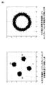
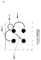
- FIG. 1 is a diagram showing four QPSK symbols and a bit string assigned thereto on a phase plane, which is called a QPSK constellation.
- associating a bit string with each symbol in the optical phase modulation method is called symbol mapping.
- QPSK is used as an optical phase modulation method
- the signal light and laser light (referred to as local light or local light) having substantially the same optical frequency as the signal light are combined by an optical element called a 90-degree hybrid.
- the output is received by an optical detector and converted into an electrical signal.
- Such a method is called an optical coherent method. For simplicity, it is assumed that the polarization states of the signal light and the local light are the same linearly polarized light.
- the AC component of the electrical signal output from the optical detector is a beat signal of signal light and local light.
- the amplitude is proportional to the amplitude of the signal light and the local light
- the phase is the difference between the optical phase of the signal light and the local light if the carrier frequency of the signal light and the optical frequency of the local light are the same.
- the optical phase of the local light is the same as the optical phase of the laser light input to the optical modulator at the transmitting end
- the phase of the beat signal is the optical phase imparted to the laser light at the transmitting end. Therefore, it is possible to demodulate transmission data by converting the phase of the beat signal into a bit string using symbol mapping. That is, if an optical signal having the constellation of FIG.
- the optical receiver can receive a signal having the same constellation.
- the carrier frequency of the signal light and the value of the optical frequency of the local light do not completely match, and the optical phase of the local light at the receiver and the optical phase of the laser light input to the optical modulator at the optical transmitter It does not match.
- the optical phase difference between the signal light and the local light input to the optical modulator is called an optical phase deviation
- the difference between the carrier frequency of the signal light and the optical frequency of the local light is called an optical carrier frequency deviation.
- the phase of the beat signal is a value obtained by adding the optical phase deviation to the product of the optical carrier frequency deviation and the reception time. Therefore, as shown in FIG. 2B, a signal having a constellation in which the constellation shown in FIG. 1 rotates in time is received. At this time, since the phase of the beat signal changes with time, it is impossible to demodulate data from the phase of the beat signal using the symbol mapping shown in FIG.
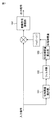
- FIG. 3 is a diagram showing the configuration of an optical phase deviation / optical carrier frequency deviation compensation circuit (hereinafter sometimes simply referred to as a compensation circuit).
- 3A is called a feed-forward type
- FIG. 3B is called a feedback type.
- FIG. 3A is called a feed-forward type
- FIG. 3B is called a feedback type.
- a circuit for estimating the phase compensation amount includes a phase error detection unit 101, a filter unit 102, and a phase compensation amount calculation unit 103.
- the phase error detection unit 101 is a circuit that detects a change in the optical phase deviation per unit time, that is, a change in the optical phase deviation between two adjacent symbols, and is an M-th Power Algorithm (Mth power) shown in FIG. Circuit) is widely used.
- the phase error detection unit 101 is a circuit that calculates the optical carrier frequency deviation.
- the output of the phase error detection unit 101 is sent to the filter unit 102 where the noise component is removed.
- the output of the filter unit 102 is sent to the phase compensation amount calculation unit 103 to calculate the actual phase compensation amount, that is, the rotation amount of the constellation.
- the phase compensation amount calculation unit 103 is equivalent to a circuit that is integrated and held.
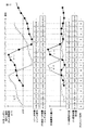
- FIG. 4 is a diagram illustrating an example of a temporal change in the phase compensation amount estimated by the compensation circuit.
- the horizontal axis represents time (time), and the vertical axis represents the phase compensation amount.
- the time is the reciprocal of the symbol rate input to the compensation circuit. As shown in FIG. 4, in this case, it can be seen that the phase compensation amount changes continuously in time.
- transmission data is transmitted by preventing rotation of the constellation using the optical phase deviation / optical carrier frequency deviation compensation circuit shown in FIG. Demodulate. Since the circuit shown in FIG. 3 is generally executed by digital signal processing, the optical phase modulation method is sometimes called an optical digital coherent method.
- the optical phase modulation method is sometimes called an optical digital coherent method.
- a noise component of light for example, nonlinear noise such as impulse noise, phase noise accompanied by a sudden phase change, and ASE noise is added to the input signal
- the phase compensation amount is estimated as indicated by ⁇ -1 in FIG. The value may suddenly change discontinuously.
- ASE is an abbreviation for Amplified Spontaneous Emission. Therefore, even if the optical phase deviation / optical carrier frequency deviation compensation circuit shown in FIG. 3 is used, rotation of the constellation due to a sudden phase shift (cycle slip, hereinafter referred to as slip) cannot be prevented.
- the symbol mapping changes (rotates). If this phenomenon occurs once, in the above method, it is impossible to confirm that a slip has occurred, so that erroneous data is demodulated.
- a method called differential encoding is generally used. Differential coding is a coding method in which a bit string is associated with a transition between two adjacent symbols.
- FIG. 6 shows an example of a QPSK constellation to which differential encoding is applied.
- FIG. 6 is a block diagram showing a configuration of a compensation circuit in an optical communication system using differential encoding.
- 2A is the same as the compensation circuit shown in FIG. 2A except that a differential code demodulator 104 is added after the compensation circuit shown in FIG.
- the differential code demodulator 104 converts the transition between adjacent symbols into a predetermined bit string. At this time, even if the constellation rotates, since the bit string is associated with the transition between adjacent symbols, the transmission data can be demodulated without any problem. As described above, even when a slip occurs, transmission data can be correctly demodulated by applying differential encoding.
- Patent Document 1 describes a technique for providing a phase synchronization circuit having a wide frequency range capable of performing a pull-in operation and a slip detector suitable for this. This shortens the access time from the unlocked state until the signal at the designated recording position of the recording medium is read.
- Patent Document 1 is a phase difference (phase error) between a signal and a clock as a monitoring target. Therefore, it does not solve the problem when the constellation rotates. Further, the related technology described above has the following problems. Since differential encoding assigns a bit string to transitions between adjacent symbols, if an error occurs in one symbol, both the transition from the immediately preceding symbol and the transition to the immediately following symbol are erroneous. Will occur. As a result, when differential coding is used, there is a problem that the bit error rate (BER) increases compared to when differential coding is not used.
- BER bit error rate
- the optical SNR Signal-to-Noise Ratio
- 3 dB the optical SNR (Signal-to-Noise Ratio) necessary for obtaining the same transmission characteristics in the same optical communication system.
- This causes problems such as deterioration of transmission characteristics due to the nonlinear optical effect due to an increase in the light intensity of the optical signal, and reduction of the transmittable distance.
- the object of the present invention has been made in view of the problems of the related art described above. In other words, even when optical phase deviation / optical carrier frequency deviation compensation processing is implemented, phase compensation (optical phase deviation / optical carrier frequency deviation compensation) that corrects slip and corrects transmission data without degrading transmission characteristics. The purpose is to do.
- the phase deviation compensation circuit of the phase modulation signal demodulator of the present invention detects the occurrence of slip of the received signal from the change of the phase compensation amount made to the received signal by the phase deviation compensation means, and the phase of the received signal after the occurrence of the slip Correct the compensation amount.
- the phase deviation compensation method of the present invention detects the occurrence of slip of the received signal from the change in the phase compensation amount of the received signal, and corrects the phase compensation amount of the received signal after the occurrence of the slip.
- the phase compensation (optical phase deviation / optical phase) that can correct the slip and correct the transmission data without degrading the transmission characteristics. Carrier frequency deviation compensation).
- A It is an example of a QPSK constellation and symbol mapping.
- A It is a figure which shows an example of the constellation and symbol mapping of QPSK rotated by the optical phase deviation.
- B It is a figure which shows an example of the constellation and symbol mapping of QPSK rotated continuously by the optical carrier frequency deviation.
- A It is a block diagram which shows the structure of a feedforward type optical phase deviation and optical carrier frequency deviation compensation circuit.
- B It is a block diagram which shows the structure of a feedback type optical phase deviation and optical carrier frequency deviation compensation circuit. It is a figure which shows the time change of the estimated value of a phase compensation amount. It is a figure which shows the time change of the estimated value of the phase compensation amount by noise.
- FIG. 1 is a block diagram illustrating a configuration of a compensation circuit unit (optical phase deviation / optical carrier frequency deviation compensation circuit) 201 according to a first embodiment.
- FIG. It is a block diagram which shows the structure of the compensation amount monitoring part 202 in 1st Embodiment.
- FIG. 3 is a block diagram illustrating a configuration of a compensation change amount comparison unit 303 in the first embodiment. It is a block diagram which shows the structure of the slip correction
- FIG. 3 is an example of a timing chart showing input / output timings of a symbol timing adjustment unit 304 and a delay unit 403 in the first embodiment. It is an example of the timing chart which shows the input / output timing of the correction amount calculation part 501 in 1st Embodiment. It is an example of the timing chart which shows the timing of the signal in the slip correction
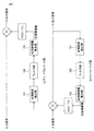
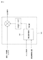
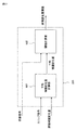
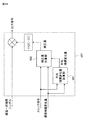
- FIG. 8 there is shown a block diagram showing a configuration of an optical phase deviation / optical carrier frequency deviation compensation circuit (hereinafter referred to as a slip compensation circuit) as a first embodiment of the present invention.
- the slip compensation circuit according to the first embodiment includes a compensation circuit unit 201, a compensation amount monitoring unit 202, a slip correction unit 203, and a compensation change amount threshold setting unit 204.
- the compensation circuit unit 201 outputs a signal obtained by compensating the phase of the input signal and the estimated compensation amount of the phase of the input signal to the compensation amount monitoring unit 202 as a primary compensation symbol signal and a compensation amount, respectively.
- FIG. 10 shows the configuration of the compensation circuit unit 201 shown in FIG. This circuit has basically the same configuration as the compensation circuit shown in FIG. 3A or FIG. 3B, but the phase compensation amount estimated by the compensation circuit as shown in FIG. The difference is that notification is possible.
- a compensation amount monitoring unit 202 shown in FIG. 8 monitors changes in the compensation amount input from the compensation circuit unit 201.
- the compensation amount monitoring unit 202 delays the slip signal indicating the occurrence location and the compensation change amount when a change exceeding the compensation change amount threshold value input from the compensation amount change amount threshold setting unit 204 occurs in the compensation amount.
- the delay compensation change amount is output to the slip correction unit 203.
- the compensation change amount threshold is a phase compensation change threshold. Referring to FIG. 11, details of the compensation amount monitoring unit 202 shown in FIG. 8 are shown.
- the compensation amount monitoring unit 202 includes a symbol time delay unit 301, a compensation change amount detection unit 302, a compensation change amount comparison unit 303, and a symbol timing adjustment unit 304.
- the symbol time delay unit 301 delays the compensation amount output from the compensation circuit unit 201 of FIG.
- the compensation change amount detection unit 302 receives the compensation amount output from the compensation circuit unit 201 in FIG. 8 and the compensation amount before J symbol time output from the symbol time delay unit 301 in FIG. 11. Thereafter, the compensation change amount detection unit 302 determines the difference between the compensation amount before J symbol time and the compensation amount output from the compensation circuit unit 201 in FIG. Output.
- the compensation change amount comparison unit 303 compares the compensation change amount output to the compensation change amount detection unit 302 with the compensation change amount threshold value output from the compensation change amount threshold setting unit 204, and compares the result with a slip signal and a delay.
- the compensation change amount is output to the slip correction unit 203.
- the symbol timing adjustment unit 304 performs primary compensation in order to match the timing of the primary compensation symbol output from the compensation circuit unit 201 of FIG. 8 with the slip signal and delay compensation change amount output from the compensation change amount comparison unit 303. Adjust symbol delay. After that, the symbol timing adjustment unit 304 outputs the delay-adjusted primary compensation symbol to the slip correction unit 203.
- FIG. 12 details of the compensation change amount comparison unit 303 shown in FIG. 11 are shown.
- the reason why the accumulating unit 401 is provided is as follows. That is, the amount of change in compensation caused by a slip that actually occurs in one symbol time is not always sufficiently large. Therefore, the occurrence of slip can be detected more reliably by adding (integrating) the compensation change amount over a plurality of symbols.
- the comparison unit 402 compares the accumulated compensation change amount input from the accumulation unit 401 with the compensation change amount threshold value input from the compensation amount change threshold setting unit 204, and uses the result as a slip signal to the slip correction unit 203. Output.
- the value of the slip signal is “1” when a slip occurs, and “0” otherwise.
- the delay unit 403 delays the compensation change amount input from the compensation change amount detection unit 302 by L symbol time (L is a positive integer), and outputs the delay change amount to the slip correction unit 203 as a delay compensation change amount.
- the slip correction unit 203 shown in FIG. 8 corrects the phase of the delayed primary compensation symbol output from the compensation amount monitoring unit 202 using the slip signal output from the compensation amount monitoring unit 202 and the compensation change amount. To do. Referring to FIG. 13, details of the slip correction unit 203 shown in FIG. 8 are shown.
- the correction amount calculation unit 501 calculates and outputs a correction amount from the delay compensation change amount and the slip signal output from the compensation amount monitoring unit 202.
- the correction amount calculated by the correction amount calculation unit 501 is a product of a complex number (expressed as exp ( ⁇ i ⁇ ) where the phase compensation amount is ⁇ ) and the input signal is output as an output signal. (Operation)
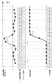
- FIG. 14 is a timing chart of the compensation circuit unit 201 shown in FIG. 8. Input signals S (0) to S (16) of the compensation circuit unit 201 shown in FIG.
- the symbol m changes from the symbol m to the symbol m + 16 in the portion ⁇ 1 where the compensation amount has changed.
- (b) primary compensation symbol signals H (0) to H (16) and (c) compensation amount signals ⁇ (0) to ⁇ (16) are outputs of the compensation circuit unit 201.
- ⁇ -3 in FIG. 14 represents the phase compensation amount ⁇ output from the compensation circuit unit 201
- ⁇ -2 in the figure represents the compensation amount ⁇ (0) at time 0T.
- ⁇ -4 in the figure indicates the compensation amount ⁇ when no slip occurs, and the slip compensation circuit in the first embodiment corrects the ⁇ -3 compensation amount to ⁇ -4.
- 0T to 16T indicate the time from the symbol m shown in FIG.
- the compensation circuit unit 201 in FIG. 8 estimates the phase compensation amount and the estimated phase as described in the related art section. Compensation of the input signal by the compensation amount is executed. At this time, the compensation circuit unit 201 outputs the estimated phase compensation amount ⁇ (1) and the primary compensation symbol signal H (1) compensated for the phase of the input signal to the compensation amount monitoring unit 202 at time 1T.
- the operation of the compensation amount monitoring unit 202 of FIG. 8 will be described using the configuration diagram shown in FIG. 11 and the timing chart shown in FIG. FIG. 15 is a timing chart of the symbol time delay unit 301 and the compensation change amount detection unit 302 shown in FIG.
- the compensation amount signals ⁇ (0) to ⁇ (16) in FIG. 15A are output signals from the compensation circuit unit 201.
- (b) delay compensation amount signals ⁇ ( ⁇ 1) to ⁇ (15) in the figure are output signals of the symbol time delay unit 301 in FIG. 11, and
- (c) compensation change amount signal D (0) ⁇ in FIG. D (16) is the output of the compensation change amount detection unit 302.
- graph ⁇ -3 shows (a) compensation amount signal ⁇
- graph ⁇ -5 shows (b) delay compensation amount signal ⁇
- graph ⁇ -6 shows (c) compensation change amount signal. Show.
- FIG. 15 when (i) the compensation amount ⁇ (1) in the figure is given to the symbol time delay unit 301 shown in FIG.
- the symbol time delay unit 301 receives J (J is 1 or more).
- the symbol time compensation amount ⁇ (1) is delayed as a positive integer (1 in this embodiment).
- the symbol time delay unit 301 outputs the signal as the delay compensation amount signal ⁇ (1) at time 2T to the compensation change amount detection unit 302 shown in FIG.
- (a) compensation amount ⁇ (2) and (b) delay compensation amount signal ⁇ (1) in the figure are provided to the compensation change amount detection unit 302 shown in FIG.
- compensation change amount detection section 302 obtains the difference between ⁇ (1) and ⁇ (2), and outputs compensation change amount D (3) to compensation change amount comparison section 303 shown in FIG. 11 at time 3T.
- the compensation change amount signals D (0) to D (16) in FIG. 16 are output signals from the compensation change amount detection unit 302. Also, (b) compensation change amount accumulation values A (0) to A (16) in the figure are output signals of the accumulation unit 401 in FIG. 12, and (c) compensation change amount threshold signal Th in the figure is shown in FIG. This is an output of the compensation change amount threshold setting unit 204. Further, the slip signal (D) in the figure is the output of the comparison unit 402 in FIG. In FIG.
- a graph ⁇ -6 indicates (a) a compensation change amount signal
- a graph ⁇ -7 indicates (b) a compensation change amount accumulated value
- a graph ⁇ -8 indicates (c) a compensation change amount threshold signal.
- the accumulation unit 401 adds the compensation change amount for K symbol time.
- the absolute value is output as a compensation change amount accumulated value A (4) at time 4T to the comparison unit 402 shown in FIG.
- the compensation change amount accumulated value A (4) at time 4T is the absolute value of the sum of the compensation change amounts D (2) and D (3), that is, A (4).
- compensation change accumulated value A (4) and (c) compensation change amount threshold signal Th in FIG. 16 are given to comparison unit 402 shown in FIG. Compares the compensation change amount accumulated value A (4) with the compensation change amount threshold signal Th. Thereafter, when the compensation change amount accumulated value A (4) is less than the compensation change amount threshold signal Th, the comparison unit 402 generates a slip signal ⁇ -8 having a value of 0 indicating that slip does not occur at time 5T and the slip correction of FIG. The data is output to the unit 203.
- the compensation change amount signals D (0) to D (16) of the primary compensation symbol signals H (0) to H (16) and (c) in FIG. 17A are output signals of the compensation circuit unit 201 in FIG. .
- (b) delayed primary compensation symbol signals H ( ⁇ 4) to H (13) in FIG. 17 are output signals of the symbol timing adjustment unit 304 in FIG. 11, and (d) delay compensation change amount D in FIG. ( ⁇ 3) to D (14) are outputs of the delay unit 403 in FIG.
- the slip signal (e) in FIG. 17 is the output of the comparison unit 402 in FIG.
- a graph ⁇ -3 shows (a) a primary compensation symbol signal
- a graph ⁇ -10 shows (b) a delayed primary compensation symbol signal
- a graph ⁇ -6 shows (c) a compensation change amount signal.
- the graph ⁇ -11 shows the (d) delay compensation change amount signal.
- the symbol timing adjustment unit 304 delays the primary compensation symbol signal H (0) in accordance with the processing delay of the slip signal in (e) in the figure, and displays the delayed primary compensation symbol signal H (0) at time 4T. 8 to the slip correction unit 203.
- the delay unit 403 processes the slip signal in FIG. Accordingly, the compensation change amount D (1) is delayed. Thereafter, the delay unit 403 outputs the delay compensation change amount D (1) to the slip correction unit 203 in FIG. 8 at time 4T.
- the slip compensation signals D (0) to D (16) and (b) in FIG. 18 (a) are output signals of the compensation amount monitoring unit 202 in FIG.
- correction amounts B (3) to B (19) in FIG. 18 are output signals of the correction amount calculation unit 501 in FIG.
- a graph ⁇ -11 in FIG. 18 indicates (a) a delay compensation change amount
- a graph ⁇ -12 indicates (c) a correction amount. 18, the delay compensation change amount and the slip signal are given to the correction amount calculation unit 501 in FIG.
- the correction amount calculation unit 501 adds the delay compensation change amount and the correction amount one symbol time ago, and uses the addition result as the correction amount. Output.
- the value of the slip signal is “0” indicating that no phase slip has occurred, the delay compensation change amount and the correction amount are not added, and the correction amount one symbol time before is output.
- the delay compensation change amount D (1) in FIG. 18 (a) and the slip signal ⁇ -13 in (b) are given to the correction amount calculation unit 501 in FIG. In the quantity calculation unit 501, the value of the slip signal ⁇ -13 is “0”.
- correction amount B (4) is output as the correction amount B (5) at time 5T.
- the correction amount calculation unit 501 when the delay compensation change amount D (7) in FIG. 18 (a) and the slip signal ⁇ -14 in (b) are given to the correction amount calculation unit 501 in FIG. 13, the correction amount calculation unit 501.
- the value of the slip signal ⁇ -14 is “1”. Therefore, at time 11T, the sum of the correction amount B (10) and the delay compensation change amount D (7) is output as the correction amount B (11).
- the initial value of the correction amount B is “0”, but is not particularly limited thereto.
- Correction amounts B (3) to (19) shown in FIG. 19 are output signals of the correction amount calculation unit 501 in FIG.
- (b) delayed primary compensation symbol signals H ( ⁇ 1) to H (15) in FIG. 19 are output signals of the compensation amount monitoring unit 202 in FIG.
- (c) correction symbol signals C (3) to C (19) are correction symbol signals subjected to phase correction and output from the slip correction unit 203.
- a graph ⁇ -12 indicates (a) the correction amount
- a graph ⁇ -10 indicates (b) the compensation amount applied to the primary compensation symbol signal
- a graph ⁇ -15 indicates (c) the correction symbol.
- the correction amount in FIG. 17A output from the correction amount calculation unit 501 in FIG. 13 is a complex number (expressed as exp ( ⁇ iB) where B is the phase correction amount), and (B) delay in the figure.
- the product with the primary compensation symbol signal is output as a corrected symbol signal. That is, the compensation amount ⁇ applied to the delayed primary symbol signal H (7) and the compensation amount B (11) are added at time 11T, and the phase-corrected compensation symbol C (12) is output at time 12T. To do. In FIG. 19, the correction amount is applied after ⁇ -16.
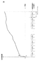
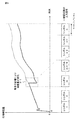
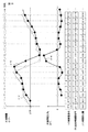
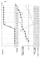
- FIG. 26 is a diagram illustrating a phase compensation amount after correction when actual measurement data is corrected based on the first embodiment. As described above, in the above embodiment, the phase compensation amount from the compensation circuit unit 201 is monitored by the compensation amount monitoring unit 202. Therefore, when a slip occurs, the change in the phase compensation amount due to the slip is corrected by the slip correction unit. I can do it.
- an accumulation unit 401 that accumulates the compensation change amount for K symbol time is provided in the compensation amount monitoring unit 202. Therefore, even when a slip occurs over a plurality of symbol times, an abnormal change in compensation amount due to the slip can be detected, and the abnormal compensation amount can be corrected by the slip correction unit 203.
- the signal compensated by 4) can be output.
- the change in the compensation amount is monitored in order to identify the slip occurrence location.
- the compensation circuit unit 201 may be used instead of the change in the compensation amount.
- the change in the output signal of the filter unit 102 may be used together with the change in the compensation amount.
- the phase compensation amount is reflected in the input signal in the compensation circuit unit, and the data is output to the subsequent stage.
- the slip compensation unit 203 applies the compensation amount finally slip cancelled. May be.
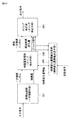
- the basic configuration is as described above, but the generation of the compensation change amount threshold is further devised. The configuration is shown in FIG. In FIG. 8, the compensation circuit unit 201, the compensation amount monitoring unit 202, and the slip correction unit 203 are the same as those in FIG.
- the compensation change amount threshold value determination unit 205 determines a compensation change amount threshold value used to detect the occurrence of slip. Referring to FIG. 21, the configuration of the compensation change amount threshold value determination unit 205 shown in FIG. 20 is shown.
- the compensation change threshold determination unit 205 includes an average change calculation unit 601 and a threshold calculation unit 602.
- the average change amount calculation unit 601 calculates a moving average of the delay compensation change amount, and outputs the calculation result to the threshold value determination unit 602.
- the threshold determination unit 602 calculates a compensation change amount threshold based on the average compensation change amount.
- the compensation change amount threshold value is calculated from the average compensation change amount and the coefficient signal, and is output to the compensation amount monitoring unit 202.
- the coefficient signal is connected to a control unit such as a CPU. (Operation) 21 is supplied from the compensation amount monitoring unit 202 with the delay compensation variation amount and the slip signal. Then, only when the value of the slip signal is “0”, the average change amount calculation unit 601 calculates the moving average of the delay compensation change amount of the W symbol time, and determines the threshold value using the calculation result as the average compensation change amount V. To the unit 602. Since the moving average is calculated only when the value of the slip signal is “0”, the average compensation change amount does not include the compensation amount when the slip occurs.
- the average compensation change amount V is given to the threshold value determination unit 602 from the average compensation change amount calculation unit 601. Then, the threshold value determination unit 602 outputs, to the compensation amount monitoring unit 202, a value obtained by multiplying the average compensation change amount by K and further multiplying the coefficient signal ⁇ as a compensation change amount threshold value th as shown in Expression (1) as an example.
- K is the accumulated symbol time of the accumulating unit 401 shown in FIG. 12, and the coefficient signal ⁇ indicates the deviation rate from the moving average. This coefficient signal ⁇ is set in order to appropriately adjust the value of the compensation change amount threshold th.
- Compensation change threshold th average compensation change V ⁇ K ⁇ ⁇ (1)
- the compensation circuit unit 201, the compensation amount monitoring unit 202, and the slip correction unit 203 other than those described above perform the same operations as in the first embodiment.
- the compensation change threshold value used to detect the occurrence of slip is generated from the delay compensation change amount and the slip signal. Therefore, even when the compensation change amount changes, an appropriate compensation change amount threshold value can be obtained. For this reason, the effect of suppressing errors due to correction errors can be obtained.
- the basic configuration is as described above, but the generation of the compensation change amount threshold is further devised. The configuration is shown in FIG. In this figure, the configuration is the same as that of the second embodiment shown in FIG.
- a synchronization pattern insertion unit 701, a modulation unit 702, and a synchronization unit 206 are added to the configuration of the second embodiment shown in FIG. .
- the synchronization pattern insertion unit 701 and the modulation unit 702 are arranged on the transmission side and are not shown, an SD-FEC encoding unit and a framer unit are arranged on the input side of the synchronization pattern insertion unit.
- the synchronization pattern insertion unit 701 inserts a synchronization pattern into the output data from the SD-FEC encoding unit, and outputs it to the modulation unit 702.
- Modulation section 702 modulates the data input from the synchronization pattern and transmits it to the receiving side.
- QPSK will be described as an example of the modulation method, but the present invention is not limited to this.
- a circuit for demodulating a received signal is disposed between the modulation unit 702 and the compensation circuit unit 201, although not shown.
- the synchronization unit 206 is connected to the slip correction unit 203, the compensation amount monitoring unit 202, and the compensation change amount determination unit 205, detects a synchronization pattern from the correction symbol signal, and checks the normality of the phase of the correction symbol signal. Further, when a synchronization loss occurs after detection of the synchronization pattern, the phase amount of the correction symbol signal is corrected again according to the state of the slip signal.
- FIG. 23 is a diagram illustrating an input signal and an output signal of the synchronization pattern insertion unit 701 arranged on the transmission side.
- the input signal of the synchronous pattern insertion unit 701 in (a) is framed every y bits by the framer unit, and includes the parity calculated by the SD-FEC encoding unit.
- UW Unique Word
- DATA user data
- P is a parity value calculated by the SD-FEC encoding unit.
- the y bit is described as 32768 bits (4096 bytes) as an example.
- the output signal of the synchronization pattern insertion unit 701 in (b) is output with a 2-bit width of I and Q. This is because the modulation scheme in the modulation unit 702 is QPSK.
- the pattern to be inserted by the synchronization pattern insertion unit is inserted according to the following conditions.
- Condition 1 When the head data is UW, “0” is set to I and “1” is set to Q as the synchronization pattern ⁇ -20. In other cases, “1” is set to I and “0” is set to Q as the synchronization pattern ⁇ -21.
- the synchronization pattern insertion unit 701 separates the input signal from the UW every x bits, and the condition 1 is set every x bits. A corresponding synchronization pattern is inserted and output to modulation section 702.
- x is a positive integer and a divisor of y, and in the present embodiment, x bits are assumed to be 64 bits.
- the modulation unit 702 modulates the input I and Q and transmits them to the reception side.
- the received signal is placed at a location indicated by ⁇ -20 or ⁇ -21 shown in FIG. 1 every 32 (x bits / 2) symbol time.
- a synchronization pattern appears.
- a synchronization pattern appears at a location indicated by ⁇ -20 every 256 (y / x / 2) symbol time.
- I ′ and Q ′ in (A) are diagrams showing the correction symbol signal output from the slip correction unit 203 as a complex number.
- the synchronization signals in (b) in both figures indicate the synchronization state in the synchronization unit 206, and out-of-synchronization occurs at ⁇ -18.
- C) in both figures is a slip signal output from the compensation amount monitoring unit 202.
- D) in both figures are the re-corrected symbol signals 1 ′′ and Q ′′ output from the synchronization unit 206.
- the coefficient signal ⁇ in (e) is a signal output from the synchronization unit 206 to the compensation change threshold determination unit 205, and is used to calculate the compensation change threshold.
- FIG. 24 is a diagram when a correction error occurs due to the correction of the slip correction unit 203, and ⁇ -17 indicates the position of the correction error.
- FIG. 25 is a diagram in the case where the slip correction unit 203 cannot complete the correction, and a slip occurs at some point after ⁇ -21 in FIG.
- the synchronization unit 206 is inserted from the correction symbol signal (I ′, Q ′) by the synchronization pattern insertion unit 701.
- a synchronization pattern is detected, and a synchronization signal shown in FIG.
- the synchronization unit 206 re-corrects the correction symbol signal from a point ⁇ -22 where the value of the slip signal immediately before the loss of synchronization is “1”.
- the correction amount can be a difference from the synchronization pattern. Further, by increasing the slip signal generation threshold, it is possible to prevent a correction error that occurs because the slip signal generation threshold is not appropriate.
- the value of the coefficient signal ⁇ that is a coefficient of the threshold value for generating the slip signal is increased so as to satisfy ⁇ (r ⁇ 1) ⁇ (r), and is output to the compensation change amount threshold value determination unit.
- ⁇ is a coefficient of the threshold value for generating the slip signal.
- the synchronization unit 206 is inserted from the correction symbol signal (I ′, Q ′) by the synchronization pattern insertion unit 701.
- a synchronization pattern is detected, and a synchronization signal shown in FIG. In FIG. 25, loss of synchronization occurs at ⁇ -18.
- the slip signal shown in FIG. 25C is “0”
- the correction symbol signal is corrected again.
- the value of the slip signal is “0”, the location where the slip occurs is unknown, and it is necessary to determine the recorrection location of the slip.
- the synchronization unit 206 decreases the value of the coefficient signal ⁇ , which is a slip signal generation threshold coefficient, such that ⁇ (u ⁇ 1)> ⁇ (u), and the compensation change amount threshold determination unit. Output to.
- the synchronization pattern is inserted by the synchronization pattern insertion unit 701 on the transmission side, and detected by the synchronization unit 206, thereby controlling the compensation change amount threshold used for detecting the occurrence of slip. ing. Specifically, the coefficient signal ⁇ of the compensation change amount threshold value is generated. As a result, erroneous detection of slip can be suppressed, and the effect of improving transmission characteristics can be obtained.
- the effect of improving the transmission characteristics can be obtained.
- the first effect is that the transmission characteristics of the optical communication system can be improved by 3 dB. The reason is that it is possible to correct the mapping deviation due to slip without using differential encoding.
- the second effect can improve the transmission characteristics of the optical communication system. The reason is that, since differential coding is not used, the calculation of SD-FEC LLR that can be expected to have a high error correction gain can be realized without adding complicated processing.
- the third effect is that the transmission characteristics of the optical communication system can be improved. This is because the influence of slip can be suppressed within the synchronization patterns by detecting the synchronization pattern inserted in the signal on the transmission side on the transmission side. That is, an error larger than the synchronization pattern interval does not occur.
- the fourth effect is that the transmission characteristics of the optical communication system can be improved. The reason is that the transmitting side detects the synchronization pattern inserted in the signal on the receiving side, and changes the compensation change amount threshold value, which is the slip detection threshold value, to an appropriate value according to the number of slips generated between the synchronization patterns. be able to. This is because errors due to slip can be suppressed. (Fourth embodiment) A fourth embodiment of the present invention will be described with reference to FIG.
- the phase deviation compensation circuit 2701 of the phase modulation signal demodulator of this embodiment detects the occurrence of slip of the reception signal from the change in the amount of phase compensation made to the reception signal by the phase deviation compensation circuit, and the reception signal after the occurrence of the slip. The phase compensation amount is corrected.
- the phase deviation compensation circuit of the phase modulation signal demodulator of this embodiment has the following effects. In other words, even when optical phase deviation / optical carrier frequency deviation compensation processing is implemented, a slip compensation method (optical phase deviation / optical carrier frequency deviation compensation method) that can correctly demodulate transmission data without degrading transmission characteristics is provided. it can.
- the basic configuration is the same as that of the first embodiment, but the correction amount generation is further devised.
- the configuration is the same as that of the first embodiment shown in FIG. 8 except that the slip correction unit 203 shown in FIG. 8 is changed to a slip correction unit 207.
- the slip correction unit 207 is the same block as the slip correction unit 203 except that the “average compensation change amount” is applied to the correction amount calculated in the slip correction unit 203.
- FIG. 28 the configuration of the slip correction unit 207 shown in the figure is shown.
- the average compensation change amount calculation unit 601 calculates a moving average of the delay compensation change amount and outputs it to the correction amount calculation unit 502.
- the correction amount calculation unit 502 calculates and outputs a correction amount from the delay compensation change amount output from the compensation amount monitoring unit 202, the slip signal, and the average compensation change amount from the average compensation change amount calculation unit 601.
- the correction amount calculated by the correction amount calculation unit 502 is a product of a complex number (expressed as exp ( ⁇ i ⁇ ) where the phase compensation amount is ⁇ ) and the input signal is output as an output signal. (Operation) 28, the compensation amount monitoring unit 202 gives the delay compensation change amount and slip signal, and the average compensation change amount calculation unit 601 gives the average compensation change amount.
- FIG. 29 is a diagram illustrating an output signal of the correction amount calculation unit 502 of the present embodiment.
- (A) Delayed primary compensation symbol signals H ( ⁇ 1) to H (15) illustrated in FIG. 29 are illustrated in FIG. This is an output signal of the compensation amount monitoring unit 202.
- (b) correction symbol signals C (3) to C (19) are phase-corrected symbol signals output from the slip correction unit 207.
- the graph ⁇ -10 in the figure shows the compensation amount applied to the primary compensation symbol signal of (A).
- the graph ⁇ -15 indicates the phase correction amount applied to the correction symbol signal in the first embodiment
- the graph ⁇ -17 indicates the correction amount applied to the correction signal in the present embodiment.
- the correction value generated by the above equation (2) is applied.
- the compensation circuit unit 201, the compensation amount monitoring unit 202, the compensation change amount threshold setting unit 204 performs the same operation as in the first embodiment, and the average compensation change amount calculation unit 601 performs the second implementation.
- the same operation as that of the form is performed.
- the present embodiment differs from the first embodiment in that the correction amount for canceling the compensation amount when the slip occurs is generated, but the following points are different. That is, in order to add the average compensation change amount to the canceled compensation amount, a correction amount that takes into account the change amount that should be increased (or decreased) when a slip occurs is generated. For this reason, the effect of suppressing the phase shift due to the occurrence of slip is obtained.
- a dedicated device is assumed, but the following may be used. That is, for example, a personal computer device that performs various data processing is loaded with a board or a card that performs processing corresponding to this example, and each processing is executed on the computer device side. In this way, a configuration may be adopted in which software for executing the processing is installed in a personal computer device and executed.
- the program installed in the data processing device such as the personal computer device may be distributed via various recording (storage) media such as an optical disk and a memory card. Or you may distribute via communication means, such as the internet.
- each of the above embodiments can be combined with other embodiments. While the present invention has been described with reference to the embodiments, the present invention is not limited to the above embodiments.
- a phase modulation signal demodulator characterized by detecting the occurrence of slip of a received signal from a change in the amount of phase compensation applied to the received signal by a phase deviation compensation means and correcting the phase compensation amount of the received signal after the occurrence of the slip Phase deviation compensation circuit.
- Phase compensation means for compensating the phase deviation for the input signal
- Slip detection means for monitoring the change of the phase compensation amount in the phase compensation means and detecting the occurrence of slip
- Slip correction means for correcting a phase change caused by the slip detected by the slip detection means
- a phase deviation compensation circuit for a phase modulation signal demodulator.
- the phase deviation compensation circuit for a phase modulation signal demodulator according to appendix 2 wherein (Appendix 4) The threshold is determined based on a moving average of the amount of change in the phase compensation
- the phase deviation compensation circuit also includes carrier frequency deviation compensation.
- (Appendix 11) Compensate the phase deviation for the input signal, Monitors changes in phase compensation and detects slip occurrence. Compensate for phase change caused by slip
- a phase deviation compensation method characterized by the above. (Appendix 12) The detection of the slip is detected when the amount of change in phase compensation exceeds a predetermined threshold.
- the phase deviation compensation method according to appendix 12, wherein: (Appendix 14) Detect a synchronization pattern inserted in the received signal, and recorrect the phase compensation amount.
- the phase deviation compensation method according to any one of Supplementary Note 10 to Supplementary Note 13, wherein (Appendix 15) 15.
- phase deviation compensation method wherein the synchronization pattern has different patterns at the beginning of the frame and other positions.
- Appendix 16 A phase compensation process for compensating the phase deviation for the input signal; A slip detection process for detecting the occurrence of slip by monitoring a change in the amount of phase compensation in the phase compensation process; A slip correction process for correcting a phase change caused by the slip detected in the slip detection process; A phase deviation compensation program for causing a computer to execute the above.
- the present invention relates to a receiver that performs frequency phase deviation / carrier frequency deviation compensation, and more particularly to optical phase deviation / optical carrier frequency deviation compensation when a cycle (phase) slip occurs, and has industrial applicability. .
Landscapes
- Engineering & Computer Science (AREA)
- Computer Networks & Wireless Communication (AREA)
- Signal Processing (AREA)
- Physics & Mathematics (AREA)
- Electromagnetism (AREA)
- Digital Transmission Methods That Use Modulated Carrier Waves (AREA)
- Synchronisation In Digital Transmission Systems (AREA)
Abstract
Description
超高速の光通信システムを実現する技術として、近年光位相変調方式が注目されている。光位相変調方式は関連の光強度変調方式のように送信レーザ光の光強度に対してデータ変調を行うのではなく、送信レーザ光の位相に対してデータ変調を行う方式でありQPSKや8PSKなどの方式が知られている。なおQPSKはQuadrature Phase Shift Keying、8PSKは8 Phase Shift Keyingの略語である。
光位相変調方式の利点は次の通りである。即ち1シンボルに対して複数のビットを割り当てることにより、シンボルレート(ボーレート)を低下させることが可能なので、電気デバイスの動作速度を低減できる。その結果、装置の製造コストの削減が期待できることにある。例えば、QPSKを用いる場合、4個の光位相(例えば45度、135度、225度、315度)に対して、それぞれ2ビット(例えば00、01、11、10)を割り当てる。そのためQPSKのシンボルレートは光強度変調方式のシンボルレート(すなわちビットレート)の1/2に低減できる。
図1は、QPSKの4個のシンボルとそれに割り当てられたビット列を位相平面上に示した図であり、QPSKのコンスタレーションと呼ばれる。また光位相変調方式における各シンボルにビット列を対応付けることをシンボルマッピングと呼ぶ。以降では光位相変調方式としてQPSKを用いた場合を例として説明するものとするが、他の光位相変調方式も適用可能である。
光位相変調された信号光を受信するためには、信号光と、信号光とほぼ同一の光周波数を有するレーザ光(局所光又はローカル光と呼ばれる)を90度ハイブリッドと呼ばれる光学素子により結合する。その後、その出力を光ディテクタにより受光し電気信号に変換した信号とする。この様な方式は光コヒーレント方式と呼ばれる。
簡単のため信号光と局所光の偏波状態は同一の直線偏光であると仮定する。光コヒーレント方式を用いた場合、光ディテクタから出力される電気信号の交流成分は信号光と局所光のビート信号である。その振幅は信号光と局所光の振幅に比例し、その位相は、信号光の搬送波周波数と局所光の光周波数が同一であれば、信号光と局所光の光位相の差となる。局所光の光位相が送信端の光変調器に入力されるレーザ光の光位相と同一であれば、ビート信号の位相が送信端でレーザ光に付与された光位相である。そのため、シンボルマッピングを用いてビート信号の位相をビット列に変換することにより送信データを復調することが可能である。すなわち、光送信機から図1のコンスタレーションを有する光信号を送信すれば、光受信機では同様のコンスタレーションを有する信号を受信することができる。
しかし一般に信号光の搬送波周波数と局所光の光周波数の値は完全に一致しない上に、受信機における局所光の光位相と、光送信機において光変調器に入力されるレーザ光の光位相も一致しない。
光送信機において光変調器に入力される信号光と局所光の光位相差は光位相偏差、信号光の搬送波周波数と局所光の光周波数の差は光搬送波周波数偏差と呼ばれる。光位相偏差が存在する場合、図2(a)に示すように、図1に示すコンスタレーションに対して光位相偏差だけ回転したコンスタレーションを有する信号が受信される。光位相偏差の値は予め知ることができないため、図1に示すシンボルマッピングをそのまま用いて、シンボルをビット列に変換すると誤ったデータが復調されてしまうという問題が生じる。
さらに、光搬送波周波数偏差が存在する場合、前述のビート信号の位相は光搬送波周波数偏差と受信時刻の積に光位相偏差を加えた値となる。そのため、図2(b)に示すように、図1に示すコンスタレーションが時間的に回転するコンスタレーションを有する信号が受信される。このときビート信号の位相は時間的に変化するため、図1に示すシンボルマッピングを用いてビート信号の位相からデータを復調することは不可能である。
従って、光位相変調方式においては、光位相偏差と光搬送波周波数偏差によるコンスタレーションの回転を防止する光位相偏差・光搬送波周波数偏差補償機能が必要となる。以降では、光位相変調方式で広く用いられている光位相偏差・光搬送波周波数偏差補償処理を説明する。
図3はいずれも光位相偏差・光搬送波周波数偏差補償回路(以降では単に補償回路と記述することがある)の構成を示す図である。図3(a)はフィードフォワード型、図3(b)はフィードバック型と呼ばれる。以降では図3(a)に示すフィードフォワード型についてのみ説明する。
補償回路の入力信号は2つに分岐されて、一方は位相補償量を推定する回路に入力され、他方は推定した位相補償量だけの逆回転を与える複素数との積を取った上で、補償後の信号として出力される。位相補償量を推定する回路は、位相誤差検出部101と、フィルタ部102と、位相補償量算出部103により構成される。位相誤差検出部101は光位相偏差の単位時間当たりの変化、すなわち隣り合う2個のシンボル間の光位相偏差の変化を検出する回路であって、図9に示すM−th Power Algorithm(M乗回路)が広く用いられている。
隣接する2個のシンボル間の光位相偏差の変化は、光搬送波角周波数偏差と1シンボル時間(1シンボル時間はシンボルレートの逆数に等しい)の積に等しく、また1シンボル時間は一定である。そのため、位相誤差検出部101は光搬送波周波数偏差を算出する回路であると言える。
位相誤差検出部101の出力はフィルタ部102に送られて、フィルタ部102において雑音成分が除去される。フィルタ部102の出力は位相補償量算出部103に送られて、実際の位相補償量、すなわちコンスタレーションの回転量が算出される。具体的には位相補償量算出部103は積分して保持する回路と等価である。
最後に位相補償量算出部103により算出された位相補償量だけの逆回転を与える複素数(位相補償量をφとするとexp(−iφ)で表される)と入力信号との積が出力信号として出力される。
図4は補償回路が推定した位相補償量の時間変化の一例を示す図である。横軸は時間(時刻)、縦軸は位相補償量を示す。時間は補償回路に入力されるシンボルレートの逆数となる。図4に示すように、この場合は位相補償量は時間的に連続的に変化することが分かる。
以上に説明したように、光位相変調方式を用いた光通信システムにおいては、図3に示す光位相偏差・光搬送波周波数偏差補償回路を用いてコンスタレーションの回転を防止することにより、送信データを復調する。図3に示す回路は一般にディジタル信号処理により実行されるため、光位相変調方式は光ディジタルコヒーレント方式と呼ばれることがある。
しかし上記方式を用いた超高速光通信システムの実現においては次の問題がある。即ち光の雑音成分、例えばインパルス雑音の様な非線形雑音、急激な位相変化を伴う位相雑音、およびASE雑音が入力信号に加わることにより、図5のα−1に示すように位相補償量の推定値が突発的に不連続に変化する場合がある。なおASEはAmplified Spontaneous Emissionの略語である。その為図3に示す光位相偏差・光搬送波周波数偏差補償回路を用いたとしても、位相の急激なズレによるコンスタレーションの回転(サイクルスリップ、以降スリップと記す。)を防止することができず、シンボルマッピングが変化(回転)してしまうことである。この現象が1度発生すると、上記の方式では、スリップが発生したことを確かめることができないため、誤ったデータが復調されることになる。
上述の問題を解決するために差動符号化と呼ばれる方法が一般に用いられる。差動符号化は隣り合う2個のシンボル間の遷移に対してビット列を対応付ける符号化方法である。
図6に差動符号化を適用したQPSKのコンスタレーションの一例を示す。差動符号化を用いる光通信システムにおいては、図6に示すように、シンボル自身にビット列が対応付けられるのではなく、あるシンボルから同一の又は他のシンボルへの遷移に対してビット列がマッピングされる。例えば、図6においては、隣り合うシンボル間の位相変化が+0度の遷移1に対して00、+90度の遷移2に対して01、+180度の遷移3に対して11、+270度の遷移4に対して10がそれぞれ割り当てられている。
図7は差動符号化を用いる光通信システムにおける補償回路の構成を示すブロック図である。図2(a)の補償回路の後段に差動符号復調部104が追加された点を除いて、図2(a)に示す補償回路と同一である。差動符号復調部104は前述したように隣り合うシンボル間の遷移を所定のビット列に変換する。このとき、コンスタレーションが回転したとしても、隣り合うシンボル間の遷移に対してビット列が対応付けられていることから、送信データは問題無く復調することが可能である。
以上に説明したように、スリップが発生した場合においても、差動符号化を適用することにより、送信データを正しく復調することが可能となっている。
関連する技術として、特許文献1には引き込み動作を行うことのできる周波数レンジの広い位相同期回路及びこれに好適なスリップ検出器を提供する技術が記載されている。これはアンロック状態から記録媒体の指定された記録位置の信号を読み取るまでのアクセス時間を短縮するというものである。
また、上述した関連の技術においては、以下に述べるような問題がある。
差動符号化は隣り合うシンボル間の遷移に対してビット列を割り当てるため、1個のシンボルに誤りが発生した場合、その直前のシンボルからの遷移と、その直後のシンボルへの遷移の両方に誤りが生じることになる。その結果、差動符号化を用いる場合は、差動符号化を用いない場合に比べて、ビット誤り率(BER:Bit Error Rate)が増大してしまうという問題がある。理論的には同一の光通信システムにおいて同一の伝送特性を得るために必要な光SNR(Signal−to−Noise Ratio)は差動符号化を用いる場合の方が3dB高くなる。このことは光信号の光強度の増大による非線形光学効果のために伝送特性の劣化を招いたり、伝送可能距離を短縮させたりするなどの問題を生じさせる。
(発明の目的)
本発明の目的は、上述の関連技術が有する問題を鑑みてなされたものである。即ち光位相偏差・光搬送波周波数偏差補償処理を実装する場合においても、伝送特性を低下させることなく、スリップを補正し送信データを正しく復調可能な位相補償(光位相偏差・光搬送波周波数偏差補償)を行うことを目的とする。
本発明の位相偏差補償方法は、受信信号の位相補償量の変化から、受信信号のスリップの発生を検出し、スリップ発生後の受信信号の位相補償量を補正する。
(第1の実施形態)
以下、本発明の第1の実施形態を図面を参照して説明する。
(構成)
図8を参照すると、本発明の第1の実施形態としての光位相偏差・光搬送波周波数偏差補償回路(以降スリップ補償回路と称す)の構成を示すブロック図が示されている。
図8に示すように、第1実施形態におけるスリップ補償回路は、補償回路部201と、補償量監視部202と、スリップ補正部203と、補償変化量閾値設定部204により構成される。
補償回路部201は、入力信号の位相を補償した信号と、推定された入力信号の位相の補償量を、それぞれ一次補償シンボル信号、および補償量として補償量監視部202へ出力する。
図10に図8に示される補償回路部201の構成を示す。この回路は、図3(a)または図3(b)に示す補償回路と基本的に同様の構成を有するが、図10に示すように補償回路が推定した位相補償量を他の機能ブロックに通知可能である点が異なる。
図8に示される補償量監視部202は、補償回路部201から入力した補償量の変化を監視する。補償量監視部202は、補償量変化量閾値設定部204から入力した補償変化量閾値を超えた変化が補償量に生じた場合、その発生箇所を示したスリップ信号と、補償変化量を遅延させた遅延補償変化量を、スリップ補正部203へ出力する。ここで補償変化量閾値とは位相の補償変化量の閾値である。
図11を参照すると、図8に示す補償量監視部202の詳細が示されている。補償量監視部202は、シンボル時間遅延部301、補償変化量検出部302、補償変化量比較部303、およびシンボルタイミング調整部304より構成される。
シンボル時間遅延部301は、図8の補償回路部201から出力された補償量を、Jシンボル時間(Jは、正の整数、本実施形態では、一例としてJ=1とする)遅延し、補償変化量検出部302へ出力する。
補償変化量検出部302は、図8の補償回路部201から出力された補償量と、図11のシンボル時間遅延部301から出力されるJシンボル時間前の補償量とを入力する。その後補償変化量検出部302は、Jシンボル時間前の補償量と図8の補償回路部201から出力された補償量との差を求めたものを補償変化量として、補償変化量比較部303へ出力する。
補償変化量比較部303は、補償変化量検出部302に出力された補償変化量と、補償変化量閾値設定部204から出力された補償変化量閾値を比較し、その結果をスリップ信号、および遅延補償変化量として、スリップ補正部203へ出力する。
シンボルタイミング調整部304は、補償変化量比較部303より出力されるスリップ信号と遅延補償変化量に、図8の補償回路部201から出力された一次補償シンボルのタイミングを一致させるために、一次補償シンボルの遅延調整を行う。その後シンボルタイミング調整部304は、遅延調整された一次補償シンボルをスリップ補正部203へ出力する。
図12を参照すると、図11に示す補償変化量比較部303の詳細が示される。
累積部401は、補償変化量検出部302から出力される補償変化量をKシンボル時間分(Kは正の整数、一例として本実施形態ではK=2)の加算を行い、補償変化量累積値として、比較部402へ出力する。この累積部401を設ける理由は以下の通りである。即ち、現実に1シンボル時間で生じるスリップに起因する補償変化量は必ずしも十分に大きいものであるとは限らない。従って、補償変化量を複数シンボルに跨って加算(積分)することでより確実にスリップ発生を検出できるようにしている。
比較部402は、累積部401から入力した補償変化量累積値と補償量変化量閾値設定部204から入力した補償変化量閾値との比較を行い、その結果をスリップ信号として、スリップ補正部203へ出力する。スリップ信号はスリップが発生した場合にその値が“1”、それ以外の場合は“0”になる。
遅延部403は、補償変化量検出部302から入力した補償変化量を、Lシンボル時間(Lは正の整数)遅延し、遅延補償変化量として、スリップ補正部203へ出力する。本実施形態では、補償変化量を、累積部の累積時間(前述のKシンボル時間)に合わせ遅延(L=Kシンボル時間遅延)させる。
図8に示されるスリップ補正部203は、補償量監視部202から出力されるスリップ信号、および補償変化量を用いて、前述の補償量監視部202から出力される遅延一次補償シンボルの位相を補正する。
図13を参照すると、図8に示すスリップ補正部203の詳細が示される。
補正量計算部501は、補償量監視部202から出力される遅延補償変化量とスリップ信号から、補正量を計算し、出力する。補正量計算部501により算出された補正量は、複素数(位相補償量をφとするとexp(−iφ)で表される)と入力信号との積が出力信号として出力される。
(動作)
次に図8、10、11、12、13に示す構成図、および図14、15、16、17、18、19に示すタイミングチャートを使用し、第1の実施形態におけるスリップ補償回路の動作を説明する。
図14は、図8に示す補償回路部201のタイミングチャートであり、図14(イ)の補償回路部201の入力信号S(0)~S(16)は、図5に示す雑音の影響により補償量が変化した箇所α−1の部分のシンボルmからシンボルm+16に一致する。図における(ロ)一次補償シンボル信号H(0)~H(16)、および(ハ)補償量信号φ(0)~φ(16)は、補償回路部201の出力である。
また、図14内α−3は、補償回路部201から出力される位相の補償量φを示し、図におけるα−2は、時刻0Tにおける補償量φ(0)を示す。図内α−4は、スリップが発生しない場合の補償量φを示しており、第1の実施形態におけるスリップ補償回路は、α−3補償量をα−4へ補正する。
なお、図内の0T~16Tは、図5に示すシンボルmからの時刻を示し、1Tは、1シンボル時間に相当する。
図8の補償回路部201は、図14(イ)の入力信号(シンボル)S(0)を時刻0Tに受け取ると、関連技術の項で述べた通り、位相補償量の推定と、推定した位相補償量による入力信号の補償を実行する。このとき補償回路部201は推定した位相の補償量φ(1)と、入力信号の位相を補償した一次補償シンボル信号H(1)を時刻1Tに、補償量監視部202へ出力する。
次に図8の補償量監視部202の動作を図11に示す構成図と、図15に示すタイミングチャートを使用して説明する。
図15は、図11に示すシンボル時間遅延部301、および補償変化量検出部302のタイミングチャートである。図15(イ)の補償量信号φ(0)~φ(16)は、補償回路部201からの出力信号である。また図における(ロ)遅延補償量信号φ(−1)~φ(15)は、図11におけるシンボル時間遅延部301の出力信号であり、図における(ハ)補償変化量信号D(0)~D(16)は、補償変化量検出部302の出力である。なお、図におけるグラフα−3は、(イ)の補償量信号φを、グラフα−5は、(ロ)遅延補償量信号φを、グラフα−6は、(ハ)補償変化量信号を示す。
図15において、時刻1Tに、図内(イ)補償量φ(1)が、図11に示すシンボル時間遅延部301に与えられると、シンボル時間遅延部301は、J(Jは、1以上の正の整数、本実施形態では1とする)シンボル時間補償量φ(1)を遅延する。その後シンボル時間遅延部301は、時刻2Tに遅延補償量信号φ(1)として、図11に示す補償変化量検出部302へ出力する。
時刻2Tに、図内(イ)補償量φ(2)と、(ロ)遅延補償量信号φ(1)が、図11に示す補償変化量検出部302に与えられる。すると、補償変化量検出部302は、φ(1)とφ(2)の差を求め、時刻3Tに補償変化量D(3)を、図11に示す補償変化量比較部303へ出力する。
次に図11の補償変化量比較部303の動作を図12に示す構成図と、図16に示すタイミングチャートを使用して説明する。
図16(イ)の補償変化量信号D(0)~D(16)は補償変化量検出部302からの出力信号である。また図における(ロ)補償変化量累積値A(0)~A(16)は、図12における累積部401の出力信号であり、図における(ハ)補償変化量閾値信号Thは、図8における補償変化量閾値設定部204の出力である。さらに図における(ニ)のスリップ信号は、図12における比較部402の出力である。
なお、図16におけるグラフα−6は、(イ)補償変化量信号を、グラフα−7は、(ロ)補償変化量累積値を、グラフα−8、は(ハ)補償変化量閾値信号を示す。
図16において、時刻3Tに、図内(イ)補償変化量D(3)が、図12に示す累積部401に与えられると、累積部401は、Kシンボル時間分の補償変化量を加算し、その絶対値を時刻4Tに補償変化量累積値A(4)として、図12に示す比較部402へ出力する。例えば本実施形態においてKは、2とするため、時刻4Tの補償変化量累積値A(4)は、補償変化量D(2)とD(3)の和の絶対値、即ちA(4)=|D(2)+D(3)|となる。
図16において、時刻4Tに、図内(ロ)補償変化量累積値A(4)と、(ハ)補償変化量閾値信号Thが、図12に示す比較部402に与えられると、比較部402は、補償変化量累積値A(4)と補償変化量閾値信号Thを比較する。その後比較部402は補償変化量累積値A(4)が補償変化量閾値信号Th未満の場合、スリップが発生しないことを示す値0のスリップ信号α−8を、時刻5Tに図8のスリップ補正部203へ出力する。
なお、時刻9Tのように、補償変化量累積値A(9)が補償変化量閾値信号Th以上の場合、スリップが発生したと判断し、スリップ発生を示す値1のスリップ信号α−9を、時刻10Tに図8のスリップ補正部203へ出力する。
次に図11のシンボルタイミング調整部304と、図12の遅延部403の動作を図17に示すタイミングチャートを使用して説明する。
図17(イ)の一次補償シンボル信号H(0)~H(16)、(ハ)の補償変化量信号D(0)~D(16)は図8の補償回路部201の出力信号である。また図17における(ロ)遅延一次補償シンボル信号H(−4)~H(13)、は、図11におけるシンボルタイミング調整部304の出力信号であり、図17における(ニ)遅延補償変化量D(−3)~D(14)は、図12における遅延部403の出力である。さらに図17における(ホ)のスリップ信号は、図12における比較部402の出力である。
なお、図17におけるグラフα−3は、(イ)一次補償シンボル信号を、グラフα−10は、(ロ)遅延一次補償シンボル信号を、グラフα−6は、(ハ)補償変化量信号を、グラフα−11は、(ニ)遅延補償変化量信号を示す。
図17において、時刻0Tに、図内(イ)一次補償シンボル信号H(0)が図11のシンボルタイミング調整部304に与えられる。すると、シンボルタイミング調整部304は、図内(ホ)のスリップ信号の処理遅延に合わせ、一次補償シンボル信号H(0)を遅延し、時刻4Tに遅延一次補償シンボル信号H(0)を、図8におけるスリップ補正部203へ出力する。本実施形態の場合、図11の補償変化量検出部302での処理遅延を1T(Tは、1シンボルあたりの時間)、図12の累積部401での遅延を2T(補償変化量累積値の累積シンボル時間をK=2としている為)、図12の比較部402の遅延を1Tとしている。そのため、遅延一次補償シンボル信号H(0)は計4T(4シンボル時間)遅延する。
図17において、時刻1Tに、図内(ハ)の補償変化量D(1)が、図12の遅延部403に与えられると、遅延部403は、図内(ホ)のスリップ信号の処理遅延に合わせ、補償変化量D(1)を遅延する。その後遅延部403は時刻4Tに遅延補償変化量D(1)を、図8におけるスリップ補正部203へ出力する。本実施形態の場合、図12の累積部401での遅延を2T(本実施形態で、補償変化量累積値の累積シンボル時間をK=2としているため、)、図12の比較部402の遅延を1T、としているため、遅延補償変化量D(1)は計3T(3シンボル時間)遅延する。
次に図8のスリップ補正部203の動作を、図13に示す構成図と、図18、19に示すタイミングチャートを使用して説明する。
図18(イ)の遅延補償変化量D(0)~D(16)、(ロ)のスリップ信号は図8の補償量監視部202の出力信号である。また図18における(ハ)補正量B(3)~B(19)、は、図13における補正量計算部501の出力信号である。
なお、図18におけるグラフα−11は、(イ)遅延補償変化量を、グラフα−12は、(ハ)補正量を示す。
図18において遅延補償変化量とスリップ信号が図13の補正量計算部501に与えられる。すると補正量計算部501はスリップ信号の値が位相スリップの発生を示す値‘1’の場合、遅延補償変化量と1シンボル時間前の補正量との加算を行い、その加算結果を補正量として出力する。
スリップ信号の値が位相スリップの未発生を示す値‘0’の場合、遅延補償変化量と補正量の加算を行わず、1シンボル時間前の補正量を出力する。
本実施形態の場合、時刻4Tに、図18(イ)の遅延補償変化量D(1)と(ロ)のスリップ信号α−13が、図13の補正量計算部501に与えられると、補正量計算部501は、スリップ信号α−13の値が‘0’である。そのことから、時刻5Tに補正量B(4)の値を、補正量B(5)として、出力する。
また、時刻10Tに、図18(イ)の遅延補償変化量D(7)と(ロ)のスリップ信号α−14が、図13の補正量計算部501に与えられると、補正量計算部501は、スリップ信号α−14の値が‘1’である。そのことから、時刻11Tに補正量B(10)と遅延補償変化量D(7)の和を、補正量B(11)として、出力する。
なお、本実施形態では、補正量Bの初期値は‘0’とするが、特に、これに限定しない。
図19に示す(イ)補正量B(3)~(19)は、図13の補正量計算部501の出力信号である。また図19における(ロ)遅延一次補償シンボル信号H(−1)~H(15)は、図8における補償量監視部202の出力信号である。図19における(ハ)補正シンボル信号C(3)~C(19)は、スリップ補正部203から出力される位相補正された補正シンボル信号である。なお、図におけるグラフα−12は、(イ)補正量を、グラフα−10は、(ロ)の一次補償シンボル信号に適用された補償量を、グラフα−15は、(ハ)補正シンボル信号に適用された位相の補正量を示す。
図13の補正量計算部501から出力された図17(イ)の補正量は、複素数(位相の補正量をBとするとexp(−iB)で表される)と、図内(ロ)遅延一次補償シンボル信号との積が、補正シンボル信号として出力される。つまり、時刻11Tに、遅延一次シンボル信号H(7)に適用された補償量φと、補正量B(11)の加算を行い、時刻12Tに、位相補正された補正シンボルC(12)を出力する。図19において、α−16以降に補正量が適用される。
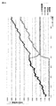
図26は、実際の測定データを実施形態1に基づいて、補正処理を実施した際の補正後の位相の補償量を示した図である。
このように上記実施形態では、補償回路部201からの位相補償量を補償量監視部202で監視しているので、スリップが発生した際、スリップによる位相補償量の変化をスリップ補正部で補正することが出来る。
さらに本実施形態では、補償量監視部202内に、補償変化量をKシンボル時間累積する累積部401が設けられている。そのため複数シンボル時間に跨ってスリップが発生した場合でも、スリップによる異常な補償量の変化を検出することが可能であり、その異常な補償量をスリップ補正部203で、補正することができる。
以上説明したように、本発明によれば、差動符号化を用いることなく、スリップによる位相のずれを補償することが可能であり、入力シンボルに対する位相補償量の期待値(図14のα−4)により補償された信号を出力することができる。
なお、上記実施形態では、スリップ発生箇所を特定するために、補償量の変化を監視している。しかし、補償量の変化の代わりに図10に示すフィルタ部102の出力信号(周波数オフセット量と称する場合もある。)を、使用しても良い。または、フィルタ部102の出力信号の変化を補償量の変化と併せて使用しても良い。
また、上記実施形態では、補償回路部内で、位相補償量を入力信号に反映し、そのデータを後段へ出力しているが、スリップ補正部203で、最終的にスリップキャンセルされた補償量を適用してもよい。
(第2の実施形態)
本発明の他の実施形態として、その基本的構成は上記の通りであるが、補償変化量閾値の生成についてさらに工夫している。その構成を図20に示す。図において、図8に示す補償変化量閾値設定部204を、補償変化量閾値決定部205に変更したことを除き、補償回路部201、補償量監視部202、スリップ補正部203は、図8に示す第1の実施形態と同様の構成である。補償変化量閾値決定部205は、スリップ発生を検出するのに使用する補償変化量閾値を決定する。
図21を参照すると、図20に示す補償変化量閾値決定部205の構成が示される。補償変化量閾値決定部205は、平均変化量計算部601、および閾値計算部602により構成される。
平均変化量計算部601は、遅延補償変化量の移動平均を計算し、その計算結果を閾値決定部602へ出力する。
閾値決定部602は、平均補償変化量に基づいて補償変化量閾値を計算する。本実施形態では、一例として、平均補償変化量と係数信号から、補償変化量閾値を計算し、補償量監視部202へ出力する。なお、図示していないが係数信号は、CPU等の制御部に接続される。
(動作)
図21における平均変化量計算部601に、遅延補償変化量とスリップ信号が、補償量監視部202から与えられる。すると、平均変化量計算部601は、スリップ信号の値が‘0’の場合のみ、Wシンボル時間の遅延補償変化量の移動平均を計算し、その計算結果を平均補償変化量Vとして、閾値決定部602へ出力する。スリップ信号の値が‘0’の場合のみ、移動平均の計算をおこなうため、この平均補償変化量には、スリップ発生時の補償量が含まれない。スリップ信号の値が‘0’の場合とはスリップが発生していない状態を意味するからである。
閾値決定部602に、平均補償変化量Vが、平均補償変化量計算部601から与えられる。すると、閾値決定部602は、一例として式(1)に示すように平均補償変化量にKを乗じ、さらに係数信号βを乗じた値を補償変化量閾値thとして、補償量監視部202へ出力する。Kは、図12に示す累積部401の累積シンボル時間であり、係数信号βは、移動平均からの乖離率を示す。この係数信号βは補償変化量閾値thの値を適切に調整するために設定されるものである。
補償変化量閾値th=平均補償変化量V × K × β ・・・(1)
なお、上記以外の補償回路部201、補償量監視部202、スリップ補正部203は、実施形態1と同様の動作を行う。
このように、本実施形態では、スリップの発生を検出するのに使用する補償変化量閾値を、遅延補償変化量とスリップ信号から生成している。そのため補償変化量が変化した場合でも、適切な補償変化量閾値を得ることができる。このため、補正誤りによる誤りを抑えるという効果が得られる。
(第3の実施形態)
本発明の他の実施形態として、その基本的構成は上記の通りであるが、補償変化量閾値の生成についてさらに工夫している。その構成を図22に示す。本図において、図20に示す実施形態2の構成に、同期パターン挿入部701、変調部702、同期部206を追加している以外、図20に示す第2の実施形態と同様の構成である。
同期パターン挿入部701、変調部702は、送信側に配置し、図示していないが、同期パターン挿入部の入力側には、SD−FECエンコード部、フレーマー部が配置される。
同期パターン挿入部701は、SD−FECエンコード部からの出力データに同期パターンを挿入し、変調部702へ出力する。
変調部702は、同期パターンより入力したデータを変調し、受信側へと送信する。
本実施形態では、変調方式としてQPSKを挙げ説明するが、特にこれに限定しない。また、変調部702と、補償回路部201間には、図示しないが、受信した信号の復調などを行う回路が配置される。
同期部206は、スリップ補正部203、補償量監視部202、補償変化量決定部205に接続され、補正シンボル信号より、同期パターンを検出し、補正シンボル信号の位相の正常性確認を行う。また、同期パターン検出後、同期外れが発生した場合、スリップ信号の状態により、補正シンボル信号の位相量を再度補正する。さらに、補償変化量閾値決定部205内で、補償変化量閾値を計算する際に使用する係数信号を更新する。なお、係数信号を更新する具体的な手順については後述する。
(動作)
次に、図23、図24、図25を使用し、図22に示す実施形態3の、同期パターン挿入部701、変調部702、および同期部206の動作を説明する。なお、その他の構成部の動作については、実施形態2と同様の動作となる。
図23は、送信側に配置される同期パターン挿入部701の入力信号と出力信号を示した図である。(イ)の同期パターン挿入部701の入力信号は、フレーマー部でyビット毎にフレーム化され、SD−FECエンコード部で計算されたパリティーを含む。図内UW(Unique Word)は、フレームのヘッダであり、DATAは、ユーザデータであり、Pは、SD−FECエンコード部で計算されたパリティー値が設定されている。なお、本実施形態では、一例としてyビットを32768ビット(4096バイト)として説明する。
(ロ)の同期パターン挿入部701の出力信号は、I,Qの2ビット幅で出力される。これは、変調部702での変調方式がQPSKであることに起因しているためである。本実施形態では、同期パターン挿入部で挿入するパターンを以下の条件に従い挿入する。
条件1:UWの先頭データである場合、同期パターンα−20として、Iに‘0’、Qに‘1‘を設定する。それ以外の場合、同期パターンα−21として、Iに‘1’、Qに‘0‘を設定する。
図22の同期パターン挿入部701において、図23(イ)の入力信号が与えられると、同期パターン挿入部701は、入力信号をUWからxビット毎に分離し、xビット毎に、条件1に対応した同期パターンを挿入し、変調部702へ出力する。なお、xは正の整数で、yの約数であり、本実施形態では、xビットを64ビットとして説明する。
変調部702に、図23の(ロ)に示す同期パターン挿入部出力信号が与えられると、変調部702は、入力されたI,Qを変調し、受信側へ送信する。
この様に送信側で条件1に従い同期パターンを挿入し変調されると、受信信号は32(xビット/2)シンボル時間毎に、図1に示すα−20、またはα−21に示す箇所に同期パターンが出現する。また受信信号は256(y/x/2)シンボル時間毎に、α−20に示す箇所に同期パターンが出現する。
次に、図24と図25を使用し、受信側に配置される同期部206の動作を説明する。両図において(イ)のI′、Q′は、スリップ補正部203から出力された補正シンボル信号を、複素数で表示した図である。両図における(ロ)の同期信号は、同期部206内の同期状態を示しており、α−18の箇所で同期外れが発生している。両図における(ハ)は、補償量監視部202から出力されたスリップ信号である。
両図における(ニ)は、同期部206から出力される再補正されたシンボル信号1′′、Q′′である。また、(ホ)の係数信号βは、同期部206から補償変化量閾値決定部205へ出力される信号であり、補償変化量閾値を計算するのに使用される。
なお、図24は、スリップ補正部203の補正により、補正誤りが生じた場合の図であり、α−17は補正誤りの箇所を示している。また、図25は、スリップ補正部203で補正しきれない場合の図であり、図内(イ)のα−21以降での何処かでスリップが発生している。
まず、図24を使用し、スリップ補正部203の補正により、補正誤りが生じた場合の、同期部206の動作について以下に説明する。
図22において、同期部206に、図24(イ)に示す補正シンボル信号が与えられると、同期部206は、補正シンボル信号(I′,Q′)から、同期パターン挿入部701で挿入された同期パターンの検出を行い、図内(ロ)の同期信号を生成する。
図24において、α−18の箇所で、同期外れが発生すると、同期部206は、同期外れ直前のスリップ信号の値が‘1’である箇所α−22より、補正シンボル信号の再補正を行う。なお補正量は、同期パターンとの差とすることができる。
さらに、スリップ信号生成の閾値をより上げることにより、スリップ信号生成の閾値が適切でないために発生する補正誤りを防ぐことができる。具体的には、スリップ信号生成の閾値の係数である係数信号βの値を、β(r−1)<β(r)になるように増加させ、補償変化量閾値決定部へ出力する。これは、現状の補償変化量閾値thが、低いことにより補正誤りが発生しているためであり、補償変化量閾値thを適切な値にするための処理である。rは任意のシンボル時間である。
次に、図25を使用し、スリップ補正部203でスリップが補正しきれない場合の、同期部206の動作について以下に説明する。
図22において、同期部206に、図25(イ)に示す補正シンボル信号が与えられると、同期部206は、補正シンボル信号(I′,Q′)から、同期パターン挿入部701で挿入された同期パターンの検出を行い、図内(ロ)の同期信号を生成する。
図25において、α−18の箇所で、同期外れが発生する。その時、同期部206は、図25(ハ)に示すスリップ信号が、‘0’である場合、図25のα−19に示す同期パターンの中間である(xビット/2=32ビット)の箇所から、補正シンボル信号の再補正を行う。
スリップ信号の値が‘0’である場合、スリップの発生箇所が不明であり、スリップの再補正箇所を決定する必要がある。このため前記処理では、スリップが、同期パターン間(xビット=64ビット)で、1回発生したと仮定し、スリップによる誤りを32ビット(xビット/2)以下に抑える。なお補正量は、同期パターンとの差とすることができる。
さらに、スリップ信号生成の閾値をより下げることにより、スリップ信号生成の閾値が適切でないために発生する補正誤りを防ぐことができる。具体的には、同期部206は、スリップ信号生成の閾値の係数である係数信号βの値を、β(u−1)>β(u)になるように減少させ、補償変化量閾値決定部へ出力する。これは、現状の補償変化量閾値thが、大きいことにより補正誤りが発生しているためであり、補償変化量閾値thを適切な値にするための処理である。uは任意のシンボル時間である。
このように、本実施形態では、送信側の同期バターン挿入部701で同期バターンを挿入し、同期部206で検出することで、スリップの発生を検出するのに使用する補償変化量閾値を制御している。具体的には、補償変化量閾値の係数信号βを生成している。そのため、スリップの誤検出を抑えることができるため、伝送特性を向上させる効果が得られる。
また、同期部206で、同期外れ(スリップ発生)を検出した場合、スリップ信号の状態に応じて、再補正を行うことができるため、前段部での誤補正による誤りを押さえることができるため、伝送特性を向上させる効果が得られる。
(効果)
第1の効果は、光通信システムの伝送特性を3dB向上できる。その理由は、差動符号化を用いることなく、スリップによるマッピングのズレを補正することが可能なことにある。
第2の効果は、光通信システムの伝送特性を向上できる。その理由は、差動符号化を用いることがないため、高誤り訂正利得が期待できるSD−FECのLLRの計算を複雑な処理を追加することなく実現できることにある。
第3の効果は、光通信システムの伝送特性を向上できる。その理由は、送信側で、信号に挿入された同期パターンを、受信側で検出することで、スリップによる影響を、同期パターン間内におさえることができるためである。つまり、同期パターン間隔より大きい誤りは発生しないことになる。
第4の効果は、光通信システムの伝送特性を向上できる。その理由は、送信側で、信号に挿入された同期パターンを、受信側で検出し、同期パターン間に発生した、スリップ数により、スリップ検出閾値である補償変化量閾値を適切な値へ変更することができる。それによって、スリップよる誤りを抑えることが可能なためである。
(第4の実施形態)
本発明の第4の実施形態を図27を参照して説明する。
本実施形態の位相変調信号復調器の位相偏差補償回路2701は、位相偏差補償回路により受信信号になされる位相補償量の変化から、受信信号のスリップの発生を検出し、スリップ発生以降の受信信号の位相補償量を補正することを特徴とする。
以上の構成により、本実施形態の位相変調信号復調器の位相偏差補償回路においては、下記の効果を有する。
即ち光位相偏差・光搬送波周波数偏差補償処理を実装する場合においても、伝送特性を低下させることなく、送信データを正しく復調可能なスリップ補償方法(光位相偏差・光搬送波周波数偏差補償方法)を提供できる。
(第5の実施形態)
本発明の第5の実施形態として、その基本構成は、第1の実施形態の通りであるが、補正量の生成についてさらに工夫している。その構成は、図8に示すスリップ補正部203をスリップ補正部207に変更したことを除き、図8に示す第1の実施形態と同様の構成である。スリップ補正部207は、スリップ補正部203内で計算される補正量に、「平均補償変化量」を適用することを除き、スリップ補正部203と同一のブロックである。
図28を参照すると、図に示すスリップ補正部207の構成が示される。平均補償変化量計算部601は、遅延補償変化量の移動平均を計算し、補正量計算部502へ出力する。
補正量計算部502は、補償量監視部202から出力される遅延補償変化量、スリップ信号、および平均補償変化量計算部601からの平均補償変化量から、補正量を計算し、出力する。補正量計算部502により算出された補正量は、複素数(位相補償量をφとするとexp(−iφ)で表される)と入力信号との積が出力信号として出力される。
(動作)
図28における補正量計算部502に、補償量監視部202から遅延補償変化量とスリップ信号と、平均補償変化量計算部601ら平均補償変化量が与えられる。すると、補正量計算部502は、スリップ信号の値が位相スリップの未発生を示す値‘0’の場合、遅延補償変化量と補正量の加算を行わず、1シンボル時間前の補正量を出力する。補正量計算部501は、スリップ信号の値が‘1’である場合、以下のように補正量B(t)と遅延補償変化量D(t)、平均補償変化量AVE(t)の和を、補正量として、出力する。tは任意のシンボル時間である。
B(t + 1)=B(t)+ D(t)+ AVE(t) ・・・(2)
図29は、本実施形態の補正量計算部502の出力信号を示した図であり、図29に示す(イ)遅延一次補償シンボル信号H(−1)~H(15)は、図8における補償量監視部202の出力信号である。図29における(ロ)補正シンボル信号C(3)~C(19)は、スリップ補正部207から出力される位相補正された補正シンボル信号である。なお、図におけるグラフα−10は、(イ)の一次補償シンボル信号に適用された補償量を示す。また、グラフα−15は、第1の実施形態における補正シンボル信号に適用された位相の補正量を、グラフα−17は、本実施形態における補正信号に適用された補正量を示す。図内のα−18~20で、上記式(2)で生成された補正値が適用されている。
なお、上記以外の補償回路部201、補償量監視部202は、補償変化量閾値設定部204は、第1の実施形態と同様の動作を、平均補償変化量計算部601は、第2の実施形態と同様の動作を行う。
このように、本実施形態では、第1の実施形態で、スリップ発生時の補償量をキャンセルする補正量を生成していたのに対し次の点が異なっている。即ち、キャンセルした補償量に平均補償変化量を加算するため、スリップ発生時に、増加(または減少)すべき変化量を加味した補正量を生成している。このため、スリップの発生による、位相のずれを抑えるという効果が得られる。
なお、ここまで説明した各実施形態では、専用の装置を想定したが、次のようなものでもよい。即ち例えば各種データ処理を行うパーソナルコンピュータ装置に、本例に相当する処理を行うボードやカードなどを装着し、各処理を、コンピュータ装置側で実行させる。このようにして、その処理を実行するソフトウェアをパーソナルコンピュータ装置に実装させて実行する構成としても良い。
そのパーソナルコンピュータ装置などのデータ処理装置に実装されるプログラムについては、光ディスク,メモリカードなどの各種記録(記憶)媒体を介して配付しても良い。或いはインターネットなどの通信手段を介して配付しても良い。
また、以上の実施形態は各々他の実施形態と組み合わせることができる。
以上、実施形態を参照して本願発明を説明したが、本願発明は上記実施形態に限定されるものではない。本願発明の構成や詳細には、本願発明のスコープ内で当業者が理解し得る様々な変更をすることができる。
以上に述べた実施形態の一部又は全部は、以下の付記のようにも記載されうるが、以下には限られない。
(付記1)
位相偏差補償手段により受信信号になされる位相補償量の変化から、受信信号のスリップの発生を検出し、スリップ発生以降の受信信号の位相補償量を補正することを特徴とする位相変調信号復調器の位相偏差補償回路。
(付記2)
入力信号に対し位相偏差の補償を行う位相補償手段と、
前記位相補償手段における位相補償量の変化を監視しスリップ発生の検出を行うスリップ検出手段と、
前記スリップ検出手段で検出したスリップによって生じた位相変化分を補正するスリップ補正手段と、
を備えたことを特徴とする位相変調信号復調器の位相偏差補償回路。
(付記3)
前記スリップの検出は、前記位相補償手段における位相補償の変化量が所定の閾値を超えることにより検出する、
ことを特徴とする付記2記載の位相変調信号復調器の位相偏差補償回路。
(付記4)
前記閾値が前記位相補償の変化量の移動平均に基づいて決められる
ことを特徴とする付記3記載の位相変調信号復調器の位相偏差補償回路。
(付記5)
受信信号に挿入された同期パターンを検出し、前記位相補償量の再補正を行う同期手段を有する、
ことを特徴とする付記1乃至付記4いずれかに記載の位相変調信号復調器の位相偏差補償回路。
(付記6)
前記同期パターンは、フレームの先頭と、その他の位置とで異なるパターンをもつことを特徴とする付記5記載の位相変調信号復調器の位相偏差補償回路。
(付記7)
前記位相偏差補償回路は搬送波周波数偏差の補償も含む
ことを特徴とする付記1乃至付記6のいずれかに記載の位相変調信号復調器の位相偏差補償回路。
(付記8)
付記1乃至7のいずれかに記載の位相変調信号復調器の位相偏差補償回路を備えることを特徴とする光伝送受信装置。
(付記9)
付記1乃至8のいずれかに記載の光伝送受信装置
を備えることを特徴とする光伝送通信システム。
(付記10)
受信信号の位相補償量の変化から、受信信号のスリップの発生を検出し、スリップ発生後の受信信号の位相補償量を補正することを特徴とする位相偏差補償方法。
(付記11)
入力信号に対し位相偏差の補償を行い、
位相補償量の変化を監視しスリップ発生の検出を行い、
スリップによって生じた位相変化分を補正する
ことを特徴とする位相偏差補償方法。
(付記12)
前記スリップの検出は、位相補償の変化量が所定の閾値を超えることにより検出する、
ことを特徴とする付記11記載の位相偏差補償方法。
(付記13)
前記閾値が前記位相補償の変化量の移動平均に基づいて定められる
ことを特徴とする付記12記載の位相偏差補償方法。
(付記14)
受信信号に挿入された同期パターンを検出し、前記位相補償量の再補正を行う、
ことを特徴とする付記10乃至付記13いずれかに記載の位相偏差補償方法。
(付記15)
前記同期パターンは、フレームの先頭と、その他の位置とで異なるパターンをもつことを特徴とする付記14記載の位相偏差補償方法。
(付記16)
入力信号に対し位相偏差の補償を行う位相補償処理と、
前記位相補償処理における位相補償量の変化を監視しスリップ発生の検出を行うスリップ検出処理と、
前記スリップ検出処理で検出したスリップによって生じた位相変化分を補正するスリップ補正処理と、
をコンピュータに実施させることを特徴とする位相偏差補償プログラム。
この出願は、2011年3月25日に出願された日本出願特願2011−067699を基礎とする優先権を主張し、その開示の全てをここに取り込む。
102 フィルタ部
103 位相補償量算出部
104 差動符号復調部
201 補償回路部(光位相偏差・光搬送波周波数偏差補償回路)
202 補償量監視部
203 スリップ補正部
204 補償変化量閾値設定部
205 補償変化量閾値決定部
206 同期部
207 スリップ補正部
301 シンボル時間遅延部
302 補償変化量検出部
303 補償変化量比較部
304 シンボルタイミング調整部
401 累積部
402 比較部
403 遅延部
501 補正量計算部
502 補正量計算部
601 平均補償変化量計算部
602 閾値計算部
701 同期パターン挿入部
702 変調部
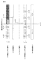
Claims (16)
- 位相偏差補償手段により受信信号になされる位相補償量の変化から、受信信号のスリップの発生を検出し、スリップ発生以降の受信信号の位相補償量を補正することを特徴とする位相変調信号復調器の位相偏差補償回路。
- 入力信号に対し位相偏差の補償を行う位相補償手段と、
前記位相補償手段における位相補償量の変化を監視しスリップ発生の検出を行うスリップ検出手段と、
前記スリップ検出手段で検出したスリップによって生じた位相変化分を補正するスリップ補正手段と、
を備えたことを特徴とする位相変調信号復調器の位相偏差補償回路。 - 前記スリップの検出は、前記位相補償手段における位相補償の変化量が所定の閾値を超えることにより検出する、
ことを特徴とする請求項2記載の位相変調信号復調器の位相偏差補償回路。 - 前記閾値が前記位相補償の変化量の移動平均に基づいて決められる
ことを特徴とする請求項3記載の位相変調信号復調器の位相偏差補償回路。 - 受信信号に挿入された同期パターンを検出し、前記位相補償量の再補正を行う同期手段を有する、
ことを特徴とする請求項1乃至請求項4いずれかに記載の位相変調信号復調器の位相偏差補償回路。 - 前記同期パターンは、フレームの先頭と、その他の位置とで異なるパターンをもつことを特徴とする請求項5記載の位相変調信号復調器の位相偏差補償回路。
- 前記位相偏差補償回路は搬送波周波数偏差の補償も含む
ことを特徴とする請求項1乃至請求項6のいずれかに記載の位相変調信号復調器の位相偏差補償回路。 - 請求項1乃至7のいずれかに記載の位相変調信号復調器の位相偏差補償回路を備えることを特徴とする光伝送受信装置。
- 請求項1乃至8のいずれかに記載の光伝送受信装置
を備えることを特徴とする光伝送通信システム。 - 受信信号の位相補償量の変化から、受信信号のスリップの発生を検出し、スリップ発生後の受信信号の位相補償量を補正することを特徴とする位相偏差補償方法。
- 入力信号に対し位相偏差の補償を行い、
位相補償量の変化を監視しスリップ発生の検出を行い、
スリップによって生じた位相変化分を補正する
ことを特徴とする位相偏差補償方法。 - 前記スリップの検出は、位相補償の変化量が所定の閾値を超えることにより検出する、
ことを特徴とする請求項11記載の位相偏差補償方法。 - 前記閾値が前記位相補償の変化量の移動平均に基づいて定められる
ことを特徴とする請求項12記載の位相偏差補償方法。 - 受信信号に挿入された同期パターンを検出し、前記位相補償量の再補正を行う、
ことを特徴とする請求項10乃至請求項13いずれかに記載の位相偏差補償方法。 - 前記同期パターンは、フレームの先頭と、その他の位置とで異なるパターンをもつことを特徴とする請求項14記載の位相偏差補償方法。
- 入力信号に対し位相偏差の補償を行う位相補償処理と、
前記位相補償処理における位相補償量の変化を監視しスリップ発生の検出を行うスリップ検出処理と、
前記スリップ検出処理で検出したスリップによって生じた位相変化分を補正するスリップ補正処理と、
をコンピュータに実施させることを特徴とする位相偏差補償プログラム。
Priority Applications (2)
| Application Number | Priority Date | Filing Date | Title |
|---|---|---|---|
| US14/005,238 US9184905B2 (en) | 2011-03-25 | 2011-11-15 | Phase compensation receiver |
| JP2012530438A JP5234228B2 (ja) | 2011-03-25 | 2011-11-15 | 位相補償受信器 |
Applications Claiming Priority (2)
| Application Number | Priority Date | Filing Date | Title |
|---|---|---|---|
| JP2011067699 | 2011-03-25 | ||
| JP2011-067699 | 2011-03-25 |
Publications (1)
| Publication Number | Publication Date |
|---|---|
| WO2012132103A1 true WO2012132103A1 (ja) | 2012-10-04 |
Family
ID=46929902
Family Applications (1)
| Application Number | Title | Priority Date | Filing Date |
|---|---|---|---|
| PCT/JP2011/076741 WO2012132103A1 (ja) | 2011-03-25 | 2011-11-15 | 位相補償受信器 |
Country Status (3)
| Country | Link |
|---|---|
| US (1) | US9184905B2 (ja) |
| JP (1) | JP5234228B2 (ja) |
| WO (1) | WO2012132103A1 (ja) |
Cited By (10)
| Publication number | Priority date | Publication date | Assignee | Title |
|---|---|---|---|---|
| WO2013136716A1 (ja) * | 2012-03-14 | 2013-09-19 | 日本電気株式会社 | 光位相偏差・光搬送波周波数偏差補償装置および光位相偏差・光搬送波周波数偏差補償方法 |
| WO2014115840A1 (ja) * | 2013-01-25 | 2014-07-31 | 日本電信電話株式会社 | 光受信装置および位相サイクルスリップ低減方法 |
| WO2015052894A1 (ja) * | 2013-10-07 | 2015-04-16 | 日本電気株式会社 | 搬送波周波数偏差推定装置および搬送波周波数偏差推定方法 |
| JP2015204572A (ja) * | 2014-04-15 | 2015-11-16 | 富士通株式会社 | 通信システム、受信装置および半導体装置 |
| JP2015204573A (ja) * | 2014-04-15 | 2015-11-16 | 富士通株式会社 | 通信システム、受信装置および半導体装置 |
| JP2016505806A (ja) * | 2012-10-24 | 2016-02-25 | フェイスブック,インク. | 制御された帯域幅の複数のスケールを使用した無線装置間における距離の検知 |
| JPWO2015025468A1 (ja) * | 2013-08-21 | 2017-03-02 | 日本電気株式会社 | 周波数偏差補償方式、周波数偏差補償方法及びプログラム |
| WO2018177423A1 (zh) * | 2017-03-30 | 2018-10-04 | 深圳市中兴微电子技术有限公司 | 相位跳变纠正的方法及装置 |
| US10439732B2 (en) | 2016-09-09 | 2019-10-08 | Fujitsu Limited | Receiving device and phase-error compensation method |
| WO2020039505A1 (ja) * | 2018-08-21 | 2020-02-27 | 三菱電機株式会社 | 位相推定装置 |
Families Citing this family (1)
| Publication number | Priority date | Publication date | Assignee | Title |
|---|---|---|---|---|
| US8886058B2 (en) * | 2012-06-04 | 2014-11-11 | Cisco Technology, Inc. | Cycle slip reduction in coherent optical communications |
Citations (7)
| Publication number | Priority date | Publication date | Assignee | Title |
|---|---|---|---|---|
| JPS55110458A (en) * | 1979-02-19 | 1980-08-25 | Kokusai Denshin Denwa Co Ltd <Kdd> | Phase slip detector |
| JPH0211047A (ja) * | 1988-06-29 | 1990-01-16 | Matsushita Electric Ind Co Ltd | 搬送波再生回路 |
| JPH03289844A (ja) * | 1990-04-06 | 1991-12-19 | Nec Corp | データ復調装置 |
| JPH05103030A (ja) * | 1991-10-07 | 1993-04-23 | Nippon Telegr & Teleph Corp <Ntt> | 位相検波回路 |
| JPH11205399A (ja) * | 1998-01-14 | 1999-07-30 | Matsushita Electric Ind Co Ltd | Gmsk符号データ再生装置 |
| JP2002111766A (ja) * | 2000-10-03 | 2002-04-12 | Nec Corp | 復調装置 |
| JP2009135844A (ja) * | 2007-11-30 | 2009-06-18 | Icom Inc | 周波数制御装置、周波数制御方法、及び、プログラム |
Family Cites Families (5)
| Publication number | Priority date | Publication date | Assignee | Title |
|---|---|---|---|---|
| US4630286A (en) * | 1984-10-10 | 1986-12-16 | Paradyne Corporation | Device for synchronization of multiple telephone circuits |
| JP3453006B2 (ja) | 1995-07-07 | 2003-10-06 | パイオニア株式会社 | 位相同期回路及びディジタル信号再生装置 |
| JP3491480B2 (ja) | 1997-02-13 | 2004-01-26 | 三菱電機株式会社 | タイミング再生回路及びこれを用いた復調器 |
| US8139685B2 (en) * | 2005-05-10 | 2012-03-20 | Qualcomm Incorporated | Systems, methods, and apparatus for frequency control |
| JP2008226363A (ja) | 2007-03-13 | 2008-09-25 | Sony Corp | 記録媒体の再生装置及び再生方法 |
-
2011
- 2011-11-15 WO PCT/JP2011/076741 patent/WO2012132103A1/ja active Application Filing
- 2011-11-15 JP JP2012530438A patent/JP5234228B2/ja active Active
- 2011-11-15 US US14/005,238 patent/US9184905B2/en active Active
Patent Citations (7)
| Publication number | Priority date | Publication date | Assignee | Title |
|---|---|---|---|---|
| JPS55110458A (en) * | 1979-02-19 | 1980-08-25 | Kokusai Denshin Denwa Co Ltd <Kdd> | Phase slip detector |
| JPH0211047A (ja) * | 1988-06-29 | 1990-01-16 | Matsushita Electric Ind Co Ltd | 搬送波再生回路 |
| JPH03289844A (ja) * | 1990-04-06 | 1991-12-19 | Nec Corp | データ復調装置 |
| JPH05103030A (ja) * | 1991-10-07 | 1993-04-23 | Nippon Telegr & Teleph Corp <Ntt> | 位相検波回路 |
| JPH11205399A (ja) * | 1998-01-14 | 1999-07-30 | Matsushita Electric Ind Co Ltd | Gmsk符号データ再生装置 |
| JP2002111766A (ja) * | 2000-10-03 | 2002-04-12 | Nec Corp | 復調装置 |
| JP2009135844A (ja) * | 2007-11-30 | 2009-06-18 | Icom Inc | 周波数制御装置、周波数制御方法、及び、プログラム |
Cited By (17)
| Publication number | Priority date | Publication date | Assignee | Title |
|---|---|---|---|---|
| WO2013136716A1 (ja) * | 2012-03-14 | 2013-09-19 | 日本電気株式会社 | 光位相偏差・光搬送波周波数偏差補償装置および光位相偏差・光搬送波周波数偏差補償方法 |
| JP2016505806A (ja) * | 2012-10-24 | 2016-02-25 | フェイスブック,インク. | 制御された帯域幅の複数のスケールを使用した無線装置間における距離の検知 |
| WO2014115840A1 (ja) * | 2013-01-25 | 2014-07-31 | 日本電信電話株式会社 | 光受信装置および位相サイクルスリップ低減方法 |
| CN104919729A (zh) * | 2013-01-25 | 2015-09-16 | 日本电信电话株式会社 | 光接收装置和相位周跳减少方法 |
| CN104919729B (zh) * | 2013-01-25 | 2017-06-20 | 日本电信电话株式会社 | 光接收装置和相位周跳减少方法 |
| JP5886984B2 (ja) * | 2013-01-25 | 2016-03-16 | 日本電信電話株式会社 | 光受信装置および位相サイクルスリップ低減方法 |
| US9667350B2 (en) | 2013-01-25 | 2017-05-30 | Nippon Telegraph And Telephone Corporation | Optical receiving device and phase cycle reduction method |
| JPWO2015025468A1 (ja) * | 2013-08-21 | 2017-03-02 | 日本電気株式会社 | 周波数偏差補償方式、周波数偏差補償方法及びプログラム |
| WO2015052894A1 (ja) * | 2013-10-07 | 2015-04-16 | 日本電気株式会社 | 搬送波周波数偏差推定装置および搬送波周波数偏差推定方法 |
| JPWO2015052894A1 (ja) * | 2013-10-07 | 2017-03-09 | 日本電気株式会社 | 搬送波周波数偏差推定装置および搬送波周波数偏差推定方法 |
| JP2015204572A (ja) * | 2014-04-15 | 2015-11-16 | 富士通株式会社 | 通信システム、受信装置および半導体装置 |
| US9467318B2 (en) | 2014-04-15 | 2016-10-11 | Fujitsu Limited | Communication system, receiving device, and semiconductor device |
| US9438461B2 (en) | 2014-04-15 | 2016-09-06 | Fujitsu Limited | Communication system, receiving device, and semiconductor device |
| JP2015204573A (ja) * | 2014-04-15 | 2015-11-16 | 富士通株式会社 | 通信システム、受信装置および半導体装置 |
| US10439732B2 (en) | 2016-09-09 | 2019-10-08 | Fujitsu Limited | Receiving device and phase-error compensation method |
| WO2018177423A1 (zh) * | 2017-03-30 | 2018-10-04 | 深圳市中兴微电子技术有限公司 | 相位跳变纠正的方法及装置 |
| WO2020039505A1 (ja) * | 2018-08-21 | 2020-02-27 | 三菱電機株式会社 | 位相推定装置 |
Also Published As
| Publication number | Publication date |
|---|---|
| US20140003555A1 (en) | 2014-01-02 |
| JPWO2012132103A1 (ja) | 2014-07-24 |
| US9184905B2 (en) | 2015-11-10 |
| JP5234228B2 (ja) | 2013-07-10 |
Similar Documents
| Publication | Publication Date | Title |
|---|---|---|
| JP5234228B2 (ja) | 位相補償受信器 | |
| US9667350B2 (en) | Optical receiving device and phase cycle reduction method | |
| US10608743B2 (en) | Transmission characteristic compensation apparatus, transmission characteristic compensation method, and communication apparatus | |
| US10530493B2 (en) | Timing recovery for optical coherent receivers in the presence of polarization mode dispersion | |
| JP5482273B2 (ja) | 光受信器 | |
| CN104969524A (zh) | 光传输系统、相位补偿方法以及光接收装置 | |
| JP5672973B2 (ja) | フィードバックループを用いた周波数オフセット評価 | |
| JP5704077B2 (ja) | 位相偏差・搬送波周波数偏差補償装置および位相偏差・搬送波周波数偏差補償方法 | |
| EP2567461B1 (en) | Method and apparatus for detecting a parity error in a sequence of dqpsk symbols of a digital transmission system | |
| Zhang et al. | Pilot-assisted decision-aided maximum-likelihood phase estimation in coherent optical phase-modulated systems with nonlinear phase noise | |
| KR20120016294A (ko) | 위성 시스템의 개선된 동기 검출 및 주파수 복구 | |
| US20120148265A1 (en) | Coherent optical receiving device capable of digital equalization of optical input, digital equalization method for optical input and coherent optical transmitting/receiving device | |
| JP6191416B2 (ja) | 周波数オフセット推定回路および周波数オフセット推定方法 | |
| US20190280778A1 (en) | Pilot-Aided Digital Signal Processing for Reception of Coherent Optical Communication | |
| US9806823B2 (en) | Cycle slip compensation in a coherent receiver | |
| WO2016056395A1 (ja) | 受信装置、受信方法、およびプログラム | |
| JP7009890B2 (ja) | バイアスドリフト補償装置、受信信号復元装置及び受信機 | |
| US20110033191A1 (en) | Method and device for phase recovery and communication system comprising such device | |
| WO2019235568A1 (ja) | フレーム同期装置、光通信装置およびフレーム同期方法 | |
| WO2014187742A1 (en) | Apparatus, method and computer program for recovering a phase of a received signal | |
| JP2019213218A (ja) | フレーム同期装置、光通信装置およびフレーム同期方法 | |
| de Arruda Mello et al. | Carrier Recovery | |
| JP6156603B1 (ja) | 復調装置 | |
| JP2024025582A (ja) | 位相補償装置、光受信器および位相補償方法 | |
| BR102015013039A2 (pt) | método de estimação de desvios de frequência e/ou fase em sistemas de comunicação digital coerente |
Legal Events
| Date | Code | Title | Description |
|---|---|---|---|
| ENP | Entry into the national phase |
Ref document number: 2012530438 Country of ref document: JP Kind code of ref document: A |
|
| 121 | Ep: the epo has been informed by wipo that ep was designated in this application |
Ref document number: 11862616 Country of ref document: EP Kind code of ref document: A1 |
|
| WWE | Wipo information: entry into national phase |
Ref document number: 14005238 Country of ref document: US |
|
| NENP | Non-entry into the national phase |
Ref country code: DE |
|
| 122 | Ep: pct application non-entry in european phase |
Ref document number: 11862616 Country of ref document: EP Kind code of ref document: A1 |