WO2012131826A1 - 光電変換装置 - Google Patents
光電変換装置 Download PDFInfo
- Publication number
- WO2012131826A1 WO2012131826A1 PCT/JP2011/006887 JP2011006887W WO2012131826A1 WO 2012131826 A1 WO2012131826 A1 WO 2012131826A1 JP 2011006887 W JP2011006887 W JP 2011006887W WO 2012131826 A1 WO2012131826 A1 WO 2012131826A1
- Authority
- WO
- WIPO (PCT)
- Prior art keywords
- semiconductor layer
- silicon
- layer
- amorphous semiconductor
- particle
- Prior art date
- Legal status (The legal status is an assumption and is not a legal conclusion. Google has not performed a legal analysis and makes no representation as to the accuracy of the status listed.)
- Ceased
Links
Images




Classifications
-
- B—PERFORMING OPERATIONS; TRANSPORTING
- B82—NANOTECHNOLOGY
- B82Y—SPECIFIC USES OR APPLICATIONS OF NANOSTRUCTURES; MEASUREMENT OR ANALYSIS OF NANOSTRUCTURES; MANUFACTURE OR TREATMENT OF NANOSTRUCTURES
- B82Y20/00—Nanooptics, e.g. quantum optics or photonic crystals
-
- H—ELECTRICITY
- H10—SEMICONDUCTOR DEVICES; ELECTRIC SOLID-STATE DEVICES NOT OTHERWISE PROVIDED FOR
- H10F—INORGANIC SEMICONDUCTOR DEVICES SENSITIVE TO INFRARED RADIATION, LIGHT, ELECTROMAGNETIC RADIATION OF SHORTER WAVELENGTH OR CORPUSCULAR RADIATION
- H10F10/00—Individual photovoltaic cells, e.g. solar cells
- H10F10/10—Individual photovoltaic cells, e.g. solar cells having potential barriers
- H10F10/16—Photovoltaic cells having only PN heterojunction potential barriers
- H10F10/164—Photovoltaic cells having only PN heterojunction potential barriers comprising heterojunctions with Group IV materials, e.g. ITO/Si or GaAs/SiGe photovoltaic cells
- H10F10/165—Photovoltaic cells having only PN heterojunction potential barriers comprising heterojunctions with Group IV materials, e.g. ITO/Si or GaAs/SiGe photovoltaic cells the heterojunctions being Group IV-IV heterojunctions, e.g. Si/Ge, SiGe/Si or Si/SiC photovoltaic cells
- H10F10/166—Photovoltaic cells having only PN heterojunction potential barriers comprising heterojunctions with Group IV materials, e.g. ITO/Si or GaAs/SiGe photovoltaic cells the heterojunctions being Group IV-IV heterojunctions, e.g. Si/Ge, SiGe/Si or Si/SiC photovoltaic cells the Group IV-IV heterojunctions being heterojunctions of crystalline and amorphous materials, e.g. silicon heterojunction [SHJ] photovoltaic cells
-
- H—ELECTRICITY
- H10—SEMICONDUCTOR DEVICES; ELECTRIC SOLID-STATE DEVICES NOT OTHERWISE PROVIDED FOR
- H10F—INORGANIC SEMICONDUCTOR DEVICES SENSITIVE TO INFRARED RADIATION, LIGHT, ELECTROMAGNETIC RADIATION OF SHORTER WAVELENGTH OR CORPUSCULAR RADIATION
- H10F77/00—Constructional details of devices covered by this subclass
- H10F77/10—Semiconductor bodies
- H10F77/14—Shape of semiconductor bodies; Shapes, relative sizes or dispositions of semiconductor regions within semiconductor bodies
- H10F77/143—Shape of semiconductor bodies; Shapes, relative sizes or dispositions of semiconductor regions within semiconductor bodies comprising quantum structures
- H10F77/1433—Quantum dots
-
- Y—GENERAL TAGGING OF NEW TECHNOLOGICAL DEVELOPMENTS; GENERAL TAGGING OF CROSS-SECTIONAL TECHNOLOGIES SPANNING OVER SEVERAL SECTIONS OF THE IPC; TECHNICAL SUBJECTS COVERED BY FORMER USPC CROSS-REFERENCE ART COLLECTIONS [XRACs] AND DIGESTS
- Y02—TECHNOLOGIES OR APPLICATIONS FOR MITIGATION OR ADAPTATION AGAINST CLIMATE CHANGE
- Y02E—REDUCTION OF GREENHOUSE GAS [GHG] EMISSIONS, RELATED TO ENERGY GENERATION, TRANSMISSION OR DISTRIBUTION
- Y02E10/00—Energy generation through renewable energy sources
- Y02E10/50—Photovoltaic [PV] energy
- Y02E10/547—Monocrystalline silicon PV cells
Definitions
- the present invention relates to a photoelectric conversion device suitable for a solar cell.
- an i-type amorphous silicon layer and a p-type amorphous silicon layer are stacked on the front side of n-type crystalline silicon, and an i-type amorphous silicon layer is formed on the back side.
- a structure in which an n-type amorphous silicon layer is stacked is known (for example, see Patent Document 1).
- the present invention has been made in view of such circumstances, and an object thereof is to provide a technique for improving the conversion efficiency in the photoelectric conversion device.
- a photoelectric conversion device includes a one-conductivity type crystalline semiconductor layer, an intrinsic amorphous semiconductor layer formed on one surface of the crystalline semiconductor layer, and an intrinsic A fine particle-containing layer containing semiconductor fine particles formed on the amorphous semiconductor layer, and formed on the fine particle-containing layer and having an opposite conductivity type to the crystalline semiconductor layer or a crystalline semiconductor And an amorphous semiconductor layer of the same conductivity type as the layer.
- the semiconductor fine particles include particles having a particle size in the range of 4 to 7 nm.
- the conversion efficiency in the photoelectric conversion device can be improved.
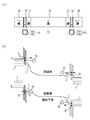
- FIG. 2A schematically shows a layer structure of the photoelectric conversion device according to this embodiment
- FIG. 2B schematically shows a band diagram of the photoelectric conversion device according to this embodiment.
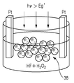
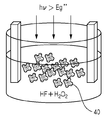
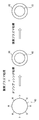
- FIG. It is a schematic diagram for demonstrating the manufacturing method of the silicon nanoparticle which concerns on this Embodiment. It is a schematic diagram for demonstrating the manufacturing method of the silicon nanoparticle which concerns on this Embodiment. It is a schematic diagram for demonstrating the manufacturing method of the silicon nanoparticle which concerns on this Embodiment. It is a schematic diagram for demonstrating the manufacturing method of the silicon nanoparticle which concerns on this Embodiment. It is a schematic diagram for demonstrating the manufacturing method of the silicon nanoparticle which concerns on this Embodiment.
- FIG. 1 is a cross-sectional view of the photoelectric conversion device according to this embodiment.
- the scales and shapes of each layer and each part shown in the following drawings are set for convenience of explanation, and are not limitedly interpreted unless otherwise specified.
- the photoelectric conversion device 10 is formed on one conductivity type crystal semiconductor layer 12 and one surface (upper surface shown in FIG. 1) of the crystal semiconductor layer 12.
- Intrinsic amorphous semiconductor layer 14 formed on intrinsic amorphous semiconductor layer 14, formed on fine particle-containing layer 16 containing semiconductor fine particles, and fine particle-containing layer 16, and formed on crystalline semiconductor layer 12
- the photoelectric conversion device 10 includes an intrinsic amorphous semiconductor layer 24 formed on the other surface (the lower surface shown in FIG. 1) of the crystalline semiconductor layer 12, and an intrinsic amorphous semiconductor.
- the crystalline semiconductor layer 12 is n-type single crystal silicon.
- the n-type single crystal silicon suitable for this embodiment has a resistivity of about 1 ⁇ ⁇ cm and a thickness of 200 to 300 ⁇ m.
- the intrinsic amorphous semiconductor layer 14 is an i-type amorphous silicon (a-Si) semiconductor and has a thickness of about 10 nm on the upper surface of the crystalline semiconductor layer 12 using a known RF plasma CVD (13.56 MHz) method. It is formed into a film.
- the fine particle-containing layer 16 is a semiconductor layer containing semiconductor fine particles 16c, as shown in FIG.
- the semiconductor fine particles 16c are preferably composed only of particles having a particle size (particle diameter) in the range of 4 to 7 nm.
- the present invention is not limited to this, and it may be composed of particles having different particle diameters, for example, a particle group having a particle size distribution peak in the range of 4 to 7 nm.
- the semiconductor fine particles 16c are composed of silicon nanoparticles 16a and an insulating film 16b covering the periphery (surface).
- the silicon nanoparticles 16a are made of single-crystal silicon or polycrystalline silicon, which is crystalline silicon, in a nano-level powder form (powder form), and the size (particle diameter) of the particles is in the range of 2 to 3 nm.
- the present invention is not limited to this, and may be composed of particles having different particle diameters. For example, a particle group having a particle size distribution peak in the range of 2 to 3 nm. Also good.
- the insulating film 16b is a silicon oxide film (SiO), a silicon oxynitride film (SiON), a silicon nitride film (SiN), or the like.
- the insulating film 16b has a thickness of about 1 to 2 nm.
- the fine particle-containing layer 16 is formed on the intrinsic amorphous semiconductor layer 14 so as to have a thickness of about 10 to 30 nm, for example, by an aerosol deposition method described later.
- the first amorphous semiconductor layer 18 is a p-type amorphous silicon (a-Si) semiconductor, and is formed on the fine particle-containing layer 16 so as to have a thickness of about 10 nm using a known RF plasma CVD method.
- the transparent conductive film 20 is an ITO film in which several percent of tin oxide (SnO 2 ) is added to indium oxide (In 2 O 3 ).
- the transparent conductive film 20 is formed to a thickness of about 100 nm on the first amorphous semiconductor layer 18 using a known sputtering method.
- the photoelectric conversion device 10 has a light receiving surface on the side where the transparent conductive film 20 is provided.
- the comb-shaped electrode 22 has a conductive filler made of silver (Ag) and a thermosetting resin.
- a predetermined pattern including a finger portion and a bus bar portion is formed in a predetermined region on the surface of the transparent conductive film 20 by printing.
- the intrinsic amorphous semiconductor layer 24 is an i-type amorphous silicon (a-Si) semiconductor, and is formed on the lower surface of the crystalline semiconductor layer 12 to have a thickness of about 10 nm using a known RF plasma CVD method. It is a membrane.
- a-Si i-type amorphous silicon
- the fine particle-containing layer 26 is a semiconductor layer containing semiconductor fine particles 26c, as shown in FIG.
- the semiconductor fine particles 26c are preferably composed only of particles having a particle size (particle diameter) in the range of 4 to 7 nm.
- the present invention is not limited to this, and it may be composed of particles having different particle diameters, for example, a particle group having a particle size distribution peak in the range of 4 to 7 nm.
- the semiconductor fine particles 26c are composed of silicon nanoparticles 26a and an insulating film 26b covering the periphery (surface).
- the silicon nanoparticles 26a are produced by producing single-crystal silicon or polycrystalline silicon, which is crystalline silicon, into a nano-level powder (powder), and the size (particle size) of the particles is in the range of 2 to 3 nm.
- the present invention is not limited to this, and may be composed of particles having different particle diameters. For example, a particle group having a particle size distribution peak in the range of 2 to 3 nm. Also good.
- the insulating film 16b is a silicon oxide film (SiO), a silicon oxynitride film (SiON), a silicon nitride film (SiN), or the like.
- the insulating film 16b has a thickness of about 1 to 2 nm.
- the fine particle-containing layer 26 is formed to have a thickness of about 10 to 30 nm under the intrinsic amorphous semiconductor layer 24 by, for example, an aerosol deposition method described later.
- the second amorphous semiconductor layer 28 is an n-type amorphous silicon (a-Si) semiconductor, and is formed to a thickness of about 10 nm under the fine particle-containing layer 26 using a known RF plasma CVD method.
- the transparent conductive film 30 is an ITO film in which several percent of tin oxide (SnO 2 ) is added to indium oxide (In 2 O 3 ).
- the transparent conductive film 30 is formed to a thickness of about 100 nm under the second amorphous semiconductor layer 28 using a known sputtering method.
- the comb electrode 32 has a conductive filler made of silver (Ag) and a thermosetting resin.
- a predetermined pattern including finger portions and bus bar portions is formed in a predetermined region on the surface of the transparent conductive film 30 by printing.
- FIG. 2A schematically shows a layer structure of the photoelectric conversion device according to this embodiment
- FIG. 2B schematically shows a band diagram of the photoelectric conversion device according to this embodiment.
- the p-type a-Si layer, the i-type a-Si layer, and the n-type a-Si layer include many localized levels L, so that a leakage current flows in the state as it is. It becomes easy. Therefore, in the photoelectric conversion device 10 according to the present embodiment, the fine particle-containing layer 16 including the silicon nanoparticles 16a covered with the insulating film 16b between the i-type a-Si layer and the p-type a-Si layer. Is sandwiched. In the photoelectric conversion device 10, the fine particle-containing layer 26 including the silicon nanoparticles 26a covered with the insulating film 26b is sandwiched between the i-type a-Si layer and the n-type a-Si layer.
- Ec represents the energy at the lower end of the conductor
- Ev represents the energy at the upper end of the valence band.
- the band gap due to the silicon nanoparticles 16a is narrow, and the band gap due to the insulating film 16b is wide.
- a plurality of minibands B are formed at a position higher than the bottom of the well by the silicon nanoparticles 16a.
- the resonant tunnel diode is formed by the energy level in the miniband formed by the silicon nanoparticles 16a constituting the semiconductor fine particles 16c.
- the band gap of the miniband B is about 2 eV, which is larger than about 1.7 eV of amorphous silicon. Therefore, carriers are prevented from leaking to the p (n) type amorphous silicon layer through the low localized level in the amorphous silicon.
- the open-circuit voltage Voc which is one of the indexes that determine the characteristics of the photoelectric conversion device (solar cell)
- the conversion efficiency ⁇ of the solar cell is expressed by Expression (1).
- Voc Open circuit voltage
- Isc Short circuit current density
- FF Curve factor
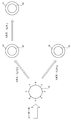
- FIG. 3 to 6 are schematic views for explaining the method for producing silicon nanoparticles according to the present embodiment.
- HF hydrofluoric acid
- H 2 O 2 hydrogen peroxide solution
- silicon powder containing silicon as a main component is prepared.
- the silicon powder may be concentrated and separated from the silicon waste water treatment apparatus. Such silicon powder is also suitable from the viewpoint of recycling the silicon material.
- the silicon powder 38 is immersed in a mixed solution of HF + H 2 O 2 (+ methanol) together with a platinum (Pt) electrode.
- the particle size of the silicon powder 38 at this time is several ⁇ m to several mm.
- the wavelength of the irradiation light is set so that h ⁇ > Eg ′.
- the surface of the silicon nanoparticles 40 is etched in a porous shape, and the diameter gradually decreases.
- the band gap increases in inverse proportion to the diameter. That is, the band gap Eg ′′ of the etched silicon nanoparticles is larger than the band gap Eg ′ of the silicon nanoparticles before etching.
- silicon nanoparticles having a particle size of less than 2 nm have a large band gap, and are not very suitable for a photoelectric conversion device.
- silicon nanoparticles having a particle size larger than 3 nm have a small band gap and may not exhibit a sufficient function as a semiconductor.
- the particle size of the silicon nanoparticles is preferably in the range of about 2 to 3 nm.
- the band gap Eg of the silicon nanoparticles 40 having a desired particle diameter is about 2.0 eV
- light having an energy of 2.0 eV or less is irradiated.
- light having a wavelength of 620 nm or more corresponding to energy of 2 eV is irradiated.
- the irradiated light has energy larger than at least the band gap Eg ′ of the silicon nanoparticles in the silicon powder 38. As a result, holes are generated in the silicon particles and etching starts.
- the diameter of the silicon nanoparticles can be controlled by the wavelength of light applied to the solution. Further, the silicon nanoparticles 40 having a desired particle diameter are negatively charged. Therefore, as shown in FIG. 6, the platinum electrode 41 is connected to the negative electrode side of the power source 39 and the platinum electrode 42 is connected to the positive electrode side, so that the positively charged platinum electrode 42 can be easily recovered.
- FIG. 7 is a schematic diagram for explaining a method for forming a protective film on silicon nanoparticles according to the present embodiment.
- the protective film corresponds to the insulating film 16b that covers the surface of the silicon nanoparticles 16a described above.
- the surface of the hydrogen-terminated silicon nanoparticles 40 is oxidized to form a silicon oxide film 44 by oxygen plasma treatment or ozone ashing treatment. Thereafter, the silicon oxide film 44 is turned into a silicon oxynitride film 46 by nitriding by nitrogen plasma treatment.
- the silicon oxynitride film 46 is more hydrophobic than the silicon oxide film 44, and the silicon nanoparticles 40 are suppressed from being unnecessarily oxidized by moisture in the atmosphere.
- the above-described series of treatments can be performed in a shorter time compared to the case where silicon nanoparticles are wet-oxidized at room temperature.
- the silicon nanoparticles 40 having the silicon oxide film 44 formed on the surface may be contained in the fine particle-containing layer 16 without being nitrided.
- the particle size of the silicon nanoparticles is preferably in the range of about 2 to 3 nm, but when actually applied to a photoelectric conversion device, the surface is covered with a protective film having a thickness of about 1 to 2 nm. Therefore, the particle size of the semiconductor fine particles is preferably in the range of about 4 to 7 nm. In the case where the silicon nanoparticles are a particle group having a particle size distribution peak in the range of 2 to 3 nm, the semiconductor fine particle is a particle group having a particle size distribution peak in the range of 4 to 7 nm. Preferred.
- FIG. 8 is a schematic diagram for explaining another method of forming a protective film on the silicon nanoparticles according to the present embodiment.
- the silicon nanoparticles 40 terminated with hydrogen are irradiated with laser light to prevent overoxidation.
- the surface of the silicon nanoparticle 40 can be made into the silicon oxide film 44 in a short time.
- N 2 (or NH 3 ) gas is substituted as the X gas, the silicon nanoparticles 40 whose surface is covered with the silicon oxide film 44 are irradiated with laser light, so that the silicon oxide film 44 is made of silicon acid.
- a nitride film 46 is formed.
- the silicon oxynitride film 46 is more hydrophobic than the silicon oxide film 44, and the silicon nanoparticles 40 are suppressed from being unnecessarily oxidized by moisture in the atmosphere.
- the above-described series of treatments can be performed in a short time compared to the case where silicon nanoparticles are wet-oxidized at room temperature.
- the surface of the silicon nanoparticle 40 is turned into the silicon nitride film 48 in a short time by irradiating the silicon nanoparticle 40 terminated with hydrogen with laser light in an N 2 (or NH 3 ) gas atmosphere from the beginning. be able to.
- the silicon nitride film 48 is also hydrophobic, and the silicon nanoparticles 40 are suppressed from being oxidized by moisture in the atmosphere.
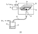
- FIG. 9 is a schematic view of a manufacturing apparatus used when forming the fine particle-containing layer according to the present embodiment.
- the substrate 50 in which the intrinsic amorphous semiconductor layer 14 is formed on one surface of the crystalline semiconductor layer 12 is prepared.
- the substrate 50 is fixed to the XYZ stage 54 in the deposition chamber 52.
- the XYZ stage 54 is connected to a heater power source 56 and is configured to heat the substrate 50 as necessary.
- the deposition chamber 52 includes a discharge valve 58 connected to a pump provided outside.
- the manufacturing apparatus 100 includes an aerosol chamber 60 in addition to the deposition chamber 52.
- the aerosol chamber 60 contains a mixture of semiconductor fine particles containing silicon nanoparticles 40 and monosilane gas in an aerosol state. Then, the aerosol mixture is ejected from the nozzle 64 toward the surface of the substrate 50 through the pipe 62.
- FIG. 10 is a diagram schematically showing the fine particle-containing layer formed on the substrate.
- the aerosol mixture ejected from the nozzle 64 is deposited on the substrate 50 as semiconductor fine particles 65 containing silicon nanoparticles 40 and amorphous silicon 66.
- the semiconductor fine particles 65 the surface of the silicon nanoparticles 40 is covered with the silicon oxynitride film 46 or the silicon nitride film 48 described above.
- the amorphous silicon 66 functions as a matrix of the fine particle-containing layer 16 (26).
- the film forming method according to the present embodiment mixes silane gas, which is a gas that is easily mixed uniformly with fine particles, and silicon nanoparticles, and sprays the mixture onto the substrate, whereby the silicon nanoparticles are sprayed on the substrate. Can be deposited. A part of the silane gas that is a carrier gas is formed as a matrix of the fine particle-containing layer.
- emitted from the nozzle 64 may be suppressed, or the board
- the present invention has been described with reference to each of the above-described embodiments, but the present invention is not limited to the above-described embodiments, and those in which the configurations of the embodiments are appropriately combined or replaced. Are also included in the present invention.
- the described embodiments can also be included in the scope of the present invention.
- 10 photoelectric conversion device 12 crystal semiconductor layer, 14 intrinsic amorphous semiconductor layer, 16 fine particle-containing layer, 16a silicon nanoparticle, 16b insulating film, 16c semiconductor fine particle, 18 first amorphous semiconductor layer, 20 transparent conductive film , 22 comb electrode, 24 intrinsic amorphous semiconductor layer, 26 fine particle-containing layer, 26a silicon nanoparticle, 26b insulating film, 26c semiconductor fine particle, 28 second amorphous semiconductor layer, 30 transparent conductive film, 32 comb electrode, 34 electrons, 36 holes, 38 silicon powder, 39 power supply, 40 silicon nanoparticles, 41, 42 platinum electrodes, 44 silicon oxide film, 46 silicon oxynitride film, 48 silicon nitride film.
- the present invention is suitable for solar cells and the like.
Landscapes
- Chemical & Material Sciences (AREA)
- Engineering & Computer Science (AREA)
- Nanotechnology (AREA)
- Physics & Mathematics (AREA)
- Life Sciences & Earth Sciences (AREA)
- Biophysics (AREA)
- Optics & Photonics (AREA)
- Crystallography & Structural Chemistry (AREA)
- Photovoltaic Devices (AREA)
Abstract
光電変換装置10は、一導電型の結晶半導体層12と、結晶半導体層の一方の面上に形成されている真性非晶質半導体層14と、真性非晶質半導体層の上に形成され、半導体微粒子を含有する微粒子含有層16と、微粒子含有層の上に形成されており、結晶半導体層に対して逆導電型の第1の非晶質半導体層18または結晶半導体層と同じ一導電型の非晶質半導体層と、を備える。半導体微粒子は、その粒径が4~7nmの範囲の粒子を含む。
Description
本発明は、太陽電池に好適な光電変換装置に関する。
従来、光エネルギーを電気エネルギーに変換する光電変換装置として、いわゆる太陽電池の開発が各方面で精力的に行われている。例えば、単結晶シリコンや多結晶シリコン等の結晶系シリコンを用いた太陽電池の研究および実用化が盛んに行われている。
また、近年、非晶質シリコンと結晶系シリコンとを組み合わせることにより構成されたヘテロ接合を有する太陽電池の開発も進んでいる。このタイプの太陽電池では、ヘテロ接合を200℃以下の低温プロセスで形成することができ、かつ、高い変換効率が得られることから、注目を集めている。
このようなタイプの太陽電池として、例えば、n型結晶シリコンの表面側にi型非晶質シリコン層とp型非晶質シリコン層とが積層され、裏面側にi型非晶質シリコン層とn型非晶質シリコン層とが積層されている構造が知られている(例えば、特許文献1参照)。
しかしながら、前述の太陽電池においては、p型、i型、n型非晶質シリコン中に局在準位が存在しているため、局在準位に起因するリーク電流が発生する。その結果、太陽電池の変換効率が低下する。
本発明はこうした状況に鑑みてなされたものであり、その目的とするところは、光電変換装置における変換効率を向上させる技術を提供することにある。
上記課題を解決するために、本発明のある態様の光電変換装置は、一導電型の結晶半導体層と、結晶半導体層の一方の面上に形成されている真性非晶質半導体層と、真性非晶質半導体層の上に形成され、半導体微粒子を含有する微粒子含有層と、微粒子含有層の上に形成されており、結晶半導体層に対して逆導電型の非晶質半導体層または結晶半導体層と同じ一導電型の非晶質半導体層と、を備える。半導体微粒子は、その粒径が4~7nmの範囲の粒子を含む。
本発明によれば、光電変換装置における変換効率を向上させることができる。
以下、図面を参照しながら、本発明を実施するための形態について詳細に説明する。なお、図面の説明において同一の要素には同一の符号を付し、重複する説明を適宜省略する。
図1は、本実施の形態に係る光電変換装置の断面図である。以下の各図に示す各層、各部の縮尺や形状は、説明を容易にするために便宜的に設定されており、特に言及がない限り限定的に解釈されるものではない。
図1に示すように、本実施の形態に係る光電変換装置10は、一導電型の結晶半導体層12と、結晶半導体層12の一方の面(図1に示す上面)上に形成されている真性非晶質半導体層14と、真性非晶質半導体層14の上に形成され、半導体微粒子を含有する微粒子含有層16と、微粒子含有層16の上に形成されており、結晶半導体層12に対して逆導電型の第1の非晶質半導体層18と、第1の非晶質半導体層18の上に形成されている透明導電膜20と、透明導電膜20の表面上の所定領域に形成されている櫛形電極22と、を備える。
また、光電変換装置10は、図1に示すように、結晶半導体層12の他方の面(図1に示す下面)上に形成されている真性非晶質半導体層24と、真性非晶質半導体層24の下に形成され、半導体微粒子を含有する微粒子含有層26と、微粒子含有層26の下に形成されており、結晶半導体層12と同じ一導電型の第2の非晶質半導体層28と、第2の非晶質半導体層28の下に形成されている透明導電膜30と、透明導電膜30の表面上の所定領域に形成されている櫛形電極32と、を備える。
以下、本実施の形態における各層について詳述する。結晶半導体層12は、n型単結晶シリコンである。本実施の形態に好適なn型単結晶シリコンは、抵抗率が約1Ω・cm、厚みが200~300μmである。真性非晶質半導体層14は、i型アモルファスシリコン(a-Si)半導体であり、公知のRFプラズマCVD(13.56MHz)法を用いて結晶半導体層12の上面に約10nmの厚みとなるように成膜されている。
微粒子含有層16は、後述する図2(a)に示すように、半導体微粒子16cを含む半導体層である。半導体微粒子16cは、その粒子のサイズ(粒径)が4~7nmの範囲のもののみで構成されていることが好ましい。但し、これに限らず、粒径の異なる粒子で構成されていてもよく、例えば、粒径分布のピークが4~7nmの範囲にある粒子群であってもよい。
半導体微粒子16cは、シリコンナノ粒子16aと、その周囲(表面)を覆う絶縁膜16bとで構成される。シリコンナノ粒子16aは、結晶質シリコンである単結晶シリコンまたは多結晶シリコンをナノレベルの粉末状(パウダー状)に作製したものであり、その粒子のサイズ(粒径)が2~3nmの範囲のもののみで構成されていることが好ましいが、これに限らず、粒径の異なる粒子で構成されていてもよく、例えば、粒径分布のピークが2~3nmの範囲にある粒子群であってもよい。絶縁膜16bは、シリコン酸化膜(SiO)、シリコン酸窒化膜(SiON)、シリコン窒化膜(SiN)などである。絶縁膜16bの厚みは、約1~2nmである。
微粒子含有層16は、例えば、後述するエアロゾル堆積法により真性非晶質半導体層14の上に約10~30nmの厚みとなるように成膜されている。
第1の非晶質半導体層18は、p型アモルファスシリコン(a-Si)半導体であり、公知のRFプラズマCVD法を用いて微粒子含有層16の上に約10nmの厚みとなるように成膜されている。透明導電膜20は、酸化インジウム(In2O3)に数%の酸化スズ(SnO2)が添加されているITO膜である。透明導電膜20は、公知のスパッタリング法を用いて第1の非晶質半導体層18の上に約100nmの厚みとなるように成膜されている。なお、光電変換装置10は、透明導電膜20が設けられている側が受光面となる。
櫛形電極22は、銀(Ag)からなる導電性フィラーと熱硬化性樹脂とを有している。櫛形電極22は、透明導電膜20の表面上の所定の領域に、フィンガー部とバスバー部とからなる所定のパターンが印刷により形成されている。
また、真性非晶質半導体層24は、i型アモルファスシリコン(a-Si)半導体であり、公知のRFプラズマCVD法を用いて結晶半導体層12の下面上に約10nmの厚みとなるように成膜されている。
微粒子含有層26は、後述する図2(a)に示すように、半導体微粒子26cを含む半導体層である。半導体微粒子26cは、その粒子のサイズ(粒径)が4~7nmの範囲のもののみで構成されていることが好ましい。但し、これに限らず、粒径の異なる粒子で構成されていてもよく、例えば、粒径分布のピークが4~7nmの範囲にある粒子群であってもよい。
半導体微粒子26cは、シリコンナノ粒子26aと、その周囲(表面)を覆う絶縁膜26bとで構成される。シリコンナノ粒子26aは、結晶質シリコンである単結晶シリコンまたは多結晶シリコンをナノレベルの粉末状(パウダー状)に作製したものであり、その粒子のサイズ(粒径)が2~3nmの範囲のもののみで構成されていることが好ましいが、これに限らず、粒径の異なる粒子で構成されていてもよく、例えば、粒径分布のピークが2~3nmの範囲にある粒子群であってもよい。絶縁膜16bは、シリコン酸化膜(SiO)、シリコン酸窒化膜(SiON)、シリコン窒化膜(SiN)などである。絶縁膜16bの厚みは、約1~2nmである。
微粒子含有層26は、例えば、後述するエアロゾル堆積法により真性非晶質半導体層24の下に約10~30nmの厚みとなるように成膜されている。
第2の非晶質半導体層28は、n型アモルファスシリコン(a-Si)半導体であり、公知のRFプラズマCVD法を用いて微粒子含有層26の下に約10nmの厚みとなるように成膜されている。透明導電膜30は、酸化インジウム(In2O3)に数%の酸化スズ(SnO2)が添加されているITO膜である。透明導電膜30は、公知のスパッタリング法を用いて第2の非晶質半導体層28の下に約100nmの厚みとなるように成膜されている。
櫛形電極32は、銀(Ag)からなる導電性フィラーと熱硬化性樹脂とを有している。櫛形電極32は、透明導電膜30の表面上の所定の領域に、フィンガー部とバスバー部とからなる所定のパターンが印刷により形成されている。
図2(a)は、本実施の形態に係る光電変換装置の層構造を模式的に示した図、図2(b)は、本実施の形態に係る光電変換装置のバンド図を模式的に示した図である。
従来の光電変換装置においては、p型a-Si層、i型a-Si層およびn型a-Si層は、多くの局在準位Lを含むため、そのままの状態では、リーク電流が流れやすくなる。そこで、本実施の形態に係る光電変換装置10は、i型a-Si層とp型a-Si層との間に、絶縁膜16bで覆われているシリコンナノ粒子16aを含む微粒子含有層16を挟み込んでいる。また、光電変換装置10は、i型a-Si層とn型a-Si層との間に、絶縁膜26bで覆われているシリコンナノ粒子26aを含む微粒子含有層26を挟み込んでいる。
図2(b)に示すEcは伝導体の下端のエネルギーを示し、Evは価電子帯の上端のエネルギーを示す。図2(b)に示すように、微粒子含有層16,26において、シリコンナノ粒子16aに起因するバンドギャップは狭くなっており、絶縁膜16bに起因するバンドギャップは広い。また、シリコンナノ粒子16aにより、井戸の底よりも高い位置に複数のミニバンドBが形成されている。
そのため、光電変換装置10は、半導体微粒子16cを構成するシリコンナノ粒子16aによって形成されたミニバンドにおけるエネルギー準位により、共鳴トンネルダイオードが形成されていることになる。すなわち、ミニバンドにおけるエネルギー準位と同程度のエネルギーを持った電子34(正孔36)だけがミニバンドを通過できる。シリコンナノ粒子16aの場合、ミニバンドBのバンドギャップは2eV程度であり、アモルファスシリコンの約1.7eVより大きい。そのため、アモルファスシリコン内の低い局在準位を伝わってp(n)型アモルファスシリコン層にキャリアが漏れ出ることが抑制される。
このように、キャリアが漏れ出ることが抑制されれば、光電変換装置(太陽電池)の特性を決める指標の一つである開放電圧Vocを大きくできる。太陽電池の変換効率ηは、式(1)で示される。
η∝Voc×Isc×FF・・・式(1)
Voc:開放電圧
Isc:短絡電流密度
FF:曲線因子
これにより、開放電圧Vocの増大により変換効率ηが向上する。
η∝Voc×Isc×FF・・・式(1)
Voc:開放電圧
Isc:短絡電流密度
FF:曲線因子
これにより、開放電圧Vocの増大により変換効率ηが向上する。
(シリコンナノ粒子の製造方法)
次に、シリコンナノ粒子の製造方法について詳述する。図3乃至図6は、本実施の形態に係るシリコンナノ粒子の製造方法を説明するための模式図である。この方法は、電気的にフローティング状態のシリコンパウダーをフッ酸(HF)+過酸化水素水(H2O2)の混合液でエッチングすることでシリコンナノ粒子を作製する際に、特定の波長より長い波長の光を照射する点が特徴の一つである。なお、混合液にメタノールを添加してもよい。
次に、シリコンナノ粒子の製造方法について詳述する。図3乃至図6は、本実施の形態に係るシリコンナノ粒子の製造方法を説明するための模式図である。この方法は、電気的にフローティング状態のシリコンパウダーをフッ酸(HF)+過酸化水素水(H2O2)の混合液でエッチングすることでシリコンナノ粒子を作製する際に、特定の波長より長い波長の光を照射する点が特徴の一つである。なお、混合液にメタノールを添加してもよい。
はじめに、シリコンを主成分とするシリコンパウダーを準備する。シリコンパウダーは、シリコン系排水処理装置から濃縮分離されたものであってもよい。このようなシリコンパウダーは、シリコン材料のリサイクルという観点からも好適である。次に、図3に示すように、シリコンパウダー38を、白金(Pt)電極とともに、HF+H2O2(+メタノール)混合液に浸漬する。この時点でのシリコンパウダー38の粒径は、数μmから数mmの大きさである。
ここで、周波数νの光のエネルギーEは、プランク定数をhとすると、以下に示す式(2)の関係を満たす。
E=hν(=hc/λ)・・・式(2)
c:光速
λ:光の波長
E=hν(=hc/λ)・・・式(2)
c:光速
λ:光の波長
したがって、シリコンパウダー38に照射される光のエネルギーEが、シリコンパウダー38におけるシリコンナノ粒子のバンドギャップEg’より大きい場合、その粒子では正孔が発生しエッチングが進行する。そこで、hν>Eg’となるように、照射光の波長を設定する。
更に光を照射し続けると、図4に示すように、シリコンナノ粒子40は、その表面がポーラス状にエッチングされ直径が徐々に小さくなる。シリコンナノ粒子40は、エッチングが進行し直径が小さくなると、直径に反比例してバンドギャップが大きくなる。つまり、エッチングされたシリコンナノ粒子のバンドギャップEg”は、エッチング前のシリコンナノ粒子のバンドギャップEg’よりも大きくなる。
そのため、図5に示すように、照射する光のエネルギー(hν)よりもバンドギャップEgが大きくなると、照射光によりホールが生成されなくなる。その結果、エッチングが自然に停止し、所望の粒径のシリコンナノ粒子40が得られる。
なお、粒径が2nmよりも小さいシリコンナノ粒子は、バンドギャップが大きいため、光電変換装置にはあまり適さない。一方、粒径が3nmよりも大きいシリコンナノ粒子は、バンドギャップが小さいため、半導体として十分な機能を発揮しない場合がある。そのため、シリコンナノ粒子の粒径は、約2~3nmの範囲が好適である。
例えば、所望の粒径のシリコンナノ粒子40のバンドギャップEgが約2.0eVの場合、2.0eV以下のエネルギーの光を照射する。具体的には、2eVのエネルギーに対応する波長620nm以上の光を照射する。なお、照射される光は、少なくともシリコンパウダー38におけるシリコンナノ粒子のバンドギャップEg’より大きなエネルギーを有している。これにより、シリコン粒子中に正孔が発生しエッチングが開始する。
つまり、本実施の形態に係る製造方法によれば、溶液に照射する光の波長によりシリコンナノ粒子の直径を制御できる。また、所望の粒径となったシリコンナノ粒子40は、負に帯電している。そこで、図6に示すように、電源39の負極側に白金電極41を、正極側に白金電極42を接続することで、正に帯電した白金電極42により容易に回収することができる。
(半導体微粒子の製造方法)
前述の工程で得られたシリコンナノ粒子は、その表面が水素終端されているが、室内に放置するだけで容易に酸化される。そこで、以下の工程によって、シリコンナノ粒子の表面に疎水性の保護膜を形成し、半導体微粒子とする。図7は、本実施の形態に係るシリコンナノ粒子に保護膜を形成する方法を説明するための模式図である。なお、保護膜は、先に述べたシリコンナノ粒子16aの表面を覆う絶縁膜16bに相当する。
前述の工程で得られたシリコンナノ粒子は、その表面が水素終端されているが、室内に放置するだけで容易に酸化される。そこで、以下の工程によって、シリコンナノ粒子の表面に疎水性の保護膜を形成し、半導体微粒子とする。図7は、本実施の形態に係るシリコンナノ粒子に保護膜を形成する方法を説明するための模式図である。なお、保護膜は、先に述べたシリコンナノ粒子16aの表面を覆う絶縁膜16bに相当する。
図7に示すように、水素終端されているシリコンナノ粒子40の表面を、酸素プラズマ処理またはオゾンアッシング処理により酸化してシリコン酸化膜44にする。その後、窒素プラズマ処理により窒化して、シリコン酸化膜44をシリコン酸窒化膜46にする。シリコン酸窒化膜46は、シリコン酸化膜44と比べると疎水性であり、シリコンナノ粒子40が大気中の水分により不必要に酸化されることが抑制される。また、前述の一連の処理は、シリコンナノ粒子を室温でウェット酸化する場合と比較して、短時間で行うことができる。なお、シリコン酸化膜44が表面に形成されたシリコンナノ粒子40を窒化せずに、前述した微粒子含有層16に含有させてもよい。
前述した通り、シリコンナノ粒子の粒径は、約2~3nmの範囲が好適であるが、実際に光電変換装置に適用する際には、その表面が約1~2nmの厚みの保護膜で覆われるので、半導体微粒子の粒径としては約4~7nmの範囲が好適となる。なお、シリコンナノ粒子が、その粒径分布のピークが2~3nmの範囲にある粒子群である場合には、半導体微粒子は、その粒径分布のピークが4~7nmの範囲にある粒子群が好適となる。
図8は、本実施の形態に係るシリコンナノ粒子に保護膜を形成する他の方法を説明するための模式図である。
図8に示すように、所望のXガス(Xは、例えば、O2、H2O)雰囲気中で、水素終端されているシリコンナノ粒子40にレーザー光を照射することで、過酸化を防止しつつ短時間でシリコンナノ粒子40の表面をシリコン酸化膜44にすることができる。その後、XガスとしてN2(またはNH3)ガスに置換した雰囲気で、表面がシリコン酸化膜44で被覆されているシリコンナノ粒子40にレーサー光を照射することで、シリコン酸化膜44をシリコン酸窒化膜46にする。前述のように、シリコン酸窒化膜46は、シリコン酸化膜44と比べると疎水性であり、シリコンナノ粒子40が大気中の水分により不必要に酸化されることが抑制される。また、前述の一連の処理は、シリコンナノ粒子を室温でウェット酸化する場合と比較して、短時間で行うことができる。
なお、はじめからN2(またはNH3)ガス雰囲気中で、水素終端されているシリコンナノ粒子40にレーザー光を照射することで、短時間でシリコンナノ粒子40の表面をシリコン窒化膜48にすることができる。シリコン窒化膜48も、疎水性であり、シリコンナノ粒子40が大気中の水分により酸化されることが抑制される。
(微粒子含有層の成膜方法)
次に、前述の製造方法により得られたシリコンナノ粒子を光電変換装置10における微粒子含有層16,26として成膜する方法の一例を説明する。
次に、前述の製造方法により得られたシリコンナノ粒子を光電変換装置10における微粒子含有層16,26として成膜する方法の一例を説明する。
図9は、本実施の形態に係る微粒子含有層を成膜する際に使用する製造装置の模式図である。はじめに、結晶半導体層12の一方の面上に真性非晶質半導体層14を成膜した基板50を準備する。次に、基板50は、堆積チャンバー52内のXYZステージ54に固定される。XYZステージ54は、ヒータ電源56に接続されており、必要に応じて基板50を加熱できるように構成されている。また、堆積チャンバー52は、外部に設けられているポンプと接続されている排出弁58を備えている。
また、製造装置100は、堆積チャンバー52とは別にエアロゾルチャンバー60を備えている。エアロゾルチャンバー60は、シリコンナノ粒子40を含有する半導体微粒子とモノシランガスとを混合した混合物をエアロゾル状態として収容している。そして、エアロゾル状態の混合物は、配管62を介してノズル64から基板50の表面に向かって射出される。
図10は、基板上に形成された微粒子含有層を模式的に示した図である。図10に示すように、ノズル64から射出されたエアロゾル状態の混合物は、シリコンナノ粒子40を含有する半導体微粒子65およびアモルファスシリコン66として基板50上に堆積される。半導体微粒子65は、シリコンナノ粒子40の表面が前述のシリコン酸窒化膜46やシリコン窒化膜48で覆われている。アモルファスシリコン66は、微粒子含有層16(26)のマトリックスとして機能する。
このように、本実施の形態に係る成膜方法は、微小な粒子と均一に混ざりやすい気体であるシランガスとシリコンナノ粒子とを混合し、その混合物を基板に吹き付けることでシリコンナノ粒子を基板上に堆積できる。また、キャリアガスであるシランガスの一部は、微粒子含有層のマトリックスとして成膜される。なお、混合物を吹き付ける際の基板へのダメージを抑制するために、ノズル64から射出される粒子の速度を抑えたり、基板50を加熱したりしてもよい。
以上、本発明を上述の各実施の形態を参照して説明したが、本発明は上述の実施の形態に限定されるものではなく、実施の形態の構成を適宜組み合わせたものや置換したものについても本発明に含まれるものである。また、当業者の知識に基づいて実施の形態における組合せや処理の順番を適宜組み替えることや各種の設計変更等の変形を実施の形態に対して加えることも可能であり、そのような変形が加えられた実施の形態も本発明の範囲に含まれうる。
10 光電変換装置、 12 結晶半導体層、 14 真性非晶質半導体層、 16 微粒子含有層、 16a シリコンナノ粒子、 16b 絶縁膜、 16c 半導体微粒子、 18 第1の非晶質半導体層、 20 透明導電膜、 22 櫛形電極、 24 真性非晶質半導体層、 26 微粒子含有層、 26a シリコンナノ粒子、 26b 絶縁膜、 26c 半導体微粒子、 28 第2の非晶質半導体層、 30 透明導電膜、 32 櫛形電極、 34 電子、 36 正孔、 38 シリコンパウダー、 39 電源、 40 シリコンナノ粒子、 41,42 白金電極、 44 シリコン酸化膜、 46 シリコン酸窒化膜、 48 シリコン窒化膜。
本発明は、太陽電池などに好適である。
Claims (5)
- 一導電型の結晶半導体層と、
前記結晶半導体層の一方の面上に形成されている真性非晶質半導体層と、
前記真性非晶質半導体層の上に形成され、半導体微粒子を含有する微粒子含有層と、
前記微粒子含有層の上に形成されており、前記結晶半導体層に対して逆導電型の非晶質半導体層または前記結晶半導体層と同じ一導電型の非晶質半導体層と、を備え、
前記半導体微粒子は、その粒径が4~7nmの範囲の粒子を含むことを特徴とする光電変換装置。 - 前記半導体微粒子は、シリコン粒子と、前記シリコン粒子の表面を覆う絶縁膜とを含むことを特徴とする請求項1に記載の光電変換装置。
- 前記結晶半導体層は、n型単結晶シリコンからなり、
前記逆導電型の非晶質半導体層を備える場合には、前記逆導電型の非晶質半導体層は、p型アモルファスシリコン半導体からなり、前記一導電型の非晶質半導体層を備える場合には、前記一導電型の非晶質半導体層はn型アモルファスシリコン半導体からなることを特徴とする請求項1または2に記載の光電変換装置。 - 前記半導体微粒子は、粒径分布のピークが4~7nmの範囲にある粒子群であることを特徴とする請求項1乃至3のいずれか1項に記載の光電変換装置。
- 前記結晶半導体層の他方の面上に形成されている他の真性非晶質半導体層と、
前記他の真性非晶質半導体層の上に形成され、半導体微粒子を含有する微粒子含有層と、
前記微粒子含有層の上に形成されており、前記結晶半導体層と同じ一導電型の非晶質半導体層または前記結晶半導体層に対して逆導電型の非晶質半導体層と、を備え、
前記半導体微粒子は、その粒径が4~7nmの範囲の粒子を含むことを特徴とする請求項1乃至4のいずれか1項に記載の光電変換装置。
Applications Claiming Priority (2)
| Application Number | Priority Date | Filing Date | Title |
|---|---|---|---|
| JP2011-077879 | 2011-03-31 | ||
| JP2011077879A JP2014116327A (ja) | 2011-03-31 | 2011-03-31 | 光電変換装置 |
Publications (1)
| Publication Number | Publication Date |
|---|---|
| WO2012131826A1 true WO2012131826A1 (ja) | 2012-10-04 |
Family
ID=46929669
Family Applications (1)
| Application Number | Title | Priority Date | Filing Date |
|---|---|---|---|
| PCT/JP2011/006887 Ceased WO2012131826A1 (ja) | 2011-03-31 | 2011-12-09 | 光電変換装置 |
Country Status (2)
| Country | Link |
|---|---|
| JP (1) | JP2014116327A (ja) |
| WO (1) | WO2012131826A1 (ja) |
Families Citing this family (2)
| Publication number | Priority date | Publication date | Assignee | Title |
|---|---|---|---|---|
| US8822262B2 (en) * | 2011-12-22 | 2014-09-02 | Sunpower Corporation | Fabricating solar cells with silicon nanoparticles |
| CN110741478B (zh) * | 2017-10-18 | 2023-08-29 | 汉阳大学校产学协力团 | 层、多级元件、多级元件制造方法和驱动多级元件的方法 |
Citations (6)
| Publication number | Priority date | Publication date | Assignee | Title |
|---|---|---|---|---|
| JP2006319335A (ja) * | 2005-05-12 | 2006-11-24 | General Electric Co <Ge> | 表面パシベーティッド光起電装置 |
| JP2007535806A (ja) * | 2004-04-30 | 2007-12-06 | ニューサウス・イノヴェイションズ・ピーティーワイ・リミテッド | 人工アモルファス半導体および太陽電池への適用 |
| JP2008533729A (ja) * | 2005-03-14 | 2008-08-21 | キュー−セルズ アーゲー | 太陽電池 |
| JP2010206004A (ja) * | 2009-03-04 | 2010-09-16 | Seiko Epson Corp | 光電変換装置および電子機器 |
| WO2011004446A1 (ja) * | 2009-07-06 | 2011-01-13 | トヨタ自動車株式会社 | 光電変換素子 |
| WO2011010379A1 (ja) * | 2009-07-23 | 2011-01-27 | トヨタ自動車株式会社 | 光電変換素子 |
-
2011
- 2011-03-31 JP JP2011077879A patent/JP2014116327A/ja not_active Withdrawn
- 2011-12-09 WO PCT/JP2011/006887 patent/WO2012131826A1/ja not_active Ceased
Patent Citations (6)
| Publication number | Priority date | Publication date | Assignee | Title |
|---|---|---|---|---|
| JP2007535806A (ja) * | 2004-04-30 | 2007-12-06 | ニューサウス・イノヴェイションズ・ピーティーワイ・リミテッド | 人工アモルファス半導体および太陽電池への適用 |
| JP2008533729A (ja) * | 2005-03-14 | 2008-08-21 | キュー−セルズ アーゲー | 太陽電池 |
| JP2006319335A (ja) * | 2005-05-12 | 2006-11-24 | General Electric Co <Ge> | 表面パシベーティッド光起電装置 |
| JP2010206004A (ja) * | 2009-03-04 | 2010-09-16 | Seiko Epson Corp | 光電変換装置および電子機器 |
| WO2011004446A1 (ja) * | 2009-07-06 | 2011-01-13 | トヨタ自動車株式会社 | 光電変換素子 |
| WO2011010379A1 (ja) * | 2009-07-23 | 2011-01-27 | トヨタ自動車株式会社 | 光電変換素子 |
Also Published As
| Publication number | Publication date |
|---|---|
| JP2014116327A (ja) | 2014-06-26 |
Similar Documents
| Publication | Publication Date | Title |
|---|---|---|
| Mariani et al. | Patterned radial GaAs nanopillar solar cells | |
| US10276738B2 (en) | Photovoltaic cell, including a crystalline silicon oxide passivation thin film, and method for producing same | |
| EP2782146B1 (en) | Method for manufacturing a solar cell with reduced potential induced degradation | |
| CN101884116A (zh) | 太阳能电池及其制造方法 | |
| US20110203650A1 (en) | Optical converter device and electronic equipment including the optical converter device | |
| US9761749B2 (en) | Photoelectric conversion device | |
| JP5919559B2 (ja) | 光起電力装置 | |
| CN103782394A (zh) | 太阳能电池和该太阳能电池的制造方法 | |
| CN108028290B (zh) | 光电转换元件 | |
| EP2822042A1 (en) | Photovoltaic device | |
| JP5826094B2 (ja) | p型半導体材料、および光電変換装置の作製方法 | |
| CN104362209B (zh) | 一种背面抛光晶硅太阳能电池及其制备工艺 | |
| JP2014116327A (ja) | 光電変換装置 | |
| KR101106480B1 (ko) | 광기전력 장치의 제조 방법 | |
| US20110017288A1 (en) | Thin film type solar cell and method of manufacturing the same | |
| KR20130035876A (ko) | 광전 변환 장치 | |
| US20150179843A1 (en) | Photovoltaic device | |
| WO2017010029A1 (ja) | 光電変換装置 | |
| CN105378938A (zh) | 太阳能电池的制造方法 | |
| CN101728447A (zh) | 太阳能装置及其制造方法 | |
| JP6206687B2 (ja) | 光起電力装置及びその製造方法 | |
| KR101368905B1 (ko) | 박막형 태양전지의 제조방법 | |
| JP2005244071A (ja) | 太陽電池およびその製造方法 | |
| KR102118905B1 (ko) | 터널 산화막을 포함하는 태양 전지 및 이의 제조 방법 | |
| CN107195694A (zh) | 硅基异质接面太阳能电池及其制作方法 |
Legal Events
| Date | Code | Title | Description |
|---|---|---|---|
| 121 | Ep: the epo has been informed by wipo that ep was designated in this application |
Ref document number: 11862725 Country of ref document: EP Kind code of ref document: A1 |
|
| NENP | Non-entry into the national phase |
Ref country code: DE |
|
| 122 | Ep: pct application non-entry in european phase |
Ref document number: 11862725 Country of ref document: EP Kind code of ref document: A1 |
|
| NENP | Non-entry into the national phase |
Ref country code: JP |