WO2012127938A1 - フレキシブルケーブルおよび媒体処理装置 - Google Patents
フレキシブルケーブルおよび媒体処理装置 Download PDFInfo
- Publication number
- WO2012127938A1 WO2012127938A1 PCT/JP2012/053446 JP2012053446W WO2012127938A1 WO 2012127938 A1 WO2012127938 A1 WO 2012127938A1 JP 2012053446 W JP2012053446 W JP 2012053446W WO 2012127938 A1 WO2012127938 A1 WO 2012127938A1
- Authority
- WO
- WIPO (PCT)
- Prior art keywords
- detection signal
- disconnection detection
- pattern
- signal pattern
- flexible cable
- Prior art date
- Legal status (The legal status is an assumption and is not a legal conclusion. Google has not performed a legal analysis and makes no representation as to the accuracy of the status listed.)
- Ceased
Links
Images


Classifications
-
- H—ELECTRICITY
- H05—ELECTRIC TECHNIQUES NOT OTHERWISE PROVIDED FOR
- H05K—PRINTED CIRCUITS; CASINGS OR CONSTRUCTIONAL DETAILS OF ELECTRIC APPARATUS; MANUFACTURE OF ASSEMBLAGES OF ELECTRICAL COMPONENTS
- H05K1/00—Printed circuits
- H05K1/02—Details
- H05K1/0275—Security details, e.g. tampering prevention or detection
-
- G—PHYSICS
- G11—INFORMATION STORAGE
- G11B—INFORMATION STORAGE BASED ON RELATIVE MOVEMENT BETWEEN RECORD CARRIER AND TRANSDUCER
- G11B17/00—Guiding record carriers not specifically of filamentary or web form, or of supports therefor
- G11B17/02—Details
- G11B17/04—Feeding or guiding single record carrier to or from transducer unit
- G11B17/0408—Feeding or guiding single record carrier to or from transducer unit of non-disc record carrier, e.g. card
-
- H—ELECTRICITY
- H01—ELECTRIC ELEMENTS
- H01B—CABLES; CONDUCTORS; INSULATORS; SELECTION OF MATERIALS FOR THEIR CONDUCTIVE, INSULATING OR DIELECTRIC PROPERTIES
- H01B7/00—Insulated conductors or cables characterised by their form
- H01B7/04—Flexible cables, conductors, or cords, e.g. trailing cables
-
- G—PHYSICS
- G01—MEASURING; TESTING
- G01R—MEASURING ELECTRIC VARIABLES; MEASURING MAGNETIC VARIABLES
- G01R31/00—Arrangements for testing electric properties; Arrangements for locating electric faults; Arrangements for electrical testing characterised by what is being tested not provided for elsewhere
- G01R31/50—Testing of electric apparatus, lines, cables or components for short-circuits, continuity, leakage current or incorrect line connections
- G01R31/52—Testing for short-circuits, leakage current or ground faults
-
- G—PHYSICS
- G06—COMPUTING OR CALCULATING; COUNTING
- G06K—GRAPHICAL DATA READING; PRESENTATION OF DATA; RECORD CARRIERS; HANDLING RECORD CARRIERS
- G06K19/00—Record carriers for use with machines and with at least a part designed to carry digital markings
- G06K19/06—Record carriers for use with machines and with at least a part designed to carry digital markings characterised by the kind of the digital marking, e.g. shape, nature, code
- G06K19/067—Record carriers with conductive marks, printed circuits or semiconductor circuit elements, e.g. credit or identity cards also with resonating or responding marks without active components
- G06K19/07—Record carriers with conductive marks, printed circuits or semiconductor circuit elements, e.g. credit or identity cards also with resonating or responding marks without active components with integrated circuit chips
- G06K19/077—Constructional details, e.g. mounting of circuits in the carrier
-
- H—ELECTRICITY
- H05—ELECTRIC TECHNIQUES NOT OTHERWISE PROVIDED FOR
- H05K—PRINTED CIRCUITS; CASINGS OR CONSTRUCTIONAL DETAILS OF ELECTRIC APPARATUS; MANUFACTURE OF ASSEMBLAGES OF ELECTRICAL COMPONENTS
- H05K1/00—Printed circuits
- H05K1/02—Details
- H05K1/0213—Electrical arrangements not otherwise provided for
- H05K1/0216—Reduction of cross-talk, noise or electromagnetic interference
- H05K1/0218—Reduction of cross-talk, noise or electromagnetic interference by printed shielding conductors, ground planes or power plane
-
- H—ELECTRICITY
- H05—ELECTRIC TECHNIQUES NOT OTHERWISE PROVIDED FOR
- H05K—PRINTED CIRCUITS; CASINGS OR CONSTRUCTIONAL DETAILS OF ELECTRIC APPARATUS; MANUFACTURE OF ASSEMBLAGES OF ELECTRICAL COMPONENTS
- H05K1/00—Printed circuits
- H05K1/02—Details
- H05K1/03—Use of materials for the substrate
- H05K1/0393—Flexible materials
Definitions
- the present invention relates to a data input / output contact for inputting and outputting data and a flexible cable connected to a plurality of contacts other than the data input / output contact.
- the present invention also relates to a medium processing apparatus including such a flexible cable.
- a flexible cable is connected to a plurality of IC contacts that contact the connection terminals of the IC card (see, for example, Patent Document 1).
- a power pattern, a ground pattern, a clock signal pattern, and a data signal pattern are formed on one surface of the flexible cable to reduce crosstalk between signals transmitted through the flexible cable.
- a shield pattern connected to the power supply pattern and the ground pattern is formed on the other surface of the cable.
- Patent Document 2 a flexible cable that can prevent unauthorized acquisition of data has been proposed (for example, see Patent Document 2).
- the flexible cable described in Patent Document 2 is connected to the signal terminal of the magnetic head.
- the upper and lower surfaces of the signal wiring layer on which the data signal pattern for sending the data signal from the magnetic head is formed are covered with the protective layer.
- the protective layer a disconnection detection pattern having a disconnection detection function and a short circuit detection pattern are formed. Therefore, in the flexible cable described in Patent Document 2, it is possible to prevent a signal line for illegal data acquisition from being attached to the data signal pattern, and as a result, prevent unauthorized acquisition of data from the flexible cable. It becomes possible.
- the flexible cable described in Patent Document 1 can reduce crosstalk between signals transmitted through the flexible cable.
- this flexible cable it is difficult to prevent unauthorized acquisition of data from the flexible cable.
- the flexible cable described in Patent Document 2 it is possible to prevent unauthorized acquisition of data from the flexible cable.
- crosstalk increases due to the influence of a disconnection detection pattern or a short circuit detection pattern.
- an object of the present invention is to provide a flexible cable capable of achieving both prevention of illegal acquisition of data and reduction of crosstalk. Moreover, the subject of this invention is providing the medium processing apparatus provided with this flexible cable.
- the flexible cable of the present invention is a data input / output contact for inputting and / or outputting data and a flexible cable connected to a plurality of contacts other than the data input / output contact.
- a data signal pattern connected to an output contact and a data signal layer formed with a plurality of signal patterns connected to a plurality of contacts, and a disconnection detection for covering the surface of the data signal layer and detecting the disconnection of itself A first disconnection detection signal layer in which a disconnection detection signal pattern for transmitting a signal is formed, and a disconnection detection signal pattern for covering the rear surface of the data signal layer and transmitting a disconnection detection signal for detecting the disconnection of itself are formed.
- a second disconnection detection signal layer and a first disconnection detection signal layer and / or a second disconnection detection In the signal layer, a shield pattern is formed at a position avoiding the disconnection detection signal pattern, and the data signal pattern is covered with the disconnection detection signal pattern of the first disconnection detection signal layer and the disconnection detection signal pattern of the second disconnection detection signal layer.
- the signal pattern is formed such that at least a part thereof avoids the disconnection detection signal pattern of the first disconnection detection signal layer and / or the second disconnection detection signal layer in which the shield pattern is formed. It is characterized by that.
- the data signal pattern connected to the data input / output contact is formed to be covered with the disconnection detection signal pattern of the first disconnection detection signal layer and the disconnection detection signal pattern of the second disconnection detection signal layer.
- a shield pattern is formed at a position avoiding the disconnection detection signal pattern, and the signal is connected to a contact other than the data input / output contact. At least a part of the pattern is formed so as to avoid the disconnection detection signal pattern of the first disconnection detection signal layer and / or the second disconnection detection signal layer in which the shield pattern is formed. Therefore, in this embodiment, crosstalk can be reduced by the action of the shield pattern formed in the first disconnection detection signal layer or the second disconnection detection signal layer. That is, with the flexible cable of the present invention, it is possible to achieve both prevention of illegal acquisition of data and reduction of crosstalk.
- a clock signal pattern for transmitting a clock signal is formed as a signal pattern in the data signal layer, and a signal pattern excluding the clock signal pattern is formed so that at least a part thereof is covered with a shield pattern, It is preferable that at least a part of the clock signal pattern is formed so as to avoid the shield pattern.
- the flexible cable is formed in an elongated shape in one direction, and the disconnection detection signal pattern of the first disconnection detection signal layer and / or the second disconnection detection signal layer in which the shield pattern is formed is
- the clock signal pattern is formed on one end side in the width direction and the other end portion in the width direction of the flexible cable. If comprised in this way, the distance of the data signal pattern formed so that it may be covered with the disconnection detection signal pattern of a 1st disconnection detection signal layer and the disconnection detection signal pattern of a 2nd disconnection detection signal layer, and a clock signal pattern Can be released. Therefore, it is possible to reduce the noise of the data signal due to the clock signal.
- the flexible cable includes a data input / output contact and a contact connection portion connected to the plurality of contacts, and the area of the contact connection portion is larger than the area of the data input / output contact and the plurality of contact arrangement regions. It is preferable. If comprised in this way, it will become possible to cover a data input / output contact completely by a contact connection part. Therefore, it becomes possible to prevent the data input / output contact from being attached with a signal line for illegal data acquisition by the contact connecting portion.
- a disconnection detection signal pattern is formed in the entire area of either the first disconnection detection signal layer or the second disconnection detection signal layer in the contact connection portion.
- the flexible cable is preferably formed in a long and narrow shape in one direction, and the disconnection detection signal pattern is preferably formed by being folded back multiple times in the width direction of the flexible cable.
- the disconnection detection signal pattern is easily disconnected when the disconnection detection signal layer is cut in an attempt to attach the signal line for illegal data acquisition to the data signal pattern. Therefore, it becomes easy to detect criminal acts by criminals.
- the first disconnection detection signal layer and the second disconnection detection signal layer are formed with a short circuit detection signal pattern for transmitting a short circuit detection signal for detecting a short circuit with the disconnection detection signal pattern.
- a short circuit detection signal pattern for transmitting a short circuit detection signal for detecting a short circuit with the disconnection detection signal pattern.
- the flexible cable of the present invention can be used in a medium processing apparatus having a data input / output contact and a plurality of contacts.
- this medium processing apparatus it is possible to achieve both prevention of unauthorized acquisition of data from the flexible cable and reduction of crosstalk in the flexible cable.
- the flexible cable is formed so as to be connected to the data input / output contact and the plurality of contacts, and to be connected to the contact connection, so as to cover at least a connection portion between the data input / output contact and the contact connection. It is preferable to provide a terminal cover portion that is folded back and fixed to the contact connection portion. If comprised in this way, it will become possible to prevent that the signal wire
- the first disconnection detection signal layer and / or the second disconnection detection signal layer includes a first disconnection detection signal pattern which is a disconnection detection signal pattern on the input side of the disconnection detection signal and an output side of the disconnection detection signal.
- a second disconnection detection signal pattern that is a disconnection detection signal pattern is formed, and a land for connecting the first disconnection detection signal pattern and the second disconnection detection signal pattern is formed in the contact connection portion and the terminal cover portion,
- the medium processing apparatus includes a connector to which a flexible cable is connected, and the disconnection detection signal pattern has a function of detecting disconnection of the flexible cable from the connector.
- the flexible cable of the present invention it is possible to achieve both prevention of illegal acquisition of data and reduction of crosstalk.
- the medium processing apparatus of the present invention it is possible to achieve both prevention of unauthorized acquisition of data from the flexible cable and reduction of crosstalk in the flexible cable.
- FIG. 5 is a cross-sectional view taken along a line EE in FIG. 4.
- FIG. 5 is a sectional view taken along the line FF in FIG. 4.
- FIG. 4 is a cross-sectional view taken along a line GG in FIG. 3.
- It is a block diagram which shows the connection relation of the signal pattern in the flexible cable shown in FIG. It is sectional drawing of the connection part of IC contact and flexible cable concerning other embodiment of this invention.
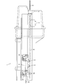
- FIG. 1 is a side view for explaining a schematic configuration of a medium processing apparatus 1 according to an embodiment of the present invention.
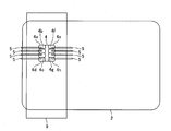
- FIG. 2 is a plan view showing a state where the IC contact 5 is in contact with the card 2 shown in FIG.
- the medium processing apparatus 1 of this embodiment is a card reader that reads data recorded on a card 2 that is a recording medium and writes data to the card 2.
- the medium processing apparatus 1 is a so-called dip type card reader in which the user manually inserts the card 2 into the apparatus and removes the card 2 from the apparatus.
- the medium processing apparatus 1 is mounted and used in a predetermined host apparatus.
- the medium processing apparatus 1 includes a magnetic head 3 that reads magnetic data recorded on the card 2 and eight IC contacts 5 that contact a terminal portion 4 formed on the card 2.
- a flexible cable 6 is connected to the plurality of IC contacts 5. Further, a card passage 8 through which the card 2 passes is formed inside the medium processing apparatus 1.
- Card 2 is, for example, a rectangular vinyl chloride card having a thickness of about 0.7 to 0.8 mm.
- a magnetic stripe on which magnetic data is recorded is formed on one surface of the card 2.
- a terminal portion 4 is formed on the other surface of the card 2. That is, the card 2 of the present embodiment is a contact IC card with a magnetic stripe.
- the card 2 may include a communication antenna.
- the card 2 may be a PET (polyethylene terephthalate) card having a thickness of about 0.18 to 0.36 mm, or a paper card having a predetermined thickness.
- the terminal section 4 includes eight connection terminals 4a to 4h as shown in FIG.
- the connection terminal 4a is a power supply terminal
- the connection terminal 4b is a reset signal terminal
- the connection terminal 4c is a clock signal terminal
- the connection terminal 4e is a ground (ground) terminal.
- the connection terminal 4f is a program power supply terminal
- the connection terminal 4g is a data input / output terminal for inputting / outputting data.
- the connection terminals 4d and 4h are spare terminals.
- the magnetic head 3 is arranged so that its magnetic gap faces the card passage 8. In this embodiment, when the user inserts the card 2 into the apparatus or pulls out the card 2 inserted into the apparatus, the magnetic data of the card 2 is read by the magnetic head 3.
- the IC contact 5 is disposed on the back end side of the medium processing apparatus 1 and is positioned and held by the IC contact block 9.
- a lever member 10 and a tension coil spring (not shown) that biases the IC contact block 9 toward the insertion side of the card 2 are attached to the IC contact block 9.
- the lever member 10 rotates and each of the eight IC contacts 5 is connected to the connection terminals 4a to 4a.
- the IC contact block 9 moves so as to contact 4h.
- data can be exchanged between the medium processing apparatus 1 and the card 2.
- the IC contact block 9 is moved by the urging force of the tension coil spring, and the IC contact 5 is retracted from the card passage 8.
- the IC contact 5 that contacts the connection terminal 4g is a data input / output contact for inputting / outputting data
- the other IC contacts 5 are contacts other than the data input / output contact.
- One end side of the flexible cable 6 is connected to eight IC contacts 5, and the other end side of the flexible cable 6 is connected to a connector (not shown) provided in a host device on which the medium processing apparatus 1 is mounted. Yes.
- This connector is mounted in an area of the host device where security is ensured.
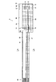
- FIG. 3 is a plan view of the flexible cable 6 shown in FIG.
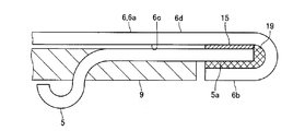
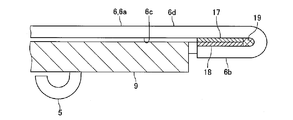
- FIG. 4 is a plan view of a connection portion between the IC contact 5 and the flexible cable 6 shown in FIG. 5 is a cross-sectional view taken along the line EE of FIG. 6 is a cross-sectional view taken along the line FF of FIG. 7 is a cross-sectional view taken along the line GG in FIG.
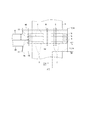
- FIG. 8 is a block diagram showing a connection relationship of signal patterns in the flexible cable 6 shown in FIG.
- the flexible cable 6 is formed in a long and narrow shape in one direction.
- the flexible cable 6 includes a contact connection portion 6a in which eight contact lands 15 connected to the IC contact 5 are formed, and an IC contact 5 and a contact that contact the connection terminals 4e to 4h. And a folded portion 6b as a terminal cover portion which is folded back so as to cover the connection portion with the land 15 and fixed to the contact connection portion 6a.
- a connection terminal portion 16 connected to a connector of the host device is formed on one end side in the longitudinal direction of the flexible cable 6.
- the contact connection portion 6 a is formed on the other end side in the longitudinal direction of the flexible cable 6. Further, the contact connecting portion 6a is formed in a rectangular shape. As described above, eight contact lands 15 are formed in the contact connecting portion 6a. The eight contact lands 15 are formed on the surface 6 c of the flexible cable 6. The contact land 15 is soldered to the IC contact terminal 5a (see FIG. 5) of the IC contact 5 protruding from the IC contact block 9 in the longitudinal direction of the flexible cable 6, and the contact land 15 is connected to the IC contact terminal 5a. Is soldered to fix the flexible cable 6 to the plurality of IC contacts 5.
- the folded portion 6 b is formed so as to be connected to the contact connection portion 6 a in the longitudinal direction of the flexible cable 6.
- a land 17 is formed near the boundary between the contact connecting portion 6a and the folded portion 6b of the contact connecting portion 6a, and a land is formed near the boundary between the contact connecting portion 6a and the folded portion 6b of the folded portion 6b.
- 18 is formed. Specifically, lands 17 are formed on both ends of the contact connection portion 6a in the width direction orthogonal to the longitudinal direction of the flexible cable 6, and lands are formed on both ends of the folded portion 6b in the width direction of the flexible cable 6. 18 is formed.
- the folded portion 6b covers the connection portion between the IC contact terminal 5a of the IC contact 5 that contacts the connection terminals 4e to 4h and the contact land 15 from the IC contact terminal 5a side (that is, It is folded back (covered from the lower side of FIG. 5) and fixed to the contact connecting portion 6a.
- the land 17 and the land 18 overlap as shown in FIG. In this embodiment, the land 17 and the land 18 are soldered, and the folded portion 6b is fixed to the contact connection portion 6a.
- an adhesive 19 is applied between the contact connecting portion 6a and the folded portion 6b, and the folded portion 6b is also fixed to the contact connecting portion 6a by the adhesive 19.
- the width of the contact connecting portion 6a and the width of the folded portion 6b are equal. Further, in the width direction of the flexible cable 6, the contact connection portion 6 a and the folded portion 6 b are wider than the other portions of the flexible cable 6. As shown in FIG. 4, in the width direction of the flexible cable 6, the contact connecting portion 6 a is wider than the width of the arrangement region R of the eight IC contacts 5. Further, in the longitudinal direction of the flexible cable 6, the contact connecting portion 6 a is wider than the width of the arrangement region R of the IC contact 5. That is, the area of the contact connection portion 6 a is larger than the area of the arrangement region R of the IC contact 5. Further, the contact connecting portion 6 a completely covers the entire arrangement region R of the IC contact 5.
- the flexible cable 6 is formed in a multilayer structure including a data signal layer 23, disconnection detection signal layers 24 and 25, and an insulating layer 26.
- the insulating layer 26, the disconnection detection signal layer 24, the insulating layer 26, the data signal layer 23, the insulating layer 26, the disconnection detection signal layer 25, and the insulating layer 26 from the front surface 6 c to the back surface 6 d of the flexible cable 6. are stacked in this order. That is, the surface of the data signal layer 23 is covered with the disconnection detection signal layer 24 via the insulating layer 26, and the back surface of the data signal layer 23 is covered with the disconnection detection signal layer 25 via the insulating layer 26.
- the disconnection detection signal layer 24 of this embodiment is a first disconnection detection signal layer
- the disconnection detection signal layer 25 is a second disconnection detection signal layer.
- the data signal layer 23 is formed with a data signal pattern 27 (see FIG. 8) for transmitting a data signal from the IC contact 5 that contacts the connection terminal 4g to a host device on which the medium processing device 1 is mounted.
- One end of the data signal pattern 27 is connected to the IC contact 5 that contacts the connection terminal 4 g via the contact land 15, and the other end of the data signal pattern 27 is a data input / output terminal formed on the connection terminal portion 16. 28.
- no through hole to which the data signal pattern 27 is connected is formed.
- the data signal layer 23 has a power supply pattern 29 (see FIG. 8) in which one end is connected to the IC contact 5 that contacts the connection terminal 4a via the contact land 15 and an IC contact that contacts the connection terminal 4b. 5, a reset signal pattern 30 (see FIG. 8) whose one end is connected via the contact land 15 and a clock whose one end is connected via the contact land 15 to the IC contact 5 which contacts the connection terminal 4c.
- a signal pattern 31 (see FIG. 8), a spare pattern 32 (see FIG. 8) whose one end is connected to the IC contact 5 that contacts the connection terminal 4d via the contact land 15, and an IC that contacts the connection terminal 4e.
- a ground pattern 33 (see FIG. 8) whose one end is connected to the contact 5 via the contact land 15 and an IC contact 5 that contacts the connection terminal 4f via the contact land 15 Are connected to the IC contact 5 that contacts the connection terminal 4h via the contact land 15 and a spare pattern 35 (see FIG. 8). ing.
- the other end of the power supply pattern 29 is connected to a power supply terminal 39 formed on the connection terminal portion 16, and the other end of the reset signal pattern 30 is connected to a reset signal terminal 40 formed on the connection terminal portion 16,
- the other end of the clock signal pattern 31 is connected to a clock signal terminal 41 formed on the connection terminal portion 16, and the other end of the spare pattern 32 is connected to a spare terminal 42 formed on the connection terminal portion 16.
- the other end of the ground pattern 33 is connected to a ground terminal 43 formed on the connection terminal portion 16, and the other end of the program power supply pattern 34 is connected to a program power supply terminal 44 formed on the connection terminal portion 16.
- the other end of the spare pattern 35 is connected to a spare terminal 45 formed on the connection terminal portion 16.
- a disconnection detection signal pattern 47 (see FIG. 8) is formed in the disconnection detection signal layers 24 and 25.
- the disconnection detection signal pattern 47 transmits a disconnection detection signal for detecting that the disconnection detection signal pattern 47 itself is disconnected in order to prevent the signal line for skimming from being attached to the data signal pattern 27.
- the disconnection detection signal pattern 47 is formed by being folded back multiple times in the width direction of the flexible cable 6 and is formed in a substantially net shape as a whole. In the disconnection detection signal layer 24, the disconnection detection signal pattern 47 is formed in the whole area.
- a disconnection detection signal pattern 47 is formed in a part thereof, and a shield pattern is formed at a position avoiding the disconnection detection signal pattern 47. That is, in the disconnection detection signal layer 25, as shown in FIG. 3, a disconnection detection region 48 where the disconnection detection signal pattern 47 is formed and a shield region 49 where the shield pattern is formed are formed. Further, a non-shield region 50 in which no shield pattern is formed is formed in a part of the shield region 49.
- the disconnection detection region 48 is formed on one end side in the width direction of the flexible cable 6, and the shield region 49 is formed on the other end side in the width direction of the flexible cable 6.
- the disconnection detection region 48 and the shield region 49 are formed so that the area of the disconnection detection region 48 is larger than the area of the shield region 49. That is, in the contact connection portion 6a and the folded portion 6b, the width of the disconnection detection region 48 in the width direction of the flexible cable 6 is wider than the width of the shield region 49, except for a part thereof.
- the disconnection detection region 48 and the shield region 49 are formed so that the area of the disconnection detection region 48 and the area of the shield region 49 are substantially equal. Has been. That is, in the portion of the flexible cable 6 other than the contact connection portion 6a and the folded portion 6b, the width of the disconnection detection region 48 and the width of the shield region 49 in the width direction of the flexible cable 6 are equal.
- the disconnection detection area 48 includes all of the seven contact lands 15 other than the contact lands 15 connected to the IC contact 5 that contacts the connection terminals 4d and the connection terminals when viewed from the thickness direction of the flexible cable 6. It is formed so as to overlap with a part of the contact land 15 connected to the IC contact 5 in contact with 4d. Further, in the longitudinal direction of the flexible cable 6, the shield region 49 extends to one end side in the width direction of the flexible cable 6 on one end side of the contact connection portion 6 a opposite to the side where the folded portion 6 b is formed. The shield region 49 is formed in a substantially L shape when viewed from the thickness direction of the flexible cable 6. On one end side of the contact connection portion 6a, the width of the disconnection detection region 48 and the width of the shield region 49 in the width direction of the flexible cable 6 are equal.
- the non-shield region 50 is formed at the other end in the width direction of the flexible cable 6. Further, the non-shield region 50 is formed in the longitudinal direction of the flexible cable 6 in which the connection terminal portion 16 is formed from the boundary portion between the contact connection portion 6a and a portion of the flexible cable 6 other than the contact connection portion 6a and the folded portion 6b. It is formed to one end.
- the width of the non-shield region 50 in the width direction of the flexible cable 6 is a width that covers one signal pattern.
- the data signal pattern 27 is routed in the disconnection detection region 48 when viewed from the thickness direction of the flexible cable 6. That is, the data signal pattern 27 is formed so as to be covered with the disconnection detection signal pattern 47 of the disconnection detection signal layer 24 and the disconnection detection signal pattern 47 of the disconnection detection signal layer 25.
- the seven signal patterns 29 to 35 other than the data signal pattern 27 are except for one end side of the signal patterns 29 to 35 connected to the contact land 15 when viewed from the thickness direction of the flexible cable 6.
- the outside of the disconnection detection area 48 is routed around. That is, the signal patterns 29 to 35 are formed so as to avoid the disconnection detection signal pattern 47 of the disconnection detection signal layer 25.
- the power supply pattern 29, the reset signal pattern 30, the spare pattern 32, the ground pattern 33, the program power supply pattern 34, and the spare pattern 35 have their back surfaces except their one end connected to the contact land 15. It is formed so as to be covered with the shield region 49 (that is, covered with the shield pattern).
- the clock signal pattern 31 for transmitting the clock signal is covered with a shield region 49 of the contact connection portion 6a except for one end thereof connected to the contact land 15, and most of the back surface. Is formed so as to be covered with the non-shield region 50. That is, most of the clock signal pattern 31 is formed so as to avoid the shield pattern, and the other end portion of the flexible cable 6 in the width direction of the flexible cable 6 other than the contact connecting portion 6a and the folded portion 6b. Is formed.
- the disconnection detection signal layers 47 are formed in the disconnection detection signal layers 24 and 25.
- the disconnection detection signal pattern 47 As the disconnection detection signal pattern 47, the disconnection detection signal pattern 47A on the input side of the disconnection detection signal and the disconnection detection signal pattern 47B on the output side of the disconnection detection signal are formed in the disconnection detection signal layers 24 and 25. Yes.
- the disconnection detection signal pattern 47A of the present embodiment is a first disconnection detection signal pattern, and the disconnection detection signal pattern 47B is a second disconnection detection signal pattern.
- one end of the disconnection detection signal pattern 47A is connected to one land 17 of the contact connection portion 6a, and the other end of the disconnection detection signal pattern 47A is a disconnection formed in the connection terminal portion 16. It is connected to the detection terminal 52.
- One end of the disconnection detection signal pattern 47B is connected to the other land 17 of the contact connection portion 6a, and the other end of the disconnection detection signal pattern 47B is connected to the disconnection detection terminal 53 formed in the connection terminal portion 16. Yes.
- One land 18 and the other land 18 formed in the folded portion 6 b are connected to each other by an inter-land signal pattern 54.
- one end of the disconnection detection signal pattern 47A may be connected to one land 18 of the folded portion 6b, and one end of the disconnection detection signal pattern 47B may be connected to the other land 18 of the folded portion 6b.
- one land 17 and the other land 17 of the contact connecting portion 6a are connected to each other by the inter-land signal pattern.
- the disconnection detection terminal 52 and the disconnection detection terminal 53 are electrically connected via the disconnection detection signal patterns 47A and 47B, the lands 17 and 18 and the inter-land signal pattern 54.
- the lands 17 and 18 and the inter-land signal pattern 54 connect the disconnection detection signal pattern 47A and the disconnection detection signal pattern 47B so that the disconnection detection signal patterns 47A and 47B function.
- disconnection detection signal patterns 47A and 47B are used to detect the disconnection of the flexible cable 6 from the connector.
- a short circuit detection signal pattern 55 (see FIG. 8) is formed.
- the short circuit detection signal pattern 55 transmits a short circuit detection signal for detecting a short circuit between the disconnection detection signal pattern 47 and the short circuit detection signal pattern 55.
- one end of the short circuit detection signal pattern 55 is connected to the short circuit detection terminal 56 formed on the connection terminal portion 16, and the other end of the short circuit detection signal pattern 55 is formed on the connection terminal portion 16.
- the short circuit detection terminal 57 is connected.
- the data signal pattern 27 is covered with the disconnection detection signal pattern 47 of the disconnection detection signal layer 24 and the disconnection detection signal pattern 47 of the disconnection detection signal layer 25. Is formed. Therefore, when a criminal tries to attach a signal line for acquiring data fraud to the data signal pattern 27, it is possible to detect that a criminal act is being performed using the disconnection detection signal pattern 47. Further, the through hole to which the data signal pattern 27 is connected is not formed in the flexible cable 6 of this embodiment. Therefore, in this embodiment, it is possible to prevent the signal line for illegally acquiring data from being attached to the data signal pattern 27, and as a result, it is possible to prevent unauthorized acquisition of data from the flexible cable 6. .
- the power supply pattern 29, the reset signal pattern 30, the spare pattern 32, the ground pattern 33, the program power supply pattern 34, and the spare pattern 35 are on the back surfaces except for one end side connected to the contact land 15. Therefore, the crosstalk can be reduced by the action of the shield pattern formed in the shield region 49. That is, in this embodiment, it is possible to achieve both prevention of illegal acquisition of data and reduction of crosstalk.
- most of the clock signal pattern 31 is formed so as to be covered with the non-shield region 50. For this reason, in this embodiment, it is possible to increase the rising speed and falling speed of the clock signal transmitted through the clock signal pattern 31 to suppress the rounding of the clock signal waveform.
- the disconnection detection signal pattern 47 of the disconnection detection signal layer 25 is formed on one end side in the width direction of the flexible cable 6, and the clock signal pattern 31 is formed on the other end portion in the width direction of the flexible cable 6.
- the data signal pattern 27 formed so as to be covered by the disconnection detection signal pattern 47 of the disconnection detection signal layer 25 is formed on one end side in the width direction of the flexible cable 6, and the clock signal pattern 31 is The flexible cable 6 is formed at the other end in the width direction.
- the distance between the data signal pattern 27 and the clock signal pattern 31 can be increased. Therefore, in this embodiment, it is possible to reduce the noise of the data signal due to the clock signal.
- the area of the contact connection portion 6a is larger than the area of the arrangement region R of the IC contact 5, and the contact connection portion 6a completely covers the entire area of the arrangement region R of the IC contact 5.
- the folded portion 6b is folded back so as to cover the connection portion between the IC contact terminal 5a of the IC contact 5 that contacts the connection terminals 4e to 4h and the contact land 15 and is fixed to the contact connection portion 6a.
- the contact contact portion 6a and the turn-back portion 6b connect the IC contact 5 that contacts the connection terminal 4g and the connection between the IC contact terminal 5a of the IC contact 5 that contacts the connection terminal 4g and the contact land 15. The part can be completely covered.
- the signal connection line for data fraud acquisition is attached to the IC contact 5 that contacts the connection terminal 4g by the contact connection portion 6a and the turn-back portion 6b, and the IC contact 5 that contacts the connection terminal 4g. It is possible to prevent a signal line for illegal data acquisition from being attached to a connection portion between the IC contact terminal 5a and the contact connection portion 6a.
- the disconnection detection signal pattern 47 is formed in the entire area of the disconnection detection signal layer 24. For this reason, the disconnection detection signal pattern 47 is easily disconnected when the flexible cable 6 is disconnected in order to attach the signal line for illegal data acquisition to the IC contact 5 that contacts the connection terminal 4g. Further, in this embodiment, the disconnection detection signal pattern 47 is formed by being folded back multiple times in the width direction of the flexible cable 6, and is formed in a substantially net shape as a whole, so that the IC contact 5 that contacts the connection terminal 4g. When the disconnection detection signal layers 24 and 25 are cut in order to attach a signal line for illegal data acquisition to the data signal pattern 27, the disconnection detection signal pattern 47 is easily disconnected. Therefore, in this embodiment, it becomes easy to detect criminal acts by criminals.
- the disconnection detection signal pattern 47A and the disconnection detection signal pattern 47B are connected by the land 17 of the contact connecting portion 6a and the land 18 of the folded portion 6b, which are fixed by soldering, and the inter-land signal pattern 54. ing. Therefore, when the folded portion 6b is peeled off from the contact connection portion 6a, the disconnection of the disconnection detection signal pattern 47 is detected. Therefore, in this embodiment, it becomes possible to detect criminal acts by criminals at an early stage.
- a short-circuit detection signal pattern 55 that transmits a short-circuit detection signal for detecting a short-circuit with the disconnection detection signal pattern 47 is formed in the disconnection detection region 48 and the disconnection detection signal layer 24 of the disconnection detection layer 25. Yes. Therefore, in order to prevent the disconnection detection signal from functioning, when a criminal performs a predetermined work on the disconnection detection signal pattern 47, a criminal act is performed by the short-circuit detection function of the short-circuit detection signal pattern 55. It becomes possible to detect this. That is, in this embodiment, it becomes easy to detect criminal acts by criminals.
- the disconnection detection signal pattern 47 it is possible to detect disconnection of the flexible cable 6 from the connector using the disconnection detection signal pattern 47. Therefore, when the criminal tries to attach the signal line for skimming to the data signal pattern 27 and pulls out the flexible cable 6 from the connector, the criminal act is performed by the disconnection detection signal pattern 47 disconnection detection function. Can be detected. Therefore, in this embodiment, it becomes possible to detect criminal acts by criminals at an early stage.
- the contact land 15 is formed in the contact connecting portion 6a, and the contact land 15 is soldered to the IC contact terminal 5a of the IC contact 5 protruding from the IC contact block 9 in the longitudinal direction of the flexible cable 6. ing.
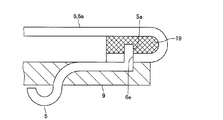
- a through hole 6 e is formed in the contact connecting portion 6 a, and the IC contact terminal 5 a of the IC contact 5 protruding from the IC contact block 9 in the thickness direction of the flexible cable 6. May be inserted into the through hole 6e and soldered.
- the contact connecting portion 6a is folded back so as to cover the IC contact terminal 5a of the IC contact 5 inserted through the through hole 6e. Further, the folded portion of the contact connecting portion 6 a is fixed by the adhesive 19. In this case, the folded portion 6 b is not formed on the flexible cable 6.
- a shield pattern is formed on the disconnection detection signal layer 25.
- a shield pattern may be formed in the disconnection detection signal layer 24.
- shield patterns may be formed on both the disconnection detection signal layer 24 and the disconnection detection signal layer 25.
- the data signal pattern 27 includes the disconnection detection signal pattern 47 of the disconnection detection signal layer 24 and the disconnection detection signal layer 25. It is formed so as to be covered with the disconnection detection signal pattern 47.
- the medium processing apparatus 1 is a dip type card reader in which the user manually inserts the card 2 into the apparatus and removes it from the apparatus.
- the medium processing apparatus to which the configuration of the present invention is applied may be a card transport type card reader provided with a card transport mechanism.
- the medium processing apparatus to which the configuration of the present invention is applied may be an apparatus other than a card reader.
- the flexible cable 6 is connected to the plurality of IC contacts 5, but the flexible cable 6 may be connected to data input / output contacts and contacts other than the IC contacts 5.
- the flexible cable 6 may be connected to a data input / output contact and a contact of a SAM socket to which a SAM (Secure Application Module) for authenticating a non-contact IC card is connected.
- SAM Secure Application Module
Landscapes
- Engineering & Computer Science (AREA)
- Computer Security & Cryptography (AREA)
- Microelectronics & Electronic Packaging (AREA)
- Insulated Conductors (AREA)
- Structure Of Printed Boards (AREA)
- Cable Accessories (AREA)
- Details Of Connecting Devices For Male And Female Coupling (AREA)
Abstract
データの不正取得の防止とクロストークの低減とを両立させることが可能なフレキシブルケーブルを提供する。 フレキシブルケーブル6は、データ入出力接点に接続されるデータ信号パターン27およびデータ入出力接点以外の接点に接続される信号パターン31が形成されるデータ信号層と、データ信号層の表面および裏面を覆うとともに自身が断線したことを検知するための断線検知信号を伝える断線検知信号パターンが形成される2個の断線検知信号層を備える多層構造に形成され、2個の断線検知信号層の少なくとも一方では、断線検知信号パターンを避けた位置にシールドパターンが形成されている。データ信号パターン27は、2個の断線検知信号層の断線検知信号パターンに覆われるように形成され、信号パターン31は、少なくともその一部が、シールドパターンが形成される断線検知信号層の断線検知信号パターンを避けるように形成されている。
Description
本発明は、データの入力や出力を行うためのデータ入出力接点およびデータ入出力接点以外の複数の接点に接続されるフレキシブルケーブルに関する。また、本発明は、かかるフレキシブルケーブルを備える媒体処理装置に関する。
従来、接触式のICカードとデータのやりとりを行うカードリーダが広く利用されている。この種のカードリーダでは、ICカードの接続端子に接触する複数のIC接点にフレキシブルケーブルが接続されている(たとえば、特許文献1参照)。特許文献1に記載のフレキシブルケーブルでは、フレキシブルケーブルを伝わる信号間のクロストークを低減するため、フレキシブルケーブルの一方の面に、電源パターン、グランドパターン、クロック信号パターンおよびデータ信号パターンが形成され、フレキシブルケーブルの他方の面に電源パターンおよびグランドパターンに繋がるシールドパターンが形成されている。
また、カードリーダが利用される業界においては、従来、犯罪者がカードに記録されたデータを不正に取得するデータの不正取得が大きな問題となっている。そこで、従来、データの不正取得を防止することが可能なフレキシブルケーブルが提案されている(たとえば、特許文献2参照)。特許文献2に記載のフレキシブルケーブルは、磁気ヘッドの信号端子に接続されている。このフレキシブルケーブルでは、磁気ヘッドからのデータ信号が送られるデータ信号パターンが形成された信号配線層の上下両面は、保護層によって覆われている。保護層には、断線検出機能を有する断線検出パターンと、短絡検出パターンとが形成されている。そのため、特許文献2に記載のフレキシブルケーブルでは、データ信号パターンにデータ不正取得用の信号線が取り付けられるのを防止することが可能になり、その結果、フレキシブルケーブルからのデータの不正取得を防止することが可能になる。
上述のように、特許文献1に記載のフレキシブルケーブルでは、フレキシブルケーブルを伝わる信号間のクロストークを低減することが可能である。しかしながら、このフレキシブルケーブルでは、フレキシブルケーブルからのデータの不正取得を防止することが困難である。一方、特許文献2に記載のフレキシブルケーブルでは、フレキシブルケーブルからのデータの不正取得を防止することが可能である。しかしながら、このフレキシブルケーブルをICカード用のカードリーダに用いた場合、断線検出パターンや短絡検出パターンの影響でクロストークが増加してしまう。
そこで、本発明の課題は、データの不正取得の防止とクロストークの低減とを両立させることが可能なフレキシブルケーブルを提供することにある。また、本発明の課題は、かかるフレキシブルケーブルを備える媒体処理装置を提供することにある。
上記の課題を解決するため、本発明のフレキシブルケーブルは、データの入力および/または出力を行うためのデータ入出力接点およびデータ入出力接点以外の複数の接点に接続されるフレキシブルケーブルにおいて、データ入出力接点に接続されるデータ信号パターンおよび複数の接点に接続される複数の信号パターンが形成されるデータ信号層と、データ信号層の表面を覆うとともに自身が断線したことを検知するための断線検知信号を伝える断線検知信号パターンが形成される第1断線検知信号層と、データ信号層の裏面を覆うとともに自身が断線したことを検知するための断線検知信号を伝える断線検知信号パターンが形成される第2断線検知信号層とを備える多層構造に形成され、第1断線検知信号層および/または第2断線検知信号層では、断線検知信号パターンを避けた位置にシールドパターンが形成され、データ信号パターンは、第1断線検知信号層の断線検知信号パターンと第2断線検知信号層の断線検知信号パターンとに覆われるように形成され、信号パターンは、少なくともその一部が、シールドパターンが形成される第1断線検知信号層および/または第2断線検知信号層の断線検知信号パターンを避けるように形成されていることを特徴とする。
本発明のフレキシブルケーブルでは、データ入出力接点に接続されるデータ信号パターンは、第1断線検知信号層の断線検知信号パターンと第2断線検知信号層の断線検知信号パターンとに覆われるように形成されている。そのため、犯罪者がデータ信号パターンへデータ不正取得用の信号線を取り付けようとしたときに、犯罪行為が行われていることを断線検知信号パターンを用いて検知することが可能になる。したがって、本発明では、データ信号パターンへのデータ不正取得用の信号線の取付を防止することが可能になり、その結果、フレキシブルケーブルからのデータの不正取得を防止することが可能になる。
また、本発明では、第1断線検知信号層および/または第2断線検知信号層では、断線検知信号パターンを避けた位置にシールドパターンが形成され、データ入出力接点以外の接点に接続される信号パターンは、少なくともその一部が、シールドパターンが形成される第1断線検知信号層および/または第2断線検知信号層の断線検知信号パターンを避けるように形成されている。そのため、本形態では、第1断線検知信号層や第2断線検知信号層に形成されるシールドパターンの作用でクロストークを低減することが可能になる。すなわち、本発明のフレキシブルケーブルでは、データの不正取得の防止とクロストークの低減とを両立させることが可能になる。
本発明において、データ信号層には、信号パターンとして、クロック信号を伝えるクロック信号パターンが形成され、クロック信号パターンを除く信号パターンは、少なくともその一部が、シールドパターンに覆われるように形成され、クロック信号パターンは、少なくともその一部が、シールドパターンを避けるように形成されていることが好ましい。このように構成すると、クロストークを低減しつつ、クロック信号の立上り速度および立下り速度を速くして、クロック信号波形のなまりを抑制することが可能になる。
本発明において、フレキシブルケーブルは、一方向へ細長い長尺状に形成され、シールドパターンが形成される第1断線検知信号層および/または第2断線検知信号層の断線検知信号パターンは、フレキシブルケーブルの幅方向の一端側に形成され、クロック信号パターンは、フレキシブルケーブルの幅方向の他端部に形成されていることが好ましい。このように構成すると、第1断線検知信号層の断線検知信号パターンと第2断線検知信号層の断線検知信号パターンとに覆われるように形成されるデータ信号パターンと、クロック信号パターンとの距離を離すことが可能になる。したがって、クロック信号に起因するデータ信号のノイズを低減することが可能になる。
本発明において、フレキシブルケーブルは、データ入出力接点および複数の接点に接続される接点接続部を備え、接点接続部の面積は、データ入出力接点および複数の接点の配置領域の面積よりも広くなっていることが好ましい。このように構成すると、接点接続部によって、データ入出力接点を完全に覆うことが可能になる。したがって、接点接続部によって、データ入出力接点にデータ不正取得用の信号線が取り付けられるのを防止することが可能になる。
本発明において、接点接続部における第1断線検知信号層または第2断線検知信号層のいずれか一方の全域に断線検知信号パターンが形成されていることが好ましい。このように構成すると、データ不正取得用の信号線をデータ入出力接点に取り付けようとして、フレキシブルケーブルを切ったときに、断線検知信号パターンが断線しやすくなる。したがって、犯罪者による犯罪行為を検知しやすくなる。
本発明において、フレキシブルケーブルは、一方向へ細長い長尺状に形成され、断線検知信号パターンは、フレキシブルケーブルの幅方向で複数回折り返されて形成されていることが好ましい。このように構成すると、データ不正取得用の信号線をデータ信号パターンに取り付けようとして、断線検知信号層を切ったときに、断線検知信号パターンが断線しやすくなる。したがって、犯罪者による犯罪行為を検知しやすくなる。
本発明において、第1断線検知信号層および第2断線検知信号層には、断線検知信号パターンとの間の短絡を検知するための短絡検知信号を伝える短絡検知信号パターンが形成されていることが好ましい。このように構成すると、断線検知信号が機能しないようにするために犯罪者が断線検知信号パターンに所定の細工を行った場合に、短絡検知信号パターンの短絡検知機能によって、犯罪行為が行われていることを検知することが可能になる。
本発明のフレキシブルケーブルは、データ入出力接点および複数の接点を備える媒体処理装置に用いることができる。この媒体処理装置では、フレキシブルケーブルからのデータの不正取得の防止とフレキシブルケーブルでのクロストークの低減とを両立させることが可能になる。
本発明において、フレキシブルケーブルは、データ入出力接点および複数の接点に接続される接点接続部と、接点接続部に繋がるように形成され少なくともデータ入出力接点と接点接続部との接続部分を覆うように折り返されて接点接続部に固定される端子覆部とを備えることが好ましい。このように構成すると、データ入出力接点と接点接続部との接続部分にデータ不正取得用の信号線が取り付けられるのを端子覆部によって防止することが可能になる。
本発明において、第1断線検知信号層および/または第2断線検知信号層には、断線検知信号の入力側の断線検知信号パターンである第1断線検知信号パターンと、断線検知信号の出力側の断線検知信号パターンである第2断線検知信号パターンとが形成され、接点接続部および端子覆部には、第1断線検知信号パターンと第2断線検知信号パターンとを繋げるためのランドが形成され、端子覆部のランドが接点接続部のランドに半田付けされることで、端子覆部が接点接続部に固定され、端子覆部のランドが接点接続部のランドに半田付けされると、第1断線検知信号パターンと第2断線検知信号パターンとが繋がることが好ましい。このように構成すると、接点接続部から端子覆部を剥がしにくくなる。したがって、データ入出力接点と接点接続部との接続部分にデータ不正取得用の信号線が取り付けられるのを効果的に防止することが可能になる。また、この場合には、接点接続部から端子覆部が剥がされると、端子覆部のランドが接点接続部のランドから離れるため、接点接続部から端子覆部が剥がされたときに、断線検知信号パターンの断線を検知することが可能になる。したがって、犯罪者による犯罪行為を早期に検知することが可能になる。
本発明において、媒体処理装置は、フレキシブルケーブルが接続されるコネクタを備え、断線検知信号パターンは、コネクタからのフレキシブルケーブルの抜けを検知する機能を果たしていることが好ましい。このように構成すると、犯罪者がデータ不正取得用の信号線をデータ信号パターンに取り付けようとして、フレキシブルケーブルをコネクタから引き抜いた場合に、断線検知信号パターンの抜け検知機能によって、犯罪行為が行われていることを検知することが可能になる。したがって、犯罪者による犯罪行為を早期に検知することが可能になる。
以上のように、本発明のフレキシブルケーブルでは、データの不正取得の防止とクロストークの低減とを両立させることが可能になる。また、本発明の媒体処理装置では、フレキシブルケーブルからのデータの不正取得の防止とフレキシブルケーブルでのクロストークの低減とを両立させることが可能になる。
以下、図面を参照しながら、本発明の実施の形態を説明する。
(媒体処理装置の概略構成)
図1は、本発明の実施の形態にかかる媒体処理装置1の概略構成を説明するための側面図である。図2は、図1に示すカード2にIC接点5が接触している状態を示す平面図である。
図1は、本発明の実施の形態にかかる媒体処理装置1の概略構成を説明するための側面図である。図2は、図1に示すカード2にIC接点5が接触している状態を示す平面図である。
本形態の媒体処理装置1は、記録媒体であるカード2に記録されたデータの読取りやカード2へのデータの書込みを行うカードリーダである。具体的には、媒体処理装置1は、ユーザが手動でカード2を装置内部に挿入するとともに装置内部から抜き取るいわゆるディップ式のカードリーダである。この媒体処理装置1は、所定の上位装置に搭載されて使用される。
媒体処理装置1は、カード2に記録された磁気データの読取りを行う磁気ヘッド3と、カード2に形成される端子部4に接触する8個のIC接点5とを備えている。複数のIC接点5には、フレキシブルケーブル6が接続されている。また、媒体処理装置1の内部には、カード2が通過するカード通過路8が形成されている。
カード2は、たとえば、厚さが0.7~0.8mm程度の矩形状の塩化ビニール製のカードである。このカード2の一方の面には、磁気データが記録される磁気ストライプが形成されている。また、カード2の他方の面には、端子部4が形成されている。すなわち、本形態のカード2は、磁気ストライプ付きの接触式ICカードである。なお、カード2には、通信用のアンテナが内蔵されても良い。また、カード2は、厚さが0.18~0.36mm程度のPET(ポリエチレンテレフタレート)カードであっても良いし、所定の厚さの紙カード等であっても良い。
端子部4は、図2に示すように、8個の接続端子4a~4hを備えている。接続端子4aは、電源用の端子であり、接続端子4bは、リセット信号用の端子であり、接続端子4cは、クロック信号用の端子であり、接続端子4eは、接地(グランド)用の端子であり、接続端子4fは、プログラム電源用の端子であり、接続端子4gは、データの入出力を行うためのデータ入出力用の端子である。また、接続端子4d、4hは、予備用の端子である。
磁気ヘッド3は、その磁気ギャップがカード通過路8に臨むように配置されている。本形態では、ユーザが装置内部へカード2を差し込む際、あるいは、装置内部に差し込まれたカード2を引き抜く際に、磁気ヘッド3によって、カード2の磁気データが読み取られる。
IC接点5は、媒体処理装置1の奥端側に配置されており、IC接点ブロック9に位置決めされて保持されている。IC接点ブロック9には、たとえば、レバー部材10と、カード2の挿入側に向かってIC接点ブロック9を付勢する引張りコイルバネ(図示省略)とが取り付けられている。本形態では、IC接点ブロック9の奥端に形成されるカード当接部9aにカード2が当接すると、レバー部材10が回動して、8個のIC接点5のそれぞれが接続端子4a~4hに接触するように、IC接点ブロック9が移動する。端子部4にIC接点5が接触すると、媒体処理装置1とカード2との間で、データのやりとりが可能になる。また、この状態でカード2が引き抜かれると、引張りコイルバネの付勢力で、IC接点ブロック9が移動して、IC接点5がカード通過路8から退避する。本形態では、接続端子4gに接触するIC接点5は、データの入出力を行うためのデータ入出力接点であり、その他のIC接点5は、データ入出力接点以外の接点である。
フレキシブルケーブル6の一端側は、8個のIC接点5に接続され、フレキシブルケーブル6の他端側は、媒体処理装置1が搭載される上位装置に設けられたコネクタ(図示省略)に接続されている。このコネクタは、上位装置の、セキュリティ性が確保された領域に実装されている。以下、フレキシブルケーブル6、および、IC接点5とフレキシブルケーブル6との接続部の構成について説明する。
(フレキシブルケーブルの構成、IC接点とフレキシブルケーブルとの接続部の構成)
図3は、図1に示すフレキシブルケーブル6の平面図である。図4は、図1に示すIC接点5とフレキシブルケーブル6との接続部の平面図である。図5は、図4のE-E断面の断面図である。図6は、図4のF-F断面の断面図である。図7は、図3のG-G断面の断面図である。図8は、図1に示すフレキシブルケーブル6内の信号パターンの接続関係を示すブロック図である。
図3は、図1に示すフレキシブルケーブル6の平面図である。図4は、図1に示すIC接点5とフレキシブルケーブル6との接続部の平面図である。図5は、図4のE-E断面の断面図である。図6は、図4のF-F断面の断面図である。図7は、図3のG-G断面の断面図である。図8は、図1に示すフレキシブルケーブル6内の信号パターンの接続関係を示すブロック図である。
フレキシブルケーブル6は、一方向へ細長い長尺状に形成されている。このフレキシブルケーブル6は、図3に示すように、IC接点5に接続される8個の接点用ランド15が形成される接点接続部6aと、接続端子4e~4hに接触するIC接点5と接点用ランド15との接続部分を覆うように折り返されて接点接続部6aに固定される端子覆部としての折返し部6bとを備えている。また、フレキシブルケーブル6の長手方向の一端側には、上位装置のコネクタに接続される接続端子部16が形成されている。
接点接続部6aは、フレキシブルケーブル6の長手方向の他端側に形成されている。また、接点接続部6aは、長方形状に形成されている。接点接続部6aには、上述のように、8個の接点用ランド15が形成されている。8個の接点用ランド15は、フレキシブルケーブル6の表面6cに形成されている。接点用ランド15は、フレキシブルケーブル6の長手方向において、IC接点ブロック9から突出するIC接点5のIC接点端子5a(図5参照)に半田付けされており、IC接点端子5aに接点用ランド15が半田付けされることで、複数のIC接点5にフレキシブルケーブル6が固定されている。
折返し部6bは、フレキシブルケーブル6の長手方向で接点接続部6aに繋がるように形成されている。接点接続部6aの、接点接続部6aと折返し部6bとの境界の近傍には、ランド17が形成され、折返し部6bの、接点接続部6aと折返し部6bとの境界の近傍には、ランド18が形成されている。具体的には、フレキシブルケーブル6の長手方向に直交する幅方向における接点接続部6aの両端側のそれぞれにランド17が形成され、フレキシブルケーブル6の幅方向における折返し部6bの両端側のそれぞれにランド18が形成されている。
折返し部6bは、図5に示すように、接続端子4e~4hに接触するIC接点5のIC接点端子5aと接点用ランド15との接続部分をIC接点端子5a側から覆うように(すなわち、図5の下側から覆うように)折り返されて、接点接続部6aに固定されている。折返し部6bが折り返されると、図6に示すようにランド17とランド18とが重なる。本形態では、ランド17とランド18とが半田付けされて、折返し部6bが接点接続部6aに固定されている。また、接点接続部6aと折返し部6bとの間には、接着剤19が塗布されており、接着剤19によっても、折返し部6bが接点接続部6aに固定されている。
フレキシブルケーブル6の幅方向において、接点接続部6aの幅と折返し部6bの幅とは、等しくなっている。また、フレキシブルケーブル6の幅方向において、接点接続部6aおよび折返し部6bの幅は、フレキシブルケーブル6の他の部分の幅よりも広くなっている。図4に示すように、フレキシブルケーブル6の幅方向において、接点接続部6aの幅は、8個のIC接点5の配置領域Rの幅よりも広くなっている。また、フレキシブルケーブル6の長手方向において、接点接続部6aの幅は、IC接点5の配置領域Rの幅よりも広くなっている。すなわち、接点接続部6aの面積は、IC接点5の配置領域Rの面積よりも大きくなっている。また、接点接続部6aは、IC接点5の配置領域Rの全域を完全に覆っている。
フレキシブルケーブル6は、図7に示すように、データ信号層23と、断線検知信号層24、25と、絶縁層26とを備える多層構造に形成されている。フレキシブルケーブル6では、フレキシブルケーブル6の表面6cから裏面6dに向かって、絶縁層26、断線検知信号層24、絶縁層26、データ信号層23、絶縁層26、断線検知信号層25および絶縁層26がこの順番に積層されている。すなわち、データ信号層23の表面は、絶縁層26を介して断線検知信号層24に覆われ、データ信号層23の裏面は、絶縁層26を介して断線検知信号層25に覆われている。本形態の断線検知信号層24は、第1断線検知信号層であり、断線検知信号層25は、第2断線検知信号層である。
データ信号層23には、接続端子4gに接触するIC接点5からのデータ信号を媒体処理装置1が搭載される上位装置へ伝えるデータ信号パターン27(図8参照)が形成されている。データ信号パターン27の一端は、接点用ランド15を介して接続端子4gに接触するIC接点5に接続され、データ信号パターン27の他端は、接続端子部16に形成されるデータ入出力用端子28に接続されている。なお、本形態のフレキシブルケーブル6には、データ信号パターン27が接続されるスルーホールは形成されていない。
また、データ信号層23には、データ信号パターン27以外に7本の信号パターンが形成されている。すなわち、データ信号層23には、接続端子4aに接触するIC接点5に接点用ランド15を介してその一端が接続される電源パターン29(図8参照)と、接続端子4bに接触するIC接点5に接点用ランド15を介してその一端が接続されるリセット信号パターン30(図8参照)と、接続端子4cに接触するIC接点5に接点用ランド15を介してその一端が接続されるクロック信号パターン31(図8参照)と、接続端子4dに接触するIC接点5に接点用ランド15を介してその一端が接続される予備パターン32(図8参照)と、接続端子4eに接触するIC接点5に接点用ランド15を介してその一端が接続されるグランドパターン33(図8参照)と、接続端子4fに接触するIC接点5に接点用ランド15を介してその一端が接続されるプログラム電源パターン34(図8参照)と、接続端子4hに接触するIC接点5に接点用ランド15を介してその一端が接続される予備パターン35(図8参照)とが形成されている。
電源パターン29の他端は、接続端子部16に形成される電源用端子39に接続され、リセット信号パターン30の他端は、接続端子部16に形成されるリセット信号用端子40に接続され、クロック信号パターン31の他端は、接続端子部16に形成されるクロック信号用端子41に接続され、予備パターン32の他端は、接続端子部16に形成される予備用端子42に接続されている。また、グランドパターン33の他端は、接続端子部16に形成されるグランド用端子43に接続され、プログラム電源パターン34の他端は、接続端子部16に形成されるプログラム電源用端子44に接続され、予備パターン35の他端は、接続端子部16に形成される予備用端子45に接続されている。
断線検知信号層24、25には、断線検知信号パターン47(図8参照)が形成されている。断線検知信号パターン47は、データ信号パターン27へのスキミング用の信号線の取付を防止するため、断線検知信号パターン47自身が断線したことを検知するための断線検知信号を伝えている。この断線検知信号パターン47は、フレキシブルケーブル6の幅方向に複数回折り返されて形成されており、全体として略網状に形成されている。断線検知信号層24では、その全域に断線検知信号パターン47が形成されている。
一方、断線検知信号層25では、その一部に断線検知信号パターン47が形成されており、断線検知信号パターン47を避けた位置にシールドパターンが形成されている。すなわち、断線検知信号層25には、図3に示すように、断線検知信号パターン47が形成される断線検知領域48と、シールドパターンが形成されるシールド領域49とが形成されている。また、シールド領域49の一部には、シールドパターンが形成されていない非シールド領域50が形成されている。
断線検知領域48は、フレキシブルケーブル6の幅方向の一端側に形成され、シールド領域49は、フレキシブルケーブル6の幅方向の他端側に形成されている。接点接続部6aおよび折返し部6bでは、断線検知領域48の面積がシールド領域49の面積よりも大きくなるように、断線検知領域48およびシールド領域49が形成されている。すなわち、接点接続部6aおよび折返し部6bでは、その一部分を除いて、フレキシブルケーブル6の幅方向における断線検知領域48の幅は、シールド領域49の幅よりも広くなっている。
また、フレキシブルケーブル6の、接点接続部6aおよび折返し部6b以外の部分では、断線検知領域48の面積とシールド領域49の面積とがほぼ等しくなるように、断線検知領域48およびシールド領域49が形成されている。すなわち、フレキシブルケーブル6の、接点接続部6aおよび折返し部6b以外の部分では、フレキシブルケーブル6の幅方向における断線検知領域48の幅とシールド領域49の幅とが等しくなっている。
断線検知領域48は、フレキシブルケーブル6の厚さ方向から見たときに、接続端子4dに接触するIC接点5に接続される接点用ランド15以外の7個の接点用ランド15の全部および接続端子4dに接触するIC接点5に接続される接点用ランド15の一部と重なるように形成されている。また、フレキシブルケーブル6の長手方向において、折返し部6bが形成される側の反対側となる接点接続部6aの一端側では、シールド領域49は、フレキシブルケーブル6の幅方向の一端側に広がるように形成されており、フレキシブルケーブル6の厚さ方向から見たときに、シールド領域49は、略L形状に形成されている。接点接続部6aの一端側では、フレキシブルケーブル6の幅方向における断線検知領域48の幅とシールド領域49の幅とが等しくなっている。
非シールド領域50は、フレキシブルケーブル6の幅方向の他端部に形成されている。また、非シールド領域50は、フレキシブルケーブル6の、接点接続部6aおよび折返し部6b以外の部分と接点接続部6aとの境界部から、接続端子部16が形成されるフレキシブルケーブル6の長手方向の一端まで形成されている。フレキシブルケーブル6の幅方向における非シールド領域50の幅は、1本の信号パターンを覆う程度の幅となっている。
データ信号パターン27は、図3に示すように、フレキシブルケーブル6の厚さ方向から見たときに、断線検知領域48内で引き回されている。すなわち、データ信号パターン27は、断線検知信号層24の断線検知信号パターン47と、断線検知信号層25の断線検知信号パターン47とに覆われるように形成されている。
一方、データ信号パターン27以外の7本の信号パターン29~35は、フレキシブルケーブル6の厚さ方向から見たときに、接点用ランド15に接続される信号パターン29~35の一端側を除いて、断線検知領域48の外側を引き回されている。すなわち、信号パターン29~35は、断線検知信号層25の断線検知信号パターン47を避けるように形成されている。
具体的には、電源パターン29、リセット信号パターン30、予備パターン32、グランドパターン33、プログラム電源パターン34および予備パターン35は、接点用ランド15に接続されるその一端側を除いて、その裏面がシールド領域49に覆われるように(すなわち、シールドパターンに覆われるように)形成されている。また、クロック信号を伝えるクロック信号パターン31は、接点用ランド15に接続されるその一端側を除いて、その裏面の一部分が接点接続部6aのシールド領域49に覆われるとともに、その裏面の大半部分が非シールド領域50に覆われるように形成されている。すなわち、クロック信号パターン31の大半部分は、シールドパターンを避けるように形成されており、フレキシブルケーブル6の、接点接続部6aおよび折返し部6b以外の部分では、フレキシブルケーブル6の幅方向の他端部に形成されている。
上述のように、断線検知信号層24、25には、断線検知信号パターン47が形成されている。本形態では、断線検知信号パターン47として、断線検知信号の入力側の断線検知信号パターン47Aと、断線検知信号の出力側の断線検知信号パターン47Bとが断線検知信号層24、25に形成されている。本形態の断線検知信号パターン47Aは、第1断線検知信号パターンであり、断線検知信号パターン47Bは、第2断線検知信号パターンである。
図8に示すように、断線検知信号パターン47Aの一端は、接点接続部6aの一方のランド17に接続されており、断線検知信号パターン47Aの他端は、接続端子部16に形成される断線検知端子52に接続されている。断線検知信号パターン47Bの一端は、接点接続部6aの他方のランド17に接続されており、断線検知信号パターン47Bの他端は、接続端子部16に形成される断線検知端子53に接続されている。折返し部6bに形成される一方のランド18と他方のランド18とは、ランド間信号パターン54によって互いに接続されている。なお、断線検知信号パターン47Aの一端が、折返し部6bの一方のランド18に接続され、断線検知信号パターン47Bの一端が、折返し部6bの他方のランド18に接続されても良い。この場合には、接点接続部6aの一方のランド17と他方のランド17とがランド間信号パターンによって互いに接続される。
上述のように、ランド17とランド18とが半田付けされ、また、2個のランド18間は、ランド間信号パターン54によって接続されている。そのため、断線検知端子52と断線検知端子53とは、断線検知信号パターン47A、47B、ランド17、18およびランド間信号パターン54を介して電気的に接続されている。本形態では、断線検知端子52を介して上位装置から入力される断線検知信号が断線検知端子53を介して上位装置へ戻らないと、断線検知信号パターン47A、47Bが断線したことが検知される。このように、本形態では、ランド17、18およびランド間信号パターン54は、断線検知信号パターン47A、47Bが機能するように、断線検知信号パターン47Aと断線検知信号パターン47Bとを繋いでいる。
また、上位装置に設けられたコネクタからフレキシブルケーブル6が抜けていると、上位装置からフレキシブルケーブル6へ断線検知信号が入力されず、その結果、上位装置へ断線検知信号が戻らない。そのため、本形態では、断線検知信号パターン47A、47Bを利用して、コネクタからのフレキシブルケーブル6の抜けを検知することもできる。すなわち、断線検知信号パターン47A、47Bは、コネクタからのフレキシブルケーブル6の抜けを検知する機能も果たしている。
また、断線検知層25の断線検知領域48および断線検知信号層24には、短絡検知信号パターン55(図8参照)が形成されている。短絡検知信号パターン55は、断線検知信号パターン47と短絡検知信号パターン55との間の短絡を検知するための短絡検知信号を伝えている。図8に示すように、短絡検知信号パターン55の一端は、接続端子部16に形成される短絡検知端子56に接続され、短絡検知信号パターン55の他端は、接続端子部16に形成される短絡検知端子57に接続されている。
(本形態の主な効果)
以上説明したように、本形態のフレキシブルケーブル6では、データ信号パターン27は、断線検知信号層24の断線検知信号パターン47と、断線検知信号層25の断線検知信号パターン47とに覆われるように形成されている。そのため、犯罪者がデータ信号パターン27へデータ不正取得用の信号線を取り付けようとしたときに、犯罪行為が行われていることを断線検知信号パターン47を用いて検知することが可能になる。また、本形態のフレキシブルケーブル6には、データ信号パターン27が接続されるスルーホールは形成されていない。したがって、本形態では、データ信号パターン27へのデータ不正取得用の信号線の取付を防止することが可能になり、その結果、フレキシブルケーブル6からのデータの不正取得を防止することが可能になる。
以上説明したように、本形態のフレキシブルケーブル6では、データ信号パターン27は、断線検知信号層24の断線検知信号パターン47と、断線検知信号層25の断線検知信号パターン47とに覆われるように形成されている。そのため、犯罪者がデータ信号パターン27へデータ不正取得用の信号線を取り付けようとしたときに、犯罪行為が行われていることを断線検知信号パターン47を用いて検知することが可能になる。また、本形態のフレキシブルケーブル6には、データ信号パターン27が接続されるスルーホールは形成されていない。したがって、本形態では、データ信号パターン27へのデータ不正取得用の信号線の取付を防止することが可能になり、その結果、フレキシブルケーブル6からのデータの不正取得を防止することが可能になる。
また、本形態では、電源パターン29、リセット信号パターン30、予備パターン32、グランドパターン33、プログラム電源パターン34および予備パターン35は、接点用ランド15に接続されるその一端側を除いて、その裏面がシールド領域49に覆われるように形成されているため、シールド領域49に形成されるシールドパターンの作用でクロストークを低減することが可能になる。すなわち、本形態では、データの不正取得の防止とクロストークの低減とを両立させることが可能になる。
本形態では、クロック信号パターン31の大半部分は、非シールド領域50に覆われるように形成されている。そのため、本形態では、クロック信号パターン31を伝わるクロック信号の立上り速度および立下り速度を速くして、クロック信号波形のなまりを抑制することが可能になる。
本形態では、断線検知信号層25の断線検知信号パターン47は、フレキシブルケーブル6の幅方向の一端側に形成され、クロック信号パターン31は、フレキシブルケーブル6の幅方向の他端部に形成されている。すなわち、本形態では、断線検知信号層25の断線検知信号パターン47に覆われるように形成されるデータ信号パターン27は、フレキシブルケーブル6の幅方向の一端側に形成され、クロック信号パターン31は、フレキシブルケーブル6の幅方向の他端部に形成されている。そのため、データ信号パターン27とクロック信号パターン31との距離を離すことが可能になる。したがって、本形態では、クロック信号に起因するデータ信号のノイズを低減することが可能になる。
本形態では、接点接続部6aの面積は、IC接点5の配置領域Rの面積よりも大きくなっており、接点接続部6aは、IC接点5の配置領域Rの全域を完全に覆っている。また、本形態では、折返し部6bは、接続端子4e~4hに接触するIC接点5のIC接点端子5aと接点用ランド15との接続部分を覆うように折り返されて、接点接続部6aに固定されている。そのため、本形態では、接点接続部6aおよび折返し部6bによって、接続端子4gに接触するIC接点5、および、接続端子4gに接触するIC接点5のIC接点端子5aと接点用ランド15との接続部分を完全に覆うことができる。したがって、本形態では、接点接続部6aおよび折返し部6bによって、接続端子4gに接触するIC接点5にデータ不正取得用の信号線が取り付けられること、および、接続端子4gに接触するIC接点5のIC接点端子5aと接点接続部6aとの接続部分にデータ不正取得用の信号線が取り付けられることを防止することが可能になる。
特に本形態では、接点接続部6aのランド17と折返し部6bのランド18とが半田付けされているため、接点接続部6aから折返し部6bを容易に剥がすことができない。したがって、本形態では、接続端子4gに接触するIC接点5と接点接続部6aとの接続部分にデータ不正取得用の信号線が取り付けられるのを効果的に防止することが可能になる。
本形態では、断線検知信号層24の全域に断線検知信号パターン47が形成されている。そのため、接続端子4gに接触するIC接点5にデータ不正取得用の信号線を取り付けようとして、フレキシブルケーブル6を切ったときに、断線検知信号パターン47が断線しやすくなる。また、本形態では、断線検知信号パターン47は、フレキシブルケーブル6の幅方向に複数回折り返されて形成されており、全体として略網状に形成されているため、接続端子4gに接触するIC接点5やデータ信号パターン27にデータ不正取得用の信号線を取り付けようとして、断線検知信号層24、25を切ったときに、断線検知信号パターン47が断線しやすくなる。したがって、本形態では、犯罪者による犯罪行為を検知しやすくなる。
本形態では、半田付けされて固定される接点接続部6aのランド17および折返し部6bのランド18と、ランド間信号パターン54とによって、断線検知信号パターン47Aと断線検知信号パターン47Bとが繋がれている。そのため、接点接続部6aから折返し部6bが剥がされると、断線検知信号パターン47の断線が検知される。したがって、本形態では、犯罪者による犯罪行為を早期に検知することが可能になる。
本形態では、断線検知層25の断線検知領域48および断線検知信号層24に、断線検知信号パターン47との間の短絡を検知するための短絡検知信号を伝える短絡検知信号パターン55が形成されている。そのため、断線検知信号が機能しないようにするために、犯罪者が断線検知信号パターン47に所定の細工を行った場合に、短絡検知信号パターン55の短絡検知機能によって、犯罪行為が行われていることを検知することが可能になる。すなわち、本形態では、犯罪者による犯罪行為を検知しやすくなる。
本形態では、断線検知信号パターン47を利用して、コネクタからのフレキシブルケーブル6の抜けを検知することが可能である。そのため、犯罪者がスキミング用の信号線をデータ信号パターン27に取り付けようとして、フレキシブルケーブル6をコネクタから引き抜いたときに、断線検知信号パターン47の抜け検知機能によって、犯罪行為が行われていることを検知することが可能になる。したがって、本形態では、犯罪者による犯罪行為を早期に検知することが可能になる。
(他の実施の形態)
上述した形態および変形例は、本発明の好適な形態の一例ではあるが、これに限定されるものではなく本発明の要旨を変更しない範囲において種々変形実施が可能である。
上述した形態および変形例は、本発明の好適な形態の一例ではあるが、これに限定されるものではなく本発明の要旨を変更しない範囲において種々変形実施が可能である。
上述した形態では、接点接続部6aに接点用ランド15が形成され、接点用ランド15は、フレキシブルケーブル6の長手方向においてIC接点ブロック9から突出するIC接点5のIC接点端子5aに半田付けされている。この他にもたとえば、図9に示すように、接点接続部6aにスルーホール6eが形成されるとともに、フレキシブルケーブル6の厚さ方向においてIC接点ブロック9から突出するIC接点5のIC接点端子5aがスルーホール6eに挿通されて、半田付けされても良い。この場合には、接点接続部6aは、スルーホール6eに挿通されるIC接点5のIC接点端子5aを覆うように折り返される。また、接点接続部6aの折り返し部分は、接着剤19によって固定される。なお、この場合には、フレキシブルケーブル6に折返し部6bは形成されない。
上述した形態では、断線検知信号層25にシールドパターンが形成されている。この他にもたとえば、断線検知信号層24にシールドパターンが形成されても良い。また、断線検知信号層24および断線検知信号層25の両方にシールドパターンが形成されても良い。断線検知信号層24および断線検知信号層25の両方にシールドパターンが形成される場合であっても、データ信号パターン27は、断線検知信号層24の断線検知信号パターン47と、断線検知信号層25の断線検知信号パターン47とに覆われるように形成される。
上述した形態では、媒体処理装置1は、ユーザが手動でカード2を装置内部に挿入するとともに装置内部から抜き取るディップ式のカードリーダである。この他にもたとえば、本発明の構成が適用される媒体処理装置は、カードの搬送機構を備えるカード搬送式のカードリーダであっても良い。また、本発明の構成が適用される媒体処理装置は、カードリーダ以外の装置であっても良い。
上述した形態では、フレキシブルケーブル6は、複数のIC接点5に接続されているが、フレキシブルケーブル6は、IC接点5以外のデータ入出力接点および接点に接続されても良い。たとえば、フレキシブルケーブル6は、非接触式ICカードの認証を行うSAM(Secure Application Module)が接続されるSAMソケットのデータ入出力接点および接点に接続されても良い。
1 媒体処理装置
5 IC接点(データ入出力接点、接点)
6 フレキシブルケーブル
6a 接点接続部
6b 折返し部(端子覆部)
17、18 ランド
23 データ信号層
24 断線検知信号層(第1断線検知信号層)
25 断線検知信号層(第2断線検知信号層)
27 データ信号パターン
29 電源パターン(信号パターン)
30 リセット信号パターン(信号パターン)
31 クロック信号パターン(信号パターン)
32 予備パターン(信号パターン)
33 グランドパターン(信号パターン)
34 プログラム電源パターン(信号パターン)
35 予備パターン(信号パターン)
47 断線検知信号パターン
47A 断線検知信号パターン(第1断線検知信号パターン)
47B 断線検知信号パターン(第2断線検知信号パターン)
55 短絡検知信号パターン
R IC接点の配置領域(接点の配置領域)
5 IC接点(データ入出力接点、接点)
6 フレキシブルケーブル
6a 接点接続部
6b 折返し部(端子覆部)
17、18 ランド
23 データ信号層
24 断線検知信号層(第1断線検知信号層)
25 断線検知信号層(第2断線検知信号層)
27 データ信号パターン
29 電源パターン(信号パターン)
30 リセット信号パターン(信号パターン)
31 クロック信号パターン(信号パターン)
32 予備パターン(信号パターン)
33 グランドパターン(信号パターン)
34 プログラム電源パターン(信号パターン)
35 予備パターン(信号パターン)
47 断線検知信号パターン
47A 断線検知信号パターン(第1断線検知信号パターン)
47B 断線検知信号パターン(第2断線検知信号パターン)
55 短絡検知信号パターン
R IC接点の配置領域(接点の配置領域)
Claims (11)
- データの入力および/または出力を行うためのデータ入出力接点および前記データ入出力接点以外の複数の接点に接続されるフレキシブルケーブルにおいて、
前記データ入出力接点に接続されるデータ信号パターンおよび複数の前記接点に接続される複数の信号パターンが形成されるデータ信号層と、前記データ信号層の表面を覆うとともに自身が断線したことを検知するための断線検知信号を伝える断線検知信号パターンが形成される第1断線検知信号層と、前記データ信号層の裏面を覆うとともに自身が断線したことを検知するための断線検知信号を伝える断線検知信号パターンが形成される第2断線検知信号層とを備える多層構造に形成され、
前記第1断線検知信号層および/または前記第2断線検知信号層では、前記断線検知信号パターンを避けた位置にシールドパターンが形成され、
前記データ信号パターンは、前記第1断線検知信号層の前記断線検知信号パターンと前記第2断線検知信号層の前記断線検知信号パターンとに覆われるように形成され、
前記信号パターンは、少なくともその一部が、前記シールドパターンが形成される前記第1断線検知信号層および/または前記第2断線検知信号層の前記断線検知信号パターンを避けるように形成されていることを特徴とするフレキシブルケーブル。 - 前記データ信号層には、前記信号パターンとして、クロック信号を伝えるクロック信号パターンが形成され、
前記クロック信号パターンを除く前記信号パターンは、少なくともその一部が、前記シールドパターンに覆われるように形成され、
前記クロック信号パターンは、少なくともその一部が、前記シールドパターンを避けるように形成されていることを特徴とする請求項1記載のフレキシブルケーブル。 - 一方向へ細長い長尺状に形成され、
前記シールドパターンが形成される前記第1断線検知信号層および/または前記第2断線検知信号層の前記断線検知信号パターンは、前記フレキシブルケーブルの幅方向の一端側に形成され、
前記クロック信号パターンは、前記フレキシブルケーブルの幅方向の他端部に形成されていることを特徴とする請求項2記載のフレキシブルケーブル。 - 前記データ入出力接点および複数の前記接点に接続される接点接続部を備え、
前記接点接続部の面積は、前記データ入出力接点および複数の前記接点の配置領域の面積よりも広くなっていることを特徴とする請求項1から3のいずれかに記載のフレキシブルケーブル。 - 前記接点接続部における前記第1断線検知信号層または前記第2断線検知信号層のいずれか一方の全域に前記断線検知信号パターンが形成されていることを特徴とする請求項4記載のフレキシブルケーブル。
- 一方向へ細長い長尺状に形成され、
前記断線検知信号パターンは、前記フレキシブルケーブルの幅方向で複数回折り返されて形成されていることを特徴とする請求項1から5のいずれかに記載のフレキシブルケーブル。 - 前記第1断線検知信号層および前記第2断線検知信号層には、前記断線検知信号パターンとの間の短絡を検知するための短絡検知信号を伝える短絡検知信号パターンが形成されていることを特徴とする請求項1から6のいずれかに記載のフレキシブルケーブル。
- 請求項1から7のいずれかに記載のフレキシブルケーブルと、前記データ入出力接点および複数の前記接点とを備えることを特徴とする媒体処理装置。
- 前記フレキシブルケーブルは、前記データ入出力接点および複数の前記接点に接続される接点接続部と、前記接点接続部に繋がるように形成され少なくとも前記データ入出力接点と前記接点接続部との接続部分を覆うように折り返されて前記接点接続部に固定される端子覆部とを備えることを特徴とする請求項8記載の媒体処理装置。
- 前記第1断線検知信号層および/または前記第2断線検知信号層には、前記断線検知信号の入力側の前記断線検知信号パターンである第1断線検知信号パターンと、前記断線検知信号の出力側の前記断線検知信号パターンである第2断線検知信号パターンとが形成され、
前記接点接続部および前記端子覆部には、前記第1断線検知信号パターンと前記第2断線検知信号パターンとを繋げるためのランドが形成され、
前記端子覆部の前記ランドが前記接点接続部の前記ランドに半田付けされることで、前記端子覆部が前記接点接続部に固定され、
前記端子覆部の前記ランドが前記接点接続部の前記ランドに半田付けされると、前記第1断線検知信号パターンと前記第2断線検知信号パターンとが繋がることを特徴とする請求項9記載の媒体処理装置。 - 前記フレキシブルケーブルが接続されるコネクタを備え、
前記断線検知信号パターンは、前記コネクタからの前記フレキシブルケーブルの抜けを検知する機能を果たしていることを特徴とする請求項8から10のいずれかに記載の媒体処理装置。
Priority Applications (1)
| Application Number | Priority Date | Filing Date | Title |
|---|---|---|---|
| US13/876,643 US9053835B2 (en) | 2011-03-24 | 2012-02-15 | Flexible cable and medium processing device |
Applications Claiming Priority (2)
| Application Number | Priority Date | Filing Date | Title |
|---|---|---|---|
| JP2011-066520 | 2011-03-24 | ||
| JP2011066520A JP5801073B2 (ja) | 2011-03-24 | 2011-03-24 | フレキシブルケーブルおよび媒体処理装置 |
Publications (1)
| Publication Number | Publication Date |
|---|---|
| WO2012127938A1 true WO2012127938A1 (ja) | 2012-09-27 |
Family
ID=46879102
Family Applications (1)
| Application Number | Title | Priority Date | Filing Date |
|---|---|---|---|
| PCT/JP2012/053446 Ceased WO2012127938A1 (ja) | 2011-03-24 | 2012-02-15 | フレキシブルケーブルおよび媒体処理装置 |
Country Status (3)
| Country | Link |
|---|---|
| US (1) | US9053835B2 (ja) |
| JP (1) | JP5801073B2 (ja) |
| WO (1) | WO2012127938A1 (ja) |
Cited By (3)
| Publication number | Priority date | Publication date | Assignee | Title |
|---|---|---|---|---|
| CN103558516A (zh) * | 2013-10-25 | 2014-02-05 | 淮南新光神光纤线缆有限公司 | 一种多芯电缆交流耐电压性能试验的方法 |
| FR3008575A1 (fr) * | 2013-07-12 | 2015-01-16 | Ingenico Sa | Flexible securise |
| JP2015203964A (ja) * | 2014-04-14 | 2015-11-16 | 日本電産サンキョー株式会社 | プリント基板およびカードリーダ |
Families Citing this family (7)
| Publication number | Priority date | Publication date | Assignee | Title |
|---|---|---|---|---|
| JP5602668B2 (ja) * | 2011-03-24 | 2014-10-08 | 日本電産サンキョー株式会社 | 媒体処理装置およびフレキシブルケーブル |
| JP5801073B2 (ja) * | 2011-03-24 | 2015-10-28 | 日本電産サンキョー株式会社 | フレキシブルケーブルおよび媒体処理装置 |
| JP6295190B2 (ja) * | 2014-12-08 | 2018-03-14 | 日本電産サンキョー株式会社 | カードリーダ |
| CN106169332A (zh) * | 2016-08-23 | 2016-11-30 | 安徽博达通信工程监理有限责任公司 | 基于液体压力传感传输的多级检测式电缆 |
| JP6913494B2 (ja) | 2017-03-30 | 2021-08-04 | 日本電産サンキョー株式会社 | フレキシブルプリント基板およびカードリーダ |
| JP6902978B2 (ja) | 2017-09-26 | 2021-07-14 | 日本電産サンキョー株式会社 | カードリーダ |
| JP7137423B2 (ja) * | 2018-09-28 | 2022-09-14 | 日本電産サンキョー株式会社 | カードリーダ |
Citations (3)
| Publication number | Priority date | Publication date | Assignee | Title |
|---|---|---|---|---|
| JP2001036202A (ja) * | 1999-07-15 | 2001-02-09 | Sankyo Seiki Mfg Co Ltd | 回路接続基板及びicカードリーダの回路接続装置 |
| JP2003099908A (ja) * | 2001-09-25 | 2003-04-04 | Sony Corp | 回転磁気ヘッド装置 |
| JP2008293628A (ja) * | 2007-04-27 | 2008-12-04 | Techreco Co Ltd | 磁気ヘッド |
Family Cites Families (5)
| Publication number | Priority date | Publication date | Assignee | Title |
|---|---|---|---|---|
| JPH0366420U (ja) * | 1989-10-31 | 1991-06-27 | ||
| US7699225B2 (en) * | 2007-04-27 | 2010-04-20 | Techreco Company, Ltd. | Magnetic head for reading data |
| US20110062239A1 (en) * | 2009-09-12 | 2011-03-17 | Rachel Lau | Electronic payment card manufacturing process |
| JP5801073B2 (ja) * | 2011-03-24 | 2015-10-28 | 日本電産サンキョー株式会社 | フレキシブルケーブルおよび媒体処理装置 |
| FR2985153B1 (fr) * | 2011-12-23 | 2017-07-28 | Cie Ind Et Financiere D'ingenierie Ingenico | Dispositif de protection d'un circuit imprime electronique. |
-
2011
- 2011-03-24 JP JP2011066520A patent/JP5801073B2/ja not_active Expired - Fee Related
-
2012
- 2012-02-15 US US13/876,643 patent/US9053835B2/en not_active Expired - Fee Related
- 2012-02-15 WO PCT/JP2012/053446 patent/WO2012127938A1/ja not_active Ceased
Patent Citations (3)
| Publication number | Priority date | Publication date | Assignee | Title |
|---|---|---|---|---|
| JP2001036202A (ja) * | 1999-07-15 | 2001-02-09 | Sankyo Seiki Mfg Co Ltd | 回路接続基板及びicカードリーダの回路接続装置 |
| JP2003099908A (ja) * | 2001-09-25 | 2003-04-04 | Sony Corp | 回転磁気ヘッド装置 |
| JP2008293628A (ja) * | 2007-04-27 | 2008-12-04 | Techreco Co Ltd | 磁気ヘッド |
Cited By (3)
| Publication number | Priority date | Publication date | Assignee | Title |
|---|---|---|---|---|
| FR3008575A1 (fr) * | 2013-07-12 | 2015-01-16 | Ingenico Sa | Flexible securise |
| CN103558516A (zh) * | 2013-10-25 | 2014-02-05 | 淮南新光神光纤线缆有限公司 | 一种多芯电缆交流耐电压性能试验的方法 |
| JP2015203964A (ja) * | 2014-04-14 | 2015-11-16 | 日本電産サンキョー株式会社 | プリント基板およびカードリーダ |
Also Published As
| Publication number | Publication date |
|---|---|
| JP2012204527A (ja) | 2012-10-22 |
| US20140009878A1 (en) | 2014-01-09 |
| US9053835B2 (en) | 2015-06-09 |
| JP5801073B2 (ja) | 2015-10-28 |
Similar Documents
| Publication | Publication Date | Title |
|---|---|---|
| JP5801073B2 (ja) | フレキシブルケーブルおよび媒体処理装置 | |
| US7699225B2 (en) | Magnetic head for reading data | |
| JP4342582B2 (ja) | 磁気ヘッド | |
| JP5690226B2 (ja) | カードリーダ | |
| JP5602668B2 (ja) | 媒体処理装置およびフレキシブルケーブル | |
| JP7784313B2 (ja) | プリント基板 | |
| JP6913494B2 (ja) | フレキシブルプリント基板およびカードリーダ | |
| JP5781725B2 (ja) | 磁気ヘッドおよびこの磁気ヘッドを備えるカードリーダ | |
| US10489618B2 (en) | Card reader | |
| US20090302109A1 (en) | Protection Against Manipulation and Through-Drilling for an Apparatus to be Connected to an Electrical Circuit | |
| US20150340124A1 (en) | Printed circuit board and card reader | |
| JP6446338B2 (ja) | カードリーダ | |
| US11950359B2 (en) | Card reader | |
| US20170132436A1 (en) | Printed circuit board and card reader | |
| JP6840010B2 (ja) | カードリーダ | |
| JP7137423B2 (ja) | カードリーダ | |
| US9396371B2 (en) | Non-contact type information processing device | |
| CN201194161Y (zh) | 新型防盗柔性印制线路板及相应的磁头组件和磁读写装置 | |
| CN101673553A (zh) | 磁头 | |
| JP6873783B2 (ja) | カードリーダ | |
| JP2019149214A (ja) | 磁気ヘッドユニットおよびカードリーダ |
Legal Events
| Date | Code | Title | Description |
|---|---|---|---|
| 121 | Ep: the epo has been informed by wipo that ep was designated in this application |
Ref document number: 12760622 Country of ref document: EP Kind code of ref document: A1 |
|
| WWE | Wipo information: entry into national phase |
Ref document number: 13876643 Country of ref document: US |
|
| NENP | Non-entry into the national phase |
Ref country code: DE |
|
| 122 | Ep: pct application non-entry in european phase |
Ref document number: 12760622 Country of ref document: EP Kind code of ref document: A1 |