JP2012204527A - フレキシブルケーブルおよび媒体処理装置 - Google Patents
フレキシブルケーブルおよび媒体処理装置 Download PDFInfo
- Publication number
- JP2012204527A JP2012204527A JP2011066520A JP2011066520A JP2012204527A JP 2012204527 A JP2012204527 A JP 2012204527A JP 2011066520 A JP2011066520 A JP 2011066520A JP 2011066520 A JP2011066520 A JP 2011066520A JP 2012204527 A JP2012204527 A JP 2012204527A
- Authority
- JP
- Japan
- Prior art keywords
- detection signal
- disconnection detection
- pattern
- signal pattern
- flexible cable
- Prior art date
- Legal status (The legal status is an assumption and is not a legal conclusion. Google has not performed a legal analysis and makes no representation as to the accuracy of the status listed.)
- Granted
Links
Images


Classifications
-
- H—ELECTRICITY
- H05—ELECTRIC TECHNIQUES NOT OTHERWISE PROVIDED FOR
- H05K—PRINTED CIRCUITS; CASINGS OR CONSTRUCTIONAL DETAILS OF ELECTRIC APPARATUS; MANUFACTURE OF ASSEMBLAGES OF ELECTRICAL COMPONENTS
- H05K1/00—Printed circuits
- H05K1/02—Details
- H05K1/0275—Security details, e.g. tampering prevention or detection
-
- G—PHYSICS
- G11—INFORMATION STORAGE
- G11B—INFORMATION STORAGE BASED ON RELATIVE MOVEMENT BETWEEN RECORD CARRIER AND TRANSDUCER
- G11B17/00—Guiding record carriers not specifically of filamentary or web form, or of supports therefor
- G11B17/02—Details
- G11B17/04—Feeding or guiding single record carrier to or from transducer unit
- G11B17/0408—Feeding or guiding single record carrier to or from transducer unit of non-disc record carrier, e.g. card
-
- H—ELECTRICITY
- H01—ELECTRIC ELEMENTS
- H01B—CABLES; CONDUCTORS; INSULATORS; SELECTION OF MATERIALS FOR THEIR CONDUCTIVE, INSULATING OR DIELECTRIC PROPERTIES
- H01B7/00—Insulated conductors or cables characterised by their form
- H01B7/04—Flexible cables, conductors, or cords, e.g. trailing cables
-
- G—PHYSICS
- G01—MEASURING; TESTING
- G01R—MEASURING ELECTRIC VARIABLES; MEASURING MAGNETIC VARIABLES
- G01R31/00—Arrangements for testing electric properties; Arrangements for locating electric faults; Arrangements for electrical testing characterised by what is being tested not provided for elsewhere
- G01R31/50—Testing of electric apparatus, lines, cables or components for short-circuits, continuity, leakage current or incorrect line connections
- G01R31/52—Testing for short-circuits, leakage current or ground faults
-
- G—PHYSICS
- G06—COMPUTING; CALCULATING OR COUNTING
- G06K—GRAPHICAL DATA READING; PRESENTATION OF DATA; RECORD CARRIERS; HANDLING RECORD CARRIERS
- G06K19/00—Record carriers for use with machines and with at least a part designed to carry digital markings
- G06K19/06—Record carriers for use with machines and with at least a part designed to carry digital markings characterised by the kind of the digital marking, e.g. shape, nature, code
- G06K19/067—Record carriers with conductive marks, printed circuits or semiconductor circuit elements, e.g. credit or identity cards also with resonating or responding marks without active components
- G06K19/07—Record carriers with conductive marks, printed circuits or semiconductor circuit elements, e.g. credit or identity cards also with resonating or responding marks without active components with integrated circuit chips
- G06K19/077—Constructional details, e.g. mounting of circuits in the carrier
-
- H—ELECTRICITY
- H05—ELECTRIC TECHNIQUES NOT OTHERWISE PROVIDED FOR
- H05K—PRINTED CIRCUITS; CASINGS OR CONSTRUCTIONAL DETAILS OF ELECTRIC APPARATUS; MANUFACTURE OF ASSEMBLAGES OF ELECTRICAL COMPONENTS
- H05K1/00—Printed circuits
- H05K1/02—Details
- H05K1/0213—Electrical arrangements not otherwise provided for
- H05K1/0216—Reduction of cross-talk, noise or electromagnetic interference
- H05K1/0218—Reduction of cross-talk, noise or electromagnetic interference by printed shielding conductors, ground planes or power plane
-
- H—ELECTRICITY
- H05—ELECTRIC TECHNIQUES NOT OTHERWISE PROVIDED FOR
- H05K—PRINTED CIRCUITS; CASINGS OR CONSTRUCTIONAL DETAILS OF ELECTRIC APPARATUS; MANUFACTURE OF ASSEMBLAGES OF ELECTRICAL COMPONENTS
- H05K1/00—Printed circuits
- H05K1/02—Details
- H05K1/03—Use of materials for the substrate
- H05K1/0393—Flexible materials
Landscapes
- Engineering & Computer Science (AREA)
- Computer Security & Cryptography (AREA)
- Microelectronics & Electronic Packaging (AREA)
- Insulated Conductors (AREA)
- Structure Of Printed Boards (AREA)
- Cable Accessories (AREA)
- Details Of Connecting Devices For Male And Female Coupling (AREA)
Abstract
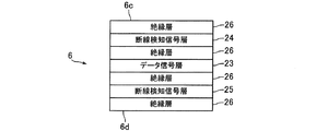
【解決手段】フレキシブルケーブル6は、データ入出力接点に接続されるデータ信号パターン27およびデータ入出力接点以外の接点に接続される信号パターン31が形成されるデータ信号層と、データ信号層の表面および裏面を覆うとともに自身が断線したことを検知するための断線検知信号を伝える断線検知信号パターンが形成される2個の断線検知信号層を備える多層構造に形成され、2個の断線検知信号層の少なくとも一方では、断線検知信号パターンを避けた位置にシールドパターンが形成されている。データ信号パターン27は、2個の断線検知信号層の断線検知信号パターンに覆われるように形成され、信号パターン31は、少なくともその一部が、シールドパターンが形成される断線検知信号層の断線検知信号パターンを避けるように形成されている。
【選択図】図3
Description
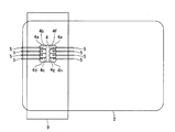
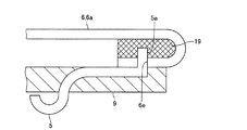
図1は、本発明の実施の形態にかかる媒体処理装置1の概略構成を説明するための側面図である。図2は、図1に示すカード2にIC接点5が接触している状態を示す平面図である。
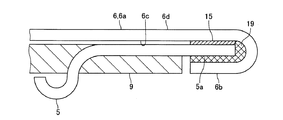
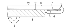
図3は、図1に示すフレキシブルケーブル6の平面図である。図4は、図1に示すIC接点5とフレキシブルケーブル6との接続部の平面図である。図5は、図4のE−E断面の断面図である。図6は、図4のF−F断面の断面図である。図7は、図3のG−G断面の断面図である。図8は、図1に示すフレキシブルケーブル6内の信号パターンの接続関係を示すブロック図である。
以上説明したように、本形態のフレキシブルケーブル6では、データ信号パターン27は、断線検知信号層24の断線検知信号パターン47と、断線検知信号層25の断線検知信号パターン47とに覆われるように形成されている。そのため、犯罪者がデータ信号パターン27へデータ不正取得用の信号線を取り付けようとしたときに、犯罪行為が行われていることを断線検知信号パターン47を用いて検知することが可能になる。また、本形態のフレキシブルケーブル6には、データ信号パターン27が接続されるスルーホールは形成されていない。したがって、本形態では、データ信号パターン27へのデータ不正取得用の信号線の取付を防止することが可能になり、その結果、フレキシブルケーブル6からのデータの不正取得を防止することが可能になる。
上述した形態および変形例は、本発明の好適な形態の一例ではあるが、これに限定されるものではなく本発明の要旨を変更しない範囲において種々変形実施が可能である。
5 IC接点(データ入出力接点、接点)
6 フレキシブルケーブル
6a 接点接続部
6b 折返し部(端子覆部)
17、18 ランド
23 データ信号層
24 断線検知信号層(第1断線検知信号層)
25 断線検知信号層(第2断線検知信号層)
27 データ信号パターン
29 電源パターン(信号パターン)
30 リセット信号パターン(信号パターン)
31 クロック信号パターン(信号パターン)
32 予備パターン(信号パターン)
33 グランドパターン(信号パターン)
34 プログラム電源パターン(信号パターン)
35 予備パターン(信号パターン)
47 断線検知信号パターン
47A 断線検知信号パターン(第1断線検知信号パターン)
47B 断線検知信号パターン(第2断線検知信号パターン)
55 短絡検知信号パターン
R IC接点の配置領域(接点の配置領域)
Claims (11)
- データの入力および/または出力を行うためのデータ入出力接点および前記データ入出力接点以外の複数の接点に接続されるフレキシブルケーブルにおいて、
前記データ入出力接点に接続されるデータ信号パターンおよび複数の前記接点に接続される複数の信号パターンが形成されるデータ信号層と、前記データ信号層の表面を覆うとともに自身が断線したことを検知するための断線検知信号を伝える断線検知信号パターンが形成される第1断線検知信号層と、前記データ信号層の裏面を覆うとともに自身が断線したことを検知するための断線検知信号を伝える断線検知信号パターンが形成される第2断線検知信号層とを備える多層構造に形成され、
前記第1断線検知信号層および/または前記第2断線検知信号層では、前記断線検知信号パターンを避けた位置にシールドパターンが形成され、
前記データ信号パターンは、前記第1断線検知信号層の前記断線検知信号パターンと前記第2断線検知信号層の前記断線検知信号パターンとに覆われるように形成され、
前記信号パターンは、少なくともその一部が、前記シールドパターンが形成される前記第1断線検知信号層および/または前記第2断線検知信号層の前記断線検知信号パターンを避けるように形成されていることを特徴とするフレキシブルケーブル。 - 前記データ信号層には、前記信号パターンとして、クロック信号を伝えるクロック信号パターンが形成され、
前記クロック信号パターンを除く前記信号パターンは、少なくともその一部が、前記シールドパターンに覆われるように形成され、
前記クロック信号パターンは、少なくともその一部が、前記シールドパターンを避けるように形成されていることを特徴とする請求項1記載のフレキシブルケーブル。 - 一方向へ細長い長尺状に形成され、
前記シールドパターンが形成される前記第1断線検知信号層および/または前記第2断線検知信号層の前記断線検知信号パターンは、前記フレキシブルケーブルの幅方向の一端側に形成され、
前記クロック信号パターンは、前記フレキシブルケーブルの幅方向の他端部に形成されていることを特徴とする請求項2記載のフレキシブルケーブル。 - 前記データ入出力接点および複数の前記接点に接続される接点接続部を備え、
前記接点接続部の面積は、前記データ入出力接点および複数の前記接点の配置領域の面積よりも広くなっていることを特徴とする請求項1から3のいずれかに記載のフレキシブルケーブル。 - 前記接点接続部における前記第1断線検知信号層または前記第2断線検知信号層のいずれか一方の全域に前記断線検知信号パターンが形成されていることを特徴とする請求項4記載のフレキシブルケーブル。
- 一方向へ細長い長尺状に形成され、
前記断線検知信号パターンは、前記フレキシブルケーブルの幅方向で複数回折り返されて形成されていることを特徴とする請求項1から5のいずれかに記載のフレキシブルケーブル。 - 前記第1断線検知信号層および前記第2断線検知信号層には、前記断線検知信号パターンとの間の短絡を検知するための短絡検知信号を伝える短絡検知信号パターンが形成されていることを特徴とする請求項1から6のいずれかに記載のフレキシブルケーブル。
- 請求項1から7のいずれかに記載のフレキシブルケーブルと、前記データ入出力接点および複数の前記接点とを備えることを特徴とする媒体処理装置。
- 前記フレキシブルケーブルは、前記データ入出力接点および複数の前記接点に接続される接点接続部と、前記接点接続部に繋がるように形成され少なくとも前記データ入出力接点と前記接点接続部との接続部分を覆うように折り返されて前記接点接続部に固定される端子覆部とを備えることを特徴とする請求項8記載の媒体処理装置。
- 前記第1断線検知信号層および/または前記第2断線検知信号層には、前記断線検知信号の入力側の前記断線検知信号パターンである第1断線検知信号パターンと、前記断線検知信号の出力側の前記断線検知信号パターンである第2断線検知信号パターンとが形成され、
前記接点接続部および前記端子覆部には、前記第1断線検知信号パターンと前記第2断線検知信号パターンとを繋げるためのランドが形成され、
前記端子覆部の前記ランドが前記接点接続部の前記ランドに半田付けされることで、前記端子覆部が前記接点接続部に固定され、
前記端子覆部の前記ランドが前記接点接続部の前記ランドに半田付けされると、前記第1断線検知信号パターンと前記第2断線検知信号パターンとが繋がることを特徴とする請求項9記載の媒体処理装置。 - 前記フレキシブルケーブルが接続されるコネクタを備え、
前記断線検知信号パターンは、前記コネクタからの前記フレキシブルケーブルの抜けを検知する機能を果たしていることを特徴とする請求項8から10のいずれかに記載の媒体処理装置。
Priority Applications (3)
| Application Number | Priority Date | Filing Date | Title |
|---|---|---|---|
| JP2011066520A JP5801073B2 (ja) | 2011-03-24 | 2011-03-24 | フレキシブルケーブルおよび媒体処理装置 |
| US13/876,643 US9053835B2 (en) | 2011-03-24 | 2012-02-15 | Flexible cable and medium processing device |
| PCT/JP2012/053446 WO2012127938A1 (ja) | 2011-03-24 | 2012-02-15 | フレキシブルケーブルおよび媒体処理装置 |
Applications Claiming Priority (1)
| Application Number | Priority Date | Filing Date | Title |
|---|---|---|---|
| JP2011066520A JP5801073B2 (ja) | 2011-03-24 | 2011-03-24 | フレキシブルケーブルおよび媒体処理装置 |
Publications (2)
| Publication Number | Publication Date |
|---|---|
| JP2012204527A true JP2012204527A (ja) | 2012-10-22 |
| JP5801073B2 JP5801073B2 (ja) | 2015-10-28 |
Family
ID=46879102
Family Applications (1)
| Application Number | Title | Priority Date | Filing Date |
|---|---|---|---|
| JP2011066520A Expired - Fee Related JP5801073B2 (ja) | 2011-03-24 | 2011-03-24 | フレキシブルケーブルおよび媒体処理装置 |
Country Status (3)
| Country | Link |
|---|---|
| US (1) | US9053835B2 (ja) |
| JP (1) | JP5801073B2 (ja) |
| WO (1) | WO2012127938A1 (ja) |
Cited By (4)
| Publication number | Priority date | Publication date | Assignee | Title |
|---|---|---|---|---|
| JP2016110414A (ja) * | 2014-12-08 | 2016-06-20 | 日本電産サンキョー株式会社 | カードリーダ |
| US10201078B2 (en) | 2017-03-30 | 2019-02-05 | Nidec Sankyo Corporation | Flexible printed circuit board and card reader |
| JP2020057044A (ja) * | 2018-09-28 | 2020-04-09 | 日本電産サンキョー株式会社 | カードリーダ |
| US10922499B2 (en) | 2017-09-26 | 2021-02-16 | Nidec Sankyo Corporation | Card reader |
Families Citing this family (6)
| Publication number | Priority date | Publication date | Assignee | Title |
|---|---|---|---|---|
| JP5801073B2 (ja) * | 2011-03-24 | 2015-10-28 | 日本電産サンキョー株式会社 | フレキシブルケーブルおよび媒体処理装置 |
| JP5602668B2 (ja) * | 2011-03-24 | 2014-10-08 | 日本電産サンキョー株式会社 | 媒体処理装置およびフレキシブルケーブル |
| FR3008575B1 (fr) * | 2013-07-12 | 2016-12-23 | Cie Ind Et Financiere D'ingenierie Ingenico | Flexible securise |
| CN103558516A (zh) * | 2013-10-25 | 2014-02-05 | 淮南新光神光纤线缆有限公司 | 一种多芯电缆交流耐电压性能试验的方法 |
| JP6276635B2 (ja) * | 2014-04-14 | 2018-02-07 | 日本電産サンキョー株式会社 | プリント基板およびカードリーダ |
| CN106169332A (zh) * | 2016-08-23 | 2016-11-30 | 安徽博达通信工程监理有限责任公司 | 基于液体压力传感传输的多级检测式电缆 |
Citations (3)
| Publication number | Priority date | Publication date | Assignee | Title |
|---|---|---|---|---|
| JP2001036202A (ja) * | 1999-07-15 | 2001-02-09 | Sankyo Seiki Mfg Co Ltd | 回路接続基板及びicカードリーダの回路接続装置 |
| JP2003099908A (ja) * | 2001-09-25 | 2003-04-04 | Sony Corp | 回転磁気ヘッド装置 |
| JP2008293628A (ja) * | 2007-04-27 | 2008-12-04 | Techreco Co Ltd | 磁気ヘッド |
Family Cites Families (5)
| Publication number | Priority date | Publication date | Assignee | Title |
|---|---|---|---|---|
| JPH0366420U (ja) * | 1989-10-31 | 1991-06-27 | ||
| US7699225B2 (en) * | 2007-04-27 | 2010-04-20 | Techreco Company, Ltd. | Magnetic head for reading data |
| US20110062239A1 (en) * | 2009-09-12 | 2011-03-17 | Rachel Lau | Electronic payment card manufacturing process |
| JP5801073B2 (ja) * | 2011-03-24 | 2015-10-28 | 日本電産サンキョー株式会社 | フレキシブルケーブルおよび媒体処理装置 |
| FR2985153B1 (fr) * | 2011-12-23 | 2017-07-28 | Cie Ind Et Financiere D'ingenierie Ingenico | Dispositif de protection d'un circuit imprime electronique. |
-
2011
- 2011-03-24 JP JP2011066520A patent/JP5801073B2/ja not_active Expired - Fee Related
-
2012
- 2012-02-15 WO PCT/JP2012/053446 patent/WO2012127938A1/ja active Application Filing
- 2012-02-15 US US13/876,643 patent/US9053835B2/en not_active Expired - Fee Related
Patent Citations (3)
| Publication number | Priority date | Publication date | Assignee | Title |
|---|---|---|---|---|
| JP2001036202A (ja) * | 1999-07-15 | 2001-02-09 | Sankyo Seiki Mfg Co Ltd | 回路接続基板及びicカードリーダの回路接続装置 |
| JP2003099908A (ja) * | 2001-09-25 | 2003-04-04 | Sony Corp | 回転磁気ヘッド装置 |
| JP2008293628A (ja) * | 2007-04-27 | 2008-12-04 | Techreco Co Ltd | 磁気ヘッド |
Cited By (5)
| Publication number | Priority date | Publication date | Assignee | Title |
|---|---|---|---|---|
| JP2016110414A (ja) * | 2014-12-08 | 2016-06-20 | 日本電産サンキョー株式会社 | カードリーダ |
| US10201078B2 (en) | 2017-03-30 | 2019-02-05 | Nidec Sankyo Corporation | Flexible printed circuit board and card reader |
| US10922499B2 (en) | 2017-09-26 | 2021-02-16 | Nidec Sankyo Corporation | Card reader |
| JP2020057044A (ja) * | 2018-09-28 | 2020-04-09 | 日本電産サンキョー株式会社 | カードリーダ |
| JP7137423B2 (ja) | 2018-09-28 | 2022-09-14 | 日本電産サンキョー株式会社 | カードリーダ |
Also Published As
| Publication number | Publication date |
|---|---|
| US9053835B2 (en) | 2015-06-09 |
| WO2012127938A1 (ja) | 2012-09-27 |
| US20140009878A1 (en) | 2014-01-09 |
| JP5801073B2 (ja) | 2015-10-28 |
Similar Documents
| Publication | Publication Date | Title |
|---|---|---|
| JP5801073B2 (ja) | フレキシブルケーブルおよび媒体処理装置 | |
| US7699225B2 (en) | Magnetic head for reading data | |
| JP4342582B2 (ja) | 磁気ヘッド | |
| JP5781725B2 (ja) | 磁気ヘッドおよびこの磁気ヘッドを備えるカードリーダ | |
| JP5690226B2 (ja) | カードリーダ | |
| CA2622771A1 (en) | Protection against manipulation and through-drilling for an apparatus to be connected to an electrical circuit | |
| JP5602668B2 (ja) | 媒体処理装置およびフレキシブルケーブル | |
| US10201078B2 (en) | Flexible printed circuit board and card reader | |
| US20150340124A1 (en) | Printed circuit board and card reader | |
| US10360413B2 (en) | Printed circuit board and card reader | |
| JP2023106070A (ja) | プリント基板 | |
| JP6446338B2 (ja) | カードリーダ | |
| CN101673553B (zh) | 磁头 | |
| JP6840010B2 (ja) | カードリーダ | |
| JP7137423B2 (ja) | カードリーダ | |
| JP2019149214A (ja) | 磁気ヘッドユニットおよびカードリーダ | |
| US11950359B2 (en) | Card reader | |
| US9396371B2 (en) | Non-contact type information processing device | |
| CN101320568A (zh) | 磁头 |
Legal Events
| Date | Code | Title | Description |
|---|---|---|---|
| A621 | Written request for application examination |
Free format text: JAPANESE INTERMEDIATE CODE: A621 Effective date: 20140205 |
|
| A131 | Notification of reasons for refusal |
Free format text: JAPANESE INTERMEDIATE CODE: A131 Effective date: 20150227 |
|
| TRDD | Decision of grant or rejection written | ||
| A01 | Written decision to grant a patent or to grant a registration (utility model) |
Free format text: JAPANESE INTERMEDIATE CODE: A01 Effective date: 20150819 |
|
| A61 | First payment of annual fees (during grant procedure) |
Free format text: JAPANESE INTERMEDIATE CODE: A61 Effective date: 20150826 |
|
| R150 | Certificate of patent or registration of utility model |
Ref document number: 5801073 Country of ref document: JP Free format text: JAPANESE INTERMEDIATE CODE: R150 |
|
| LAPS | Cancellation because of no payment of annual fees |