WO2012124464A1 - Cellule solaire - Google Patents
Cellule solaire Download PDFInfo
- Publication number
- WO2012124464A1 WO2012124464A1 PCT/JP2012/054891 JP2012054891W WO2012124464A1 WO 2012124464 A1 WO2012124464 A1 WO 2012124464A1 JP 2012054891 W JP2012054891 W JP 2012054891W WO 2012124464 A1 WO2012124464 A1 WO 2012124464A1
- Authority
- WO
- WIPO (PCT)
- Prior art keywords
- solar cell
- electrode
- back surface
- metal film
- connection
- Prior art date
Links
- 229910052751 metal Inorganic materials 0.000 claims abstract description 67
- 239000002184 metal Substances 0.000 claims abstract description 67
- 238000006243 chemical reaction Methods 0.000 claims abstract description 32
- 239000000463 material Substances 0.000 claims description 13
- 239000011347 resin Substances 0.000 claims description 6
- 229920005989 resin Polymers 0.000 claims description 6
- 238000000034 method Methods 0.000 description 18
- 230000035882 stress Effects 0.000 description 11
- 239000004065 semiconductor Substances 0.000 description 8
- 239000000758 substrate Substances 0.000 description 8
- 229910045601 alloy Inorganic materials 0.000 description 7
- 239000000956 alloy Substances 0.000 description 7
- 239000000470 constituent Substances 0.000 description 5
- 230000000694 effects Effects 0.000 description 4
- 150000002739 metals Chemical class 0.000 description 4
- PXHVJJICTQNCMI-UHFFFAOYSA-N Nickel Chemical compound [Ni] PXHVJJICTQNCMI-UHFFFAOYSA-N 0.000 description 3
- 239000000969 carrier Substances 0.000 description 3
- 229910052802 copper Inorganic materials 0.000 description 3
- 239000010949 copper Substances 0.000 description 3
- 239000011159 matrix material Substances 0.000 description 3
- 230000001681 protective effect Effects 0.000 description 3
- 238000007650 screen-printing Methods 0.000 description 3
- 229910052709 silver Inorganic materials 0.000 description 3
- 238000004544 sputter deposition Methods 0.000 description 3
- 238000007740 vapor deposition Methods 0.000 description 3
- XLOMVQKBTHCTTD-UHFFFAOYSA-N Zinc monoxide Chemical compound [Zn]=O XLOMVQKBTHCTTD-UHFFFAOYSA-N 0.000 description 2
- 239000000853 adhesive Substances 0.000 description 2
- 230000001070 adhesive effect Effects 0.000 description 2
- 229910052782 aluminium Inorganic materials 0.000 description 2
- 230000015572 biosynthetic process Effects 0.000 description 2
- 229910052804 chromium Inorganic materials 0.000 description 2
- 239000011651 chromium Substances 0.000 description 2
- 238000009792 diffusion process Methods 0.000 description 2
- 239000002019 doping agent Substances 0.000 description 2
- 238000005530 etching Methods 0.000 description 2
- 229910021421 monocrystalline silicon Inorganic materials 0.000 description 2
- 229910052759 nickel Inorganic materials 0.000 description 2
- 238000007645 offset printing Methods 0.000 description 2
- 238000007747 plating Methods 0.000 description 2
- 229910052719 titanium Inorganic materials 0.000 description 2
- 239000010936 titanium Substances 0.000 description 2
- 239000004925 Acrylic resin Substances 0.000 description 1
- 229920000178 Acrylic resin Polymers 0.000 description 1
- VYZAMTAEIAYCRO-UHFFFAOYSA-N Chromium Chemical compound [Cr] VYZAMTAEIAYCRO-UHFFFAOYSA-N 0.000 description 1
- RYGMFSIKBFXOCR-UHFFFAOYSA-N Copper Chemical compound [Cu] RYGMFSIKBFXOCR-UHFFFAOYSA-N 0.000 description 1
- BQCADISMDOOEFD-UHFFFAOYSA-N Silver Chemical compound [Ag] BQCADISMDOOEFD-UHFFFAOYSA-N 0.000 description 1
- RTAQQCXQSZGOHL-UHFFFAOYSA-N Titanium Chemical compound [Ti] RTAQQCXQSZGOHL-UHFFFAOYSA-N 0.000 description 1
- 239000002253 acid Substances 0.000 description 1
- XAGFODPZIPBFFR-UHFFFAOYSA-N aluminium Chemical compound [Al] XAGFODPZIPBFFR-UHFFFAOYSA-N 0.000 description 1
- 238000005336 cracking Methods 0.000 description 1
- 238000001312 dry etching Methods 0.000 description 1
- 239000003822 epoxy resin Substances 0.000 description 1
- 230000006355 external stress Effects 0.000 description 1
- 239000000945 filler Substances 0.000 description 1
- 229910003437 indium oxide Inorganic materials 0.000 description 1
- PJXISJQVUVHSOJ-UHFFFAOYSA-N indium(iii) oxide Chemical compound [O-2].[O-2].[O-2].[In+3].[In+3] PJXISJQVUVHSOJ-UHFFFAOYSA-N 0.000 description 1
- 230000031700 light absorption Effects 0.000 description 1
- 238000004519 manufacturing process Methods 0.000 description 1
- 230000003287 optical effect Effects 0.000 description 1
- 238000001579 optical reflectometry Methods 0.000 description 1
- 239000012466 permeate Substances 0.000 description 1
- 229910021420 polycrystalline silicon Inorganic materials 0.000 description 1
- 229920000647 polyepoxide Polymers 0.000 description 1
- 238000010248 power generation Methods 0.000 description 1
- 238000007789 sealing Methods 0.000 description 1
- 239000004332 silver Substances 0.000 description 1
- 229910000679 solder Inorganic materials 0.000 description 1
- 229920002803 thermoplastic polyurethane Polymers 0.000 description 1
- 229910052718 tin Inorganic materials 0.000 description 1
- 239000011135 tin Substances 0.000 description 1
- 238000001039 wet etching Methods 0.000 description 1
- 229910052725 zinc Inorganic materials 0.000 description 1
- 239000011701 zinc Substances 0.000 description 1
- 239000011787 zinc oxide Substances 0.000 description 1
Images


Classifications
-
- H—ELECTRICITY
- H01—ELECTRIC ELEMENTS
- H01L—SEMICONDUCTOR DEVICES NOT COVERED BY CLASS H10
- H01L31/00—Semiconductor devices sensitive to infrared radiation, light, electromagnetic radiation of shorter wavelength or corpuscular radiation and specially adapted either for the conversion of the energy of such radiation into electrical energy or for the control of electrical energy by such radiation; Processes or apparatus specially adapted for the manufacture or treatment thereof or of parts thereof; Details thereof
- H01L31/02—Details
- H01L31/0224—Electrodes
- H01L31/022408—Electrodes for devices characterised by at least one potential jump barrier or surface barrier
- H01L31/022425—Electrodes for devices characterised by at least one potential jump barrier or surface barrier for solar cells
- H01L31/022433—Particular geometry of the grid contacts
-
- Y—GENERAL TAGGING OF NEW TECHNOLOGICAL DEVELOPMENTS; GENERAL TAGGING OF CROSS-SECTIONAL TECHNOLOGIES SPANNING OVER SEVERAL SECTIONS OF THE IPC; TECHNICAL SUBJECTS COVERED BY FORMER USPC CROSS-REFERENCE ART COLLECTIONS [XRACs] AND DIGESTS
- Y02—TECHNOLOGIES OR APPLICATIONS FOR MITIGATION OR ADAPTATION AGAINST CLIMATE CHANGE
- Y02E—REDUCTION OF GREENHOUSE GAS [GHG] EMISSIONS, RELATED TO ENERGY GENERATION, TRANSMISSION OR DISTRIBUTION
- Y02E10/00—Energy generation through renewable energy sources
- Y02E10/50—Photovoltaic [PV] energy
Definitions
- the present invention relates to a solar cell.
- Patent Document 1 describes a solar cell including a photoelectric conversion unit, a light receiving surface electrode disposed on a light receiving surface of the photoelectric conversion unit, and a back electrode disposed on a back surface.
- each of the light-receiving surface electrode and the back surface electrode includes a plurality of finger portions and a bus bar portion electrically connected to the plurality of finger portions.
- the present invention has been made in view of such a point, and an object thereof is to provide a solar cell having improved photoelectric conversion efficiency.
- the solar cell according to the present invention includes a photoelectric conversion unit, a light receiving surface electrode, and a back electrode.
- the photoelectric conversion unit has a light receiving surface and a back surface.
- the light receiving surface electrode is disposed on the light receiving surface.
- the light-receiving surface electrode contains a metal.
- the back electrode is arranged on the back surface.
- the back electrode includes a metal.
- the back electrode includes a metal film and a plurality of connection electrodes.
- the metal film is disposed on at least a part of the back surface.
- the plurality of connection electrodes are arranged on the metal film.
- the plurality of connection electrodes are arranged at intervals from one another along one direction.
- the solar cell according to the present invention further includes a first convex portion.
- the 1st convex part is located between the connection electrodes adjacent in one direction.
- a solar cell having improved photoelectric conversion efficiency can be provided.
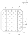
- FIG. 1 is a schematic plan view of a light receiving surface of the solar cell according to the first embodiment.
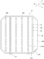
- FIG. 2 is a schematic plan view of the back surface of the solar cell according to the first embodiment.
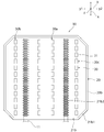
- FIG. 3 is a schematic plan view of the back surface of the solar cell according to the second embodiment.
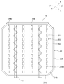
- FIG. 4 is a schematic plan view of the back surface of the solar cell according to the third embodiment.
- FIG. 5 is a schematic plan view of the back surface of the solar cell according to the fourth embodiment.
- FIG. 6 is a schematic plan view of the back surface of the solar cell according to the fifth embodiment.
- FIG. 7 is a schematic plan view of the back surface of the solar cell according to the sixth embodiment.
- FIG. 8 is a schematic plan view of the back surface of the solar cell according to the seventh embodiment.
- FIG. 1 is a schematic plan view of a light receiving surface of the solar cell according to the first embodiment.
- FIG. 2 is a schematic plan view of the back surface of the solar cell according to the first embodiment.
- FIG. 9 is a schematic plan view of the back surface of the solar cell according to the eighth embodiment.
- FIG. 10 is a schematic plan view of the back surface of the solar cell according to the ninth embodiment.
- FIG. 11 is a schematic plan view of the back surface of the solar cell according to the tenth embodiment.
- FIG. 12 is a schematic plan view of the back surface of the solar cell according to the eleventh embodiment.
- FIG. 1 is a schematic plan view of a light receiving surface of the solar cell according to the first embodiment.
- FIG. 2 is a schematic plan view of the back surface of the solar cell according to the first embodiment.
- the solar cell 10 has a photoelectric conversion unit 20.
- the photoelectric conversion unit 20 is a member that generates carriers such as electrons and holes by receiving light.
- the photoelectric conversion unit 20 is, for example, a substrate made of a crystalline semiconductor having one conductivity type, and a first amorphous semiconductor layer having another conductivity type disposed on one main surface of the substrate. And a second amorphous semiconductor layer having one conductivity type disposed on the other main surface of the substrate.
- an i-type amorphous semiconductor layer having a thickness that does not substantially contribute to power generation may be provided between at least one of the first and second amorphous semiconductor layers and the crystalline semiconductor substrate.
- the photoelectric conversion unit 20 may have a substrate in which an n-type dopant diffusion region and a p-type dopant diffusion region are exposed on the surface.
- the photoelectric conversion unit 20 has a light receiving surface 20a and a back surface 20b.
- Each of the light receiving surface 20a and the back surface 20b has a texture structure.
- the “texture structure” refers to a concavo-convex structure formed to suppress surface reflection and increase the light absorption amount of the photoelectric conversion unit.
- Specific examples of the texture structure include a pyramidal (quadrangular pyramid or quadrangular frustum-shaped) uneven structure obtained by performing anisotropic etching on the surface of a single crystal silicon substrate having a (100) plane. .
- texture structure is not limited to this, and isotropic etching such as wet etching using acid or dry etching is performed on the surface of a substrate made of a crystalline semiconductor such as single crystal silicon or polycrystalline silicon.
- isotropic etching such as wet etching using acid or dry etching is performed on the surface of a substrate made of a crystalline semiconductor such as single crystal silicon or polycrystalline silicon.
- the resulting uneven structure may be used.
- the light-receiving surface electrode 21a has a plurality of finger portions 21a1 and a plurality of bus bar portions 21a2.
- Each of the plurality of finger portions 21a1 has a line shape extending along the y direction.
- the plurality of finger portions 21a1 are arranged at predetermined intervals along the x direction.
- Each of the plurality of bus bar portions 21a2 extends along the x direction orthogonal to the y direction.
- Each of the plurality of bus bar portions 21a2 is electrically connected to the plurality of finger portions 21a1.
- the plurality of finger portions 21a1 collects carriers generated by the photoelectric conversion unit 20 by light reception.
- the bus bar portion 21a2 collects the carriers collected by the plurality of finger portions 21a1.
- the constituent material of the light receiving surface electrode 21a includes a metal.
- the light-receiving surface electrode 21a can be made of, for example, a metal such as silver, copper, aluminum, titanium, nickel, or chromium, or an alloy containing one or more of these metals.
- the light-receiving surface electrode 21a may be configured by a laminated body of a plurality of conductive layers made of the above metal or alloy, for example.
- the formation method of the light-receiving surface electrode 21a is not particularly limited.
- the light-receiving surface electrode 21a can be formed using a conductive paste such as an Ag paste, for example.
- the light receiving surface electrode 21a can be formed by using, for example, a sputtering method, a vapor deposition method, a screen printing method, a plating method, or the like.
- the back electrode 21b includes a metal film 21b1 and a plurality of connection electrodes 21b2.
- the back electrode 21b has a larger area than the light receiving surface electrode 21a. For this reason, the photoelectric conversion unit 20 can receive a lot of light.
- the “metal film” includes an alloy film.
- the metal film 21b1 is disposed on at least a part of the back surface 20b. Specifically, in the present embodiment, the metal film 21b1 is disposed on the inner region excluding the edge portion of the back surface 20b. The metal film 21b1 may be provided on the entire back surface 20b.
- the metal film 21b1 has such a thickness that unevenness having a shape corresponding to the texture structure exists on the surface opposite to the back surface 20b of the metal film 21b1.
- the thickness of the metal film 21b1 is preferably about 0.1 ⁇ m to 5 ⁇ m, for example.
- the constituent material of the metal film 21b1 is not particularly limited, but it is preferable that the metal film 21b1 has high light reflectivity and high conductivity.
- the metal film 21b1 can be made of a metal such as Ag, Al, Cu, Ni, Cr, Ti, Sn, Zn, or an alloy containing one or more of these metals.
- the metal film 21b1 may be configured by a laminated body of a plurality of films made of the above metals or alloys.
- the metal film 21b1 is disposed on the back surface 20b, and is disposed on the first Ag film having a thickness of about 0.1 ⁇ m to 1 ⁇ m and the first Ag film. It can be constituted by a laminate of an Al film having a thickness of about 0.1 ⁇ m to 1 ⁇ m and a second Ag film disposed on the Al film and having a thickness of about 0.1 ⁇ m to 1 ⁇ m.
- the formation method of the metal film 21b1 is not particularly limited.
- the metal film 21b1 can be formed using a conductive paste such as an Ag paste, for example.
- the metal film 21b1 can be formed using, for example, a sputtering method, a vapor deposition method, a screen printing method, an offset printing method, an ink jet method, a plating method, or the like.
- the metal film 21b1 may be formed directly on the back surface 20b, but a translucent conductive film may be provided between the metal film 21b1 and the back surface 20b. By providing the translucent conductive film, the adhesion to the back surface 20b of the metal film 21b1 can be improved.
- the translucent conductive film can be made of a translucent conductive oxide such as indium oxide or zinc oxide. The thickness of the translucent conductive film is preferably about 0.05 ⁇ m to 3 ⁇ m.
- connection electrodes 21b2 for electrical connection are disposed on the metal film 21b1.
- the plurality of connection electrodes 21b2 are arranged at intervals from each other along one direction (y direction).
- Each of the plurality of connection electrodes 21b2 is provided in a straight line extending in another direction (x direction) perpendicular to one direction (y direction).
- the number of connection electrodes 21b2 is preferably the same as the number of bus bar portions 21a2. Further, the connection electrode 21b2 is preferably provided in a positional relationship overlapping the bus bar portion 21a2. By doing in this way, the connection of the wiring material mentioned later becomes easy.
- the connection electrode 21b2 is an electrode that is electrically connected to the wiring member 11 when the solar cell module is configured by electrically connecting the plurality of solar cells 10 with the wiring member 11, for example. That is, by electrically connecting mainly the bus bar portion 21a2 of the light receiving surface electrode 21a of one solar cell 10 and the connection electrode 21b2 of the back surface electrode 21b of the other solar cell 10 by the wiring member 11, A solar cell string in which a plurality of solar cells 10 are electrically connected is configured.
- the solar cell string is configured by sealing the solar cell string with a protective member on the light receiving surface side, a protective member on the back surface side, and a filler layer filled between the protective members.
- the wiring material 11 and the solar cell 10 can be connected using solder or a resin adhesive.
- the connecting electrode 21b2 has a thickness protruding from the convex portion of the texture structure of the back surface 20b.
- the connection electrode 21b2 is preferably thicker than the metal film 21b1. Specifically, the thickness of the connection electrode 21b2 is preferably in the range of 5 ⁇ m to 30 ⁇ m.
- connection electrode 21b2 includes a metal.
- the connection electrode 21b2 can be made of, for example, a metal such as Cu, Ag, or Sn, or an alloy containing at least one of these metals. Further, the connection electrode 21b2 may be configured by a laminated body of a plurality of films made of the above metal or alloy.
- connection electrode 21b2 can be formed using, for example, a conductive paste such as an Ag paste.
- the connection electrode 21b2 can be formed using, for example, a sputtering method, a vapor deposition method, a screen printing method, a dispensing method, an offset printing method, an ink jet method, or the like.
- a plurality of convex portions 30 are arranged on the metal film 21b1.
- the plurality of convex portions 30 include a first convex portion 30a, a second convex portion 30b, and a third convex portion 30c.
- the first protrusion 30a is located between adjacent connection electrodes 21b2 in one direction (y direction).
- the 2nd convex part 30b is located in the one side (y1 side) in one direction (y direction) of the field in which a plurality of connection electrodes 21b2 were provided.
- the 3rd convex part 30c is located in the other side (y2 side) in one direction (y direction) of the field in which a plurality of connection electrodes 21b2 were provided.
- Each of the plurality of protrusions 30 includes a plurality of protrusions 31 arranged in a straight line at intervals in the x direction.
- the height of the convex portion 30 is preferably substantially the same as or higher than the height of the connection electrode 21b2.
- the width along the y direction of the convex portion 30 is preferably 1 to 10 times the width along the y direction of the connection electrode 21b2.
- the constituent material of the convex part 30 is not particularly limited.
- Specific examples of the convex portion 30 include, for example, resin and the same material as the connection electrode 21b2. By forming the convex part 30 with the same material as the connection electrode 21b2, the convex part 30 and the connection electrode 21b2 can be formed in the same process. Therefore, manufacture of the solar cell 10 becomes easy.
- Specific examples of the resin that is preferably used as the constituent material of the convex portion 30 include, for example, an epoxy resin, an acrylic resin, and a urethane resin.
- the metal film 21b1 is disposed.
- the metal film 21b1 covers at least a part of the back surface 20b. For this reason, the light which permeate
- the metal film 21b1 has such a thickness that unevenness having a shape corresponding to the texture structure exists on the surface opposite to the back surface 20b of the metal film 21b1. Therefore, the optical path length in the photoelectric conversion unit 20 of the light reflected by the metal film 21b1 can be increased. Therefore, more improved photoelectric conversion efficiency can be obtained.
- the thickness of the semiconductor substrate used for the photoelectric conversion unit 20 can be reduced to, for example, 180 ⁇ m or less.
- the thickness of the metal film 21b1 is preferably 0.1 ⁇ m or more. From the viewpoint of obtaining higher reliability, the thickness of the metal film 21b1 is preferably 5 ⁇ m or less.
- the connection electrode 21b2 is preferably thicker than the metal film 21b1. Specifically, the thickness of the connection electrode 21b2 is preferably 5 ⁇ m or more. However, if the thickness of the connection electrode 21b2 is too thick, the connection electrode 21b2 is easily peeled from the metal film 21b1 due to the stress of the connection electrode 21b2. Therefore, the thickness of the connection electrode 21b2 is preferably 20 ⁇ m or less.
- connection electrode 21b2 has a thickness protruding from the convex portion of the texture structure of the back surface 20b.
- connection electrode 21b2 extends from the one side end side in the x direction of the back surface 20b to the other side end side.
- the connection electrode 21b2 has a length of about 70% or more of the length of the photoelectric conversion unit 20. For this reason, even when a stress is generated between the wiring member 11 and the connection electrode 21b2 due to a temperature change or the like, the stress per unit area can be reduced. Therefore, peeling of the wiring material 11 can be suppressed more effectively.
- the back surface 20b has a texture structure. For this reason, light is scattered on the back surface 20b, and the light is easily confined in the photoelectric conversion unit 20, so that more improved photoelectric conversion efficiency can be obtained.
- the metal film 21b1 has such a thickness that unevenness having a shape corresponding to the texture structure exists on the surface opposite to the back surface 20b of the metal film 21b1. For this reason, the adhesion strength between the metal film 21b1 and the connection electrode 21b2 can be increased.
- connection electrode 21b2 protrudes from the back surface 20b. For this reason, for example, when the solar cell 10 is in contact with another member during the process after the electrode forming step of the solar cell 10 or during the conveyance, a large stress may be concentrated on the connection electrode 21b2. . As a result, damage such as peeling may occur in a part of the connection electrode 21b2.
- connection electrode 21b2 In contrast, in the solar cell 10, a plurality of convex portions 30 including the first convex portions 30a located between the adjacent connection electrodes 21b2 are provided. For this reason, even when the solar cell 10 comes into contact with another member during the transportation of the solar cell 10, stress is distributed and applied to the connection electrode 21 b 2 and the convex portion 30. Therefore, it is possible to suppress a large stress from being concentrated on the connection electrode 21b2. Therefore, damage to the connection electrode 21b2 can be suppressed.
- the second and third electrodes are provided on both sides of the region where the plurality of connection electrodes 21b2 are provided. Protrusions 30b and 30c are provided. For this reason, it can suppress more effectively that a big stress is intensively added to the electrode 21b2 for a connection. Therefore, damage to the connection electrode 21b2 can be more effectively suppressed.
- the convex portion 30 is arranged between the adjacent connection electrodes 21b2, when the external stress in the direction from the light receiving surface 20a to the back surface 20b is generated between the adjacent connection electrodes 21b2, the convex portion 30 is photoelectric. It works as a support for the conversion unit 20 and can suppress damage such as cracking of the solar cell 10.
- the convex part 30 is resin, the elasticity of the convex part 30 becomes high. For this reason, it can suppress more effectively that big stress is intensively applied to the electrode 21b2 for connection, and can also suppress effectively that stress is applied to the photoelectric conversion part 20 via the convex part 30. FIG. Therefore, damage to the solar cell 10 can be suppressed more effectively.
- the convex part 30 is lower than the connection electrode 21b2, an effect that it is possible to suppress a large stress from being concentrated on the connection electrode 21b2 described above can be obtained, but the effect is further enhanced.
- the height of the convex portion 30 is preferably equal to or higher than the height of the connection electrode 21b2.
- FIG. 3 is a schematic plan view of the back surface of the solar cell according to the second embodiment.
- FIG. 4 is a schematic plan view of the back surface of the solar cell according to the third embodiment.
- FIG. 5 is a schematic plan view of the back surface of the solar cell according to the fourth embodiment.
- FIG. 6 is a schematic plan view of the back surface of the solar cell according to the fifth embodiment.
- FIG. 7 is a schematic plan view of the back surface of the solar cell according to the sixth embodiment.
- each of the plurality of protrusions 30 is configured by a plurality of protrusions 31 arranged at intervals along the x direction.
- the shape of the convex portion 30 is not particularly limited.
- the arrangement of the plurality of convex portions 30 is not particularly limited.
- each of the plurality of convex portions 30 may be a linear convex portion extending along another direction (x direction) perpendicular to one direction (y direction).
- the plurality of convex portions 30 may be configured by a plurality of linear convex portions that are arranged along the x direction and extend along the y direction.
- the convex part 30 is dot-shaped, and the plurality of convex parts 30 may be arranged in a square matrix. Moreover, as shown in FIG. 6, the convex part 30 is dot shape, and the some convex part 30 may be distribute
- the convex part 30 may be zigzag-shaped.
- FIG. 8 is a schematic plan view of the back surface of the solar cell according to the seventh embodiment.
- FIG. 9 is a schematic plan view of the back surface of the solar cell according to the eighth embodiment.
- FIG. 10 is a schematic plan view of the back surface of the solar cell according to the ninth embodiment.
- FIG. 11 is a schematic plan view of the back surface of the solar cell according to the tenth embodiment.
- FIG. 12 is a schematic plan view of the back surface of the solar cell according to the eleventh embodiment.
- connection electrode 21b2 is a linear electrode extending in the x direction.
- shape of the connection electrode is not particularly limited.
- connection electrodes 21b2 may be configured by a plurality of linear electrodes arranged along the x direction and extending along the y direction.
- connection electrodes 21 b 2 are arranged along the x direction, and each crosses the first linear electrode portion extending along the y direction and the first linear electrode portion. And a plurality of electrodes including a plurality of second linear electrode portions extending along the x direction.
- connection electrode 21b2 may be composed of a plurality of V-shaped electrodes arranged along the x direction.
- connection electrode 21b2 may be composed of a plurality of linear electrodes arranged in a matrix.
- connection electrode 21b2 may be formed of a zigzag electrode.
- the convex portion 30 may be the convex portion described in the second to sixth embodiments.
- the light-receiving surface electrode may be a so-called bus bar-less electrode that includes only a plurality of finger portions and does not have a bus bar portion.
- only one connection electrode may be provided, or three or more connection electrodes may be provided along the y direction.
- the shapes of the first to third convex portions may be different from each other.
Abstract
L'invention porte sur une cellule solaire ayant une efficacité de conversion photoélectrique améliorée. Une cellule solaire (10) comprend une unité de conversion photoélectrique (20), une électrode de surface de réception de lumière (21a) qui est agencée sur une surface de réception de lumière (20a) et contient un métal, et une électrode de surface arrière (21b) qui est agencée sur une surface arrière (20b) et contient un métal. L'électrode de surface arrière (21b) comprend un film métallique (21b1) et de multiples électrodes de connexion (21b2). Le film métallique (21b1) est agencé sur au moins une partie de la surface arrière (20b). Les multiples électrodes de connexion (21b2) sont agencées sur le film métallique (21b1). Les multiples électrodes de connexion (21b2) sont disposées selon une direction (y). La cellule solaire (10) comprend en outre une première partie en saillie (30a). La première partie en saillie (30a) est située entre deux quelconques des électrodes de connexion (21b2) qui sont adjacentes l'une à l'autre dans la direction (y).
Applications Claiming Priority (2)
| Application Number | Priority Date | Filing Date | Title |
|---|---|---|---|
| JP2011058175 | 2011-03-16 | ||
| JP2011-058175 | 2011-03-16 |
Publications (1)
| Publication Number | Publication Date |
|---|---|
| WO2012124464A1 true WO2012124464A1 (fr) | 2012-09-20 |
Family
ID=46830540
Family Applications (1)
| Application Number | Title | Priority Date | Filing Date |
|---|---|---|---|
| PCT/JP2012/054891 WO2012124464A1 (fr) | 2011-03-16 | 2012-02-28 | Cellule solaire |
Country Status (1)
| Country | Link |
|---|---|
| WO (1) | WO2012124464A1 (fr) |
Cited By (2)
| Publication number | Priority date | Publication date | Assignee | Title |
|---|---|---|---|---|
| JP2016152411A (ja) * | 2015-02-16 | 2016-08-22 | バオディン イトン ピーヴイ サイエンス アンド テクノロジー カンパニー リミテッド | 光起電力モジュール及びその製造方法 |
| WO2021149438A1 (fr) * | 2020-01-23 | 2021-07-29 | 株式会社カネカ | Cellule solaire et procédé de fabrication de cellule solaire |
Citations (6)
| Publication number | Priority date | Publication date | Assignee | Title |
|---|---|---|---|---|
| JPS61108178A (ja) * | 1984-11-01 | 1986-05-26 | Nec Corp | 太陽電池モジユ−ル |
| JP2002217435A (ja) * | 2001-01-22 | 2002-08-02 | Sharp Corp | 太陽電池セルおよびその製造方法 |
| JP2003069055A (ja) * | 2001-06-13 | 2003-03-07 | Sharp Corp | 太陽電池セルとその製造方法 |
| JP2004119687A (ja) * | 2002-09-26 | 2004-04-15 | Kyocera Corp | 太陽電池素子および太陽電池モジュール |
| JP2007214372A (ja) * | 2006-02-09 | 2007-08-23 | Sharp Corp | 太陽電池およびその製造方法 |
| JP2009164509A (ja) * | 2008-01-10 | 2009-07-23 | Mitsubishi Electric Corp | 太陽電池素子及びその製造方法 |
-
2012
- 2012-02-28 WO PCT/JP2012/054891 patent/WO2012124464A1/fr active Application Filing
Patent Citations (6)
| Publication number | Priority date | Publication date | Assignee | Title |
|---|---|---|---|---|
| JPS61108178A (ja) * | 1984-11-01 | 1986-05-26 | Nec Corp | 太陽電池モジユ−ル |
| JP2002217435A (ja) * | 2001-01-22 | 2002-08-02 | Sharp Corp | 太陽電池セルおよびその製造方法 |
| JP2003069055A (ja) * | 2001-06-13 | 2003-03-07 | Sharp Corp | 太陽電池セルとその製造方法 |
| JP2004119687A (ja) * | 2002-09-26 | 2004-04-15 | Kyocera Corp | 太陽電池素子および太陽電池モジュール |
| JP2007214372A (ja) * | 2006-02-09 | 2007-08-23 | Sharp Corp | 太陽電池およびその製造方法 |
| JP2009164509A (ja) * | 2008-01-10 | 2009-07-23 | Mitsubishi Electric Corp | 太陽電池素子及びその製造方法 |
Cited By (2)
| Publication number | Priority date | Publication date | Assignee | Title |
|---|---|---|---|---|
| JP2016152411A (ja) * | 2015-02-16 | 2016-08-22 | バオディン イトン ピーヴイ サイエンス アンド テクノロジー カンパニー リミテッド | 光起電力モジュール及びその製造方法 |
| WO2021149438A1 (fr) * | 2020-01-23 | 2021-07-29 | 株式会社カネカ | Cellule solaire et procédé de fabrication de cellule solaire |
Similar Documents
| Publication | Publication Date | Title |
|---|---|---|
| JP5687506B2 (ja) | 太陽電池及び太陽電池モジュール | |
| JP5874011B2 (ja) | 太陽電池及び太陽電池モジュール | |
| JP5879538B2 (ja) | 光電変換装置及びその製造方法 | |
| JP5705968B2 (ja) | 光電変換装置及びその製造方法 | |
| JP5445419B2 (ja) | 太陽電池モジュール及びその製造方法 | |
| JP6065009B2 (ja) | 太陽電池モジュール | |
| JP5879512B2 (ja) | 太陽電池モジュール | |
| JP5884077B2 (ja) | 太陽電池及び太陽電池モジュール | |
| JP5273728B2 (ja) | 配線シート付き太陽電池セルおよび太陽電池モジュール | |
| JP7146805B2 (ja) | 太陽電池およびその太陽電池を備えた電子機器 | |
| WO2012124464A1 (fr) | Cellule solaire | |
| US9627557B2 (en) | Solar cell | |
| JP6249368B2 (ja) | 太陽電池モジュール及び太陽電池モジュールの製造方法 | |
| US20150075609A1 (en) | Solar cell, solar cell module | |
| JP5906422B2 (ja) | 太陽電池及び太陽電池モジュール | |
| JP6418558B2 (ja) | 太陽電池 | |
| US20170092797A1 (en) | Solar cell module | |
| JP6191925B2 (ja) | 太陽電池モジュール | |
| JP6681607B2 (ja) | 太陽電池セルおよび太陽電池セルの製造方法 |
Legal Events
| Date | Code | Title | Description |
|---|---|---|---|
| 121 | Ep: the epo has been informed by wipo that ep was designated in this application |
Ref document number: 12758009 Country of ref document: EP Kind code of ref document: A1 |
|
| NENP | Non-entry into the national phase |
Ref country code: DE |
|
| 122 | Ep: pct application non-entry in european phase |
Ref document number: 12758009 Country of ref document: EP Kind code of ref document: A1 |
|
| NENP | Non-entry into the national phase |
Ref country code: JP |