WO2012124464A1 - Solar cell - Google Patents
Solar cell Download PDFInfo
- Publication number
- WO2012124464A1 WO2012124464A1 PCT/JP2012/054891 JP2012054891W WO2012124464A1 WO 2012124464 A1 WO2012124464 A1 WO 2012124464A1 JP 2012054891 W JP2012054891 W JP 2012054891W WO 2012124464 A1 WO2012124464 A1 WO 2012124464A1
- Authority
- WO
- WIPO (PCT)
- Prior art keywords
- solar cell
- electrode
- back surface
- metal film
- connection
- Prior art date
Links
- 229910052751 metal Inorganic materials 0.000 claims abstract description 67
- 239000002184 metal Substances 0.000 claims abstract description 67
- 238000006243 chemical reaction Methods 0.000 claims abstract description 32
- 239000000463 material Substances 0.000 claims description 13
- 239000011347 resin Substances 0.000 claims description 6
- 229920005989 resin Polymers 0.000 claims description 6
- 238000000034 method Methods 0.000 description 18
- 230000035882 stress Effects 0.000 description 11
- 239000004065 semiconductor Substances 0.000 description 8
- 239000000758 substrate Substances 0.000 description 8
- 229910045601 alloy Inorganic materials 0.000 description 7
- 239000000956 alloy Substances 0.000 description 7
- 239000000470 constituent Substances 0.000 description 5
- 230000000694 effects Effects 0.000 description 4
- 150000002739 metals Chemical class 0.000 description 4
- PXHVJJICTQNCMI-UHFFFAOYSA-N Nickel Chemical compound [Ni] PXHVJJICTQNCMI-UHFFFAOYSA-N 0.000 description 3
- 239000000969 carrier Substances 0.000 description 3
- 229910052802 copper Inorganic materials 0.000 description 3
- 239000010949 copper Substances 0.000 description 3
- 239000011159 matrix material Substances 0.000 description 3
- 230000001681 protective effect Effects 0.000 description 3
- 238000007650 screen-printing Methods 0.000 description 3
- 229910052709 silver Inorganic materials 0.000 description 3
- 238000004544 sputter deposition Methods 0.000 description 3
- 238000007740 vapor deposition Methods 0.000 description 3
- XLOMVQKBTHCTTD-UHFFFAOYSA-N Zinc monoxide Chemical compound [Zn]=O XLOMVQKBTHCTTD-UHFFFAOYSA-N 0.000 description 2
- 239000000853 adhesive Substances 0.000 description 2
- 230000001070 adhesive effect Effects 0.000 description 2
- 229910052782 aluminium Inorganic materials 0.000 description 2
- 230000015572 biosynthetic process Effects 0.000 description 2
- 229910052804 chromium Inorganic materials 0.000 description 2
- 239000011651 chromium Substances 0.000 description 2
- 238000009792 diffusion process Methods 0.000 description 2
- 239000002019 doping agent Substances 0.000 description 2
- 238000005530 etching Methods 0.000 description 2
- 229910021421 monocrystalline silicon Inorganic materials 0.000 description 2
- 229910052759 nickel Inorganic materials 0.000 description 2
- 238000007645 offset printing Methods 0.000 description 2
- 238000007747 plating Methods 0.000 description 2
- 229910052719 titanium Inorganic materials 0.000 description 2
- 239000010936 titanium Substances 0.000 description 2
- 239000004925 Acrylic resin Substances 0.000 description 1
- 229920000178 Acrylic resin Polymers 0.000 description 1
- VYZAMTAEIAYCRO-UHFFFAOYSA-N Chromium Chemical compound [Cr] VYZAMTAEIAYCRO-UHFFFAOYSA-N 0.000 description 1
- RYGMFSIKBFXOCR-UHFFFAOYSA-N Copper Chemical compound [Cu] RYGMFSIKBFXOCR-UHFFFAOYSA-N 0.000 description 1
- BQCADISMDOOEFD-UHFFFAOYSA-N Silver Chemical compound [Ag] BQCADISMDOOEFD-UHFFFAOYSA-N 0.000 description 1
- RTAQQCXQSZGOHL-UHFFFAOYSA-N Titanium Chemical compound [Ti] RTAQQCXQSZGOHL-UHFFFAOYSA-N 0.000 description 1
- 239000002253 acid Substances 0.000 description 1
- XAGFODPZIPBFFR-UHFFFAOYSA-N aluminium Chemical compound [Al] XAGFODPZIPBFFR-UHFFFAOYSA-N 0.000 description 1
- 238000005336 cracking Methods 0.000 description 1
- 238000001312 dry etching Methods 0.000 description 1
- 239000003822 epoxy resin Substances 0.000 description 1
- 230000006355 external stress Effects 0.000 description 1
- 239000000945 filler Substances 0.000 description 1
- 229910003437 indium oxide Inorganic materials 0.000 description 1
- PJXISJQVUVHSOJ-UHFFFAOYSA-N indium(iii) oxide Chemical compound [O-2].[O-2].[O-2].[In+3].[In+3] PJXISJQVUVHSOJ-UHFFFAOYSA-N 0.000 description 1
- 230000031700 light absorption Effects 0.000 description 1
- 238000004519 manufacturing process Methods 0.000 description 1
- 230000003287 optical effect Effects 0.000 description 1
- 238000001579 optical reflectometry Methods 0.000 description 1
- 239000012466 permeate Substances 0.000 description 1
- 229910021420 polycrystalline silicon Inorganic materials 0.000 description 1
- 229920000647 polyepoxide Polymers 0.000 description 1
- 238000010248 power generation Methods 0.000 description 1
- 238000007789 sealing Methods 0.000 description 1
- 239000004332 silver Substances 0.000 description 1
- 229910000679 solder Inorganic materials 0.000 description 1
- 229920002803 thermoplastic polyurethane Polymers 0.000 description 1
- 229910052718 tin Inorganic materials 0.000 description 1
- 239000011135 tin Substances 0.000 description 1
- 238000001039 wet etching Methods 0.000 description 1
- 229910052725 zinc Inorganic materials 0.000 description 1
- 239000011701 zinc Substances 0.000 description 1
- 239000011787 zinc oxide Substances 0.000 description 1
Images


Classifications
-
- H—ELECTRICITY
- H01—ELECTRIC ELEMENTS
- H01L—SEMICONDUCTOR DEVICES NOT COVERED BY CLASS H10
- H01L31/00—Semiconductor devices sensitive to infrared radiation, light, electromagnetic radiation of shorter wavelength or corpuscular radiation and specially adapted either for the conversion of the energy of such radiation into electrical energy or for the control of electrical energy by such radiation; Processes or apparatus specially adapted for the manufacture or treatment thereof or of parts thereof; Details thereof
- H01L31/02—Details
- H01L31/0224—Electrodes
- H01L31/022408—Electrodes for devices characterised by at least one potential jump barrier or surface barrier
- H01L31/022425—Electrodes for devices characterised by at least one potential jump barrier or surface barrier for solar cells
- H01L31/022433—Particular geometry of the grid contacts
-
- Y—GENERAL TAGGING OF NEW TECHNOLOGICAL DEVELOPMENTS; GENERAL TAGGING OF CROSS-SECTIONAL TECHNOLOGIES SPANNING OVER SEVERAL SECTIONS OF THE IPC; TECHNICAL SUBJECTS COVERED BY FORMER USPC CROSS-REFERENCE ART COLLECTIONS [XRACs] AND DIGESTS
- Y02—TECHNOLOGIES OR APPLICATIONS FOR MITIGATION OR ADAPTATION AGAINST CLIMATE CHANGE
- Y02E—REDUCTION OF GREENHOUSE GAS [GHG] EMISSIONS, RELATED TO ENERGY GENERATION, TRANSMISSION OR DISTRIBUTION
- Y02E10/00—Energy generation through renewable energy sources
- Y02E10/50—Photovoltaic [PV] energy
Definitions
- the present invention relates to a solar cell.
- Patent Document 1 describes a solar cell including a photoelectric conversion unit, a light receiving surface electrode disposed on a light receiving surface of the photoelectric conversion unit, and a back electrode disposed on a back surface.
- each of the light-receiving surface electrode and the back surface electrode includes a plurality of finger portions and a bus bar portion electrically connected to the plurality of finger portions.
- the present invention has been made in view of such a point, and an object thereof is to provide a solar cell having improved photoelectric conversion efficiency.
- the solar cell according to the present invention includes a photoelectric conversion unit, a light receiving surface electrode, and a back electrode.
- the photoelectric conversion unit has a light receiving surface and a back surface.
- the light receiving surface electrode is disposed on the light receiving surface.
- the light-receiving surface electrode contains a metal.
- the back electrode is arranged on the back surface.
- the back electrode includes a metal.
- the back electrode includes a metal film and a plurality of connection electrodes.
- the metal film is disposed on at least a part of the back surface.
- the plurality of connection electrodes are arranged on the metal film.
- the plurality of connection electrodes are arranged at intervals from one another along one direction.
- the solar cell according to the present invention further includes a first convex portion.
- the 1st convex part is located between the connection electrodes adjacent in one direction.
- a solar cell having improved photoelectric conversion efficiency can be provided.
- FIG. 1 is a schematic plan view of a light receiving surface of the solar cell according to the first embodiment.
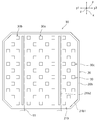
- FIG. 2 is a schematic plan view of the back surface of the solar cell according to the first embodiment.
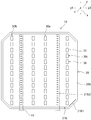
- FIG. 3 is a schematic plan view of the back surface of the solar cell according to the second embodiment.
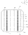
- FIG. 4 is a schematic plan view of the back surface of the solar cell according to the third embodiment.
- FIG. 5 is a schematic plan view of the back surface of the solar cell according to the fourth embodiment.
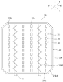
- FIG. 6 is a schematic plan view of the back surface of the solar cell according to the fifth embodiment.
- FIG. 7 is a schematic plan view of the back surface of the solar cell according to the sixth embodiment.
- FIG. 8 is a schematic plan view of the back surface of the solar cell according to the seventh embodiment.
- FIG. 1 is a schematic plan view of a light receiving surface of the solar cell according to the first embodiment.
- FIG. 2 is a schematic plan view of the back surface of the solar cell according to the first embodiment.
- FIG. 9 is a schematic plan view of the back surface of the solar cell according to the eighth embodiment.
- FIG. 10 is a schematic plan view of the back surface of the solar cell according to the ninth embodiment.
- FIG. 11 is a schematic plan view of the back surface of the solar cell according to the tenth embodiment.
- FIG. 12 is a schematic plan view of the back surface of the solar cell according to the eleventh embodiment.
- FIG. 1 is a schematic plan view of a light receiving surface of the solar cell according to the first embodiment.
- FIG. 2 is a schematic plan view of the back surface of the solar cell according to the first embodiment.
- the solar cell 10 has a photoelectric conversion unit 20.
- the photoelectric conversion unit 20 is a member that generates carriers such as electrons and holes by receiving light.
- the photoelectric conversion unit 20 is, for example, a substrate made of a crystalline semiconductor having one conductivity type, and a first amorphous semiconductor layer having another conductivity type disposed on one main surface of the substrate. And a second amorphous semiconductor layer having one conductivity type disposed on the other main surface of the substrate.
- an i-type amorphous semiconductor layer having a thickness that does not substantially contribute to power generation may be provided between at least one of the first and second amorphous semiconductor layers and the crystalline semiconductor substrate.
- the photoelectric conversion unit 20 may have a substrate in which an n-type dopant diffusion region and a p-type dopant diffusion region are exposed on the surface.
- the photoelectric conversion unit 20 has a light receiving surface 20a and a back surface 20b.
- Each of the light receiving surface 20a and the back surface 20b has a texture structure.
- the “texture structure” refers to a concavo-convex structure formed to suppress surface reflection and increase the light absorption amount of the photoelectric conversion unit.
- Specific examples of the texture structure include a pyramidal (quadrangular pyramid or quadrangular frustum-shaped) uneven structure obtained by performing anisotropic etching on the surface of a single crystal silicon substrate having a (100) plane. .
- texture structure is not limited to this, and isotropic etching such as wet etching using acid or dry etching is performed on the surface of a substrate made of a crystalline semiconductor such as single crystal silicon or polycrystalline silicon.
- isotropic etching such as wet etching using acid or dry etching is performed on the surface of a substrate made of a crystalline semiconductor such as single crystal silicon or polycrystalline silicon.
- the resulting uneven structure may be used.
- the light-receiving surface electrode 21a has a plurality of finger portions 21a1 and a plurality of bus bar portions 21a2.
- Each of the plurality of finger portions 21a1 has a line shape extending along the y direction.
- the plurality of finger portions 21a1 are arranged at predetermined intervals along the x direction.
- Each of the plurality of bus bar portions 21a2 extends along the x direction orthogonal to the y direction.
- Each of the plurality of bus bar portions 21a2 is electrically connected to the plurality of finger portions 21a1.
- the plurality of finger portions 21a1 collects carriers generated by the photoelectric conversion unit 20 by light reception.
- the bus bar portion 21a2 collects the carriers collected by the plurality of finger portions 21a1.
- the constituent material of the light receiving surface electrode 21a includes a metal.
- the light-receiving surface electrode 21a can be made of, for example, a metal such as silver, copper, aluminum, titanium, nickel, or chromium, or an alloy containing one or more of these metals.
- the light-receiving surface electrode 21a may be configured by a laminated body of a plurality of conductive layers made of the above metal or alloy, for example.
- the formation method of the light-receiving surface electrode 21a is not particularly limited.
- the light-receiving surface electrode 21a can be formed using a conductive paste such as an Ag paste, for example.
- the light receiving surface electrode 21a can be formed by using, for example, a sputtering method, a vapor deposition method, a screen printing method, a plating method, or the like.
- the back electrode 21b includes a metal film 21b1 and a plurality of connection electrodes 21b2.
- the back electrode 21b has a larger area than the light receiving surface electrode 21a. For this reason, the photoelectric conversion unit 20 can receive a lot of light.
- the “metal film” includes an alloy film.
- the metal film 21b1 is disposed on at least a part of the back surface 20b. Specifically, in the present embodiment, the metal film 21b1 is disposed on the inner region excluding the edge portion of the back surface 20b. The metal film 21b1 may be provided on the entire back surface 20b.
- the metal film 21b1 has such a thickness that unevenness having a shape corresponding to the texture structure exists on the surface opposite to the back surface 20b of the metal film 21b1.
- the thickness of the metal film 21b1 is preferably about 0.1 ⁇ m to 5 ⁇ m, for example.
- the constituent material of the metal film 21b1 is not particularly limited, but it is preferable that the metal film 21b1 has high light reflectivity and high conductivity.
- the metal film 21b1 can be made of a metal such as Ag, Al, Cu, Ni, Cr, Ti, Sn, Zn, or an alloy containing one or more of these metals.
- the metal film 21b1 may be configured by a laminated body of a plurality of films made of the above metals or alloys.
- the metal film 21b1 is disposed on the back surface 20b, and is disposed on the first Ag film having a thickness of about 0.1 ⁇ m to 1 ⁇ m and the first Ag film. It can be constituted by a laminate of an Al film having a thickness of about 0.1 ⁇ m to 1 ⁇ m and a second Ag film disposed on the Al film and having a thickness of about 0.1 ⁇ m to 1 ⁇ m.
- the formation method of the metal film 21b1 is not particularly limited.
- the metal film 21b1 can be formed using a conductive paste such as an Ag paste, for example.
- the metal film 21b1 can be formed using, for example, a sputtering method, a vapor deposition method, a screen printing method, an offset printing method, an ink jet method, a plating method, or the like.
- the metal film 21b1 may be formed directly on the back surface 20b, but a translucent conductive film may be provided between the metal film 21b1 and the back surface 20b. By providing the translucent conductive film, the adhesion to the back surface 20b of the metal film 21b1 can be improved.
- the translucent conductive film can be made of a translucent conductive oxide such as indium oxide or zinc oxide. The thickness of the translucent conductive film is preferably about 0.05 ⁇ m to 3 ⁇ m.
- connection electrodes 21b2 for electrical connection are disposed on the metal film 21b1.
- the plurality of connection electrodes 21b2 are arranged at intervals from each other along one direction (y direction).
- Each of the plurality of connection electrodes 21b2 is provided in a straight line extending in another direction (x direction) perpendicular to one direction (y direction).
- the number of connection electrodes 21b2 is preferably the same as the number of bus bar portions 21a2. Further, the connection electrode 21b2 is preferably provided in a positional relationship overlapping the bus bar portion 21a2. By doing in this way, the connection of the wiring material mentioned later becomes easy.
- the connection electrode 21b2 is an electrode that is electrically connected to the wiring member 11 when the solar cell module is configured by electrically connecting the plurality of solar cells 10 with the wiring member 11, for example. That is, by electrically connecting mainly the bus bar portion 21a2 of the light receiving surface electrode 21a of one solar cell 10 and the connection electrode 21b2 of the back surface electrode 21b of the other solar cell 10 by the wiring member 11, A solar cell string in which a plurality of solar cells 10 are electrically connected is configured.
- the solar cell string is configured by sealing the solar cell string with a protective member on the light receiving surface side, a protective member on the back surface side, and a filler layer filled between the protective members.
- the wiring material 11 and the solar cell 10 can be connected using solder or a resin adhesive.
- the connecting electrode 21b2 has a thickness protruding from the convex portion of the texture structure of the back surface 20b.
- the connection electrode 21b2 is preferably thicker than the metal film 21b1. Specifically, the thickness of the connection electrode 21b2 is preferably in the range of 5 ⁇ m to 30 ⁇ m.
- connection electrode 21b2 includes a metal.
- the connection electrode 21b2 can be made of, for example, a metal such as Cu, Ag, or Sn, or an alloy containing at least one of these metals. Further, the connection electrode 21b2 may be configured by a laminated body of a plurality of films made of the above metal or alloy.
- connection electrode 21b2 can be formed using, for example, a conductive paste such as an Ag paste.
- the connection electrode 21b2 can be formed using, for example, a sputtering method, a vapor deposition method, a screen printing method, a dispensing method, an offset printing method, an ink jet method, or the like.
- a plurality of convex portions 30 are arranged on the metal film 21b1.
- the plurality of convex portions 30 include a first convex portion 30a, a second convex portion 30b, and a third convex portion 30c.
- the first protrusion 30a is located between adjacent connection electrodes 21b2 in one direction (y direction).
- the 2nd convex part 30b is located in the one side (y1 side) in one direction (y direction) of the field in which a plurality of connection electrodes 21b2 were provided.
- the 3rd convex part 30c is located in the other side (y2 side) in one direction (y direction) of the field in which a plurality of connection electrodes 21b2 were provided.
- Each of the plurality of protrusions 30 includes a plurality of protrusions 31 arranged in a straight line at intervals in the x direction.
- the height of the convex portion 30 is preferably substantially the same as or higher than the height of the connection electrode 21b2.
- the width along the y direction of the convex portion 30 is preferably 1 to 10 times the width along the y direction of the connection electrode 21b2.
- the constituent material of the convex part 30 is not particularly limited.
- Specific examples of the convex portion 30 include, for example, resin and the same material as the connection electrode 21b2. By forming the convex part 30 with the same material as the connection electrode 21b2, the convex part 30 and the connection electrode 21b2 can be formed in the same process. Therefore, manufacture of the solar cell 10 becomes easy.
- Specific examples of the resin that is preferably used as the constituent material of the convex portion 30 include, for example, an epoxy resin, an acrylic resin, and a urethane resin.
- the metal film 21b1 is disposed.
- the metal film 21b1 covers at least a part of the back surface 20b. For this reason, the light which permeate
- the metal film 21b1 has such a thickness that unevenness having a shape corresponding to the texture structure exists on the surface opposite to the back surface 20b of the metal film 21b1. Therefore, the optical path length in the photoelectric conversion unit 20 of the light reflected by the metal film 21b1 can be increased. Therefore, more improved photoelectric conversion efficiency can be obtained.
- the thickness of the semiconductor substrate used for the photoelectric conversion unit 20 can be reduced to, for example, 180 ⁇ m or less.
- the thickness of the metal film 21b1 is preferably 0.1 ⁇ m or more. From the viewpoint of obtaining higher reliability, the thickness of the metal film 21b1 is preferably 5 ⁇ m or less.
- the connection electrode 21b2 is preferably thicker than the metal film 21b1. Specifically, the thickness of the connection electrode 21b2 is preferably 5 ⁇ m or more. However, if the thickness of the connection electrode 21b2 is too thick, the connection electrode 21b2 is easily peeled from the metal film 21b1 due to the stress of the connection electrode 21b2. Therefore, the thickness of the connection electrode 21b2 is preferably 20 ⁇ m or less.
- connection electrode 21b2 has a thickness protruding from the convex portion of the texture structure of the back surface 20b.
- connection electrode 21b2 extends from the one side end side in the x direction of the back surface 20b to the other side end side.
- the connection electrode 21b2 has a length of about 70% or more of the length of the photoelectric conversion unit 20. For this reason, even when a stress is generated between the wiring member 11 and the connection electrode 21b2 due to a temperature change or the like, the stress per unit area can be reduced. Therefore, peeling of the wiring material 11 can be suppressed more effectively.
- the back surface 20b has a texture structure. For this reason, light is scattered on the back surface 20b, and the light is easily confined in the photoelectric conversion unit 20, so that more improved photoelectric conversion efficiency can be obtained.
- the metal film 21b1 has such a thickness that unevenness having a shape corresponding to the texture structure exists on the surface opposite to the back surface 20b of the metal film 21b1. For this reason, the adhesion strength between the metal film 21b1 and the connection electrode 21b2 can be increased.
- connection electrode 21b2 protrudes from the back surface 20b. For this reason, for example, when the solar cell 10 is in contact with another member during the process after the electrode forming step of the solar cell 10 or during the conveyance, a large stress may be concentrated on the connection electrode 21b2. . As a result, damage such as peeling may occur in a part of the connection electrode 21b2.
- connection electrode 21b2 In contrast, in the solar cell 10, a plurality of convex portions 30 including the first convex portions 30a located between the adjacent connection electrodes 21b2 are provided. For this reason, even when the solar cell 10 comes into contact with another member during the transportation of the solar cell 10, stress is distributed and applied to the connection electrode 21 b 2 and the convex portion 30. Therefore, it is possible to suppress a large stress from being concentrated on the connection electrode 21b2. Therefore, damage to the connection electrode 21b2 can be suppressed.
- the second and third electrodes are provided on both sides of the region where the plurality of connection electrodes 21b2 are provided. Protrusions 30b and 30c are provided. For this reason, it can suppress more effectively that a big stress is intensively added to the electrode 21b2 for a connection. Therefore, damage to the connection electrode 21b2 can be more effectively suppressed.
- the convex portion 30 is arranged between the adjacent connection electrodes 21b2, when the external stress in the direction from the light receiving surface 20a to the back surface 20b is generated between the adjacent connection electrodes 21b2, the convex portion 30 is photoelectric. It works as a support for the conversion unit 20 and can suppress damage such as cracking of the solar cell 10.
- the convex part 30 is resin, the elasticity of the convex part 30 becomes high. For this reason, it can suppress more effectively that big stress is intensively applied to the electrode 21b2 for connection, and can also suppress effectively that stress is applied to the photoelectric conversion part 20 via the convex part 30. FIG. Therefore, damage to the solar cell 10 can be suppressed more effectively.
- the convex part 30 is lower than the connection electrode 21b2, an effect that it is possible to suppress a large stress from being concentrated on the connection electrode 21b2 described above can be obtained, but the effect is further enhanced.
- the height of the convex portion 30 is preferably equal to or higher than the height of the connection electrode 21b2.
- FIG. 3 is a schematic plan view of the back surface of the solar cell according to the second embodiment.
- FIG. 4 is a schematic plan view of the back surface of the solar cell according to the third embodiment.
- FIG. 5 is a schematic plan view of the back surface of the solar cell according to the fourth embodiment.
- FIG. 6 is a schematic plan view of the back surface of the solar cell according to the fifth embodiment.
- FIG. 7 is a schematic plan view of the back surface of the solar cell according to the sixth embodiment.
- each of the plurality of protrusions 30 is configured by a plurality of protrusions 31 arranged at intervals along the x direction.
- the shape of the convex portion 30 is not particularly limited.
- the arrangement of the plurality of convex portions 30 is not particularly limited.
- each of the plurality of convex portions 30 may be a linear convex portion extending along another direction (x direction) perpendicular to one direction (y direction).
- the plurality of convex portions 30 may be configured by a plurality of linear convex portions that are arranged along the x direction and extend along the y direction.
- the convex part 30 is dot-shaped, and the plurality of convex parts 30 may be arranged in a square matrix. Moreover, as shown in FIG. 6, the convex part 30 is dot shape, and the some convex part 30 may be distribute
- the convex part 30 may be zigzag-shaped.
- FIG. 8 is a schematic plan view of the back surface of the solar cell according to the seventh embodiment.
- FIG. 9 is a schematic plan view of the back surface of the solar cell according to the eighth embodiment.
- FIG. 10 is a schematic plan view of the back surface of the solar cell according to the ninth embodiment.
- FIG. 11 is a schematic plan view of the back surface of the solar cell according to the tenth embodiment.
- FIG. 12 is a schematic plan view of the back surface of the solar cell according to the eleventh embodiment.
- connection electrode 21b2 is a linear electrode extending in the x direction.
- shape of the connection electrode is not particularly limited.
- connection electrodes 21b2 may be configured by a plurality of linear electrodes arranged along the x direction and extending along the y direction.
- connection electrodes 21 b 2 are arranged along the x direction, and each crosses the first linear electrode portion extending along the y direction and the first linear electrode portion. And a plurality of electrodes including a plurality of second linear electrode portions extending along the x direction.
- connection electrode 21b2 may be composed of a plurality of V-shaped electrodes arranged along the x direction.
- connection electrode 21b2 may be composed of a plurality of linear electrodes arranged in a matrix.
- connection electrode 21b2 may be formed of a zigzag electrode.
- the convex portion 30 may be the convex portion described in the second to sixth embodiments.
- the light-receiving surface electrode may be a so-called bus bar-less electrode that includes only a plurality of finger portions and does not have a bus bar portion.
- only one connection electrode may be provided, or three or more connection electrodes may be provided along the y direction.
- the shapes of the first to third convex portions may be different from each other.
Abstract
Provided is a solar cell having improved photoelectric conversion efficiency.
A solar cell (10) comprises a photoelectric conversion unit (20), a light-receiving surface electrode (21a) which is arranged on a light-receiving surface (20a) and contains a metal, and a back surface electrode (21b) which is arranged on a back surface (20b) and contains a metal. The back surface electrode (21b) comprises a metal film (21b1) and multiple connection electrodes (21b2). The metal film (21b1) is arranged on at least a part of the back surface (20b). The multiple connection electrodes (21b2) are arranged on the metal film (21b1). The multiple connection electrodes (21b2) are arrayed along one direction (y). The solar cell (10) additionally comprises a first projected part (30a). The first projected part (30a) is located between any two of the connection electrodes (21b2) which are adjacent to each other in the one direction (y).
Description
本発明は、太陽電池に関する。
The present invention relates to a solar cell.
特許文献1には、光電変換部と、光電変換部の受光面の上に配された受光面電極と、裏面の上に配された裏面電極とを備える太陽電池が記載されている。この太陽電池では、受光面電極及び裏面電極のそれぞれが、複数のフィンガー部と、複数のフィンガー部に電気的に接続されているバスバー部とを備えている。
Patent Document 1 describes a solar cell including a photoelectric conversion unit, a light receiving surface electrode disposed on a light receiving surface of the photoelectric conversion unit, and a back electrode disposed on a back surface. In this solar cell, each of the light-receiving surface electrode and the back surface electrode includes a plurality of finger portions and a bus bar portion electrically connected to the plurality of finger portions.
近年、太陽電池の光電変換効率をさらに向上したいという要望が高まってきている。
In recent years, there is an increasing demand for further improving the photoelectric conversion efficiency of solar cells.
本発明は、斯かる点に鑑みて成されたものであり、その目的は、改善された光電変換効率を有する太陽電池を提供することにある。
The present invention has been made in view of such a point, and an object thereof is to provide a solar cell having improved photoelectric conversion efficiency.
本発明に係る太陽電池は、光電変換部と、受光面電極と、裏面電極とを備えている。光電変換部は、受光面及び裏面を有する。受光面電極は、受光面の上に配されている。受光面電極は、金属を含む。裏面電極は、裏面の上に配されている。裏面電極は、金属を含む。裏面電極は、金属膜と、複数の接続用電極とを含む。金属膜は、裏面の少なくとも一部の上に配されている。複数の接続用電極は、金属膜の上に配されている。複数の接続用電極は、一の方向に沿って相互に間隔をおいて配列されている。本発明に係る太陽電池は、第1の凸部をさらに備えている。第1の凸部は、一の方向において隣り合う接続用電極の間に位置している。
The solar cell according to the present invention includes a photoelectric conversion unit, a light receiving surface electrode, and a back electrode. The photoelectric conversion unit has a light receiving surface and a back surface. The light receiving surface electrode is disposed on the light receiving surface. The light-receiving surface electrode contains a metal. The back electrode is arranged on the back surface. The back electrode includes a metal. The back electrode includes a metal film and a plurality of connection electrodes. The metal film is disposed on at least a part of the back surface. The plurality of connection electrodes are arranged on the metal film. The plurality of connection electrodes are arranged at intervals from one another along one direction. The solar cell according to the present invention further includes a first convex portion. The 1st convex part is located between the connection electrodes adjacent in one direction.
本発明によれば、改善された光電変換効率を有する太陽電池を提供することができる。
According to the present invention, a solar cell having improved photoelectric conversion efficiency can be provided.
以下、本発明を実施した好ましい形態の一例について説明する。但し、以下の実施形態は、単なる例示である。本発明は、以下の実施形態に何ら限定されない。
Hereinafter, an example of a preferable embodiment in which the present invention is implemented will be described. However, the following embodiments are merely examples. The present invention is not limited to the following embodiments.
実施形態等において参照する各図面において、実質的に同一の機能を有する部材は同一の符号で参照することとする。また、実施形態等において参照する図面は、模式的に記載されたものであり、図面に描画された物体の寸法の比率などは、現実の物体の寸法の比率などとは異なる場合がある。図面相互間においても、物体の寸法比率等が異なる場合がある。具体的な物体の寸法比率等は、以下の説明を参酌して判断されるべきである。
In each drawing referred to in the embodiment or the like, members having substantially the same function are referred to by the same reference numerals. The drawings referred to in the embodiments and the like are schematically described, and the ratio of the dimensions of the objects drawn in the drawings may be different from the ratio of the dimensions of the actual objects. The dimensional ratio of the object may be different between the drawings. The specific dimensional ratio of the object should be determined in consideration of the following description.
《第1の実施形態》
図1は、第1の実施形態に係る太陽電池の受光面の略図的平面図である。図2は、第1の実施形態に係る太陽電池の裏面の略図的平面図である。 << First Embodiment >>
FIG. 1 is a schematic plan view of a light receiving surface of the solar cell according to the first embodiment. FIG. 2 is a schematic plan view of the back surface of the solar cell according to the first embodiment.
太陽電池10は、光電変換部20を有する。光電変換部20は、受光することによって電子や正孔などのキャリアを生成させる部材である。光電変換部20は、例えば、一の導電型を有する結晶性半導体からなる基板と、その基板の一の主面上に配されており、他の導電型を有する第1の非晶質半導体層と、基板の他の主面上に配されており、一の導電型を有する第2の非晶質半導体層とを有するものであってもよい。その場合において、第1及び第2の非晶質半導体層の少なくとも一方と、結晶性半導体基板との間に、実質的に発電に寄与しない厚みのi型非晶質半導体層を設けてもよい。また、光電変換部20は、n型ドーパント拡散領域とp型ドーパント拡散領域とが表面に露出している基板を有するものであってもよい。
The solar cell 10 has a photoelectric conversion unit 20. The photoelectric conversion unit 20 is a member that generates carriers such as electrons and holes by receiving light. The photoelectric conversion unit 20 is, for example, a substrate made of a crystalline semiconductor having one conductivity type, and a first amorphous semiconductor layer having another conductivity type disposed on one main surface of the substrate. And a second amorphous semiconductor layer having one conductivity type disposed on the other main surface of the substrate. In that case, an i-type amorphous semiconductor layer having a thickness that does not substantially contribute to power generation may be provided between at least one of the first and second amorphous semiconductor layers and the crystalline semiconductor substrate. . Further, the photoelectric conversion unit 20 may have a substrate in which an n-type dopant diffusion region and a p-type dopant diffusion region are exposed on the surface.
光電変換部20は、受光面20aと裏面20bとを有する。受光面20a及び裏面20bのそれぞれは、テクスチャ構造を有する。ここで、「テクスチャ構造」とは、表面反射を抑制し、光電変換部の光吸収量を増大させるために形成されている凹凸構造のことをいう。テクスチャ構造の具体例としては、(100)面を有する単結晶シリコン基板の表面に異方性エッチングを施すことによって得られるピラミッド状(四角錐状や、四角錐台状)の凹凸構造が挙げられる。なお、テクスチャ構造は、これに限定されず、単結晶シリコン或いは多結晶シリコン等の結晶性半導体からなる基板の表面に、酸を用いたウェットエッチングやドライエッチング等による等方性エッチングを施すことによって得られる凹凸構造であってもよい。
The photoelectric conversion unit 20 has a light receiving surface 20a and a back surface 20b. Each of the light receiving surface 20a and the back surface 20b has a texture structure. Here, the “texture structure” refers to a concavo-convex structure formed to suppress surface reflection and increase the light absorption amount of the photoelectric conversion unit. Specific examples of the texture structure include a pyramidal (quadrangular pyramid or quadrangular frustum-shaped) uneven structure obtained by performing anisotropic etching on the surface of a single crystal silicon substrate having a (100) plane. . Note that the texture structure is not limited to this, and isotropic etching such as wet etching using acid or dry etching is performed on the surface of a substrate made of a crystalline semiconductor such as single crystal silicon or polycrystalline silicon. The resulting uneven structure may be used.
光電変換部20の受光面20aの上には、金属を含む受光面電極21aが配されている。受光面電極21aは、複数のフィンガー部21a1と、複数のバスバー部21a2とを有する。複数のフィンガー部21a1のそれぞれは、y方向に沿って延びるライン状の形状を有する。複数のフィンガー部21a1は、x方向に沿って所定の間隔を隔てて配列されている。複数のバスバー部21a2のそれぞれは、y方向と直交するx方向に沿って延びている。複数のバスバー部21a2のそれぞれは、複数のフィンガー部21a1に電気的に接続されている。複数のフィンガー部21a1は、受光により光電変換部20で生成されたキャリアを収集する。バスバー部21a2は、複数のフィンガー部21a1で収集されたキャリアを集電する。
On the light receiving surface 20a of the photoelectric conversion unit 20, a light receiving surface electrode 21a containing metal is disposed. The light-receiving surface electrode 21a has a plurality of finger portions 21a1 and a plurality of bus bar portions 21a2. Each of the plurality of finger portions 21a1 has a line shape extending along the y direction. The plurality of finger portions 21a1 are arranged at predetermined intervals along the x direction. Each of the plurality of bus bar portions 21a2 extends along the x direction orthogonal to the y direction. Each of the plurality of bus bar portions 21a2 is electrically connected to the plurality of finger portions 21a1. The plurality of finger portions 21a1 collects carriers generated by the photoelectric conversion unit 20 by light reception. The bus bar portion 21a2 collects the carriers collected by the plurality of finger portions 21a1.
受光面電極21aの構成材料は、金属を含む。受光面電極21aは、例えば、銀、銅、アルミニウム、チタン、ニッケル、クロムなどの金属や、それらの金属のうちの一種以上を含む合金により構成することができる。また、受光面電極21aは、例えば、上記金属や合金からなる複数の導電層の積層体により構成されていてもよい。
The constituent material of the light receiving surface electrode 21a includes a metal. The light-receiving surface electrode 21a can be made of, for example, a metal such as silver, copper, aluminum, titanium, nickel, or chromium, or an alloy containing one or more of these metals. Moreover, the light-receiving surface electrode 21a may be configured by a laminated body of a plurality of conductive layers made of the above metal or alloy, for example.
受光面電極21aの形成方法は、特に限定されない。受光面電極21aは、例えば、Agペースト等の導電性ペーストを用いて形成することができる。また、受光面電極21aは、例えば、スパッタ法、蒸着法、スクリーン印刷法、或いはメッキ法等を用いて形成することができる。
The formation method of the light-receiving surface electrode 21a is not particularly limited. The light-receiving surface electrode 21a can be formed using a conductive paste such as an Ag paste, for example. The light receiving surface electrode 21a can be formed by using, for example, a sputtering method, a vapor deposition method, a screen printing method, a plating method, or the like.
光電変換部20の裏面20bの上には、金属を含む裏面電極21bが配されている。裏面電極21bは、金属膜21b1と、複数の接続用電極21b2とを含む。裏面電極21bは、受光面電極21aより広い面積を有する。このため、光電変換部20は、多くの光を受光することができる。
On the back surface 20b of the photoelectric conversion unit 20, a back electrode 21b containing metal is disposed. The back electrode 21b includes a metal film 21b1 and a plurality of connection electrodes 21b2. The back electrode 21b has a larger area than the light receiving surface electrode 21a. For this reason, the photoelectric conversion unit 20 can receive a lot of light.
本実施形態において、「金属膜」には、合金膜が含まれるものとする。
In this embodiment, the “metal film” includes an alloy film.
金属膜21b1は、裏面20bの少なくとも一部の上に配されている。具体的には、本実施形態では、金属膜21b1は、裏面20bの端縁部を除く内側領域の上に配されている。金属膜21b1は、裏面20bの全面上に設けられていてもよい。
The metal film 21b1 is disposed on at least a part of the back surface 20b. Specifically, in the present embodiment, the metal film 21b1 is disposed on the inner region excluding the edge portion of the back surface 20b. The metal film 21b1 may be provided on the entire back surface 20b.
金属膜21b1は、金属膜21b1の裏面20bとは反対側の表面にテクスチャ構造に対応した形状の凹凸が存するような厚みを有する。具体的には、金属膜21b1の厚みは、例えば、0.1μm~5μm程度であることが好ましい。
The metal film 21b1 has such a thickness that unevenness having a shape corresponding to the texture structure exists on the surface opposite to the back surface 20b of the metal film 21b1. Specifically, the thickness of the metal film 21b1 is preferably about 0.1 μm to 5 μm, for example.
金属膜21b1の構成材料は、特に限定されないが、光反射率が高く、かつ、高い導電性を有するものであることが好ましい。このため、金属膜21b1は、Ag、Al、Cu、Ni、Cr、Ti、Sn、Znなどの金属や、それらの金属の一種以上を含む合金により構成することができる。また、金属膜21b1は、上記金属や合金からなる複数の膜の積層体により構成されていてもよい。金属膜21b1は、具体的には、例えば、裏面20bの上に配されており、厚みが0.1μm~1μm程度の第1のAg膜と、第1のAg膜の上に配されており、厚みが0.1μm~1μm程度のAl膜と、Al膜の上に配されており、厚みが0.1μm~1μm程度の第2のAg膜との積層体により構成することができる。
The constituent material of the metal film 21b1 is not particularly limited, but it is preferable that the metal film 21b1 has high light reflectivity and high conductivity. For this reason, the metal film 21b1 can be made of a metal such as Ag, Al, Cu, Ni, Cr, Ti, Sn, Zn, or an alloy containing one or more of these metals. Moreover, the metal film 21b1 may be configured by a laminated body of a plurality of films made of the above metals or alloys. Specifically, for example, the metal film 21b1 is disposed on the back surface 20b, and is disposed on the first Ag film having a thickness of about 0.1 μm to 1 μm and the first Ag film. It can be constituted by a laminate of an Al film having a thickness of about 0.1 μm to 1 μm and a second Ag film disposed on the Al film and having a thickness of about 0.1 μm to 1 μm.
金属膜21b1の形成方法は特に限定されない。金属膜21b1は、例えば、Agペースト等の導電性ペーストを用いて形成することができる。また、金属膜21b1は、例えば、スパッタ法、蒸着法、スクリーン印刷法、オフセット印刷法、インクジェット法、或いはメッキ法等を用いて形成することができる。
The formation method of the metal film 21b1 is not particularly limited. The metal film 21b1 can be formed using a conductive paste such as an Ag paste, for example. The metal film 21b1 can be formed using, for example, a sputtering method, a vapor deposition method, a screen printing method, an offset printing method, an ink jet method, a plating method, or the like.
金属膜21b1は、裏面20bの上に直接形成してもよいが、金属膜21b1と裏面20bとの間に透光性導電膜を設けてもよい。透光性導電膜を設けることにより、金属膜21b1の裏面20bに対する密着性を高めることができる。透光性導電膜は、例えば、酸化インジウムや酸化亜鉛等の透光性導電酸化物により構成することができる。透光性導電膜の厚みは、0.05μm~3μm程度であることが好ましい。
The metal film 21b1 may be formed directly on the back surface 20b, but a translucent conductive film may be provided between the metal film 21b1 and the back surface 20b. By providing the translucent conductive film, the adhesion to the back surface 20b of the metal film 21b1 can be improved. The translucent conductive film can be made of a translucent conductive oxide such as indium oxide or zinc oxide. The thickness of the translucent conductive film is preferably about 0.05 μm to 3 μm.
金属膜21b1の上には、複数の電気的接続用の接続用電極21b2が配されている。複数の接続用電極21b2は、一の方向(y方向)に沿って相互に間隔をおいて配列されている。複数の接続用電極21b2のそれぞれは、一の方向(y方向)に対して垂直な他の方向(x方向)に延びる直線状に設けられている。接続用電極21b2の数は、バスバー部21a2の数と同じにすることが好ましい。また、接続用電極21b2は、バスバー部21a2と重なる位置関係に設けることが好ましい。このようにすることで、後述する配線材の接続が容易になる。
A plurality of connection electrodes 21b2 for electrical connection are disposed on the metal film 21b1. The plurality of connection electrodes 21b2 are arranged at intervals from each other along one direction (y direction). Each of the plurality of connection electrodes 21b2 is provided in a straight line extending in another direction (x direction) perpendicular to one direction (y direction). The number of connection electrodes 21b2 is preferably the same as the number of bus bar portions 21a2. Further, the connection electrode 21b2 is preferably provided in a positional relationship overlapping the bus bar portion 21a2. By doing in this way, the connection of the wiring material mentioned later becomes easy.
接続用電極21b2は、例えば配線材11により複数の太陽電池10を電気的に接続して太陽電池モジュールを構成する際に、配線材11と電気的に接続される電極である。すなわち、一の太陽電池10の受光面電極21aの主としてバスバー部21a2と、他の太陽電池10の裏面電極21bの主として接続用電極21b2とを配線材11により電気的に接続していくことにより、複数の太陽電池10が電気的に接続された太陽電池ストリングが構成される。その太陽電池ストリングを、受光面側の保護部材と、裏面側の保護部材と、両保護部材の間に充填された充填材層とにより封止することにより太陽電池モジュールが構成される。なお、配線材11と太陽電池10との接続は、半田や樹脂接着剤を用いて行うことができる。
The connection electrode 21b2 is an electrode that is electrically connected to the wiring member 11 when the solar cell module is configured by electrically connecting the plurality of solar cells 10 with the wiring member 11, for example. That is, by electrically connecting mainly the bus bar portion 21a2 of the light receiving surface electrode 21a of one solar cell 10 and the connection electrode 21b2 of the back surface electrode 21b of the other solar cell 10 by the wiring member 11, A solar cell string in which a plurality of solar cells 10 are electrically connected is configured. The solar cell string is configured by sealing the solar cell string with a protective member on the light receiving surface side, a protective member on the back surface side, and a filler layer filled between the protective members. The wiring material 11 and the solar cell 10 can be connected using solder or a resin adhesive.
接続用電極21b2は、裏面20bのテクスチャ構造が有する凸部から突出する厚みを有する。接続用電極21b2は、金属膜21b1よりも厚いことが好ましい。具体的には、接続用電極21b2の厚みは、5μm~30μmの範囲内にあることが好ましい。
The connecting electrode 21b2 has a thickness protruding from the convex portion of the texture structure of the back surface 20b. The connection electrode 21b2 is preferably thicker than the metal film 21b1. Specifically, the thickness of the connection electrode 21b2 is preferably in the range of 5 μm to 30 μm.
接続用電極21b2の構成材料は、金属を含む。接続用電極21b2は、例えば、Cu、Ag、Sn等の金属や、それらの金属の少なくとも一種を含む合金により構成することができる。また、接続用電極21b2は、上記金属や合金からなる複数の膜の積層体により構成されていてもよい。
The constituent material of the connection electrode 21b2 includes a metal. The connection electrode 21b2 can be made of, for example, a metal such as Cu, Ag, or Sn, or an alloy containing at least one of these metals. Further, the connection electrode 21b2 may be configured by a laminated body of a plurality of films made of the above metal or alloy.
接続用電極21b2の形成方法は特に限定されない。接続用電極21b2は、例えば、Agペースト等の導電性ペーストを用いて形成することができる。また、接続用電極21b2は、例えば、スパッタ法、蒸着法、スクリーン印刷法、ディスペンス法、オフセット印刷法、インクジェット法等を用いて形成することができる。
The method for forming the connection electrode 21b2 is not particularly limited. The connection electrode 21b2 can be formed using, for example, a conductive paste such as an Ag paste. The connection electrode 21b2 can be formed using, for example, a sputtering method, a vapor deposition method, a screen printing method, a dispensing method, an offset printing method, an ink jet method, or the like.
太陽電池10では、金属膜21b1の上に、複数の凸部30が配されている。複数の凸部30は、第1の凸部30aと、第2の凸部30bと、第3の凸部30cとを含む。第1の凸部30aは、一の方向(y方向)において隣り合う接続用電極21b2の間に位置している。第2の凸部30bは、複数の接続用電極21b2が設けられた領域の一の方向(y方向)における一方側(y1側)に位置している。第3の凸部30cは、複数の接続用電極21b2が設けられた領域の一の方向(y方向)における他方側(y2側)に位置している。
In the solar cell 10, a plurality of convex portions 30 are arranged on the metal film 21b1. The plurality of convex portions 30 include a first convex portion 30a, a second convex portion 30b, and a third convex portion 30c. The first protrusion 30a is located between adjacent connection electrodes 21b2 in one direction (y direction). The 2nd convex part 30b is located in the one side (y1 side) in one direction (y direction) of the field in which a plurality of connection electrodes 21b2 were provided. The 3rd convex part 30c is located in the other side (y2 side) in one direction (y direction) of the field in which a plurality of connection electrodes 21b2 were provided.
複数の凸部30のそれぞれは、x方向に沿って相互に間隔をおいて直線状に配列されている複数の凸部31を含む。
Each of the plurality of protrusions 30 includes a plurality of protrusions 31 arranged in a straight line at intervals in the x direction.
凸部30の高さは、接続用電極21b2の高さと略同一か、またはそれ以上であることが好ましい。
The height of the convex portion 30 is preferably substantially the same as or higher than the height of the connection electrode 21b2.
凸部30のy方向に沿った幅は、接続用電極21b2のy方向に沿った幅の1倍以上10倍以下であることが好ましい。
The width along the y direction of the convex portion 30 is preferably 1 to 10 times the width along the y direction of the connection electrode 21b2.
凸部30の構成材料は、特に限定されない。凸部30の具体例としては、例えば、樹脂や、接続用電極21b2と同じ材料が挙げられる。凸部30を接続用電極21b2と同じ材料により構成することにより、凸部30と接続用電極21b2とを同一工程で形成できる。従って、太陽電池10の製造が容易となる。凸部30の構成材料として好ましく用いられる樹脂の具体例としては例えば、エポキシ系の樹脂、アクリル系の樹脂、ウレタン系の樹脂が挙げられる。
The constituent material of the convex part 30 is not particularly limited. Specific examples of the convex portion 30 include, for example, resin and the same material as the connection electrode 21b2. By forming the convex part 30 with the same material as the connection electrode 21b2, the convex part 30 and the connection electrode 21b2 can be formed in the same process. Therefore, manufacture of the solar cell 10 becomes easy. Specific examples of the resin that is preferably used as the constituent material of the convex portion 30 include, for example, an epoxy resin, an acrylic resin, and a urethane resin.
以上説明したように、本実施形態では、金属膜21b1が配されている。そして、その金属膜21b1により裏面20bの少なくとも一部が覆われている。このため、光電変換部20を透過した光が金属膜21b1によって受光面20a側に反射される。よって、光の有効利用を図ることができる。
As described above, in the present embodiment, the metal film 21b1 is disposed. The metal film 21b1 covers at least a part of the back surface 20b. For this reason, the light which permeate | transmitted the photoelectric conversion part 20 is reflected by the light-receiving surface 20a side by the metal film 21b1. Therefore, effective use of light can be achieved.
また、金属膜21b1は、金属膜21b1の裏面20bとは反対側の表面にテクスチャ構造に対応した形状の凹凸が存するような厚みを有する。よって、金属膜21b1で反射された光の光電変換部20における光路長を長くすることができる。従って、より改善された光電変換効率を得ることができる。
Further, the metal film 21b1 has such a thickness that unevenness having a shape corresponding to the texture structure exists on the surface opposite to the back surface 20b of the metal film 21b1. Therefore, the optical path length in the photoelectric conversion unit 20 of the light reflected by the metal film 21b1 can be increased. Therefore, more improved photoelectric conversion efficiency can be obtained.
また、熱膨張係数の違いに起因して生じる金属膜21b1から光電変換部20へのストレスを低減することができる。その結果、光電変換部20に用いる半導体の基板の厚みを例えば180μm以下といった薄い厚みにすることができる。
Further, it is possible to reduce the stress from the metal film 21b1 caused by the difference in the thermal expansion coefficient to the photoelectric conversion unit 20. As a result, the thickness of the semiconductor substrate used for the photoelectric conversion unit 20 can be reduced to, for example, 180 μm or less.
より改善された光電変換効率を得る観点からは、金属膜21b1の厚みは、0.1μm以上であることが好ましい。より高い信頼性を得る観点からは、金属膜21b1の厚みは、5μm以下であることが好ましい。
From the viewpoint of obtaining more improved photoelectric conversion efficiency, the thickness of the metal film 21b1 is preferably 0.1 μm or more. From the viewpoint of obtaining higher reliability, the thickness of the metal film 21b1 is preferably 5 μm or less.
また接続用電極21b2と配線材11との接続をより確実なものにする観点からは、接続用電極21b2は、金属膜21b1よりも厚いことが好ましい。具体的には、接続用電極21b2の厚みは、5μm以上であることが好ましい。但し、接続用電極21b2の厚みが厚すぎると、接続用電極21b2の応力により金属膜21b1から剥離しやすくなる。従って、接続用電極21b2の厚みは、20μm以下であることが好ましい。
Further, from the viewpoint of ensuring the connection between the connection electrode 21b2 and the wiring member 11, the connection electrode 21b2 is preferably thicker than the metal film 21b1. Specifically, the thickness of the connection electrode 21b2 is preferably 5 μm or more. However, if the thickness of the connection electrode 21b2 is too thick, the connection electrode 21b2 is easily peeled from the metal film 21b1 due to the stress of the connection electrode 21b2. Therefore, the thickness of the connection electrode 21b2 is preferably 20 μm or less.
また、接続用電極21b2は、裏面20bのテクスチャ構造が有する凸部から突出する厚みを有することが好ましい。このようにすることで、接続用電極21b2と配線材11との接続をより確実なものとすることができる。特に、樹脂接着剤を用いて配線材11を接続電極21b2に接続する場合に、両者の接続をより確実なものとすることができる。
Further, it is preferable that the connection electrode 21b2 has a thickness protruding from the convex portion of the texture structure of the back surface 20b. By doing in this way, connection with the electrode 21b2 for a connection and the wiring material 11 can be made more reliable. In particular, when the wiring member 11 is connected to the connection electrode 21b2 using a resin adhesive, the connection between the two can be made more reliable.
本実施形態では、接続用電極21b2は、裏面20bのx方向における一方側端側から他方側端側に延びている。接続用電極21b2は、光電変換部20の長さの約70%以上の長さを有する。このため、温度変化などに起因して配線材11と接続用電極21b2との間に応力が生じた場合であっても、単位面積あたりの応力を小さくすることができる。従って、配線材11の剥離をより効果的に抑制することができる。
In the present embodiment, the connection electrode 21b2 extends from the one side end side in the x direction of the back surface 20b to the other side end side. The connection electrode 21b2 has a length of about 70% or more of the length of the photoelectric conversion unit 20. For this reason, even when a stress is generated between the wiring member 11 and the connection electrode 21b2 due to a temperature change or the like, the stress per unit area can be reduced. Therefore, peeling of the wiring material 11 can be suppressed more effectively.
本実施形態では、裏面20bがテクスチャ構造を有する。このため、裏面20bにおいて光が散乱し、光電変換部20内に光が閉じ込められやすくなるため、より改善された光電変換効率を得ることができる。
In the present embodiment, the back surface 20b has a texture structure. For this reason, light is scattered on the back surface 20b, and the light is easily confined in the photoelectric conversion unit 20, so that more improved photoelectric conversion efficiency can be obtained.
さらに、金属膜21b1が、金属膜21b1の裏面20bとは反対側の表面にテクスチャ構造に対応した形状の凹凸が存するような厚みを有する。このため、金属膜21b1と接続用電極21b2との密着強度を高めることができる。
Furthermore, the metal film 21b1 has such a thickness that unevenness having a shape corresponding to the texture structure exists on the surface opposite to the back surface 20b of the metal film 21b1. For this reason, the adhesion strength between the metal film 21b1 and the connection electrode 21b2 can be increased.
ところで、凸部30を設けない場合は、接続用電極21b2のみが裏面20bから突出することとなる。このため、例えば、太陽電池10の電極形成工程以降の工程処理中、搬送途中などにおいて太陽電池10が他の部材と接触した場合に、接続用電極21b2に大きな応力が集中的に加わる虞がある。この結果、接続用電極21b2の一部に、剥がれ等の損傷が生じる可能性がある。
By the way, when the convex portion 30 is not provided, only the connection electrode 21b2 protrudes from the back surface 20b. For this reason, for example, when the solar cell 10 is in contact with another member during the process after the electrode forming step of the solar cell 10 or during the conveyance, a large stress may be concentrated on the connection electrode 21b2. . As a result, damage such as peeling may occur in a part of the connection electrode 21b2.
それに対して、太陽電池10では、隣り合う接続用電極21b2の間に位置している第1の凸部30aを含む複数の凸部30が設けられている。このため、太陽電池10の搬送途中などにおいて太陽電池10が他の部材と接触した場合においても、接続用電極21b2と凸部30とに応力が分散して加わる。よって、接続用電極21b2に大きな応力が集中的に加わることを抑制することができる。従って、接続用電極21b2の損傷を抑制することができる。
In contrast, in the solar cell 10, a plurality of convex portions 30 including the first convex portions 30a located between the adjacent connection electrodes 21b2 are provided. For this reason, even when the solar cell 10 comes into contact with another member during the transportation of the solar cell 10, stress is distributed and applied to the connection electrode 21 b 2 and the convex portion 30. Therefore, it is possible to suppress a large stress from being concentrated on the connection electrode 21b2. Therefore, damage to the connection electrode 21b2 can be suppressed.
また、本実施形態では、隣り合う接続用電極21b2の間に位置している第1の凸部30aに加えて、複数の接続用電極21b2が設けられた領域の両側に第2及び第3の凸部30b、30cが設けられている。このため、接続用電極21b2に大きな応力が集中的に加わることをより効果的に抑制することができる。従って、接続用電極21b2の損傷をより効果的に抑制することができる。
In the present embodiment, in addition to the first convex portion 30a located between the adjacent connection electrodes 21b2, the second and third electrodes are provided on both sides of the region where the plurality of connection electrodes 21b2 are provided. Protrusions 30b and 30c are provided. For this reason, it can suppress more effectively that a big stress is intensively added to the electrode 21b2 for a connection. Therefore, damage to the connection electrode 21b2 can be more effectively suppressed.
また、隣り合う接続用電極21b2の間に凸部30が配置されていることにより隣り合う接続用電極21b2間に受光面20aから裏面20b方向の外部応力が発生した場合において、凸部30は光電変換部20の支持体として働き、太陽電池10の割れ等の損傷を抑制することが可能となる。
Further, since the convex portion 30 is arranged between the adjacent connection electrodes 21b2, when the external stress in the direction from the light receiving surface 20a to the back surface 20b is generated between the adjacent connection electrodes 21b2, the convex portion 30 is photoelectric. It works as a support for the conversion unit 20 and can suppress damage such as cracking of the solar cell 10.
また、凸部30が樹脂製である場合は、凸部30の弾性が高くなる。このため、接続用電極21b2に大きな応力が集中的に加わることをさらに効果的に抑制できると共に、凸部30を介して光電変換部20に応力が加わることも効果的に抑制することができる。従って、太陽電池10の損傷をより効果的に抑制することができる。
Moreover, when the convex part 30 is resin, the elasticity of the convex part 30 becomes high. For this reason, it can suppress more effectively that big stress is intensively applied to the electrode 21b2 for connection, and can also suppress effectively that stress is applied to the photoelectric conversion part 20 via the convex part 30. FIG. Therefore, damage to the solar cell 10 can be suppressed more effectively.
なお、凸部30が接続用電極21b2よりも低い場合であっても上述の接続用電極21b2に大きな応力が集中的に加わることを抑制できるという効果は得られるが、当該効果がより強く奏されるようにする観点からは、凸部30の高さは、接続用電極21b2の高さ以上であることが好ましい。
In addition, even if the convex part 30 is lower than the connection electrode 21b2, an effect that it is possible to suppress a large stress from being concentrated on the connection electrode 21b2 described above can be obtained, but the effect is further enhanced. From the viewpoint of achieving this, the height of the convex portion 30 is preferably equal to or higher than the height of the connection electrode 21b2.
以下、本発明を実施した好ましい形態の他の例について説明する。以下の説明において、上記第1の実施形態と実質的に共通の機能を有する部材を共通の符号で参照し、説明を省略する。
Hereinafter, other examples of preferred embodiments in which the present invention is implemented will be described. In the following description, members having substantially the same functions as those of the first embodiment are referred to by the same reference numerals, and description thereof is omitted.
《第2~第6の実施形態》
図3は、第2の実施形態に係る太陽電池の裏面の略図的平面図である。図4は、第3の実施形態に係る太陽電池の裏面の略図的平面図である。図5は、第4の実施形態に係る太陽電池の裏面の略図的平面図である。図6は、第5の実施形態に係る太陽電池の裏面の略図的平面図である。図7は、第6の実施形態に係る太陽電池の裏面の略図的平面図である。 << Second to sixth embodiments >>
FIG. 3 is a schematic plan view of the back surface of the solar cell according to the second embodiment. FIG. 4 is a schematic plan view of the back surface of the solar cell according to the third embodiment. FIG. 5 is a schematic plan view of the back surface of the solar cell according to the fourth embodiment. FIG. 6 is a schematic plan view of the back surface of the solar cell according to the fifth embodiment. FIG. 7 is a schematic plan view of the back surface of the solar cell according to the sixth embodiment.
第1の実施形態では、複数の凸部30のそれぞれが、x方向に沿って相互に間隔をおいて配列された複数の凸部31により構成されている例について説明した。但し、本発明において凸部30の形状は特に限定されない。また、複数の凸部30の配列も特に限定されない。
In the first embodiment, an example has been described in which each of the plurality of protrusions 30 is configured by a plurality of protrusions 31 arranged at intervals along the x direction. However, in the present invention, the shape of the convex portion 30 is not particularly limited. Further, the arrangement of the plurality of convex portions 30 is not particularly limited.
例えば図3に示すように、複数の凸部30のそれぞれは、一の方向(y方向)に対して垂直な他の方向(x方向)に沿って延びる線状凸部であってもよい。
For example, as shown in FIG. 3, each of the plurality of convex portions 30 may be a linear convex portion extending along another direction (x direction) perpendicular to one direction (y direction).
図4に示すように、複数の凸部30は、x方向に沿って配列されており、y方向に沿って延びる複数の線状凸部により構成されていてもよい。
As shown in FIG. 4, the plurality of convex portions 30 may be configured by a plurality of linear convex portions that are arranged along the x direction and extend along the y direction.
図5に示すように、凸部30は、ドット状であり、複数の凸部30は、正方マトリクス状に配されていてもよい。また、図6に示すように、凸部30は、ドット状であり、複数の凸部30は、斜方マトリクス状に配されていてもよい。
As shown in FIG. 5, the convex part 30 is dot-shaped, and the plurality of convex parts 30 may be arranged in a square matrix. Moreover, as shown in FIG. 6, the convex part 30 is dot shape, and the some convex part 30 may be distribute | arranged to the diagonal matrix form.
図7に示すように、凸部30は、ジグザグ状であってもよい。
As shown in FIG. 7, the convex part 30 may be zigzag-shaped.
以上のような構成においても、前述の実施形態と同様の効果を奏する。
Even in the configuration as described above, the same effects as those of the above-described embodiment are obtained.
《第7~第11の実施形態》
図8は、第7の実施形態に係る太陽電池の裏面の略図的平面図である。図9は、第8の実施形態に係る太陽電池の裏面の略図的平面図である。図10は、第9の実施形態に係る太陽電池の裏面の略図的平面図である。図11は、第10の実施形態に係る太陽電池の裏面の略図的平面図である。図12は、第11の実施形態に係る太陽電池の裏面の略図的平面図である。 << Seventh to Eleventh Embodiments >>
FIG. 8 is a schematic plan view of the back surface of the solar cell according to the seventh embodiment. FIG. 9 is a schematic plan view of the back surface of the solar cell according to the eighth embodiment. FIG. 10 is a schematic plan view of the back surface of the solar cell according to the ninth embodiment. FIG. 11 is a schematic plan view of the back surface of the solar cell according to the tenth embodiment. FIG. 12 is a schematic plan view of the back surface of the solar cell according to the eleventh embodiment.
第1の実施形態では、接続用電極21b2がx方向に延びる線状電極である例について説明した。但し、本発明において、接続用電極の形状は特に限定されない。
In the first embodiment, the example in which the connection electrode 21b2 is a linear electrode extending in the x direction has been described. However, in the present invention, the shape of the connection electrode is not particularly limited.
例えば、図8に示すように、接続用電極21b2は、x方向に沿って配列されており、各々y方向に沿って延びる複数の線状電極により構成されていてもよい。
For example, as shown in FIG. 8, the connection electrodes 21b2 may be configured by a plurality of linear electrodes arranged along the x direction and extending along the y direction.
図9に示すように、接続用電極21b2は、x方向に沿って配列されており、各々、y方向に沿って延びる第1の線状電極部と、第1の線状電極部と交差しており、x方向に沿って延びる複数の第2の線状電極部とを備える複数の電極により構成されていてもよい。
As shown in FIG. 9, the connection electrodes 21 b 2 are arranged along the x direction, and each crosses the first linear electrode portion extending along the y direction and the first linear electrode portion. And a plurality of electrodes including a plurality of second linear electrode portions extending along the x direction.
図10に示すように、接続用電極21b2は、x方向に沿って配列された複数のV字状の電極により構成されていてもよい。
As shown in FIG. 10, the connection electrode 21b2 may be composed of a plurality of V-shaped electrodes arranged along the x direction.
図11に示すように、接続用電極21b2は、マトリクス状に配列された複数の線状電極により構成されていてもよい。
As shown in FIG. 11, the connection electrode 21b2 may be composed of a plurality of linear electrodes arranged in a matrix.
図12に示すように、接続用電極21b2は、ジグザグ状の電極により構成されていてもよい。
As shown in FIG. 12, the connection electrode 21b2 may be formed of a zigzag electrode.
以上のような構成においても、前述の実施形態と同様の効果を奏する。
Even in the configuration as described above, the same effects as those of the above-described embodiment are obtained.
なお、第7~第11の実施形態において、凸部30を、第2~第6の実施形態において説明した凸部としてもよい。
In the seventh to eleventh embodiments, the convex portion 30 may be the convex portion described in the second to sixth embodiments.
本発明はここでは記載していない様々な実施形態を含む。例えば、受光面電極は、複数のフィンガー部のみにより構成されており、バスバー部を有さない所謂バスバーレスの電極であってもよい。また、接続用電極は、1本のみ設けられていてもよし、y方向に沿って3本以上設けられていてもよい。また、第1~第3の凸部の形状は、相互に異なっていてもよい。以上のように、本発明はここでは記載していない様々な実施形態を含む。従って、本発明の技術的範囲は上記の説明から妥当な特許請求の範囲に係る発明特定事項によってのみ定められるものである。
The present invention includes various embodiments not described herein. For example, the light-receiving surface electrode may be a so-called bus bar-less electrode that includes only a plurality of finger portions and does not have a bus bar portion. Further, only one connection electrode may be provided, or three or more connection electrodes may be provided along the y direction. The shapes of the first to third convex portions may be different from each other. As described above, the present invention includes various embodiments not described herein. Accordingly, the technical scope of the present invention is defined only by the invention specifying matters according to the scope of claims reasonable from the above description.
10…太陽電池
11…配線材
20…光電変換部
20a…受光面
20b…裏面
21a…受光面電極
21a1…フィンガー部
21a2…バスバー部
21b…裏面電極
21b1…金属膜
21b2…接続用電極
30…凸部
30a…第1の凸部
30b…第2の凸部
30c…第3の凸部 DESCRIPTION OFSYMBOLS 10 ... Solar cell 11 ... Wiring material 20 ... Photoelectric conversion part 20a ... Light-receiving surface 20b ... Back surface 21a ... Light-receiving surface electrode 21a1 ... Finger part 21a2 ... Busbar part 21b ... Back electrode 21b1 ... Metal film 21b2 ... Connection electrode 30 ... Convex part 30a ... 1st convex part 30b ... 2nd convex part 30c ... 3rd convex part
11…配線材
20…光電変換部
20a…受光面
20b…裏面
21a…受光面電極
21a1…フィンガー部
21a2…バスバー部
21b…裏面電極
21b1…金属膜
21b2…接続用電極
30…凸部
30a…第1の凸部
30b…第2の凸部
30c…第3の凸部 DESCRIPTION OF
Claims (6)
- 受光面及び裏面を有する光電変換部と、
前記受光面の上に配された金属を含む受光面電極と、
前記裏面の上に配された金属を含む裏面電極と、
を備え、
前記裏面電極は、
前記裏面の少なくとも一部上に配された金属膜と、
前記金属膜の上に配されており、一の方向に沿って相互に間隔をおいて配列された複数の接続用電極と、
を含み、
前記金属膜の上に配されており、前記一の方向において隣り合う前記接続用電極の間に位置している第1の凸部をさらに備える、太陽電池。 A photoelectric conversion unit having a light receiving surface and a back surface;
A light receiving surface electrode including a metal disposed on the light receiving surface;
A back electrode including a metal disposed on the back surface;
With
The back electrode is
A metal film disposed on at least a part of the back surface;
A plurality of connection electrodes arranged on the metal film and arranged at intervals along one direction;
Including
The solar cell further provided with the 1st convex part distribute | arranged on the said metal film and located between the said electrode for a connection adjacent in the said one direction. - 前記金属膜の上に配されており、前記複数の接続用電極が設けられた領域の前記第一の方向の一方側に位置している第2の凸部と、
前記金属膜の上に配されており、前記複数の接続用電極が設けられた領域の前記一の方向の他方側に位置している第3の凸部と、
をさらに備える、請求項1に記載の太陽電池。 A second protrusion disposed on the metal film and positioned on one side in the first direction of the region where the plurality of connection electrodes are provided;
A third protrusion disposed on the metal film and positioned on the other side in the one direction of the region in which the plurality of connection electrodes are provided;
The solar cell according to claim 1, further comprising: - 前記複数の接続用電極は、前記一の方向に対して垂直な他の方向に沿って延びる複数の線状の接続用電極と、前記他の方向に沿って配列された複数の電極により構成されている接続用電極とのうちの少なくとも一方を含み、
前記第1~第3の凸部の少なくとも一つは、前記他の方向に沿って配列された複数の凸部を含む、請求項2に記載の太陽電池。 The plurality of connection electrodes include a plurality of linear connection electrodes extending along another direction perpendicular to the one direction, and a plurality of electrodes arranged along the other direction. Including at least one of connection electrodes,
3. The solar cell according to claim 2, wherein at least one of the first to third protrusions includes a plurality of protrusions arranged along the other direction. - 前記凸部は、樹脂製である、請求項1~3のいずれか一項に記載の太陽電池。 The solar cell according to any one of claims 1 to 3, wherein the convex portion is made of a resin.
- 前記凸部は、前記接続用電極と同じ材料からなる、請求項1~3のいずれか一項に記載の太陽電池。 4. The solar cell according to claim 1, wherein the convex portion is made of the same material as the connection electrode.
- 前記凸部の高さは、前記接続用電極の高さ以上である、請求項1~5のいずれか一項に記載の太陽電池。 The solar cell according to any one of claims 1 to 5, wherein a height of the convex portion is equal to or higher than a height of the connection electrode.
Applications Claiming Priority (2)
| Application Number | Priority Date | Filing Date | Title |
|---|---|---|---|
| JP2011-058175 | 2011-03-16 | ||
| JP2011058175 | 2011-03-16 |
Publications (1)
| Publication Number | Publication Date |
|---|---|
| WO2012124464A1 true WO2012124464A1 (en) | 2012-09-20 |
Family
ID=46830540
Family Applications (1)
| Application Number | Title | Priority Date | Filing Date |
|---|---|---|---|
| PCT/JP2012/054891 WO2012124464A1 (en) | 2011-03-16 | 2012-02-28 | Solar cell |
Country Status (1)
| Country | Link |
|---|---|
| WO (1) | WO2012124464A1 (en) |
Cited By (2)
| Publication number | Priority date | Publication date | Assignee | Title |
|---|---|---|---|---|
| JP2016152411A (en) * | 2015-02-16 | 2016-08-22 | バオディン イトン ピーヴイ サイエンス アンド テクノロジー カンパニー リミテッド | Photovoltaic module and manufacturing method for the same |
| WO2021149438A1 (en) * | 2020-01-23 | 2021-07-29 | 株式会社カネカ | Solar cell and solar cell manufacturing method |
Citations (6)
| Publication number | Priority date | Publication date | Assignee | Title |
|---|---|---|---|---|
| JPS61108178A (en) * | 1984-11-01 | 1986-05-26 | Nec Corp | Solar cell module |
| JP2002217435A (en) * | 2001-01-22 | 2002-08-02 | Sharp Corp | Solar battery cell and method of manufacturing the same |
| JP2003069055A (en) * | 2001-06-13 | 2003-03-07 | Sharp Corp | Solar battery cell and method for manufacturing the same |
| JP2004119687A (en) * | 2002-09-26 | 2004-04-15 | Kyocera Corp | Solar battery element and module thereof |
| JP2007214372A (en) * | 2006-02-09 | 2007-08-23 | Sharp Corp | Solar battery and its manufacturing method |
| JP2009164509A (en) * | 2008-01-10 | 2009-07-23 | Mitsubishi Electric Corp | Solar battery element, and manufacturing method thereof |
-
2012
- 2012-02-28 WO PCT/JP2012/054891 patent/WO2012124464A1/en active Application Filing
Patent Citations (6)
| Publication number | Priority date | Publication date | Assignee | Title |
|---|---|---|---|---|
| JPS61108178A (en) * | 1984-11-01 | 1986-05-26 | Nec Corp | Solar cell module |
| JP2002217435A (en) * | 2001-01-22 | 2002-08-02 | Sharp Corp | Solar battery cell and method of manufacturing the same |
| JP2003069055A (en) * | 2001-06-13 | 2003-03-07 | Sharp Corp | Solar battery cell and method for manufacturing the same |
| JP2004119687A (en) * | 2002-09-26 | 2004-04-15 | Kyocera Corp | Solar battery element and module thereof |
| JP2007214372A (en) * | 2006-02-09 | 2007-08-23 | Sharp Corp | Solar battery and its manufacturing method |
| JP2009164509A (en) * | 2008-01-10 | 2009-07-23 | Mitsubishi Electric Corp | Solar battery element, and manufacturing method thereof |
Cited By (2)
| Publication number | Priority date | Publication date | Assignee | Title |
|---|---|---|---|---|
| JP2016152411A (en) * | 2015-02-16 | 2016-08-22 | バオディン イトン ピーヴイ サイエンス アンド テクノロジー カンパニー リミテッド | Photovoltaic module and manufacturing method for the same |
| WO2021149438A1 (en) * | 2020-01-23 | 2021-07-29 | 株式会社カネカ | Solar cell and solar cell manufacturing method |
Similar Documents
| Publication | Publication Date | Title |
|---|---|---|
| JP5687506B2 (en) | Solar cell and solar cell module | |
| JP5874011B2 (en) | Solar cell and solar cell module | |
| JP5879538B2 (en) | Photoelectric conversion device and manufacturing method thereof | |
| JP5705968B2 (en) | Photoelectric conversion device and manufacturing method thereof | |
| JP5445419B2 (en) | Solar cell module and manufacturing method thereof | |
| JP6065009B2 (en) | Solar cell module | |
| JP5879512B2 (en) | Solar cell module | |
| JP5884077B2 (en) | Solar cell and solar cell module | |
| JP5273728B2 (en) | Solar cell with wiring sheet and solar cell module | |
| JP7146805B2 (en) | Solar cell and electronic device equipped with the solar cell | |
| WO2012124464A1 (en) | Solar cell | |
| US9627557B2 (en) | Solar cell | |
| JP6249368B2 (en) | Solar cell module and method for manufacturing solar cell module | |
| US20150075609A1 (en) | Solar cell, solar cell module | |
| JP5906422B2 (en) | Solar cell and solar cell module | |
| JP6418558B2 (en) | Solar cell | |
| US20170092797A1 (en) | Solar cell module | |
| JP6191925B2 (en) | Solar cell module | |
| JP6681607B2 (en) | Solar cell and method for manufacturing solar cell |
Legal Events
| Date | Code | Title | Description |
|---|---|---|---|
| 121 | Ep: the epo has been informed by wipo that ep was designated in this application |
Ref document number: 12758009 Country of ref document: EP Kind code of ref document: A1 |
|
| NENP | Non-entry into the national phase |
Ref country code: DE |
|
| 122 | Ep: pct application non-entry in european phase |
Ref document number: 12758009 Country of ref document: EP Kind code of ref document: A1 |
|
| NENP | Non-entry into the national phase |
Ref country code: JP |