WO2012124444A1 - 薄膜トランジスタの製造方法、薄膜トランジスタ、表示装置、センサ及びx線デジタル撮影装置 - Google Patents
薄膜トランジスタの製造方法、薄膜トランジスタ、表示装置、センサ及びx線デジタル撮影装置 Download PDFInfo
- Publication number
- WO2012124444A1 WO2012124444A1 PCT/JP2012/054318 JP2012054318W WO2012124444A1 WO 2012124444 A1 WO2012124444 A1 WO 2012124444A1 JP 2012054318 W JP2012054318 W JP 2012054318W WO 2012124444 A1 WO2012124444 A1 WO 2012124444A1
- Authority
- WO
- WIPO (PCT)
- Prior art keywords
- heat treatment
- film transistor
- thin film
- active layer
- partial pressure
- Prior art date
- Legal status (The legal status is an assumption and is not a legal conclusion. Google has not performed a legal analysis and makes no representation as to the accuracy of the status listed.)
- Ceased
Links
Images






Classifications
-
- H—ELECTRICITY
- H10—SEMICONDUCTOR DEVICES; ELECTRIC SOLID-STATE DEVICES NOT OTHERWISE PROVIDED FOR
- H10D—INORGANIC ELECTRIC SEMICONDUCTOR DEVICES
- H10D99/00—Subject matter not provided for in other groups of this subclass
-
- C—CHEMISTRY; METALLURGY
- C23—COATING METALLIC MATERIAL; COATING MATERIAL WITH METALLIC MATERIAL; CHEMICAL SURFACE TREATMENT; DIFFUSION TREATMENT OF METALLIC MATERIAL; COATING BY VACUUM EVAPORATION, BY SPUTTERING, BY ION IMPLANTATION OR BY CHEMICAL VAPOUR DEPOSITION, IN GENERAL; INHIBITING CORROSION OF METALLIC MATERIAL OR INCRUSTATION IN GENERAL
- C23C—COATING METALLIC MATERIAL; COATING MATERIAL WITH METALLIC MATERIAL; SURFACE TREATMENT OF METALLIC MATERIAL BY DIFFUSION INTO THE SURFACE, BY CHEMICAL CONVERSION OR SUBSTITUTION; COATING BY VACUUM EVAPORATION, BY SPUTTERING, BY ION IMPLANTATION OR BY CHEMICAL VAPOUR DEPOSITION, IN GENERAL
- C23C14/00—Coating by vacuum evaporation, by sputtering or by ion implantation of the coating forming material
- C23C14/06—Coating by vacuum evaporation, by sputtering or by ion implantation of the coating forming material characterised by the coating material
- C23C14/08—Oxides
-
- C—CHEMISTRY; METALLURGY
- C23—COATING METALLIC MATERIAL; COATING MATERIAL WITH METALLIC MATERIAL; CHEMICAL SURFACE TREATMENT; DIFFUSION TREATMENT OF METALLIC MATERIAL; COATING BY VACUUM EVAPORATION, BY SPUTTERING, BY ION IMPLANTATION OR BY CHEMICAL VAPOUR DEPOSITION, IN GENERAL; INHIBITING CORROSION OF METALLIC MATERIAL OR INCRUSTATION IN GENERAL
- C23C—COATING METALLIC MATERIAL; COATING MATERIAL WITH METALLIC MATERIAL; SURFACE TREATMENT OF METALLIC MATERIAL BY DIFFUSION INTO THE SURFACE, BY CHEMICAL CONVERSION OR SUBSTITUTION; COATING BY VACUUM EVAPORATION, BY SPUTTERING, BY ION IMPLANTATION OR BY CHEMICAL VAPOUR DEPOSITION, IN GENERAL
- C23C14/00—Coating by vacuum evaporation, by sputtering or by ion implantation of the coating forming material
- C23C14/22—Coating by vacuum evaporation, by sputtering or by ion implantation of the coating forming material characterised by the process of coating
- C23C14/34—Sputtering
- C23C14/3464—Sputtering using more than one target
-
- C—CHEMISTRY; METALLURGY
- C23—COATING METALLIC MATERIAL; COATING MATERIAL WITH METALLIC MATERIAL; CHEMICAL SURFACE TREATMENT; DIFFUSION TREATMENT OF METALLIC MATERIAL; COATING BY VACUUM EVAPORATION, BY SPUTTERING, BY ION IMPLANTATION OR BY CHEMICAL VAPOUR DEPOSITION, IN GENERAL; INHIBITING CORROSION OF METALLIC MATERIAL OR INCRUSTATION IN GENERAL
- C23C—COATING METALLIC MATERIAL; COATING MATERIAL WITH METALLIC MATERIAL; SURFACE TREATMENT OF METALLIC MATERIAL BY DIFFUSION INTO THE SURFACE, BY CHEMICAL CONVERSION OR SUBSTITUTION; COATING BY VACUUM EVAPORATION, BY SPUTTERING, BY ION IMPLANTATION OR BY CHEMICAL VAPOUR DEPOSITION, IN GENERAL
- C23C14/00—Coating by vacuum evaporation, by sputtering or by ion implantation of the coating forming material
- C23C14/58—After-treatment
- C23C14/5806—Thermal treatment
-
- C—CHEMISTRY; METALLURGY
- C23—COATING METALLIC MATERIAL; COATING MATERIAL WITH METALLIC MATERIAL; CHEMICAL SURFACE TREATMENT; DIFFUSION TREATMENT OF METALLIC MATERIAL; COATING BY VACUUM EVAPORATION, BY SPUTTERING, BY ION IMPLANTATION OR BY CHEMICAL VAPOUR DEPOSITION, IN GENERAL; INHIBITING CORROSION OF METALLIC MATERIAL OR INCRUSTATION IN GENERAL
- C23C—COATING METALLIC MATERIAL; COATING MATERIAL WITH METALLIC MATERIAL; SURFACE TREATMENT OF METALLIC MATERIAL BY DIFFUSION INTO THE SURFACE, BY CHEMICAL CONVERSION OR SUBSTITUTION; COATING BY VACUUM EVAPORATION, BY SPUTTERING, BY ION IMPLANTATION OR BY CHEMICAL VAPOUR DEPOSITION, IN GENERAL
- C23C14/00—Coating by vacuum evaporation, by sputtering or by ion implantation of the coating forming material
- C23C14/58—After-treatment
- C23C14/5846—Reactive treatment
- C23C14/5853—Oxidation
-
- G—PHYSICS
- G02—OPTICS
- G02F—OPTICAL DEVICES OR ARRANGEMENTS FOR THE CONTROL OF LIGHT BY MODIFICATION OF THE OPTICAL PROPERTIES OF THE MEDIA OF THE ELEMENTS INVOLVED THEREIN; NON-LINEAR OPTICS; FREQUENCY-CHANGING OF LIGHT; OPTICAL LOGIC ELEMENTS; OPTICAL ANALOGUE/DIGITAL CONVERTERS
- G02F1/00—Devices or arrangements for the control of the intensity, colour, phase, polarisation or direction of light arriving from an independent light source, e.g. switching, gating or modulating; Non-linear optics
- G02F1/01—Devices or arrangements for the control of the intensity, colour, phase, polarisation or direction of light arriving from an independent light source, e.g. switching, gating or modulating; Non-linear optics for the control of the intensity, phase, polarisation or colour
- G02F1/13—Devices or arrangements for the control of the intensity, colour, phase, polarisation or direction of light arriving from an independent light source, e.g. switching, gating or modulating; Non-linear optics for the control of the intensity, phase, polarisation or colour based on liquid crystals, e.g. single liquid crystal display cells
- G02F1/133—Constructional arrangements; Operation of liquid crystal cells; Circuit arrangements
- G02F1/136—Liquid crystal cells structurally associated with a semi-conducting layer or substrate, e.g. cells forming part of an integrated circuit
- G02F1/1362—Active matrix addressed cells
- G02F1/1368—Active matrix addressed cells in which the switching element is a three-electrode device
-
- H—ELECTRICITY
- H10—SEMICONDUCTOR DEVICES; ELECTRIC SOLID-STATE DEVICES NOT OTHERWISE PROVIDED FOR
- H10D—INORGANIC ELECTRIC SEMICONDUCTOR DEVICES
- H10D30/00—Field-effect transistors [FET]
- H10D30/60—Insulated-gate field-effect transistors [IGFET]
- H10D30/67—Thin-film transistors [TFT]
- H10D30/674—Thin-film transistors [TFT] characterised by the active materials
- H10D30/6755—Oxide semiconductors, e.g. zinc oxide, copper aluminium oxide or cadmium stannate
-
- H—ELECTRICITY
- H10—SEMICONDUCTOR DEVICES; ELECTRIC SOLID-STATE DEVICES NOT OTHERWISE PROVIDED FOR
- H10D—INORGANIC ELECTRIC SEMICONDUCTOR DEVICES
- H10D30/00—Field-effect transistors [FET]
- H10D30/60—Insulated-gate field-effect transistors [IGFET]
- H10D30/67—Thin-film transistors [TFT]
- H10D30/674—Thin-film transistors [TFT] characterised by the active materials
- H10D30/6755—Oxide semiconductors, e.g. zinc oxide, copper aluminium oxide or cadmium stannate
- H10D30/6756—Amorphous oxide semiconductors
-
- H—ELECTRICITY
- H10—SEMICONDUCTOR DEVICES; ELECTRIC SOLID-STATE DEVICES NOT OTHERWISE PROVIDED FOR
- H10F—INORGANIC SEMICONDUCTOR DEVICES SENSITIVE TO INFRARED RADIATION, LIGHT, ELECTROMAGNETIC RADIATION OF SHORTER WAVELENGTH OR CORPUSCULAR RADIATION
- H10F39/00—Integrated devices, or assemblies of multiple devices, comprising at least one element covered by group H10F30/00, e.g. radiation detectors comprising photodiode arrays
- H10F39/011—Manufacture or treatment of image sensors covered by group H10F39/12
- H10F39/016—Manufacture or treatment of image sensors covered by group H10F39/12 of thin-film-based image sensors
-
- H—ELECTRICITY
- H10—SEMICONDUCTOR DEVICES; ELECTRIC SOLID-STATE DEVICES NOT OTHERWISE PROVIDED FOR
- H10F—INORGANIC SEMICONDUCTOR DEVICES SENSITIVE TO INFRARED RADIATION, LIGHT, ELECTROMAGNETIC RADIATION OF SHORTER WAVELENGTH OR CORPUSCULAR RADIATION
- H10F39/00—Integrated devices, or assemblies of multiple devices, comprising at least one element covered by group H10F30/00, e.g. radiation detectors comprising photodiode arrays
- H10F39/10—Integrated devices
- H10F39/12—Image sensors
- H10F39/18—Complementary metal-oxide-semiconductor [CMOS] image sensors; Photodiode array image sensors
- H10F39/189—X-ray, gamma-ray or corpuscular radiation imagers
-
- H—ELECTRICITY
- H10—SEMICONDUCTOR DEVICES; ELECTRIC SOLID-STATE DEVICES NOT OTHERWISE PROVIDED FOR
- H10F—INORGANIC SEMICONDUCTOR DEVICES SENSITIVE TO INFRARED RADIATION, LIGHT, ELECTROMAGNETIC RADIATION OF SHORTER WAVELENGTH OR CORPUSCULAR RADIATION
- H10F39/00—Integrated devices, or assemblies of multiple devices, comprising at least one element covered by group H10F30/00, e.g. radiation detectors comprising photodiode arrays
- H10F39/80—Constructional details of image sensors
- H10F39/803—Pixels having integrated switching, control, storage or amplification elements
- H10F39/8037—Pixels having integrated switching, control, storage or amplification elements the integrated elements comprising a transistor
-
- H—ELECTRICITY
- H10—SEMICONDUCTOR DEVICES; ELECTRIC SOLID-STATE DEVICES NOT OTHERWISE PROVIDED FOR
- H10P—GENERIC PROCESSES OR APPARATUS FOR THE MANUFACTURE OR TREATMENT OF DEVICES COVERED BY CLASS H10
- H10P14/00—Formation of materials, e.g. in the shape of layers or pillars
- H10P14/20—Formation of materials, e.g. in the shape of layers or pillars of semiconductor materials
- H10P14/22—Formation of materials, e.g. in the shape of layers or pillars of semiconductor materials using physical deposition, e.g. vacuum deposition or sputtering
-
- H—ELECTRICITY
- H10—SEMICONDUCTOR DEVICES; ELECTRIC SOLID-STATE DEVICES NOT OTHERWISE PROVIDED FOR
- H10P—GENERIC PROCESSES OR APPARATUS FOR THE MANUFACTURE OR TREATMENT OF DEVICES COVERED BY CLASS H10
- H10P14/00—Formation of materials, e.g. in the shape of layers or pillars
- H10P14/20—Formation of materials, e.g. in the shape of layers or pillars of semiconductor materials
- H10P14/34—Deposited materials, e.g. layers
- H10P14/3402—Deposited materials, e.g. layers characterised by the chemical composition
- H10P14/3424—Deposited materials, e.g. layers characterised by the chemical composition being Group IIB-VIA materials
- H10P14/3426—Oxides
-
- H—ELECTRICITY
- H10—SEMICONDUCTOR DEVICES; ELECTRIC SOLID-STATE DEVICES NOT OTHERWISE PROVIDED FOR
- H10P—GENERIC PROCESSES OR APPARATUS FOR THE MANUFACTURE OR TREATMENT OF DEVICES COVERED BY CLASS H10
- H10P14/00—Formation of materials, e.g. in the shape of layers or pillars
- H10P14/20—Formation of materials, e.g. in the shape of layers or pillars of semiconductor materials
- H10P14/34—Deposited materials, e.g. layers
- H10P14/3402—Deposited materials, e.g. layers characterised by the chemical composition
- H10P14/3434—Deposited materials, e.g. layers characterised by the chemical composition being oxide semiconductor materials
-
- G—PHYSICS
- G02—OPTICS
- G02F—OPTICAL DEVICES OR ARRANGEMENTS FOR THE CONTROL OF LIGHT BY MODIFICATION OF THE OPTICAL PROPERTIES OF THE MEDIA OF THE ELEMENTS INVOLVED THEREIN; NON-LINEAR OPTICS; FREQUENCY-CHANGING OF LIGHT; OPTICAL LOGIC ELEMENTS; OPTICAL ANALOGUE/DIGITAL CONVERTERS
- G02F1/00—Devices or arrangements for the control of the intensity, colour, phase, polarisation or direction of light arriving from an independent light source, e.g. switching, gating or modulating; Non-linear optics
- G02F1/01—Devices or arrangements for the control of the intensity, colour, phase, polarisation or direction of light arriving from an independent light source, e.g. switching, gating or modulating; Non-linear optics for the control of the intensity, phase, polarisation or colour
- G02F1/13—Devices or arrangements for the control of the intensity, colour, phase, polarisation or direction of light arriving from an independent light source, e.g. switching, gating or modulating; Non-linear optics for the control of the intensity, phase, polarisation or colour based on liquid crystals, e.g. single liquid crystal display cells
- G02F1/133—Constructional arrangements; Operation of liquid crystal cells; Circuit arrangements
- G02F1/1333—Constructional arrangements; Manufacturing methods
- G02F1/133305—Flexible substrates, e.g. plastics, organic film
-
- G—PHYSICS
- G02—OPTICS
- G02F—OPTICAL DEVICES OR ARRANGEMENTS FOR THE CONTROL OF LIGHT BY MODIFICATION OF THE OPTICAL PROPERTIES OF THE MEDIA OF THE ELEMENTS INVOLVED THEREIN; NON-LINEAR OPTICS; FREQUENCY-CHANGING OF LIGHT; OPTICAL LOGIC ELEMENTS; OPTICAL ANALOGUE/DIGITAL CONVERTERS
- G02F1/00—Devices or arrangements for the control of the intensity, colour, phase, polarisation or direction of light arriving from an independent light source, e.g. switching, gating or modulating; Non-linear optics
- G02F1/01—Devices or arrangements for the control of the intensity, colour, phase, polarisation or direction of light arriving from an independent light source, e.g. switching, gating or modulating; Non-linear optics for the control of the intensity, phase, polarisation or colour
- G02F1/13—Devices or arrangements for the control of the intensity, colour, phase, polarisation or direction of light arriving from an independent light source, e.g. switching, gating or modulating; Non-linear optics for the control of the intensity, phase, polarisation or colour based on liquid crystals, e.g. single liquid crystal display cells
- G02F1/133—Constructional arrangements; Operation of liquid crystal cells; Circuit arrangements
- G02F1/136—Liquid crystal cells structurally associated with a semi-conducting layer or substrate, e.g. cells forming part of an integrated circuit
- G02F1/1362—Active matrix addressed cells
- G02F1/1368—Active matrix addressed cells in which the switching element is a three-electrode device
- G02F1/13685—Top gates
Definitions
- the present invention relates to a method for manufacturing a thin film transistor, a thin film transistor, a display device, a sensor, and an X-ray digital imaging device.
- IGZO In—Ga—Zn—O-based oxide semiconductor thin film as an active layer (channel layer)
- An oxide semiconductor thin film can be formed at a low temperature, has higher mobility than amorphous silicon, and is transparent to visible light. Therefore, a flexible thin film transistor is formed on a substrate such as a plastic plate or a film. Is possible.
- Table 1 shows a comparison table of field effect mobility and process temperature of various transistor characteristics.
- a thin film transistor whose active layer is polysilicon can obtain a mobility of about 100 cm 2 / Vs.
- the process temperature is as high as 450 ° C. or higher, it can be applied only to a substrate having high heat resistance. It cannot be formed and is not suitable for low cost, large area, and flexibility.
- the thin film transistor whose active layer is amorphous silicon can be formed at a relatively low temperature of about 300 ° C., the selectivity of the substrate is wider than that of polysilicon, but only a mobility of about 1 cm 2 / Vs can be obtained at most. Not suitable for fine display applications.
- thin film transistors whose organic active layer is organic can be formed at 100 ° C. or lower, and therefore are expected to be applied to flexible display applications using plastic film substrates with low heat resistance.
- the mobility is only as high as that of amorphous silicon.
- a thin film transistor using an oxide semiconductor thin film as an active layer can form a device having high mobility and high reliability even by low temperature formation as described above, and is expected to reduce the temperature during heat treatment. Yes.
- Japanese Patent Application Laid-Open No. 2008-53356 describes that in an IGZO-based thin film transistor, the active layer is heat-treated at a temperature range of 250 ° C. to 450 ° C. after the active layer is formed. It also describes that heat treatment is performed in a temperature range of 150 ° C. to 450 ° C. while irradiating oxygen radicals and ozone.
- Japanese Patent Application Laid-Open No. 2010-238770 describes that in a thin film transistor whose active layer is an IGZO type, heat treatment is performed in a temperature range of 200 ° C. to 500 ° C. after the active layer is formed.
- an active layer made of IGZO is formed in a mixed gas atmosphere of argon and oxygen with an oxygen concentration of 1%. It is described that the heat treatment is performed at 300 ° C. in a% atmosphere.
- JP-A-2008-53356 when heat treatment is performed while irradiating oxygen radicals and ozone, high stability is obtained in a temperature range of 150 ° C. to 450 ° C., but the process becomes complicated.
- the present invention has been made in view of the above-described facts, and provides a method of manufacturing a thin film transistor that has a high field-effect mobility and is normally off while expanding the selectivity of the substrate, a thin film transistor, a display device, a sensor, and an X-ray digital imaging device.
- the purpose is to provide.
- ⁇ 1> a film forming step of forming an active layer containing, as a main component, an oxide semiconductor composed of at least two kinds of elements of In, Ga, and Zn and O in a film formation chamber into which at least oxygen is introduced; And a heat treatment step of heat-treating the active layer at a temperature below 300 ° C.
- the oxygen partial pressure with respect to the total pressure of the atmosphere in the film formation chamber in the film formation step is
- Po 2 anneal (%) the oxygen partial pressure Po 2 anneal (%) during the heat treatment step is ⁇ 20 / 3Po 2 depo + 40/ 3 ⁇ Po 2 anneal ⁇ -800 / 43Po 2 depo + 5900 / conduct 43 associated with the film-forming process to meet the and said heat treatment step, the method of manufacturing the thin film transistor.
- ⁇ 2> The method for manufacturing a thin film transistor according to ⁇ 1>, wherein, in the film forming step, the oxygen partial pressure Po 2 depo is set to 0.17% or more.
- ⁇ 3> The method for manufacturing a thin film transistor according to ⁇ 2>, wherein, in the film forming step, the oxygen partial pressure Po 2 depo is set to 0.50% or more.
- ⁇ 4> The method for manufacturing a thin film transistor according to any one of ⁇ 1> to ⁇ 3>, wherein, in the film formation step, the oxygen partial pressure Po 2 depo is set to 6.3% or less.
- ⁇ 5> The method for manufacturing a thin film transistor according to any one of ⁇ 1> to ⁇ 4>, wherein in the heat treatment step, a heat treatment temperature is higher than 150 ° C.
- the invention of ⁇ 6> is the method for producing a thin film transistor according to any one of ⁇ 1> to ⁇ 5>, wherein in the heat treatment step, a heat treatment temperature is 250 ° C. or lower.
- the oxide semiconductor is composed of In, Ga, Zn, and O, and the molar ratio of Ga to the sum of the molar ratio of In and the molar ratio of Ga is 0.375 ⁇ Ga / (In + Ga).
- ⁇ 8> The method for manufacturing a thin film transistor according to any one of ⁇ 1> to ⁇ 7>, wherein in the film formation step, the active layer is formed by a sputtering method.
- ⁇ 9> A thin film transistor manufactured using the method for manufacturing a thin film transistor according to any one of ⁇ 1> to ⁇ 8>, wherein the active layer is H 2 O observed by a temperature programmed desorption gas analysis.
- a thin film transistor in which the number of molecules is 4.2 ⁇ 10 20 cm ⁇ 3 or less.
- ⁇ 10> The thin film transistor according to ⁇ 9>, wherein the active layer is formed on a flexible substrate.
- a display device comprising the thin film transistor according to ⁇ 9> or ⁇ 10>.
- ⁇ 12> A sensor comprising the thin film transistor according to ⁇ 9> or ⁇ 10>.
- An X-ray digital imaging apparatus including the sensor according to ⁇ 12>.
- the present invention it is possible to provide a thin-film transistor manufacturing method, a thin-film transistor, a display device, a sensor, and an X-ray digital imaging device that perform normally-off driving with high field-effect mobility while expanding the selectivity of the substrate.
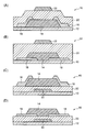
- FIG. 1A and 1B are diagrams showing a thin film transistor of an embodiment, in which FIG. 1A is a top gate-top contact type, FIG. 1B is a top gate-bottom contact type, FIG. 3C is a bottom gate-top contact type, and FIG. -A cross-sectional view schematically showing a configuration of a bottom contact type thin film transistor.
- FIG. -A cross-sectional view schematically showing a configuration of a bottom contact type thin film transistor.
- FIG. 9A is a plan view of the TFT of Experimental Example 2
- FIG. 9B is a cross-sectional view taken along the line AA of the TFT shown in FIG. 9A.
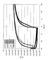
- FIG. 6 is a diagram showing Vg-Id characteristics in Experimental Example 2.
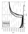
- FIG. 6 is a diagram showing Vg-Id characteristics in Experimental Examples 22 to 24 (annealing temperature 150 ° C.).
- FIG. 6 is a diagram showing Vg-Id characteristics in Experimental Examples 25 to 27 (annealing temperature 200 ° C.).
- FIG. 6 is a diagram showing Vg-Id characteristics in Experimental Examples 28 to 30 (annealing temperature 250 ° C.).
- a thin film transistor (hereinafter abbreviated as TFT) according to an embodiment of the present invention includes a gate electrode, a gate insulating film, an active layer, a source electrode, and a drain electrode, and applies a voltage to the gate electrode to cause a current flowing in the active layer. And an active element having a function of switching current between the source electrode and the drain electrode.
- the element structure of the TFT may be any of a so-called inverted stagger structure (also referred to as a bottom gate type) and a stagger structure (also referred to as a top gate type) based on the position of the gate electrode. Further, based on the contact portion between the active layer and the source and drain electrodes (referred to as “source / drain electrodes” as appropriate), either a so-called top contact type or bottom contact type may be used.
- the top gate type is a form in which a gate electrode is disposed on the upper side of the gate insulating film and an active layer is formed on the lower side of the gate insulating film.
- the bottom gate type is a type on the lower side of the gate insulating film.
- a gate electrode is disposed and an active layer is formed above the gate insulating film.
- the bottom contact type is a mode in which the source / drain electrodes are formed before the active layer and the lower surface of the active layer is in contact with the source / drain electrodes.
- the top contact type is the type in which the active layer is the source / drain. In this embodiment, the upper surface of the active layer is in contact with the source / drain electrodes.
- FIG. 1A is a schematic diagram showing an example of a top contact type TFT having a top gate structure, which is a TFT according to an embodiment of the present invention.
- an active layer 14 is stacked on one main surface of a substrate 12.
- a source electrode 16 and a drain electrode 18 are disposed on the active layer 14 so as to be spaced apart from each other, and a gate insulating film 20 and a gate electrode 22 are sequentially stacked thereon.
- FIG. 1B is a schematic view showing an example of a bottom contact type TFT having a top gate structure, which is a TFT according to an embodiment of the present invention.
- the source electrode 16 and the drain electrode 18 are provided on one main surface of the substrate 12 so as to be separated from each other.
- the active layer 14, the gate insulating film 20, and the gate electrode 22 are sequentially stacked.
- FIG. 1C is a schematic diagram showing an example of a top contact type TFT having a bottom gate structure, which is a TFT according to an embodiment of the present invention.
- the gate electrode 22, the gate insulating film 20, and the active layer 14 are sequentially stacked on one main surface of the substrate 12.
- a source electrode 16 and a drain electrode 18 are spaced apart from each other on the surface of the active layer 14.
- FIG. 1D is a schematic view showing an example of a bottom contact type TFT with a bottom gate structure, which is a TFT according to an embodiment of the present invention.
- the gate electrode 22 and the gate insulating film 20 are sequentially stacked on one main surface of the substrate 12.
- a source electrode 16 and a drain electrode 18 are disposed on the surface of the gate insulating film 20 so as to be spaced apart from each other, and an active layer 14 is further stacked thereon.
- the TFT according to the present embodiment can have various configurations other than the above, and may appropriately have a configuration including a protective layer on the active layer, an insulating layer on the substrate, and the like.
- top contact type TFT 10 with the top gate structure shown in FIG. 1A will be specifically described.
- present invention is similarly applied to the case of manufacturing other types of TFTs. can do.
- the structure of the substrate 12 may be a single layer structure or a laminated structure.
- a substrate made of an inorganic material such as glass or YSZ (yttrium stabilized zirconium), a resin, a resin composite material, or the like can be used as the substrate 12, for example.
- a substrate made of a resin or a resin composite material is preferable in terms of light weight and flexibility.
- at least one contact Insulating the surface by subjecting a substrate made of a composite material having a barrier property having an interface, a stainless steel substrate, a metal multilayer substrate in which stainless steel and a dissimilar metal are laminated, an aluminum substrate or a surface to an oxidation treatment (for example, anodization treatment).
- An aluminum substrate with an improved oxide film can be used.
- the resin substrate is preferably excellent in heat resistance, dimensional stability, solvent resistance, electrical insulation, workability, low air permeability, low moisture absorption, and the like.
- the resin substrate may include a gas barrier layer for preventing permeation of moisture and oxygen, an undercoat layer for improving the flatness of the resin substrate and adhesion with the lower electrode, and the like.
- the thickness of the substrate is preferably 50 ⁇ m or more and 500 ⁇ m or less.
- the thickness of the substrate is 50 ⁇ m or more, the flatness of the substrate itself is further improved.
- the thickness of the substrate is 500 ⁇ m or less, the flexibility of the substrate itself is further improved, and the use as a substrate for a flexible device becomes easier.
- the thickness which has sufficient flatness and flexibility changes with materials which comprise the board
- the active layer 14 contains an oxide semiconductor composed of at least two elements of In, Ga, and Zn and O as a main component.
- the “main component” represents a component that is contained in the largest amount among the constituent components constituting the active layer 14.
- the active layer (mainly oxide semiconductor) may be either amorphous or crystalline, but is preferably amorphous. Whether the active layer is crystalline or amorphous can be confirmed by X-ray diffraction measurement. That is, when a clear peak indicating a crystal structure is not detected by X-ray diffraction measurement, it can be determined that the active layer is amorphous. If the active layer is amorphous, it can be formed at a low temperature of less than 300 ° C., so that it can be easily formed on a flexible resin substrate such as a plastic substrate. Therefore, application to a flexible display using a plastic substrate with TFT becomes easier. Furthermore, an amorphous film is easy to form a uniform film over a large area, and since there is no grain boundary like a polycrystal, it is easy to suppress variations in device characteristics.
- the active layer 14 may have a composition distribution in the layer thickness direction or a plane direction perpendicular to the layer thickness direction. Similarly, the active layer 14 has an oxygen concentration distribution in the layer thickness direction and the plane direction perpendicular to the layer thickness direction. You may have.
- the resistivity of the active layer 14 may be a resistivity that generally behaves as a semiconductor.
- the resistivity at room temperature (20 ° C.) is 1 ⁇ cm or more and 1 ⁇ 10 6 ⁇ cm. It is preferable that:
- the resistivity of this embodiment is the value measured by ResiTest8310 (made by Toyo Technica Co., Ltd.).
- the film thickness (total film thickness) of the active layer 14 is not particularly limited, but is preferably 10 nm or more and 200 nm or less.
- the optical band gap of the IGZO film is relatively narrow.
- the band gap of the material used for the active layer 14 is larger than 3.0 eV, particularly for a TFT used for driving an organic EL.
- the number of H 2 O molecules observed by temperature programmed desorption gas analysis is preferably 4.2 ⁇ 10 20 cm ⁇ 3 or less.
- the active layer 14 in which the number of H 2 O molecules observed by thermal desorption gas analysis is 4.2 ⁇ 10 20 cm ⁇ 3 or less is an oxidation in which moisture that induces surplus carriers contained in the film is eliminated. It is a thin semiconductor film and exhibits good semiconductor characteristics.
- the source electrode 16 and the drain electrode 18 are not particularly limited as long as they have high conductivity (for example, higher than that of the active layer 14).
- metals such as Al, Mo, Cr, Ta, Ti, Au, and Ag
- a metal oxide conductive film such as Al—Nd, tin oxide, zinc oxide, indium oxide, indium tin oxide (ITO), and indium zinc oxide (IZO) can be used as a single layer or a stacked structure of two or more layers. it can.
- the thickness is preferably 10 nm or more and 1000 nm or less in consideration of the film forming property, the patterning property by etching or lift-off method, and the conductivity. 50 nm or more and 100 nm or less is more preferable.
- the gate insulating film 20 is preferably one having high insulating properties, for example, an insulating film such as SiO 2 , SiN x , SiON, Al 2 O 3 , Y 2 O 3 , Ta 2 O 5 , HfO 2 , or the like. It can be composed of an insulating film containing at least two compounds. Note that the gate insulating film 20 needs to have a sufficient thickness in order to reduce the leakage current and improve the voltage resistance. On the other hand, if the thickness is too large, the driving voltage increases. Although depending on the material, the thickness of the gate insulating film 20 is preferably 10 nm to 10 ⁇ m, more preferably 50 nm to 1000 nm, and particularly preferably 100 nm to 400 nm.
- the gate electrode 22 is not particularly limited as long as it has high conductivity.
- a metal such as Al, Mo, Cr, Ta, Ti, Au, and Ag, Al—Nd, tin oxide, zinc oxide, indium oxide,
- a metal oxide conductive film such as indium tin oxide (ITO) or zinc indium oxide (IZO) can be used as a single layer or a stacked structure of two or more layers.
- the thickness thereof is preferably 10 nm or more and 1000 nm or less, taking into consideration the film forming property, patterning property by etching or lift-off method, conductivity, etc., 50 nm or more, More preferably, it is 200 nm or less.
- TFT manufacturing method> a method for manufacturing a TFT according to an embodiment of the present invention will be described.
- a top contact type TFT 10 with the top gate structure shown in FIG. 1A will be specifically described.
- the present invention is similarly applied to the case of manufacturing other types of TFTs. can do.
- a method for manufacturing a TFT according to an embodiment of the present invention includes: A film forming step of forming an active layer 14 containing, as a main component, an oxide semiconductor composed of at least two elements of In, Ga, and Zn and O in a film formation chamber into which at least oxygen is introduced, and drying A heat treatment step of heat-treating the active layer 14 at a temperature lower than 300 ° C. under an atmosphere,
- the oxygen partial pressure with respect to the total pressure of the atmosphere in the film forming chamber in the film forming step is Po 2 depo (%)
- the oxygen partial pressure with respect to the total pressure of the atmosphere in the heat treatment step is Po 2 anneal (%).
- a substrate 12 made of any one of the materials described above is prepared, and the substrate 12 is placed in a film formation chamber. After introducing at least oxygen into the deposition chamber, an oxide semiconductor composed of at least two elements of In, Ga, and Zn and O is formed on one main surface of the substrate 12 in the deposition chamber. A film forming step for forming the active layer 14 containing as a main component is performed.
- the oxide semiconductor of the active layer 14 is preferably composed of In, Ga, Zn, and O (IGZO).
- IGZO In, Ga, Zn, and O
- the molar ratio of Ga to the sum of the molar ratio of In and the molar ratio of Ga satisfies the relationship of 0.375 ⁇ Ga / (In + Ga) ⁇ 0.9. If it is in the above composition range, a normally-off driving TFT can be reliably obtained. More preferably, the molar ratio of Ga to the sum of the molar ratio of In and the molar ratio of Ga is 0.375 ⁇ Ga / (In + Ga) ⁇ 0.625.
- TFT which shows favorable field effect mobility, for example, 10 cm ⁇ 2 > / Vs or more will be obtained. Furthermore, a deeper well-type potential structure can be obtained by doping part of Zn of the oxide semiconductor with element ions having a wider band gap. Specifically, the band gap of the film can be increased by doping Mg.
- the film formation method of the active layer 14 is, for example, a vacuum film formation chamber in which the amount of introduced oxygen can be adjusted, such as a physical method such as vacuum deposition, sputtering, or ion plating, or a chemical method such as CVD or plasma CVD.
- a physical method such as vacuum deposition, sputtering, or ion plating
- CVD chemical method
- CVD plasma CVD
- the carrier density of the active layer 14 is arbitrarily controlled by controlling the amount of oxygen vacancies or cation doping.
- the amount of oxygen vacancies may be increased, or a material (for example, Ti, Zr, Hf, Ta, etc.) that easily becomes a cation having a relatively large valence may be doped.
- a material for example, Ti, Zr, Hf, Ta, etc.
- the oxygen partial pressure Po 2 depo (%) in the film forming chamber during the film forming process is such that the oxygen partial pressure Po 2 anneal (%) in the heat treatment step is ⁇ 20/3 Po 2 depo + 40/3 ⁇ Po 2 anneal. ⁇ ⁇ 800 / 43 Po 2 depo + 5900/43 is appropriately adjusted.
- the oxygen partial pressure Po 2 depo is decreased to increase the amount of oxygen vacancies.
- the mobility increases as the carrier density increases. The behavior to do is reported.
- excessive oxygen deficiency simultaneously becomes a scatterer for carriers, and conversely causes a decrease in mobility. Therefore, it is preferable to adjust the oxygen partial pressure Po 2 depo to 0.17% or more.
- the oxygen partial pressure Po 2 depo it is preferable to adjust the oxygen partial pressure Po 2 depo to 0.50% or more.
- the oxygen partial pressure is 0.50% or more, carrier scattering due to excessive oxygen vacancies as described above is small, and a TFT with high mobility and normally-off driving is easily obtained.
- the oxygen partial pressure Po 2 depo is not more than 6.3%.
- the oxygen partial pressure Po 2 depo exceeds 6.3%, the oxygen vacancy density in the active layer before the heat treatment is relatively low, and although it is a normally-off driving TFT, This is because the reduction tends to cause a decrease in mobility.
- the atmosphere during film formation is not particularly limited as long as it contains oxygen.
- it may contain argon or nitrogen in addition.
- the film formation temperature of the active layer 14 is preferably a low temperature of less than 300 ° C. from the viewpoint of enhancing the selectivity of the substrate 12, and is preferably 200 ° C. or less, for example, from the viewpoint of making it amorphous. From the viewpoint of omitting, it is more preferable that the temperature is normal temperature (25 ° C.).
- the active layer 14 is appropriately patterned. Patterning can be performed by photolithography and etching. Specifically, a resist pattern is formed on the remaining portion by photolithography, and the pattern is formed by etching with an acid solution such as hydrochloric acid, nitric acid, dilute sulfuric acid, or a mixed solution of phosphoric acid, nitric acid and acetic acid.
- an acid solution such as hydrochloric acid, nitric acid, dilute sulfuric acid, or a mixed solution of phosphoric acid, nitric acid and acetic acid.
- a process of controlling the oxygen vacancy density in the active layer 14 by irradiating the film-forming surface of the active layer 14 with oxygen-containing radicals during the formation of the active layer 14 and / or after the active layer 14 is formed. It may be included. Further, during the formation of the active layer 14 and / or after the formation of the active layer 14, the surface of the active layer 14 is irradiated with ultraviolet rays in an ozone atmosphere to control the oxygen vacancy density in the active layer 14. The process to perform may be included.
- a heat treatment process is performed in which the active layer 14 is heat-treated at a temperature lower than 300 ° C. in a dry atmosphere.
- the active layer 14 may be after any step as long as it is after the active layer 14 is formed, for example, immediately after the formation of the active layer 14 or after the electrode formation described later, or the TFT array is completed. After you do.
- the reason for the dry atmosphere is to realize a normally-off driving TFT.
- the dry atmosphere means that the moisture content contained in the entire atmosphere is ⁇ 36 ° C. or less in terms of dew point temperature (absolute humidity 0.21 g / m ⁇ 3 or less), and the atmosphere contains almost no moisture. To do.
- the reason why the temperature is lower than 300 ° C. is to increase the selectivity of the substrate.
- the oxygen partial pressure Po 2 anneal during the heat treatment is adjusted so as to satisfy the relationship -20 / 3Po 2 depo + 40/ 3 ⁇ Po 2 anneal ⁇ -800 / 43Po 2 depo + 5900/43 .
- a TFT with high field effect mobility and normally-off driving can be realized.
- the heat treatment temperature during the heat treatment step is preferably higher than 150 ° C. from the viewpoint of reliably obtaining a normally-off driving TFT. Furthermore, the heat treatment temperature is preferably 250 ° C. or lower from the viewpoint of increasing mobility. Furthermore, the heat treatment temperature is preferably 200 ° C. or lower. By selecting a low temperature region of 200 ° C. or lower, the selectivity of the substrate 12 to which the heat treatment can be applied is greatly increased, and the heat treatment can be easily applied to a TFT formed on a flexible substrate such as plastic.
- the atmosphere at the time of heat processing may contain oxygen, it may contain argon and nitrogen.
- a conductive film for forming the source / drain electrodes 16 and 18 is formed on the active layer 14 after the film formation step of the active layer 14 or the heat treatment step. Next, the conductive film is patterned into a predetermined shape by etching or a lift-off method to form the source electrode 16 and the drain electrode 18. At this time, it is preferable to pattern the source / drain electrodes 16 and 18 and wiring (not shown) connected to these electrodes simultaneously.
- the conductive film of the source electrode 16 and the drain electrode 18 may be formed by a wet method such as a printing method or a coating method, a physical method such as a vacuum deposition method, a sputtering method, or an ion plating method, a CVD method, or a plasma CVD method.
- the film may be formed according to a method appropriately selected in consideration of suitability with a material to be used from among chemical methods such as the above.
- the gate insulating film 20 is formed.
- the gate insulating film 20 is patterned into a predetermined shape by photolithography and etching.
- the gate insulating film 20 is formed by a wet method such as a printing method or a coating method, a physical method such as a vacuum deposition method, a sputtering method, or an ion plating method, or a chemical method such as CVD or plasma CVD method.
- the film may be formed according to a method appropriately selected in consideration of suitability with the material to be used.
- a gate electrode 22 is formed. After the electrode film is formed, it is patterned into a predetermined shape by etching or a lift-off method to form the gate electrode 22. At this time, it is preferable to pattern the gate electrode 22 and the gate wiring simultaneously.
- the gate electrode 22 is formed by a wet method such as a printing method or a coating method, a physical method such as a vacuum deposition method, a sputtering method or an ion plating method, or a chemical method such as a CVD or plasma CVD method.
- the film may be formed according to a method appropriately selected in consideration of suitability with the material to be used.
- the TFT 10 illustrated in FIG. 1A can be manufactured.
- a TFT exhibiting normally-off characteristics with a field-effect mobility exceeding 10 cm 2 / Vs can be obtained.
- the application of the TFT of the present embodiment described above is not particularly limited.
- an electro-optical device for example, a liquid crystal display device, an organic EL (Electro Luminescence) display device, a display device such as an inorganic EL display device, etc.
- driving elements particularly large area devices.
- the TFT of the embodiment is particularly suitable for a device that can be manufactured by a low-temperature process using a resin substrate (for example, a flexible display), and various sensors such as an X-ray sensor, MEMS (Micro Electro Mechanical System), and the like. It is preferably used as a drive element (drive circuit) in an electronic device.
- the electro-optical device or sensor according to this embodiment includes the above-described thin film transistor of the present invention.
- electro-optical devices include display devices (eg, liquid crystal display devices, organic EL display devices, inorganic EL display devices, etc.).
- an image sensor such as a CCD (Charge Coupled Device) or a CMOS (Complementary Metal Oxide Semiconductor), an X-ray sensor, or the like is suitable.
- Both the electro-optical device and the sensor using the TFT of this embodiment have high in-plane uniformity of characteristics.
- the “characteristic” referred to here is a display characteristic in the case of an electro-optical device (display device), and a sensitivity characteristic in the case of a sensor.
- a liquid crystal display device, an organic EL display device, and an X-ray sensor will be described as representative examples of the electro-optical device or sensor including the thin film transistor manufactured according to the present embodiment.
- FIG. 2 is a schematic sectional view of a part of a liquid crystal display device according to an embodiment of the electro-optical device of the present invention
- FIG. 3 is a schematic configuration diagram of the electric wiring.
- the liquid crystal display device 100 of this embodiment has a top gate structure 10 shown in FIG. 1A and a top contact type TFT 10 and a gate electrode 22 protected by a passivation layer 102 of the TFT 10.
- a liquid crystal layer 108 sandwiched between the pixel lower electrode 104 and the counter upper electrode 106, and an RGB color filter 110 for developing different colors corresponding to each pixel, and the substrate 12 side of the TFT 10 and the RGB color filter 110 are provided. It is the structure provided with polarizing plates 112a and 112b, respectively.
- the liquid crystal display device 100 of the present embodiment includes a plurality of gate lines 112 parallel to each other and data lines 114 parallel to each other intersecting the gate lines 112.
- the gate wiring 112 and the data wiring 114 are electrically insulated.
- the TFT 10 is provided in the vicinity of the intersection between the gate wiring 112 and the data wiring 114.
- the gate electrode 22 of the TFT 10 is connected to the gate wiring 112, and the source electrode 16 of the TFT 10 is connected to the data wiring 114.
- the drain electrode 18 of the TFT 10 is connected to the pixel lower electrode 104 through a contact hole 116 provided in the gate insulating film 20 (a conductor is embedded in the contact hole 116).
- the pixel lower electrode 104 forms a capacitor 118 together with the grounded counter upper electrode 106.
- the TFT 10 having the top gate structure is provided in the liquid crystal display device of this embodiment shown in FIG. 2.
- the TFT used in the liquid crystal display device which is the display device of the present invention is limited to the top gate structure.
- a bottom gate TFT may be used.
- the TFT 10 since the TFT 10 according to the embodiment of the present invention has high mobility, high-definition display such as high definition, high-speed response, and high contrast can be performed on the liquid crystal display device 100, which is suitable for a large screen.
- the active layer IGZO when the active layer IGZO is amorphous, variations in device characteristics can be suppressed, and an excellent display quality with a large screen and no unevenness can be realized.
- the gate voltage can be reduced, and thus the power consumption of the display device can be reduced.
- the thin film transistor can be manufactured using an amorphous IGZO film that can be formed at a low temperature (for example, 300 ° C. or less) as the active layer 14, a resin substrate (plastic) is used as the substrate 12. Substrate). Therefore, a flexible liquid crystal display device having excellent display quality can be provided.
- FIG. 4 shows a schematic sectional view of a part of an active matrix organic EL display device according to an embodiment of the electro-optical device of the present invention
- FIG. 5 shows a schematic configuration diagram of electric wiring.
- the simple matrix method has an advantage that it can be manufactured at low cost.
- the number of scanning lines and the light emission time per scanning line are inversely proportional. Therefore, it is difficult to increase the definition and increase the screen size.
- the active matrix method has a high manufacturing cost because a transistor and a capacitor are formed for each pixel.
- it is suitable for high definition and large screen.
- the top gate TFT 10 shown in FIG. 1A is provided as a driving TFT 204 and a switching TFT 206 on a substrate 12 having a passivation layer 202.
- an organic EL light emitting element 214 composed of an organic light emitting layer 212 sandwiched between the lower electrode 208 and the upper electrode 210 is provided on the TFTs 204 and 206, and the upper surface is also protected by the passivation layer 216.
- the organic EL display device 200 includes a plurality of gate wirings 220 that are parallel to each other, and a data wiring 222 and a driving wiring 224 that are parallel to each other and intersect the gate wiring 220.
- the gate wiring 220, the data wiring 222, and the drive wiring 224 are electrically insulated.
- the gate electrode 22 of the switching TFT 10 b is connected to the gate wiring 220, and the source electrode 16 of the switching TFT 10 b is connected to the data wiring 222.
- the drain electrode 18 of the switching TFT 10b is connected to the gate electrode 22 of the driving TFT 10, and the driving TFT 10a is kept on by using the capacitor 226.
- the source electrode 16 of the driving TFT 10 a is connected to the driving wiring 224, and the drain electrode 18 is connected to the organic EL light emitting element 214.
- the organic EL device of this embodiment shown in FIG. 4 includes the top gate TFTs 10a and 10b.
- the TFT used in the organic EL device which is the display device of the present invention is limited to the top gate structure.
- a TFT having a bottom gate structure may be used.
- a thin film transistor can be manufactured using an amorphous IGZO film that can be formed at a low temperature (for example, 300 ° C. or less) as the active layer 14, and thus the resin substrate as the substrate 12. (Plastic substrate) can be used. Therefore, a flexible organic EL display device having excellent display quality can be provided.
- the top electrode 210 may be a top emission type using a transparent electrode, or the bottom electrode 208 and each electrode of a TFT may be a transparent electrode.
- FIG. 6 shows a schematic sectional view of a part of an X-ray sensor which is an embodiment of the sensor of the present invention
- FIG. 7 shows a schematic configuration diagram of its electric wiring.
- FIG. 6 is a schematic cross-sectional view in which a part of the X-ray sensor array is enlarged more specifically.
- the X-ray sensor 300 of this embodiment includes the TFT 10 and the capacitor 310 formed on the substrate 12, the charge collection electrode 302 formed on the capacitor 310, the X-ray conversion layer 304, and the upper electrode 306. Composed.
- a passivation film 308 is provided on the TFT 10.
- the capacitor 310 has a structure in which an insulating film 316 is sandwiched between a capacitor lower electrode 312 and a capacitor upper electrode 314.
- the capacitor upper electrode 314 is connected to one of the source electrode 16 and the drain electrode 18 (the drain electrode 18 in FIG. 6) of the TFT 10 through a contact hole 318 provided in the insulating film 316.
- the charge collection electrode 302 is provided on the capacitor upper electrode 314 in the capacitor 310 and is in contact with the capacitor upper electrode 314.
- the X-ray conversion layer 304 is a layer made of amorphous selenium, and is provided so as to cover the TFT 10 and the capacitor 310.
- the upper electrode 306 is provided on the X-ray conversion layer 304 and is in contact with the X-ray conversion layer 304.
- the X-ray sensor 300 of this embodiment includes a plurality of gate wirings 320 that are parallel to each other and a plurality of data wirings 322 that intersect with the gate wirings 320 and are parallel to each other.
- the gate wiring 320 and the data wiring 322 are electrically insulated.
- the TFT 10 is provided in the vicinity of the intersection between the gate wiring 320 and the data wiring 322.
- the gate electrode 22 of the TFT 10 is connected to the gate wiring 320, and the source electrode 16 of the TFT 10 is connected to the data wiring 322.
- the drain electrode 18 of the TFT 10 is connected to the charge collecting electrode 302, and the charge collecting electrode 302 is connected to the capacitor 310.
- X-rays are irradiated from the upper part (upper electrode 306 side) in FIG. 6, and electron-hole pairs are generated in the X-ray conversion layer 304.
- the generated charge is accumulated in the capacitor 310 and read out by sequentially scanning the TFT 10.
- the X-ray sensor 300 since the X-ray sensor 300 according to this embodiment of the present invention includes the TFT 10 having a high on-current and excellent reliability, the S / N is high and the sensitivity characteristic is excellent, so that the X-ray sensor 300 is used for an X-ray digital imaging apparatus. A wide dynamic range image can be obtained.
- the X-ray digital imaging apparatus according to the present embodiment of the present invention is not only capable of taking still images, but is preferably used for an X-ray digital imaging apparatus that can perform fluoroscopy and still image shooting with a single camera. is there. Furthermore, when the IGZO of the active layer 14 in the TFT is amorphous, an image with excellent uniformity can be obtained.
- the X-ray sensor of this embodiment shown in FIG. 6 is provided with a TFT having a top gate structure, but the TFT used in the sensor of the present invention is not limited to the top gate structure.
- a TFT having a structure may be used.
- the present inventors Perform the following experiment to confirm that good semiconductor characteristics can be obtained in a specific range of conditions for heat treatment below 300 ° C by changing the oxygen partial pressure, the atmosphere during heat treatment performed after the film formation process, and the temperature of the heat treatment. did.
- Example 1 As Experimental Example 1, an oxide semiconductor thin film made of IGZO that can be applied as an active layer was formed to a thickness of 100 nm on a non-doped Si substrate (manufactured by Mitsubishi Materials Corporation) by a sputtering method.
- the sputtering conditions for the oxide semiconductor thin film are as follows.
- An oxide semiconductor thin film that was heat-treated at 200 ° C. in the atmosphere described above was manufactured.
- the atmosphere in the heat treatment is that argon and oxygen are supplied from a gas cylinder, which does not substantially contain water vapor, and the moisture content contained in the whole atmosphere is ⁇ 36 ° C. or less in terms of dew point temperature (absolute humidity 0.21 g / m ⁇ 3 or less) corresponding to a heat treatment in a dry atmosphere (referred to as dry annealing).
- Comparative Example 1 As Comparative Example 1, an oxide semiconductor thin film was produced in the same manner as in Experimental Example 1 except for the heat treatment conditions. Specifically, an oxide semiconductor thin film is formed by the same method as in Experimental Example 1, and then the oxide semiconductor thin film is formed in the atmosphere at a temperature of 23 ° C. and a humidity of 66% (the moisture content contained in the entire atmosphere is A heat treatment (referred to as wet annealing) at 200 ° C. was performed at a dew point temperature conversion of 16 ° C. (absolute humidity 13.6 g / m ⁇ 3 )).
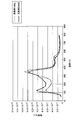
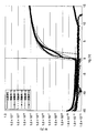
- FIG. 8 is a graph showing the results of thermal desorption gas analysis.
- the intensity peak observed at 100 ° C. to 200 ° C. corresponding to the desorption of H 2 O is a comparative example in which the oxide semiconductor thin film of Experimental Example 1 subjected to dry annealing is wet annealed. It was found that it was reduced to about 65% (2/3) compared to 1. That is, it was found that the oxide semiconductor thin film of Experimental Example 1 had a lower moisture content in the film.
- FIG. 9A is a plan view of the TFT of Experimental Example 2, and FIG. 9B is a cross-sectional view taken along the line AA of the TFT shown in FIG. 9A.
- the TFT 500 of Experimental Example 2 was specifically manufactured as follows.
- the substrate 502 a heavily doped p-type silicon substrate (manufactured by Mitsubishi Materials Corporation) on which a 100 nm SiO 2 oxide film 504 was formed was used.
- the IGZO layer was formed by a co-sputter method using an In 2 O 3 target, a Ga 2 O 3 target, and a ZnO target.
- the detailed sputtering conditions of the IGZO layer are the same as the conditions of the oxide semiconductor thin film of Experimental Example 1.
- Experimental Example 2 is a thin film transistor in which an active layer includes an oxide semiconductor thin film containing 4.2 ⁇ 10 20 cm ⁇ 3 H 2 O molecules in the film, as in Experimental Example 1.
- Comparative Example 2 As the TFT of Comparative Example 2, heat treatment was performed in the atmosphere (humidity 66%), and everything else was prepared by the same method. That is, Comparative Example 2 is a TFT having an active layer including an oxide semiconductor thin film containing 4.4 ⁇ 10 20 cm ⁇ 3 H 2 O molecules in the film, as in Comparative Example 1.
- Table 3 shows the threshold voltage (Vth) and field effect mobility of the TFTs of Experimental Example 2 and Comparative Example 2 calculated from the measurement results.
- W is the channel width of the active layer
- L is the channel length of the active layer
- C is the capacitance per unit area of the gate insulating film
- Vgs is the voltage applied between the gate and source electrodes
- ⁇ sat is the saturation mobility It is.
- a normally-off driving TFT is more preferable than a normally-on driving
- the experimental example 1 is a TFT exhibiting more preferable semiconductor characteristics. I understood.
- FIGS. 11A to 11C show Vg-Id characteristics measured in Experimental Examples 3 to 20 and Comparative Examples 3 to 5.
- FIGS. Table 4 shows a summary of the oxygen partial pressure during the heat treatment and the oxygen partial pressure conditions during the formation of the active layer, the sample name, the threshold voltage, and the field effect mobility.
- FIGS. 11A to 11C and Table 4 indicate that a normally-off driving element is obtained in a wide range of oxygen partial pressures, indicating that the characteristic control method has a wide process margin.
- a normally-off drive element was obtained even when the heat treatment atmosphere did not contain oxygen. This means that heat treatment in a dry atmosphere is essentially effective in low temperature processes.
- FIG. 12 is a diagram showing the relationship between the oxygen partial pressure during the formation of the active layer and the oxygen partial pressure during the heat treatment.
- ⁇ in the figure is an example
- x is a comparative example It becomes.
- the oxygen partial pressure with respect to the total pressure of the atmosphere in the film forming chamber in the film forming step is Po 2 depo (%)
- the oxygen partial pressure with respect to the total pressure of the atmosphere in the heat treatment step is Po 2 anneal.
- the oxygen partial pressure Po 2 anneal during heat treatment step (%) is represented in the range of -20 / 3Po 2 depo + 40/ 3 ⁇ Po 2 anneal ⁇ -800 / 43Po 2 depo + 5900/43 I understood that.
- the oxygen partial pressure Po 2 depo (%) during film formation is 0.50% or more, the oxygen partial pressure conditions for obtaining normally-off driving are sufficiently wide, which is preferable from the viewpoint of process margin.
- the oxygen partial pressure Po 2 depo (%) at the time of forming the active layer is 6.3%, normally-off driving is obtained, but when the oxygen partial pressure during annealing is 100%, the mobility is high. It was found to reduce. Therefore, the oxygen partial pressure Po 2 depo (%) during the formation of the active layer is more preferably 6.3% or less.
- the lower limit value of the oxygen partial pressure Po 2 depo (%) at the time of forming the active layer was determined by measuring the hole mobility of the IGZO film.
- the oxygen partial pressure during film formation is preferably 0.17% or more, and from the viewpoint of carrier concentration control and mobility, the oxygen partial pressure during film formation is more preferably 0.50% or more.
- FIGS. 13A to 13C The results of measuring the Vg-Id characteristics in these Experimental Examples 22 to 30 (31 is omitted) are shown in FIGS. 13A to 13C.
- Table 6 shows a summary of the temperature during heat treatment, the condition of oxygen partial pressure during heat treatment, the sample name, the threshold voltage, and the mobility.
Landscapes
- Chemical & Material Sciences (AREA)
- Engineering & Computer Science (AREA)
- Materials Engineering (AREA)
- Chemical Kinetics & Catalysis (AREA)
- Mechanical Engineering (AREA)
- Metallurgy (AREA)
- Organic Chemistry (AREA)
- Physics & Mathematics (AREA)
- Thermal Sciences (AREA)
- Nonlinear Science (AREA)
- Mathematical Physics (AREA)
- Crystallography & Structural Chemistry (AREA)
- Microelectronics & Electronic Packaging (AREA)
- General Physics & Mathematics (AREA)
- Optics & Photonics (AREA)
- Thin Film Transistor (AREA)
- Liquid Crystal (AREA)
- Physical Deposition Of Substances That Are Components Of Semiconductor Devices (AREA)
- Solid State Image Pick-Up Elements (AREA)
- Formation Of Insulating Films (AREA)
- Nanotechnology (AREA)
- Health & Medical Sciences (AREA)
- Toxicology (AREA)
Abstract
基板の選択性を広げつつ、電界効果移動度が高くノーマリーオフ駆動する薄膜トランジスタ等を得る。活性層の成膜工程での成膜室中の雰囲気の全圧に対する酸素分圧をPo2depo(%)とし、熱処理工程中の雰囲気の全圧に対する酸素分圧をPo2anneal(%)としたときに、熱処理工程時の酸素分圧Po2anneal(%)が、-20/3Po2depo+40/3≦Po2anneal≦-800/43Po2depo+5900/43の関係を満たすように成膜工程と熱処理工程とを行う。
Description
本発明は、薄膜トランジスタの製造方法、薄膜トランジスタ、表示装置、センサ及びX線デジタル撮影装置に関する。
近年、In-Ga-Zn-O系(以下、IGZOと称す)の酸化物半導体薄膜を活性層(チャネル層)に用いた薄膜トランジスタの研究開発が盛んである。酸化物半導体薄膜は低温成膜が可能であり、且つアモルファスシリコンよりも高移動度を示し、更に可視光に透明であることから、プラスチック板やフィルム等の基板上にフレキシブルな薄膜トランジスタを形成することが可能である。
ここで、表1に各種トランジスタ特性の電界効果移動度やプロセス温度等の比較表を示す。

表1に示すように、活性層がポリシリコンの薄膜トランジスタは100cm2/Vs程度の移動度を得ることが可能だが、プロセス温度が450℃以上と非常に高いために、耐熱性が高い基板にしか形成できず、安価、大面積、フレキシブル化には不向きである。また、活性層がアモルファスシリコンの薄膜トランジスタは300℃程度の比較的低温で形成可能なため、基板の選択性はポリシリコンに比べて広いが、せいぜい1cm2/Vs程度の移動度しか得られず高精細なディスプレイ用途には不向きである。一方、低温成膜という観点では活性層が有機物の薄膜トランジスタは100℃以下での形成が可能なため、耐熱性の低いプラスティックフィルム基板等を用いたフレキシブルディスプレイ用途等への応用が期待されているが、移動度はアモルファスシリコンと同程度の結果しか得られていない。
製造プロセスにおいて、トランジスタの電気特性を向上させるために素子形成後に熱処理(ポストアニール処理)を行うことがしばしば見られる。酸化物半導体薄膜を活性層に用いた薄膜トランジスタにおいては、上述の通り低温形成によっても高移動度・高信頼性を示すデバイスを形成可能であり、熱処理時の温度を、低減させることが期待されている。
IGZO系の酸化物半導体薄膜を活性層に用いた薄膜トランジスタにおいて、熱処理によって所望の電気特性に制御する手法が幾つか報告されている。
特開2008-53356号公報には、活性層がIGZO系の薄膜トランジスタにおいて、活性層形成後に250℃~450℃の温度範囲で熱処理を行うことが記載されている。また、酸素ラジカル、オゾンを照射しながら150℃~450℃の温度範囲で熱処理を行うことも記載されている。
特開2010-238770号公報には、活性層がIGZO系の薄膜トランジスタにおいて、活性層形成後に200℃~500℃の温度範囲で熱処理を行うことが記載されている。そして、この方法の一例として、特開2010-238770号の実施例3では、酸素濃度を1%としたアルゴンと酸素の混合ガス雰囲気下でIGZOからなる活性層を成膜し、その後に、100%の雰囲気中300℃で熱処理を行うことが記載されている。
しかしながら、特開2008-53356号、特開2010-238770号において、300℃以上の高温で熱処理する場合、耐熱性の観点から、プラスチック基板などのフレキシブル基板上に形成したトランジスタには用いる事が困難であるという問題点がある。また、300℃未満の低温で熱処理する場合、低抵抗化が起こり得るため、単に熱処理温度を調整しただけでは、ノーマリーオフ駆動のトランジスタを得ることは困難である。さらに、300℃未満の低温で熱処理する場合、電界効果移動度が、例えば7.1cm2/Vs程度(特開2010-238770号の実験例3参照)となり、10cm2/Vs以上となっていない。さらにまた、特開2008-53356号のように、酸素ラジカル、オゾンを照射しながら熱処理を行う場合、150℃~450℃の温度範囲で高安定性が得られるが、プロセスが複雑化する。
本発明は上記事実に鑑みてなされたものであり、基板の選択性を広げつつ、電界効果移動度が高くノーマリーオフ駆動する薄膜トランジスタの製造方法、薄膜トランジスタ、表示装置、センサ及びX線デジタル撮影装置を提供することを目的とする。
本発明の上記課題は下記の手段によって解決された。
<1>In,Ga及びZnのうち少なくとも2種類の元素とOで構成される酸化物半導体を主成分として含有する活性層を、少なくとも酸素を導入した成膜室内で成膜する成膜工程と、乾燥雰囲気下において前記活性層を300℃未満で熱処理する熱処理工程と、を有する薄膜トランジスタの製造方法であって、前記成膜工程での前記成膜室中の雰囲気の全圧に対する酸素分圧をPo2depo(%)とし、前記熱処理工程中の雰囲気の全圧に対する酸素分圧をPo2anneal(%)としたときに、前記熱処理工程時の酸素分圧Po2anneal(%)が、-20/3Po2depo+40/3≦Po2anneal≦-800/43Po2depo+5900/43の関係を満たすように前記成膜工程と前記熱処理工程とを行う、薄膜トランジスタの製造方法。
<2>前記成膜工程では、前記酸素分圧Po2depoを0.17%以上とする、<1>に記載の薄膜トランジスタの製造方法。
<3>前記成膜工程では、前記酸素分圧Po2depoを0.50%以上とする、<2>に記載の薄膜トランジスタの製造方法。
<4>前記成膜工程では、前記酸素分圧Po2depoを6.3%以下とする、<1>~<3>の何れか1つに記載の薄膜トランジスタの製造方法。
<5>前記熱処理工程では、熱処理温度を150℃超とする、<1>~<4>の何れか1つに記載の薄膜トランジスタの製造方法。
<6>の発明は、前記熱処理工程では、熱処理温度を250℃以下とする、<1>~<5>の何れか1つに記載の薄膜トランジスタの製造方法。
<7>前記酸化物半導体は、In,Ga,Zn及びOで構成され、前記Inのモル比と前記Gaのモル比との合計に対する前記Gaのモル比が0.375≦Ga/(In+Ga)≦0.625の関係を満たす、<1>~<6>の何れか1つに記載の薄膜トランジスタの製造方法。
<8>前記成膜工程では、前記活性層を、スパッタリング法で成膜する、<1>~<7>の何れか1つに記載の薄膜トランジスタの製造方法。
<9><1>~<8>の何れか1つに記載の薄膜トランジスタの製造方法を用いて作製した薄膜トランジスタであって、前記活性層は、昇温脱離ガス分析により観測されるH2O分子の個数が4.2×1020cm-3以下である、薄膜トランジスタ。
<10>前記活性層は、可撓性を有する基板上に形成されている、<9>に記載の薄膜トランジスタ。
<11><9>又は<10>に記載の薄膜トランジスタを備えた表示装置。
<12><9>又は<10>に記載の薄膜トランジスタを備えたセンサ。
<13><12>に記載のセンサを備えたX線デジタル撮影装置。
<1>In,Ga及びZnのうち少なくとも2種類の元素とOで構成される酸化物半導体を主成分として含有する活性層を、少なくとも酸素を導入した成膜室内で成膜する成膜工程と、乾燥雰囲気下において前記活性層を300℃未満で熱処理する熱処理工程と、を有する薄膜トランジスタの製造方法であって、前記成膜工程での前記成膜室中の雰囲気の全圧に対する酸素分圧をPo2depo(%)とし、前記熱処理工程中の雰囲気の全圧に対する酸素分圧をPo2anneal(%)としたときに、前記熱処理工程時の酸素分圧Po2anneal(%)が、-20/3Po2depo+40/3≦Po2anneal≦-800/43Po2depo+5900/43の関係を満たすように前記成膜工程と前記熱処理工程とを行う、薄膜トランジスタの製造方法。
<2>前記成膜工程では、前記酸素分圧Po2depoを0.17%以上とする、<1>に記載の薄膜トランジスタの製造方法。
<3>前記成膜工程では、前記酸素分圧Po2depoを0.50%以上とする、<2>に記載の薄膜トランジスタの製造方法。
<4>前記成膜工程では、前記酸素分圧Po2depoを6.3%以下とする、<1>~<3>の何れか1つに記載の薄膜トランジスタの製造方法。
<5>前記熱処理工程では、熱処理温度を150℃超とする、<1>~<4>の何れか1つに記載の薄膜トランジスタの製造方法。
<6>の発明は、前記熱処理工程では、熱処理温度を250℃以下とする、<1>~<5>の何れか1つに記載の薄膜トランジスタの製造方法。
<7>前記酸化物半導体は、In,Ga,Zn及びOで構成され、前記Inのモル比と前記Gaのモル比との合計に対する前記Gaのモル比が0.375≦Ga/(In+Ga)≦0.625の関係を満たす、<1>~<6>の何れか1つに記載の薄膜トランジスタの製造方法。
<8>前記成膜工程では、前記活性層を、スパッタリング法で成膜する、<1>~<7>の何れか1つに記載の薄膜トランジスタの製造方法。
<9><1>~<8>の何れか1つに記載の薄膜トランジスタの製造方法を用いて作製した薄膜トランジスタであって、前記活性層は、昇温脱離ガス分析により観測されるH2O分子の個数が4.2×1020cm-3以下である、薄膜トランジスタ。
<10>前記活性層は、可撓性を有する基板上に形成されている、<9>に記載の薄膜トランジスタ。
<11><9>又は<10>に記載の薄膜トランジスタを備えた表示装置。
<12><9>又は<10>に記載の薄膜トランジスタを備えたセンサ。
<13><12>に記載のセンサを備えたX線デジタル撮影装置。
本発明によれば、基板の選択性を広げつつ、電界効果移動度が高くノーマリーオフ駆動する薄膜トランジスタの製造方法、薄膜トランジスタ、表示装置、センサ及びX線デジタル撮影装置を提供することができる。
以下、添付の図面を参照しながら、本発明の実施形態に係る薄膜トランジスタの製造方法、薄膜トランジスタ、表示装置、センサ及びX線デジタル撮影装置について具体的に説明する。なお、図中、同一又は対応する機能を有する部材(構成要素)には同じ符号を付して適宜説明を省略する。
<薄膜トランジスタの概略>
まず、本発明の実施形態に係る薄膜トランジスタの製造方法により製造される薄膜トランジスタの概略について説明する。
本発明の実施形態に係る薄膜トランジスタ(以下、TFTと略す)は、ゲート電極、ゲート絶縁膜、活性層、ソース電極及びドレイン電極を有し、ゲート電極に電圧を印加して、活性層に流れる電流を制御し、ソース電極とドレイン電極間の電流をスイッチングする機能を有するアクテイブ素子である。
まず、本発明の実施形態に係る薄膜トランジスタの製造方法により製造される薄膜トランジスタの概略について説明する。
本発明の実施形態に係る薄膜トランジスタ(以下、TFTと略す)は、ゲート電極、ゲート絶縁膜、活性層、ソース電極及びドレイン電極を有し、ゲート電極に電圧を印加して、活性層に流れる電流を制御し、ソース電極とドレイン電極間の電流をスイッチングする機能を有するアクテイブ素子である。
TFTの素子構造としては、ゲート電極の位置に基づいた、いわゆる逆スタガ構造(ボトムゲート型とも呼ばれる)及びスタガ構造(トップゲート型とも呼ばれる)のいずれの態様であってもよい。また、活性層とソース電極及びドレイン電極(適宜、「ソース・ドレイン電極」という。)との接触部分に基づき、いわゆるトップコンタクト型、ボトムコンタクト型のいずれの態様であってもよい。
なお、トップゲート型とは、ゲート絶縁膜の上側にゲート電極が配置され、ゲート絶縁膜の下側に活性層が形成された形態であり、ボトムゲート型とは、ゲート絶縁膜の下側にゲート電極が配置され、ゲート絶縁膜の上側に活性層が形成された形態である。また、ボトムコンタクト型とは、ソース・ドレイン電極が活性層よりも先に形成されて活性層の下面がソース・ドレイン電極に接触する形態であり、トップコンタクト型とは、活性層がソース・ドレイン電極よりも先に形成されて活性層の上面がソース・ドレイン電極に接触する形態である。
なお、トップゲート型とは、ゲート絶縁膜の上側にゲート電極が配置され、ゲート絶縁膜の下側に活性層が形成された形態であり、ボトムゲート型とは、ゲート絶縁膜の下側にゲート電極が配置され、ゲート絶縁膜の上側に活性層が形成された形態である。また、ボトムコンタクト型とは、ソース・ドレイン電極が活性層よりも先に形成されて活性層の下面がソース・ドレイン電極に接触する形態であり、トップコンタクト型とは、活性層がソース・ドレイン電極よりも先に形成されて活性層の上面がソース・ドレイン電極に接触する形態である。
図1(A)は、本発明の実施形態に係るTFTであって、トップゲート構造でトップコンタクト型のTFTの一例を示す模式図である。図1(A)に示すTFT10では、基板12の一方の主面上に活性層14が積層されている。そして、この活性層14上にソース電極16及びドレイン電極18が互いに離間して設置され、更にこれらの上にゲート絶縁膜20と、ゲート電極22とが順に積層されている。
図1(B)は、本発明の実施形態に係るTFTであって、トップゲート構造でボトムコンタクト型のTFTの一例を示す模式図である。図1(B)に示すTFT30では、基板12の一方の主面上にソース電極16及びドレイン電極18が互いに離間して設置されている。そして、活性層14と、ゲート絶縁膜20と、ゲート電極22と、が順に積層されている。
図1(C)は、本発明の実施形態に係るTFTであって、ボトムゲート構造でトップコンタクト型のTFTの一例を示す模式図である。図1(C)に示すTFT40では、基板12の一方の主面上にゲート電極22と、ゲート絶縁膜20と、活性層14と、が順に積層されている。そして、この活性層14の表面上にソース電極16及びドレイン電極18が互いに離間して設置されている。
図1(D)は、本発明の実施形態に係るTFTであって、ボトムゲート構造でボトムコンタクト型のTFTの一例を示す模式図である。図1(D)に示すTFT50では、基板12の一方の主面上にゲート電極22と、ゲート絶縁膜20と、が順に積層されている。そして、このゲート絶縁膜20の表面上にソース電極16及びドレイン電極18が互いに離間して設置され、更にこれらの上に、活性層14が積層されている。
なお、本実施形態に係るTFTは、上記以外にも、様々な構成をとることが可能であり、適宜、活性層上に保護層や基板上に絶縁層等を備える構成であってもよい。
以下、各構成要素について詳述する。なお、代表例として図1(A)に示すトップゲート構造でトップコンタクト型のTFT10を製造する場合について具体的に説明するが、本発明は他の形態のTFTを製造する場合についても同様に適用することができる。
<TFTの詳細構成>
-基板-
TFT10を形成するための基板12の形状、構造、大きさ等については特に制限はなく、目的に応じて適宜選択することができる。基板12の構造は単層構造であってもよいし、積層構造であってもよい。
基板12としては、例えば、ガラスやYSZ(イットリウム安定化ジルコニウム)等の無機材料、樹脂や樹脂複合材料等からなる基板を用いることができる。中でも軽量である点、可撓性を有する点から樹脂あるいは樹脂複合材料からなる基板が好ましい。具体的には、ポリブチレンテレフタレート、ポリエチレンテレフタレート、ポリエチレンナフタレート、ポリブチレンナフタレート、ポリスチレン、ポリカーボネート、ポリスルホン、ポリエーテルスルホン、ポリアリレート、アリルジグリコールカーボネート、ポリアミド、ポリイミド、ポリアミドイミド、ポリエーテルイミド、ポリベンズアゾール、ポリフェニレンサルファイド、ポリシクロオレフィン、ノルボルネン樹脂、ポリクロロトリフルオロエチレン等のフッ素樹脂、液晶ポリマー、アクリル樹脂、エポキシ樹脂、シリコーン樹脂、アイオノマー樹脂、シアネート樹脂、架橋フマル酸ジエステル、環状ポリオレフィン、芳香族エーテル、マレイミドーオレフィン、セルロース、エピスルフィド化合物等の合成樹脂からなる基板、既述の合成樹脂等と酸化珪素粒子との複合プラスチック材料からなる基板、既述の合成樹脂等と金属ナノ粒子、無機酸化物ナノ粒子もしくは無機窒化物ナノ粒子等との複合プラスチック材料からなる基板、既述の合成樹脂等とカーボン繊維もしくはカーボンナノチューブとの複合プラスチック材料からなる基板、既述の合成樹脂等とガラスフェレーク、ガラスファイバーもしくはガラスビーズとの複合プラスチック材料からなる基板、既述の合成樹脂等と粘土鉱物もしくは雲母派生結晶構造を有する粒子との複合プラスチック材料からなる基板、薄いガラスと既述のいずれかの合成樹脂との間に少なくとも1回の接合界面を有する積層プラスチック基板、無機層と有機層(既述の合成樹脂)を交互に積層することで、少なくとも1回以上の接合界面を有するバリア性能を有する複合材料からなる基板、ステンレス基板またはステンレスと異種金属とを積層した金属多層基板、アルミニウム基板または表面に酸化処理(例えば陽極酸化処理)を施すことで表面の絶縁性を向上させた酸化皮膜付きのアルミニウム基板等を用いることができる。
-基板-
TFT10を形成するための基板12の形状、構造、大きさ等については特に制限はなく、目的に応じて適宜選択することができる。基板12の構造は単層構造であってもよいし、積層構造であってもよい。
基板12としては、例えば、ガラスやYSZ(イットリウム安定化ジルコニウム)等の無機材料、樹脂や樹脂複合材料等からなる基板を用いることができる。中でも軽量である点、可撓性を有する点から樹脂あるいは樹脂複合材料からなる基板が好ましい。具体的には、ポリブチレンテレフタレート、ポリエチレンテレフタレート、ポリエチレンナフタレート、ポリブチレンナフタレート、ポリスチレン、ポリカーボネート、ポリスルホン、ポリエーテルスルホン、ポリアリレート、アリルジグリコールカーボネート、ポリアミド、ポリイミド、ポリアミドイミド、ポリエーテルイミド、ポリベンズアゾール、ポリフェニレンサルファイド、ポリシクロオレフィン、ノルボルネン樹脂、ポリクロロトリフルオロエチレン等のフッ素樹脂、液晶ポリマー、アクリル樹脂、エポキシ樹脂、シリコーン樹脂、アイオノマー樹脂、シアネート樹脂、架橋フマル酸ジエステル、環状ポリオレフィン、芳香族エーテル、マレイミドーオレフィン、セルロース、エピスルフィド化合物等の合成樹脂からなる基板、既述の合成樹脂等と酸化珪素粒子との複合プラスチック材料からなる基板、既述の合成樹脂等と金属ナノ粒子、無機酸化物ナノ粒子もしくは無機窒化物ナノ粒子等との複合プラスチック材料からなる基板、既述の合成樹脂等とカーボン繊維もしくはカーボンナノチューブとの複合プラスチック材料からなる基板、既述の合成樹脂等とガラスフェレーク、ガラスファイバーもしくはガラスビーズとの複合プラスチック材料からなる基板、既述の合成樹脂等と粘土鉱物もしくは雲母派生結晶構造を有する粒子との複合プラスチック材料からなる基板、薄いガラスと既述のいずれかの合成樹脂との間に少なくとも1回の接合界面を有する積層プラスチック基板、無機層と有機層(既述の合成樹脂)を交互に積層することで、少なくとも1回以上の接合界面を有するバリア性能を有する複合材料からなる基板、ステンレス基板またはステンレスと異種金属とを積層した金属多層基板、アルミニウム基板または表面に酸化処理(例えば陽極酸化処理)を施すことで表面の絶縁性を向上させた酸化皮膜付きのアルミニウム基板等を用いることができる。
なお、樹脂基板としては、耐熱性、寸法安定性、耐溶剤性、電気絶縁性、加工性、低通気性、および低吸湿性等に優れていることが好ましい。樹脂基板は、水分や酸素の透過を防止するためのガスバリア層や、樹脂基板の平坦性や下部電極との密着性を向上するためのアンダーコート層等を備えていてもよい。
また、基板の厚みは50μm以上500μm以下であることが好ましい。基板の厚みが50μm以上であると、基板自体の平坦性がより向上する。基板の厚みが500μm以下であると、基板自体の可撓性がより向上し、フレキシブルデバイス用基板としての使用がより容易となる。なお、基板12を構成する材料によって、十分な平坦性および可撓性を有する厚みは異なるため、基板材料に応じてその厚みを設定する必要があるが、概ねその範囲は50μm以上500μm以下の範囲となる。
-活性層-
活性層14は、In,Ga及びZnのうち少なくとも2種類の元素とOで構成される酸化物半導体を主成分として含有している。なお、「主成分」とは、活性層14を構成する構成成分のうち、最も多く含有されている成分を表す。
活性層14は、In,Ga及びZnのうち少なくとも2種類の元素とOで構成される酸化物半導体を主成分として含有している。なお、「主成分」とは、活性層14を構成する構成成分のうち、最も多く含有されている成分を表す。
また、活性層(主に酸化物半導体)は、非晶質又は結晶質のいずれでもよいが、非晶質であることが好ましい。活性層が結晶質又は非晶質であるかどうかは、X線回折測定により確認することができる。すなわち、X線回折測定により、結晶構造を示す明確なピークが検出されなかった場合は、その活性層は非晶質であると判断することができる。活性層が非晶質であれば、300℃未満の低温で成膜可能であるため、プラスチック基板のような可撓性のある樹脂基板に形成し易い。従ってTFT付プラスチック基板を用いたフレキシブルディスプレイへの適用がより容易となる。さらに、非晶質な膜は大面積にわたって均一な膜を形成し易く、多結晶のような粒界が存在しないため素子特性のバラツキを抑えることが容易である。
また、活性層14は、層厚方向、あるいは層厚方向と垂直な面方向について組成分布を有していても良く、同様に層厚方向、層厚方向に垂直な面方向について酸素濃度分布を有していても良い。
活性層14の抵抗率は、一般的に半導体として振舞う抵抗率であればよいが、特には、活性領域とする観点から、室温(20℃)での抵抗率が、1Ωcm以上1×10⁶Ωcm以下であるのが好ましい。なお、本実施形態の抵抗率は、ResiTest8310(東陽テクニカ社製)によって測定した値である。
活性層14の膜厚(総膜厚)は、特に限定されないが、10nm以上200nm以下であることが好ましい。
なお、有機EL駆動用に用いられるTFTにおいては、有機ELに用いられる青色発光層がλ=450nm程度にピークを持つブロードな発光を示すことから、仮にIGZO膜の光学バンドギャップが比較的狭く、その領域に光学吸収を持つ場合には、トランジスタの閾値シフトが起こってしまうという問題が生じる。したがって、特に有機EL駆動用に用いられるTFTとしては、活性層14に用いる材料のバンドギャップが、3.0eVに対して大きいことが好ましい。
活性層14は、昇温脱離ガス分析により観測されるH2O分子の個数が4.2×1020cm-3以下となることが好ましい。なお、「昇温脱離ガス分析により観測されるH2O分子の個数」とは、試料ステージ温度を800℃まで昇温し、脱離して観測されるM/z=18の分子の個数を指す。昇温脱離ガス分析により観測されるH2O分子の個数が4.2×1020cm-3以下である活性層14は、膜中に含まれる余剰キャリアを誘起する水分が排除された酸化物半導体薄膜であり、良好な半導体特性を示す。
-ソース・ドレイン電極-
ソース電極16およびドレイン電極18はいずれも高い導電性を有するもの(例えば活性層14よりも高いもの)であれば特に制限なく、例えばAl、Mo、Cr、Ta、Ti、Au、Ag等の金属、Al-Nd、酸化錫、酸化亜鉛、酸化インジウム、酸化インジウム錫(ITO)、酸化亜鉛インジウム(IZO)等の金属酸化物導電膜等を、単層または2層以上の積層構造として用いることができる。
ソース電極16およびドレイン電極18はいずれも高い導電性を有するもの(例えば活性層14よりも高いもの)であれば特に制限なく、例えばAl、Mo、Cr、Ta、Ti、Au、Ag等の金属、Al-Nd、酸化錫、酸化亜鉛、酸化インジウム、酸化インジウム錫(ITO)、酸化亜鉛インジウム(IZO)等の金属酸化物導電膜等を、単層または2層以上の積層構造として用いることができる。
ソース電極16およびドレイン電極18を、上記金属により構成する場合、成膜性、エッチングやリフトオフ法によるパターンニング性および導電性等を考慮すると、その厚みは、10nm以上、1000nm以下とすることが好ましく、50nm以上、100nm以下とすることがより好ましい。
-ゲート絶縁膜-
ゲート絶縁膜20としては、高い絶縁性を有するものが好ましく、例えばSiO2、SiNx、SiON、Al2O3、Y2O3、Ta2O5、HfO2等の絶縁膜、またはこれらの化合物を少なくとも二つ以上含む絶縁膜等から構成することができる。
なお、ゲート絶縁膜20はリーク電流の低下および電圧耐性の向上のために十分な厚みを有する必要がある一方、厚みが大きすぎると駆動電圧の上昇を招いてしまう。ゲート絶縁膜20の厚みは、材質にもよるが、10nm以上10μm以下が好ましく、50nm以上1000nm以下がより好ましく、100nm以上400nm以下が特に好ましい。
ゲート絶縁膜20としては、高い絶縁性を有するものが好ましく、例えばSiO2、SiNx、SiON、Al2O3、Y2O3、Ta2O5、HfO2等の絶縁膜、またはこれらの化合物を少なくとも二つ以上含む絶縁膜等から構成することができる。
なお、ゲート絶縁膜20はリーク電流の低下および電圧耐性の向上のために十分な厚みを有する必要がある一方、厚みが大きすぎると駆動電圧の上昇を招いてしまう。ゲート絶縁膜20の厚みは、材質にもよるが、10nm以上10μm以下が好ましく、50nm以上1000nm以下がより好ましく、100nm以上400nm以下が特に好ましい。
-ゲート電極-
ゲート電極22としては、高い導電性を有するものであれば特に制限なく、例えばAl、Mo、Cr、Ta、Ti、Au、Ag等の金属、Al-Nd、酸化錫、酸化亜鉛、酸化インジウム、酸化インジウム錫(ITO)、酸化亜鉛インジウム(IZO)等の金属酸化物導電膜等を、単層または2層以上の積層構造として用いることができる。
ゲート電極22を、上記金属により構成する場合、成膜性、エッチングやリフトオフ法によるパターンニング性および導電性等を考慮すると、その厚みは、10nm以上、1000nm以下とすることが好ましく、50nm以上、200nm以下とすることがより好ましい。
ゲート電極22としては、高い導電性を有するものであれば特に制限なく、例えばAl、Mo、Cr、Ta、Ti、Au、Ag等の金属、Al-Nd、酸化錫、酸化亜鉛、酸化インジウム、酸化インジウム錫(ITO)、酸化亜鉛インジウム(IZO)等の金属酸化物導電膜等を、単層または2層以上の積層構造として用いることができる。
ゲート電極22を、上記金属により構成する場合、成膜性、エッチングやリフトオフ法によるパターンニング性および導電性等を考慮すると、その厚みは、10nm以上、1000nm以下とすることが好ましく、50nm以上、200nm以下とすることがより好ましい。
<薄膜トランジスタ:TFTの製造方法>
次に、本発明の実施形態に係るTFTの製造方法について説明する。なお、代表例として図1(A)に示すトップゲート構造でトップコンタクト型のTFT10を製造する場合について具体的に説明するが、本発明は他の形態のTFTを製造する場合についても同様に適用することができる。
次に、本発明の実施形態に係るTFTの製造方法について説明する。なお、代表例として図1(A)に示すトップゲート構造でトップコンタクト型のTFT10を製造する場合について具体的に説明するが、本発明は他の形態のTFTを製造する場合についても同様に適用することができる。
本発明の実施形態に係るTFTの製造方法は、
In,Ga及びZnのうち少なくとも2種類の元素とOで構成される酸化物半導体を主成分として含有する活性層14を、少なくとも酸素を導入した成膜室内で成膜する成膜工程と、乾燥雰囲気下において前記活性層14を300℃未満で熱処理する熱処理工程と、を有する薄膜トランジスタの製造方法であって、
前記成膜工程での前記成膜室中の雰囲気の全圧に対する酸素分圧をPo2depo(%)とし、前記熱処理工程中の雰囲気の全圧に対する酸素分圧をPo2anneal(%)としたときに、前記熱処理工程時の酸素分圧Po2anneal(%)が-20/3Po2depo+40/3≦Po2anneal≦-800/43Po2depo+5900/43の関係を満たすように前記成膜工程と前記熱処理工程とを行う。
In,Ga及びZnのうち少なくとも2種類の元素とOで構成される酸化物半導体を主成分として含有する活性層14を、少なくとも酸素を導入した成膜室内で成膜する成膜工程と、乾燥雰囲気下において前記活性層14を300℃未満で熱処理する熱処理工程と、を有する薄膜トランジスタの製造方法であって、
前記成膜工程での前記成膜室中の雰囲気の全圧に対する酸素分圧をPo2depo(%)とし、前記熱処理工程中の雰囲気の全圧に対する酸素分圧をPo2anneal(%)としたときに、前記熱処理工程時の酸素分圧Po2anneal(%)が-20/3Po2depo+40/3≦Po2anneal≦-800/43Po2depo+5900/43の関係を満たすように前記成膜工程と前記熱処理工程とを行う。
以下、より具体的に説明する。
-成膜工程-
まず、上述した材料の何れか1つからなる基板12を用意し、当該基板12を成膜室内に入れる。そして、成膜室内に少なくとも酸素を導入した後、当該成膜室内で、基板12の一方の主面上に、In,Ga及びZnのうち少なくとも2種類の元素とOで構成される酸化物半導体を主成分として含有する活性層14を成膜する成膜工程を行う。
まず、上述した材料の何れか1つからなる基板12を用意し、当該基板12を成膜室内に入れる。そして、成膜室内に少なくとも酸素を導入した後、当該成膜室内で、基板12の一方の主面上に、In,Ga及びZnのうち少なくとも2種類の元素とOで構成される酸化物半導体を主成分として含有する活性層14を成膜する成膜工程を行う。
活性層14の酸化物半導体は、In,Ga、Zn及びO(IGZO)で構成されるようにすることが好ましい。この構成の場合、Inのモル比とGaモル比との合計に対するGaのモル比が0.375≦Ga/(In+Ga)≦0.9の関係を満たすことが好ましい。上記組成範囲にあれば、ノーマリーオフ駆動のTFTが確実に得られる。また、Inのモル比とGaモル比との合計に対するGaのモル比が0.375≦Ga/(In+Ga)≦0.625であることがより好ましい。上記組成範囲にあれば、熱処理工程を行った場合に、例えば10cm2/Vs以上と良好な電界効果移動度を示すTFTが得られる。
さらに、酸化物半導体のZnの一部を、よりバンドギャップの広がる元素イオンをドーピングすることによって、より深い井戸型ポテンシャル構造を得ることもできる。具体的には、Mgをドーピングすることにより膜のバンドギャップを大きくすることが可能である。
さらに、酸化物半導体のZnの一部を、よりバンドギャップの広がる元素イオンをドーピングすることによって、より深い井戸型ポテンシャル構造を得ることもできる。具体的には、Mgをドーピングすることにより膜のバンドギャップを大きくすることが可能である。
活性層14の成膜方法は、例えば真空蒸着法、スパッタリング法、イオンプレーティング法等の物理的方式、CVD、プラズマCVD法等の化学的方式等、導入酸素量を調整可能な真空成膜室内で行うものであれば特に限定は無いが、大面積化が可能であり、成膜レートも大きいことからスパッタリング法で形成することが好ましい。
活性層14のキャリア密度は、酸素欠損量制御やカチオンドーピングにより任意に制御する。キャリア密度を増やしたい際には酸素欠損量を増やす、または相対的に価数の大きなカチオンになりやすい材料(例えばTi、Zr、Hf、Ta等)をドーピングすればよい。ただし、価数の大きいカチオンをドーピングする場合は、酸化物半導体膜の構成元素数が増えるため、成膜プロセスの単純化、低コスト化の面で不利であることから、酸素濃度(酸素欠損量)により、キャリア密度を制御することが好ましい。
そこで、成膜工程中の成膜室内の酸素分圧Po2depo(%)は、上述した熱処理工程時の酸素分圧Po2anneal(%)が-20/3Po2depo+40/3≦Po2anneal≦-800/43Po2depo+5900/43の関係を満たすように適宜調整する。
この範囲に調整することで、キャリア密度を制御し、電界効果移動度が高くノーマリーオフ駆動するTFTを実現できる。
ここで、一般に、酸化物半導体においては、キャリア密度を高めるために、酸素分圧Po2depoを低くして酸素欠損量を増やすことがなされ、特にIGZO系ではキャリア密度の増大と共に移動度が増大する振る舞いが報告されている。しかしながら、過剰な酸素欠損は同時にキャリアに対する散乱体となり、逆に移動度を低下させる要因となる。したがって、酸素分圧Po2depoを0.17%以上に調整することが好ましい。
この範囲に調整することで、キャリア密度を制御し、電界効果移動度が高くノーマリーオフ駆動するTFTを実現できる。
ここで、一般に、酸化物半導体においては、キャリア密度を高めるために、酸素分圧Po2depoを低くして酸素欠損量を増やすことがなされ、特にIGZO系ではキャリア密度の増大と共に移動度が増大する振る舞いが報告されている。しかしながら、過剰な酸素欠損は同時にキャリアに対する散乱体となり、逆に移動度を低下させる要因となる。したがって、酸素分圧Po2depoを0.17%以上に調整することが好ましい。
また、酸素分圧Po2depoを0.50%以上に調整することが好ましい。酸素分圧が0.50%以上であると、上記のような過剰な酸素欠損によるキャリアの散乱が少なく、高移動度で且つ、ノーマリーオフ駆動のTFTが得やすくなる。
更に望ましくは、酸素分圧Po2depoは、6.3%以下であると良い。酸素分圧Po2depoが6.3%超であると、熱処理前の活性層における酸素空孔密度が相対的に低い状態となっており、ノーマリーオフ駆動のTFTではあるものの、キャリア濃度の低減により、移動度の低下を招きやすくなるからである。
成膜中の雰囲気は、酸素を含有していれば特に限定されない。例えば、他にアルゴンや窒素を含有していていもよい。
活性層14の成膜温度は、基板12の選択性を高めるという観点から300℃未満の低温であることが好ましく、非晶質にするという観点から、例えば200℃以下がより好ましく、コストや時間を省くという観点から、常温(25℃)であることがさらに好ましい。
活性層14を成膜した後は、適宜、活性層14をパターンニングする。パターンニングはフォトリソグラフィーおよびエッチングにより行うことができる。具体的には、残存させる部分にフォトリソグラフィーによりレジストパターンを形成し、塩酸、硝酸、希硫酸、または燐酸、硝酸および酢酸の混合液等の酸溶液によりエッチングすることによりパターンを形成する。
なお、活性層14の成膜中および/または活性層14の成膜後に、活性層14の成膜面に酸素含有ラジカルを照射して、活性層14中の酸素空孔密度を制御する工程を含んでいても良い。
また、活性層14の成膜中および/または活性層14の成膜後に、オゾン雰囲気中にて活性層14の成膜面に紫外線を照射して、活性層14中の酸素空孔密度を制御する工程を含んでいても良い。
また、活性層14の成膜中および/または活性層14の成膜後に、オゾン雰囲気中にて活性層14の成膜面に紫外線を照射して、活性層14中の酸素空孔密度を制御する工程を含んでいても良い。
-熱処理工程-
活性層14成膜後、乾燥雰囲気下において活性層14を300℃未満で熱処理する熱処理工程を行う。ただし、活性層14成膜後とは活性層14成膜工程の後であればどの工程の後でも良く、例えば活性層14成膜直後や、後述する電極形成後でも良いし、TFTアレイが完成した後でも良い。
活性層14成膜後、乾燥雰囲気下において活性層14を300℃未満で熱処理する熱処理工程を行う。ただし、活性層14成膜後とは活性層14成膜工程の後であればどの工程の後でも良く、例えば活性層14成膜直後や、後述する電極形成後でも良いし、TFTアレイが完成した後でも良い。
乾燥雰囲気とした理由は、ノーマリーオフ駆動のTFTを実現するためである。なお、乾燥雰囲気とは、雰囲気全体に含まれる水分含有量が露点温度換算で-36℃以下(絶対湿度0.21g/m-3以下)であり、ほぼ水分を含有しない雰囲気である事を意味する。
300℃未満とした理由は、基板の選択性を広げるためである。
そして、熱処理工程では、上述したように、熱処理時の酸素分圧Po2annealが-20/3Po2depo+40/3≦Po2anneal≦-800/43Po2depo+5900/43の関係を満たすように調整する。この範囲に調整することで、電界効果移動度が高くノーマリーオフ駆動するTFTを実現できる。
熱処理工程時の熱処理温度は、ノーマリーオフ駆動のTFTを確実に得るという観点から、150℃超とすることが好ましい。さらに、熱処理温度は、移動度を高めるという観点から、250℃以下とすることが好ましい。さらにまた、熱処理温度は、200℃以下とすることが好ましい。200℃以下の低温領域とすることで、前記熱処理を適用可能な基板12の選択性が大幅に増大し、プラスチック等のフレキシブル基板上に形成したTFT等にも熱処理が適用し易くなる。
なお、熱処理時の雰囲気は、酸素を含有していれば、他にアルゴンや窒素を含んでいてもよい。
-その他-
活性層14の成膜工程後、或いは熱処理工程後に、活性層14上にソース・ドレイン電極16、18を形成するための導電膜を形成する。次いで導電膜をエッチングまたはリフトオフ法により所定の形状にパターンニングし、ソース電極16およびドレイン電極18を形成する。この際、ソース・ドレイン電極16、18および図示しない、これらの電極に接続する配線を同時にパターンニングすることが好ましい。
ソース電極16およびドレイン電極18の導電膜の成膜はいずれも、例えば印刷方式、コーティング方式等の湿式方式、真空蒸着法、スパッタリング法、イオンプレーティング法等の物理的方式、CVD、プラズマCVD法等の化学的方式等の中から使用する材料との適性を考慮して適宜選択した方法に従って成膜すればよい。
活性層14の成膜工程後、或いは熱処理工程後に、活性層14上にソース・ドレイン電極16、18を形成するための導電膜を形成する。次いで導電膜をエッチングまたはリフトオフ法により所定の形状にパターンニングし、ソース電極16およびドレイン電極18を形成する。この際、ソース・ドレイン電極16、18および図示しない、これらの電極に接続する配線を同時にパターンニングすることが好ましい。
ソース電極16およびドレイン電極18の導電膜の成膜はいずれも、例えば印刷方式、コーティング方式等の湿式方式、真空蒸着法、スパッタリング法、イオンプレーティング法等の物理的方式、CVD、プラズマCVD法等の化学的方式等の中から使用する材料との適性を考慮して適宜選択した方法に従って成膜すればよい。
ソース・ドレイン電極16、18および配線を形成した後、ゲート絶縁膜20を形成する。ゲート絶縁膜20はフォトリソグラフィーおよびエッチングによって所定の形状にパターンニング形成される。
ゲート絶縁膜20の成膜も同様に、印刷方式、コーティング方式等の湿式方式、真空蒸着法、スパッタリング法、イオンプレーティング法等の物理的方式、CVD、プラズマCVD法等の化学的方式等の中から使用する材料との適性を考慮して適宜選択した方法に従って成膜すればよい。
ゲート絶縁膜20の成膜も同様に、印刷方式、コーティング方式等の湿式方式、真空蒸着法、スパッタリング法、イオンプレーティング法等の物理的方式、CVD、プラズマCVD法等の化学的方式等の中から使用する材料との適性を考慮して適宜選択した方法に従って成膜すればよい。
ゲート絶縁膜20を形成した後、ゲート電極22を形成する。電極膜を成膜後、エッチングまたはリフトオフ法により所定の形状にパターンニングし、ゲート電極22を形成する。この際、ゲート電極22およびゲート配線を同時にパターンニングすることが好ましい。
ゲート電極22の成膜も同様に、例えば印刷方式、コーティング方式等の湿式方式、真空蒸着法、スパッタリング法、イオンプレーティング法等の物理的方式、CVD、プラズマCVD法等の化学的方式等の中から使用する材料との適性を考慮して適宜選択した方法に従って成膜すればよい。
ゲート電極22の成膜も同様に、例えば印刷方式、コーティング方式等の湿式方式、真空蒸着法、スパッタリング法、イオンプレーティング法等の物理的方式、CVD、プラズマCVD法等の化学的方式等の中から使用する材料との適性を考慮して適宜選択した方法に従って成膜すればよい。
以上の手順により、図1(A)に示すTFT10を作製することができる。本発明の実施形態に係るTFTは、電界効果移動度10cm2/Vs超、ノーマリーオフ特性を示すTFTが得られる。
<応用>
以上で説明した本実施形態のTFTの用途には特に限定はないが、例えば電気光学装置(例えば液晶表示装置、有機EL(Electro Luminescence)表示装置、無機EL表示装置等の表示装置、等)における駆動素子、特に大面積デバイスに用いる場合に好適である。
更に実施形態のTFTは、樹脂基板を用いた低温プロセスで作製可能なデバイスに特に好適であり(例えばフレキシブルディスプレイ等)、X線センサなどの各種センサ、MEMS(Micro Electro Mechanical System)等、種々の電子デバイスにおける駆動素子(駆動回路)として、好適に用いられるものである。
以上で説明した本実施形態のTFTの用途には特に限定はないが、例えば電気光学装置(例えば液晶表示装置、有機EL(Electro Luminescence)表示装置、無機EL表示装置等の表示装置、等)における駆動素子、特に大面積デバイスに用いる場合に好適である。
更に実施形態のTFTは、樹脂基板を用いた低温プロセスで作製可能なデバイスに特に好適であり(例えばフレキシブルディスプレイ等)、X線センサなどの各種センサ、MEMS(Micro Electro Mechanical System)等、種々の電子デバイスにおける駆動素子(駆動回路)として、好適に用いられるものである。
<電気光学装置及びセンサ>
本実施形態の電気光学装置又はセンサは、前述の本発明の薄膜トランジスタを備えて構成される。
電気光学装置の例としては、表示装置(例えば液晶表示装置、有機EL表示装置、無機EL表示装置、等)がある。
センサの例としては、CCD(Charge Coupled Device)又はCMOS(Complementary Metal Oxide Semiconductor)等のイメージセンサや、X線センサ等が好適である。
本実施形態のTFTを用いた電気光学装置およびセンサは、いずれも特性の面内均一性が高い。なお、ここで言う「特性」とは、電気光学装置(表示装置)の場合には表示特性、センサの場合には感度特性である。
以下、本実施形態によって製造される薄膜トランジスタを備えた電気光学装置又はセンサの代表例として、液晶表示装置、有機EL表示装置、X線センサについて説明する。
電気光学装置の例としては、表示装置(例えば液晶表示装置、有機EL表示装置、無機EL表示装置、等)がある。
センサの例としては、CCD(Charge Coupled Device)又はCMOS(Complementary Metal Oxide Semiconductor)等のイメージセンサや、X線センサ等が好適である。
本実施形態のTFTを用いた電気光学装置およびセンサは、いずれも特性の面内均一性が高い。なお、ここで言う「特性」とは、電気光学装置(表示装置)の場合には表示特性、センサの場合には感度特性である。
以下、本実施形態によって製造される薄膜トランジスタを備えた電気光学装置又はセンサの代表例として、液晶表示装置、有機EL表示装置、X線センサについて説明する。
<液晶表示装置>
図2に、本発明の電気光学装置の一実施形態の液晶表示装置について、その一部分の概略断面図を示し、図3にその電気配線の概略構成図を示す。
図2に、本発明の電気光学装置の一実施形態の液晶表示装置について、その一部分の概略断面図を示し、図3にその電気配線の概略構成図を示す。
図2に示すように、本実施形態の液晶表示装置100は、図1(A)に示したトップゲート構造でトップコンタクト型のTFT10と、TFT10のパッシベーション層102で保護されたゲート電極22上に画素下部電極104およびその対向上部電極106で挟まれた液晶層108と、各画素に対応させて異なる色を発色させるためのRGBカラーフィルタ110とを備え、TFT10の基板12側およびRGBカラーフィルタ110上にそれぞれ偏光板112a、112bを備えた構成である。
また、図3に示すように、本実施形態の液晶表示装置100は、互いに平行な複数のゲート配線112と、該ゲート配線112と交差する、互いに平行なデータ配線114とを備えている。ここでゲート配線112とデータ配線114は電気的に絶縁されている。ゲート配線112とデータ配線114との交差部付近に、TFT10が備えられている。
TFT10のゲート電極22は、ゲート配線112に接続されており、TFT10のソース電極16はデータ配線114に接続されている。また、TFT10のドレイン電極18はゲート絶縁膜20に設けられたコンタクトホール116を介して(コンタクトホール116に導電体が埋め込まれて)画素下部電極104に接続されている。この画素下部電極104は、接地された対向上部電極106とともにキャパシタ118を構成している。
図2に示した本実施形態の液晶表示装置においては、トップゲート構造のTFT10を備えるものとしたが、本発明の表示装置である液晶表示装置において用いられるTFTはトップゲート構造に限定されることなく、ボトムゲート構造のTFTであってもよい。
本発明の実施形態に係るTFT10は高い移動度を有するため、液晶表示装置100において高精細、高速応答、高コントラスト等の高品位表示が可能となり、大画面化にも適している。また、活性層のIGZOが非晶質である場合には素子特性のバラツキを抑えることができ、大画面でムラのない優れた表示品位が実現される。しかも特性シフトが少ないため、ゲート電圧を低減でき、ひいては表示装置の消費電力を低減できる。また、本発明によると、活性層14として低温(例えば300℃以下)での成膜が可能な非晶質IGZO膜を用いて薄膜トランジスタを作製することができるため、基板12としては樹脂基板(プラスチック基板)を用いることができる。従って、表示品質に優れフレキシブルな液晶表示装置を提供することができる。
<有機EL表示装置>
図4に、本発明の電気光学装置の一実施形態のアクティブマトリックス方式の有機EL表示装置について、その一部分の概略断面図を示し、図5に電気配線の概略構成図を示す。
図4に、本発明の電気光学装置の一実施形態のアクティブマトリックス方式の有機EL表示装置について、その一部分の概略断面図を示し、図5に電気配線の概略構成図を示す。
有機EL表示装置の駆動方式には、単純マトリックス方式とアクティブマトリックス方式の2種類がある。単純マトリックス方式は低コストで作製できるメリットがあるが、走査線を1本ずつ選択して画素を発光させることから、走査線数と走査線あたりの発光時間は反比例する。そのため高精細化、大画面化が困難となっている。アクティブマトリックス方式は画素ごとにトランジスタやキャパシタを形成するため製造コストが高くなるが、単純マトリックス方式のように走査線数を増やせないという問題はないため高精細化、大画面化に適している。
本実施形態のアクティブマトリックス方式の有機EL表示装置200は、図1(A)に示したトップゲート構造のTFT10が、パッシベーション層202を備えた基板12上に、駆動用TFT204およびスイッチング用TFT206として備えられ、該TFT204および206上に下部電極208および上部電極210に挟まれた有機発光層212からなる有機EL発光素子214を備え、上面もパッシベーション層216により保護された構成となっている。
また、図5に示すように、本実施形態の有機EL表示装置200は、互いに平行な複数のゲート配線220と、該ゲート配線220と交差する、互いに平行なデータ配線222および駆動配線224とを備えている。ここで、ゲート配線220とデータ配線222、駆動配線224とは電気的に絶縁されている。スイッチング用TFT10bのゲート電極22は、ゲート配線220に接続されており、スイッチング用TFT10bのソース電極16はデータ配線222に接続されている。また、スイッチング用TFT10bのドレイン電極18は駆動用TFT10のゲート電極22に接続されるとともに、キャパシタ226を用いることで駆動用TFT10aをオン状態に保つ。駆動用TFT10aのソース電極16は駆動配線224に接続され、ドレイン電極18は有機EL発光素子214に接続される。
図4に示した本実施形態の有機EL装置においては、トップゲート構造のTFT10aおよび10bを備えるものとしたが、本発明の表示装置である有機EL装置において用いられるTFTは、トップゲート構造に限定されることなく、ボトムゲート構造のTFTであってもよい。
本発明の実施形態に係るTFT10は高い移動度を有するため、低消費電力で且つ高品位な表示が可能となる。また、本発明の実施形態によると、活性層14として低温(例えば300℃以下)での成膜が可能な非晶質IGZO膜を用いて薄膜トランジスタを作製することができるため、基板12として樹脂基板(プラスチック基板)を用いることができる。従って、表示品質に優れフレキシブルな有機EL表示装置を提供することができる。
なお、図4に示した有機EL表示装置において、上部電極210を透明電極としてトップエミッション型としてもよいし、下部電極208およびTFTの各電極を透明電極とすることによりボトムエミッション型としてもよい。
<X線センサ>
図6に、本発明のセンサの一実施形態であるX線センサについて、その一部分の概略断面図を示し、図7にその電気配線の概略構成図を示す。
図6に、本発明のセンサの一実施形態であるX線センサについて、その一部分の概略断面図を示し、図7にその電気配線の概略構成図を示す。
図6は、より具体的にはX線センサアレイの一部を拡大した概略断面図である。本実施形態のX線センサ300は基板12上に形成されたTFT10およびキャパシタ310と、キャパシタ310上に形成された電荷収集用電極302と、X線変換層304と、上部電極306とを備えて構成される。TFT10上にはパッシベーション膜308が設けられている。
キャパシタ310は、キャパシタ用下部電極312とキャパシタ用上部電極314とで絶縁膜316を挟んだ構造となっている。キャパシタ用上部電極314は絶縁膜316に設けられたコンタクトホール318を介し、TFT10のソース電極16およびドレイン電極18のいずれか一方(図6においてはドレイン電極18)と接続されている。
電荷収集用電極302は、キャパシタ310におけるキャパシタ用上部電極314上に設けられており、キャパシタ用上部電極314に接している。
X線変換層304はアモルファスセレンからなる層であり、TFT10およびキャパシタ310を覆うように設けられている。
上部電極306はX線変換層304上に設けられており、X線変換層304に接している。
X線変換層304はアモルファスセレンからなる層であり、TFT10およびキャパシタ310を覆うように設けられている。
上部電極306はX線変換層304上に設けられており、X線変換層304に接している。
図7に示すように、本実施形態のX線センサ300は、互いに平行な複数のゲート配線320と、ゲート配線320と交差する、互いに平行な複数のデータ配線322とを備えている。ここでゲート配線320とデータ配線322は電気的に絶縁されている。ゲート配線320とデータ配線322との交差部付近に、TFT10が備えられている。
TFT10のゲート電極22は、ゲート配線320に接続されており、TFT10のソース電極16はデータ配線322に接続されている。また、TFT10のドレイン電極18は電荷収集用電極302に接続されており、さらにこの電荷収集用電極302は、キャパシタ310に接続されている。
本実施形態のX線センサ300において、X線は図6中、上部(上部電極306側)から照射され、X線変換層304で電子-正孔対を生成する。このX線変換層304に上部電極306によって高電界を印加しておくことにより、生成した電荷はキャパシタ310に蓄積され、TFT10を順次走査することによって読み出される。
本発明の本実施形態に係るX線センサ300は、オン電流が高く、信頼性に優れたTFT10を備えるため、S/Nが高く、感度特性に優れているため、X線デジタル撮影装置に用いた場合に広ダイナミックレンジの画像が得られる。特に本発明の本実施形態に係るX線デジタル撮影装置は、静止画撮影のみ可能なものではなく、動画による透視と静止画の撮影が1台で行えるX線デジタル撮影装置に用いるのが好適である。さらにTFTにおける活性層14のIGZOが非晶質である場合には均一性に優れた画像が得られる。
なお、図6に示した本実施形態のX線センサにおいては、トップゲート構造のTFTを備えるものとしたが、本発明のセンサにおいて用いられるTFTはトップゲート構造に限定されることなく、ボトムゲート構造のTFTであってもよい。
以下に実験例を説明するが、本発明はこれら実施例により何ら限定されるものではない。
本発明者らは、In,Ga及びZnのうち少なくとも2種類の元素とOで構成される酸化物半導体を主成分として含有する活性層を用いた薄膜トランジスタの製造工程において、活性層成膜時の酸素分圧、及び成膜工程後に行う熱処理時の雰囲気、熱処理の温度を変化させ、300℃未満の熱処理における特定の条件範囲にて、良好な半導体特性が得られることを以下の実験を行い確認した。
-酸化物半導体薄膜形成後の熱処理法の違いによる膜中水分量の違い-
<実験例1>
実験例1として、活性層として適用が可能なIGZOから成る酸化物半導体薄膜をノンドープのSi基板(三菱マテリアル社製)上にスパッタリング法により100nm成膜した。酸化物半導体薄膜のスパッタ条件は以下のとおりである。
<実験例1>
実験例1として、活性層として適用が可能なIGZOから成る酸化物半導体薄膜をノンドープのSi基板(三菱マテリアル社製)上にスパッタリング法により100nm成膜した。酸化物半導体薄膜のスパッタ条件は以下のとおりである。
(酸化物半導体薄膜のスパッタ条件)
到達真空度;6×10⁻⁶Pa
成膜圧力;4.4×10⁻¹Pa
成膜温度;室温
成膜室中の雰囲気の全圧に対する酸素分圧;0.50%
In2O3、Ga2O3、ZnOターゲットの投入電力比;31.0:61.0:20.0
到達真空度;6×10⁻⁶Pa
成膜圧力;4.4×10⁻¹Pa
成膜温度;室温
成膜室中の雰囲気の全圧に対する酸素分圧;0.50%
In2O3、Ga2O3、ZnOターゲットの投入電力比;31.0:61.0:20.0
酸化物半導体薄膜を成膜後、酸素分圧制御炉中において全圧が大気圧で、アルゴンと酸素の分圧比Ar/O2=80/20(全体に対する酸素分圧Po2anneal=20%)の雰囲気下で200℃の熱処理を行った酸化物半導体薄膜を作製した。
なお、上記熱処理における雰囲気はアルゴンと酸素はガスボンベから供給されており、実質的に水蒸気を含まない、雰囲気全体に含まれる水分含有量が露点温度換算で-36℃以下(絶対湿度0.21g/m-3以下)の乾燥雰囲気下での熱処理(ドライアニールと称す)に相当する。
<比較例1>
比較例1として、熱処理条件以外は実験例1と同じ方法で酸化物半導体薄膜を作製した。具体的には、実験例1と同じ方法で酸化物半導体薄膜を成膜し、その後、当該酸化物半導体薄膜を、温度23℃で湿度66%の大気中(雰囲気全体に含まれる水分含有量が露点温度換算で16℃(絶対湿度13.6g/m-3))で、200℃の熱処理(ウェットアニールと称す)をした。
比較例1として、熱処理条件以外は実験例1と同じ方法で酸化物半導体薄膜を作製した。具体的には、実験例1と同じ方法で酸化物半導体薄膜を成膜し、その後、当該酸化物半導体薄膜を、温度23℃で湿度66%の大気中(雰囲気全体に含まれる水分含有量が露点温度換算で16℃(絶対湿度13.6g/m-3))で、200℃の熱処理(ウェットアニールと称す)をした。
<評価>
実験例1及び比較例1の酸化物半導体薄膜について、電子科学株式会社製昇温脱離ガス分析装置EMD-WA1000Sを用いて、室温から基板温度800℃までの昇温脱離ガス分析を行った。
実験例1及び比較例1の酸化物半導体薄膜について、電子科学株式会社製昇温脱離ガス分析装置EMD-WA1000Sを用いて、室温から基板温度800℃までの昇温脱離ガス分析を行った。
図8は、昇温脱離ガス分析の分析結果をグラフとして示す図であり、H2Oに相当するm/z=18の強度ピークについて、実験例1と比較例1とで比較した図である。
図8に示すように、H2Oの脱離に相当する100℃~200℃で観測される強度ピークが、ドライアニールをした実験例1の酸化物半導体薄膜の方が、ウェットアニールした比較例1のものと比較して、65%(2/3)程度に減少していることが分かった。即ち、実験例1の酸化物半導体薄膜の方が、膜中水分量が低いことが分かった。
そこで、実験例1及び比較例1の酸化物半導体薄膜について、図8に示すグラフから、膜中水分量を算出した。算出では、実験例1及び比較例1の酸化物半導体薄膜から脱離するH2O分子の個数(M/z=18)の個数を検出した。その結果を表2に示す。
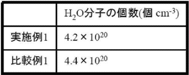
表2より、比較例1より実験例1の方が膜中H2O分子が多いことが分かる。
即ち、酸化物半導体薄膜形成後の熱処理の方法によって酸化物半導体薄膜中のH2O分子の個数に差が生じる事が分かった。特に、実験例1と比較例1においては、熱処理雰囲気が水分を含むか否かの違いがあることから、アニール雰囲気に含まれる水分量によって酸化物半導体膜中に含まれるH2O分子に差が生じることを意味している。
-活性層膜中水分量の違いによるTFT特性の変化-
膜中の水分が異なる酸化物半導体薄膜を、TFTの活性層に用いたときにTFT特性にどのような影響を与えるか以下の実験を行い検証した。
膜中の水分が異なる酸化物半導体薄膜を、TFTの活性層に用いたときにTFT特性にどのような影響を与えるか以下の実験を行い検証した。
<実験例2>
実験例2として、ボトムゲート構造でトップコンタクト型のTFTを評価用サンプルとして作製した。
実験例2として、ボトムゲート構造でトップコンタクト型のTFTを評価用サンプルとして作製した。
図9(A)は実験例2のTFTの平面図であり、図9(B)は図9(A)に示すTFTのA-A線矢視断面図である。
実験例2のTFT500は、具体的に以下のように作製した。
基板502として、100nmのSiO2の酸化膜504が表面上に形成された高濃度ドープされたp型シリコン基板(三菱マテリアル社製)を用いた。活性層506として基板502上にIn:Ga:Zn=1:1:1組成のIGZO層を45nm成膜した。IGZO層はIn2O3ターゲット、Ga2O3ターゲット、ZnOターゲットを用いた共スパッタ(co-sputter)法にて行った。IGZO層の詳細なスパッタ条件は実験例1の酸化物半導体薄膜の条件と同じである。
基板502として、100nmのSiO2の酸化膜504が表面上に形成された高濃度ドープされたp型シリコン基板(三菱マテリアル社製)を用いた。活性層506として基板502上にIn:Ga:Zn=1:1:1組成のIGZO層を45nm成膜した。IGZO層はIn2O3ターゲット、Ga2O3ターゲット、ZnOターゲットを用いた共スパッタ(co-sputter)法にて行った。IGZO層の詳細なスパッタ条件は実験例1の酸化物半導体薄膜の条件と同じである。
活性層506形成後に、酸素分圧制御炉中において全圧が大気圧で、アルゴンと酸素の分圧比Ar/O2=80/20(全体に対する酸素分圧Po2anneal=20%)の雰囲気下において200℃でアニール処理を行った。アルゴンと酸素はガスボンベから供給されており、乾燥雰囲気下で熱処理を行っている。熱処理後、メタルマスクを介してTi/Au電極をそれぞれ10nm/40nmの厚みになるよう蒸着し、ソース・ドレイン電極510,512を形成した。以上により、チャネル長180μm、チャネル幅1mmの実験例2に係るボトムゲート型薄膜トランジスタ500を得た。即ち、実験例2は実験例1と同じく膜中にH2O分子を4.2×1020cm-3個含む酸化物半導体薄膜を活性層に備えた薄膜トランジスタである。
<比較例2>
比較例2のTFTとして、熱処理を大気中(湿度66%)で行い、それ以外は全て同じ方法で作製したものを用意した。即ち、比較例2は比較例1と同じく膜中にH2O分子を4.4×1020cm-3個含む酸化物半導体薄膜を活性層に備えたTFTである。
比較例2のTFTとして、熱処理を大気中(湿度66%)で行い、それ以外は全て同じ方法で作製したものを用意した。即ち、比較例2は比較例1と同じく膜中にH2O分子を4.4×1020cm-3個含む酸化物半導体薄膜を活性層に備えたTFTである。
<評価>
上記実験例2及び比較例2のTFTについて、半導体パラメータ・アナライザー4156C(アジレントテクノロジー社製)を用い、トランジスタ特性(Vg-Id特性)および電界効果移動度μの測定を行った。測定結果を図10に示した。Vg-Id特性の測定は、ドレイン電圧(Vd)を10Vに固定し、ゲート電圧(Vg)を-15V~+15Vの範囲内で変化させ、各ゲート電圧(Vg)におけるドレイン電流(Id)を測定することにて行った。また、上記測定方法は以下の実験例においても同様に適用した。
上記実験例2及び比較例2のTFTについて、半導体パラメータ・アナライザー4156C(アジレントテクノロジー社製)を用い、トランジスタ特性(Vg-Id特性)および電界効果移動度μの測定を行った。測定結果を図10に示した。Vg-Id特性の測定は、ドレイン電圧(Vd)を10Vに固定し、ゲート電圧(Vg)を-15V~+15Vの範囲内で変化させ、各ゲート電圧(Vg)におけるドレイン電流(Id)を測定することにて行った。また、上記測定方法は以下の実験例においても同様に適用した。
測定結果から算出した、実験例2及び比較例2のTFTの閾値電圧(Vth)及び電界効果移動度を表3に示す。閾値電圧(Vth)は飽和領域の電流値Idsatを計測し、Idsat=WCμsat(Vgs―Vth)2/2Lの式を用い算出した。ここで、Wは活性層のチャネル幅、Lは活性層のチャネル長さ、Cはゲート絶縁膜の単位面積あたりの静電容量、Vgsはゲート-ソース電極間にかかる電圧、μsatは飽和移動度である。また、移動度値は、Vd=1Vに固定し、ゲート電圧(Vg)を-15V~+15Vの範囲内で掃引して測定したIdから、線形移動度を算出し記載している。

図10及び表3から実験例2及び比較例2のTFTは共に、On/Off比が105を上回る良好なスイッチング特性を示している他、両者とも10cm2/Vsを超える高い移動度を示している。一方で、比較例2では閾値電圧が-10.5Vとノーマリーオン特性を示すことがわかった。
一般的に低消費電力の観点から、ノーマリーオン駆動よりも、ノーマリーオフ駆動のTFTの方がより好ましいとされており、実験例1の方がより好ましい半導体特性を示すTFTであることが分かった。
このような両者の特性の差異は熱処理の方法によるものであり、上記結果は熱処理雰囲気に含まれる水分が活性層に余剰キャリアを誘起する事を示唆するものである。
従って、乾燥雰囲気下において熱処理することが所望の半導体特性を得るために極めて有効であることが分かった。
また、実験例2及び比較例2のTFTの活性層膜中H2O分子個数の比較から、活性層膜中のH2O分子が4.4×1020cm-3個以上であるとノーマリーオン特性になることが分かった。従って、高移動度・ノーマリーオフ駆動を同時に実現するためには、乾燥雰囲気下において熱処理を行い、膜中H2O分子が4.2×1020cm-3個以下の酸化物半導体薄膜を活性層に用いることが有効であることが分かった。
-アニール時の酸素分圧と活性層成膜時の導入酸素分圧-
次に、乾燥雰囲気下において行う熱処理において、熱処理時の酸素分圧及び、活性層成膜時の導入酸素分圧を系統的に変化させ、TFT特性の評価を行った。具体的には以下のサンプルを作製し、TFT特性の評価を行った。
次に、乾燥雰囲気下において行う熱処理において、熱処理時の酸素分圧及び、活性層成膜時の導入酸素分圧を系統的に変化させ、TFT特性の評価を行った。具体的には以下のサンプルを作製し、TFT特性の評価を行った。
<実験例3~8>
実験例1とはアニール条件のみが異なっており、熱処理時のAr/O2分圧を100/0、95/5、90/10、85/15、80/20、0/100(つまり酸素分圧Po2annealが0、5、10、15、20、100%。左から順に実験例3~8)と系統的に変化させた6試料を作製した。
実験例1とはアニール条件のみが異なっており、熱処理時のAr/O2分圧を100/0、95/5、90/10、85/15、80/20、0/100(つまり酸素分圧Po2annealが0、5、10、15、20、100%。左から順に実験例3~8)と系統的に変化させた6試料を作製した。
<比較例3>
また、実験例3と同一の製造工程を行い、ウェットアニール処理を行って作製したTFTを比較例3とした。
また、実験例3と同一の製造工程を行い、ウェットアニール処理を行って作製したTFTを比較例3とした。
<実験例9~14>
実験例9~14では、実験例1とは活性層成膜時の酸素分圧と、熱処理時の酸素分圧を変化させている。活性層成膜時の酸素分圧を2.0%にし、その他組成等の条件は変化させていない。スパッタ条件は実験例1と同じである。
実験例9~14では、実験例1とは活性層成膜時の酸素分圧と、熱処理時の酸素分圧を変化させている。活性層成膜時の酸素分圧を2.0%にし、その他組成等の条件は変化させていない。スパッタ条件は実験例1と同じである。
その上で、熱処理時の酸素分圧を0、5、10、15、20、100%(左から順に実験例9~14)と系統的に変化させた6試料を作製した。
<比較例4>
また、実験例9と同一の製造工程を行い、ウェットアニール処理を行って作製したTFTを比較例4とした。
また、実験例9と同一の製造工程を行い、ウェットアニール処理を行って作製したTFTを比較例4とした。
<実験例15~20>
実験例15~20では、同様に、活性層成膜時の導入酸素分圧と、熱処理時の酸素分圧を変化させている。活性層成膜時の酸素分圧を6.3%にし、その他組成等の条件は変化させていない。スパッタ条件は実験例1と同じである。
実験例15~20では、同様に、活性層成膜時の導入酸素分圧と、熱処理時の酸素分圧を変化させている。活性層成膜時の酸素分圧を6.3%にし、その他組成等の条件は変化させていない。スパッタ条件は実験例1と同じである。
その上で、熱処理時の酸素分圧を0、5、10、15、20、100%(左から順に実験例15~20)と系統的に変化させた6試料を作製した。
<比較例5>
また、実験例15と同一の製造工程を行い、ウェットアニール処理を行って作製したTFTを比較例5とした。
また、実験例15と同一の製造工程を行い、ウェットアニール処理を行って作製したTFTを比較例5とした。
<評価>
これら実験例3~20及び比較例3~5においてVg-Id特性の測定を行ったものを図11A~11Cに示す。また、熱処理時の酸素分圧及び、活性層成膜時の酸素分圧の条件、サンプル名、閾値電圧、及び電界効果移動度についてまとめたものを表4に示す。
これら実験例3~20及び比較例3~5においてVg-Id特性の測定を行ったものを図11A~11Cに示す。また、熱処理時の酸素分圧及び、活性層成膜時の酸素分圧の条件、サンプル名、閾値電圧、及び電界効果移動度についてまとめたものを表4に示す。
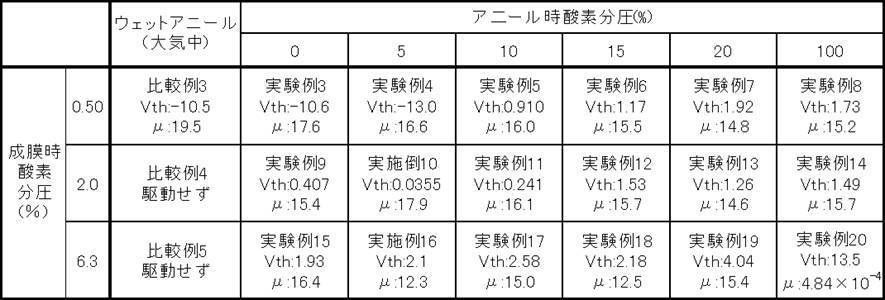
図11A~C、表4より、幅広い酸素分圧範囲でノーマリーオフ駆動の素子が得られている事から、プロセスマージンが広い特性制御手法であることが分かった。特に、活性層の成膜条件によっては熱処理雰囲気に酸素を含まなくてもノーマリーオフ駆動の素子が得られた。これは乾燥雰囲気下での熱処理が、低温プロセスにおいて本質的に有効であることを意味している。
具体的に、表4に示す結果から、ノーマリーオフ駆動で且つ電界効果移動度が10cm2/Vs以上のTFTは、図12に示す点線で囲まれる範囲であることが分かった。なお、図12は活性層成膜時の酸素分圧と熱処理時の酸素分圧との関係を示す図であり、本発明の実験例のうち図中○は、実施例となり、×は比較例となる。
そして、この範囲は、成膜工程での前記成膜室中の雰囲気の全圧に対する酸素分圧をPo2depo(%)とし、熱処理工程中の雰囲気の全圧に対する酸素分圧をPo2anneal(%)としたときに、熱処理工程時の酸素分圧Po2anneal(%)が、-20/3Po2depo+40/3≦Po2anneal≦-800/43Po2depo+5900/43の範囲で表されることが分かった。
そして、この範囲は、成膜工程での前記成膜室中の雰囲気の全圧に対する酸素分圧をPo2depo(%)とし、熱処理工程中の雰囲気の全圧に対する酸素分圧をPo2anneal(%)としたときに、熱処理工程時の酸素分圧Po2anneal(%)が、-20/3Po2depo+40/3≦Po2anneal≦-800/43Po2depo+5900/43の範囲で表されることが分かった。
また、特に成膜時の酸素分圧Po2depo(%)が0.50%以上であると、ノーマリーオフ駆動が得られる酸素分圧条件が十分広く、プロセスマージンの観点から好ましい。
また、活性層成膜時の酸素分圧Po2depo(%)が6.3%の時には全てノーマリーオフ駆動が得られているものの、アニール時の酸素分圧が100%の時には移動度が低減することが分かった。従って活性層成膜時の酸素分圧Po2depo(%)は6.3%以下であることがより好ましい。
-活性層成膜時の酸素分圧の下限値-
次に、活性層成膜時の酸素分圧Po2depo(%)の下限値について、IGZO膜のホール移動度を測定して決定した。
次に、活性層成膜時の酸素分圧Po2depo(%)の下限値について、IGZO膜のホール移動度を測定して決定した。
<実験例21>
実験例21では、上記のようにTFTは作製せず、基板上に、成膜室中の雰囲気の全圧に対する酸素分圧Po2depo(%)を0.17%未満にして、組成比がIn:Ga:Zn=1:1:1のIGZO膜を成膜した。そして、この成膜した膜のホール移動度を測定した。同様に、上記のようにTFTは作製せず、基板上に、成膜室中の雰囲気の全圧に対する酸素分圧Po2depo(%)を0.50%にして、組成比がIn:Ga:Zn=1:1:1のIGZO膜を成膜した。そして、この成膜した膜のホール移動度を測定した。
2つのIGZO膜について、ホール移動度を測定した結果を表5に示す。
実験例21では、上記のようにTFTは作製せず、基板上に、成膜室中の雰囲気の全圧に対する酸素分圧Po2depo(%)を0.17%未満にして、組成比がIn:Ga:Zn=1:1:1のIGZO膜を成膜した。そして、この成膜した膜のホール移動度を測定した。同様に、上記のようにTFTは作製せず、基板上に、成膜室中の雰囲気の全圧に対する酸素分圧Po2depo(%)を0.50%にして、組成比がIn:Ga:Zn=1:1:1のIGZO膜を成膜した。そして、この成膜した膜のホール移動度を測定した。
2つのIGZO膜について、ホール移動度を測定した結果を表5に示す。
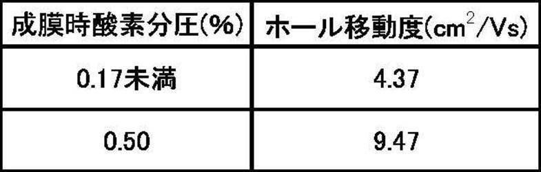
表5より、成膜時酸素分圧が0.17%未満で成膜した場合、酸素分圧が0.50%で成膜した場合と比較して、同じ組成でもホール移動度が半分以下になることが分かった。そのため、成膜時酸素分圧は0.17%以上であることが好ましく、更にキャリア濃度制御と移動度の観点から、成膜時酸素分圧は0.50%以上であることがより好ましいことが確認できた。
-熱処理時の温度依存性-
熱処理が異なる温度範囲においても有効であることを実証するため、熱処理時の温度を系統的に変化させたサンプルを作製し、Vg-Id特性の評価を行った。
熱処理が異なる温度範囲においても有効であることを実証するため、熱処理時の温度を系統的に変化させたサンプルを作製し、Vg-Id特性の評価を行った。
<実験例22~24>
熱処理条件以外は実験例2と同様であり、熱処理の温度は150℃とした。熱処理時の酸素分圧は系統的に10%、20%、100%とし、それぞれ実験例22、23、24とした。
熱処理条件以外は実験例2と同様であり、熱処理の温度は150℃とした。熱処理時の酸素分圧は系統的に10%、20%、100%とし、それぞれ実験例22、23、24とした。
<実験例25~27>
熱処理条件以外は実験例2と同様であり、熱処理の温度は200℃とした。熱処理時の酸素分圧は系統的に10%、20%、100%とし、それぞれ実験例25、26、27とした。
熱処理条件以外は実験例2と同様であり、熱処理の温度は200℃とした。熱処理時の酸素分圧は系統的に10%、20%、100%とし、それぞれ実験例25、26、27とした。
<実験例28~30>
熱処理条件以外は実験例2と同様であり、熱処理の温度は250℃とした。熱処理時の酸素分圧は系統的に10%、20%、100%とし、それぞれ実験例28、29、30とした。
熱処理条件以外は実験例2と同様であり、熱処理の温度は250℃とした。熱処理時の酸素分圧は系統的に10%、20%、100%とし、それぞれ実験例28、29、30とした。
<実験例31>
熱処理条件以外は実験例2と同様であり、熱処理の温度は300℃とした。熱処理時の酸素分圧は系統的に20%とし、実験例31とした。
熱処理条件以外は実験例2と同様であり、熱処理の温度は300℃とした。熱処理時の酸素分圧は系統的に20%とし、実験例31とした。
これら実験例22~30(31は省略)においてVg-Id特性の測定を行った結果を図13A~Cに示す。また、熱処理時の温度、熱処理時の酸素分圧の条件、サンプル名、閾値電圧、移動度についてまとめたものを表6に示す。

図13A~C、及び表6より、特に酸素分圧が100%の条件において150℃以上300℃未満の温度範囲では熱処理温度に依存せず、ノーマリーオフ駆動、移動度10cm2/Vs以上の良好なTFT特性を示すトランジスタが得られることがわかる。従って、乾燥雰囲気における熱処理によって300℃未満の幅広い温度範囲において所望の半導体特性を得ることが可能である。なお、150℃では、ノーマリーオフ駆動でないものものあるが、組成や成膜条件を適宜調整すれば、ノーマリーオフ駆動になるものと考える。
-活性層の組成依存性-
そこで、活性層の組成が異なる場合においても有効であることを実証するため、活性層のIGZO組成を系統的に変化させたサンプルを作製し、Vg-Id特性と移動度の評価を行った。
そこで、活性層の組成が異なる場合においても有効であることを実証するため、活性層のIGZO組成を系統的に変化させたサンプルを作製し、Vg-Id特性と移動度の評価を行った。
<実験例32~36>
活性層の組成と熱処理条件以外は実験例2と同様であり、熱処理の温度は200℃とした。熱処理時の酸素分圧は20%とし、IGZO組成をGa/(In+Ga)比で0.25、0.375、0.625、0.75、0.9と変化させ、それぞれ実験例32~36とした。
活性層の組成と熱処理条件以外は実験例2と同様であり、熱処理の温度は200℃とした。熱処理時の酸素分圧は20%とし、IGZO組成をGa/(In+Ga)比で0.25、0.375、0.625、0.75、0.9と変化させ、それぞれ実験例32~36とした。
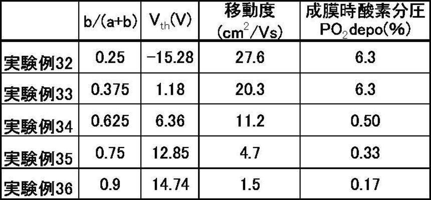
表7に示す結果から、他の条件は考慮せず組成だけ考えると、Ga/(In+Ga)比が、0.375以上0.9以下の条件でノーマリーオフ駆動が可能であることが分かった。また、Ga/(In+Ga)比が、0.375以上0.625以下の条件でノーマリーオフ駆動、電界効果移動度10cm2/Vs以上が得られることが分かった。
Claims (13)
- In,Ga及びZnのうち少なくとも2種類の元素とOで構成される酸化物半導体を主成分として含有する活性層を、少なくとも酸素を導入した成膜室内で成膜する成膜工程と、乾燥雰囲気下において前記活性層を300℃未満で熱処理する熱処理工程と、を有する薄膜トランジスタの製造方法であって、
前記成膜工程での前記成膜室中の雰囲気の全圧に対する酸素分圧をPo2depo(%)とし、前記熱処理工程中の雰囲気の全圧に対する酸素分圧をPo2anneal(%)としたときに、前記熱処理工程時の酸素分圧Po2anneal(%)が、-20/3Po2depo+40/3≦Po2anneal≦-800/43Po2depo+5900/43の関係を満たすように前記成膜工程と前記熱処理工程とを行う、
薄膜トランジスタの製造方法。 - 前記成膜工程では、前記酸素分圧Po2depoを0.17%以上とする、
請求項1の薄膜トランジスタの製造方法。 - 前記成膜工程では、前記酸素分圧Po2depoを0.50%以上とする、
請求項2の薄膜トランジスタの製造方法。 - 前記成膜工程では、前記酸素分圧Po2depoを6.3%以下とする、
請求項1の薄膜トランジスタの製造方法。 - 前記熱処理工程では、熱処理温度を150℃超とする、
請求項1の薄膜トランジスタの製造方法。 - 前記熱処理工程では、熱処理温度を250℃以下とする、
請求項1の薄膜トランジスタの製造方法。 - 前記酸化物半導体は、In,Ga,Zn及びOで構成され、前記Inのモル比と前記Gaのモル比との合計に対する前記Gaのモル比が0.375≦Ga/(In+Ga)≦0.625の関係を満たす、
請求項1の薄膜トランジスタの製造方法。 - 前記成膜工程では、前記活性層を、スパッタリング法で成膜する、
請求項1の薄膜トランジスタの製造方法。 - 請求項1~請求項8の何れか1項の薄膜トランジスタの製造方法を用いて作製した薄膜トランジスタであって、
前記活性層は、昇温脱離ガス分析により観測されるH2O分子の個数が4.2×1020cm-3以下である、
薄膜トランジスタ。 - 前記活性層は、可撓性を有する基板上に形成されている、
請求項9の薄膜トランジスタ。 - 請求項9の薄膜トランジスタを備えた表示装置。
- 請求項9の薄膜トランジスタを備えたセンサ。
- 請求項12のセンサを備えたX線デジタル撮影装置。
Priority Applications (2)
| Application Number | Priority Date | Filing Date | Title |
|---|---|---|---|
| KR1020137022092A KR101634101B1 (ko) | 2011-03-11 | 2012-02-22 | 박막 트랜지스터의 제조 방법, 박막 트랜지스터, 표시 장치, 센서 및 x 선 디지털 촬영 장치 |
| US13/963,061 US9236454B2 (en) | 2011-03-11 | 2013-08-09 | Method of manufacturing thin-film transistor, thin-film transistor, display apparatus, sensor, and digital X-ray image-capturing apparatus |
Applications Claiming Priority (2)
| Application Number | Priority Date | Filing Date | Title |
|---|---|---|---|
| JP2011-054718 | 2011-03-11 | ||
| JP2011054718A JP5657433B2 (ja) | 2011-03-11 | 2011-03-11 | 薄膜トランジスタの製造方法、薄膜トランジスタ、表示装置、センサ及びx線デジタル撮影装置 |
Related Child Applications (1)
| Application Number | Title | Priority Date | Filing Date |
|---|---|---|---|
| US13/963,061 Continuation US9236454B2 (en) | 2011-03-11 | 2013-08-09 | Method of manufacturing thin-film transistor, thin-film transistor, display apparatus, sensor, and digital X-ray image-capturing apparatus |
Publications (1)
| Publication Number | Publication Date |
|---|---|
| WO2012124444A1 true WO2012124444A1 (ja) | 2012-09-20 |
Family
ID=46830520
Family Applications (1)
| Application Number | Title | Priority Date | Filing Date |
|---|---|---|---|
| PCT/JP2012/054318 Ceased WO2012124444A1 (ja) | 2011-03-11 | 2012-02-22 | 薄膜トランジスタの製造方法、薄膜トランジスタ、表示装置、センサ及びx線デジタル撮影装置 |
Country Status (5)
| Country | Link |
|---|---|
| US (1) | US9236454B2 (ja) |
| JP (1) | JP5657433B2 (ja) |
| KR (1) | KR101634101B1 (ja) |
| TW (1) | TWI511202B (ja) |
| WO (1) | WO2012124444A1 (ja) |
Cited By (2)
| Publication number | Priority date | Publication date | Assignee | Title |
|---|---|---|---|---|
| CN103728797A (zh) * | 2013-12-25 | 2014-04-16 | 合肥京东方光电科技有限公司 | 显示面板及其制作方法和显示装置 |
| US11309181B2 (en) | 2016-06-06 | 2022-04-19 | Semiconductor Energy Laboratory Co., Ltd. | Sputtering apparatus, sputtering target, and method for forming semiconductor film with the sputtering apparatus |
Families Citing this family (15)
| Publication number | Priority date | Publication date | Assignee | Title |
|---|---|---|---|---|
| JP5920967B2 (ja) * | 2011-09-20 | 2016-05-24 | 株式会社アルバック | Igzo膜の形成方法及び薄膜トランジスタの製造方法 |
| JP5960626B2 (ja) * | 2013-03-08 | 2016-08-02 | 富士フイルム株式会社 | 薄膜トランジスタを備えた半導体装置の製造方法 |
| JP6207869B2 (ja) * | 2013-04-12 | 2017-10-04 | 三井造船株式会社 | 半導体素子の製造方法 |
| TWI560882B (en) * | 2014-01-17 | 2016-12-01 | E Ink Holdings Inc | Semiconductor structure |
| US20150311345A1 (en) * | 2014-04-28 | 2015-10-29 | Boe Technology Group Co., Ltd. | Thin film transistor and method of fabricating the same, display substrate and display device |
| CN104143575A (zh) * | 2014-07-25 | 2014-11-12 | 京东方科技集团股份有限公司 | 一种薄膜晶体管、阵列基板和显示装置 |
| US20160231097A1 (en) * | 2014-08-22 | 2016-08-11 | The Regents Of The University Of Michigan | Patterned Nano-Engineered Thin Films On Flexible Substrates For Sensing Applications |
| JP6358596B2 (ja) * | 2014-11-27 | 2018-07-18 | 株式会社Joled | 薄膜トランジスタ基板の製造方法 |
| KR102569928B1 (ko) * | 2016-05-18 | 2023-08-24 | 삼성디스플레이 주식회사 | 플렉서블 디스플레이 |
| TWI613804B (zh) | 2017-09-04 | 2018-02-01 | 友達光電股份有限公司 | 光感測裝置 |
| CN109755342B (zh) * | 2017-11-06 | 2020-10-27 | 中国科学院物理研究所 | 一种直接型x射线探测器及其制备方法 |
| US12114515B2 (en) | 2018-12-21 | 2024-10-08 | National Research Council Of Canada | Thin film transistors comprising carbon nanotube networks encapsulated by a polymeric layer and methods for the manufacture thereof |
| KR102439997B1 (ko) * | 2020-10-28 | 2022-09-05 | 충북대학교 산학협력단 | 산화물 반도체에서 상부 전극 제조 장치 및 방법 |
| KR102439996B1 (ko) * | 2020-10-28 | 2022-09-05 | 충북대학교 산학협력단 | 산화물 반도체에서 산화물층 제조 장치 및 방법 |
| CN114134475A (zh) * | 2021-12-01 | 2022-03-04 | 合肥工业大学 | 一种高迁移率、高透光igzo薄膜的制备方法及其应用 |
Citations (3)
| Publication number | Priority date | Publication date | Assignee | Title |
|---|---|---|---|---|
| JP2006165530A (ja) * | 2004-11-10 | 2006-06-22 | Canon Inc | センサ及び非平面撮像装置 |
| JP2011014761A (ja) * | 2009-07-03 | 2011-01-20 | Fujifilm Corp | ボトムゲート構造の薄膜トランジスタの製造方法 |
| JP2011035389A (ja) * | 2009-07-10 | 2011-02-17 | Semiconductor Energy Lab Co Ltd | 半導体装置の作製方法 |
Family Cites Families (3)
| Publication number | Priority date | Publication date | Assignee | Title |
|---|---|---|---|---|
| US7453065B2 (en) | 2004-11-10 | 2008-11-18 | Canon Kabushiki Kaisha | Sensor and image pickup device |
| JP5127183B2 (ja) | 2006-08-23 | 2013-01-23 | キヤノン株式会社 | アモルファス酸化物半導体膜を用いた薄膜トランジスタの製造方法 |
| JP2010238770A (ja) | 2009-03-30 | 2010-10-21 | Nippon Mining & Metals Co Ltd | 酸化物薄膜及びその製造方法 |
-
2011
- 2011-03-11 JP JP2011054718A patent/JP5657433B2/ja active Active
-
2012
- 2012-02-20 TW TW101105501A patent/TWI511202B/zh active
- 2012-02-22 KR KR1020137022092A patent/KR101634101B1/ko active Active
- 2012-02-22 WO PCT/JP2012/054318 patent/WO2012124444A1/ja not_active Ceased
-
2013
- 2013-08-09 US US13/963,061 patent/US9236454B2/en active Active
Patent Citations (3)
| Publication number | Priority date | Publication date | Assignee | Title |
|---|---|---|---|---|
| JP2006165530A (ja) * | 2004-11-10 | 2006-06-22 | Canon Inc | センサ及び非平面撮像装置 |
| JP2011014761A (ja) * | 2009-07-03 | 2011-01-20 | Fujifilm Corp | ボトムゲート構造の薄膜トランジスタの製造方法 |
| JP2011035389A (ja) * | 2009-07-10 | 2011-02-17 | Semiconductor Energy Lab Co Ltd | 半導体装置の作製方法 |
Cited By (2)
| Publication number | Priority date | Publication date | Assignee | Title |
|---|---|---|---|---|
| CN103728797A (zh) * | 2013-12-25 | 2014-04-16 | 合肥京东方光电科技有限公司 | 显示面板及其制作方法和显示装置 |
| US11309181B2 (en) | 2016-06-06 | 2022-04-19 | Semiconductor Energy Laboratory Co., Ltd. | Sputtering apparatus, sputtering target, and method for forming semiconductor film with the sputtering apparatus |
Also Published As
| Publication number | Publication date |
|---|---|
| JP5657433B2 (ja) | 2015-01-21 |
| US9236454B2 (en) | 2016-01-12 |
| KR20140006901A (ko) | 2014-01-16 |
| KR101634101B1 (ko) | 2016-06-28 |
| TW201239989A (en) | 2012-10-01 |
| TWI511202B (zh) | 2015-12-01 |
| JP2012191072A (ja) | 2012-10-04 |
| US20130320338A1 (en) | 2013-12-05 |
Similar Documents
| Publication | Publication Date | Title |
|---|---|---|
| JP5657433B2 (ja) | 薄膜トランジスタの製造方法、薄膜トランジスタ、表示装置、センサ及びx線デジタル撮影装置 | |
| JP5606787B2 (ja) | 薄膜トランジスタの製造方法、並びに、薄膜トランジスタ、イメージセンサー、x線センサー及びx線デジタル撮影装置 | |
| JP4982620B1 (ja) | 電界効果型トランジスタの製造方法、並びに、電界効果型トランジスタ、表示装置、イメージセンサ及びx線センサ | |
| JP5052693B1 (ja) | 薄膜トランジスタ及びその製造方法、表示装置、イメージセンサー、x線センサー並びにx線デジタル撮影装置 | |
| JP5497417B2 (ja) | 薄膜トランジスタおよびその製造方法、並びにその薄膜トランジスタを備えた装置 | |
| JP5679933B2 (ja) | 薄膜トランジスタ及びその製造方法、表示装置、イメージセンサー、x線センサー並びにx線デジタル撮影装置 | |
| JP5615744B2 (ja) | 電界効果型トランジスタ、表示装置、センサ及び電界効果型トランジスタの製造方法 | |
| TWI580048B (zh) | 場效電晶體的製造方法 | |
| WO2013161570A1 (ja) | 電界効果型トランジスタ及びその製造方法、表示装置、イメージセンサ並びにx線センサ | |
| KR101687468B1 (ko) | 박막 트랜지스터 및 그 제조 방법, 표시 장치, 이미지 센서, x 선 센서 그리고 x 선 디지털 촬영 장치 | |
| JP5869110B2 (ja) | 薄膜トランジスタ、表示装置、イメージセンサ及びx線センサ | |
| KR101717336B1 (ko) | 박막 트랜지스터의 제조 방법 | |
| WO2012124408A1 (ja) | 酸化物半導体薄膜の製造方法 |
Legal Events
| Date | Code | Title | Description |
|---|---|---|---|
| 121 | Ep: the epo has been informed by wipo that ep was designated in this application |
Ref document number: 12757166 Country of ref document: EP Kind code of ref document: A1 |
|
| ENP | Entry into the national phase |
Ref document number: 20137022092 Country of ref document: KR Kind code of ref document: A |
|
| NENP | Non-entry into the national phase |
Ref country code: DE |
|
| 122 | Ep: pct application non-entry in european phase |
Ref document number: 12757166 Country of ref document: EP Kind code of ref document: A1 |