WO2012124063A1 - 半導体記憶装置及び半導体記憶装置の制御方法 - Google Patents
半導体記憶装置及び半導体記憶装置の制御方法 Download PDFInfo
- Publication number
- WO2012124063A1 WO2012124063A1 PCT/JP2011/056109 JP2011056109W WO2012124063A1 WO 2012124063 A1 WO2012124063 A1 WO 2012124063A1 JP 2011056109 W JP2011056109 W JP 2011056109W WO 2012124063 A1 WO2012124063 A1 WO 2012124063A1
- Authority
- WO
- WIPO (PCT)
- Prior art keywords
- data
- column
- selection data
- sub
- sel
- Prior art date
- Legal status (The legal status is an assumption and is not a legal conclusion. Google has not performed a legal analysis and makes no representation as to the accuracy of the status listed.)
- Ceased
Links
Images














Classifications
-
- G—PHYSICS
- G11—INFORMATION STORAGE
- G11C—STATIC STORES
- G11C11/00—Digital stores characterised by the use of particular electric or magnetic storage elements; Storage elements therefor
- G11C11/21—Digital stores characterised by the use of particular electric or magnetic storage elements; Storage elements therefor using electric elements
- G11C11/34—Digital stores characterised by the use of particular electric or magnetic storage elements; Storage elements therefor using electric elements using semiconductor devices
- G11C11/40—Digital stores characterised by the use of particular electric or magnetic storage elements; Storage elements therefor using electric elements using semiconductor devices using transistors
- G11C11/41—Digital stores characterised by the use of particular electric or magnetic storage elements; Storage elements therefor using electric elements using semiconductor devices using transistors forming static cells with positive feedback, i.e. cells not needing refreshing or charge regeneration, e.g. bistable multivibrator or Schmitt trigger
- G11C11/413—Auxiliary circuits, e.g. for addressing, decoding, driving, writing, sensing, timing or power reduction
- G11C11/417—Auxiliary circuits, e.g. for addressing, decoding, driving, writing, sensing, timing or power reduction for memory cells of the field-effect type
- G11C11/419—Read-write [R-W] circuits
-
- G—PHYSICS
- G11—INFORMATION STORAGE
- G11C—STATIC STORES
- G11C11/00—Digital stores characterised by the use of particular electric or magnetic storage elements; Storage elements therefor
- G11C11/21—Digital stores characterised by the use of particular electric or magnetic storage elements; Storage elements therefor using electric elements
- G11C11/34—Digital stores characterised by the use of particular electric or magnetic storage elements; Storage elements therefor using electric elements using semiconductor devices
- G11C11/40—Digital stores characterised by the use of particular electric or magnetic storage elements; Storage elements therefor using electric elements using semiconductor devices using transistors
- G11C11/41—Digital stores characterised by the use of particular electric or magnetic storage elements; Storage elements therefor using electric elements using semiconductor devices using transistors forming static cells with positive feedback, i.e. cells not needing refreshing or charge regeneration, e.g. bistable multivibrator or Schmitt trigger
- G11C11/413—Auxiliary circuits, e.g. for addressing, decoding, driving, writing, sensing, timing or power reduction
- G11C11/417—Auxiliary circuits, e.g. for addressing, decoding, driving, writing, sensing, timing or power reduction for memory cells of the field-effect type
- G11C11/418—Address circuits
-
- G—PHYSICS
- G11—INFORMATION STORAGE
- G11C—STATIC STORES
- G11C8/00—Arrangements for selecting an address in a digital store
- G11C8/08—Word line control circuits, e.g. drivers, boosters, pull-up circuits, pull-down circuits, precharging circuits, for word lines
-
- G—PHYSICS
- G11—INFORMATION STORAGE
- G11C—STATIC STORES
- G11C8/00—Arrangements for selecting an address in a digital store
- G11C8/10—Decoders
Definitions
- the present invention relates to a semiconductor memory device and a method for controlling the semiconductor memory device.
- the matrix is controlled to prevent the parity from becoming invalid.
- the semiconductor memory device having a plurality of memory cells arranged in the same manner, there is a semiconductor memory device in which bit lines connected to the same bit line selection circuit are arranged so as not to be adjacent to each other.
- the soft error as described above is caused by the incidence of charged ⁇ -rays or the like among cosmic rays or neutrons or the like having no charge to the semiconductor memory device.
- bit lines connected to the same bit line selection circuit are arranged so as not to be adjacent to each other, the wiring length of the bit lines becomes long, and the layout and operation speed are restricted.
- bit lines connected to the same bit line selection circuit are arranged so as not to be adjacent to each other is not suitable for a semiconductor memory device such as an SRAM (StaticStatRandom Access Memory) operating at a high frequency.
- SRAM StaticStatRandom Access Memory
- the increase in the number of columns has a problem that the operation speed is lowered due to a change in the aspect ratio (horizontal length) of the semiconductor memory device and an increase in the length of the word line.
- an object of the present invention is to provide a semiconductor memory device and a method for controlling the semiconductor memory device in which occurrence of data destruction over a plurality of bits is suppressed while suppressing a change in aspect ratio and a decrease in operation speed.
- a semiconductor memory device when a plurality of memory blocks each having a plurality of memory cells holding data and a plurality of memory cells having the same address are specified, adjacent memory bits in different memory blocks A decoder for specifying a memory cell; and a read / write controller that executes reading of data held in the memory cell specified by the decoder and writing of data to the memory cell specified by the decoder.
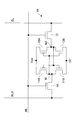
- FIG. 1 is a diagram schematically showing a structure of a single port type bit cell 10 used in an SRAM.
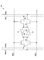
- FIG. It is a figure which shows the structure of the bit cell 10 of FIG. 1 in detail. It is a figure which shows an 8-transistor type multi-port bit cell.
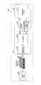
- 1 is a diagram illustrating an information processing apparatus including a semiconductor memory device according to a first embodiment. It is a figure which expands and shows the semiconductor memory device of FIG. 2 is a diagram showing a part of SRAM 200 according to the first embodiment.
- FIG. 3 is a diagram illustrating a data configuration of an input address of the SRAM 200 according to the first embodiment.
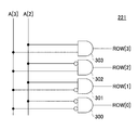
- FIG. 3 is a diagram illustrating a circuit of a row decoder 221 of the SRAM 200 according to the first embodiment.
- FIG. 3 is a diagram showing a circuit of a sub-block decoder 222 of the SRAM 200 according to the first embodiment.
- FIG. 3 is a diagram illustrating a circuit of an upper / lower selection decoder 223 of the SRAM 200 according to the first embodiment.
- FIG. 3 is a diagram illustrating a circuit of a pattern selection decoder 224 of the SRAM 200 according to the first embodiment.
- FIG. 3 is a diagram illustrating a circuit that decodes a column address included in a column decoder 225 of the SRAM 200 according to the first embodiment.
- FIG. 3 is a diagram illustrating a circuit that decodes a column address included in a column decoder 225 of the SRAM 200 according to the first embodiment.
- FIG. 3 is a diagram illustrating a circuit that decodes a column address included in a column decoder 225 of the SRAM 200 according to the first embodiment.
- FIG. 3 is a diagram illustrating a circuit that decodes a column address included in a column decoder 225 of the SRAM 200 according to the first embodiment.
- FIG. 3 is a diagram illustrating a circuit that decodes a column address included in a column decoder 225 of the SRAM 200 according to the first embodiment.
- FIG. 4 is a diagram showing a connection relationship between a column selection / read / write circuit 213 of the SRAM 200 of Embodiment 1 and a signal line for transmitting column selection data.
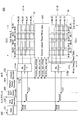
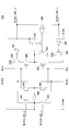
- FIG. 3 is a diagram showing a circuit of a column selection / read / write circuit 213 of the SRAM 100 according to the first embodiment.
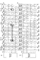
- FIG. FIG. 6 is a diagram showing how to select bits by the first pattern and the second pattern in the SRAM 200 of the first embodiment. 3 is a timing chart illustrating an operation example of the SRAM 200 according to the first embodiment. 6 is a diagram illustrating an operation example of the SRAM 200 according to the first embodiment.
- FIG. 6 is a diagram illustrating an operation example of the SRAM 200 according to the first embodiment.
- FIG. 6 is a diagram illustrating an operation example of the SRAM 200 according to the first embodiment.
- FIG. 6 is a diagram showing an SRAM 400 of a second embodiment. 6 is a diagram illustrating a switching circuit 215 of the SRAM 400 according to the second embodiment.
- FIG. FIG. 10 is a diagram showing a part of SRAM 400 according to the second embodiment.
- FIG. 10 is a diagram showing a data configuration of an input address of SRAM 400 according to the second embodiment.
- FIG. 10 is a diagram illustrating a circuit of a row decoder 421 of the SRAM 400 according to the second embodiment.
- FIG. 10 is a diagram illustrating a circuit of a subarray decoder 422 of the SRAM 400 according to the second embodiment.
- FIG. 10 is a diagram illustrating a circuit of a pattern selection decoder 423 of the SRAM 400 according to the second embodiment.
- FIG. 10 is a diagram illustrating a circuit of a column decoder 424 of the SRAM 400 according to the second embodiment.
- FIG. 10 is a diagram showing, by color, sub-blocks including bit cells having the same address in SRAM 400 of the second embodiment.
- FIG. 10 is a diagram showing, by color, sub-blocks including bit cells having the same address in SRAM 400 of the second embodiment.
- FIG. 10 is a diagram illustrating an SRAM 600 according to a third embodiment.
- FIG. 10 is a diagram showing a part of SRAM 600 of a third embodiment.
- FIG. 10 is a diagram showing a data configuration of an input address of SRAM 600 according to the third embodiment.
- FIG. 10 is a diagram illustrating a circuit of a row decoder 221 of the SRAM 600 according to the third embodiment.
- FIG. 10 is a diagram illustrating a circuit of a sub-block decoder 222 of the SRAM 600 according to the third embodiment.
- FIG. 10 is a diagram illustrating a circuit of a pattern selection decoder 623 of the SRAM 600 according to the third embodiment.
- FIG. 13 is a diagram showing a circuit of a region selection decoder 624 of the SRAM 600 according to the third embodiment.
- FIG. 20 is a diagram illustrating a circuit that decodes a column address included in a column decoder 625 of the SRAM 600 according to the third embodiment.
- FIG. 20 is a diagram illustrating a circuit that decodes a column address included in a column decoder 625 of the SRAM 600 according to the third embodiment.
- FIG. 20 is a diagram illustrating a circuit that decodes a column address included in a column decoder 625 of the SRAM 600 according to the third embodiment.
- FIG. 20 is a diagram illustrating a circuit that decodes a column address included in a column decoder 625 of the SRAM 600 according to the third embodiment.
- FIG. 1 is a diagram schematically showing the structure of a single-port bit cell 10 used in SRAM (Static Random Access Memory), and FIG. 2 is a diagram showing in detail the structure of the bit cell 10 of FIG.
- SRAM Static Random Access Memory
- the bit cell 10 includes a pair of inverters 11 and 12 which are negative circuits, and a pair of NMOS (N-type Metal Oxide Semiconductor) transistors 13 and 14.
- NMOS N-type Metal Oxide Semiconductor
- the inverters 11 and 12 are connected so as to form a loop.
- the gates of the NMOS transistors 13 and 14 are both connected to a word line WL (Word Line), the drain of the NMOS transistor 13 is connected to a positive bit line BL, and the drain of the NMOS transistor 14 is a negative bit line. It is connected to BLB (BL bar).
- the sources of the NMOS transistors 13 and 14 are connected to the connection portions N1 and N2 of the inverters 11 and 12 connected in a loop.
- the inverter 11 includes a CMOS (Complementary Metal Oxide Semiconductor) having a PMOS (P-type Metal Metal Oxide Semiconductor) transistor 11A and an NMOS transistor 11B.
- CMOS Complementary Metal Oxide Semiconductor
- PMOS P-type Metal Metal Oxide Semiconductor
- NMOS transistor 11B Type inverter
- the inverter 12 is a CMOS type inverter having a PMOS transistor 12A and an NMOS transistor 12B. That is, the bit cell shown in FIGS. 1 and 2 includes six MOS transistors.
- the input / output terminals of the MOS transistors 11A and 11B and the input / output terminals of the MOS transistors 12A and 12B are connected to cross each other, and the bit cell 10 is realized as a latch circuit including the inverters 11 and 12.
- connection portion N1 between the drains of the MOS transistors 11A and 11B corresponds to the connection portion N1 shown in FIG. 1 and functions as the storage node N1.
- connection portion N2 between the drains of the MOS transistors 12A and 12B corresponds to the connection portion N2 shown in FIG. 1, and functions as the storage node N2.
- the storage By storing the complementary data of “1”, “0” or “0”, “1” in the storage nodes N1 and N2, and selecting the bit cell 10 by the word line WL and the pair of bit lines BL and BLB, the storage is performed. Data reading and writing of the nodes N1 and N2 are performed.
- bit lines BL and BLB When data is read, when the pair of bit lines BL and BLB are set to H level and the word line WL is driven, one of the bit lines BL and BLB is set to L level by the storage node N1 or N2, and read data is obtained. Is output.
- the word line WL is driven in a state where one of the pair of bit lines BL and BLB is at the H level and the other is at the L level, and writing is performed to the storage nodes N1 and N2.
- the 6-transistor type bit cell 10 as shown in FIGS. 1 and 2 cannot simultaneously read and write data in one bit cell 10, and the reading and writing are performed in different cycles.
- FIG. 3 shows an 8-transistor type multi-port bit cell.
- the multi-port type bit cell 20 shown in FIG. 3 includes two inverters.
- the two inverters themselves are the same as the inverters 11 and 12 included in the single-port bit cell 10 shown in FIG. 1 and each include two transistors (see FIG. 2). The description is omitted.
- the multi-port type bit cell 20 shown in FIG. 3 has two word lines and includes (Write Word Line) and (Read Word Line). Also, there are two pairs of bit lines, a positive write bit line WBL (Write Bit Line), a negative write bit line WBLB (Write Bit Line Bar), and a positive read bit line RBL (Read Bit). Line) and a negative read bit line RBLB (Read Bit Line Bar).
- WBL Write Bit Line
- WBLB Write Bit Line Bar
- RBL Read Bit Line
- RBLB Read Bit Line Bar
- NMOS transistors 21 and 22 are connected to the read word line RWL.
- the drain of the NMOS transistor 21 is connected to the read bit line RBLB, and the source is connected to the storage node N1.
- the drain of the NMOS transistor 22 is connected to the read bit line RBL, and the source is connected to the storage node N2.
- NMOS transistors 23 and 24 are connected to the write word line WWL.
- the drain of the NMOS transistor 23 is connected to the write bit line WBLB, and the source is connected to the storage node N1.
- the drain of the NMOS transistor 24 is connected to the write bit line WBL, and the source is connected to the storage node N2.
- the bit cell 20 When reading data, the bit cell 20 is selected by the read word line RWL and the read bit lines RBL and RBLB.
- bit cell 20 When writing data, the bit cell 20 is selected by the write word line WWL and the write bit lines WBL and WBLB.
- the bit cell 20 includes two pairs of transistors (21, 22, 23, 24) used for reading and writing, and uses separate word lines and bit lines for reading and writing, so that reading and writing can be performed simultaneously. .
- the word line and the bit line are divided into a read word line and a write word line such as a write word line WWL, a read word line RWL, a write bit line WBL, WBLB, and a read bit line RBL, RBLB.
- a write word line WWL a write word line
- RWL read word line
- WBL write bit line
- WBLB write bit line
- RBL read bit line
- FIG. 4 is a diagram showing a part of an SRAM 30 which is an example of a semiconductor memory device of a comparative example.
- the SRAM 30 shown in FIG. 4 includes a plurality of bit cells 10 arranged in an array, word line drivers 31, 32, a column selection / read / write circuit 33, a word line WL (WordBLLine), and a bit line BL (BitSLine), BLB. (Bit Line Bar) is included.
- bit lines BL and BLB make a pair, and one bit cell 10 connected to the paired bit lines BL and BLB is arranged one by one.
- Each of the word line drivers 31 and 32 is connected to four word lines WL, and selects a row (word line selection) based on row selection data (row selection signal) output by decoding and outputting a row address. I do.
- the column selection / read / write circuit 33 is connected to the bit lines BL and BLB, and performs column selection (bit line selection) based on column selection data (column selection signal) output by decoding the column address.
- FIG. 4 shows two subarrays.
- the subarray is, for example, a minimum unit of a memory hierarchy divided into subarrays / subblocks / banks from the lower layer to the upper layer.
- each bit included in the SRAM 30 is represented as D [n].
- n is an arbitrary natural number and represents the number of bits of the SRAM 30.
- each bit includes 4 columns. That is, each bit of D [n ⁇ 1], D [n], D [n + 1], D [n + 2] includes 4 columns (FIG. 4 shows D [n -1] for 3 columns and D [n + 2] for 1 column).
- word lines WL are connected to the word line drivers 31 and 32, respectively.
- 16 bit cells 10 are allocated to one bit (4 rows ⁇ 4 columns) in one subarray.
- the SRAM 30 indicated by a thick line in FIG. 4 reads / writes in units of 1 byte, for example, so that the bits D [n + 1], D [n], and D [n ⁇ 1] are the same byte.
- the three bit cells of different bits D [n + 1], D [n], and D [n ⁇ 1] have the same address.
- the bit cell in the bit D [n + 1] is 10A
- the bit cell in the bit D [n] is 10B
- the bit cell in the bit D [n-1] is 10C. It expresses.
- Such data destruction due to alpha rays and the like tends to increase due to size reduction due to miniaturization of the semiconductor memory device and reduction in operating voltage due to power saving.
- FIG. 5 is a diagram showing a part of an SRAM 30A which is an example of a semiconductor memory device of another comparative example.
- the SRAM 30A of another comparative example shown in FIG. 5 is different from the SRAM 30 of the comparative example shown in FIG. 4 in that one bit includes 8 columns. Since the other configuration is the same as that of the SRAM 30 of the comparative example shown in FIG. 4, the same or equivalent components are denoted by the same reference numerals, and the description thereof is omitted.
- An ⁇ ray or neutron beam having the same kinetic energy as the ⁇ ray or neutron ray incident on the SRAM 30 shown in FIG. 4 is incident on the SRAM 30A and collides with the bit cell 10A in the bit D [n]. It is assumed that data of bit cells 10 that are continuously adjacent to each other are destroyed by the ⁇ rays or neutron rays.
- the data destruction extends from the bit cell 10A to the bit cell 10D, but since all the five bit cells of the bit cell 10A to the bit cell 10D are included in the same bit D [n], the data destruction is 1 Just a bit.
- an increase in the number of columns in a bit has a problem that the operation speed decreases due to a change in the aspect ratio (horizontal length) of the semiconductor memory device and an increase in the length of the word line.
- the semiconductor memory device of the comparative example has a problem that data destruction is likely to occur in a plurality of bits.
- the semiconductor memory device of another comparative example has a problem in that the aspect ratio changes (horizontal length) due to an increase in the number of columns and the operation speed decreases due to the lengthening of the word line.
- an object is to provide a semiconductor memory device and a method for controlling the semiconductor memory device that solve the above-described problems.
- the semiconductor circuit device according to the first and second embodiments will be described.
- FIG. 7 is an enlarged view of the semiconductor memory device of FIG.
- Embodiment 1 an embodiment in which the information processing apparatus is a server 100 will be described as an example.
- the server 100 includes an LSI (Large Scale Integrated circuit) 101, a main storage device 102, and an auxiliary storage device 103.
- LSI Large Scale Integrated circuit
- main storage device 102 main storage device
- auxiliary storage device 103 auxiliary storage device
- the LSI 101 includes a processor core 111, an L1 (Level-1: primary) instruction cache 112, an L1 data cache 113, an L2 (Level-2: secondary) cache 114, and a memory controller 115.
- the processor core 111 is, for example, a CPU (Central Processing Unit) core (Core), and is an arithmetic processing device that performs arithmetic processing of the server 100 as an information processing device.
- the processor core 111, the L1 instruction cache 112, and the L1 data cache 113 may be integrated as a CPU.
- the L1 instruction cache 112 is a primary instruction cache that temporarily stores a program necessary for arithmetic processing of the processor core 111.
- an SRAM is used.
- the L1 data cache 113 is a primary data cache that holds data necessary for the arithmetic processing by the processor core 111 or data generated by the arithmetic processing.
- a mode in which the SRAM as the semiconductor memory device of the first embodiment is used for the L1 data cache 113 will be described. The detailed structure will be described later.
- the L2 cache 114 is a lower-level cache than the L1 instruction cache 112 and the L1 data cache 113 in the sense that it is close to the main storage device 102 in the memory hierarchical structure. Typically, the L1 instruction cache 112 and the L1 data cache 113 The processing speed is lower than that of the cache, but the cache has a large capacity.
- the function of the L2 cache 114 is realized by an SRAM, for example.
- the memory controller 115 is a control device that performs control when the LSI 101 reads / writes data from / to the main storage device 102, and is realized by, for example, an LSI.
- the main storage device 102 is realized by, for example, a DRAM (Dynamic Random Access Memory), and the auxiliary storage device 103 is realized by, for example, a hard disk.
- DRAM Dynamic Random Access Memory
- auxiliary storage device 103 is realized by, for example, a hard disk.
- the server 100 may include a data input / output interface that communicates with an external device.
- the L1 data cache 113 includes a plurality of SRAMs 200A, 200B,.
- the SRAMs 200 ⁇ / b> A, 200 ⁇ / b> B,..., 200 ⁇ / b> X are connected in parallel to the processor core 111 and are selected by the processor core 111.
- the SRAMs 200A, 200B,..., 200X are all the same, only the SRAM 200A will be described here.
- the SRAMs 200A, 200B,..., 200X are described to explain that there are a plurality of SRAMs.
- the number of SRAMs included in the L1 data cache 113 may be one, for example, two or more. The number of SRAMs may be arranged.
- the SRAM 200A has a memory area divided into a plurality of sub-blocks (Sub Blocks) 210, and is divided into a hierarchy, and includes a decoder 220, an input / output port (I / O) 230A, 230B and a timer 240.
- Sub Blocks sub-blocks
- I / O input / output port
- the sub-block 210 is arranged in four stages above and below the input / output port (I / O) 230A and four stages above and below the input / output port (I / O) 230B. Arranged.
- the 16 sub-blocks arranged in four stages above and below the input / output ports (I / O) 230A and 230B are arranged in order from the closest to the input / output ports (I / O) 230A and 230B. Numbers 0 to 3 are assigned.
- Each sub-block 210 has two sub-arrays 211A and 211B, word line drivers 212A and 212B, and a column selection / read / write circuit (Column Select / Read /) as shown on the right side of the SRAM 200A in FIG. Write logic) 213 is included.
- the right side of FIG. 7 shows sub-blocks 210 (Sub (Block 2, Sub Block 3) with subblock numbers 2 and 3.
- each sub-block 210 is divided into a plurality of bits.
- one bit includes four columns as in the SRAM 30 (see FIG. 4) of the comparative example.
- All the subarrays 211A and 211B included in the SRAM 200A have the same structure, in which bit cells as memory cells are arranged in an array, and the word line and the word line are based on the decoding result of the input address input to the decoder 220 by the decoder 220.
- the bit line can be selected.
- the input address is input to the decoder 220 from the processor core 111 (see FIG. 6).
- the input address includes a column address for specifying a column, a row address for specifying a row, and a subarray address for specifying a subarray.
- the decoder 220 includes a column decoder that decodes a column address, a row decoder that decodes a row address, and a subarray decoder for decoding a subarray address.
- the word line drivers 212A and 212B are provided corresponding to the sub arrays 211A and 211B, respectively, and are connected to the word lines included in the sub arrays 211A and 211B, respectively.
- the word line drivers 212A and 212B perform row selection (word line selection) based on row selection data (row selection signal) output by the decoder 220 decoding and outputting a row address, respectively.
- the column selection / read / write circuit 213 is provided corresponding to each sub-block 210 and is connected to the bit lines of the two sub-arrays 211A and 211B in each sub-block 210.
- the column selection / read / write circuit 213 performs column selection (bit line selection) based on column selection data (column selection signal) output by the decoder 220 decoding and outputting a column address.
- the column selection / read / write circuit 213 of the sub-block 210 in each hierarchy has switching circuits 215A and 215B, respectively.
- bit lines of the subarrays 211A and 211B are connected to the global bit line 214 via the switching circuits 215A and 215B in the column selection / read / write circuit 213.
- FIG. 7 shows a mode in which the switching circuits 215A and 215B connect one bit line and one global bit line 214, respectively, but the switching circuit 215A includes a plurality of bit lines.
- One global bit line 214 may be connected.
- the bit lines of the subarrays 211A and 211B included in all hierarchical subblocks 210 are connected to the global bitline 214 by the switching circuits 215A and 215B in the column selection / read / write circuit 213.
- the global bit line 214 is connected to an input / output port (I / O) 230.
- the sub-block 210 of each layer is hierarchized by the global bit line 214.
- the switching circuits 215A and 215B connect the bit line connected to the memory cell from which data is read or written to the global bit line 214 based on the column selection data.
- the column selection / read / write circuit 213 including the switching circuits 215A and 215B is a read / write control unit.
- the SRAMs 200A, 200B,..., 200X are referred to as the SRAM 200 unless otherwise distinguished.
- the positional relationship between the sub-block 210 and the sub-arrays 211A and 211B shown in FIG. 7 represents the hierarchical structure of the sub-block 210 and the sub-arrays 211A and 211B, and is “upper” or “lower” in this specification. The wording does not represent a physical hierarchical relationship.
- FIG. 8 is a diagram illustrating a part of the SRAM 200 according to the first embodiment.
- a part of the SRAM 200 shown in FIG. 8 includes a bit D [n] part of the sub-block 210 (Sub Block 0) of the sub-block number 0 connected to the upper side of the input / output port (I / O) 230A shown in FIG. This is a portion corresponding to the word line drivers 212A and 212B, the column selection / read / write circuit 213, the global bit line 214, and the decoder 220.
- the SRAM 200 reads and writes data according to a read command and a write command input from the processor core 111 (see FIG. 6).
- the subarrays 211A and 211B each include bit cells 10 as a plurality of memory cells arranged in an array.
- the bit cell 10 used in the SRAM 200 of the first embodiment is the same as the 6-transistor type bit cell 10 of the comparative example shown in FIGS. For this reason, description of the operation of the bit cell 10 is omitted.
- connection between the source and drain of the MOS transistor 13 included in the bit cell 10 may be reversed.
- connection between the source and drain of the MOS transistor 14 may be reversed.
- an 8-transistor bit cell 20 shown in FIG. 3 may be used instead of the 6-transistor bit cell 10 shown in FIGS.
- bit cells 10A and 10B having the same address are included in adjacent bits D [n + 1] and D [n].
- the SRAM 200 of the first embodiment does not assign the bit cells 10 of the same address to adjacent bits, and assigns them in a staggered manner in the two subarrays 211A and 211B included in one subblock 210.
- the same address is assigned to the bit cells 10 included in the odd-numbered bits in the sub-array 211A and the even-numbered bits in the sub-array 211B. Further, in one sub-block 210, the same address is assigned to the bit cells 10 included in the even-numbered bits in the sub-array 211A and the odd-numbered bits in the sub-array 211B. Such address assignment will be described later with reference to FIGS.
- the read command receives an input address that specifies the bit cells 10 in the subarrays 211A and 211B in any of the subblocks 210 in a zigzag manner, and a write enable signal W / E (L level).
- the write command includes an input address for specifying the bit cells 10 in the subarrays 211A and 211B in any of the subblocks 210 in a staggered manner, and a write enable signal W / E (H level).
- the read command and the write command are commands requested from the processor core 111 (see FIG. 6).
- a plurality of bit cells 10 having the same address are arranged in a staggered manner across the subarrays 211A and 211B in one subblock 210, so that data reading and writing are performed. This is done in units of sub-block 210.
- Data reading is simultaneously performed on the subarrays 211A and 211B included in any one of the subblocks 210 included in the SRAM 200.
- data is written simultaneously to the subarrays 211A and 211B included in any one of the subblocks 210 included in the SRAM 200.
- Sub-block selection is realized by specifying a sub-block number.
- the same subblock number is assigned to the upper and lower portions of the input / output port (I / O) 230, so that the subblock 210 is one of many subblocks 210 in the SRAM 200.
- the first pattern is a pattern for reading or writing data from / to a plurality of bit cells 10 at the same address included in odd-numbered bits in the subarray 211A and even-numbered bits in the subarray 211B.
- the second pattern is a pattern in which data is read or written to a plurality of bit cells 10 having the same address included in even-numbered bits in the subarray 211A and odd-numbered bits in the subarray 211B.
- the SRAM 200 of the first embodiment in addition to the row selection and the column selection, it is necessary to select a sub-block, select the top and bottom, and select the first or second pattern.
- Row selection, column selection, sub-block selection, up / down selection, and first or second pattern selection are performed based on an input address included in a read command or a write command.
- the column address for performing column selection, the row address for performing row selection, the pattern selection address for performing first or second pattern selection, the sub-block address for performing sub-block selection, and the upper / lower selection are performed from the lower to the upper of the input address.
- the upper and lower selection addresses may be assigned respectively. In this case, each address may be assigned several bits of the input address. A specific address assignment example will be described later with reference to FIG. 9A.
- the subarray 211A (Sub Array 0) includes four word lines WL00 to WL03 and four pairs of bit lines BL00 and BLB (BL bars) 00 to BL03 and BLB03.
- the word lines WL00 to WL03 are respectively connected to the word line driver 212A, and the bit lines BL00, BLB00 to BL03, and BLB03 are respectively connected to the column selection / read / write circuit 213.
- bit line line numbers are referred to as bit line line numbers.
- the sub-array 211B (Sub-array 1) includes four word lines WL10 to WL13 and four pairs of bit lines BL10, BLB10 to BL13, BLB13.
- the word lines WL10 to WL13 are respectively connected to the word line driver 212B, and the bit lines BL10, BLB10 to BL13, and BLB13 are respectively connected to the column selection / read / write circuit 213.
- each bit cell 10 is disposed at the intersection of a word line and a bit line pair.
- FIG. 8 shows only one bit (D [n]) portion of the subarrays 211A and 211B. However, since there are actually n bits, each word line is connected to all the word line drivers 212A and 212B. Stretched to a bit.
- the decoder 220 includes a row decoder 221, a sub-block decoder 222, a top / bottom selection decoder 223, a pattern selection decoder 224, and a column decoder 225.
- An input address is input to the decoder 220.
- the column decoder 225 receives a write enable signal W / E.
- the row decoder 221, the sub-block decoder 222, the up / down selection decoder 223, the pattern selection decoder 224, and the column decoder 225 are provided one by one for the entire SRAM 200.
- the row decoder 221, the sub-block decoder 222, and the up / down selection decoder 223 are connected to the word line drivers 212A and 212B via signal lines. Actually, since the sub-block 210 is hierarchized (see FIG. 7), the row decoder 221, the sub-block decoder 222, and the up / down selection decoder 223 are connected to the word line drivers 212A and 212B of all the sub-blocks 210. Has been.
- the row decoder 221 is connected to the word line drivers 212A and 212B via signal lines, decodes a row address included in an input address of a read command or a write command, and outputs row selection data ROW [3: 0]. Output.
- the row selection data ROW [3: 0] is input to the word line drivers 212A and 212B.
- the word line drivers 212A and 212B perform row selection using the row selection data ROW [3: 0], and select one of the word lines WL00 to WL03 and WL10 to WL13.
- the row selection data ROW [3: 0] is 4-bit data input to the word line drivers 212A and 212B.
- the row selection data ROW [3: 0] is sent to the row decoder 221 in the word line drivers 212A and 212B in all the sub-blocks 210 arranged above and below the input / output port (I / O) 230 shown in FIG. It is input from. For this reason, row selection based on the row selection data ROW [3: 0] is performed in all the subarrays.
- the row selection data ROW [3: 0] is a 4-bit row selection of row selection data ROW [3], row selection data ROW [2], row selection data ROW [1], and row selection data ROW [0]. Represent the data together.
- the sub block decoder 222 is connected to the word line drivers 212A and 212B via signal lines, decodes a sub block address included in an input address of a read command or a write command, and outputs sub block selection data SBS. .
- FIG. 8 shows only SBS [0] as the sub-block selection data output from the sub-block decoder 222 via one signal line in order to show a part of the sub-block 210 with sub-block number 0.
- the sub-block decoder 222 since there are four sub-blocks 210 above and below the input / output port (I / O) 230, eight signal lines are connected to the sub-block decoder 222.
- the sub block decoder 222 outputs sub block selection data SBS [0] to SBS [3].
- the subscript numbers of the sub block selection data SBS correspond to the sub block numbers (0 to 3).
- the eight signal lines are connected to the word line drivers 212A and 212B of the four-stage sub-block 210 above and below the input / output port (I / O) 230, respectively.
- the sub-block selection data SBS [0] to SBS [3] are respectively input to the word line drivers 212A and 212B of the four-stage sub-block 210 via the eight signal lines.
- the upper / lower selection decoder 223 is connected to word line drivers 212A and 212B in the upper and lower four-stage sub-blocks 210 of the input / output port (I / O) 230 shown in FIG. 7 via signal lines.
- the up / down selection decoder 223 decodes the up / down selection address included in the input address of the read command or the write command, and outputs TOP data and BOT (Bottom) data.
- the TOP data is assigned to the sub block 210 above the input / output port (I / O) 230, and the BOT data is assigned to the sub block 210 below the input / output port (I / O) 230. .
- subarrays 211A and 211B shown in FIG. 8 are subblocks 210 (Sub (Block 0) above the input / output port (I / O) 230, only TOP data is shown in FIG.
- the BOT data is input from the up / down selection decoder 223 to the sub-block 210 below the (I / O) 230.
- the upper side of the input / output port (I / O) 230 is determined by the sub block selection data SBS output from the sub block decoder 222 and the TOP data or BOT data output from the upper / lower selection decoder 223. Alternatively, it is determined which lower-stage sub-block 210 is to be selected.
- sub-blocks 210 on the left and right sides of the decoder 220 are selected.
- sub-block 210 selected based on the input address of the read command or the write command in one cycle for reading or writing data is the same stage on the left and right of the decoder 220 in the SRAM 200 shown in FIG. Are two sub-blocks 210.
- the pattern selection decoder 224 is connected to the column decoder 225 via a signal line, and decodes the pattern selection address included in the input address of the read command or the write command to decode the first pattern selection data F (First) and the second pattern selection data F (First)
- the pattern selection data S (Second) is output.
- the first pattern selection data F and the second pattern selection data S are data for selecting the first pattern or the second pattern, and are input to the column decoder 225.
- data is read from or written to the plurality of bit cells 10 having the same address included in the odd-numbered bits in the sub-array 211A and the even-numbered bits in the sub-array 211B.
- data is read from or written to a plurality of bit cells 10 at the same address included in the even-numbered bits in the sub-array 211A and the odd-numbered bits in the sub-array 211B.
- the column decoder 225 is connected to the column selection / read / write circuit 213 through a signal line.
- the column decoder 225 is actually connected to the column selection / read / write circuit 213 in all the sub-blocks 210 shown in FIG.
- the column decoder 225 receives the first pattern selection data F, the second pattern selection data S, and the write enable signal W / E in addition to the column address included in the input address of the read command or the write command.
- the column decoder 225 decodes the column address and outputs column selection data according to the data values of the first pattern selection data F and the second pattern selection data S and the signal level of the write enable signal W / E.
- the column selection data output from the column decoder 225 is data for selecting a column in the bits of the subarrays 211A and 211B so as to realize reading or writing of data according to the first pattern or the second pattern.
- Column selection data is input to the column selection / read / write circuit 213.
- the column decoder 225 selects the column selection data when the signal level of the write enable signal W / E is L level, the first pattern selection data F is “1”, and the second pattern selection data S is “0”.
- R_COL_SEL_F [3: 0] is output.
- Column selection data R_COL_SEL_F [3: 0] is column selection data for selecting a bit column in the subarrays 211A and 211B in order to realize data reading in the first pattern.
- any pair of bit lines BL and BLB in each odd bit of the sub-array 211A and any bit line BL in each even bit of the sub-array 211B , BLB pair is selected for data reading.
- the column decoder 225 selects the column selection data when the signal level of the write enable signal W / E is L level, the first pattern selection data F is “0”, and the second pattern selection data S is “1”.
- R_COL_SEL_S [3: 0] is output.
- Column selection data R_COL_SEL_S [3: 0] is column selection data for selecting a bit column in the subarrays 211A and 211B in order to realize data reading in the second pattern.
- any pair of bit lines BL and BLB in each even bit of the subarray 211A and any bitline BL in each odd bit of the subarray 211B , BLB pair is selected for data reading.
- FIG. 8 shows only one bit D [n], but actually the subarrays 211A and 211B include a large number of bits. Therefore, based on the column selection data, any pair of bit lines BL and BLB in each odd bit and any pair of bit lines BL and BLB in each even bit are selected.
- the column decoder 225 when the signal level of the write enable signal W / E is H level, the first pattern selection data F is “1”, and the second pattern selection data S is “0”, Selection data W_COL_SEL_F [3: 0] is output.
- Column selection data W_COL_SEL_F [3: 0] is column selection data for selecting a bit column in the subarrays 211A and 211B in order to realize data writing in the first pattern.
- any pair of bit lines BL and BLB in each odd bit of the sub-array 211A and any bit line BL in each even bit of the sub-array 211B , BLB pair is selected for writing data.
- the column decoder 225 when the signal level of the write enable signal W / E is H level, the first pattern selection data F is “0”, and the second pattern selection data S is “1”, Selection data W_COL_SEL_S [3: 0] is output.
- the column selection data W_COL_SEL_S [3: 0] is column selection data for selecting a bit column in the subarrays 211A and 211B in order to realize data writing in the second pattern.
- any pair of bit lines BL and BLB in each even bit of the subarray 211A and any bit line BL in each odd bit of the subarray 211B , BLB pair is selected for writing data.
- column selection data R_COL_SEL_F [3: 0], R_COL_SEL_S [3: 0], W_COL_SEL_F [3: 0], and W_COL_SEL_S [3: 0] are notations that collectively represent 4-bit column selection data. .
- the column selection data R_COL_SEL_F [3: 0] includes column selection data R_COL_SEL_F [3], R_COL_SEL_F [2], R_COL_SEL_F [1], and R_COL_SEL_F [0]. The same applies to the column selection data R_COL_SEL_S [3: 0], W_COL_SEL_F [3: 0], and W_COL_SEL_S [3: 0].
- Bit lines BL00 to BL03, BLB00 to BLB03, BL10 to BL13, and BLB10 to BLB13 are connected to the column selection / read / write circuit 213.
- the column selection / read / write circuit 213 selects a bit line based on the column selection data input from the column decoder 225.
- the column selection / read / write circuit 213 may be any circuit that can select the bit lines BL and BLB, switch between read / write, and transfer read / write data based on the column selection data input from the column decoder 225. .
- the column selection / read / write circuit 213 selects a pair of bit lines BL and BLB having the same line number when the column selection data is input from the column decoder 225 for reading or writing data.
- the column selection / read / write circuit 213 is connected to a global bit line 214 for transmitting read data or write data to / from an input / output port (I / O) 230 (see FIG. 7).
- the global bit line 214 transmits data read through the bit lines BL and BLB to the input / output port (I / O) 230 (see FIG. 7) and writes data to be written from the input / output port (I / O) 230 to the bit line. Transmit to BL and BLB.
- a bit line selection circuit is based on the column selection data transmitted from the column decoder 225, and includes four bit lines BL00, BL00 included in each of the two subarrays 211A and 211B.
- the format is not limited.
- a circuit that transfers read data and write data can switch between read processing and write processing based on column selection data corresponding to the signal level of the write enable signal W / E. Any circuit can be used as long as it can exchange data with the global bit line 214.
- FIG. 9A is a diagram showing an example of input address assignment of the SRAM 200 according to the first embodiment.
- the input address A [7: 0] is 8-bit data. From the lower bit to the upper bit, the column address (column), row address (row), pattern selection address (F / S), sub block address (Sub Block) ), Up / down selection address (Top / Bot).
- the column address (column) is 2 bits of A [1: 0]
- the row address (row) is 2 bits of A [3: 2]
- the pattern selection address (F / S) is 1 of A [4].
- Two bits of A [6: 5] are allocated to the bit and sub-block address (Sub Block), and one bit of A [7] is allocated to the upper / lower selection address (Top / Bot).
- FIG. 9B is a diagram illustrating a circuit of the row decoder 221 of the SRAM 200 according to the first embodiment.
- the row decoder 221 includes two-input type AND (logical product) circuits 300, 301, 302, and 303. Two signal lines are connected to each of the AND circuits 300 to 303, and row addresses A [3] and A [2] are input thereto, respectively.
- AND circuits 300, 301, 302, and 303 output row selection data R [0], R [1], R [2], and R [3], respectively.
- the row selection data R [0] is row selection data for selecting the word lines WL00 and WL10 shown in FIG.
- the row selection data R [1], R [2], and R [3] are row selection data for selecting the word lines WL01 and WL11, WL02 and WL12, WL03 and WL13 shown in FIG. is there.
- the row address A [3] and A [2] are both subjected to a negative operation and input to the AND circuit 300.
- the row address A [3] is subjected to a negative operation and inputted, and the row address A [2] is inputted as it is.
- the row address A [3] is input as it is, and the row address A [2] is input after being subjected to a negative operation.
- Both the row addresses A [3] and A [2] are input to the AND circuit 303 as they are.
- the row decoder 221 sets the row selection data ROW [0] to “1” and the row selection data ROW [1], ROW when the row addresses A [3], A [2] are “0” and “0”. [2], ROW [3] is set to “0”.
- the row decoder 221 sets the row selection data ROW [1] to “1” and the row selection data ROW [0], ROW when the row addresses A [3] and A [2] are “0” and “1”. [2], ROW [3] is set to “0”.
- the row decoder 221 sets the row selection data ROW [2] to “1” and the row selection data ROW [0], ROW when the row addresses A [3], A [2] are “1” and “0”. [1], ROW [3] is set to “0”.
- the row decoder 221 sets the row selection data ROW [3] to “1” and the row selection data ROW [0], ROW when the row addresses A [3], A [2] are “1” and “1”. [1] and ROW [2] are set to “0”.
- FIG. 9C is a diagram illustrating a circuit of the sub-block decoder 222 of the SRAM 200 according to the first embodiment.
- the sub-block decoder 222 includes 2-input type AND (logical product) circuits 310, 311, 312, and 313, similar to the row decoder 221. Two signal lines are connected to each of the AND circuits 310 to 313, and sub-block addresses A [6] and A [5] are input to the AND circuits 310 to 313, respectively.
- AND circuits 310, 311, 312, and 313 output sub block selection data SBS [0], SBS [1], SBS [2], and SBS [3], respectively.
- the sub-block selection data SBS [0] is sub-block selection data for selecting the sub-block 210 (Sub Block 0) having the sub-block number 0 shown in FIG.
- subblock selection data SBS [1], SBS [2], SBS [3] are subblocks 210 (Sub Block 1, Sub Block 2, subblock numbers 1, 2, and 3 shown in FIG. 7, respectively).
- the sub-block selection addresses A [6] and A [5] are both subjected to a negative operation and input to the AND circuit 310.
- the AND block 311 is inputted with the sub block selection address A [6] being negated, and the sub block selection address A [5] is inputted as it is.
- the AND block 312 receives the sub block selection address A [6] as it is, and inputs the sub block selection address A [5] after performing a negative operation. Both the sub-block selection addresses A [6] and A [5] are input to the AND circuit 313 as they are.
- the sub-block decoder 222 sets the sub-block selection data SBS [0] to “1” when the sub-block selection addresses A [6] and A [5] are “0” and “0”, and sets the sub-block selection data SBS. [1], SBS [2], SBS [3] are set to “0”.
- the subblock decoder 222 sets the subblock selection data SBS [1] to “1” and the subblock selection data SBS. [0], SBS [2], and SBS [3] are set to “0”.
- the subblock decoder 222 sets the subblock selection data SBS [2] to “1” and the subblock selection data SBS. [0], SBS [1], and SBS [3] are set to “0”.
- the subblock decoder 222 sets the subblock selection data SBS [3] to “1” and the subblock selection data SBS. [0], SBS [1], and SBS [2] are set to “0”.
- FIG. 9D is a diagram illustrating a circuit of the upper / lower selection decoder 223 of the SRAM 200 according to the first embodiment.
- the up / down selection decoder 223 has a 1-input / 2-output circuit, decodes the up / down selection address A [7], and outputs TOP data and BOT data.
- the TOP data is output as an inverted value of the data value of the upper / lower selection address A [7] by the inverter 320, and the BOT data is output as the data value of the upper / lower selection address A [7].
- TOP data is input to the word line drivers 212A and 212B of the sub-block 210 arranged above the input / output port (I / O) 230 shown in FIG. 7 as described above.
- the BOT data is input to the word line drivers 212A and 212B of the sub-block 210 arranged below the input / output port (I / O) 230 shown in FIG.
- the sub-block 210 arranged on the upper side of the input / output port (I / O) 230 is selected.
- the sub-block 210 arranged below the input / output port (I / O) 230 is selected.
- FIG. 9E shows a circuit of the pattern selection decoder 224 of the SRAM 200 according to the first embodiment.
- the pattern selection decoder 224 has a 1-input / 2-output circuit, decodes the pattern selection address A [4], and outputs first pattern selection data F and second pattern selection data S.
- the first pattern selection data F is output as an inverted value of the data value of the pattern selection address A [4] by the inverter 330, and the second pattern selection data S is output as the data value of the pattern selection address A [4].
- the first pattern selection data F and the second pattern selection data S are data for selecting the first pattern or the second pattern, and are input to the column decoder 225.
- the column decoder 225 decodes the column address and outputs column selection data according to the data values of the first pattern selection data F and the second pattern selection data S and the signal level of the write enable signal W / E.
- 9 (F) to 9 (I) are diagrams showing a circuit for decoding the column address included in the column decoder 225 of the SRAM 200 according to the first embodiment.
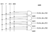
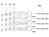
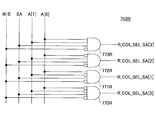
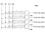
- the column decoder 225 includes a circuit 340R that decodes a column address to read data according to the first pattern, and a circuit 340W that decodes a column address to write data according to the first pattern.
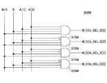
- the column decoder 225 further includes a circuit 350R that decodes a column address in order to read data according to the second pattern, and a circuit 350W that decodes a column address in order to write data according to the second pattern.
- a circuit 340R that decodes a column address to read data according to the first pattern includes four-input type AND (logical product) circuits 360R, 361R, 362R, and 363R. Four signal lines are connected to each of the AND circuits 360R to 363R.
- the first pattern selection data F, the column addresses A [1], A [0], and the write enable signal W / E are respectively connected to the AND circuits 360R to 363R. Entered.
- AND circuits 360R, 361R, 362R, and 363R output column selection data R_COL_SEL_F [0], R_COL_SEL_F [1], R_COL_SEL_F [2], and R_COL_SEL_F [3], respectively.
- the column selection data R_COL_SEL_F [0] is column selection data for selecting the bit lines BL00 and BLB00 and the bit lines BL10 and BLB10 shown in FIG. 8 in order to read data according to the first pattern.
- Column selection data R_COL_SEL_F [1] is column selection data for selecting the bit lines BL01 and BLB01 and the bit lines BL11 and BLB11 shown in FIG. 8 in order to read data according to the first pattern.
- Column selection data R_COL_SEL_F [2] is column selection data for selecting the bit lines BL02 and BLB02 and the bit lines BL12 and BLB12 shown in FIG. 8 in order to read data according to the first pattern.
- Column selection data R_COL_SEL_F [3] is column selection data for selecting the bit lines BL03 and BLB03 and the bit lines BL13 and BLB13 shown in FIG. 8 in order to read data according to the first pattern.
- the AND circuit 360R receives the first pattern selection data F, the negative column address A [1], the negative column address A [0], and the negative write enable signal W / E. .
- the AND circuit 361R receives the first pattern selection data F, the negative column address A [1], the column address A [0], and the negative write enable signal W / E.
- the AND circuit 362R receives the first pattern selection data F, the column address A [1], the negative column address A [0], and the negative operation write enable signal W / E.
- the AND circuit 363R receives the first pattern selection data F, the column address A [1], the column address A [0], and the write enable signal W / E obtained by performing a negative operation.
- the column decoder 225 determines that the first pattern selection data F is “1”, the column addresses A [1] and A [0] are “0” and “0”, and the write enable signal W / E is at the L level.
- the column selection data R_COL_SEL_F [0] is set to “1”, and the column selection data R_COL_SEL_F [1], R_COL_SEL_F [2], and R_COL_SEL_F [3] are set to “0”.
- the column decoder 225 determines that the first pattern selection data F is “1”, the column addresses A [1] and A [0] are “0” and “1”, and the write enable signal W / E is at the L level.
- the column selection data R_COL_SEL_F [1] is set to “1”
- the column selection data R_COL_SEL_F [0], R_COL_SEL_F [2], and R_COL_SEL_F [3] are set to “0”.
- the column decoder 225 determines that the first pattern selection data F is “1”, the column addresses A [1] and A [0] are “1”, “0”, and the write enable signal W / E is at the L level.
- the column selection data R_COL_SEL_F [2] is set to “1”, and the column selection data R_COL_SEL_F [0], R_COL_SEL_F [1], and R_COL_SEL_F [3] are set to “0”.
- the column decoder 225 determines that the first pattern selection data F is “1”, the column addresses A [1] and A [0] are “1”, “1”, and the write enable signal W / E is at the L level.
- the column selection data R_COL_SEL_F [3] is set to “1”, and the column selection data R_COL_SEL_F [0], R_COL_SEL_F [1], and R_COL_SEL_F [2] are set to “0”.
- a circuit 340W that decodes a column address for writing data according to the first pattern includes four-input AND (logical product) circuits 360W, 361W, 362W, and 363W. Four signal lines are connected to each of the AND circuits 360W to 363W, and the first pattern selection data F, the column addresses A [1], A [0], and the write enable signal W / E are respectively received. Entered.
- AND circuits 360W, 361W, 362W, and 363W output column selection data W_COL_SEL_F [0], W_COL_SEL_F [1], W_COL_SEL_F [2], and W_COL_SEL_F [3], respectively.
- the column selection data W_COL_SEL_F [0] is column selection data for selecting the bit lines BL00 and BLB00 and the bit lines BL10 and BLB10 shown in FIG. 8 in order to write data according to the first pattern.
- the column selection data W_COL_SEL_F [1] is column selection data for selecting the bit lines BL01 and BLB01 and the bit lines BL11 and BLB11 shown in FIG. 8 in order to write data in the first pattern.
- Column selection data W_COL_SEL_F [2] is column selection data for selecting the bit lines BL02 and BLB02 and the bit lines BL12 and BLB12 shown in FIG. 8 in order to write data in the first pattern.
- Column selection data W_COL_SEL_F [3] is column selection data for selecting the bit lines BL03 and BLB03 and the bit lines BL13 and BLB13 shown in FIG. 8 in order to write data in the first pattern.
- the AND circuit 360W receives the first pattern selection data F, the negative column address A [1], the negative column address A [0], and the write enable signal W / E.
- the AND circuit 361W receives the first pattern selection data F, the negative column address A [1], the column address A [0], and the write enable signal W / E.
- the AND circuit 362W receives the first pattern selection data F, the column address A [1], the negative column address A [0], and the write enable signal W / E.
- the first pattern selection data F, the column address A [1], the column address A [0], and the write enable signal W / E are input to the AND circuit 363W.
- the column decoder 225 determines that the first pattern selection data F is “1”, the column addresses A [1] and A [0] are “0” and “0”, and the write enable signal W / E is at the H level.
- the column selection data W_COL_SEL_F [0] is set to “1”, and the column selection data W_COL_SEL_F [1], W_COL_SEL_F [2], and W_COL_SEL_F [3] are set to “0”.
- the column decoder 225 determines that the first pattern selection data F is “1”, the column addresses A [1] and A [0] are “0” and “1”, and the write enable signal W / E is at the H level.
- the column selection data W_COL_SEL_F [1] is set to “1”
- the column selection data W_COL_SEL_F [0], W_COL_SEL_F [2], and W_COL_SEL_F [3] are set to “0”.
- the column decoder 225 determines that the first pattern selection data F is “1”, the column addresses A [1] and A [0] are “1” and “0”, and the write enable signal W / E is at the H level.
- the column selection data W_COL_SEL_F [2] is set to “1”, and the column selection data W_COL_SEL_F [0], W_COL_SEL_F [1], and W_COL_SEL_F [3] are set to “0”.
- the column decoder 225 determines that the first pattern selection data F is “1”, the column addresses A [1] and A [0] are “1”, “1”, and the write enable signal W / E is at the H level.
- the column selection data W_COL_SEL_F [3] is set to “1”, and the column selection data W_COL_SEL_F [0], W_COL_SEL_F [1], and W_COL_SEL_F [2] are set to “0”.
- a circuit 350R that decodes a column address in order to read data according to the second pattern includes 4-input type AND (logical product) circuits 370R, 371R, 372R, and 373R.
- Four signal lines are connected to each of the AND circuits 370R to 373R, and second pattern selection data S, column addresses A [1], A [0], and a write enable signal W / E are respectively received. Entered.
- AND circuits 370R, 371R, 372R, and 373R output column selection data R_COL_SEL_S [0], R_COL_SEL_S [1], R_COL_SEL_S [2], and R_COL_SEL_S [3], respectively.
- the column selection data R_COL_SEL_S [0] is column selection data for selecting the bit lines BL00 and BLB00 and the bit lines BL10 and BLB10 shown in FIG. 8 in order to read data according to the second pattern.
- Column selection data R_COL_SEL_S [1] is column selection data for selecting the bit lines BL01 and BLB01 and the bit lines BL11 and BLB11 shown in FIG. 8 in order to read data according to the second pattern.
- the column selection data R_COL_SEL_S [2] is column selection data for selecting the bit lines BL02 and BLB02 and the bit lines BL12 and BLB12 shown in FIG. 8 in order to read data according to the second pattern.
- the column selection data R_COL_SEL_S [3] is column selection data for selecting the bit lines BL03 and BLB03 and the bit lines BL13 and BLB13 shown in FIG. 8 in order to read data according to the second pattern.
- the AND circuit 370R receives the second pattern selection data S, the negative column address A [1], the negative column address A [0], and the negative write enable signal W / E. .
- the AND circuit 371R receives the second pattern selection data S, the column address A [1] obtained by the negative operation, the column address A [0], and the write enable signal W / E obtained by the negative operation.
- the AND circuit 372R receives the second pattern selection data S, the column address A [1], the negative column address A [0], and the negative operation write enable signal W / E.
- the AND circuit 373R receives the second pattern selection data S, the column address A [1], the column address A [0], and the write enable signal W / E obtained by performing a negative operation.
- the column decoder 225 determines that the second pattern selection data S is “1”, the column addresses A [1] and A [0] are “0”, “0”, and the write enable signal W / E is at the L level.
- the column selection data R_COL_SEL_S [0] is set to “1”, and the column selection data R_COL_SEL_S [1], R_COL_SEL_S [2], and R_COL_SEL_S [3] are set to “0”.
- the column decoder 225 determines that the second pattern selection data S is “1”, the column addresses A [1] and A [0] are “0” and “1”, and the write enable signal W / E is at the L level.
- the column selection data R_COL_SEL_S [1] is set to “1”
- the column selection data R_COL_SEL_S [0], R_COL_SEL_S [2], and R_COL_SEL_S [3] are set to “0”.
- the column decoder 225 determines that the second pattern selection data S is “1”, the column addresses A [1] and A [0] are “1” and “0”, and the write enable signal W / E is at the L level.
- the column selection data R_COL_SEL_S [2] is set to “1”, and the column selection data R_COL_SEL_S [0], R_COL_SEL_S [1], and R_COL_SEL_S [3] are set to “0”.
- the column decoder 225 determines that the second pattern selection data S is “1”, the column addresses A [1] and A [0] are “1”, “1”, and the write enable signal W / E is at the L level.
- the column selection data R_COL_SEL_S [3] is set to “1”, and the column selection data R_COL_SEL_S [0], R_COL_SEL_S [1], and R_COL_SEL_S [2] are set to “0”.
- a circuit 350W that decodes a column address for writing data according to the second pattern includes four-input AND (logical product) circuits 370W, 371W, 372W, and 373W.
- Four signal lines are connected to each of the AND circuits 370W to 373W, and second pattern selection data S, column addresses A [1], A [0], and a write enable signal W / E are respectively received. Entered.
- AND circuits 370W, 371W, 372W, and 373W output column selection data W_COL_SEL_S [0], W_COL_SEL_S [1], W_COL_SEL_S [2], and W_COL_SEL_S [3], respectively.
- Column selection data W_COL_SEL_S [0] is column selection data for selecting the bit lines BL00 and BLB00 and the bit lines BL10 and BLB10 shown in FIG. 8 in order to write data in the second pattern.
- the column selection data W_COL_SEL_S [1] is column selection data for selecting the bit lines BL01 and BLB01 and the bit lines BL11 and BLB11 shown in FIG. 8 in order to write data according to the second pattern.
- Column selection data W_COL_SEL_S [2] is column selection data for selecting the bit lines BL02 and BLB02 and the bit lines BL12 and BLB12 shown in FIG. 8 in order to write data in the second pattern.
- Column selection data W_COL_SEL_S [3] is column selection data for selecting the bit lines BL03 and BLB03 and the bit lines BL13 and BLB13 shown in FIG. 8 in order to write data in the second pattern.
- the AND circuit 370W receives the second pattern selection data S, the column address A [1] obtained by the negative operation, the column address A [0] obtained by the negative operation, and the write enable signal W / E.
- the AND circuit 371W receives the second pattern selection data S, the negative column address A [1], the column address A [0], and the write enable signal W / E.
- the AND circuit 372W receives the second pattern selection data S, the column address A [1], the negative column address A [0], and the write enable signal W / E.
- the second pattern selection data S, column address A [1], column address A [0], and write enable signal W / E are input to the AND circuit 373W.
- the column decoder 225 determines that the second pattern selection data S is “1”, the column addresses A [1] and A [0] are “0” and “0”, and the write enable signal W / E is at the H level.
- the column selection data W_COL_SEL_S [0] is set to “1”, and the column selection data W_COL_SEL_S [1], W_COL_SEL_S [2], and W_COL_SEL_S [3] are set to “0”.
- the column decoder 225 determines that the second pattern selection data S is “1”, the column addresses A [1] and A [0] are “0” and “1”, and the write enable signal W / E is at the H level.
- the column selection data W_COL_SEL_S [1] is set to “1”
- the column selection data W_COL_SEL_S [0], W_COL_SEL_S [2], and W_COL_SEL_S [3] are set to “0”.
- the column decoder 225 determines that the second pattern selection data S is “1”, the column addresses A [1] and A [0] are “1” and “0”, and the write enable signal W / E is at the H level.
- the column selection data W_COL_SEL_S [2] is set to “1”, and the column selection data W_COL_SEL_S [0], W_COL_SEL_S [1], and W_COL_SEL_S [3] are set to “0”.
- the column decoder 225 determines that the second pattern selection data S is “1”, the column addresses A [1] and A [0] are “1”, “1”, and the write enable signal W / E is at the H level.
- the column selection data W_COL_SEL_S [3] is set to “1”, and the column selection data W_COL_SEL_S [0], W_COL_SEL_S [1], and W_COL_SEL_S [2] are set to “0”.
- column selection data W_COL_SEL_S [0], W_COL_SEL_S [1], W_COL_SEL_S [2], And W_COL_SEL_S [3] are all “0”.
- column selection data R_COL_SEL_F [3: 0], R_COL_SEL_S [3: 0], W_COL_SEL_F [3: 0], and W_COL_SEL_S [3: 0] will be described with reference to FIG. .
- FIG. 10 is a diagram showing a connection relationship between the column selection / read / write circuit 213 of the SRAM 200 of the first embodiment and a signal line for transmitting column selection data.
- FIG. 10 four columns in the bit D [n] of the subarrays 211A and 211B are represented as C [0], C [1], C [2], and C [3]. Further, the column C [3] of the bit D [n ⁇ 1] adjacent to the bit D [n] and the column C [0] of the bit D [n + 1] are shown.
- the columns C [0] to C [3] in the subarray 211A include bit lines BL00, BLB00 to BL03, and BLB03, respectively.
- the columns C [0] to C [3] in the sub-array 211B include bit lines BL10, BLB10 to BL13, and BLB13, respectively.
- word lines WL00 to WL03 are arranged in the subarray 211A, and four wordlines WL10 to WL13 are arranged in the subarray 211B.
- One bit cell 10 is arranged at the intersection of the bit lines BL00, BLB00 to BL03, BLB03, BL10, BLB10 to BL13, BLB13 and the word lines WL00 to WL03, WL10 to WL13.
- FIG. 10 shows a total of 48 bit cells.
- a column selection / read / write circuit 213 is provided for each column.
- bit D [n] is an odd bit and the bits D [n ⁇ 1] and D [n + 1] are even bits.
- the first pattern is a pattern for reading or writing data from / to the plurality of bit cells 10 having the same address included in the odd-numbered bits in the subarray 211A and the even-numbered bits in the subarray 211B. .
- the second pattern is a pattern for reading or writing data from / to a plurality of bit cells 10 at the same address included in even-numbered bits in the sub-array 211A and odd-numbered bits in the sub-array 211B.
- R_COL_SEL_F [3: 0] R_COL_SEL_S [3: 0]
- W_COL_SEL_F W_COL_SEL_F [3: 0]
- W_COL_SEL_S W_COL_SEL_S [3: 0].
- the column selection / read / write circuit 213 sets the input destination of four types of column selection data on the upper side (Upper) or the lower side (Lower) for each bit in order to realize reading or writing of data according to the first pattern or the second pattern. ) To any one of the bits.
- column selection data for selecting the bit of the upper sub-array 211A in the sub-block 210 for data reading is represented as R_COL_SEL_U.
- column selection data for selecting the bit of the lower sub-array 211B in the sub-block 210 for data reading is represented as R_COL_SEL_L.
- column selection data for selecting the bit of the upper sub-array 211A in the sub-block 210 for data writing is represented as W_COL_SEL_U.
- column selection data for selecting a bit in the lower sub-array 211B in the sub-block 210 for data writing is represented as W_COL_SEL_L.
- the column selection data R_COL_SEL_F [3: 0] and W_COL_SEL_F [3: 0] used in the first pattern are input to the odd bits D [n] as R_COL_SEL_U and W_COL_SEL_U.
- column selection data R_COL_SEL_F [3: 0] and W_COL_SEL_F [3: 0] used in the first pattern are input as R_COL_SEL_L and W_COL_SEL_L to even bits D [n ⁇ 1] and D [n + 1].
- column selection data R_COL_SEL_S [3: 0] and W_COL_SEL_S [3: 0] used in the second pattern are input as R_COL_SEL_U and W_COL_SEL_U to even bits D [n ⁇ 1] and D [n + 1]. Is done.
- column selection data R_COL_SEL_S [3: 0] and W_COL_SEL_S [3: 0] used in the second pattern are input to the odd bits D [n] as R_COL_SEL_L and W_COL_SEL_L.
- the bits of the same address are as follows: Will be placed.
- the row selection data ROW [2] is “1” and the column selection data R_COL_SEL_F [0] is “1”. This corresponds to the case where reading is performed in the first pattern.
- bit cell 10E located at the intersection of the word line WL02 and the column C [0] is selected for the odd bit D [n]
- the word line WL12 and the column C [0] are selected for the even bit D [n + 1].
- the bit cell 10F located at the intersection is selected.
- bit cells in different subarrays (211A, 211B) have the same address. This relationship is the same for the addresses specified by the word lines WL00 to 03 and WL10 to 13 and the columns C [0] to C [3] in all bits.
- the column selection data for reading or writing data according to the first pattern and the second pattern is divided between the odd bits and the even bits as described above, so that the same between adjacent bits.
- Address bit cells are arranged in a staggered pattern.
- FIG. 11 is a diagram illustrating a circuit of the column selection / read / write circuit 213 of the SRAM 100 according to the first embodiment.
- One column selection / read / write circuit 213 is provided for each sub-block 210, and is connected to the bit lines BL and BLB of the two sub-arrays 211A and 211B in each sub-block 210.
- bit lines connected to the upper sub-array 211A in the sub-block 210 are represented as BLU and BLBU (subscript U is an abbreviation of Upper), and the bit lines connected to the lower sub-array 211B are BLL and BLBL ( The subscript L is an abbreviation for Lower).
- Bit lines BLU and BLBU correspond to, for example, bit lines BL00, BLB00 to BL03, and BL03 shown in FIG. 10, and bit lines BLL and BLBL include, for example, bit lines BL10 and BLB10 to BL13 shown in FIG. , BL13.
- the column selection data R_COL_SEL_U, R_COL_SEL_L, W_COL_SEL_U, and W_COL_SEL_L are input to the column selection / read / write circuit 213 as shown in FIG.
- the column selection / read / write circuit 213 includes NMOS transistors 381, 382, 383, 384 and an inverter 385.
- the NMOS transistors 381 and 382 receive column selection data W_COL_SEL_U at their gates, and the NMOS transistors 383 and 384 receive column selection data W_COL_SEL_L at their gates.
- the NMOS transistor 381 has a drain connected to the upper bit line BLBU and a source connected to the drain of the NMOS transistor 383.
- the NMOS transistor 383 has a source connected to the lower bit line BLBL and a drain connected to the source of the NMOS transistor 381.
- the NMOS transistor 382 has a drain connected to the upper bit line BLU and a source connected to the drain of the NMOS transistor 384.
- the NMOS transistor 384 has a source connected to the lower bit line BLL and a drain connected to the source of the NMOS transistor 382.
- connection point between the source of the NMOS transistor 381 and the drain of the NMOS transistor 383 is connected to the global bit line 214W for data writing.
- the input terminal of the inverter 385 is connected to the connection point between the source of the NMOS transistor 381 and the drain of the NMOS transistor 383, and the output terminal of the inverter 385 is connected to the connection point between the source of the NMOS transistor 382 and the drain of the NMOS transistor 384. It is connected.
- the input terminal to which the column selection data R_COL_SEL_U is input is connected to the input terminal of the inverter 387.
- the output terminal of the inverter 387 is connected to the gate of the PMOS transistor 388.
- the drain of the PMOS transistor 388 is connected to a power source of a predetermined voltage (Vdd), and the source is connected to the drain of the PMOS transistor 389.
- the gate of the PMOS transistor 389 is connected to the upper bit line BLU, and the source is connected to the drain of the PMOS transistor 390.
- the gate of the PMOS transistor 390 is connected to the lower bit line BLL, and the source is connected to the source of the PMOS transistor 391.
- the drain of the PMOS transistor 391 is connected to a power source of a predetermined voltage (Vdd), and the gate is connected to the output terminal of the inverter 392.
- the input terminal of the inverter 392 is connected to the other input terminal of the NOR circuit 386.
- connection point between the source of the PMOS transistor 389 and the drain of the PMOS transistor 390 is connected to the drain of the NMOS transistor 393 and to the gate of the NMOS transistor 394.
- the source of the NMOS transistor 393 is grounded, and the gate is connected to the output terminal of the NOR circuit 386.
- the drain of the NMOS transistor 394 is connected to the global bit line 214R for reading data, and the source is grounded.
- the NMOS transistors 381 and 382 are turned on, and the global bit line 214W for data writing and the upper bit lines BLU and BLBU are connected. As a result, data can be written to the upper bits from the global bit line 214W for data writing through the upper bit lines BLU and BLBU.
- the NMOS transistors 383 and 384 are turned on, and the global bit line 214W for data writing and the lower bit lines BLL and BLBL are connected. As a result, data can be written to the lower bits from the global bit line 214W for data writing via the lower bit lines BLL and BLBL.
- the PMOS transistor 388 is turned on, and the output of the NOR circuit 386 becomes “0”.
- the column selection data R_COL_SEL_U is “1”
- the column selection data W_COL_SEL_U is “0”
- the NMOS transistor 382 is turned off, and as a result, the PMOS transistor 389 is turned on.
- the NMOS transistor 393 is turned off and the NMOS transistor 394 is turned on.
- the upper bit line BLU and the data read global bit line 214R are connected, and the upper bit data can be read via the data read global bit line 214R.
- data can be freely read from or written to the upper or lower bit.
- FIG. 11 shows the relationship between the column selection / read / write circuit 213 arranged for one column, the global bit line 214R for reading data, and the global bit line 214W for writing data.
- the column selection / read / write circuits 213 for the other three columns not shown in FIG. 11 all have the same circuit configuration as the column selection / read / write circuit 213 shown in FIG.
- the column selection / read / write circuits 213 for the other three columns not shown in FIG. 11 are connected to the global bit line 214W for data writing via the NMOS transistors 381 to 384 and the inverter 385.
- one of the four column selection / read / write circuits 213 is turned on. It is connected to the global bit line 214W for writing data.
- the column selection / read / write circuits 213 for the other three columns not shown in FIG. 11 are connected to the data read global bit line 214R via the NMOS transistor 394.
- the NMOS transistors 381 to 384 and the NMOS transistor 394 connect any one of the four column selection / read / write circuits 213 to the global bit line 214W for data writing and the global bit line 214R for data reading.
- Switching circuits 215A and 215B (see FIG. 7).
- FIG. 12 is a diagram showing how bits are selected by the first pattern and the second pattern in the SRAM 200 of the first embodiment.
- the sub-block 210 of sub-block number 3 above the input / output port (I / O) 230A is enlarged.
- the subarray 211A and the subarray 211B include four bits D [0], D [1], D [2], and D [3], and the column selection / read / write circuit 213 is between the subarrays 211A and 211B.
- the description will be given assuming that there is something.
- the 8 bits shown in FIG. 12 each include 16 bit cells of 4 rows ⁇ 4 columns.
- bit cells are indicated by square cells.
- the four columns included in each bit D [0], D [1], D [2], D [3] are represented as C [0], C [1], C [2], C [3].
- the columns C [0] to C [3] in the subarray 211A include bit lines BL00, BLB00 to BL03, and BLB03, respectively.
- the first pattern is a pattern for reading or writing data from / to a plurality of bit cells 10 having the same address included in the odd-numbered bits in the subarray 211A and the even-numbered bits in the subarray 211B.
- one bit is skipped from the subarrays 211A and 211B and selected in a staggered manner.
- the second pattern is a pattern for reading or writing data from / to a plurality of bit cells 10 at the same address included in even-numbered bits in the sub-array 211A and odd-numbered bits in the sub-array 211B.
- one bit is skipped from the subarrays 211A and 211B and selected in a staggered manner.
- the row selection data ROW [0] output from the row decoder 221 is “1”, and the row selection data ROW [1], ROW [2], and ROW [3] are all “0”. .
- the sub block selection data SBS [3] output from the sub block decoder 222 is “1”, and the sub block selection data SBS [0], SBS [1], and SBS [2] are all “0”. It is.
- the data output from the up / down selection decoder 223 is TOP data.
- the first pattern selection data F output from the pattern selection decoder 224 is “1”, and the second pattern selection data S is “0”.
- the column selection data R_COL_SEL_F [0] output from the column decoder 225 is “1”, and the column selection data R_COL_SEL_F [1], R_COL_SEL_F [2], and R_COL_SEL_F [3] are all “0”. Note that all the column selection data R_COL_SEL_S [3: 0], W_COL_SEL_F [3: 0], and W_COL_SEL_S [3: 0] are “0”.
- the above conditions (1) to (5) are for reading data in the first pattern.
- bit cell selected in the subarray 211A is at the intersection of the column C [0] inside the odd bits D [1] and D [3] and the word line WL00, as shown by the arrows in FIG. Two bit cells.
- bit cell selected in the sub-array 211B is the intersection of the column C [0] and the word line WL10 inside the even bits D [0] and D [2] as shown by arrows in FIG. Are two bit cells.
- These four bit cells are bits of the same address specified by the first pattern, and are included one by one in four bits arranged in a staggered manner as shown in white in FIG.
- FIG. 13 is a timing chart showing an operation example of the SRAM 200 of the first embodiment.
- the four bit cells described in FIG. 12 are specified by the column C [0] and the word line WL00 for the odd bits D [1] and D [3], and the column for the even bits D [0] and D [2]. It is specified by C [0] and the word line WL10.
- the word lines WL00 and WL10 are specified by the row selection data ROW [0].
- FIG. 13 shows a system clock CLK (Clock), a read input address RA (Read (Address), row selection data ROW [0] to ROW [3], sub-block selection data SBS, and word lines WL00 to The signal levels of WL03 and WL10 to WL13 are shown.
- FIG. 13 further shows the signal level of the bit line BL00 of the bits D [1] and D [3], the signal level of the bit line BL10 of the bits D [0] and D [2], and the column selection data R_COL_SEL_F [ 0] and read data RD (Read Data).
- the system clock CLK is output from the timer 240 (see FIG. 7).
- the word lines WL00 and WL10 are selected at time t3 by the rise of the row selection data ROW [0] and the sub-block selection data SBS.
- the column selection data R_COL_SEL_F [0] rises to “1” at time t3.
- the data of the two bit cells at the intersection of the column C [0] and the word line WL00 inside the odd bits D [1] and D [3] are the bit lines BL00 of the bits D [1] and D [3], respectively. Read through.
- bit line BL10 Read through bit line BL10.
- the read data becomes RD1 at time t4.
- FIG. 14 and FIG. 15 are diagrams showing an operation example when selecting a bit cell to read data by the first pattern and the second pattern in the SRAM 200 of the first embodiment.
- even bits in the subarray 211A and odd bits in the subarray 211B selected by the second pattern are shown in gray.
- the row selection data ROW [2] is “1”, and the row selection data ROW [0], ROW [1], and ROW [3] are all “0”.
- the column selection data R_COL_SEL_F [2] is “1”, and the column selection data R_COL_SEL_F [0], R_COL_SEL_F [1], and R_COL_SEL_F [3] are all “0”.
- the data is read from the bit cell located at the intersection of the column C [2] and the word line WL02 in the odd bits D [1] and D [3], and the even bit D [0].
- the bit cell is located at the intersection of the column C [2] and the word line WL12.
- the SRAM 200 of the first embodiment has bit cells of the same address arranged in different subarrays (211A, 211B) for adjacent bits, when reading data in the first pattern, odd bits are read from the subarray 211A. Data is read and data is read from the sub-array 211B for even bits.
- row selection data ROW [0] is “1”
- row selection data ROW [1], ROW [2], and ROW [3] are all “0”.
- the column selection data R_COL_SEL_S [1] is “1”, and the column selection data R_COL_SEL_S [0], R_COL_SEL_S [2], and R_COL_SEL_S [3] are all “0”.
- bit cell located at the intersection of the column C [1] and the word line WL10 in the odd bits D [1] and D [3], and the even bit D [0].
- bit cell In D [2], the bit cell is located at the intersection of the column C [1] and the word line WL00.
- the SRAM 200 of the first embodiment has bit cells of the same address arranged in different subarrays (211A, 211B) for adjacent bits, when reading data in the second pattern, odd bits are read from the subarray 211B. Data is read and data is read from the subarray 211A for even bits.
- a plurality of bit cells having the same address are arranged in different sub-arrays for adjacent bits. That is, a plurality of bit cells having the same address are distributed in a staggered manner in a pair of subarrays 211A and 211B in one subblock 210 for adjacent bits.
- bit cells having the same address are distributed in a staggered manner by arranging the odd bits and the even bits including the bit cells having the same address in different subarrays 211A and 211B.
- the number of 1-bit columns is only four, so the reduction in operation speed due to the change in aspect ratio (horizontal length) and the lengthening of the word line is suppressed. can do.
- the first embodiment it is possible to provide a semiconductor memory device and a semiconductor memory device control method in which occurrence of data destruction over a plurality of bits is suppressed while suppressing a change in aspect ratio and a decrease in operation speed. .
- the SRAM 200 suppresses data destruction by physically changing the bit cell arrangement as described above even if data destruction corresponding to data destruction of 2 bits or more in the conventional SRAM occurs. be able to.
- FIG. 16 shows SRAM 400 of the second embodiment.
- the SRAM 400 of the second embodiment is characterized in that a plurality of bit cells having the same address are distributed in a staggered manner in sub-blocks having the same sub-block number in different sub-banks 450U and 450L for adjacent bits. Different from the SRAM 200 of the first embodiment.
- 16 includes a sub-block 210, a decoder 420, input / output ports 430A and 430B, and a timer 240.
- the sub-block 210 is arranged in four stages above and below the input / output ports 430A and 430B, as in the first embodiment. That is, FIG. 16 shows 16 sub-blocks 210.
- the sub-block numbers are assigned as 0, 1, 2, 3 from the side closer to the input / output ports 430A and 430B to the side farther from the upper and lower sides of the input / output ports 430A and 430B. This is the same as in the first embodiment.
- a set of eight sub-blocks 210 having four stages on the upper side of the input / output ports 430A and 430B is referred to as a sub bank 450U (Upper), and eight stages having four stages on the lower side of the input / output ports 430A and 430B.
- a set of sub blocks 210 is referred to as a sub bank 450L (Lower).
- Each sub-block 210 includes sub-arrays 211A and 211B and a column selection / read / write circuit 413 as in the first embodiment.
- the subarray 211A is positioned above the column selection / read / write circuit 413, and the subarray 211B is positioned below the column selection / read / write circuit 413.
- the subarrays 211A and 211B shown in FIG. 16 are bits D [n-3] to D [n].
- Each bit in each of the sub-arrays 211A and 211B includes 16 bit cells of 4 rows ⁇ 4 columns. However, for the sake of space, FIG. 16 shows 2 rows ⁇ 4 columns of the sub-arrays 211A and 211B of each bit. Bit cells are indicated by squares.
- a switching circuit 215 is shown inside the input / output port 430A of FIG. 16 in order to schematically represent data reading.
- the switching circuit 215 will be described with reference to FIG.
- the positional relationship between the sub-block 210 and the sub-arrays 211A and 211B shown in FIG. 16 represents the hierarchy of the sub-block 210 and the sub-arrays 211A and 211B, and the terms “upper” or “lower” in this specification are used. Does not represent a physical hierarchical relationship.
- FIG. 17 is a diagram illustrating the switching circuit 215 of the SRAM 400 according to the second embodiment.
- the first pattern selection data F and the second pattern selection data S are input to the switching circuit 215 from a pattern selection decoder 423 (see FIG. 18) described later.
- the switching circuit 215 is connected so that the first pattern selection data F and the second pattern selection data S are input in a staggered manner adjacent to each other.
- the four switching circuits 215 shown in FIG. 17 read or write data to or from the bit cell 10 selected from the subbank 450U or the subbank 450L for adjacent bits according to the first pattern selection data F and the second pattern selection data S. Write.
- FIG. 18 is a diagram illustrating a part of the SRAM 400 according to the second embodiment.
- FIG. 18 shows the bit D [n] portion of the sub-block 210 of two sub-block numbers 0 positioned above and below the input / output port (I / O) 430A and the input / output port (I / O) 430A.
- Two column select / read / write circuits 413, a global bit line 214, a decoder 420, and two pairs of word line drivers 412A, 412B are shown.
- the SRAM 400 reads and writes data according to a read command and a write command input from the processor core 111 (see FIG. 6).
- bit cell 10 is not shown in FIG. 18, but the subarrays 211A and 211B each include a plurality of bit cells arranged in an array.
- subarray numbers are assigned to the subarrays 211A and 211B included in each subblock 210.
- the subarrays 211A and 211B are arranged in eight stages above the input / output ports (I / O) 430A and 430B, respectively, and are arranged in eight stages below the input / output ports (I / O) 430A and 430B.
- the sub-array number is determined from the input / output port (I / O) 430A from the side closer to the input / output port (I / O) 430A with respect to the upper eight-stage sub-arrays 211A and 211B of the input / output port (I / O) 430A 0 to 7 toward the far side.
- FIG. 18 shows only the subarrays 211A and 211B of the subarray numbers 0 and 1 included in the subblock 210 of the subblock number 0 on the upper side of the input / output port (I / O) 430A for convenience of explanation. Also, only the subarrays 211A and 211B of the subarray numbers 0 and 1 included in the subblock 210 of the subblock number 0 are shown below the input / output port (I / O) 430A.
- the subarray numbers of the subarrays in the subblock 210 not shown in FIG. 18 are as follows.
- the sub-block 210 with sub-block number 1 above the input / output port (I / O) 430A shown in FIG. 16 includes a sub-array 211B with sub-array number 2 and a sub-array 211A with sub-array number 3.
- the sub-block 210 with sub-block number 2 above the input / output port (I / O) 430A includes a sub-array 211B with sub-array number 4 and a sub-array 211A with sub-array number 5.
- the sub-block 210 with sub-block number 4 above the input / output port (I / O) 430A includes a sub-array 211B with sub-array number 6 and a sub-array 211A with sub-array number 7.
- the sub-block 210 with sub-block number 1 below the input / output port (I / O) 430A shown in FIG. 16 includes a sub-array 211A with sub-array number 2 and a sub-array 211B with sub-array number 3.
- the sub-block 210 with sub-block number 2 below the input / output port (I / O) 430A includes a sub-array 211A with sub-array number 4 and a sub-array 211B with sub-array number 5.
- the sub-block 210 with sub-block number 4 below the input / output port (I / O) 430A includes a sub-array 211A with sub-array number 6 and a sub-array 211B with sub-array number 7.
- the word line drivers 412A and 412B are connected to the word lines of the subarrays 211A and 211B, respectively.
- the number of word lines is not shown, but the way of assigning the number of word lines is the same as that of the SRAM 200 of the first embodiment.
- the decoder 420 includes a row decoder 421, a sub-array decoder 422, a pattern selection decoder 423, and a column decoder 424.
- An input address is input to the decoder 420.
- a write enable signal W / E is input to the column decoder.
- the row decoder 421, the sub-array decoder 422, the pattern selection decoder 423, and the column decoder 424 are arranged one by one for the entire SRAM 400.
- the row decoder 421 and the subarray decoder 422 are connected to the word line drivers 412A and 412B via signal lines. Actually, since the sub-block 210 is hierarchized (see FIG. 7), the row decoder 421 and the sub-array decoder 422 are connected to the word line drivers 412A and 412B of all the sub-blocks 210.
- row selection by the row decoder 421, subarray selection by the subarray decoder 422, selection of the first pattern or the second pattern by the pattern selection decoder 423, and column selection by the column decoder 424 will be described.
- the row decoder 421 is connected to the word line drivers 412A and 412B via signal lines, decodes a row address included in an input address of a read command or a write command, and outputs row selection data ROW [3: 0]. Output.
- the row selection data ROW [3: 0] is input to the word line drivers 412A and 412B.
- the row decoder 421 is a decoder similar to the row decoder 221 of the first embodiment, and the row selection data ROW [3: 0] output from the row decoder 421 is also the row selection data ROW output from the row decoder 221 of the first embodiment. Same as [3: 0].
- the subarray decoder 422 is connected to the word line drivers 412A and 412B via signal lines, decodes the subarray address included in the input address of the read command or the write command, and outputs the subarray selection data SAS.
- the subscript number of the subarray selection data SAS corresponds to the subarray number (0 to 7).
- the pattern selection decoder 423 is connected to an input / output port (I / O) 430A through a signal line, and the first pattern and the second pattern are also different from the first pattern and the second pattern of the first embodiment. .
- the input / output port (I / O) 430B is not shown, but the pattern selection decoder 423 is similarly connected to the input / output port (I / O) 430B.
- the pattern selection decoder 423 decodes the pattern selection address included in the input address of the read command or the write command, and outputs the first pattern selection data F and the second pattern selection data S.
- the odd numbered bits in the subarray 211A or the subarray 211B included in the subbank 450U and the even numbered bits in the subarray 211A or the subarray 211B included in the subbank 450L is a pattern for reading or writing.
- odd-numbered bits in the sub-array 211A or sub-array 211B included in the sub-bank 450U and even-numbered bits in the sub-array 211A or sub-array 211B included in the sub-bank 450L include bit cells having the same address. To do.
- subarrays 211A or 211B selected in the subbanks 450U and 450L by the first pattern are subarrays having the same subarray number.
- even number bits in the subarray 211A or the subarray 211B included in the subbank 450U and odd number bits in the subarray 211A or the subarray 211B included in the subbank 450L is a pattern for reading or writing.
- bit cells having the same address are included in the even-numbered bits in the sub-array 211A or sub-array 211B included in the sub-bank 450U and the odd-numbered bits in the sub-array 211A or sub-array 211B included in the sub-bank 450L. To do.
- subarrays 211A or 211B selected in the subbanks 450U and 450L by the second pattern are subarrays having the same subarray number.
- bit cells having the same address are assigned to the sub-blocks 210 in the different subbanks 450U and 450L with respect to adjacent bits.
- the column decoder 424 is connected to the column selection / read / write circuit 413 through a signal line.
- the column decoder 424 receives a write enable signal W / E in addition to the column address included in the input address of the read command or write command.
- the column decoder 424 decodes the column address and outputs column selection data corresponding to the signal level of the write enable signal W / E.
- the column selection data is input to the column selection / read / write circuit 413.
- the column decoder 424 outputs column selection data R_COL_SEL [3: 0] when the signal level of the write enable signal W / E is L level.
- Column selection data R_COL_SEL [3: 0] is column selection data for selecting a column of bits in the subarrays 211A and 211B when executing data reading.
- the pair of bit lines BL and BLB of the subarray 211A or 211B is selected for reading data by the column selection data R_COL_SEL [3: 0].
- the column decoder 424 outputs the column selection data W_COL_SEL [3: 0] when the signal level of the write enable signal W / E is H level.
- Column selection data W_COL_SEL [3: 0] is column selection data for selecting a bit column in the subarrays 211A and 211B when data writing is executed.
- the pair of bit lines BL and BLB in the subarray 211A or 211B is selected for writing data by the column selection data W_COL_SEL [3: 0].
- Bit lines BL00 to BL03, BLB00 to BLB03, BL10 to BL13, and BLB10 to BLB13 are connected to the column selection / read / write circuit 413.
- the column selection / read / write circuit 413 selects a bit line based on the column selection data input from the column decoder 424.
- the column selection / read / write circuit 413 may be any circuit that can select the bit lines BL and BLB, switch between read / write, and transfer read / write data based on the column selection data input from the column decoder 424. .
- the column selection / read / write circuit 413 selects a pair of bit lines BL and BLB having the same line number for reading or writing data.
- the column selection / read / write circuit 413 is connected to a global bit line 214 that transmits read data or write data to / from the input / output ports (I / O) 430A and 430B (see FIG. 16).
- the bit line selection circuit is based on the column selection data transmitted from the column decoder 424, and includes four bit lines BL00, As long as BLB00 to BL03, BLB03, BL10, BLB10 to BL13, and BLB13 can be selected, the format is not limited.
- a circuit that transfers read data and write data can switch between read processing and write processing based on column selection data corresponding to the signal level of the write enable signal W / E. Any circuit can be used as long as it can exchange data with the global bit line 214.
- FIG. 19A shows the data structure of the input address of the SRAM 400 of the second embodiment.
- the input address A [7: 0] is 8-bit data. From the lower bit to the upper bit, the column address (column), row address (row), subarray address (SubFArray), and pattern selection address (F / S) )including.
- FIG. 19B is a diagram illustrating a circuit of the row decoder 421 of the SRAM 400 according to the second embodiment.
- the row decoder 421 includes 2-input type AND (logical product) circuits 500, 501, 502, and 503. Two signal lines are connected to each of the AND circuits 500 to 503, and row addresses A [3] and A [2] are input to the AND circuits 500 to 503, respectively.
- AND circuits 500, 501, 502, and 503 output row selection data R [0], R [1], R [2], and R [3], respectively.
- the row decoder 421 is a decoder similar to the row decoder 221 of the first embodiment.
- FIG. 19C is a diagram illustrating a circuit of the subarray decoder 422 of the SRAM 400 according to the second embodiment.
- the sub-array decoder 422 includes three-input type AND (logical product) circuits 510, 511, 512, 513, 514, 515, 516, and 517. Each of the AND circuits 510 to 517 is connected to three signal lines, to which subarray addresses A [6], A [5], and A [4] are input, respectively.
- the AND circuits 510, 511, 512, 513, 514, 515, 516, and 517 have subarray selection data SAS [0], SAS [1], SAS [2], SAS [3], SAS [4], and SAS, respectively. [5], SAS [6], SAS [7] are output.
- the subarray selection data SAS [0] is subarray selection data for selecting the subarray 211A (SubAArray 0) having the subarray number 0.
- the sub-array selection data SAS [0] is sub-array selection data for simultaneously selecting the sub-array 211A having sub-array number 0 included in each of the sub-banks 450U and 450L.
- the subarray selection data SAS [1] to SAS [7] are subarray selection data for selecting the subarrays 211A or 211B of the subarray numbers 1 to 7, respectively.
- the subarray selection data SAS [1] to SAS [7] are subarray selection data for simultaneously selecting the subarrays 211A or 211B having the subarray number included in each of the subbanks 450U and 450L.
- the AND block 510 receives all of the sub-block selection addresses A [6], A [5], and A [4] after performing a negative operation.
- the sub block selection addresses A [6] and A [5] are subjected to a negative operation and input, and the sub block selection address A [4] is input as it is.
- the sub-block selection addresses A [6] and A [4] are subjected to a negative operation and input, and the sub-block selection address A [5] is input as it is.
- the sub block selection address A [6] is subjected to a negative operation and inputted, and the sub block selection addresses A [5] and A [4] are inputted as they are.
- the AND block 514 receives the sub-block selection address A [6] as it is and inputs the sub-block selection addresses A [5] and A [4] after performing a negative operation.
- the sub-block selection addresses A [6] and A [4] are input as they are, and the sub-block selection address A [5] is negatively input.
- the subblock selection addresses A [6] and A [5] are input as they are, and the subblock selection address A [4] is input after being subjected to a negative operation.
- the sub-block selection addresses A [6], A [5], and A [4] are all input to the AND circuit 517 as they are.
- the subarray decoder 422 sets the subarray selection data SAS [0] to “1” when the subblock selection addresses A [6], A [5], and A [4] are “0”, “0”, and “0”.
- the subarray selection data SAS [1] to SAS [7] are set to “0”.
- the subarray decoder 422 sets the subarray selection data SAS [1] to “1” when the subblock selection addresses A [6], A [5], and A [4] are “0”, “0”, and “1”.
- the subarray selection data SAS [0], SAS [2] to SAS [7] are set to “0”.
- the subarray decoder 422 sets the subarray selection data SAS [2] to “1” when the subblock selection addresses A [6], A [5], and A [4] are “0”, “1”, and “0”.
- the subarray selection data SAS [0], SAS [1], SAS [3] to SAS [7] are set to “0”.
- the subarray decoder 422 sets the subarray selection data SAS [3] to “1” when the subblock selection addresses A [6], A [5], and A [4] are “0”, “1”, and “1”. Then, the sub-array selection data SAS [0] to SAS [2] and SAS [4] to SAS [7] are set to “0”.
- the subarray decoder 422 sets the subarray selection data SAS [4] to “1” when the subblock selection addresses A [6], A [5], and A [4] are “1”, “0”, and “0”.
- the subarray selection data SAS [0] to SAS [3] and SAS [5] to SAS [7] are set to “0”.
- the subarray decoder 422 sets the subarray selection data SAS [5] to “1” when the subblock selection addresses A [6], A [5], and A [4] are “1”, “0”, and “1”.
- the subarray selection data SAS [0] to SAS [4], SAS [6], and SAS [7] are set to “0”.
- the subarray decoder 422 sets the subarray selection data SAS [6] to “1” when the subblock selection addresses A [6], A [5], and A [4] are “1”, “1”, and “0”.
- the subarray selection data SAS [0] to SAS [5] and SAS [7] are set to “0”.
- the subarray decoder 422 sets the subarray selection data SAS [7] to “1” when the subblock selection addresses A [6], A [5], and A [4] are “1”, “1”, and “1”.
- the subarray selection data SAS [0] to SAS [6] are set to “0”.
- FIG. 19D is a diagram illustrating a circuit of the pattern selection decoder 423 of the SRAM 400 according to the second embodiment.
- the pattern selection decoder 423 has a 1-input / 2-output circuit, decodes the pattern selection address A [7], and outputs first pattern selection data F and second pattern selection data S.
- the first pattern selection data F is output as an inverted value of the data value of the pattern selection address A [7] by the inverter 520, and the second pattern selection data S is output as the data value of the pattern selection address A [7].
- the first pattern selection data F and the second pattern selection data S are data for selecting the first pattern or the second pattern, and are input to the input / output ports (I / O) 430A and 430B.
- FIG. 19E is a diagram illustrating a circuit of the column decoder 424 of the SRAM 400 according to the second embodiment.
- the column decoder 424 includes 2-input type AND (logical product) circuits 530, 531, 532, and 533. Two signal lines are connected to each of the AND circuits 530 to 533, and column addresses A [1] and A [0] are input to the AND circuits 530 to 533, respectively.
- AND circuits 530, 531, 532, and 533 output column selection data R_COL_SEL [0], R_COL_SEL [1], R_COL_SEL [2], and R_COL_SEL [3], respectively.
- the input / output ports (I / O) 430A and 430B have the first pattern or the second pattern, and the global bit line 214
- the data to be read from each bit or the data to be written to each bit is selected via.
- bit cells with the same address are assigned to the sub-blocks 210 in the different subbanks 450U and 450L for adjacent bits.
- the plurality of bit cells having the same address in the SRAM 400 of the second embodiment are distributed in a zigzag manner by assigning adjacent bits to the sub-blocks 210U and the sub-blocks 210 in the sub-bank 450L.
- FIG. 20 and FIG. 21 are diagrams showing the sub-blocks including the bit cells of the same address in the SRAM 400 of the second embodiment in different colors.
- sub-blocks 210 having sub-block numbers 0 to 3 for bits D [0] to D [7] included in sub-banks 450U and 450L are represented by squares.
- reference numeral 210 is shown only for the sub-block of sub-block number 3 of bit D [0], but each cell represents a sub-block (see FIGS. 16 and 18). The subarrays and bit cells in each subblock 210 are not shown.
- an input / output port 430A is shown between the subbank 450U and the subbank 450L.
- the input / output port 430A includes a switching circuit 215.
- a square sub-block 210 shown in white is a sub-block including a sub-array 211A or 211B (see FIGS. 16 and 18) where data is read or written according to the first pattern.
- bit cells having the same column number and row number are bit cells having the same address.
- bit cells from which data is read or written in the first pattern are assigned to subbank 450U for odd bits and to subbank 450L for even bits. Assigned.
- the gray sub-block 210 shown in gray is a sub-block including a sub-array 211A or 211B (see FIGS. 16 and 18) where data is read or written according to the second pattern.
- bit cells having the same column number and row number are bit cells having the same address.
- bit cells from / to which data is read or written in the second pattern are assigned to subbank 450U for even bits and to subbank 450L for odd bits. Assigned.
- FIG. 21 shows the flow of data when subarray selection data SAS [2] or SAS [3] is “1” and data is read out from the subblock of subblock number 1 in the second pattern. Represented by
- a plurality of bit cells having the same address are allocated to sub-blocks 210U and sub-blocks 210 in different sub-banks 450L with respect to adjacent bits, and are distributed in a staggered manner.
- the number of 1-bit columns is only four, so the reduction in operation speed due to the change in aspect ratio (horizontal length) and the lengthening of the word line is suppressed. can do.
- the second embodiment it is possible to provide a semiconductor memory device and a method for controlling the semiconductor memory device in which occurrence of data destruction over a plurality of bits is suppressed while suppressing a change in aspect ratio and a decrease in operation speed. .
- FIG. 22 shows an SRAM 600 according to the third embodiment.
- the SRAM 600 of the third embodiment is a combination of the distribution of the plurality of bit cells having the same address in the SRAM 200 of the first embodiment and the distribution of the plurality of bit cells having the same address in the SRAM 400 of the second embodiment.
- a sub-block 210 includes a decoder 620, input / output ports 430A and 430B, and a timer 240.
- FIG. 22 shows four bits (D [n], D [n-1], D [n-2], D [n-3]) in the sub-block 210 of the SRAM 600.
- Bit D [n] is assumed to be an odd number of bits.
- each bit of the sub-arrays 211A and 211B in each sub-block 210 includes 16 bit cells 10 of 4 rows ⁇ 4 columns.
- FIG. 22 shows sub-arrays 211A and 211B of each bit.
- Bit cells for 2 rows ⁇ 4 columns are indicated by squares.
- bit cells in bits D [n ⁇ 3] to D [n] are color-coded in white and gray, and are distinguished by the presence or absence of a cross, but the bit cells in the bits not shown in FIG.
- groups of 4 bits are grouped according to white / gray color classification and presence / absence of x mark. This grouping will be described later.
- the positional relationship between the sub-block 210 and the sub-arrays 211A and 211B shown in FIG. 22 represents the hierarchical structure of the sub-block 210 and the sub-arrays 211A and 211B, and the terms “upper” or “lower” in this specification are used. Does not represent a physical hierarchical relationship.
- FIG. 23 is a diagram illustrating a part of the SRAM 600 according to the third embodiment.
- bits D [n] and D [D] of the sub-block 210 of two sub-block numbers 0 positioned above and below the input / output port (I / O) 430A and the input / output port (I / O) 430A are shown.
- n-1] two column selection / read / write circuits 213, a global bit line 214, a decoder 420, and two pairs of word line drivers 212A and 212B.
- bit D [n] is an odd bit and bit [n ⁇ 1] is an even bit.
- n of bit D [n] is referred to as a bit number.
- the SRAM 600 reads and writes data according to a read command and a write command input from the processor core 111 (see FIG. 6).
- each of the subarrays 211A and 211B includes a plurality of bit cells arranged in an array.
- the sub-block 210 includes sub-arrays 211A and 211B, word line drivers 212A and 212B, and a column selection / read / write circuit 213.
- the arrangement and subarray number of the subarrays 211A and 211B are the same as those of the SRAM 400 of the second embodiment.
- the word line drivers 212A and 212B are provided corresponding to the sub arrays 211A and 211B, respectively, and are connected to the word lines included in the sub arrays 211A and 211B, respectively.
- the word line drivers 212A and 212B perform row selection (word line selection) based on row selection data (row selection signal) output by the decoder 220 decoding and outputting a row address, respectively.
- the column selection / read / write circuit 213 is provided corresponding to each sub-block 210 and is connected to the bit lines of the two sub-arrays 211A and 211B in each sub-block 210.
- the column selection / read / write circuit 213 performs column selection (bit line selection) based on column selection data (column selection signal) output by the decoder 220 decoding and outputting a column address.
- the decoder 620 includes a row decoder 221, a sub-block decoder 222, a pattern selection decoder 623, a region selection decoder 624, and a column decoder 625.
- An input address is input to the decoder 620.
- the column decoder 625 receives a write enable signal W / E.
- the decoder 620 incorporates a pattern selection decoder 623 instead of the up / down selection decoder 223 of the decoder 220 of the first embodiment, incorporates an area selection decoder 624 instead of the pattern selection decoder 224, and replaces the column decoder 225 with a column decoder. 625 is incorporated.
- the row decoder 221 and the sub block decoder 222 are the same as the row decoder 221 and the sub block decoder 222 of the first embodiment.
- the pattern selection decoder 623 is a decoder for selecting the first pattern and the second pattern, and is the same as the pattern selection decoder 224 of the first embodiment, but the first pattern selection data F (First) and the second pattern A signal line for outputting the selection data S (Second) is connected to input / output ports (I / O) 430A and 430B.
- the pattern selection decoder 623 decodes the pattern selection address included in the input address of the read command or the write command and outputs the first pattern selection data F and the second pattern selection data S.
- the first pattern selection data F and the second pattern selection data S are data for selecting the first pattern or the second pattern, respectively.
- the first pattern selection data F is input to the input / output port (I / O) 430A of the odd bit D [n], and the second pattern selection data S is input / output port (I of the even bit D [n-1]). / O) is input to 430A.
- data is read or written to odd bits of the subbank 450U, and data is read or written to even bits of the subbank 450L.
- data is read from or written to even bits in the subbank 450U, and data is read from or written to odd bits in the subbank 450L.
- the region selection decoder 624 selects bits from the upper sub-array 211A and the lower sub-array 211B included in one sub-block 210.
- the region selection decoder 624 selects odd bits of the subarray 211A and even bits adjacent to the odd bits as the first region.
- the odd bits and the even bits included in the first area have bit numbers that are even for younger bits than for odd bits.
- the area selection decoder 624 selects the odd bits of the subarray 211B and the even bits adjacent to the odd bits as the second area. For example, the odd number bits and the even number bits included in the second region are assumed to have a bit number smaller in the even number bits than in the odd number bits.
- bit numbers of all the bits included in the first area are different from the bit numbers of all the bits included in the second area.
- bit numbers of the bits included in the first area are missing by two, for example, 0, 1, 4, 5, 8, 9, 12, 13,.
- bit numbers of the bits included in the second area are missing by two, for example, 2, 3, 6, 7, 10, 11, 14, 15.
- the first region is a region including bits shown in white in FIG. 22, and the second region is a region including bits shown in gray in FIG.
- the area selection decoder 624 selects the bits of the subarrays 211A and 211B in each subblock 210 in a zigzag pattern by two bits, and thereby divides them into a white first area and a gray second area as shown in FIG. It is done.
- the area selection decoder 624 decodes the area selection address included in the input address to select the first area or the second area, and the first area selection data FA (First (Area) or the second area selection data SA ( Second Area) is output.
- the column decoder 625 is connected to the column selection / read / write circuit 213 through a signal line.
- the column decoder 625 is actually connected to the column selection / read / write circuit 213 in all the sub-blocks 210 shown in FIG.
- the column decoder 625 receives the first area selection data FA, the second area selection data SA, and the write enable signal W / E in addition to the column address included in the input address of the read command or the write command.
- the column decoder 625 decodes the column address and outputs column selection data corresponding to the data values of the first area selection data FA and the second area selection data SA and the signal level of the write enable signal W / E.
- the column selection data output from the column decoder 625 is data for selecting a column in the bits of the subarrays 211A and 211B so as to realize reading or writing of data in the first area or the second area.
- Column selection data is input to the column selection / read / write circuit 213.
- the column decoder 625 when the signal level of the write enable signal W / E is L level, the first area selection data FA is “1”, and the second area selection data SA is “0”, the column selection data.
- R_COL_SEL_FA [3: 0] is output.
- Column selection data R_COL_SEL_FA [3: 0] is column selection data for selecting a column of bits in the subarrays 211A and 211B in order to realize data reading in the first area.
- the column selection data R_COL_SEL_FA [3: 0] selects one of the bit line BL and BLB pairs of bits in the first area of the subarrays 211A and 211B for data reading.
- the column decoder 625 when the signal level of the write enable signal W / E is L level, the first area selection data FA is “0”, and the second area selection data SA is “1”, the column selection data.
- R_COL_SEL_SA [3: 0] is output.
- the column selection data R_COL_SEL_SA [3: 0] is column selection data for selecting a bit column in the subarrays 211A and 211B in order to realize data reading in the second area.
- the column decoder 625 determines that the column enable column W / E is H level, the first area selection data FA is “1”, and the second area selection data SA is “0”. Selection data W_COL_SEL_FA [3: 0] is output.
- Column selection data W_COL_SEL_FA [3: 0] is column selection data for selecting a column of bits in the subarrays 211A and 211B in order to realize data writing in the first area.
- the column selection data W_COL_SEL_FA [3: 0] selects a pair of bit lines BL and BLB of one of the bits in the first area of the subarrays 211A and 211B for data writing.
- the column decoder 625 determines that if the signal level of the write enable signal W / E is H level, the first area selection data FA is “0”, and the second area selection data SA is “1”, Selection data W_COL_SEL_SA [3: 0] is output.
- Column selection data W_COL_SEL_SA [3: 0] is column selection data for selecting a bit column in the subarrays 211A and 211B in order to realize data writing in the second area.
- the column selection data W_COL_SEL_SA [3: 0] selects a pair of bit lines BL and BLB of one of the bits in the second area of the subarrays 211A and 211B for data writing.
- column selection data R_COL_SEL_FA [3: 0], R_COL_SEL_SA [3: 0], W_COL_SEL_FA [3: 0], and W_COL_SEL_SA [3: 0] are notations that collectively represent 4-bit column selection data. .
- the column selection data R_COL_SEL_FA [3: 0] includes column selection data R_COL_SEL_FA [3], R_COL_SEL_FA [2], R_COL_SEL_FA [1], and R_COL_SEL_FA [0].
- the pattern selection decoder 623 selects the first pattern or the second pattern
- the area selection decoder 624 selects the first area or the second area.
- either the first pattern or the second pattern is selected for adjacent bits, so that the upper sub-bank of the input / output port (I / O) 430A is selected.
- 450U or the lower sub-bank 450L is specified in a staggered pattern. This is the state indicated by the presence or absence of x in FIG.
- bits including bit cells are selected in a zigzag manner by 2 bits for each of the subarrays 211A and 211B in each subblock 210.
- the This is the state shown in white / gray in FIG.
- the bit cell of the same address is represented by a white bit with an X mark, a white bit without an X mark, a gray bit with an X mark, and a gray bit without an X mark. It is divided so as to belong to one of the four groups.
- bit cells with the same column number and row number are bit cells with the same address.
- FIG. 24A shows the data structure of the input address of the SRAM 600 of the third embodiment.
- the input address A [7: 0] is 8-bit data. From the lower bit to the upper bit, the column address (column), row address (row), area selection address (FA / SA), sub block address (Sub Block ), Pattern selection address (F / S).
- the column address (column) is 2 bits of A [1: 0]
- the row address (row) is 2 bits of A [3: 2]
- the area selection address (FA / SA) is 1 of A [4].
- Two bits of A [6: 5] are assigned to the bit and sub-block address (Sub Block), and one bit of A [7] is assigned to the pattern selection address (F / S).
- FIG. 24B shows a circuit of the row decoder 221 of the SRAM 600 according to the third embodiment.
- the row decoder 221 includes two-input type AND (logical product) circuits 300, 301, 302, and 303. Two signal lines are connected to each of the AND circuits 300 to 303, and row addresses A [3] and A [2] are input thereto, respectively.
- AND circuits 300, 301, 302, and 303 output row selection data R [0], R [1], R [2], and R [3], respectively.
- the row decoder 221 is the same as the row decoder 221 of the first embodiment.
- FIG. 24C shows a circuit of the sub-block decoder 222 of the SRAM 600 according to the third embodiment.
- the sub-block decoder 222 is the same as the sub-block decoder 222 of the first embodiment, and outputs the sub-block selection data SBS [0], SBS [1], SBS [2], SBS [3].
- FIG. 24D shows a circuit of the pattern selection decoder 623 of the SRAM 600 according to the third embodiment.
- the pattern selection decoder 623 has a 1-input / 2-output circuit, decodes the pattern selection address A [7], and outputs first pattern selection data F and second pattern selection data S.
- the second pattern selection data is output as an inverted value of the data value of the pattern selection address A [7] by the inverter 720, and the first pattern selection data F is output as the data value of the pattern selection address A [7].
- the first pattern selection data F is “1” and the second pattern selection data S is “0”, the first pattern is selected. Conversely, when the first pattern selection data F is “0” and the second pattern selection data S is “1”, the second pattern is selected.
- FIG. 24E is a diagram showing a circuit of the area selection decoder 624 of the SRAM 600 according to the third embodiment.
- the area selection decoder 624 has a 1-input / 2-output type circuit, decodes the area selection address A [4], and outputs the first area selection data FA and the second area selection data SA.
- the first area selection data FA is output as an inverted value of the data value of the area selection address A [4] by the inverter 730, and the second area selection data SA is output as the data value of the area selection address A [4].
- the first area selection data FA and the second area selection data SA are data for selecting the first area or the second area, and are input to the column decoder 225.
- the column decoder 625 decodes the column address and outputs column selection data corresponding to the data values of the first area selection data FA and the second area selection data SA and the signal level of the write enable signal W / E.
- FIGS. 24F to 24I are diagrams showing a circuit for decoding a column address included in the column decoder 625 of the SRAM 600 according to the third embodiment.
- the column decoder 625 includes a circuit 740R that decodes a column address in order to read data in the first area, and a circuit 740W that decodes a column address in order to write data in the first area.
- the column decoder 625 further includes a circuit 750R for decoding the column address for reading data in the second area, and a circuit 750W for decoding the column address for writing data in the second area.
- a circuit 740R that decodes a column address to read data in the first area includes 4-input AND circuits 760R, 761R, 762R, and 763R.
- Four signal lines are connected to each of the AND circuits 760R to 763R, and the first area selection data FA, the column addresses A [1], A [0], and the write enable signal W / E are respectively received. Entered.
- AND circuits 760R, 761R, 762R, and 763R output column selection data R_COL_SEL_FA [0], R_COL_SEL_FA [1], R_COL_SEL_FA [2], and R_COL_SEL_FA [3], respectively.
- Column selection data R_COL_SEL_FA [0] is column selection data for selecting bit lines BL00 and BLB00 and bit lines BL10 and BLB10 shown in FIG. 23 in order to read data in the first area.
- Column selection data R_COL_SEL_FA [1] is column selection data for selecting bit lines BL01 and BLB01 and bit lines BL11 and BLB11 shown in FIG. 23 in order to read data in the first area.
- the column selection data R_COL_SEL_FA [2] is column selection data for selecting the bit lines BL02 and BLB02 and the bit lines BL12 and BLB12 shown in FIG. 23 in order to read data in the first area.
- Column selection data R_COL_SEL_FA [3] is column selection data for selecting the bit lines BL03 and BLB03 and the bit lines BL13 and BLB13 shown in FIG. 23 in order to read data in the first area.
- the AND circuit 760R receives the first area selection data FA, the negative column address A [1], the negative column address A [0], and the negative write enable signal W / E. .
- the AND circuit 761R receives the first area selection data FA, the negative column address A [1], the column address A [0], and the negative write enable signal W / E.
- the AND circuit 762R receives the first area selection data FA, the column address A [1], the negative column address A [0], and the negative operation write enable signal W / E.
- the AND circuit 763R receives the first area selection data FA, the column address A [1], the column address A [0], and the write enable signal W / E obtained by performing a negative operation.
- the column decoder 625 determines that the first area selection data FA is “1”, the column addresses A [1] and A [0] are “0” and “0”, and the write enable signal W / E is at the L level.
- the column selection data R_COL_SEL_FA [0] is set to “1”
- the column selection data R_COL_SEL_FA [1], R_COL_SEL_FA [2], and R_COL_SEL_FA [3] are set to “0”.
- the column decoder 625 determines that the first area selection data FA is “1”, the column addresses A [1] and A [0] are “0” and “1”, and the write enable signal W / E is at the L level.
- the column selection data R_COL_SEL_FA [1] is set to “1”
- the column selection data R_COL_SEL_FA [0], R_COL_SEL_FA [2], and R_COL_SEL_FA [3] are set to “0”.
- the column decoder 625 determines that the first area selection data FA is “1”, the column addresses A [1] and A [0] are “1” and “0”, and the write enable signal W / E is at the L level.
- the column selection data R_COL_SEL_FA [2] is set to “1”, and the column selection data R_COL_SEL_FA [0], R_COL_SEL_FA [1], and R_COL_SEL_FA [3] are set to “0”.
- the column decoder 625 determines that the first area selection data FA is “1”, the column addresses A [1] and A [0] are “1”, “1”, and the write enable signal W / E is at the L level.
- the column selection data R_COL_SEL_FA [3] is set to “1”, and the column selection data R_COL_SEL_FA [0], R_COL_SEL_FA [1], and R_COL_SEL_FA [2] are set to “0”.
- a circuit 740W that decodes a column address to write data in the first area includes four-input AND (logical product) circuits 760W, 761W, 762W, and 763W.
- Four signal lines are connected to each of the AND circuits 760W to 763W, and the first area selection data FA, the column addresses A [1], A [0], and the write enable signal W / E are respectively received. Entered.
- AND circuits 760W, 761W, 762W, and 763W output column selection data W_COL_SEL_FA [0], W_COL_SEL_FA [1], W_COL_SEL_FA [2], and W_COL_SEL_FA [3], respectively.
- Column selection data W_COL_SEL_FA [0] is column selection data for selecting bit lines BL00 and BLB00 and bit lines BL10 and BLB10 shown in FIG. 23 in order to write data in the first area.
- Column selection data W_COL_SEL_FA [1] is column selection data for selecting bit lines BL01 and BLB01 and bit lines BL11 and BLB11 shown in FIG. 23 in order to write data in the first area.
- Column selection data W_COL_SEL_FA [2] is column selection data for selecting bit lines BL02 and BLB02 and bit lines BL12 and BLB12 shown in FIG. 23 in order to write data in the first area.
- Column selection data W_COL_SEL_FA [3] is column selection data for selecting the bit lines BL03 and BLB03 and the bit lines BL13 and BLB13 shown in FIG. 23 in order to write data in the first area.
- the AND circuit 760W receives the first area selection data FA, the negative column address A [1], the negative column address A [0], and the write enable signal W / E.
- the AND circuit 761W receives the first area selection data FA, the negative column address A [1], the column address A [0], and the write enable signal W / E.
- the AND circuit 762W receives the first area selection data FA, the column address A [1], the negative column address A [0], and the write enable signal W / E.
- the first area selection data FA, the column address A [1], the column address A [0], and the write enable signal W / E are input to the AND circuit 763W.
- the column decoder 625 determines that the first area selection data FA is “1”, the column addresses A [1] and A [0] are “0” and “0”, and the write enable signal W / E is at the H level.
- the column selection data W_COL_SEL_FA [0] is set to “1”
- the column selection data W_COL_SEL_FA [1], W_COL_SEL_FA [2], and W_COL_SEL_FA [3] are set to “0”.
- the column decoder 625 determines that the first area selection data FA is “1”, the column addresses A [1] and A [0] are “0”, “1”, and the write enable signal W / E is at the H level.
- the column selection data W_COL_SEL_FA [1] is set to “1”
- the column selection data W_COL_SEL_FA [0], W_COL_SEL_FA [2], and W_COL_SEL_FA [3] are set to “0”.
- the column decoder 625 determines that the first area selection data FA is “1”, the column addresses A [1] and A [0] are “1” and “0”, and the write enable signal W / E is at the H level.
- the column selection data W_COL_SEL_FA [2] is set to “1”, and the column selection data W_COL_SEL_FA [0], W_COL_SEL_FA [1], and W_COL_SEL_FA [3] are set to “0”.
- the column decoder 625 determines that the first area selection data FA is “1”, the column addresses A [1] and A [0] are “1”, “1”, and the write enable signal W / E is at the H level.
- the column selection data W_COL_SEL_FA [3] is set to “1”, and the column selection data W_COL_SEL_FA [0], W_COL_SEL_FA [1], and W_COL_SEL_FA [2] are set to “0”.
- a circuit 750R that decodes a column address for reading data in the second area includes four-input AND (logical product) circuits 770R, 771R, 772R, and 773R.
- Four signal lines are connected to each of the AND circuits 770R to 773R, and second area selection data SA, column addresses A [1], A [0], and a write enable signal W / E are respectively received. Entered.
- AND circuits 770R, 771R, 772R, and 773R output column selection data R_COL_SEL_SA [0], R_COL_SEL_SA [1], R_COL_SEL_SA [2], and R_COL_SEL_SA [3], respectively.
- Column selection data R_COL_SEL_SA [0] is column selection data for selecting bit lines BL00 and BLB00 and bit lines BL10 and BLB10 shown in FIG. 23 in order to read data in the second area.
- Column selection data R_COL_SEL_SA [1] is column selection data for selecting the bit lines BL01 and BLB01 and the bit lines BL11 and BLB11 shown in FIG. 23 in order to read data in the second area.
- Column selection data R_COL_SEL_SA [2] is column selection data for selecting bit lines BL02 and BLB02 and bit lines BL12 and BLB12 shown in FIG. 23 in order to read data in the second area.
- Column selection data R_COL_SEL_SA [3] is column selection data for selecting bit lines BL03 and BLB03 and bit lines BL13 and BLB13 shown in FIG. 23 in order to read data in the second area.
- the AND circuit 770R receives the second area selection data SA, the negative column address A [1], the negative column address A [0], and the negative write enable signal W / E. .
- the AND circuit 771R receives the second area selection data SA, the column address A [1] obtained by the negative operation, the column address A [0], and the write enable signal W / E obtained by the negative operation.
- the AND circuit 772R receives the second area selection data SA, the column address A [1], the negative column address A [0], and the negative operation write enable signal W / E.
- the AND circuit 773R receives the second area selection data SA, the column address A [1], the column address A [0], and the write enable signal W / E obtained by performing a negative operation.
- the column decoder 625 determines that the second area selection data SA is “1”, the column addresses A [1] and A [0] are “0” and “0”, and the write enable signal W / E is at the L level.
- the column selection data R_COL_SEL_SA [0] is set to “1”
- the column selection data R_COL_SEL_SA [1], R_COL_SEL_SA [2], and R_COL_SEL_SA [3] are set to “0”.
- the column decoder 625 determines that the second area selection data SA is “1”, the column addresses A [1] and A [0] are “0” and “1”, and the write enable signal W / E is at the L level.
- the column selection data R_COL_SEL_SA [1] is set to “1”
- the column selection data R_COL_SEL_SA [0], R_COL_SEL_SA [2], and R_COL_SEL_SA [3] are set to “0”.
- the column decoder 625 determines that the second area selection data SA is “1”, the column addresses A [1] and A [0] are “1” and “0”, and the write enable signal W / E is at the L level.
- the column selection data R_COL_SEL_SA [2] is set to “1”
- the column selection data R_COL_SEL_SA [0], R_COL_SEL_SA [1], and R_COL_SEL_SA [3] are set to “0”.
- the column decoder 625 determines that the second area selection data SA is “1”, the column addresses A [1] and A [0] are “1” and “1”, and the write enable signal W / E is at the L level.
- the column selection data R_COL_SEL_SA [3] is set to “1”, and the column selection data R_COL_SEL_SA [0], R_COL_SEL_SA [1], and R_COL_SEL_SA [2] are set to “0”.
- a circuit 750W that decodes a column address to write data in the second area includes four-input AND (logical product) circuits 770W, 771W, 772W, and 773W.
- Four signal lines are connected to each of the AND circuits 770W to 773W, and second area selection data SA, column addresses A [1], A [0], and a write enable signal W / E are respectively received. Entered.
- AND circuits 770W, 771W, 772W, and 773W output column selection data W_COL_SEL_SA [0], W_COL_SEL_SA [1], W_COL_SEL_SA [2], and W_COL_SEL_SA [3], respectively.
- Column selection data W_COL_SEL_SA [0] is column selection data for selecting the bit lines BL00 and BLB00 and the bit lines BL10 and BLB10 shown in FIG. 23 in order to write data in the second area.
- Column selection data W_COL_SEL_SA [1] is column selection data for selecting the bit lines BL01 and BLB01 and the bit lines BL11 and BLB11 shown in FIG. 23 in order to write data in the second area.
- Column selection data W_COL_SEL_SA [2] is column selection data for selecting bit lines BL02 and BLB02 and bit lines BL12 and BLB12 shown in FIG. 23 in order to write data in the second area.
- Column selection data W_COL_SEL_SA [3] is column selection data for selecting the bit lines BL03 and BLB03 and the bit lines BL13 and BLB13 shown in FIG. 23 in order to write data in the second area.
- the AND circuit 770W receives the second area selection data SA, the column address A [1] subjected to the negative operation, the column address A [0] subjected to the negative operation, and the write enable signal W / E.
- the AND circuit 771W receives the second area selection data SA, the column address A [1] obtained by the negative operation, the column address A [0], and the write enable signal W / E.
- the AND circuit 772W receives the second area selection data SA, the column address A [1], the negative column address A [0], and the write enable signal W / E.
- the second area selection data SA, column address A [1], column address A [0], and write enable signal W / E are input to the AND circuit 773W.
- the column decoder 625 determines that the second area selection data SA is “1”, the column addresses A [1] and A [0] are “0” and “0”, and the write enable signal W / E is at the H level.
- the column selection data W_COL_SEL_SA [0] is set to “1”
- the column selection data W_COL_SEL_SA [1], W_COL_SEL_SA [2], and W_COL_SEL_SA [3] are set to “0”.
- the column decoder 625 determines that the second area selection data SA is “1”, the column addresses A [1], A [0] are “0”, “1”, and the write enable signal W / E is at the H level.
- the column selection data W_COL_SEL_SA [1] is set to “1”
- the column selection data W_COL_SEL_SA [0], W_COL_SEL_SA [2], and W_COL_SEL_SA [3] are set to “0”.
- the column decoder 625 determines that the second area selection data SA is “1”, the column addresses A [1] and A [0] are “1” and “0”, and the write enable signal W / E is at the H level.
- the column selection data W_COL_SEL_SA [2] is set to “1”
- the column selection data W_COL_SEL_SA [0], W_COL_SEL_SA [1], and W_COL_SEL_SA [3] are set to “0”.
- the column decoder 625 determines that the second area selection data SA is “1”, the column addresses A [1] and A [0] are “1”, “1”, and the write enable signal W / E is at the H level.
- the column selection data W_COL_SEL_SA [3] is set to “1”, and the column selection data W_COL_SEL_SA [0], W_COL_SEL_SA [1], and W_COL_SEL_SA [2] are set to “0”.
- the input / output ports 430A and 430B are the same as the input / output ports 430A and 430B of the second embodiment. Based on the first pattern selection data F or the second pattern selection data S, the input / output ports 430A and 430B are global in the first pattern or the second pattern. Data to be read from each bit or data to be written to each bit is selected via the bit line 214.
- Both the first pattern selection data F and the second pattern selection data S are input to the input / output port (I / O) 430A of the odd bits D [n] and even bits D [n-1].
- bit cells of addresses included in odd bits or even bits are staggered from the subbanks 450U or 450L. Can be selected.
- the bits shown in white in FIG. 22 and the bits shown in gray can be selected in order to read or write data in the first area and the second area.
- the bit cell of the same address is composed of white bits with a cross mark, white bits without a cross mark, gray bits with a cross mark, and gray bits without a cross mark. It is divided so as to belong to one of the four groups represented.
- bit cells with the same column number and row number are bit cells with the same address.
- bits with a cross mark there are four types of bits: white bits with a cross mark, white bits without a cross mark, gray bits with a cross mark, and gray bits without a cross mark.
- bit selection methods can be selected.
- adjacent bits are in different subbanks and are included in the subarray (211A or 211B) on the opposite side of the column selection / read / write circuit 213.
- a plurality of bit cells having the same address are assigned to different subbanks 450U and 450L in the subbank 450L with respect to adjacent bits, and to the column selection / read / write circuit 213.
- the third embodiment it is possible to provide a semiconductor memory device and a method for controlling the semiconductor memory device in which occurrence of data destruction over a plurality of bits is suppressed while suppressing a change in aspect ratio and a decrease in operation speed. .
Landscapes
- Engineering & Computer Science (AREA)
- Microelectronics & Electronic Packaging (AREA)
- Computer Hardware Design (AREA)
- Static Random-Access Memory (AREA)
- Semiconductor Memories (AREA)
Abstract
アスペクト比の変更、動作速度の低下を抑制しつつ、複数ビットにわたるデータ破壊の発生を抑制した半導体記憶装置及び半導体記憶装置の制御方法を提供する。 半導体記憶装置は、データを保持する複数のメモリセルをそれぞれ有する複数のメモリブロックと、同一アドレスの複数のメモリセルを特定する際に、隣接ビットについて異なるメモリブロック内のメモリセルを特定するデコーダと、前記デコーダが特定したメモリセルが保持するデータの読み出しと、前記デコーダが特定したメモリセルに対するデータの書き込みとを実行する読み書き制御部とを含む。
Description
本願発明は、半導体記憶装置及び半導体記憶装置の制御方法に関する。
従来より、α線等を含む宇宙線がメモリセルアレイ内のメモリセルに入射してソフトエラーによりメモリセルアレイのパリティの値の反転が生じた場合、パリティが無効になることを抑制するため、マトリクス状に配列された複数個のメモリセルを有する半導体記憶装置において、同一のビット線選択回路に接続されるビット線を、互いに隣接しないように配列した半導体記憶装置があった。
上述のようなソフトエラーは、宇宙線のうち、電荷を持つα線等、又は、電荷を持たない中性子線等が半導体記憶装置に入射することによって生じる。
半導体記憶装置は、微細化によるサイズ縮小、省電力化による動作電圧の低電圧化等により、保持するビットの値の反転が生じた場合において、データが破壊される領域が増大し、パリティで保護される1バイト等の単位データに含まれる複数ビットにわたるデータ破壊が生じやすくなる傾向にある。
しかしながら、同一のビット線選択回路に接続されるビット線を、互いに隣接しないように配列した半導体記憶装置では、ビット線の配線長が長くなり、レイアウト、動作速度に制約が生じる。
このため、同一のビット線選択回路に接続されるビット線を、互いに隣接しないように配列した半導体記憶装置は、高い周波数で動作するSRAM(Static Random Access Memory)のような半導体記憶装置には不向きであった。
また、複数ビットの反転によるデータ破壊の確率を低下させるには、例えば、カラム数を増加させることが考えられる。
しかしながら、カラム数の増加は、半導体記憶装置のアスペクト比の変化(横長化)、ワードラインの長大化による動作速度の低下に繋がるという問題があった。
そこで、アスペクト比の変更、動作速度の低下を抑制しつつ、複数ビットにわたるデータ破壊の発生を抑制した半導体記憶装置及び半導体記憶装置の制御方法を提供することを目的とする。
本発明の実施の形態の半導体記憶装置は、データを保持する複数のメモリセルをそれぞれ有する複数のメモリブロックと、同一アドレスの複数のメモリセルを特定する際に、隣接ビットについて異なるメモリブロック内のメモリセルを特定するデコーダと、前記デコーダが特定したメモリセルが保持するデータの読み出しと、前記デコーダが特定したメモリセルに対するデータの書き込みとを実行する読み書き制御部とを含む。
アスペクト比の変更、動作速度の低下を抑制しつつ、複数ビットにわたるデータ破壊の発生を抑制した半導体記憶装置及び半導体記憶装置の制御方法を提供することができる。
以下、本発明の半導体記憶装置及び半導体記憶装置の制御方法を適用した実施の形態について説明する。
実施の形態1乃至3の半導体記憶装置及び半導体記憶装置の制御方法について説明する前に、まず、図1乃至図5を用いて、比較例の半導体記憶装置と問題点について説明する。
図1は、SRAM(Static Random Access Memory)に用いられるシングルポート型のビットセル10の構造を概略的に示す図であり、図2は図1のビットセル10の構造を詳細に示す図である。
図1に示すように、ビットセル10は、一対の否定回路であるインバータ11、12と一対のNMOS(N-type Metal Oxide Semiconductor:N型金属酸化膜半導体)トランジスタ13、14を含む。
インバータ11、12は、ループを形成するように接続されている。NMOSトランジスタ13、14のゲートは、ともにワードラインWL(Word Line)に接続されており、NMOSトランジスタ13のドレインは正極性のビットラインBLに接続され、NMOSトランジスタ14のドレインは負極性のビットラインBLB(BLバー)に接続されている。
また、NMOSトランジスタ13、14のソースは、ループ状に接続されるインバータ11、12の接続部N1、N2に接続されている。
図2に示すように、インバータ11は、PMOS(P-type Metal Oxide Semiconductor:P型金属酸化膜半導体)トランジスタ11AとNMOSトランジスタ11Bとを有するCMOS(Complementary Metal Oxide Semiconductor:相補型金属酸化膜半導体)型のインバータである。同様に、インバータ12は、PMOSトランジスタ12AとNMOSトランジスタ12Bとを有するCMOS型のインバータである。すなわち、図1、図2に示すビットセルは、6つのMOSトランジスタを含む。
MOSトランジスタ11A、11Bの入出力端子と、MOSトランジスタ12A、12Bの入出力端子とは、交差して接続されており、ビットセル10は、インバータ11、12を含むラッチ回路として実現される。
MOSトランジスタ11A、11Bのドレイン同士の接続部N1は、図1に示す接続部N1に相当し、記憶ノードN1として機能する。また、MOSトランジスタ12A、12Bのドレイン同士の接続部N2は図1に示す接続部N2に相当し、記憶ノードN2として機能する。
記憶ノードN1、N2に、"1"、"0"又は"0"、"1"の相補データを保持させ、ワードラインWLと一対のビットラインBL、BLBでビットセル10を選択することにより、記憶ノードN1、N2のデータの読み出し、及び書き込みを行う。
データの読み出す際は、一対のビットラインBL、BLBをHレベルにして、ワードラインWLを駆動すると、ビットラインBL、BLBのいずれか一方が記憶ノードN1又はN2によりLレベルにされ、読み出しデータとして出力される。
一方、データを書き込む際は、一対のビットラインBL、BLBのいずれか一方をHレベル、他方をLレベルにした状態で、ワードラインWLを駆動し、記憶ノードN1、N2に書き込みを行う。
図1、図2に示すような6トランジスタ型のビットセル10は、1つのビットセル10においてデータの読み出しと書き込みを同時に行うことはできず、読み出しと書き込みは異なるサイクルで行われる。
次に、同時にデータの読み書きを行うことのできるマルチポートビットセルについて説明する。
図3は、8トランジスタ型のマルチポートビットセルを示す図である。図3に示すマルチポート型のビットセル20は、2つのインバータを含む。2つのインバータ自体は、図1に示したシングルポート型のビットセル10に含まれるインバータ11、12と同一であり、それぞれが2つのトランジスタを含むため(図2参照)、ここでは同一符号を用い、その説明を省略する。
図3に示すマルチポート型のビットセル20は、ワードラインが2本あり、(Write Word Line)と(Read Word Line)を含む。また、ビットラインは二対あり、正極性の書き込み用ビットラインWBL(Write Bit Line)、負極性の書き込み用ビットラインWBLB(Write Bit Line Bar)、及び正極性の読み出し用ビットラインRBL(Read Bit Line)、負極性の読み出し用ビットラインRBLB(Read Bit Line Bar)を含む。
読み出し用ワードラインRWLには、NMOSトランジスタ21、22のゲートがそれぞれ接続されている。NMOSトランジスタ21のドレインは読み出し用ビットラインRBLBに接続され、ソースは記憶ノードN1に接続されている。また、NMOSトランジスタ22のドレインは読み出し用ビットラインRBLに接続され、ソースは記憶ノードN2に接続されている。
書き込み用ワードラインWWLには、NMOSトランジスタ23、24のゲートがそれぞれ接続されている。NMOSトランジスタ23のドレインは書き込み用ビットラインWBLBに接続され、ソースは記憶ノードN1に接続されている。また、NMOSトランジスタ24のドレインは書き込み用ビットラインWBLに接続され、ソースは記憶ノードN2に接続されている。
データを読み出す際は、読み出し用ワードラインRWLと、読み出し用ビットラインRBL、RBLBとでビットセル20を選択する。
データを書き込む際は、書き込み用ワードラインWWLと、書き込み用ビットラインWBL、WBLBとでビットセル20を選択する。
このように、ビットセル20は、読み出しと書き込みに用いるトランジスタ(21、22、23、24)を二対含み、読み出しと書き込みで別々のワードライン及びビットラインを用いるため、同時に読み書きを行うことができる。
なお、図3では、書き込み用ワードラインWWL、読み出し用ワードラインRWL、書き込み用ビットラインWBL、WBLB、読み出し用ビットラインRBL、RBLBのように、ワードラインとビットラインを読み出し用と書き込み用に分けて説明した。しかしながら、ワードラインとビットラインは読み出し用と書き込み用に区別する必要はなく、いずれを用いてデータの読み出し又は書き込みを行ってもよい。
次に、図1及び図2に示すビットセル10を含む比較例の半導体記憶装置について説明する。
図4は、比較例の半導体記憶装置の一例であるSRAM30の一部分を示す図である。
図4に示すSRAM30は、アレイ状に配列された複数のビットセル10、ワードラインドライバ31、32、カラム選択/読み書き回路33、ワードラインWL(Word Line)、及びビットラインBL(Bit Line)、BLB(Bit Line Bar)を含む。
ビットラインBLとBLBは対をなしており、対をなしたビットラインBL、BLBとに接続されたビットセル10が1つずつ配置されている。
ワードラインドライバ31、32は、それぞれ、4本のワードラインWLが接続されており、ロウアドレスをデコードして出力するロウ選択データ(ロウ選択信号)に基づき、ロウの選択(ワードラインの選択)を行う。
カラム選択/読み書き回路33は、ビットラインBL、BLBが接続されており、カラムアドレスをデコードして出力するカラム選択データ(カラム選択信号)に基づき、カラムの選択(ビットラインの選択)を行う。
図4に示す48個のビットセル10は、カラム選択/読み書き回路33よりも上側に示す24個が1つのサブアレイに含まれており、カラム選択/読み書き回路33よりも下側に示す24個が他の1つのサブアレイに含まれている。すなわち、図4には、2つのサブアレイを示す。サブアレイは、例えば、下層から上層に向かってサブアレイ/サブブロック/バンクと階層分けされているメモリ階層の最小単位である。
ここで、SRAM30に含まれる各ビットをD[n]と表す。nは任意の自然数であり、SRAM30のビット数を表す。
図4に示すSRAM30は、各ビットが4カラムを含む。すなわち、D[n-1]、D[n]、D[n+1]、D[n+2]の各ビットは、それぞれ、4カラムを含む(図4には、説明の簡単化のため、D[n-1]の3カラム分とD[n+2]の1カラム分を示す)。
また、上述のように、ワードラインドライバ31、32には、それぞれ、4本のワードラインWLが接続されている。
従って、図4に示すSRAM30は、1つのサブアレイの内部において、1つのビットに対して(4ロウ×4カラムで)16個のビットセル10が割り当てられていることになる。
このような比較例のSRAM30において、図4に太線で示すSRAM30は、例えば、1バイト単位で読み書きを行なうため、ビットD[n+1]、D[n]、D[n-1]が同一のバイトに含まれる場合には、それぞれ異なるビットD[n+1]、D[n]、D[n-1]の3つのビットセルは、同一アドレスとなる。ここでは、太線で示す3つのビットセル10を区別するために、ビットD[n+1]内のビットセルを10A、ビットD[n]内のビットセルを10B、ビットD[n-1]内のビットセルを10Cと表す。
このような比較例のSRAM30において、SRAM30に入射したα線又は中性子線がビットセル10Aに衝突し、ビットセル10Aからビットセル10Bまでの5つのビットセルが保持するデータが破壊されたとする。すなわち、5つの連続的に隣接するビットセル10のデータが当該α線又は中性子線によって破壊されたことになる。
ビットセル10Aと10Bが、同一アドレスである場合には、このようなデータ破壊は、同一アドレスで指定される1バイトのデータ中に含まれる2ビットにわたってデータ破壊が生じたことになる。
このように、比較例のSRAM30では、2ビット以上の複数ビットのデータ破壊が生じる可能性がある。
このようなα線等によるデータ破壊は、半導体記憶装置の微細化によるサイズ縮小、省電力化による動作電圧の低電圧化等により、増加傾向にある。
次に、図5を用いて、他の比較例の半導体記憶装置におけるデータ破壊について説明する。
図5は、他の比較例の半導体記憶装置の一例であるSRAM30Aの一部分を示す図である。
図5に示す他の比較例のSRAM30Aは、1ビットが8カラムを含む構成である点が図4に示す比較例のSRAM30と異なる。その他の構成は、図4に示す比較例のSRAM30と同様であるため、同一又は同等の構成要素には同一符号を付し、その説明を省略する。
このようなSRAM30Aに、図4に示すSRAM30に入射したα線又は中性子線と同一の運動エネルギを有するα線又は中性子線が入射し、ビットD[n]内のビットセル10Aに衝突し、5つの連続的に隣接するビットセル10のデータが当該α線又は中性子線によって破壊されたとする。
この場合に、図5に示すSRAM30Aにおいて、データ破壊はビットセル10Aからビットセル10Dまで及ぶが、ビットセル10Aからビットセル10Dの5つのビットセルはともに同一のビットD[n]に含まれるため、データ破壊は1ビットで済む。
このように、各ビットD[k](kはn-1~n+1)内のカラム数を増加させれば、複数ビットにわたるデータ破壊を抑制することができる。
しかしながら、ビット内におけるカラム数の増加は、半導体記憶装置のアスペクト比の変化(横長化)、ワードラインの長大化による動作速度の低下に繋がるという問題がある。
以上のように、比較例の半導体記憶装置(図4参照)は、複数ビットにおけるデータ破壊が生じやすいという問題があった。また、他の比較例の半導体記憶装置(図5参照)は、カラム数の増加によるアスペクト比の変化(横長化)、ワードラインの長大化による動作速度の低下が生じるという問題があった。
このため、以下で説明する実施の形態1乃至3では、上述の問題点を解決した半導体記憶装置及び半導体記憶装置の制御方法を提供することを目的とする。以下、実施の形態1、2の半導体回路装置について説明する。
<実施の形態1>
図6は、実施の形態1の半導体記憶装置を含む情報処理装置を示す図であり、図7は、図6の半導体記憶装置を拡大して示す図である。
図6は、実施の形態1の半導体記憶装置を含む情報処理装置を示す図であり、図7は、図6の半導体記憶装置を拡大して示す図である。
実施の形態1では、一例として情報処理装置がサーバ100の実施形態について説明する。
図6に示すように、サーバ100は、LSI(Large Scale Integrated circuit:大規模集積回路)101、主記憶装置102、及び補助記憶装置103を含む。LSI101と主記憶装置102の間、及び主記憶装置102と補助記憶装置103の間は、例えば、それぞれ専用のバスで接続されている。
LSI101は、プロセッサコア111、L1(Level-1:一次)インストラクションキャッシュ112、L1データキャッシュ113、L2(Level-2:二次)キャッシュ114、及びメモリコントローラ115を有する。
プロセッサコア111は、例えば、CPU(Central Processing Unit:中央演算処理装置)コア(Core)であり、情報処理装置としてのサーバ100の演算処理を行う演算処理装置である。ここで、プロセッサコア111、L1インストラクションキャッシュ112、及びL1データキャッシュ113は、CPUとして一体化されていてもよい。プロセッサコア111は、複数あってもよく、その場合は、各プロセッサコア111にL1インストラクションキャッシュ112とL1データキャッシュ113が一つずつ接続されていてもよい。
L1インストラクションキャッシュ112は、プロセッサコア111の演算処理に必要なプログラムを一時的に記憶する一次命令キャッシュである。L1インストラクションキャッシュの機能を実現するため、例えば、SRAMが用いられる。
L1データキャッシュ113は、プロセッサコア111が演算処理に必要なデータ、又は演算処理で生成されたデータを保持する一次データキャッシュである。実施の形態1では、L1データキャッシュ113に、実施の形態1の半導体記憶装置としてのSRAMを用いる形態について説明する。なお、詳細な構造については、後述する。
L2キャッシュ114は、メモリ階層構造において主記憶装置102に近いという意味で、L1インストラクションキャッシュ112及びL1データキャッシュ113よりも下位のキャッシュであり、典型的には、L1インストラクションキャッシュ112及びL1データキャッシュ113よりも処理速度は低いが、容量の大きいキャッシュである。L2キャッシュ114の機能は、例えば、SRAMで実現される。
メモリコントローラ115は、LSI101が主記憶装置102との間でデータの読み書きを行う際の制御を行う制御装置であり、例えば、LSIで実現される。
主記憶装置102は、例えば、DRAM(Dynamic Random Access Memory:ダイナミックランダムアクセスメモリ)で実現され、補助記憶装置103は、例えば、ハードディスクで実現される。
なお、サーバ100は、外部装置との通信を行うデータ入出力インタフェース等を含んでいてもよい。
図7に示すように、L1データキャッシュ113は、複数のSRAM200A、200B、・・・、200Xを含む。SRAM200A、200B、・・・、200Xは、プロセッサコア111に対して並列に接続されており、プロセッサコア111によって選択が行われる。
SRAM200A、200B、・・・、200Xの構造はすべて同様であるため、ここでは、SRAM200Aについて説明する。なお、ここでは、SRAMが複数あることを説明するためにSRAM200A、200B、・・・、200Xと記すが、L1データキャッシュ113に含まれるSRAMの数は1つでもよいし、例えば、2つ以上の数のSRAMが配列されていてもよい。
SRAM200Aは、図7の左側に示すように、メモリ領域が複数のサブブロック(Sub Block)210に分けられて階層化されており、デコーダ(Decoder)220、入出力ポート(I/O)230A、230B、及びタイマ(Timer)240を含む。
図7の左側に示すように、サブブロック210は、入出力ポート(I/O)230Aの上下に4段ずつ配設されるとともに、入出力ポート(I/O)230Bの上下に4段ずつ配設される。ここで、入出力ポート(I/O)230A及び230Bの上下に4段ずつ配設される16個のサブブロックに、入出力ポート(I/O)230A、230Bから近い方から順に、サブブロック番号0~3を付す。
なお、以下では、入出力ポート(I/O)230A、230Bを区別しない場合には、入出力ポート(I/O)230と称す。
各サブブロック210は、図7のSRAM200Aの右側に拡大して示すように、2つのサブアレイ(Sub Array)211A、211B、ワードラインドライバ212A、212B、及びカラム選択/読み書き回路(Column Select/Read/Write logic)213を含む。図7の右側には、サブブロック番号が2と3のサブブロック210(Sub Block 2, Sub Block 3)を示す。
なお、各サブブロック210は、複数のビットに分けられている。ここでは、一例として、比較例のSRAM30(図4参照)と同様に、1つのビットが4カラムを含むこととする。
SRAM200Aに含まれるすべてのサブアレイ211A、211Bは、同様の構造であり、メモリセルとしてのビットセルがアレイ状に配列され、デコーダ220に入力される入力アドレスのデコーダ220によるデコード結果に基づいてワードラインとビットラインの選択が行えるようになっている。
ここで、入力アドレスは、プロセッサコア111(図6参照)からデコーダ220に入力される。入力アドレスは、カラムを特定するためのカラムアドレス、ロウを特定するためのロウアドレス、及び、サブアレイを特定するためのサブアレイアドレスを含む。
また、デコーダ220は、カラムアドレスをデコードするカラムデコーダ、ロウアドレスをデコードするロウデコーダ、及び、サブアレイアドレスをデコードするためのサブアレイデコーダを含む。
ワードラインドライバ212A、212Bは、それぞれサブアレイ211A、211Bに対応して設けられており、それぞれサブアレイ211A、211Bに含まれるワードラインに接続されている。ワードラインドライバ212A、212Bは、それぞれデコーダ220がロウアドレスをデコードして出力するロウ選択データ(ロウ選択信号)に基づき、ロウの選択(ワードラインの選択)を行う。
カラム選択/読み書き回路213は、各サブブロック210に対応して設けられており、各サブブロック210内の2つのサブアレイ211A、211Bのビットラインに接続されている。カラム選択/読み書き回路213は、デコーダ220がカラムアドレスをデコードして出力するカラム選択データ(カラム選択信号)に基づき、カラムの選択(ビットラインの選択)を行う。
各階層のサブブロック210のカラム選択/読み書き回路213は、それぞれ、切替回路215A、215Bを有する。
サブアレイ211A、211Bのビットラインは、カラム選択/読み書き回路213内において、切替回路215A、215Bを介して、グローバルビットライン214に接続されている。
図7には、説明の便宜上、切替回路215A、215Bが、それぞれ、1本のビットラインと1本のグローバルビットライン214とを接続する形態を示すが、切替回路215Aは、複数のビットラインと1本のグローバルビットライン214を接続していてもよい。
以下の説明では、一例として、切替回路215Aが4本のビットラインと1本のグローバルビットライン214を接続する形態について説明する。
このようなカラム選択/読み書き回路213内の切替回路215A、215Bにより、階層化されたすべてのサブブロック210に含まれるサブアレイ211A、211Bのビットラインは、グローバルビットライン214に接続されている。グローバルビットライン214は、入出力ポート(I/O)230に接続されている。
以上のような構成により、各階層のサブブロック210は、グローバルビットライン214によって階層化されている。
切替回路215A、215Bは、カラム選択データに基づいて、データの読み出し又は書き込みを行うメモリセルに接続されたビットラインをグローバルビットライン214と接続する。
切替回路215A、215Bを含むカラム選択/読み書き回路213は、読み書き制御部である。
なお、以下では、SRAM200A、200B、・・・、200Xを特に区別をしない場合には、SRAM200と表記することとする。
また、図7に示すサブブロック210及びサブアレイ211A、211B等の位置関係は、サブブロック210及びサブアレイ211A、211B等の階層構造を表しており、本明細書中における「上」又は「下」なる文言は、物理的な上下関係を表すものではない。
次に、図8を用いて、実施の形態1の半導体記憶装置としてのSRAM200の詳細な構造について説明する。
図8は、実施の形態1のSRAM200の一部分を示す図である。
図8に示すSRAM200の一部分は、図7に示す入出力ポート(I/O)230Aの上側に接続されるサブブロック番号0のサブブロック210(Sub Block 0)のビットD[n]の部分、ワードラインドライバ212A、212B、カラム選択/読み書き回路213、グローバルビットライン214、及びデコーダ220に対応する部分である。
SRAM200は、プロセッサコア111(図6参照)から入力される読み出し命令と書き込み命令に従って、データの読み出しと書き込みを行う。
サブアレイ211A、211Bは、それぞれ、アレイ状に配列された複数のメモリセルとしてのビットセル10を含む。
実施の形態1のSRAM200で用いるビットセル10は、図1及び図2に示す比較例の6トランジスタ型のビットセル10と同様である。このため、ビットセル10の動作説明は、省略する。
なお、ビットセル10に含まれるMOSトランジスタ13のソースとドレインの接続は、逆であっても構わない。同様に、MOSトランジスタ14のソースとドレインの接続についても、逆であっても構わない。 また、実施の形態1では、図1及び図2に示す6トランジスタ型のビットセル10の代わりに、図3に示す8トランジスタ型のビットセル20を用いてもよい。
比較例のSRAM30(図4参照)は、同一アドレスの複数のビットセルを、1つのサブアレイに含まれる各ビットに1つずつ割り当てている。このため、図4に示すように、隣接するビットD[n+1]とビットD[n]に、同一アドレスのビットセル10Aと10Bが含まれている。
これに対して、実施の形態1のSRAM200は、同一アドレスのビットセル10を隣接するビットに割り当てず、1つのサブブロック210に含まれる2つのサブアレイ211A及び211Bの中で、千鳥状に割り当てる。
すなわち、例えば、1つのサブブロック210の中で、サブアレイ211A内の奇数番目のビットと、サブアレイ211Bの偶数番目のビットとに含まれるビットセル10に、同一アドレスを割り当てる。また、1つのサブブロック210の中で、サブアレイ211A内の偶数番目のビットと、サブアレイ211Bの奇数番目のビットとに含まれるビットセル10に、同一アドレスを割り当てる。なお、このようなアドレスの割り当てについては、図10乃至図12を用いて後述する。
このため、実施の形態1のSRAM200では、読み出し命令は、いずれかのサブブロック210内のサブアレイ211A及び211B内のビットセル10を千鳥状に特定する入力アドレスと、ライトイネーブル(Write Enable)信号W/E(Lレベル)とを含む。書き込み命令は、いずれかのサブブロック210内のサブアレイ211A及び211B内のビットセル10を千鳥状に特定する入力アドレスと、ライトイネーブル信号W/E(Hレベル)とを含む。
なお、読み出し命令と書き込み命令は、プロセッサコア111(図6参照)から要求される命令である。
ここで、実施の形態1のSRAM200では、同一アドレスの複数のビットセル10が、1つのサブブロック210の中のサブアレイ211Aと211Bとにわたって千鳥状に配設されているため、データの読み出しと書き込みはサブブロック210単位で行う。
データの読み出しは、SRAM200に多数含まれるサブブロック210のうちのいずれかのサブブロック210に含まれるサブアレイ211A及び211Bに対して同時に行う。
同様に、データの書き込みは、SRAM200に多数含まれるサブブロック210のうちのいずれかのサブブロック210に含まれるサブアレイ211A及び211Bに対して同時に行う。
このようにデータの読み出しと書き込みをサブブロック210単位で行うため、実施の形態1のSRAM200は、サブブロックの選択を行う必要がある。サブブロックの選択は、サブブロック番号を特定することによって実現される。
また、サブブロック210は、図7に示すように、入出力ポート(I/O)230の上下に同一のサブブロック番号が割り当てられているため、SRAM200内の多数のサブブロック210の中から一つのサブブロック210を選択するためには、サブブロック番号の特定に加えて、上下の指定が必要になる。
また、データの読み出し又は書き込みは、サブアレイ211A及び211B内の奇数番目のビットと偶数番目のビットとに対して選択的に行うため、次の2パターンがある。
第1パターンは、サブアレイ211A内の奇数番目のビットとサブアレイ211Bの偶数番目のビットとに含まれる同一アドレスの複数のビットセル10に対してデータの読み出し又は書き込みを行うパターンである。
これは、同一アドレスのビットをサブアレイ211A内の奇数番目のビットとサブアレイ211Bの偶数番目のビットとに割り当てることによって実現される。
第2パターンは、サブアレイ211A内の偶数番目のビットとサブアレイ211Bの奇数番目のビットとに含まれる同一アドレスの複数のビットセル10に対してデータの読み出し又は書き込みを行うパターンである。
これは、同一アドレスのビットをサブアレイ211A内の偶数番目のビットとサブアレイ211Bの奇数番目のビットとに割り当てることによって実現される。
このため、実施の形態1のSRAM200では、データの読み出し及び書き込みを第1パターンと第2パターンのどちらで行うかを選択する必要がある。
従って、実施の形態1のSRAM200では、ロウ選択及びカラム選択に加えて、サブブロックの選択、上下の選択、及び、第1又は第2パターンの選択が必要になる。
ロウ選択、カラム選択、サブブロックの選択、上下の選択、及び第1又は第2パターンの選択は、読み出し命令又は書き込み命令に含まれる入力アドレスに基づいて行われる。
例えば、入力アドレスの下位から上位にかけて、カラム選択を行うカラムアドレス、ロウ選択を行うロウアドレス、第1又は第2パターン選択を行うパターン選択アドレス、サブブロック選択を行うサブブロックアドレス、上下選択を行う上下選択アドレスを、それぞれ割り当てればよい。この場合に、各アドレスには、入力アドレスのうちの数ビットずつが割り当てられるようにすればよい。なお、具体的なアドレスの割当例については、図9Aを用いて後述する。
次に、ワードライン及びビットラインの接続関係と、デコーダ220について説明する。
サブアレイ211A(Sub Array 0)は、4本のワードラインWL00~WL03と、4対のビットラインBL00、BLB(BLバー)00~BL03、BLB03を含む。ワードラインWL00~WL03は、それぞれワードラインドライバ212Aに接続されており、ビットラインBL00、BLB00~BL03、BLB03は、それぞれカラム選択/読み書き回路213に接続されている。
ここで、ビットラインBL、BLBの添え数字をビットラインのライン番号と称す。
サブアレイ211B(Sub Array 1)は、4本のワードラインWL10~WL13と、4対のビットラインBL10、BLB10~BL13、BLB13を含む。ワードラインWL10~WL13は、それぞれワードラインドライバ212Bに接続されており、ビットラインBL10、BLB10~BL13、BLB13は、それぞれカラム選択/読み書き回路213に接続されている。
なお、各ビットセル10は、ワードラインとビットライン対の交差部に配設される。
また、図8にはサブアレイ211A、211Bのうちの1ビット(D[n])の部分だけを示すが、実際にはnビットあるため、各ワードラインは、ワードラインドライバ212A、212Bからすべてのビットに伸びている。
デコーダ220は、ロウデコーダ221、サブブロックデコーダ222、上下(Top/Bottom)選択デコーダ223、パターン選択デコーダ224、及びカラムデコーダ225を含む。デコーダ220には、入力アドレスが入力される。また、カラムデコーダ225には、ライトイネーブル信号W/Eが入力される。
なお、ロウデコーダ221、サブブロックデコーダ222、上下選択デコーダ223、パターン選択デコーダ224、及びカラムデコーダ225は、SRAM200全体に対して、一つずつ配設される。
ロウデコーダ221、サブブロックデコーダ222、及び上下選択デコーダ223は、信号線を介して、ワードラインドライバ212A、212Bに接続されている。実際には、サブブロック210は階層化されているため(図7参照)、ロウデコーダ221、サブブロックデコーダ222、及び上下選択デコーダ223は、すべてのサブブロック210のワードラインドライバ212A、212Bに接続されている。
次に、ロウデコーダ221によるロウ選択、サブブロックデコーダ222によるサブブロック選択、上下選択デコーダ223による上下の選択、カラムデコーダ225によるカラム選択について説明する。
ロウデコーダ221は、信号線を介して、ワードラインドライバ212A、212Bに接続されており、読み出し命令又は書き込み命令の入力アドレスに含まれるロウアドレスをデコードしてロウ選択データROW[3:0]を出力する。ロウ選択データROW[3:0]は、ワードラインドライバ212A、212Bに入力される。
この結果、ワードラインドライバ212A、212Bは、ロウ選択データROW[3:0]を用いてロウ選択を行い、ワードラインWL00~WL03、WL10~WL13のいずれかを選択する。
ロウ選択データROW[3:0]は、ワードラインドライバ212A、212Bに入力される4ビットのデータである。
ロウ選択データROW[3:0]は、図7に示す入出力ポート(I/O)230の上下に4段ずつ配列されるすべてのサブブロック210内のワードラインドライバ212A、212Bにロウデコーダ221から入力される。このため、ロウ選択データROW[3:0]に基づくロウ選択は、すべてのサブアレイの中で行われる。
なお、ロウ選択データROW[3:0] は、ロウ選択データROW[3]、ロウ選択データROW[2]、ロウ選択データROW[1]、ロウ選択データROW[0]の4ビットのロウ選択データをまとめて表す。
サブブロックデコーダ222は、信号線を介して、ワードラインドライバ212A、212Bに接続されており、読み出し命令又は書き込み命令の入力アドレスに含まれるサブブロックアドレスをデコードしてサブブロック選択データSBSを出力する。
図8には、サブブロック番号0のサブブロック210の中の一部分を示すため、サブブロックデコーダ222から1本の信号線を介して出力されるサブブロック選択データとしてSBS[0]のみを示す。
しかしながら、実際には、図7に示すように入出力ポート(I/O)230の上下にサブブロック210が4段ずつあるため、サブブロックデコーダ222には8本の信号線が接続される。また、サブブロックデコーダ222は、サブブロック選択データSBS[0]~SBS[3]を出力する。なお、サブブロック選択データSBSの添え数字は、サブブロック番号(0~3)に対応する。
8本の信号線は、それぞれ、入出力ポート(I/O)230の上下の4段のサブブロック210のワードラインドライバ212A、212Bに接続される。
サブブロック選択データSBS[0]~SBS[3]は、8本の信号線を介して、それぞれ、4段のサブブロック210のワードラインドライバ212A、212Bに入力される。
上下選択デコーダ223は、信号線を介して、図7に示す入出力ポート(I/O)230の上下の4段のサブブロック210の中のワードラインドライバ212A、212Bに接続されている。上下選択デコーダ223は、読み出し命令又は書き込み命令の入力アドレスに含まれる上下選択アドレスをデコードしてTOPデータ及びBOT(Bottom)データを出力する。
TOPデータは、入出力ポート(I/O)230よりも上側にあるサブブロック210に割り当てられ、BOTデータは、入出力ポート(I/O)230よりも下側にあるサブブロック210に割り当てられる。
図8に示すサブアレイ211A及び211Bは入出力ポート(I/O)230よりも上側にあるサブブロック210(Sub Block 0)であるため、図8にはTOPデータのみを示すが、入出力ポート(I/O)230よりも下側にあるサブブロック210には、上下選択デコーダ223からBOTデータが入力される。
実施の形態1のSRAM200では、サブブロックデコーダ222から出力されるサブブロック選択データSBSと、上下選択デコーダ223から出力されるTOPデータ又はBOTデータとにより、入出力ポート(I/O)230の上側又は下側の何段目にあるサブブロック210を選択するかが決定される。
この場合に、図7に示すSRAM200では、デコーダ220の左右にある同じ段の(サブブロック番号の等しい)サブブロック210が選択される。
なお、データの読み出し又は書き込みを行うための1サイクル中に、読み出し命令又は書き込み命令の入力アドレスに基づいて選択されるサブブロック210は、図7に示すSRAM200では、デコーダ220の左右にある同じ段の2つのサブブロック210である。
パターン選択デコーダ224は、信号線を介してカラムデコーダ225に接続されており、読み出し命令又は書き込み命令の入力アドレスに含まれるパターン選択アドレスをデコードして第1パターン選択データF(First)及び第2パターン選択データS(Second)を出力する。
第1パターン選択データF及び第2パターン選択データSは、それぞれ、第1パターン又は第2パターンを選択するためのデータであり、カラムデコーダ225に入力される。
第1パターン選択データFが"1"であり、第2パターン選択データSが"0"である場合は、第1パターンを選択することを表す。これとは逆に、第1パターン選択データFが"0"であり、第2パターン選択データSが"1"である場合は、第2パターンを選択することを表す。
ここで、第1パターンでは、サブアレイ211A内の奇数番目のビットとサブアレイ211Bの偶数番目のビットとに含まれる同一アドレスの複数のビットセル10に対してデータの読み出し又は書き込みを行う。
第2パターンでは、サブアレイ211A内の偶数番目のビットとサブアレイ211Bの奇数番目のビットとに含まれる同一アドレスの複数のビットセル10に対してデータの読み出し又は書き込みを行う。
カラムデコーダ225は、信号線を介して、カラム選択/読み書き回路213に接続されている。カラムデコーダ225は、実際には、図7に示すすべてのサブブロック210の中のカラム選択/読み書き回路213に接続されている。
カラムデコーダ225には、読み出し命令又は書き込み命令の入力アドレスに含まれるカラムアドレスに加えて、第1パターン選択データF、第2パターン選択データS、及びライトイネーブル信号W/Eが入力される。
カラムデコーダ225は、カラムアドレスをデコードし、第1パターン選択データF及び第2パターン選択データSのデータ値と、ライトイネーブル信号W/Eの信号レベルとに応じたカラム選択データを出力する。
カラムデコーダ225が出力するカラム選択データは、第1パターン又は第2パターンによるデータの読み出し又は書き込みを実現するように、サブアレイ211A及び211Bのビット内のカラムを選択するためのデータである。
カラム選択データは、カラム選択/読み書き回路213に入力される。
カラムデコーダ225は、ライトイネーブル信号W/Eの信号レベルがLレベルで、第1パターン選択データFが"1"であり、第2パターン選択データSが"0"である場合は、カラム選択データR_COL_SEL_F[3:0]を出力する。
カラム選択データR_COL_SEL_F[3:0]は、第1パターンでのデータの読み出しを実現するために、サブアレイ211A及び211B内のビットのカラムを選択するためのカラム選択データである。
カラム選択データR_COL_SEL_F[3:0]により、第1パターンに従って、サブアレイ211Aの各奇数ビット内のいずれかのビットラインBL、BLBの対と、サブアレイ211Bの各偶数ビット内のいずれかのビットラインBL、BLBの対とがデータの読み出しのために選択される。
カラムデコーダ225は、ライトイネーブル信号W/Eの信号レベルがLレベルで、第1パターン選択データFが"0"であり、第2パターン選択データSが"1"である場合は、カラム選択データR_COL_SEL_S[3:0]を出力する。
カラム選択データR_COL_SEL_S[3:0] は、第2パターンでのデータの読み出しを実現するために、サブアレイ211A及び211B内のビットのカラムを選択するためのカラム選択データである。
カラム選択データR_COL_SEL_S[3:0]により、第2パターンに従って、サブアレイ211Aの各偶数ビット内のいずれかのビットラインBL、BLBの対と、サブアレイ211Bの各奇数ビット内のいずれかのビットラインBL、BLBの対とがデータの読み出しのために選択される。
なお、図8には、1つのビットD[n]のみを示すが、実際にはサブアレイ211A及び211Bは多数のビットを含む。このため、カラム選択データに基づいて、各奇数ビット内のいずれかのビットラインBL、BLBの対と、各偶数ビット内のいずれかのビットラインBL、BLBの対とが選択される。
また、カラムデコーダ225は、ライトイネーブル信号W/Eの信号レベルがHレベルで、第1パターン選択データFが"1"であり、第2パターン選択データSが"0"である場合は、カラム選択データW_COL_SEL_F[3:0]を出力する。
カラム選択データW_COL_SEL_F[3:0]は、第1パターンでのデータの書き込みを実現するために、サブアレイ211A及び211B内のビットのカラムを選択するためのカラム選択データである。
カラム選択データW_COL_SEL_F[3:0]により、第1パターンに従って、サブアレイ211Aの各奇数ビット内のいずれかのビットラインBL、BLBの対と、サブアレイ211Bの各偶数ビット内のいずれかのビットラインBL、BLBの対とがデータの書き込みのために選択される。
また、カラムデコーダ225は、ライトイネーブル信号W/Eの信号レベルがHレベルで、第1パターン選択データFが"0"であり、第2パターン選択データSが"1"である場合は、カラム選択データW_COL_SEL_S[3:0]を出力する。
カラム選択データW_COL_SEL_S[3:0] は、第2パターンでのデータの書き込みを実現するために、サブアレイ211A及び211B内のビットのカラムを選択するためのカラム選択データである。
カラム選択データW_COL_SEL_S[3:0]により、第2パターンに従って、サブアレイ211Aの各偶数ビット内のいずれかのビットラインBL、BLBの対と、サブアレイ211Bの各奇数ビット内のいずれかのビットラインBL、BLBの対とがデータの書き込みのために選択される。
なお、カラム選択データR_COL_SEL_F[3:0]、R_COL_SEL_S[3:0]、W_COL_SEL_F[3:0]、及びW_COL_SEL_S[3:0]は、それぞれ、4ビットのカラム選択データをまとめて示す表記である。
例えば、カラム選択データR_COL_SEL_F[3:0]は、カラム選択データR_COL_SEL_F[3]、R_COL_SEL_F[2]、R_COL_SEL_F[1]、及びR_COL_SEL_F[0]を含む。これは、カラム選択データR_COL_SEL_S[3:0]、W_COL_SEL_F[3:0]、及びW_COL_SEL_S[3:0]についても同様である。
次に、カラム選択/読み書き回路213について説明する。
カラム選択/読み書き回路213には、ビットラインBL00~BL03、BLB00~BLB03、BL10~BL13、BLB10~BLB13が接続されている。
カラム選択/読み書き回路213は、カラムデコーダ225から入力されるカラム選択データに基づき、ビットラインを選択する。
カラム選択/読み書き回路213は、カラムデコーダ225から入力されるカラム選択データに基づいて、ビットラインBL、BLBの選択、読み出し/書き込みの切り替え、読み出しデータ/書き込みデータの受け渡しを行える回路であればよい。
カラム選択/読み書き回路213は、データの読み出し又は書き込みのために、カラムデコーダ225からカラム選択データが入力されると、ライン番号が同一のビットラインBLとBLBの対を選択する。
また、カラム選択/読み書き回路213には、読み出したデータ又は書き込むデータを入出力ポート(I/O)230(図7参照)との間で伝送するグローバルビットライン214が接続されている。
グローバルビットライン214は、ビットラインBL、BLBを通じて読み出したデータを入出力ポート(I/O)230(図7参照)に伝送するとともに、書き込むデータを入出力ポート(I/O)230からビットラインBL、BLBに伝送する。
また、カラム選択/読み書き回路213のうち、ビットラインの選択を行う回路は、カラムデコーダ225から伝送されるカラム選択データに基づいて、2つのサブアレイ211A、211Bにそれぞれ四対含まれるビットラインBL00、BLB00~BL03、BLB03、BL10、BLB10~BL13、BLB13を選択できれば、その形式は問わない。
また、カラム選択/読み書き回路213のうち、読み出しデータ及び書き込みデータの受け渡しを行う回路は、ライトイネーブル信号W/Eの信号レベルに応じたカラム選択データに基づいて読み出し処理と書き込み処理を切り替えることができ、グローバルビットライン214との間でデータの受け渡しができる回路であれば、その形式は問わない。
なお、実際には、図7に示すようにサブブロック210は多数存在するため、カラムデコーダ225によるカラム選択は、すべてのサブブロック210の中から行われる。
次に、図9(A)~図9(I)を用いて、入力アドレスのデータ構成とデコーダ220の回路構成について説明する。
図9(A)は、実施の形態1のSRAM200の入力アドレスの割当例を示す図である。入力アドレスA[7:0]は8ビットのデータであり、下位ビットから上位ビットにかけて、カラムアドレス(column)、ロウアドレス(row)、パターン選択アドレス(F/S)、サブブロックアドレス(Sub Block)、上下選択アドレス(Top/Bot)を含む。
カラムアドレス(column)にはA[1:0]の2ビット、ロウアドレス(row)にはA[3:2]の2ビット、パターン選択アドレス(F/S)にはA[4]の1ビット、サブブロックアドレス(Sub Block)にはA[6:5]の2ビット、上下選択アドレス(Top/Bot)にはA[7]の1ビットが、それぞれ割り当てられている。
図9(B)は、実施の形態1のSRAM200のロウデコーダ221の回路を示す図である。
ロウデコーダ221は、2入力型のAND(論理積)回路300、301、302、303を含む。AND回路300~303には、それぞれ、2本の信号線が接続されており、それぞれ、ロウアドレスA[3]、A[2]が入力される。
AND回路300、301、302、303は、それぞれ、ロウ選択データR[0]、R[1]、R[2]、R[3]を出力する。
ロウ選択データR[0]は、図8に示すワードラインWL00及びWL10を選択するためのロウ選択データである。同様に、ロウ選択データR[1]、R[2]、R[3]は、それぞれ、図8に示すワードラインWL01及びWL11、WL02及びWL12、WL03及びWL13を選択するためのロウ選択データである。
AND回路300には、ロウアドレスA[3]及びA[2]がともに否定演算されて入力される。AND回路301には、ロウアドレスA[3]が否定演算されて入力され、ロウアドレスA[2]はそのまま入力される。AND回路302には、ロウアドレスA[3]がそのまま入力され、ロウアドレスA[2]は否定演算されて入力される。AND回路303には、ロウアドレスA[3]及びA[2]がともにそのまま入力される。
ロウデコーダ221は、ロウアドレスA[3]、A[2]が"0"、"0"の場合は、ロウ選択データROW[0]を"1"にし、ロウ選択データROW[1]、ROW[2]、ROW[3]を"0"にする。
ロウデコーダ221は、ロウアドレスA[3]、A[2]が"0"、"1"の場合は、ロウ選択データROW[1]を"1"にし、ロウ選択データROW[0]、ROW[2]、ROW[3]を"0"にする。
ロウデコーダ221は、ロウアドレスA[3]、A[2]が"1"、"0"の場合は、ロウ選択データROW[2]を"1"にし、ロウ選択データROW[0]、ROW[1]、ROW[3]を"0"にする。
ロウデコーダ221は、ロウアドレスA[3]、A[2]が"1"、"1"の場合は、ロウ選択データROW[3]を"1"にし、ロウ選択データROW[0]、ROW[1]、ROW[2]を"0"にする。
次に、図9(C)を用いて、サブブロックデコーダ222の回路について説明する。
図9(C)は、実施の形態1のSRAM200のサブブロックデコーダ222の回路を示す図である。
サブブロックデコーダ222は、ロウデコーダ221と同様に、2入力型のAND(論理積)回路310、311、312、313を含む。AND回路310~313には、それぞれ、2本の信号線が接続されており、それぞれ、サブブロックアドレスA[6]、A[5]が入力される。
AND回路310、311、312、313は、それぞれ、サブブロック選択データSBS[0]、SBS[1]、SBS[2]、SBS[3]を出力する。
サブブロック選択データSBS[0]は、図7に示すサブブロック番号0のサブブロック210(Sub Block 0)を選択するためのサブブロック選択データである。同様に、サブブロック選択データSBS[1]、SBS[2]、SBS[3]は、それぞれ、図7に示すサブブロック番号1、2、3のサブブロック210(Sub Block 1, Sub Block 2, Sub Block 3)を選択するためのサブブロック選択データである。
AND回路310には、サブブロック選択アドレスA[6]及びA[5]がともに否定演算されて入力される。AND回路311には、サブブロック選択アドレスA[6]が否定演算されて入力され、サブブロック選択アドレスA[5]はそのまま入力される。AND回路312には、サブブロック選択アドレスA[6]がそのまま入力され、サブブロック選択アドレスA[5]は否定演算されて入力される。AND回路313には、サブブロック選択アドレスA[6]及びA[5]がともにそのまま入力される。
サブブロックデコーダ222は、サブブロック選択アドレスA[6]、A[5]が"0"、"0"の場合は、サブブロック選択データSBS[0]を"1"にし、サブブロック選択データSBS[1]、SBS[2]、SBS[3]を"0"にする。
サブブロックデコーダ222は、サブブロック選択アドレスA[6]、A[5]が"0"、"1"の場合は、サブブロック選択データSBS[1]を"1"にし、サブブロック選択データSBS[0]、SBS[2]、SBS[3]を"0"にする。
サブブロックデコーダ222は、サブブロック選択アドレスA[6]、A[5]が"1"、"0"の場合は、サブブロック選択データSBS[2]を"1"にし、サブブロック選択データSBS[0]、SBS[1]、SBS[3]を"0"にする。
サブブロックデコーダ222は、サブブロック選択アドレスA[6]、A[5]が"1"、"1"の場合は、サブブロック選択データSBS[3]を"1"にし、サブブロック選択データSBS[0]、SBS[1]、SBS[2]を"0"にする。
次に、図9(D)を用いて、上下選択デコーダ223の回路について説明する。
図9(D)は、実施の形態1のSRAM200の上下選択デコーダ223の回路を示す図である。
上下選択デコーダ223は、1入力・2出力型の回路を有し、上下選択アドレスA[7]をデコードしてTOPデータとBOTデータを出力する。TOPデータはインバータ320により上下選択アドレスA[7]のデータ値の反転値として出力され、BOTデータは上下選択アドレスA[7]のデータ値のまま出力される。
TOPデータは、上述のように、図7に示す入出力ポート(I/O)230の上側に配列されるサブブロック210のワードラインドライバ212A及び212Bに入力される。
BOTデータは、上述のように、図7に示す入出力ポート(I/O)230の下側に配列されるサブブロック210のワードラインドライバ212A及び212Bに入力される。
TOPデータが"1"でBOTデータが"0"である場合は、入出力ポート(I/O)230の上側に配列されるサブブロック210が選択される場合である。これとは逆に、TOPデータが"0"でBOTデータが"1"である場合は、入出力ポート(I/O)230の下側に配列されるサブブロック210が選択される場合である。
次に、図9(E)を用いて、パターン選択デコーダ224の回路について説明する。
図9(E)は、実施の形態1のSRAM200のパターン選択デコーダ224の回路を示す図である。
パターン選択デコーダ224は、1入力・2出力型の回路を有し、パターン選択アドレスA[4]をデコードして第1パターン選択データFと第2パターン選択データSを出力する。第1パターン選択データFはインバータ330によりパターン選択アドレスA[4]のデータ値の反転値として出力され、第2パターン選択データSはパターン選択アドレスA[4]のデータ値のまま出力される。
第1パターン選択データF及び第2パターン選択データSは、それぞれ、第1パターン又は第2パターンを選択するためのデータであり、カラムデコーダ225に入力される。
第1パターン選択データFが"1"であり、第2パターン選択データSが"0"である場合は、第1パターンを選択することを表す。これとは逆に、第1パターン選択データFが"0"であり、第2パターン選択データSが"1"である場合は、第2パターンを選択することを表す。
次に、図9(F)~図9(I)を用いて、カラムデコーダ225の回路について説明する。
カラムデコーダ225は、カラムアドレスをデコードし、第1パターン選択データF及び第2パターン選択データSのデータ値と、ライトイネーブル信号W/Eの信号レベルとに応じたカラム選択データを出力する。
図9(F)~図9(I)は、実施の形態1のSRAM200のカラムデコーダ225に含まれるカラムアドレスをデコードする回路を示す図である。
カラムデコーダ225は、第1パターンによるデータの読み出しを行うためにカラムアドレスをデコードする回路340Rと、第1パターンによるデータの書き込みを行うためにカラムアドレスをデコードする回路340Wとを含む。
また、カラムデコーダ225は、第2パターンによるデータの読み出しを行うためにカラムアドレスをデコードする回路350Rと、第2パターンによるデータの書き込みを行うためにカラムアドレスをデコードする回路350Wとをさらに含む。
図9(F)に示すように、第1パターンによるデータの読み出しを行うためにカラムアドレスをデコードする回路340Rは、4入力型のAND(論理積)回路360R、361R、362R、363Rを含む。AND回路360R~363Rには、それぞれ、4本の信号線が接続されており、それぞれ、第1パターン選択データF、カラムアドレスA[1]、A[0]、及びライトイネーブル信号W/Eが入力される。
AND回路360R、361R、362R、363Rは、それぞれ、カラム選択データR_COL_SEL_F[0]、R_COL_SEL_F[1]、R_COL_SEL_F[2]、R_COL_SEL_F[3]を出力する。
カラム選択データR_COL_SEL_F[0]は、第1パターンによるデータの読み出しを行うために、図8に示すビットラインBL00及びBLB00と、ビットラインBL10及びBLB10を選択するためのカラム選択データである。
カラム選択データR_COL_SEL_F[1]は、第1パターンによるデータの読み出しを行うために、図8に示すビットラインBL01及びBLB01と、ビットラインBL11及びBLB11を選択するためのカラム選択データである。
カラム選択データR_COL_SEL_F[2]は、第1パターンによるデータの読み出しを行うために、図8に示すビットラインBL02及びBLB02と、ビットラインBL12及びBLB12を選択するためのカラム選択データである。
カラム選択データR_COL_SEL_F[3]は、第1パターンによるデータの読み出しを行うために、図8に示すビットラインBL03及びBLB03と、ビットラインBL13及びBLB13を選択するためのカラム選択データである。
AND回路360Rには、第1パターン選択データF、否定演算されたカラムアドレスA[1]、否定演算されたカラムアドレスA[0]、及び否定演算されたライトイネーブル信号W/Eが入力される。
AND回路361Rには、第1パターン選択データF、否定演算されたカラムアドレスA[1]、カラムアドレスA[0]、及び否定演算されたライトイネーブル信号W/Eが入力される。
AND回路362Rには、第1パターン選択データF、カラムアドレスA[1]、否定演算されたカラムアドレスA[0]、及び否定演算されたライトイネーブル信号W/Eが入力される。
AND回路363Rには、第1パターン選択データF、カラムアドレスA[1]、カラムアドレスA[0]、及び否定演算されたライトイネーブル信号W/Eが入力される。
カラムデコーダ225は、第1パターン選択データFが"1"、カラムアドレスA[1]、A[0]が"0"、"0"、かつ、ライトイネーブル信号W/EがLレベルの場合は、カラム選択データR_COL_SEL_F[0]を"1"にし、カラム選択データR_COL_SEL_F[1]、R_COL_SEL_F[2]、R_COL_SEL_F[3]を"0"にする。
カラムデコーダ225は、第1パターン選択データFが"1"、カラムアドレスA[1]、A[0]が"0"、"1"、かつ、ライトイネーブル信号W/EがLレベルの場合は、カラム選択データR_COL_SEL_F[1]を"1"にし、カラム選択データR_COL_SEL_F[0]、R_COL_SEL_F[2]、R_COL_SEL_F[3]を"0"にする。
カラムデコーダ225は、第1パターン選択データFが"1"、カラムアドレスA[1]、A[0]が"1"、"0"、かつ、ライトイネーブル信号W/EがLレベルの場合は、カラム選択データR_COL_SEL_F[2]を"1"にし、カラム選択データR_COL_SEL_F[0]、R_COL_SEL_F[1]、R_COL_SEL_F[3]を"0"にする。
カラムデコーダ225は、第1パターン選択データFが"1"、カラムアドレスA[1]、A[0]が"1"、"1"、かつ、ライトイネーブル信号W/EがLレベルの場合は、カラム選択データR_COL_SEL_F[3]を"1"にし、カラム選択データR_COL_SEL_F[0]、R_COL_SEL_F[1]、R_COL_SEL_F[2]を"0"にする。
なお、第1パターン選択データFが"0"である場合は、第1パターンによるデータの読み出しを行わない場合であるため、カラム選択データR_COL_SEL_F[0]、R_COL_SEL_F[1]、R_COL_SEL_F[2]、及びR_COL_SEL_F[3]は、すべて"0"になる。
図9(G)に示すように、第1パターンによるデータの書き込みを行うためにカラムアドレスをデコードする回路340Wは、4入力型のAND(論理積)回路360W、361W、362W、363Wを含む。AND回路360W~363Wには、それぞれ、4本の信号線が接続されており、それぞれ、第1パターン選択データF、カラムアドレスA[1]、A[0]、及びライトイネーブル信号W/Eが入力される。
AND回路360W、361W、362W、363Wは、それぞれ、カラム選択データW_COL_SEL_F[0]、W_COL_SEL_F[1]、W_COL_SEL_F[2]、W_COL_SEL_F[3]を出力する。
カラム選択データW_COL_SEL_F[0]は、第1パターンによるデータの書き込みを行うために、図8に示すビットラインBL00及びBLB00と、ビットラインBL10及びBLB10を選択するためのカラム選択データである。
カラム選択データW_COL_SEL_F[1]は、第1パターンによるデータの書き込みを行うために、図8に示すビットラインBL01及びBLB01と、ビットラインBL11及びBLB11を選択するためのカラム選択データである。
カラム選択データW_COL_SEL_F[2]は、第1パターンによるデータの書き込みを行うために、図8に示すビットラインBL02及びBLB02と、ビットラインBL12及びBLB12を選択するためのカラム選択データである。
カラム選択データW_COL_SEL_F[3]は、第1パターンによるデータの書き込みを行うために、図8に示すビットラインBL03及びBLB03と、ビットラインBL13及びBLB13を選択するためのカラム選択データである。
AND回路360Wには、第1パターン選択データF、否定演算されたカラムアドレスA[1]、否定演算されたカラムアドレスA[0]、及びライトイネーブル信号W/Eが入力される。
AND回路361Wには、第1パターン選択データF、否定演算されたカラムアドレスA[1]、カラムアドレスA[0]、及びライトイネーブル信号W/Eが入力される。
AND回路362Wには、第1パターン選択データF、カラムアドレスA[1]、否定演算されたカラムアドレスA[0]、及びライトイネーブル信号W/Eが入力される。
AND回路363Wには、第1パターン選択データF、カラムアドレスA[1]、カラムアドレスA[0]、及びライトイネーブル信号W/Eが入力される。
カラムデコーダ225は、第1パターン選択データFが"1"、カラムアドレスA[1]、A[0]が"0"、"0"、かつ、ライトイネーブル信号W/EがHレベルの場合は、カラム選択データW_COL_SEL_F[0]を"1"にし、カラム選択データW_COL_SEL_F[1]、W_COL_SEL_F[2]、W_COL_SEL_F[3]を"0"にする。
カラムデコーダ225は、第1パターン選択データFが"1"、カラムアドレスA[1]、A[0]が"0"、"1"、かつ、ライトイネーブル信号W/EがHレベルの場合は、カラム選択データW_COL_SEL_F[1]を"1"にし、カラム選択データW_COL_SEL_F[0]、W_COL_SEL_F[2]、W_COL_SEL_F[3]を"0"にする。
カラムデコーダ225は、第1パターン選択データFが"1"、カラムアドレスA[1]、A[0]が"1"、"0"、かつ、ライトイネーブル信号W/EがHレベルの場合は、カラム選択データW_COL_SEL_F[2]を"1"にし、カラム選択データW_COL_SEL_F[0]、W_COL_SEL_F[1]、W_COL_SEL_F[3]を"0"にする。
カラムデコーダ225は、第1パターン選択データFが"1"、カラムアドレスA[1]、A[0]が"1"、"1"、かつ、ライトイネーブル信号W/EがHレベルの場合は、カラム選択データW_COL_SEL_F[3]を"1"にし、カラム選択データW_COL_SEL_F[0]、W_COL_SEL_F[1]、W_COL_SEL_F[2]を"0"にする。
なお、第1パターン選択データFが"0"である場合は、第1パターンによるデータの書き込みを行わない場合であるため、カラム選択データW_COL_SEL_F[0]、W_COL_SEL_F[1]、W_COL_SEL_F[2]、及びW_COL_SEL_F[3]は、すべて"0"になる。
図9(H)に示すように、第2パターンによるデータの読み出しを行うためにカラムアドレスをデコードする回路350Rは、4入力型のAND(論理積)回路370R、371R、372R、373Rを含む。AND回路370R~373Rには、それぞれ、4本の信号線が接続されており、それぞれ、第2パターン選択データS、カラムアドレスA[1]、A[0]、及びライトイネーブル信号W/Eが入力される。
AND回路370R、371R、372R、373Rは、それぞれ、カラム選択データR_COL_SEL_S[0]、R_COL_SEL_S[1]、R_COL_SEL_S[2]、R_COL_SEL_S[3]を出力する。
カラム選択データR_COL_SEL_S[0]は、第2パターンによるデータの読み出しを行うために、図8に示すビットラインBL00及びBLB00と、ビットラインBL10及びBLB10を選択するためのカラム選択データである。
カラム選択データR_COL_SEL_S[1]は、第2パターンによるデータの読み出しを行うために、図8に示すビットラインBL01及びBLB01と、ビットラインBL11及びBLB11を選択するためのカラム選択データである。
カラム選択データR_COL_SEL_S[2]は、第2パターンによるデータの読み出しを行うために、図8に示すビットラインBL02及びBLB02と、ビットラインBL12及びBLB12を選択するためのカラム選択データである。
カラム選択データR_COL_SEL_S[3]は、第2パターンによるデータの読み出しを行うために、図8に示すビットラインBL03及びBLB03と、ビットラインBL13及びBLB13を選択するためのカラム選択データである。
AND回路370Rには、第2パターン選択データS、否定演算されたカラムアドレスA[1]、否定演算されたカラムアドレスA[0]、及び否定演算されたライトイネーブル信号W/Eが入力される。
AND回路371Rには、第2パターン選択データS、否定演算されたカラムアドレスA[1]、カラムアドレスA[0]、及び否定演算されたライトイネーブル信号W/Eが入力される。
AND回路372Rには、第2パターン選択データS、カラムアドレスA[1]、否定演算されたカラムアドレスA[0]、及び否定演算されたライトイネーブル信号W/Eが入力される。
AND回路373Rには、第2パターン選択データS、カラムアドレスA[1]、カラムアドレスA[0]、及び否定演算されたライトイネーブル信号W/Eが入力される。
カラムデコーダ225は、第2パターン選択データSが"1"、カラムアドレスA[1]、A[0]が"0"、"0"、かつ、ライトイネーブル信号W/EがLレベルの場合は、カラム選択データR_COL_SEL_S[0]を"1"にし、カラム選択データR_COL_SEL_S[1]、R_COL_SEL_S[2]、R_COL_SEL_S[3]を"0"にする。
カラムデコーダ225は、第2パターン選択データSが"1"、カラムアドレスA[1]、A[0]が"0"、"1"、かつ、ライトイネーブル信号W/EがLレベルの場合は、カラム選択データR_COL_SEL_S[1]を"1"にし、カラム選択データR_COL_SEL_S[0]、R_COL_SEL_S[2]、R_COL_SEL_S[3]を"0"にする。
カラムデコーダ225は、第2パターン選択データSが"1"、カラムアドレスA[1]、A[0]が"1"、"0"、かつ、ライトイネーブル信号W/EがLレベルの場合は、カラム選択データR_COL_SEL_S[2]を"1"にし、カラム選択データR_COL_SEL_S[0]、R_COL_SEL_S[1]、R_COL_SEL_S[3]を"0"にする。
カラムデコーダ225は、第2パターン選択データSが"1"、カラムアドレスA[1]、A[0]が"1"、"1"、かつ、ライトイネーブル信号W/EがLレベルの場合は、カラム選択データR_COL_SEL_S[3]を"1"にし、カラム選択データR_COL_SEL_S[0]、R_COL_SEL_S[1]、R_COL_SEL_S[2]を"0"にする。
なお、第2パターン選択データSが"0"である場合は、第2パターンによるデータの読み出しを行わない場合であるため、カラム選択データR_COL_SEL_S[0]、R_COL_SEL_S[1]、R_COL_SEL_S[2]、及びR_COL_SEL_S[3]は、すべて"0"になる。
図9(I)に示すように、第2パターンによるデータの書き込みを行うためにカラムアドレスをデコードする回路350Wは、4入力型のAND(論理積)回路370W、371W、372W、373Wを含む。AND回路370W~373Wには、それぞれ、4本の信号線が接続されており、それぞれ、第2パターン選択データS、カラムアドレスA[1]、A[0]、及びライトイネーブル信号W/Eが入力される。
AND回路370W、371W、372W、373Wは、それぞれ、カラム選択データW_COL_SEL_S[0]、W_COL_SEL_S[1]、W_COL_SEL_S[2]、W_COL_SEL_S[3]を出力する。
カラム選択データW_COL_SEL_S[0]は、第2パターンによるデータの書き込みを行うために、図8に示すビットラインBL00及びBLB00と、ビットラインBL10及びBLB10を選択するためのカラム選択データである。
カラム選択データW_COL_SEL_S[1]は、第2パターンによるデータの書き込みを行うために、図8に示すビットラインBL01及びBLB01と、ビットラインBL11及びBLB11を選択するためのカラム選択データである。
カラム選択データW_COL_SEL_S[2]は、第2パターンによるデータの書き込みを行うために、図8に示すビットラインBL02及びBLB02と、ビットラインBL12及びBLB12を選択するためのカラム選択データである。
カラム選択データW_COL_SEL_S[3]は、第2パターンによるデータの書き込みを行うために、図8に示すビットラインBL03及びBLB03と、ビットラインBL13及びBLB13を選択するためのカラム選択データである。
AND回路370Wには、第2パターン選択データS、否定演算されたカラムアドレスA[1]、否定演算されたカラムアドレスA[0]、及びライトイネーブル信号W/Eが入力される。
AND回路371Wには、第2パターン選択データS、否定演算されたカラムアドレスA[1]、カラムアドレスA[0]、及びライトイネーブル信号W/Eが入力される。
AND回路372Wには、第2パターン選択データS、カラムアドレスA[1]、否定演算されたカラムアドレスA[0]、及びライトイネーブル信号W/Eが入力される。
AND回路373Wには、第2パターン選択データS、カラムアドレスA[1]、カラムアドレスA[0]、及びライトイネーブル信号W/Eが入力される。
カラムデコーダ225は、第2パターン選択データSが"1"、カラムアドレスA[1]、A[0]が"0"、"0"、かつ、ライトイネーブル信号W/EがHレベルの場合は、カラム選択データW_COL_SEL_S[0]を"1"にし、カラム選択データW_COL_SEL_S[1]、W_COL_SEL_S[2]、W_COL_SEL_S[3]を"0"にする。
カラムデコーダ225は、第2パターン選択データSが"1"、カラムアドレスA[1]、A[0]が"0"、"1"、かつ、ライトイネーブル信号W/EがHレベルの場合は、カラム選択データW_COL_SEL_S[1]を"1"にし、カラム選択データW_COL_SEL_S[0]、W_COL_SEL_S[2]、W_COL_SEL_S[3]を"0"にする。
カラムデコーダ225は、第2パターン選択データSが"1"、カラムアドレスA[1]、A[0]が"1"、"0"、かつ、ライトイネーブル信号W/EがHレベルの場合は、カラム選択データW_COL_SEL_S[2]を"1"にし、カラム選択データW_COL_SEL_S[0]、W_COL_SEL_S[1]、W_COL_SEL_S[3]を"0"にする。
カラムデコーダ225は、第2パターン選択データSが"1"、カラムアドレスA[1]、A[0]が"1"、"1"、かつ、ライトイネーブル信号W/EがHレベルの場合は、カラム選択データW_COL_SEL_S[3]を"1"にし、カラム選択データW_COL_SEL_S[0]、W_COL_SEL_S[1]、W_COL_SEL_S[2]を"0"にする。
なお、第2パターン選択データSが"0"である場合は、第2パターンによるデータの書き込みを行わない場合であるため、カラム選択データW_COL_SEL_S[0]、W_COL_SEL_S[1]、W_COL_SEL_S[2]、及びW_COL_SEL_S[3]は、すべて"0"になる。
次に、図10を用いて、カラム選択データR_COL_SEL_F[3:0]、R_COL_SEL_S[3:0]、W_COL_SEL_F[3:0]、及びW_COL_SEL_S[3:0]と、ビットの選択の仕方について説明する。
図10は、実施の形態1のSRAM200のカラム選択/読み書き回路213と、カラム選択データを伝送する信号線との接続関係を示す図である。
図10には、サブアレイ211A及び211BのビットD[n]内の4つのカラムをC[0]、C[1]、C[2]、C[3]と表す。また、ビットD[n]に隣接するビットD[n-1]のカラムC[3]と、ビットD[n+1]のカラムC[0]とを示す。
サブアレイ211A内のカラムC[0]~C[3]には、それぞれ、ビットラインBL00、BLB00~BL03、BLB03が含まれる。
また、サブアレイ211B内のカラムC[0]~C[3]には、それぞれ、ビットラインBL10、BLB10~BL13、BLB13が含まれる。
また、サブアレイ211A内には、4本のワードラインWL00~WL03が配列され、サブアレイ211B内には、4本のワードラインWL10~WL13が配列される。
ビットラインBL00、BLB00~BL03、BLB03、BL10、BLB10~BL13、BLB13と、ワードラインWL00~WL03、WL10~WL13との交点には、ビットセル10が1つずつ配置される。図10には、全部で48個のビットセルを示す。
また、カラム選択/読み書き回路213は、カラム毎に設けられている。
ここで、ビットD[n]は奇数ビットであり、ビットD[n-1]、D[n+1]は偶数ビットであるとする。
上述のように、第1パターンは、サブアレイ211A内の奇数番目のビットとサブアレイ211Bの偶数番目のビットとに含まれる同一アドレスの複数のビットセル10に対してデータの読み出し又は書き込みを行うパターンである。
また、第2パターンは、サブアレイ211A内の偶数番目のビットとサブアレイ211Bの奇数番目のビットとに含まれる同一アドレスの複数のビットセル10に対してデータの読み出し又は書き込みを行うパターンである。
また、カラム選択データは、R_COL_SEL_F[3:0]、R_COL_SEL_S[3:0]、W_COL_SEL_F[3:0]、及びW_COL_SEL_S[3:0]の4種類ある。
カラム選択/読み書き回路213は、第1パターン又は第2パターンによるデータの読み出し又は書き込みを実現するために、ビット毎に、4種類のカラム選択データの入力先を上側(Upper)又は下側(Lower)のビットのいずれかに振り分けている。
ここで、サブブロック210内の上側のサブアレイ211Aのビットをデータの読み出し用に選択するカラム選択データをR_COL_SEL_Uと表す。
また、サブブロック210内の下側のサブアレイ211Bのビットをデータの読み出し用に選択するカラム選択データをR_COL_SEL_Lと表す。
同様に、サブブロック210内の上側のサブアレイ211Aのビットをデータの書き込み用に選択するカラム選択データをW_COL_SEL_Uと表す。
また、サブブロック210内の下側のサブアレイ211Bのビットをデータの書き込み用に選択するカラム選択データをW_COL_SEL_Lと表す。
第1パターンで用いるカラム選択データR_COL_SEL_F[3:0]及びW_COL_SEL_F[3:0]は、奇数ビットD[n]には、R_COL_SEL_U及びW_COL_SEL_Uとして入力される。
また、第1パターンで用いるカラム選択データR_COL_SEL_F[3:0]及びW_COL_SEL_F[3:0]は、偶数ビットD[n-1]及びD[n+1]には、R_COL_SEL_L及びW_COL_SEL_Lとして入力される。
これとは逆に、第2パターンで用いるカラム選択データR_COL_SEL_S[3:0]及びW_COL_SEL_S[3:0]は、偶数ビットD[n-1]及びD[n+1]には、R_COL_SEL_U及びW_COL_SEL_Uとして入力される。
また、第2パターンで用いるカラム選択データR_COL_SEL_S[3:0]及びW_COL_SEL_S[3:0]は、奇数ビットD[n]には、R_COL_SEL_L及びW_COL_SEL_Lとして入力される。
以上のように、第1パターン及び第2パターンによるデータの読み出し又は書き込みを行うためのカラム選択データを、上述のように奇数ビットと偶数ビットで振り分けることにより、同一アドレスのビットは次のように配置されることになる。
例えば、データの読み出しを行うために、ロウ選択データROW[2]が"1"で、カラム選択データR_COL_SEL_F[0] が"1"であるとする。これは第1パターンで読み出しを行う場合に相当する。
この場合、奇数ビットD[n]では、ワードラインWL02と、カラムC[0]の交点に位置するビットセル10Eが選択され、偶数ビットD[n+1]では、ワードラインWL12とカラムC[0]との交点に位置するビットセル10Fが選択される。
すなわち、隣り合うビットについては、異なるサブアレイ(211A、211B)内のビットセルが同一アドレスになっている。この関係は、すべてのビット内で、ワードラインWL00~03及びWL10~13と、カラムC[0]~C[3]とによって特定されるアドレスについて同様である。
実施の形態1のSRAM200では、第1パターン及び第2パターンによるデータの読み出し又は書き込みを行うためのカラム選択データを、上述のように奇数ビットと偶数ビットで振り分けることにより、隣接するビット間における同一アドレスのビットセルを千鳥状に配列させている。
次に、図11を用いて、カラム選択/読み書き回路213について説明する。
図11は、実施の形態1のSRAM100のカラム選択/読み書き回路213の回路を示す図である。
カラム選択/読み書き回路213は、各サブブロック210に1つずつ設けられており、各サブブロック210内の2つのサブアレイ211A、211BのビットラインBL、BLBに接続されている。
ここでは、サブブロック210内の上側のサブアレイ211Aに接続されるビットラインをBLU、BLBU(添え字UはUpperの略)と表し、下側のサブアレイ211Bに接続されるビットラインをBLL、BLBL(添え字LはLowerの略)と表す。
ビットラインをBLU、BLBUは、例えば、図10に示すビットラインをBL00、BLB00~BL03、BL03に相当し、ビットラインをBLL、BLBLは、例えば、図10に示すビットラインをBL10、BLB10~BL13、BL13に相当する。
また、カラム選択データR_COL_SEL_U、R_COL_SEL_L、W_COL_SEL_U、及びW_COL_SEL_Lは、図10に示すように、カラム選択/読み書き回路213に入力される。
図11に示すように、カラム選択/読み書き回路213は、NMOSトランジスタ381、382、383、384、及びインバータ385を含む。
NMOSトランジスタ381及び382は、ゲートにカラム選択データW_COL_SEL_Uが入力され、NMOSトランジスタ383及び384は、ゲートにカラム選択データW_COL_SEL_Lが入力される。
NMOSトランジスタ381は、ドレインが上側のビットラインBLBUに接続されるとともに、ソースがNMOSトランジスタ383のドレインに接続されている。
NMOSトランジスタ383は、ソースが下側のビットラインBLBLに接続されるとともに、ドレインがNMOSトランジスタ381のソースに接続されている。
同様に、NMOSトランジスタ382は、ドレインが上側のビットラインBLUに接続されるとともに、ソースがNMOSトランジスタ384のドレインに接続されている。
NMOSトランジスタ384は、ソースが下側のビットラインBLLに接続されるとともに、ドレインがNMOSトランジスタ382のソースに接続されている。
NMOSトランジスタ381のソースとNMOSトランジスタ383のドレインの接続点は、データ書き込み用のグローバルビットライン214Wに接続されている。
また、NMOSトランジスタ381のソースとNMOSトランジスタ383のドレインの接続点にはインバータ385の入力端子が接続され、NMOSトランジスタ382のソースとNMOSトランジスタ384のドレインの接続点には、インバータ385の出力端子が接続されている。
NOR(否定論理和)回路386の一対の入力端子には、それぞれ、カラム選択データR_COL_SEL_U、R_COL_SEL_Lが入力される。
NOR回路386の一対の入力端子のうち、カラム選択データR_COL_SEL_Uが入力される方の入力端子は、インバータ387の入力端子に接続されている。
インバータ387の出力端子は、PMOSトランジスタ388のゲートに接続されている。
PMOSトランジスタ388のドレインは、所定電圧(Vdd)の電源に接続され、ソースはPMOSトランジスタ389のドレインに接続されている。
PMOSトランジスタ389のゲートは、上側のビットラインBLUに接続され、ソースはPMOSトランジスタ390のドレインに接続されている。
PMOSトランジスタ390のゲートは、下側のビットラインBLLに接続され、ソースはPMOSトランジスタ391のソースに接続されている。
PMOSトランジスタ391のドレインは、所定電圧(Vdd)の電源に接続され、ゲートはインバータ392の出力端子に接続されている。
インバータ392の入力端子は、NOR回路386の他方の入力端子に接続されている。
PMOSトランジスタ389のソースと、PMOSトランジスタ390のドレインとの接続点は、NMOSトランジスタ393のドレインに接続されるとともに、NMOSトランジスタ394のゲートに接続されている。
NMOSトランジスタ393のソースは接地され、ゲートはNOR回路386の出力端子に接続されている。
NMOSトランジスタ394のドレインは、データ読み出し用のグローバルビットライン214Rに接続され、ソースは接地されている。
以上のようなカラム選択/読み書き回路213において、上側のビットにデータを書き込む際には、カラム選択データW_COL_SEL_Uが"1"になる。
このとき、NMOSトランジスタ381、382がオンになり、データ書き込み用のグローバルビットライン214Wと上側のビットラインBLU、BLBUが接続される。この結果、データ書き込み用のグローバルビットライン214Wから上側のビットラインBLU、BLBUを経て、上側のビットにデータを書き込むことができる。
また、下側のビットにデータを書き込む際には、カラム選択データW_COL_SEL_Lが"1"になる。
このとき、NMOSトランジスタ383、384がオンになり、データ書き込み用のグローバルビットライン214Wと下側のビットラインBLL、BLBLが接続される。この結果、データ書き込み用のグローバルビットライン214Wから下側のビットラインBLL、BLBLを経て、下側のビットにデータを書き込むことができる。
また、上側のビットのデータを読み出す際には、カラム選択データR_COL_SEL_Uが"1"になる。
このとき、PMOSトランジスタ388がオンになり、NOR回路386の出力は"0"になる。また、カラム選択データR_COL_SEL_Uが"1"のときには、カラム選択データW_COL_SEL_Uは"0"であるため、NMOSトランジスタ382はオフであり、この結果、PMOSトランジスタ389はオンになる。
また、NOR回路386の出力が"0"であることから、NMOSトランジスタ393はオフであり、NMOSトランジスタ394はオンになる。
この結果、上側のビットラインBLUとデータ読み出し用のグローバルビットライン214Rが接続され、上側のビットのデータをデータ読み出し用のグローバルビットライン214Rを経て読み出すことができる。
なお、カラム選択/読み書き回路213の上下の対称性から、下側のビットのデータを読み出す際の動作は次の通りである。
下側のビットのデータを読み出す際に、カラム選択データR_COL_SEL_Lが"1"になると、下側のビットラインBLLとデータ読み出し用のグローバルビットライン214Rが接続され、下側のビットのデータをデータ読み出し用のグローバルビットライン214Rを経て読み出すことができる。
以上のように、カラム選択/読み書き回路213によれば、上側又は下側のビットに対して、データの読み出し又は書き込みを自在に行うことができる。
なお、図11には1カラムに対して配設されるカラム選択/読み書き回路213と、データ読み出し用のグローバルビットライン214R、及び、データ書き込み用のグローバルビットライン214Wとの関係を示している。
しかしながら、実際には、実施の形態1では、一対のグローバルビットライン214R、214Wに対して、4つ(4カラム分)のカラム選択/読み書き回路213が接続される。
図11には示さない他の3カラム分のカラム選択/読み書き回路213は、すべて図11に示すカラム選択/読み書き回路213と同様の回路構成を有する。
図11には示さない他の3カラム分のカラム選択/読み書き回路213は、NMOSトランジスタ381~384及びインバータ385を介して、データ書き込み用のグローバルビットライン214Wに接続される。
4つのカラム選択/読み書き回路213のうちのいずれか1つのカラム選択/読み書き回路213内のNMOSトランジスタ381~384をオンにすることにより、4つのうちのいずれか1つのカラム選択/読み書き回路213がデータ書き込み用のグローバルビットライン214Wに接続される。
同様に、 図11には示さない他の3カラム分のカラム選択/読み書き回路213は、NMOSトランジスタ394を介して、データ読み出し用のグローバルビットライン214Rに接続される。
4つのカラム選択/読み書き回路213のうちのいずれか1つのカラム選択/読み書き回路213内のNMOSトランジスタ394をオンにすることにより、4つのうちのいずれか1つのカラム選択/読み書き回路213がデータ読み出し用のグローバルビットライン214Rに接続される。
このように、NMOSトランジスタ381~384及びNMOSトランジスタ394は、4つのカラム選択/読み書き回路213のうちのいずれか1つをデータ書き込み用のグローバルビットライン214W及びデータ読み出し用のグローバルビットライン214Rに接続する切替回路215A、215B(図7参照)である。
次に、図12を用いて、第1パターン又は第2パターンによってビットを千鳥状に選択する方法について説明する。
図12は、実施の形態1のSRAM200における第1パターンと第2パターンによるビットの選択の仕方を示す図である。
図12の右側には、入出力ポート(I/O)230Aの上側にあるサブブロック番号3のサブブロック210を拡大して示す。
ここでは、サブアレイ211Aとサブアレイ211Bが4つのビットD[0]、D[1]、D[2]、D[3]を含み、サブアレイ211Aと211Bとの間に、カラム選択/読み書き回路213があるものとして説明を行う。
図12に示す8つのビットは、それぞれ、4ロウ×4カラムの16個のビットセルを含む。図12では、説明の便宜上、ビットセルを正方形の升目で示す。
各ビットD[0]、D[1]、D[2]、D[3]に含まれる4つのカラムをC[0]、C[1]、C[2]、C[3]と表す。サブアレイ211A内のカラムC[0]~C[3]には、それぞれ、ビットラインBL00、BLB00~BL03、BLB03が含まれる。
また、図12には、説明の便宜上、ワードラインそのものを図示せず、符号WL00~WL03、WL10~WL13のみを示す。
ここで、第1パターンは、サブアレイ211A内の奇数番目のビットとサブアレイ211Bの偶数番目のビットとに含まれる同一アドレスの複数のビットセル10に対してデータの読み出し又は書き込みを行うパターンである。
このため、第1パターンでは、図12に白く示すように、サブアレイ211A及び211B内から、ビットを1つ飛ばしで千鳥状に選択することになる。
また、第2パターンは、サブアレイ211A内の偶数番目のビットとサブアレイ211Bの奇数番目のビットとに含まれる同一アドレスの複数のビットセル10に対してデータの読み出し又は書き込みを行うパターンである。
このため、第2パターンでは、図12にグレーで示すように、サブアレイ211A及び211B内から、ビットを1つ飛ばしで千鳥状に選択することになる。
ここで、例えば、次の(1)~(5)の条件によってデータを読み出す場合を考える。
(1)ロウデコーダ221から出力されるロウ選択データROW[0]が"1"であり、ロウ選択データROW[1]、ROW[2]、及びROW[3]は、すべて"0"である。
(2)サブブロックデコーダ222から出力されるサブブロック選択データSBS[3]が"1"であり、サブブロック選択データSBS[0]、SBS[1]、及びSBS[2]がすべて"0"である。
(3)上下選択デコーダ223から出力されるデータがTOPデータである。
(4)パターン選択デコーダ224から出力される第1パターン選択データFが"1"であり、第2パターン選択データSが"0"である。
(5)カラムデコーダ225から出力されるカラム選択データR_COL_SEL_F[0]が"1"であり、カラム選択データR_COL_SEL_F[1]、R_COL_SEL_F[2]、及びR_COL_SEL_F[3]がすべて"0"である。なお、カラム選択データR_COL_SEL_S[3:0]、W_COL_SEL_F[3:0]、及びW_COL_SEL_S[3:0]は、すべて"0"である。
上述の(1)~(5)の条件は、第1パターンでデータを読み出す場合である。
この場合に、サブアレイ211A内で選択されるビットセルは、図12に矢印で示すように、奇数ビットD[1]及びD[3]の内部のカラムC[0]とワードラインWL00の交点にある2つのビットセルである。
また、この場合に、サブアレイ211B内で選択されるビットセルは、図12に矢印で示すように、偶数ビットD[0]及びD[2]の内部のカラムC[0]とワードラインWL10の交点にある2つのビットセルである。
これら4つのビットセルは、第1パターンによって特定される同一アドレスのビットであり、図12に白く示すように、千鳥状に配列された4つのビット内に1つずつ含まれる。
次に、図13のタイミングチャートを用いて、実施の形態1のSRAM200において、図12を用いて説明した4つのビットセルから第1パターンによってデータを読み出す際の動作について説明する。
図13は、実施の形態1のSRAM200の動作例を示すタイミングチャートである。
図12において説明した4つのビットセルは、奇数ビットD[1]及びD[3]についてはカラムC[0]とワードラインWL00によって特定され、偶数ビットD[0]及びD[2]についてはカラムC[0]とワードラインWL10によって特定される。ワードラインWL00とWL10は、ロウ選択データROW[0]によって特定される。
このため、図13には、システムクロックCLK(Clock)、読み出し用の入力アドレスRA(Read Address)、ロウ選択データROW[0]~ROW[3]、サブブロック選択データSBS、及びワードラインWL00~WL03、WL10~WL13の信号レベルを示す。
また、図13には、さらに、ビットD[1]及びD[3]のビットラインBL00の信号レベル、ビットD[0]及びD[2]のビットラインBL10の信号レベル、カラム選択データR_COL_SEL_F[0]、及び読み出しデータRD(Read Data)を示す。
なお、システムクロックCLKは、タイマ240(図7参照)から出力される。
時刻t1のシステムクロックCLKの立ち上がりで読み出し用の入力アドレスがRA1に切り替わると、時刻t2でロウ選択データROW[0]とサブブロック選択データSBSが立ち上がる。
ロウ選択データROW[0]とサブブロック選択データSBSの立ち上がりにより、時刻t3では、ワードラインWL00及びWL10が選択される。
また、読み出し用の入力アドレスがRA1は第1パターンによるデータの読み出しを指定するため、時刻t3でカラム選択データR_COL_SEL_F[0]が"1"に立ち上がる。
この結果、時刻t3の後に、奇数ビットD[1]及びD[3]の内部のカラムC[0]とワードラインWL00の交点にある2つのビットセルと、偶数ビットD[0]及びD[2]の内部のカラムC[0]とワードラインWL10の交点にある2つのビットセルとの合計4つのビットセルのデータが読み出される。
奇数ビットD[1]及びD[3]の内部のカラムC[0]とワードラインWL00の交点にある2つのビットセルのデータは、それぞれ、ビットD[1]及びD[3]のビットラインBL00を通じて読み出される。
同様に、偶数ビットD[0]及びD[2]の内部のカラムC[0]とワードラインWL10の交点にある2つのビットセルのデータは、それぞれ、ビットD[0]及びD[2]のビットラインBL10を通じて読み出される。
この結果、時刻t4で読み出しデータがRD1になる。
次に、図14及び図15を用いて、第1パターン及び第2パターンによってビットセルを選択する際の動作例について説明する。
図14及び図15は、実施の形態1のSRAM200において、第1パターン及び第2パターンによってデータの読み出しを行うためにビットセルを選択する際の動作例を示す図である。
図14及び図15には、サブアレイ211A及び211Bに含まれるビットD[0]、D[1]、D[2]、D[3]と、ワードラインWL00~WL03とWL10~WL13を示す。また、各ビット内には、カラムC[0]~C[3]を示す。
図14及び図15では、データの読み出しの際に、第1パターンによって選択されるサブアレイ211A内の奇数ビットとサブアレイ211B内の偶数ビットを白抜きで示す。
同様に、第2パターンによって選択されるサブアレイ211A内の偶数ビットとサブアレイ211B内の奇数ビットをグレーで示す。
図14では、ロウ選択データROW[2]が"1"であり、ロウ選択データROW[0]、ROW[1]、及びROW[3]は、すべて"0"である。
また、カラム選択データR_COL_SEL_F[2]が"1"であり、カラム選択データR_COL_SEL_F[0]、R_COL_SEL_F[1]、及びR_COL_SEL_F[3]はすべて"0"である。
このような場合、データが読み出されるのは、奇数ビットD[1]及びD[3]内ではカラムC[2]とワードラインWL02との交点に位置するビットセルであり、偶数ビットD[0]及びD[2]内ではカラムC[2]とワードラインWL12との交点に位置するビットセルである。
これら4つのビットセルは、すべて同一アドレスである。
以上、実施の形態1のSRAM200は同一アドレスのビットセルを、隣接ビットについて異なるサブアレイ(211A、211B)に配置してあるため、第1パターンでデータを読み出す際には、奇数ビットについてはサブアレイ211Aからデータを読み出し、偶数ビットについてはサブアレイ211Bからデータを読み出すことになる。
図15は、ロウ選択データROW[0]が"1"であり、ロウ選択データROW[1]、ROW[2]、及びROW[3]は、すべて"0"である。
また、カラム選択データR_COL_SEL_S[1]が"1"であり、カラム選択データR_COL_SEL_S[0]、R_COL_SEL_S[2]、及びR_COL_SEL_S[3]はすべて"0"である。
このような場合、データが読み出されるのは、奇数ビットD[1]及びD[3]内ではカラムC[1]とワードラインWL10との交点に位置するビットセルであり、偶数ビットD[0]及びD[2]内ではカラムC[1]とワードラインWL00との交点に位置するビットセルである。
これら4つのビットセルは、すべて同一アドレスである。
以上、実施の形態1のSRAM200は同一アドレスのビットセルを、隣接ビットについて異なるサブアレイ(211A、211B)に配置してあるため、第2パターンでデータを読み出す際には、奇数ビットについてはサブアレイ211Bからデータを読み出し、偶数ビットについてはサブアレイ211Aからデータを読み出すことになる。
以上のように、実施の形態1のSRAM200では、同一アドレスの複数のビットセルを、隣接ビットについて異なるサブアレイ内に配置している。すなわち、同一アドレスの複数のビットセルは、隣接ビットについて、1つのサブブロック210内の一対のサブアレイ211A及び211B内で、千鳥状に分散させてある。
同一アドレスのビットセルを千鳥状に分散させることは、上述のように、同一アドレスのビットセルを含む奇数ビットと偶数ビットとを、互いに異なるサブアレイ211A、211B内に配列させることによって実現されている。
このため、比較例のSRAM30(図4参照)と同様に1ビットが4カラムを含む構成であっても、α線又は中性子線の入射によるデータ破壊が生じても、1ビットが8カラムを含む他の比較例のSRAM30A(図5参照)と同等の耐性を発揮することができる。
一方、他の比較例のSRAM30A(図5参照)とは異なり、1ビットのカラム数は4カラムで済むため、アスペクト比の変化(横長化)及びワードラインの長大化による動作速度の低下を抑制することができる。
以上、実施の形態1によれば、アスペクト比の変更、動作速度の低下を抑制しつつ、複数ビットにわたるデータ破壊の発生を抑制した半導体記憶装置及び半導体記憶装置の制御方法を提供することができる。
実施の形態1のSRAM200は、従来のSRAMにおける2ビット以上のデータ破壊に相当するデータ破壊が生じても、ビットセルの配置を上述のように物理的に変更することにより、データの破壊を抑制することができる。
なお、図14及び図15では、データの読み出しを行う場合について説明したが、データの書き込みを行う場合は、カラム選択データがR_COL_SEL_F又はR_COL_SEL_Sから、W_COL_SEL_F又はW_COL_SEL_Sに変わるだけで、ビットセルの選択の仕方は同様である。
<実施の形態2>
図16は、実施の形態2のSRAM400を示す図である。
図16は、実施の形態2のSRAM400を示す図である。
実施の形態2のSRAM400は、同一アドレスの複数のビットセルを、隣接ビットについて、互いに異なるサブバンク450U、450L内のサブブロック番号が同一のサブブロック内で、千鳥状に分散させてある点が実施の形態1のSRAM200と異なる。
以下、実施の形態1と同一又は同等の構成要素には同一符号を付し、その説明を省略する。
図16に示すSRAM400は、サブブロック210、デコーダ420、入出力ポート430A、430B、及びタイマ240を含む。
サブブロック210は、実施の形態1と同様に、入出力ポート430A、430Bの上下にそれぞれ4段配列されている。すなわち、図16には、16個のサブブロック210を示す。
サブブロック番号は、入出力ポート430A、430Bの上下において、入出力ポート430A、430Bに近い側から遠い側にかけて、0、1、2、3と割り振られている。これは、実施の形態1と同様である。
ここで、入出力ポート430A及び430Bの上側に4段ずつある8個のサブブロック210の集合をサブバンク450U(Upper)と称し、入出力ポート430A及び430Bの下側に4段ずつある8個のサブブロック210の集合をサブバンク450L(Lower)と称す。
各サブブロック210は、実施の形態1と同様に、サブアレイ211A、211B、及びカラム選択/読み書き回路413を含む。サブアレイ211Aは、カラム選択/読み書き回路413の上側に位置し、サブアレイ211Bは、カラム選択/読み書き回路413の下側に位置する。
ここで、図16に示すサブアレイ211A、211Bは、ビットD[n-3]からD[n]の部分である。各サブアレイ211A、211B内の各ビットは、4ロウ×4カラムの16個のビットセルを含むが、紙面の都合上、図16には各ビットのサブアレイ211A、211Bについて、2ロウ×4カラム分のビットセルを升目で示す。
なお、図16の入出力ポート430Aの内部には、データの読み出しを模式的に表すために切替回路215を示す。切替回路215については図17を用いて説明する。
また、図16に示すサブブロック210及びサブアレイ211A、211B等の位置関係は、サブブロック210及びサブアレイ211A、211B等の階層を表しており、本明細書中における「上」又は「下」なる文言は、物理的な上下関係を表すものではない。
図17は、実施の形態2のSRAM400の切替回路215を示す図である。
図17に示すように、切替回路215には、後述するパターン選択デコーダ423(図18参照)から第1パターン選択データF及び第2パターン選択データSが入力される。
図17に示すように、切替回路215は、隣同士で第1パターン選択データF及び第2パターン選択データSが千鳥状に入力されるように接続されている。
図17に示す4つの切替回路215は、第1パターン選択データF及び第2パターン選択データSに応じて、隣接するビットについて、サブバンク450U又はサブバンク450Lから選択したビットセル10に対してデータの読み出し又は書き込みを行う。
次に、図18を用いて、実施の形態2のSRAM400の回路構成について説明する。
図18は、実施の形態2のSRAM400の一部分を示す図である。
図18には、入出力ポート(I/O)430A、入出力ポート(I/O)430Aの上下に位置する2つのサブブロック番号0のサブブロック210のうちのビットD[n]の部分、2つのカラム選択/読み書き回路413、グローバルビットライン214、デコーダ420、及び二対のワードラインドライバ412A、412Bを示す。
SRAM400は、プロセッサコア111(図6参照)から入力される読み出し命令と書き込み命令に従って、データの読み出しと書き込みを行う。
説明の便宜上、図18にはビットセル10を示さないが、サブアレイ211A、211Bは、それぞれ、アレイ状に配列された複数のビットセルを含む。
実施の形態2では、各サブブロック210に含まれるサブアレイ211A及び211Bにサブアレイ番号を付す。サブアレイ211A及び211Bは、入出力ポート(I/O)430A及び430Bの上側にそれぞれ8段配列され、入出力ポート(I/O)430A及び430Bの下側にそれぞれ8段配列される。
サブアレイ番号は、入出力ポート(I/O)430Aの上側の8段のサブアレイ211A及び211Bに対して、入出力ポート(I/O)430Aに近い方から入出力ポート(I/O)430Aから離れている方にかけて、0~7である。これは、入出力ポート(I/O)430Bの上側の8段のサブアレイ211A及び211Bについても同様である。
図18には、説明の便宜上、入出力ポート(I/O)430Aの上側については、サブブロック番号0のサブブロック210に含まれるサブアレイ番号0と1のサブアレイ211A及び211Bだけを示す。また、入出力ポート(I/O)430Aの下側についても、サブブロック番号0のサブブロック210に含まれるサブアレイ番号0と1のサブアレイ211A及び211Bだけを示す。
図18に示さないサブブロック210内のサブアレイのサブアレイ番号については、次の通りである。
図16に示す入出力ポート(I/O)430Aの上側のサブブロック番号1のサブブロック210は、サブアレイ番号2のサブアレイ211Bと、サブアレイ番号3のサブアレイ211Aを含む。同様に、入出力ポート(I/O)430Aの上側のサブブロック番号2のサブブロック210は、サブアレイ番号4のサブアレイ211Bと、サブアレイ番号5のサブアレイ211Aを含む。入出力ポート(I/O)430Aの上側のサブブロック番号4のサブブロック210は、サブアレイ番号6のサブアレイ211Bと、サブアレイ番号7のサブアレイ211Aを含む。
また、図16に示す入出力ポート(I/O)430Aの下側のサブブロック番号1のサブブロック210は、サブアレイ番号2のサブアレイ211Aと、サブアレイ番号3のサブアレイ211Bを含む。同様に、入出力ポート(I/O)430Aの下側のサブブロック番号2のサブブロック210は、サブアレイ番号4のサブアレイ211Aと、サブアレイ番号5のサブアレイ211Bを含む。入出力ポート(I/O)430Aの下側のサブブロック番号4のサブブロック210は、サブアレイ番号6のサブアレイ211Aと、サブアレイ番号7のサブアレイ211Bを含む。
これは、入出力ポート(I/O)430Bの上下のサブブロック210及びサブアレイ211A、211Bについても同様である。
ワードラインドライバ412A及び412Bは、それぞれ、各サブアレイ211A及び211Bのワードラインに接続される。図18には、説明の便宜上、ワードラインの番号を示さないが、ワードラインの番号の振り方は、実施の形態1のSRAM200と同様である。
デコーダ420は、ロウデコーダ421、サブアレイデコーダ422、パターン選択デコーダ423、及びカラムデコーダ424を含む。デコーダ420には、入力アドレスが入力される。また、カラムデコーダには、ライトイネーブル信号W/Eが入力される。
なお、ロウデコーダ421、サブアレイデコーダ422、パターン選択デコーダ423、及びカラムデコーダ424は、SRAM400全体に対して、一つずつ配設される。
ロウデコーダ421及びサブアレイデコーダ422は、信号線を介して、ワードラインドライバ412A、412Bに接続されている。実際には、サブブロック210は階層化されているため(図7参照)、ロウデコーダ421及びサブアレイデコーダ422は、すべてのサブブロック210のワードラインドライバ412A、412Bに接続されている。
次に、ロウデコーダ421によるロウ選択、サブアレイデコーダ422によるサブアレイ選択、パターン選択デコーダ423による第1パターン又は第2パターンの選択、カラムデコーダ424によるカラム選択について説明する。
ロウデコーダ421は、信号線を介して、ワードラインドライバ412A、412Bに接続されており、読み出し命令又は書き込み命令の入力アドレスに含まれるロウアドレスをデコードしてロウ選択データROW[3:0]を出力する。ロウ選択データROW[3:0]は、ワードラインドライバ412A、412Bに入力される。ロウデコーダ421は実施の形態1のロウデコーダ221と同様のデコーダであり、ロウデコーダ421が出力するロウ選択データROW[3:0]も実施の形態1のロウデコーダ221が出力するロウ選択データROW[3:0]と同様である。
サブアレイデコーダ422は、信号線を介して、ワードラインドライバ412A、412Bに接続されており、読み出し命令又は書き込み命令の入力アドレスに含まれるサブアレイアドレスをデコードしてサブアレイ選択データSASを出力する。
サブアレイ選択データSASの添え数字は、サブアレイ番号(0~7)に対応する。
パターン選択デコーダ423は、信号線を介して入出力ポート(I/O)430Aに接続されており、第1パターン及び第2パターン自体も実施の形態1の第1パターン及び第2パターンとは異なる。
なお、図18には、入出力ポート(I/O)430Bを示さないが、パターン選択デコーダ423は入出力ポート(I/O)430Bにも同様に接続されている。
パターン選択デコーダ423は、読み出し命令又は書き込み命令の入力アドレスに含まれるパターン選択アドレスをデコードして第1パターン選択データF及び第2パターン選択データSを出力する。
第1パターン選択データFが"1"であり、第2パターン選択データSが"0"である場合は、第1パターンを選択することを表す。これとは逆に、第1パターン選択データFが"0"であり、第2パターン選択データSが"1"である場合は、第2パターンを選択することを表す。
実施の形態2の第1パターンは、サブバンク450Uに含まれるサブアレイ211A又はサブアレイ211B内の奇数番目のビットと、サブバンク450Lに含まれるサブアレイ211A又はサブアレイ211B内の偶数番目のビットとに対してデータの読み出し又は書き込みを行うパターンである。
これは、サブバンク450Uに含まれるサブアレイ211A又はサブアレイ211B内の奇数番目のビットと、サブバンク450Lに含まれるサブアレイ211A又はサブアレイ211B内の偶数番目のビットとに、同一アドレスのビットセルが含まれることを意味する。
なお、第1パターンによってサブバンク450U及び450L内でそれぞれ選択されるサブアレイ211A又は211Bは、サブアレイ番号が同一のサブアレイである。
実施の形態2の第2パターンは、サブバンク450Uに含まれるサブアレイ211A又はサブアレイ211B内の偶数番目のビットと、サブバンク450Lに含まれるサブアレイ211A又はサブアレイ211B内の奇数番目のビットとに対してデータの読み出し又は書き込みを行うパターンである。
これは、サブバンク450Uに含まれるサブアレイ211A又はサブアレイ211B内の偶数番目のビットと、サブバンク450Lに含まれるサブアレイ211A又はサブアレイ211B内の奇数番目のビットとに、同一アドレスのビットセルが含まれることを意味する。
なお、第2パターンによってサブバンク450U及び450L内でそれぞれ選択されるサブアレイ211A又は211Bは、サブアレイ番号が同一のサブアレイである。
このように、実施の形態2のSRAM400では、同一アドレスのビットセルは、隣接ビットについて、互いに異なるサブバンク450U、450L内のサブブロック210に割り当てられている。
カラムデコーダ424は、信号線を介して、カラム選択/読み書き回路413に接続されている。
カラムデコーダ424には、読み出し命令又は書き込み命令の入力アドレスに含まれるカラムアドレスに加えて、ライトイネーブル信号W/Eが入力される。
カラムデコーダ424は、カラムアドレスをデコードし、ライトイネーブル信号W/Eの信号レベルに応じたカラム選択データを出力する。カラム選択データは、カラム選択/読み書き回路413に入力される。
カラムデコーダ424は、ライトイネーブル信号W/Eの信号レベルがLレベルである場合は、カラム選択データR_COL_SEL[3:0]を出力する。
カラム選択データR_COL_SEL [3:0]は、データの読み出しを実行する際に、サブアレイ211A及び211B内のビットのカラムを選択するためのカラム選択データである。
カラム選択データR_COL_SEL [3:0]により、サブアレイ211A又は211BのいずれかのビットラインBL、BLBの対がデータの読み出しのために選択される。
また、カラムデコーダ424は、ライトイネーブル信号W/Eの信号レベルがHレベルである場合は、カラム選択データW_COL_SEL[3:0]を出力する。
カラム選択データW_COL_SEL[3:0]は、データの書き込みを実行する際に、サブアレイ211A及び211B内のビットのカラムを選択するためのカラム選択データである。
カラム選択データW_COL_SEL[3:0]により、サブアレイ211A又は211B内のいずれかのビットラインBL、BLBの対がデータの書き込みのために選択される。
次に、カラム選択/読み書き回路413について説明する。
カラム選択/読み書き回路413には、ビットラインBL00~BL03、BLB00~BLB03、BL10~BL13、BLB10~BLB13が接続されている。
カラム選択/読み書き回路413は、カラムデコーダ424から入力されるカラム選択データに基づき、ビットラインを選択する。
カラム選択/読み書き回路413は、カラムデコーダ424から入力されるカラム選択データに基づいて、ビットラインBL、BLBの選択、読み出し/書き込みの切り替え、読み出しデータ/書き込みデータの受け渡しを行える回路であればよい。
カラム選択/読み書き回路413は、データの読み出し又は書き込みのために、カラムデコーダ424からカラム選択データが入力されると、ライン番号が同一のビットラインBLとBLBの対を選択する。
また、カラム選択/読み書き回路413には、読み出したデータ又は書き込むデータを入出力ポート(I/O)430A、430B(図16参照)との間で伝送するグローバルビットライン214が接続されている。
また、カラム選択/読み書き回路413のうち、ビットラインの選択を行う回路は、カラムデコーダ424から伝送されるカラム選択データに基づいて、2つのサブアレイ211A、211Bにそれぞれ四対含まれるビットラインBL00、BLB00~BL03、BLB03、BL10、BLB10~BL13、BLB13を選択できれば、その形式は問わない。
また、カラム選択/読み書き回路413のうち、読み出しデータ及び書き込みデータの受け渡しを行う回路は、ライトイネーブル信号W/Eの信号レベルに応じたカラム選択データに基づいて読み出し処理と書き込み処理を切り替えることができ、グローバルビットライン214との間でデータの受け渡しができる回路であれば、その形式は問わない。
次に、図19(A)~図19(E)を用いて、入力アドレスのデータ構成とデコーダ220の回路構成について説明する。
図19(A)は、実施の形態2のSRAM400の入力アドレスのデータ構成を示す図である。入力アドレスA[7:0]は8ビットのデータであり、下位ビットから上位ビットにかけて、カラムアドレス(column)、ロウアドレス(row)、サブアレイアドレス(Sub Array)、及びパターン選択アドレス(F/S)を含む。
カラムアドレス(column)にはA[1:0]の2ビット、ロウアドレス(row)にはA[3:2]の2ビット、サブアレイアドレスにはA[6:4]の3ビット、パターン選択アドレス(F/S)にはA[7]の1ビットが、それぞれ割り当てられている。
図19(B)は、実施の形態2のSRAM400のロウデコーダ421の回路を示す図である。
ロウデコーダ421は、2入力型のAND(論理積)回路500、501、502、503を含む。AND回路500~503には、それぞれ、2本の信号線が接続されており、それぞれ、ロウアドレスA[3]、A[2]が入力される。
AND回路500、501、502、503は、それぞれ、ロウ選択データR[0]、R[1]、R[2]、R[3]を出力する。
ロウデコーダ421は、実施の形態1のロウデコーダ221と同様のデコーダである。
次に、図19(C)を用いて、サブアレイデコーダ422の回路について説明する。
図19(C)は、実施の形態2のSRAM400のサブアレイデコーダ422の回路を示す図である。
サブアレイデコーダ422は、3入力型のAND(論理積)回路510、511、512、513、514、515、516、517を含む。AND回路510~517には、それぞれ、3本の信号線が接続されており、それぞれ、サブアレイアドレスA[6]、A[5]、A[4]が入力される。
AND回路510、511、512、513、514、515、516、517は、それぞれ、サブアレイ選択データSAS[0]、SAS[1]、SAS[2]、SAS[3]、SAS[4]、SAS[5]、SAS[6]、SAS[7]を出力する。
サブアレイ選択データSAS[0]は、サブアレイ番号0のサブアレイ211A(Sub Array 0)を選択するためのサブアレイ選択データである。サブアレイ選択データSAS[0]は、サブバンク450U及び450Lに1つずつ含まれるサブアレイ番号0のサブアレイ211Aを同時に選択するためのサブアレイ選択データである。
同様に、サブアレイ選択データSAS[1]~SAS[7]は、それぞれ、サブアレイ番号1~7のサブアレイ211A又は211Bを選択するためのサブアレイ選択データである。サブアレイ選択データSAS[1]~SAS[7]は、サブバンク450U及び450Lに1つずつ含まれるサブアレイ番号のサブアレイ211A又は211Bを同時に選択するためのサブアレイ選択データである。
AND回路510には、サブブロック選択アドレスA[6]、A[5]、及びA[4]がすべて否定演算されて入力される。
AND回路511には、サブブロック選択アドレスA[6]及びA[5]が否定演算されて入力され、サブブロック選択アドレスA[4]はそのまま入力される。
AND回路512には、サブブロック選択アドレスA[6]及びA[4]が否定演算されて入力され、サブブロック選択アドレスA[5]はそのまま入力される。
AND回路513には、サブブロック選択アドレスA[6]が否定演算されて入力され、サブブロック選択アドレスA[5]及びA[4]はそのまま入力される。
AND回路514には、サブブロック選択アドレスA[6]はそのまま入力され、サブブロック選択アドレスA[5]及びA[4]が否定演算されて入力される。
AND回路515には、サブブロック選択アドレスA[6]及びA[4]はそのまま入力され、サブブロック選択アドレスA[5]が否定演算されて入力される。
AND回路516には、サブブロック選択アドレスA[6]及びA[5]はそのまま入力され、サブブロック選択アドレスA[4]が否定演算されて入力される。
AND回路517には、サブブロック選択アドレスA[6]、A[5]、及びA[4]はすべてそのまま入力される。
サブアレイデコーダ422は、サブブロック選択アドレスA[6]、A[5]、A[4]が"0"、"0"、"0"の場合は、サブアレイ選択データSAS[0]を"1"にし、サブアレイ選択データSAS[1]~SAS[7]を"0"にする。
サブアレイデコーダ422は、サブブロック選択アドレスA[6]、A[5]、A[4]が"0"、"0"、"1"の場合は、サブアレイ選択データSAS[1]を"1"にし、サブアレイ選択データSAS[0]、SAS[2]~SAS[7]を"0"にする。
サブアレイデコーダ422は、サブブロック選択アドレスA[6]、A[5]、A[4]が"0"、"1"、"0"の場合は、サブアレイ選択データSAS[2]を"1"にし、サブアレイ選択データSAS[0]、SAS[1]、SAS[3]~SAS[7]を"0"にする。
サブアレイデコーダ422は、サブブロック選択アドレスA[6]、A[5]、A[4]が"0"、"1"、"1"の場合は、サブアレイ選択データSAS[3]を"1"にし、サブアレイ選択データSAS[0]~SAS[2]、SAS[4]~SAS[7]を"0"にする。
サブアレイデコーダ422は、サブブロック選択アドレスA[6]、A[5]、A[4]が"1"、"0"、"0"の場合は、サブアレイ選択データSAS[4]を"1"にし、サブアレイ選択データSAS[0]~SAS[3]、SAS[5]~SAS[7]を"0"にする。
サブアレイデコーダ422は、サブブロック選択アドレスA[6]、A[5]、A[4]が"1"、"0"、"1"の場合は、サブアレイ選択データSAS[5]を"1"にし、サブアレイ選択データSAS[0]~SAS[4]、SAS[6]、SAS[7]を"0"にする。
サブアレイデコーダ422は、サブブロック選択アドレスA[6]、A[5]、A[4]が"1"、"1"、"0"の場合は、サブアレイ選択データSAS[6]を"1"にし、サブアレイ選択データSAS[0]~SAS[5]、SAS[7]を"0"にする。
サブアレイデコーダ422は、サブブロック選択アドレスA[6]、A[5]、A[4]が"1"、"1"、"1"の場合は、サブアレイ選択データSAS[7]を"1"にし、サブアレイ選択データSAS[0]~SAS[6]を"0"にする。
次に、図19(D)を用いて、パターン選択デコーダ423の回路について説明する。
図19(D)は、実施の形態2のSRAM400のパターン選択デコーダ423の回路を示す図である。
パターン選択デコーダ423は、1入力・2出力型の回路を有し、パターン選択アドレスA[7]をデコードして第1パターン選択データFと第2パターン選択データSを出力する。第1パターン選択データFはインバータ520によりパターン選択アドレスA[7]のデータ値の反転値として出力され、第2パターン選択データSはパターン選択アドレスA[7]のデータ値のまま出力される。
第1パターン選択データF及び第2パターン選択データSは、それぞれ、第1パターン又は第2パターンを選択するためのデータであり、入出力ポート(I/O)430A、430Bに入力される。
第1パターン選択データFが"1"であり、第2パターン選択データSが"0"である場合は、第1パターンを選択することを表す。これとは逆に、第1パターン選択データFが"0"であり、第2パターン選択データSが"1"である場合は、第2パターンを選択することを表す。
図19(E)は、実施の形態2のSRAM400のカラムデコーダ424の回路を示す図である。
カラムデコーダ424は、2入力型のAND(論理積)回路530、531、532、533を含む。AND回路530~533には、それぞれ、2本の信号線が接続されており、それぞれ、カラムアドレスA[1]、A[0]が入力される。
AND回路530、531、532、533は、それぞれ、カラム選択データカラム選択データR_COL_SEL[0]、R_COL_SEL[1]、R_COL_SEL[2]、R_COL_SEL[3]をそれぞれ出力する。
実施の形態2のSRAM400は、第1パターン選択データF又は第2パターン選択データSに基づき、入出力ポート(I/O)430A及び430Bが、第1パターン又は第2パターンで、グローバルビットライン214を介して各ビットから読み出すデータ又は各ビットに書き込むデータを選択する。
これは、実施の形態2のSRAM400では、同一アドレスのビットセルは、隣接ビットについて、互いに異なるサブバンク450U、450L内のサブブロック210に割り当てられているからである。
実施の形態2のSRAM400における同一アドレスの複数のビットセルは、隣接ビットについて、互いに異なるサブバンク450Uとサブバンク450L内のサブブロック210に割り当てられることにより、千鳥状に分散されている。
次に、実施の形態2のSRAM400における同一アドレスの複数のビットセルの配置について、図20及び図21を用いて説明する。
図20及び図21は、実施の形態2のSRAM400における同一アドレスのビットセルを含むサブブロックを色分けして示す図である。
図20及び図21には、サブバンク450U、450L内に含まれるビットD[0]~D[7]についてのサブブロック番号0~3のサブブロック210を升目で表す。図中では、ビットD[0]のサブブロック番号3のサブブロックだけに符号210を示すが、各升目はサブブロック(図16及び図18参照)を表す。各サブブロック210内のサブアレイ及びビットセルは図示を省略する。
また、サブバンク450Uとサブバンク450Lとの間に入出力ポート430Aを示す。入出力ポート430Aは、切替回路215を含む。
図20及び図21において、白抜きで示す升目のサブブロック210は、第1パターンによってデータの読み出し又は書き込みが行われるサブアレイ211A又は211B(図16及び図18参照)を含むサブブロックである。
これらのサブブロック210内に含まれるビットセルのうち、カラム番号とロウ番号が同一のビットセルは、同一アドレスのビットセルである。
実施の形態2のSRAM400では、図20及び図21に示すように、第1パターンでデータの読み出し又は書き込みが行われるビットセルは、奇数ビットについてはサブバンク450Uに割り当てられ、偶数ビットについてはサブバンク450Lに割り当てられる。
また、図20及び図21において、グレーで示す升目のサブブロック210は、第2パターンによってデータの読み出し又は書き込みが行われるサブアレイ211A又は211B(図16及び図18参照)を含むサブブロックである。
これらのサブブロック210内に含まれるビットセルのうち、カラム番号とロウ番号が同一のビットセルは、同一アドレスのビットセルである。
実施の形態2のSRAM400では、図20及び図21に示すように、第2パターンでデータの読み出し又は書き込みが行われるビットセルは、偶数ビットについてはサブバンク450Uに割り当てられ、奇数ビットについてはサブバンク450Lに割り当てられる。
図20には、サブアレイ選択データSAS[4]又はSAS[5]が"1"になり、サブブロック番号2のサブブロックから第1パターンでデータの読み出しを行う場合のデータの流れを矢印で表す。
また、図21には、サブアレイ選択データSAS[2]又はSAS[3]が"1"になり、サブブロック番号1のサブブロックから第2パターンでデータの読み出しを行う場合のデータの流れを矢印で表す。
このように、実施の形態2のSRAM400では、同一アドレスの複数のビットセルは、隣接ビットについて、互いに異なるサブバンク450Uとサブバンク450L内のサブブロック210に割り当てられて、千鳥状に分散されている。
このため、比較例のSRAM30(図4参照)と同様に1ビットが4カラムを含む構成であっても、α線又は中性子線の入射によるデータ破壊が生じても、1ビットが8カラムを含む他の比較例のSRAM30A(図5参照)と同等の耐性を発揮することができる。
一方、他の比較例のSRAM30A(図5参照)とは異なり、1ビットのカラム数は4カラムで済むため、アスペクト比の変化(横長化)及びワードラインの長大化による動作速度の低下を抑制することができる。
以上、実施の形態2によれば、アスペクト比の変更、動作速度の低下を抑制しつつ、複数ビットにわたるデータ破壊の発生を抑制した半導体記憶装置及び半導体記憶装置の制御方法を提供することができる。
<実施の形態3>
図22は、実施の形態3のSRAM600を示す図である。
図22は、実施の形態3のSRAM600を示す図である。
実施の形態3のSRAM600は、実施の形態1のSRAM200における同一アドレスの複数のビットセルの分散と、実施の形態2のSRAM400における同一アドレスの複数のビットセルの分散とを融合させたものである。
以下、実施の形態1、2と同一又は同等の構成要素には同一符号を付し、その説明を省略する。
図22に示すSRAM600は、サブブロック210、デコーダ620、入出力ポート430A、430B、及びタイマ240を含む。
図22には、SRAM600のサブブロック210のうちの4ビット分(D[n]、D[n-1]、D[n-2]、D[n-3])を示す。ビットD[n]は奇数ビットであるものとする。
ここで、各サブブロック210内のサブアレイ211A、211Bの各ビットは、4ロウ×4カラムの16個のビットセル10を含むが、紙面の都合上、図22には、各ビットのサブアレイ211A、211Bについて、2ロウ×4カラム分のビットセルを升目で示す。
図22では、ビットD[n-3]~D[n]内のビットセルを白とグレーでの色分けるとともに、×印の有無で区別してあるが、図22に図示しないビット内のビットセルについても、図22と同様のパターンで、白/グレーの色分けと×印の有無とによって4ビットずつグループ分けがされている。このグループ分けについては後述する。
なお、図22に示すサブブロック210及びサブアレイ211A、211B等の位置関係は、サブブロック210及びサブアレイ211A、211Bの階層構造を表しており、本明細書中における「上」又は「下」なる文言は、物理的な上下関係を表すものではない。
図23は、実施の形態3のSRAM600の一部分を示す図である。
図23には、入出力ポート(I/O)430A、入出力ポート(I/O)430Aの上下に位置する2つのサブブロック番号0のサブブロック210のうちのビットD[n]、D[n-1]の部分、2つのカラム選択/読み書き回路213、グローバルビットライン214、デコーダ420、及び二対のワードラインドライバ212A、212Bを示す。
なお、ここでは、ビットD[n]が奇数ビットでビット[n-1]が偶数ビットであるものとする。
また、ビットD[n]のnをビット番号と称す。
SRAM600は、プロセッサコア111(図6参照)から入力される読み出し命令と書き込み命令に従って、データの読み出しと書き込みを行う。
説明の便宜上、図23にはビットセル10を示さないが、サブアレイ211A、211Bは、それぞれ、アレイ状に配列された複数のビットセルを含む。
サブブロック210は、サブアレイ211A、211B、ワードラインドライバ212A、212B、カラム選択/読み書き回路213を含む。
サブアレイ211A及び211Bの配列とサブアレイ番号については、実施の形態2のSRAM400と同様である。
ワードラインドライバ212A、212Bは、それぞれサブアレイ211A、211Bに対応して設けられており、それぞれサブアレイ211A、211Bに含まれるワードラインに接続されている。ワードラインドライバ212A、212Bは、それぞれデコーダ220がロウアドレスをデコードして出力するロウ選択データ(ロウ選択信号)に基づき、ロウの選択(ワードラインの選択)を行う。
カラム選択/読み書き回路213は、各サブブロック210に対応して設けられており、各サブブロック210内の2つのサブアレイ211A、211Bのビットラインに接続されている。カラム選択/読み書き回路213は、デコーダ220がカラムアドレスをデコードして出力するカラム選択データ(カラム選択信号)に基づき、カラムの選択(ビットラインの選択)を行う。
デコーダ620は、ロウデコーダ221、サブブロックデコーダ222、パターン選択デコーダ623、領域選択デコーダ624、及びカラムデコーダ625を含む。デコーダ620には、入力アドレスが入力される。また、カラムデコーダ625には、ライトイネーブル信号W/Eが入力される。
すなわち、デコーダ620は、実施の形態1のデコーダ220の上下選択デコーダ223の代わりにパターン選択デコーダ623を組み込み、パターン選択デコーダ224の代わりに領域選択デコーダ624を組み込み、カラムデコーダ225の代わりにカラムデコーダ625を組み込んだものである。
ロウデコーダ221及びサブブロックデコーダ222は、実施の形態1のロウデコーダ221及びサブブロックデコーダ222と同様である。
パターン選択デコーダ623は、第1パターンと第2パターンを選択するためのデコーダであり、実施の形態1のパターン選択デコーダ224と同様であるが、第1パターン選択データF(First)及び第2パターン選択データS(Second)を出力する信号線は、入出力ポート(I/O)430A、430Bに接続されている。
パターン選択デコーダ623は、読み出し命令又は書き込み命令の入力アドレスに含まれるパターン選択アドレスをデコードして第1パターン選択データF及び第2パターン選択データSを出力する。
第1パターン選択データF及び第2パターン選択データSは、それぞれ、第1パターン又は第2パターンを選択するためのデータである。
第1パターン選択データFは、奇数ビットD[n]の入出力ポート(I/O)430Aに入力され、第2パターン選択データSは、偶数ビットD[n-1]の入出力ポート(I/O)430Aに入力される。
第1パターン選択データFが"1"であり、第2パターン選択データSが"0"である場合は、第1パターンを選択することを表す。これとは逆に、第1パターン選択データFが"0"であり、第2パターン選択データSが"1"である場合は、第2パターンを選択することを表す。
ここで、第1パターンでは、サブバンク450Uの奇数ビットに対してデータの読み出し又は書き込みを行うとともに、サブバンク450Lの偶数ビットに対してデータの読み出し又は書き込みを行う。
また、第2パターンでは、サブバンク450Uの偶数ビットに対してデータの読み出し又は書き込みを行うとともに、サブバンク450Lの奇数ビットに対してデータの読み出し又は書き込みを行う。
領域選択デコーダ624は、1つのサブブロック210に含まれる上側のサブアレイ211Aと下側のサブアレイ211Bからビットを選択する。
領域選択デコーダ624は、サブアレイ211Aの奇数ビットと、この奇数ビットに隣接する偶数ビットを第1領域として選択する。第1領域に含まれる奇数ビット及び偶数ビットは、一例として偶数ビットの方が奇数ビットよりもビット番号が若いものとする。
また、領域選択デコーダ624は、サブアレイ211Bの奇数ビットと、この奇数ビットに隣接する偶数ビットを第2領域として選択する。第2領域に含まれる奇数ビット及び偶数ビットは、一例として偶数ビットの方が奇数ビットよりもビット番号が若いものとする。
ここで、第1領域に含まれるすべてのビットのビット番号と、第2領域に含まれるすべてのビットのビット番号とは異なる。
第1領域に含まれるビットのビット番号は、2ずつ抜けており、例えば、0、1、4、5、8、9、12、13、・・・と並んでいる。
第2領域に含まれるビットのビット番号は、2ずつ抜けており、例えば、2、3、6、7、10、11、14、15・・・と並んでいる。
これにより、第1領域は、例えば、図22に白く示すビットを含む領域であり、第2領域は図22にグレーで示すビットを含む領域である。
すなわち、領域選択デコーダ624は、各サブブロック210内のサブアレイ211A、211Bのビットを2ビットずつ千鳥状に選択し、これにより図22に一例として示す白い第1領域とグレーの第2領域に分けられる。
領域選択デコーダ624は、第1領域又は第2領域を選択するために、入力アドレスに含まれる領域選択アドレスをデコードして、第1領域選択データFA(First Area)又は第2領域選択データSA(Second Area)を出力する。
カラムデコーダ625は、信号線を介して、カラム選択/読み書き回路213に接続されている。カラムデコーダ625は、実際には、図23に示すすべてのサブブロック210の中のカラム選択/読み書き回路213に接続されている。
カラムデコーダ625には、読み出し命令又は書き込み命令の入力アドレスに含まれるカラムアドレスに加えて、第1領域選択データFA、第2領域選択データSA、及びライトイネーブル信号W/Eが入力される。
カラムデコーダ625は、カラムアドレスをデコードし、第1領域選択データFA及び第2領域選択データSAのデータ値と、ライトイネーブル信号W/Eの信号レベルとに応じたカラム選択データを出力する。
カラムデコーダ625が出力するカラム選択データは、第1領域又は第2領域におけるデータの読み出し又は書き込みを実現するように、サブアレイ211A及び211Bのビット内のカラムを選択するためのデータである。
カラム選択データは、カラム選択/読み書き回路213に入力される。
カラムデコーダ625は、ライトイネーブル信号W/Eの信号レベルがLレベルで、第1領域選択データFAが"1"であり、第2領域選択データSAが"0"である場合は、カラム選択データR_COL_SEL_FA[3:0]を出力する。
カラム選択データR_COL_SEL_FA[3:0]は、第1領域でのデータの読み出しを実現するために、サブアレイ211A及び211B内のビットのカラムを選択するためのカラム選択データである。
カラム選択データR_COL_SEL_FA[3:0]により、サブアレイ211A及び211Bの第1領域内のビットのいずれかのビットラインBL、BLBの対がデータの読み出しのために選択される。
カラムデコーダ625は、ライトイネーブル信号W/Eの信号レベルがLレベルで、第1領域選択データFAが"0"であり、第2領域選択データSAが"1"である場合は、カラム選択データR_COL_SEL_SA[3:0]を出力する。
カラム選択データR_COL_SEL_SA[3:0] は、第2領域でのデータの読み出しを実現するために、サブアレイ211A及び211B内のビットのカラムを選択するためのカラム選択データである。
カラム選択データR_COL_SEL_SA[3:0]により、サブアレイ211A及び211Bの第2領域内のビットのいずれかのビットラインBL、BLBの対がデータの読み出しのために選択される。
また、カラムデコーダ625は、ライトイネーブル信号W/Eの信号レベルがHレベルで、第1領域選択データFAが"1"であり、第2領域選択データSAが"0"である場合は、カラム選択データW_COL_SEL_FA[3:0]を出力する。
カラム選択データW_COL_SEL_FA[3:0]は、第1領域でのデータの書き込みを実現するために、サブアレイ211A及び211B内のビットのカラムを選択するためのカラム選択データである。
カラム選択データW_COL_SEL_FA[3:0]により、サブアレイ211A及び211Bの第1領域内のビットのいずれかのビットラインBL、BLBの対がデータの書き込みのために選択される。
また、カラムデコーダ625は、ライトイネーブル信号W/Eの信号レベルがHレベルで、第1領域選択データFAが"0"であり、第2領域選択データSAが"1"である場合は、カラム選択データW_COL_SEL_SA[3:0]を出力する。
カラム選択データW_COL_SEL_SA[3:0] は、第2領域でのデータの書き込みを実現するために、サブアレイ211A及び211B内のビットのカラムを選択するためのカラム選択データである。
カラム選択データW_COL_SEL_SA[3:0]により、サブアレイ211A及び211Bの第2領域内のビットのいずれかのビットラインBL、BLBの対がデータの書き込みのために選択される。
なお、カラム選択データR_COL_SEL_FA[3:0]、R_COL_SEL_SA[3:0]、W_COL_SEL_FA[3:0]、及びW_COL_SEL_SA[3:0]は、それぞれ、4ビットのカラム選択データをまとめて示す表記である。
例えば、カラム選択データR_COL_SEL_FA[3:0]は、カラム選択データR_COL_SEL_FA[3]、R_COL_SEL_FA[2]、R_COL_SEL_FA[1]、及びR_COL_SEL_FA[0]を含む。これは、カラム選択データR_COL_SEL_SA[3:0]、W_COL_SEL_FA[3:0]、及びW_COL_SEL_SA[3:0]についても同様である。
以上のように、実施の形態3のSRAM600では、パターン選択デコーダ623が第1パターン又は第2パターンを選択するとともに、領域選択デコーダ624が第1領域又は第2領域を選択する。
これにより、同一アドレスの複数のメモリセルを特定する際に、隣接ビットについて、第1パターン又は第2パターンのいずれかが選択されることにより、入出力ポート(I/O)430Aの上側のサブバンク450U又は下側のサブバンク450Lが千鳥状に特定される。これは、図22に×の有無で示す状態である。
また、これに加えて、第1領域又は第2領域のいずれかが選択されることにより、各サブブロック210内のサブアレイ211A、211Bについて、2ビットずつ千鳥状に、ビットセルを含むビットが選択される。これは、図22に白/グレーで示す状態である。
これにより、実施の形態3のSRAM600では、同一アドレスのビットセルは、白で×印のあるビット、白で×印のないビット、グレーで×印のあるビット、グレーで×印のないビットによって表される4つのグループのいずれかに属するように分けられる。
4つのグループの各々に含まれるビットセルのうち、同一のカラム番号及びロウ番号のビットセルは、同一アドレスのビットセルである。
次に、図24を用いて、入力アドレスのデータ構成とデコーダ620の回路構成について説明する。
図24(A)は、実施の形態3のSRAM600の入力アドレスのデータ構成を示す図である。入力アドレスA[7:0]は8ビットのデータであり、下位ビットから上位ビットにかけて、カラムアドレス(column)、ロウアドレス(row)、領域選択アドレス(FA/SA)、サブブロックアドレス(Sub Block)、パターン選択アドレス(F/S)を含む。
カラムアドレス(column)にはA[1:0]の2ビット、ロウアドレス(row)にはA[3:2]の2ビット、領域選択アドレス(FA/SA)にはA[4]の1ビット、サブブロックアドレス(Sub Block)にはA[6:5]の2ビット、パターン選択アドレス(F/S)にはA[7]の1ビットが、それぞれ割り当てられている。
図24(B)は、実施の形態3のSRAM600のロウデコーダ221の回路を示す図である。
ロウデコーダ221は、2入力型のAND(論理積)回路300、301、302、303を含む。AND回路300~303には、それぞれ、2本の信号線が接続されており、それぞれ、ロウアドレスA[3]、A[2]が入力される。
AND回路300、301、302、303は、それぞれ、ロウ選択データR[0]、R[1]、R[2]、R[3]を出力する。
ロウデコーダ221は、実施の形態1のロウデコーダ221と同様である。
次に、図24(C)を用いて、サブブロックデコーダ222の回路について説明する。
図24(C)は、実施の形態3のSRAM600のサブブロックデコーダ222の回路を示す図である。
サブブロックデコーダ222は、実施の形態1のサブブロックデコーダ222と同様であり、サブブロック選択データSBS[0]、SBS[1]、SBS[2]、SBS[3]を出力する。
次に、図24(D)を用いて、パターン選択デコーダ623の回路について説明する。
図24(D)は、実施の形態3のSRAM600のパターン選択デコーダ623の回路を示す図である。
パターン選択デコーダ623は、1入力・2出力型の回路を有し、パターン選択アドレスA[7]をデコードして第1パターン選択データFと第2パターン選択データSを出力する。第2パターン選択データはインバータ720によりパターン選択アドレスA[7]のデータ値の反転値として出力され、第1パターン選択データFはパターン選択アドレスA[7]のデータ値のまま出力される。
第1パターン選択データFが"1"で第2パターン選択データSが"0"である場合は、第1パターンを選択する場合である。これとは逆に、第1パターン選択データFが"0"で第2パターン選択データSが"1"である場合は、第2パターンを選択する場合である。
次に、図24(E)を用いて、領域選択デコーダ624の回路について説明する。
図24(E)は、実施の形態3のSRAM600の領域選択デコーダ624の回路を示す図である。
領域選択デコーダ624は、1入力・2出力型の回路を有し、領域選択アドレスA[4]をデコードして第1領域選択データFAと第2領域選択データSAを出力する。第1領域選択データFAはインバータ730により領域選択アドレスA[4]のデータ値の反転値として出力され、第2領域選択データSAは領域選択アドレスA[4]のデータ値のまま出力される。
第1領域選択データFA及び第2領域選択データSAは、それぞれ、第1領域又は第2領域を選択するためのデータであり、カラムデコーダ225に入力される。
第1領域選択データFAが"1"であり、第2領域選択データSAが"0"である場合は、第1領域を選択することを表す。これとは逆に、第1領域選択データFAが"0"であり、第2領域選択データSAが"1"である場合は、第2領域を選択することを表す。
次に、図24(F)~図24(I)を用いて、カラムデコーダ625の回路について説明する。
カラムデコーダ625は、カラムアドレスをデコードし、第1領域選択データFA及び第2領域選択データSAのデータ値と、ライトイネーブル信号W/Eの信号レベルとに応じたカラム選択データを出力する。
図24(F)~図24(I)は、実施の形態3のSRAM600のカラムデコーダ625に含まれるカラムアドレスをデコードする回路を示す図である。
カラムデコーダ625は、第1領域におけるデータの読み出しを行うためにカラムアドレスをデコードする回路740Rと、第1領域におけるデータの書き込みを行うためにカラムアドレスをデコードする回路740Wとを含む。
また、カラムデコーダ625は、第2領域におけるデータの読み出しを行うためにカラムアドレスをデコードする回路750Rと、第2領域におけるデータの書き込みを行うためにカラムアドレスをデコードする回路750Wとをさらに含む。
図24(F)に示すように、第1領域におけるデータの読み出しを行うためにカラムアドレスをデコードする回路740Rは、4入力型のAND(論理積)回路760R、761R、762R、763Rを含む。AND回路760R~763Rには、それぞれ、4本の信号線が接続されており、それぞれ、第1領域選択データFA、カラムアドレスA[1]、A[0]、及びライトイネーブル信号W/Eが入力される。
AND回路760R、761R、762R、763Rは、それぞれ、カラム選択データR_COL_SEL_FA[0]、R_COL_SEL_FA[1]、R_COL_SEL_FA[2]、R_COL_SEL_FA[3]を出力する。
カラム選択データR_COL_SEL_FA[0]は、第1領域におけるデータの読み出しを行うために、図23に示すビットラインBL00及びBLB00と、ビットラインBL10及びBLB10を選択するためのカラム選択データである。
カラム選択データR_COL_SEL_FA[1]は、第1領域におけるデータの読み出しを行うために、図23に示すビットラインBL01及びBLB01と、ビットラインBL11及びBLB11を選択するためのカラム選択データである。
カラム選択データR_COL_SEL_FA[2]は、第1領域におけるデータの読み出しを行うために、図23に示すビットラインBL02及びBLB02と、ビットラインBL12及びBLB12を選択するためのカラム選択データである。
カラム選択データR_COL_SEL_FA[3]は、第1領域におけるデータの読み出しを行うために、図23に示すビットラインBL03及びBLB03と、ビットラインBL13及びBLB13を選択するためのカラム選択データである。
AND回路760Rには、第1領域選択データFA、否定演算されたカラムアドレスA[1]、否定演算されたカラムアドレスA[0]、及び否定演算されたライトイネーブル信号W/Eが入力される。
AND回路761Rには、第1領域選択データFA、否定演算されたカラムアドレスA[1]、カラムアドレスA[0]、及び否定演算されたライトイネーブル信号W/Eが入力される。
AND回路762Rには、第1領域選択データFA、カラムアドレスA[1]、否定演算されたカラムアドレスA[0]、及び否定演算されたライトイネーブル信号W/Eが入力される。
AND回路763Rには、第1領域選択データFA、カラムアドレスA[1]、カラムアドレスA[0]、及び否定演算されたライトイネーブル信号W/Eが入力される。
カラムデコーダ625は、第1領域選択データFAが"1"、カラムアドレスA[1]、A[0]が"0"、"0"、かつ、ライトイネーブル信号W/EがLレベルの場合は、カラム選択データR_COL_SEL_FA[0]を"1"にし、カラム選択データR_COL_SEL_FA[1]、R_COL_SEL_FA[2]、R_COL_SEL_FA[3]を"0"にする。
カラムデコーダ625は、第1領域選択データFAが"1"、カラムアドレスA[1]、A[0]が"0"、"1"、かつ、ライトイネーブル信号W/EがLレベルの場合は、カラム選択データR_COL_SEL_FA[1]を"1"にし、カラム選択データR_COL_SEL_FA[0]、R_COL_SEL_FA[2]、R_COL_SEL_FA[3]を"0"にする。
カラムデコーダ625は、第1領域選択データFAが"1"、カラムアドレスA[1]、A[0]が"1"、"0"、かつ、ライトイネーブル信号W/EがLレベルの場合は、カラム選択データR_COL_SEL_FA[2]を"1"にし、カラム選択データR_COL_SEL_FA[0]、R_COL_SEL_FA[1]、R_COL_SEL_FA[3]を"0"にする。
カラムデコーダ625は、第1領域選択データFAが"1"、カラムアドレスA[1]、A[0]が"1"、"1"、かつ、ライトイネーブル信号W/EがLレベルの場合は、カラム選択データR_COL_SEL_FA[3]を"1"にし、カラム選択データR_COL_SEL_FA[0]、R_COL_SEL_FA[1]、R_COL_SEL_FA[2]を"0"にする。
なお、第1領域選択データFAが"0"である場合は、第1領域におけるデータの読み出しを行わない場合であるため、カラム選択データR_COL_SEL_FA[0]、R_COL_SEL_FA[1]、R_COL_SEL_FA[2]、及びR_COL_SEL_FA[3]は、すべて"0"になる。
図24(G)に示すように、第1領域におけるデータの書き込みを行うためにカラムアドレスをデコードする回路740Wは、4入力型のAND(論理積)回路760W、761W、762W、763Wを含む。AND回路760W~763Wには、それぞれ、4本の信号線が接続されており、それぞれ、第1領域選択データFA、カラムアドレスA[1]、A[0]、及びライトイネーブル信号W/Eが入力される。
AND回路760W、761W、762W、763Wは、それぞれ、カラム選択データW_COL_SEL_FA[0]、W_COL_SEL_FA[1]、W_COL_SEL_FA[2]、W_COL_SEL_FA[3]を出力する。
カラム選択データW_COL_SEL_FA[0]は、第1領域におけるデータの書き込みを行うために、図23に示すビットラインBL00及びBLB00と、ビットラインBL10及びBLB10を選択するためのカラム選択データである。
カラム選択データW_COL_SEL_FA[1]は、第1領域におけるデータの書き込みを行うために、図23に示すビットラインBL01及びBLB01と、ビットラインBL11及びBLB11を選択するためのカラム選択データである。
カラム選択データW_COL_SEL_FA[2]は、第1領域におけるデータの書き込みを行うために、図23に示すビットラインBL02及びBLB02と、ビットラインBL12及びBLB12を選択するためのカラム選択データである。
カラム選択データW_COL_SEL_FA[3]は、第1領域におけるデータの書き込みを行うために、図23に示すビットラインBL03及びBLB03と、ビットラインBL13及びBLB13を選択するためのカラム選択データである。
AND回路760Wには、第1領域選択データFA、否定演算されたカラムアドレスA[1]、否定演算されたカラムアドレスA[0]、及びライトイネーブル信号W/Eが入力される。
AND回路761Wには、第1領域選択データFA、否定演算されたカラムアドレスA[1]、カラムアドレスA[0]、及びライトイネーブル信号W/Eが入力される。
AND回路762Wには、第1領域選択データFA、カラムアドレスA[1]、否定演算されたカラムアドレスA[0]、及びライトイネーブル信号W/Eが入力される。
AND回路763Wには、第1領域選択データFA、カラムアドレスA[1]、カラムアドレスA[0]、及びライトイネーブル信号W/Eが入力される。
カラムデコーダ625は、第1領域選択データFAが"1"、カラムアドレスA[1]、A[0]が"0"、"0"、かつ、ライトイネーブル信号W/EがHレベルの場合は、カラム選択データW_COL_SEL_FA[0]を"1"にし、カラム選択データW_COL_SEL_FA[1]、W_COL_SEL_FA[2]、W_COL_SEL_FA[3]を"0"にする。
カラムデコーダ625は、第1領域選択データFAが"1"、カラムアドレスA[1]、A[0]が"0"、"1"、かつ、ライトイネーブル信号W/EがHレベルの場合は、カラム選択データW_COL_SEL_FA[1]を"1"にし、カラム選択データW_COL_SEL_FA[0]、W_COL_SEL_FA[2]、W_COL_SEL_FA[3]を"0"にする。
カラムデコーダ625は、第1領域選択データFAが"1"、カラムアドレスA[1]、A[0]が"1"、"0"、かつ、ライトイネーブル信号W/EがHレベルの場合は、カラム選択データW_COL_SEL_FA[2]を"1"にし、カラム選択データW_COL_SEL_FA[0]、W_COL_SEL_FA[1]、W_COL_SEL_FA[3]を"0"にする。
カラムデコーダ625は、第1領域選択データFAが"1"、カラムアドレスA[1]、A[0]が"1"、"1"、かつ、ライトイネーブル信号W/EがHレベルの場合は、カラム選択データW_COL_SEL_FA[3]を"1"にし、カラム選択データW_COL_SEL_FA[0]、W_COL_SEL_FA[1]、W_COL_SEL_FA[2]を"0"にする。
なお、第1領域選択データFAが"0"である場合は、第1領域におけるデータの書き込みを行わない場合であるため、カラム選択データW_COL_SEL_FA[0]、W_COL_SEL_FA[1]、W_COL_SEL_FA[2]、及びW_COL_SEL_FA[3]は、すべて"0"になる。
図24(H)に示すように、第2領域におけるデータの読み出しを行うためにカラムアドレスをデコードする回路750Rは、4入力型のAND(論理積)回路770R、771R、772R、773Rを含む。AND回路770R~773Rには、それぞれ、4本の信号線が接続されており、それぞれ、第2領域選択データSA、カラムアドレスA[1]、A[0]、及びライトイネーブル信号W/Eが入力される。
AND回路770R、771R、772R、773Rは、それぞれ、カラム選択データR_COL_SEL_SA[0]、R_COL_SEL_SA[1]、R_COL_SEL_SA[2]、R_COL_SEL_SA[3]を出力する。
カラム選択データR_COL_SEL_SA[0]は、第2領域におけるデータの読み出しを行うために、図23に示すビットラインBL00及びBLB00と、ビットラインBL10及びBLB10を選択するためのカラム選択データである。
カラム選択データR_COL_SEL_SA[1]は、第2領域におけるデータの読み出しを行うために、図23に示すビットラインBL01及びBLB01と、ビットラインBL11及びBLB11を選択するためのカラム選択データである。
カラム選択データR_COL_SEL_SA[2]は、第2領域におけるデータの読み出しを行うために、図23に示すビットラインBL02及びBLB02と、ビットラインBL12及びBLB12を選択するためのカラム選択データである。
カラム選択データR_COL_SEL_SA[3]は、第2領域におけるデータの読み出しを行うために、図23に示すビットラインBL03及びBLB03と、ビットラインBL13及びBLB13を選択するためのカラム選択データである。
AND回路770Rには、第2領域選択データSA、否定演算されたカラムアドレスA[1]、否定演算されたカラムアドレスA[0]、及び否定演算されたライトイネーブル信号W/Eが入力される。
AND回路771Rには、第2領域選択データSA、否定演算されたカラムアドレスA[1]、カラムアドレスA[0]、及び否定演算されたライトイネーブル信号W/Eが入力される。
AND回路772Rには、第2領域選択データSA、カラムアドレスA[1]、否定演算されたカラムアドレスA[0]、及び否定演算されたライトイネーブル信号W/Eが入力される。
AND回路773Rには、第2領域選択データSA、カラムアドレスA[1]、カラムアドレスA[0]、及び否定演算されたライトイネーブル信号W/Eが入力される。
カラムデコーダ625は、第2領域選択データSAが"1"、カラムアドレスA[1]、A[0]が"0"、"0"、かつ、ライトイネーブル信号W/EがLレベルの場合は、カラム選択データR_COL_SEL_SA[0]を"1"にし、カラム選択データR_COL_SEL_SA[1]、R_COL_SEL_SA[2]、R_COL_SEL_SA[3]を"0"にする。
カラムデコーダ625は、第2領域選択データSAが"1"、カラムアドレスA[1]、A[0]が"0"、"1"、かつ、ライトイネーブル信号W/EがLレベルの場合は、カラム選択データR_COL_SEL_SA[1]を"1"にし、カラム選択データR_COL_SEL_SA[0]、R_COL_SEL_SA[2]、R_COL_SEL_SA[3]を"0"にする。
カラムデコーダ625は、第2領域選択データSAが"1"、カラムアドレスA[1]、A[0]が"1"、"0"、かつ、ライトイネーブル信号W/EがLレベルの場合は、カラム選択データR_COL_SEL_SA[2]を"1"にし、カラム選択データR_COL_SEL_SA[0]、R_COL_SEL_SA[1]、R_COL_SEL_SA[3]を"0"にする。
カラムデコーダ625は、第2領域選択データSAが"1"、カラムアドレスA[1]、A[0]が"1"、"1"、かつ、ライトイネーブル信号W/EがLレベルの場合は、カラム選択データR_COL_SEL_SA[3]を"1"にし、カラム選択データR_COL_SEL_SA[0]、R_COL_SEL_SA[1]、R_COL_SEL_SA[2]を"0"にする。
なお、第2領域選択データSAが"0"である場合は、第2領域におけるデータの読み出しを行わない場合であるため、カラム選択データR_COL_SEL_SA[0]、R_COL_SEL_SA[1]、R_COL_SEL_SA[2]、及びR_COL_SEL_SA[3]は、すべて"0"になる。
図24(I)に示すように、第2領域におけるデータの書き込みを行うためにカラムアドレスをデコードする回路750Wは、4入力型のAND(論理積)回路770W、771W、772W、773Wを含む。AND回路770W~773Wには、それぞれ、4本の信号線が接続されており、それぞれ、第2領域選択データSA、カラムアドレスA[1]、A[0]、及びライトイネーブル信号W/Eが入力される。
AND回路770W、771W、772W、773Wは、それぞれ、カラム選択データW_COL_SEL_SA[0]、W_COL_SEL_SA[1]、W_COL_SEL_SA[2]、W_COL_SEL_SA[3]を出力する。
カラム選択データW_COL_SEL_SA[0]は、第2領域におけるデータの書き込みを行うために、図23に示すビットラインBL00及びBLB00と、ビットラインBL10及びBLB10を選択するためのカラム選択データである。
カラム選択データW_COL_SEL_SA[1]は、第2領域におけるデータの書き込みを行うために、図23に示すビットラインBL01及びBLB01と、ビットラインBL11及びBLB11を選択するためのカラム選択データである。
カラム選択データW_COL_SEL_SA[2]は、第2領域におけるデータの書き込みを行うために、図23に示すビットラインBL02及びBLB02と、ビットラインBL12及びBLB12を選択するためのカラム選択データである。
カラム選択データW_COL_SEL_SA[3]は、第2領域におけるデータの書き込みを行うために、図23に示すビットラインBL03及びBLB03と、ビットラインBL13及びBLB13を選択するためのカラム選択データである。
AND回路770Wには、第2領域選択データSA、否定演算されたカラムアドレスA[1]、否定演算されたカラムアドレスA[0]、及びライトイネーブル信号W/Eが入力される。
AND回路771Wには、第2領域選択データSA、否定演算されたカラムアドレスA[1]、カラムアドレスA[0]、及びライトイネーブル信号W/Eが入力される。
AND回路772Wには、第2領域選択データSA、カラムアドレスA[1]、否定演算されたカラムアドレスA[0]、及びライトイネーブル信号W/Eが入力される。
AND回路773Wには、第2領域選択データSA、カラムアドレスA[1]、カラムアドレスA[0]、及びライトイネーブル信号W/Eが入力される。
カラムデコーダ625は、第2領域選択データSAが"1"、カラムアドレスA[1]、A[0]が"0"、"0"、かつ、ライトイネーブル信号W/EがHレベルの場合は、カラム選択データW_COL_SEL_SA[0]を"1"にし、カラム選択データW_COL_SEL_SA[1]、W_COL_SEL_SA[2]、W_COL_SEL_SA[3]を"0"にする。
カラムデコーダ625は、第2領域選択データSAが"1"、カラムアドレスA[1]、A[0]が"0"、"1"、かつ、ライトイネーブル信号W/EがHレベルの場合は、カラム選択データW_COL_SEL_SA[1]を"1"にし、カラム選択データW_COL_SEL_SA[0]、W_COL_SEL_SA[2]、W_COL_SEL_SA[3]を"0"にする。
カラムデコーダ625は、第2領域選択データSAが"1"、カラムアドレスA[1]、A[0]が"1"、"0"、かつ、ライトイネーブル信号W/EがHレベルの場合は、カラム選択データW_COL_SEL_SA[2]を"1"にし、カラム選択データW_COL_SEL_SA[0]、W_COL_SEL_SA[1]、W_COL_SEL_SA[3]を"0"にする。
カラムデコーダ625は、第2領域選択データSAが"1"、カラムアドレスA[1]、A[0]が"1"、"1"、かつ、ライトイネーブル信号W/EがHレベルの場合は、カラム選択データW_COL_SEL_SA[3]を"1"にし、カラム選択データW_COL_SEL_SA[0]、W_COL_SEL_SA[1]、W_COL_SEL_SA[2]を"0"にする。
なお、第2領域選択データSAが"0"である場合は、第2領域におけるデータの書き込みを行わない場合であるため、カラム選択データW_COL_SEL_SA[0]、W_COL_SEL_SA[1]、W_COL_SEL_SA[2]、及びW_COL_SEL_SA[3]は、すべて"0"になる。
入出力ポート430A、430Bは、実施の形態2の入出力ポート430A、430Bと同様であり、第1パターン選択データF又は第2パターン選択データSに基づき、第1パターン又は第2パターンで、グローバルビットライン214を介して各ビットから読み出すデータ又は各ビットに書き込むデータを選択する。
奇数ビットD[n]及び偶数ビットD[n-1]の入出力ポート(I/O)430Aには、第1パターン選択データF及び第2パターン選択データSの両方が入力される。
以上で説明した実施の形態3のSRAM600によれば、第1パターン又は第2パターンによるデータの読み出し又は書き込みを行うために、奇数ビット又は偶数ビットに含まれるアドレスのビットセルをサブバンク450U又は450Lから千鳥状に選択することができる。
これは、例えば、図22に示す×印のある4カラムを含むビットを第1パターンで選択するか、×印のない4カラムを含むビットを第2パターンで選択するかに相当する。
また、実施の形態3のSRAM600では、第1領域と第2領域でのデータの読み出し又は書き込みを行うために、図22に白く示すビットと、グレーで示すビットとを選択することができる。
すなわち、実施の形態3のSRAM600によれば、同一アドレスのビットセルは、白で×印のあるビット、白で×印のないビット、グレーで×印のあるビット、グレーで×印のないビットによって表される4つのグループのいずれかに属するように分けられている。
4つのグループの各々に含まれるビットセルのうち、同一のカラム番号及びロウ番号のビットセルは、同一アドレスのビットセルである。
このため、実施の形態3のSRAM600によれば、白で×印のあるビット、白で×印のないビット、グレーで×印のあるビット、グレーで×印のないビットの4通りのビットの4通りのビットの選び方を選択することができる。
例えば、白で×印のあるビットに着目すると、隣接するビットは、異なるサブバンクにあり、かつ、カラム選択/読み書き回路213に対して反対側のサブアレイ(211A又は211B)に含まれている。
そして、白で×印のあるビットに着目すると、同一のサブアレイ211A又は211B内における隣のビットとの間には3ビットの間隔があることになる。
これは、1ビットが16カラムを含むSRAMと同等の構成であり、白で×印のないビット、グレーで×印のあるビット、グレーで×印のないビットのグループについても同様である。
このように、実施の形態3のSRAM600では、同一アドレスの複数のビットセルは、隣接ビットについて、互いに異なるサブバンク450Uとサブバンク450L内のサブブロック210に割り当てられ、かつ、カラム選択/読み書き回路213に対して反対側のサブアレイ(211A又は211B)に含まれている。
このため、比較例のSRAM30(図4参照)と同様に1ビットが4カラムを含む構成であっても、α線又は中性子線の入射によるデータ破壊が生じても、1ビットが16カラムを含むSRAMと同等の耐性を発揮することができる。
一方、1ビットのカラム数は4カラムで済むため、アスペクト比の変化(横長化)及びワードラインの長大化による動作速度の低下を抑制することができる。
以上、実施の形態3によれば、アスペクト比の変更、動作速度の低下を抑制しつつ、複数ビットにわたるデータ破壊の発生を抑制した半導体記憶装置及び半導体記憶装置の制御方法を提供することができる。
以上、本発明の例示的な実施の形態の半導体記憶装置及び半導体記憶装置の制御方法について説明したが、本発明は、具体的に開示された実施の形態に限定されるものではなく、特許請求の範囲から逸脱することなく、種々の変形や変更が可能である。
10、10A、10B、10C、10D、10E、10F ビットセル
11、12 インバータ
11A、11B MOSトランジスタ
12A、12B MOSトランジスタ
13、14 NMOSトランジスタ
N1、N2 記憶ノード
20 ビットセル
21、22、23、24 NMOSトランジスタ
30、30A SRAM
31、32 ワードラインドライバ
33 カラム選択/読み書き回路
100 サーバ
101 LSI
102 主記憶装置
103 補助記憶装置
111 プロセッサコア
112 L1インストラクションキャッシュ
113 L1データキャッシュ
114 L2キャッシュ
115 メモリコントローラ
200、200A、200B、200X、400、600 SRAM
210 サブブロック
211A、211B サブアレイ
212A、212B、412A、412B ワードラインドライバ
213、413 カラム選択/読み書き回路
214 グローバルビットライン
215A、215B 切替回路
220、420 デコーダ
221、421 ロウデコーダ
222 サブブロックデコーダ
223 上下選択デコーダ
224 パターン選択デコーダ
225、424 カラムデコーダ
230A、230B、430A、430B 入出力ポート(I/O)
240 タイマ
422 サブアレイデコーダ
423 パターン選択デコーダ
450U、450L サブバンク
11、12 インバータ
11A、11B MOSトランジスタ
12A、12B MOSトランジスタ
13、14 NMOSトランジスタ
N1、N2 記憶ノード
20 ビットセル
21、22、23、24 NMOSトランジスタ
30、30A SRAM
31、32 ワードラインドライバ
33 カラム選択/読み書き回路
100 サーバ
101 LSI
102 主記憶装置
103 補助記憶装置
111 プロセッサコア
112 L1インストラクションキャッシュ
113 L1データキャッシュ
114 L2キャッシュ
115 メモリコントローラ
200、200A、200B、200X、400、600 SRAM
210 サブブロック
211A、211B サブアレイ
212A、212B、412A、412B ワードラインドライバ
213、413 カラム選択/読み書き回路
214 グローバルビットライン
215A、215B 切替回路
220、420 デコーダ
221、421 ロウデコーダ
222 サブブロックデコーダ
223 上下選択デコーダ
224 パターン選択デコーダ
225、424 カラムデコーダ
230A、230B、430A、430B 入出力ポート(I/O)
240 タイマ
422 サブアレイデコーダ
423 パターン選択デコーダ
450U、450L サブバンク
Claims (7)
- データを保持する複数のメモリセルをそれぞれ有する複数のメモリブロックと、
同一アドレスの複数のメモリセルを特定する際に、隣接ビットについて異なるメモリブロック内のメモリセルを特定するデコーダと、
前記デコーダが特定したメモリセルが保持するデータの読み出しと、前記デコーダが特定したメモリセルに対するデータの書き込みとを実行する読み書き制御部と
を含む、半導体記憶装置。 - 前記半導体記憶装置において、
前記メモリブロックは、前記読み書き制御部の一方の側又は他方の側に配設されるサブアレイであり、
前記デコーダは、前記同一アドレスの複数のメモリセルを特定する際に、隣接ビットについて、前記読み書き制御部の一方の側のサブアレイ内のメモリセルと、前記読み書き制御部の他方の側のサブアレイ内のメモリセルとを特定する、請求項1記載の半導体記憶装置。 - 前記半導体記憶装置において、
前記デコーダは、前記同一アドレスの複数のメモリセルを特定する際に、奇数ビットについて前記読み書き制御部の一方の側のサブアレイ内のメモリセルを選択するとともに、偶数ビットについて前記読み書き制御部の他方の側のサブアレイ内のメモリセルを選択するためのパターン選択データに基づいて、前記読み書き制御部の一方の側のサブアレイ内のメモリセルと、前記読み書き制御部の他方の側のサブアレイ内のメモリセルとを特定する、請求項2記載の半導体記憶装置。 - 前記半導体記憶装置において、
前記メモリブロックは、前記メモリセルをそれぞれ含む複数のサブブロックが階層化されたサブバンクであり、前記サブバンクは、前記読み書き制御部で読み出し又は書き込みが行われるデータを当該半導体記憶装置の外部回路との間で入出力するための入出力部の一方の側と他方の側とに配設されており、
前記デコーダは、前記同一アドレスの複数のメモリセルを特定する際に、隣接ビットについて、前記入出力部の一方の側のサブバンク内のメモリセルと、前記入出力部の他方の側のサブバンク内のメモリセルとを特定する、請求項1記載の半導体記憶装置。 - 前記半導体記憶装置において、
前記デコーダは、前記同一アドレスの複数のメモリセルを特定する際に、奇数ビットについて前記入出力部の一方の側のサブバンク内のメモリセルを選択するとともに、偶数ビットについて前記入出力部の他方の側のサブバンク内のメモリセルを選択するためのパターン選択データに基づいて、前記入出力部の一方の側のサブバンク内のメモリセルと、前記入出力部の他方の側のサブバンク内のメモリセルとを特定する、請求項4記載の半導体記憶装置。 - 前記半導体記憶装置において、
前記メモリブロックは、前記メモリセルをそれぞれ含む複数のサブブロックが階層化されたサブバンクであり、前記サブバンクは、前記読み書き制御部で読み出し又は書き込みが行われるデータを当該半導体記憶装置の外部回路との間で入出力するための入出力部の一方の側と他方の側とに配設されており、
前記デコーダは、前記同一アドレスの複数のメモリセルを特定する際に、隣接ビットについて、前記入出力部の一方の側のサブバンク内のサブブロックと、前記入出力部の他方の側のサブバンク内のサブブロックとを特定するとともに、前記サブブロックの前記読み書き制御部の一方の側と他方の側とに配設されるサブアレイについて、1ビットずつ又は2ビットずつ、前記読み書き制御部の一方の側のサブアレイに含まれるメモリセルと、前記読み書き制御部の他方の側のサブアレイに含まれるメモリセルとを特定する、請求項1記載の半導体記憶装置。 - データを保持する複数のメモリセルをそれぞれ有する複数のメモリブロックを有する半導体記憶装置の制御方法において、
前記半導体記憶装置のデコーダが、同一アドレスの複数のメモリセルを特定する際に、隣接ビットについて異なるメモリブロック内のメモリセルを特定するステップと、
前記半導体記憶装置の読み書き制御部が、前記デコーダが特定したメモリセルが保持するデータの読み出しと、前記デコーダが特定したメモリセルに対するデータの書き込みとを実行するステップと
を含む、半導体記憶装置の制御方法。
Priority Applications (3)
| Application Number | Priority Date | Filing Date | Title |
|---|---|---|---|
| PCT/JP2011/056109 WO2012124063A1 (ja) | 2011-03-15 | 2011-03-15 | 半導体記憶装置及び半導体記憶装置の制御方法 |
| JP2013504446A JPWO2012124063A1 (ja) | 2011-03-15 | 2011-03-15 | 半導体記憶装置及び半導体記憶装置の制御方法 |
| US14/013,480 US20140003134A1 (en) | 2011-03-15 | 2013-08-29 | Semiconductor memory device and a method of controlling the same |
Applications Claiming Priority (1)
| Application Number | Priority Date | Filing Date | Title |
|---|---|---|---|
| PCT/JP2011/056109 WO2012124063A1 (ja) | 2011-03-15 | 2011-03-15 | 半導体記憶装置及び半導体記憶装置の制御方法 |
Related Child Applications (1)
| Application Number | Title | Priority Date | Filing Date |
|---|---|---|---|
| US14/013,480 Continuation US20140003134A1 (en) | 2011-03-15 | 2013-08-29 | Semiconductor memory device and a method of controlling the same |
Publications (1)
| Publication Number | Publication Date |
|---|---|
| WO2012124063A1 true WO2012124063A1 (ja) | 2012-09-20 |
Family
ID=46830192
Family Applications (1)
| Application Number | Title | Priority Date | Filing Date |
|---|---|---|---|
| PCT/JP2011/056109 Ceased WO2012124063A1 (ja) | 2011-03-15 | 2011-03-15 | 半導体記憶装置及び半導体記憶装置の制御方法 |
Country Status (3)
| Country | Link |
|---|---|
| US (1) | US20140003134A1 (ja) |
| JP (1) | JPWO2012124063A1 (ja) |
| WO (1) | WO2012124063A1 (ja) |
Families Citing this family (1)
| Publication number | Priority date | Publication date | Assignee | Title |
|---|---|---|---|---|
| US10867681B2 (en) * | 2018-03-23 | 2020-12-15 | Taiwan Semiconductor Manufacturing Company, Ltd. | SRAM memory having subarrays with common IO block |
Citations (6)
| Publication number | Priority date | Publication date | Assignee | Title |
|---|---|---|---|---|
| JP2000100172A (ja) * | 1998-07-22 | 2000-04-07 | Mitsubishi Electric Corp | 半導体記憶装置 |
| JP2003077294A (ja) * | 2001-08-31 | 2003-03-14 | Mitsubishi Electric Corp | メモリ回路 |
| JP2003208795A (ja) * | 2002-01-11 | 2003-07-25 | Mitsubishi Electric Corp | 半導体記憶装置 |
| JP2005004947A (ja) * | 2003-05-20 | 2005-01-06 | Nec Electronics Corp | メモリ装置及びメモリのエラー訂正方法 |
| JP2008217916A (ja) * | 2007-03-06 | 2008-09-18 | Matsushita Electric Ind Co Ltd | メモリ装置およびメモリシステム |
| JP2010170641A (ja) * | 2009-01-26 | 2010-08-05 | Fujitsu Ltd | 半導体記憶回路装置、読出制御方法 |
Family Cites Families (12)
| Publication number | Priority date | Publication date | Assignee | Title |
|---|---|---|---|---|
| JPS5593598A (en) * | 1979-01-05 | 1980-07-16 | Nec Corp | Memory unit |
| JPH038040A (ja) * | 1989-06-05 | 1991-01-16 | Koufu Nippon Denki Kk | 1ビット誤リ情報記憶装置 |
| JP2816512B2 (ja) * | 1992-07-27 | 1998-10-27 | 三菱電機株式会社 | 半導体記憶装置 |
| JPH0676598A (ja) * | 1992-08-28 | 1994-03-18 | Mitsubishi Electric Corp | 半導体記憶装置 |
| US5768629A (en) * | 1993-06-24 | 1998-06-16 | Discovision Associates | Token-based adaptive video processing arrangement |
| JP3319421B2 (ja) * | 1999-03-15 | 2002-09-03 | 日本電気株式会社 | 半導体集積回路装置 |
| JP2002251900A (ja) * | 2001-02-26 | 2002-09-06 | Mitsubishi Electric Corp | 半導体記憶装置 |
| KR100437468B1 (ko) * | 2002-07-26 | 2004-06-23 | 삼성전자주식회사 | 9의 배수가 되는 데이터 입출력 구조를 반도체 메모리 장치 |
| JP2007102977A (ja) * | 2005-10-07 | 2007-04-19 | Toshiba Corp | 半導体記憶装置 |
| JP4790386B2 (ja) * | 2005-11-18 | 2011-10-12 | エルピーダメモリ株式会社 | 積層メモリ |
| JP4245180B2 (ja) * | 2006-10-30 | 2009-03-25 | エルピーダメモリ株式会社 | 積層メモリ |
| JP5215769B2 (ja) * | 2008-08-07 | 2013-06-19 | ルネサスエレクトロニクス株式会社 | 半導体集積回路 |
-
2011
- 2011-03-15 WO PCT/JP2011/056109 patent/WO2012124063A1/ja not_active Ceased
- 2011-03-15 JP JP2013504446A patent/JPWO2012124063A1/ja active Pending
-
2013
- 2013-08-29 US US14/013,480 patent/US20140003134A1/en not_active Abandoned
Patent Citations (6)
| Publication number | Priority date | Publication date | Assignee | Title |
|---|---|---|---|---|
| JP2000100172A (ja) * | 1998-07-22 | 2000-04-07 | Mitsubishi Electric Corp | 半導体記憶装置 |
| JP2003077294A (ja) * | 2001-08-31 | 2003-03-14 | Mitsubishi Electric Corp | メモリ回路 |
| JP2003208795A (ja) * | 2002-01-11 | 2003-07-25 | Mitsubishi Electric Corp | 半導体記憶装置 |
| JP2005004947A (ja) * | 2003-05-20 | 2005-01-06 | Nec Electronics Corp | メモリ装置及びメモリのエラー訂正方法 |
| JP2008217916A (ja) * | 2007-03-06 | 2008-09-18 | Matsushita Electric Ind Co Ltd | メモリ装置およびメモリシステム |
| JP2010170641A (ja) * | 2009-01-26 | 2010-08-05 | Fujitsu Ltd | 半導体記憶回路装置、読出制御方法 |
Also Published As
| Publication number | Publication date |
|---|---|
| JPWO2012124063A1 (ja) | 2014-07-17 |
| US20140003134A1 (en) | 2014-01-02 |
Similar Documents
| Publication | Publication Date | Title |
|---|---|---|
| TWI771090B (zh) | 記憶體裝置、記憶體輸入/輸出以及形成記憶體裝置的方法 | |
| US20030039165A1 (en) | High performance semiconductor memory devices | |
| US9275710B2 (en) | Three dimensional cross-access dual-port bit cell design | |
| US20190122725A1 (en) | Novel 3D Structure for Advanced SRAM Design to Avoid Half-Selected Issue | |
| US6608780B2 (en) | High performance semiconductor memory devices | |
| US11361817B2 (en) | Pseudo-triple-port SRAM bitcell architecture | |
| US20120243285A1 (en) | Multiple write during simultaneous memory access of a multi-port memory device | |
| US6404693B1 (en) | Integrated circuit memory devices that select sub-array blocks and input/output line pairs based on input/output bandwidth, and methods of controlling same | |
| US7215591B2 (en) | Byte enable logic for memory | |
| US11222670B2 (en) | Circuit architecture to derive higher mux from lower mux design | |
| JP4245148B2 (ja) | 半導体メモリー装置及びこの装置の配置方法 | |
| US8120987B2 (en) | Structure and method for decoding read data-bus with column-steering redundancy | |
| TWI798275B (zh) | 虛設字線追蹤電路 | |
| WO2012124063A1 (ja) | 半導体記憶装置及び半導体記憶装置の制御方法 | |
| JP2002343086A (ja) | 列クリアを用いてramに書き込む方法 | |
| WO2011161798A1 (ja) | 半導体記憶装置及び半導体記憶装置の制御方法 | |
| US9030887B2 (en) | Semiconductor memory device and information processing apparatus | |
| US6144609A (en) | Multiport memory cell having a reduced number of write wordlines | |
| JP2002100199A (ja) | 半導体記憶装置およびそのリダンダンシ回路置換方法 | |
| WO2003046918A2 (en) | High performance semiconductor memory devices | |
| WO2022250892A1 (en) | Memory system with burst mode having logic gates as sense elements | |
| JP2009048753A (ja) | 半導体記憶装置及びデータの格納方法 | |
| JP4757607B2 (ja) | 半導体メモリ | |
| JP3966506B2 (ja) | 半導体記憶装置 | |
| JP2022533622A (ja) | シフト可能メモリ、およびシフト可能メモリを動作させる方法 |
Legal Events
| Date | Code | Title | Description |
|---|---|---|---|
| 121 | Ep: the epo has been informed by wipo that ep was designated in this application |
Ref document number: 11860889 Country of ref document: EP Kind code of ref document: A1 |
|
| ENP | Entry into the national phase |
Ref document number: 2013504446 Country of ref document: JP Kind code of ref document: A |
|
| NENP | Non-entry into the national phase |
Ref country code: DE |
|
| 122 | Ep: pct application non-entry in european phase |
Ref document number: 11860889 Country of ref document: EP Kind code of ref document: A1 |