WO2012121307A1 - ウエハのダイシング方法、実装方法、接着剤層付きチップの製造方法、実装体 - Google Patents
ウエハのダイシング方法、実装方法、接着剤層付きチップの製造方法、実装体 Download PDFInfo
- Publication number
- WO2012121307A1 WO2012121307A1 PCT/JP2012/055881 JP2012055881W WO2012121307A1 WO 2012121307 A1 WO2012121307 A1 WO 2012121307A1 JP 2012055881 W JP2012055881 W JP 2012055881W WO 2012121307 A1 WO2012121307 A1 WO 2012121307A1
- Authority
- WO
- WIPO (PCT)
- Prior art keywords
- wafer
- dicing
- adhesive layer
- mounting
- adhesive
- Prior art date
- Legal status (The legal status is an assumption and is not a legal conclusion. Google has not performed a legal analysis and makes no representation as to the accuracy of the status listed.)
- Ceased
Links
Images




Classifications
-
- H—ELECTRICITY
- H10—SEMICONDUCTOR DEVICES; ELECTRIC SOLID-STATE DEVICES NOT OTHERWISE PROVIDED FOR
- H10W—GENERIC PACKAGES, INTERCONNECTIONS, CONNECTORS OR OTHER CONSTRUCTIONAL DETAILS OF DEVICES COVERED BY CLASS H10
- H10W74/00—Encapsulations, e.g. protective coatings
- H10W74/01—Manufacture or treatment
- H10W74/012—Manufacture or treatment of encapsulations on active surfaces of flip-chip devices, e.g. forming underfills
-
- H—ELECTRICITY
- H10—SEMICONDUCTOR DEVICES; ELECTRIC SOLID-STATE DEVICES NOT OTHERWISE PROVIDED FOR
- H10P—GENERIC PROCESSES OR APPARATUS FOR THE MANUFACTURE OR TREATMENT OF DEVICES COVERED BY CLASS H10
- H10P72/00—Handling or holding of wafers, substrates or devices during manufacture or treatment thereof
- H10P72/70—Handling or holding of wafers, substrates or devices during manufacture or treatment thereof for supporting or gripping
- H10P72/74—Handling or holding of wafers, substrates or devices during manufacture or treatment thereof for supporting or gripping using temporarily an auxiliary support
- H10P72/7402—Wafer tapes, e.g. grinding or dicing support tapes
-
- H—ELECTRICITY
- H10—SEMICONDUCTOR DEVICES; ELECTRIC SOLID-STATE DEVICES NOT OTHERWISE PROVIDED FOR
- H10W—GENERIC PACKAGES, INTERCONNECTIONS, CONNECTORS OR OTHER CONSTRUCTIONAL DETAILS OF DEVICES COVERED BY CLASS H10
- H10W74/00—Encapsulations, e.g. protective coatings
- H10W74/10—Encapsulations, e.g. protective coatings characterised by their shape or disposition
- H10W74/15—Encapsulations, e.g. protective coatings characterised by their shape or disposition on active surfaces of flip-chip devices, e.g. underfills
-
- H—ELECTRICITY
- H10—SEMICONDUCTOR DEVICES; ELECTRIC SOLID-STATE DEVICES NOT OTHERWISE PROVIDED FOR
- H10P—GENERIC PROCESSES OR APPARATUS FOR THE MANUFACTURE OR TREATMENT OF DEVICES COVERED BY CLASS H10
- H10P72/00—Handling or holding of wafers, substrates or devices during manufacture or treatment thereof
- H10P72/70—Handling or holding of wafers, substrates or devices during manufacture or treatment thereof for supporting or gripping
- H10P72/74—Handling or holding of wafers, substrates or devices during manufacture or treatment thereof for supporting or gripping using temporarily an auxiliary support
- H10P72/7416—Handling or holding of wafers, substrates or devices during manufacture or treatment thereof for supporting or gripping using temporarily an auxiliary support used during dicing or grinding
- H10P72/742—Handling or holding of wafers, substrates or devices during manufacture or treatment thereof for supporting or gripping using temporarily an auxiliary support used during dicing or grinding involving stretching of the auxiliary support post dicing
-
- H—ELECTRICITY
- H10—SEMICONDUCTOR DEVICES; ELECTRIC SOLID-STATE DEVICES NOT OTHERWISE PROVIDED FOR
- H10W—GENERIC PACKAGES, INTERCONNECTIONS, CONNECTORS OR OTHER CONSTRUCTIONAL DETAILS OF DEVICES COVERED BY CLASS H10
- H10W72/00—Interconnections or connectors in packages
- H10W72/01—Manufacture or treatment
- H10W72/013—Manufacture or treatment of die-attach connectors
- H10W72/01304—Manufacture or treatment of die-attach connectors using temporary auxiliary members, e.g. using sacrificial coatings or handle substrates
-
- H—ELECTRICITY
- H10—SEMICONDUCTOR DEVICES; ELECTRIC SOLID-STATE DEVICES NOT OTHERWISE PROVIDED FOR
- H10W—GENERIC PACKAGES, INTERCONNECTIONS, CONNECTORS OR OTHER CONSTRUCTIONAL DETAILS OF DEVICES COVERED BY CLASS H10
- H10W72/00—Interconnections or connectors in packages
- H10W72/01—Manufacture or treatment
- H10W72/013—Manufacture or treatment of die-attach connectors
- H10W72/01331—Manufacture or treatment of die-attach connectors using blanket deposition
- H10W72/01336—Manufacture or treatment of die-attach connectors using blanket deposition in solid form, e.g. by using a powder or by laminating a foil
-
- H—ELECTRICITY
- H10—SEMICONDUCTOR DEVICES; ELECTRIC SOLID-STATE DEVICES NOT OTHERWISE PROVIDED FOR
- H10W—GENERIC PACKAGES, INTERCONNECTIONS, CONNECTORS OR OTHER CONSTRUCTIONAL DETAILS OF DEVICES COVERED BY CLASS H10
- H10W72/00—Interconnections or connectors in packages
- H10W72/01—Manufacture or treatment
- H10W72/0198—Manufacture or treatment batch processes
-
- H—ELECTRICITY
- H10—SEMICONDUCTOR DEVICES; ELECTRIC SOLID-STATE DEVICES NOT OTHERWISE PROVIDED FOR
- H10W—GENERIC PACKAGES, INTERCONNECTIONS, CONNECTORS OR OTHER CONSTRUCTIONAL DETAILS OF DEVICES COVERED BY CLASS H10
- H10W72/00—Interconnections or connectors in packages
- H10W72/071—Connecting or disconnecting
- H10W72/072—Connecting or disconnecting of bump connectors
-
- H—ELECTRICITY
- H10—SEMICONDUCTOR DEVICES; ELECTRIC SOLID-STATE DEVICES NOT OTHERWISE PROVIDED FOR
- H10W—GENERIC PACKAGES, INTERCONNECTIONS, CONNECTORS OR OTHER CONSTRUCTIONAL DETAILS OF DEVICES COVERED BY CLASS H10
- H10W72/00—Interconnections or connectors in packages
- H10W72/071—Connecting or disconnecting
- H10W72/072—Connecting or disconnecting of bump connectors
- H10W72/07202—Connecting or disconnecting of bump connectors using auxiliary members
- H10W72/07204—Connecting or disconnecting of bump connectors using auxiliary members using temporary auxiliary members, e.g. sacrificial coatings
-
- H—ELECTRICITY
- H10—SEMICONDUCTOR DEVICES; ELECTRIC SOLID-STATE DEVICES NOT OTHERWISE PROVIDED FOR
- H10W—GENERIC PACKAGES, INTERCONNECTIONS, CONNECTORS OR OTHER CONSTRUCTIONAL DETAILS OF DEVICES COVERED BY CLASS H10
- H10W72/00—Interconnections or connectors in packages
- H10W72/071—Connecting or disconnecting
- H10W72/073—Connecting or disconnecting of die-attach connectors
-
- H—ELECTRICITY
- H10—SEMICONDUCTOR DEVICES; ELECTRIC SOLID-STATE DEVICES NOT OTHERWISE PROVIDED FOR
- H10W—GENERIC PACKAGES, INTERCONNECTIONS, CONNECTORS OR OTHER CONSTRUCTIONAL DETAILS OF DEVICES COVERED BY CLASS H10
- H10W72/00—Interconnections or connectors in packages
- H10W72/071—Connecting or disconnecting
- H10W72/073—Connecting or disconnecting of die-attach connectors
- H10W72/07302—Connecting or disconnecting of die-attach connectors using an auxiliary member
- H10W72/07304—Connecting or disconnecting of die-attach connectors using an auxiliary member the auxiliary member being temporary, e.g. a sacrificial coating
-
- H—ELECTRICITY
- H10—SEMICONDUCTOR DEVICES; ELECTRIC SOLID-STATE DEVICES NOT OTHERWISE PROVIDED FOR
- H10W—GENERIC PACKAGES, INTERCONNECTIONS, CONNECTORS OR OTHER CONSTRUCTIONAL DETAILS OF DEVICES COVERED BY CLASS H10
- H10W72/00—Interconnections or connectors in packages
- H10W72/20—Bump connectors, e.g. solder bumps or copper pillars; Dummy bumps; Thermal bumps
- H10W72/241—Dispositions, e.g. layouts
-
- H—ELECTRICITY
- H10—SEMICONDUCTOR DEVICES; ELECTRIC SOLID-STATE DEVICES NOT OTHERWISE PROVIDED FOR
- H10W—GENERIC PACKAGES, INTERCONNECTIONS, CONNECTORS OR OTHER CONSTRUCTIONAL DETAILS OF DEVICES COVERED BY CLASS H10
- H10W72/00—Interconnections or connectors in packages
- H10W72/30—Die-attach connectors
-
- H—ELECTRICITY
- H10—SEMICONDUCTOR DEVICES; ELECTRIC SOLID-STATE DEVICES NOT OTHERWISE PROVIDED FOR
- H10W—GENERIC PACKAGES, INTERCONNECTIONS, CONNECTORS OR OTHER CONSTRUCTIONAL DETAILS OF DEVICES COVERED BY CLASS H10
- H10W72/00—Interconnections or connectors in packages
- H10W72/30—Die-attach connectors
- H10W72/321—Structures or relative sizes of die-attach connectors
- H10W72/325—Die-attach connectors having a filler embedded in a matrix
-
- H—ELECTRICITY
- H10—SEMICONDUCTOR DEVICES; ELECTRIC SOLID-STATE DEVICES NOT OTHERWISE PROVIDED FOR
- H10W—GENERIC PACKAGES, INTERCONNECTIONS, CONNECTORS OR OTHER CONSTRUCTIONAL DETAILS OF DEVICES COVERED BY CLASS H10
- H10W72/00—Interconnections or connectors in packages
- H10W72/30—Die-attach connectors
- H10W72/351—Materials of die-attach connectors
-
- H—ELECTRICITY
- H10—SEMICONDUCTOR DEVICES; ELECTRIC SOLID-STATE DEVICES NOT OTHERWISE PROVIDED FOR
- H10W—GENERIC PACKAGES, INTERCONNECTIONS, CONNECTORS OR OTHER CONSTRUCTIONAL DETAILS OF DEVICES COVERED BY CLASS H10
- H10W72/00—Interconnections or connectors in packages
- H10W72/30—Die-attach connectors
- H10W72/351—Materials of die-attach connectors
- H10W72/353—Materials of die-attach connectors not comprising solid metals or solid metalloids, e.g. ceramics
- H10W72/354—Materials of die-attach connectors not comprising solid metals or solid metalloids, e.g. ceramics comprising polymers
-
- H—ELECTRICITY
- H10—SEMICONDUCTOR DEVICES; ELECTRIC SOLID-STATE DEVICES NOT OTHERWISE PROVIDED FOR
- H10W—GENERIC PACKAGES, INTERCONNECTIONS, CONNECTORS OR OTHER CONSTRUCTIONAL DETAILS OF DEVICES COVERED BY CLASS H10
- H10W90/00—Package configurations
- H10W90/701—Package configurations characterised by the relative positions of pads or connectors relative to package parts
- H10W90/721—Package configurations characterised by the relative positions of pads or connectors relative to package parts of bump connectors
- H10W90/724—Package configurations characterised by the relative positions of pads or connectors relative to package parts of bump connectors between a chip and a stacked insulating package substrate, interposer or RDL
-
- H—ELECTRICITY
- H10—SEMICONDUCTOR DEVICES; ELECTRIC SOLID-STATE DEVICES NOT OTHERWISE PROVIDED FOR
- H10W—GENERIC PACKAGES, INTERCONNECTIONS, CONNECTORS OR OTHER CONSTRUCTIONAL DETAILS OF DEVICES COVERED BY CLASS H10
- H10W90/00—Package configurations
- H10W90/701—Package configurations characterised by the relative positions of pads or connectors relative to package parts
- H10W90/731—Package configurations characterised by the relative positions of pads or connectors relative to package parts of die-attach connectors
- H10W90/734—Package configurations characterised by the relative positions of pads or connectors relative to package parts of die-attach connectors between a chip and a stacked insulating package substrate, interposer or RDL
-
- H—ELECTRICITY
- H10—SEMICONDUCTOR DEVICES; ELECTRIC SOLID-STATE DEVICES NOT OTHERWISE PROVIDED FOR
- H10W—GENERIC PACKAGES, INTERCONNECTIONS, CONNECTORS OR OTHER CONSTRUCTIONAL DETAILS OF DEVICES COVERED BY CLASS H10
- H10W99/00—Subject matter not provided for in other groups of this subclass
Definitions
- the present invention provides a wafer dicing method for forming a chip with an adhesive layer formed by adhering an adhesive layer on one side, a mounting method for mounting a chip with an adhesive layer, a method for manufacturing the chip with an adhesive layer, and
- the present invention relates to a mounting body on which a chip with an adhesive layer is mounted.
- a semiconductor integrated circuit is manufactured through a dicing process of cutting a semiconductor chip mounted on a substrate constituting the semiconductor integrated circuit from a semiconductor wafer and a mounting process of mounting the cut semiconductor chip on the substrate.
- the dicing apparatus 100 includes a pedestal 102 on which a semiconductor wafer 101 is set, a saw blade 103 for cutting the semiconductor wafer 101, a temporary fixing sheet 104 provided on the pedestal 102 and holding the semiconductor wafer 101, and a temporary fixing sheet 104.
- An expanding sheet 105 to be expanded, and a control unit 106 for controlling the pedestal 102, the saw blade 103, and the expanding sheet 105 are provided.
- the expand sheet 105 is held on the pedestal 102 by vacuum suction or the like, and the temporarily fixed sheet 104 is laminated on the upper surface.
- the control unit 106 rotates the pedestal 102 by a predetermined angle at a predetermined timing and drives the saw blade 103 to cut the semiconductor wafer 101 in a predetermined direction as shown in FIG. 8A. Further, as shown in FIG. 8B, the control unit 106 divides the semiconductor wafer 101 into a plurality of semiconductor chips by stretching the expanded sheet 105 after the semiconductor wafer 101 is cut.
- Each semiconductor chip 110 separated into individual pieces is mounted on a substrate 112 of a semiconductor integrated circuit via an adhesive layer 111 in the form of a film or paste as shown in FIG. 9A.
- an adhesive layer 111 an anisotropic conductive adhesive film or conductive adhesive paste formed by dispersing conductive particles in a binder resin, or an insulating adhesive film or insulating adhesive paste that does not contain conductive particles is used. It is done.
- the adhesive layer 111 is provided in advance on the mounting portion of the substrate 112.
- Each semiconductor chip 110 separated into individual pieces is placed on the adhesive layer 111 and then heated and pressed by a heating bonder 113 for a predetermined temperature, pressure, and time, as shown in FIG. 9B.
- the binder resin of the adhesive layer 111 is melted, flows out between the electrodes of the semiconductor chip 110 and the substrate 112 facing each other, and the conductive particles are sandwiched.
- the semiconductor chip 110 is connected to the mounting portion of the substrate 112 and connected to the substrate 112.
- the bump electrode provided on the semiconductor chip 110 is brought into contact with the electrode of the substrate 112 so that conduction is achieved.
- forming a conductive adhesive film according to the size of various semiconductor chips 110, or cutting the conductive adhesive film according to the size of various semiconductor chips 110 increases the manufacturing cost and causes a loss due to cutting. Will occur.
- the binder resin The dispersed conductive particles remarkably deteriorate the visibility of the adhesive layer 111, and it becomes difficult to visually recognize the scribe line provided on the surface of the semiconductor wafer 101 through the adhesive layer 111.
- a filler to a resin for mounting a semiconductor such as an anisotropic conductive adhesive film or an insulating adhesive film in order to lower the linear expansion coefficient.
- this filler further deteriorates the visibility of the adhesive layer 111.
- silica is usually used as the filler, but the visibility of the adhesive layer 111 can be increased by reducing the amount of silica added or by adding a filler such as alumina that does not deteriorate the visibility compared to silica. Although it can be improved, the effect of lowering the linear expansion coefficient becomes insufficient, and the conduction reliability between the substrate 112 and the semiconductor chip 110 is lowered.
- the present invention provides a wafer dicing method, mounting method, and adhesive that can easily attach the adhesive layer 111 to each semiconductor chip 110 without deteriorating the visibility of the scribe line in the dicing process.
- An object of the present invention is to provide a method for manufacturing a chip with a layer and a mounting body.
- a wafer dicing method includes a placing step of placing a wafer on a dicing sheet, a dicing step of dicing the wafer into a plurality of chips, and the dicing step.
- the mounting method according to the present invention includes a mounting step of mounting a wafer on a dicing sheet, a dicing step of dicing the wafer into a plurality of chips, and an adhesive on the surface of the wafer after the dicing step.
- An adhesive layer forming step for forming a layer; an expanding step for separating the wafer and the adhesive layer by stretching the dicing sheet on which the wafer is placed; and the wafer that has been separated into pieces. Is mounted on the mounting portion of the substrate via the adhesive layer.
- tip with an adhesive layer which concerns on this invention is the above-mentioned after the mounting process which mounts a wafer on a dicing sheet, the dicing process which dices the said wafer into several chip
- the mounting body according to the present invention is manufactured by the method described above.
- an adhesive layer is formed on the bonding surface after dicing the wafer. Therefore, the wafer can be reliably subjected to a predetermined dicing process without the adhesive layer impairing the visibility of the scribe line.
- the adhesive layer is not affected by chips or dust generated in the dicing process, water supplied from the nozzle, or the like, the product life is not deteriorated, and the conduction reliability can be ensured.
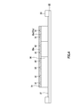
- FIG. 1 is a diagram showing steps of a wafer dicing method according to the present embodiment.
- FIG. 2 is a side view showing a dicing apparatus that can be used in this embodiment.
- FIG. 3 is a side view showing the placing process and the dicing process.
- FIG. 4 is a side view showing the adhesive layer forming step.
- FIG. 5 is a side view showing the expanding step.
- FIG. 6 is a side view showing a semiconductor chip mounting process.
- FIG. 7 is a perspective view showing a dicing apparatus.
- FIG. 8A shows a wafer dicing process, and
- FIG. 8B is a plan view showing an expanding process.
- FIG. 9 is a side view showing a conventional semiconductor chip mounting process, FIG. 9A shows an adhesive film and semiconductor chip placement process, and FIG. 9B shows a bonding process using a heat bonder.
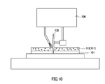
- FIG. 10 is a side view showing a process of cutting the wafer with the adhesive film.
- the wafer dicing method according to the present embodiment includes a placing process, a dicing process, an adhesive layer forming process, and an expanding process.
- the wafer dicing method according to the present embodiment can be performed using, for example, the dicing apparatus 1 shown in FIG.
- the dicing apparatus 1 includes a chuck table 2 on which a jig 22 holding a wafer 20 is placed, an alignment stage 3 that adjusts the position of the chuck table 2, and an imaging unit 4 that visually recognizes a scribe line of the wafer 20.
- a cutting unit 5 for dicing the wafer 20, a nozzle 6 for supplying water to the dicing part, and a control unit 7 for controlling the entire apparatus are provided.
- the chuck table 2 sucks and fixes the jig 22 by a decompression device (not shown), for example.
- the alignment stage 3 moves the chuck table 2 in the x and y directions in FIG. 2 based on instructions from the control unit 7.
- the imaging unit 4 includes, for example, an infrared camera, and includes an optical system that receives light reflected by the surface of the wafer 20, that is, the adhesive surface 20 a of the wafer 20, and an imaging device that captures an image captured by the optical system.
- the imaging unit 4 irradiates light from the bonding surface 20 a or the mounting surface 20 b of the wafer 20 and receives reflected light from the bonding surface 20 a of the wafer 20 or transmitted light that has passed through the wafer 20, thereby allowing the wafer to be captured.
- An image of 20 adhesive surfaces 20a is taken. Then, the imaging unit 4 transmits information on the captured image to the control unit 7.
- the cutting unit 5 cuts the wafer 20 based on an instruction from the control unit 7.
- the cutting unit 5 includes, for example, a blade 8 that cuts the wafer 20.
- the cutting unit 5 presses the rotating blade 8 along the scribe line of the wafer 20 to cut the wafer 20.
- the nozzle 6 supplies water to a dicing portion by the blade 8 based on an instruction from the control unit 7.
- the control unit 7 includes an image processing unit 9 that processes an image captured by the imaging unit 4, a drive unit 10 that receives information on the scribe line of the wafer 20 from the image processing unit 9 and drives the alignment stage 3 and the cutting unit 5. And a nozzle control unit 11 that supplies water from the nozzle 6 to the dicing portion in accordance with the dicing operation of the cutting unit 5.
- the wafer 20 is separated into a plurality of semiconductor chips 30 by the dicing apparatus 1, and examples thereof include a semiconductor wafer such as a silicon wafer.
- the wafer 20 has an adhesive surface 20a that is electrically connected to the substrate electrode 34 formed on the mounting portion of the substrate 33 via the adhesive layer 31 when the one surface is separated into semiconductor chips 30 and the other surface.
- the surface is a mounting surface 20 b that is fixed to the jig 22 by being attached to the dicing tape 21.
- a chip electrode 32 that is conductively connected to an electrode on the substrate 33 side is provided for each semiconductor chip 30 divided by the scribe line 25.
- the jig 22 for fixing the wafer 20 includes, for example, a ring-shaped or frame-shaped frame 23 having a diameter larger than the diameter of the wafer 20 and a dicing tape 21 attached to the frame 23.
- the frame 23 is provided so as to be expandable in the x direction and the y direction in FIG.
- the dicing tape 21 is to which the mounting surface 20b of the wafer 20 is affixed.
- the dicing tape 21 fixes the wafer 20 in the dicing process and prevents chip jumps of the chips divided into the semiconductor chips 30.
- the dicing tape 21 has expandability, and diced wafer 20 is divided into a plurality of semiconductor chips 30.
- the dicing tape 21 is attached to one side of the frame 23, for example, and is spread on the inside of the frame 23.
- the dicing tape 21 is easily separated when the individual semiconductor chips 30 are picked up by being irradiated with ultraviolet rays after the wafer 20 is separated into a plurality of semiconductor chips 30. be able to.
- the wafer 20 is attached to the dicing tape 21 at, for example, the center of one surface of the jig 22.
- Imaging process When the wafer 20 is fixed to the jig 22, the imaging of the bonding surface 20 a of the wafer 20 is performed by the imaging unit 4 in order to determine the scribe line 25 for cutting the wafer 20. Imaging can be performed by irradiating light from the bonding surface 20 a side of the wafer 20 facing the imaging unit 4 and receiving reflected light from the bonding surface 20 a by the imaging unit 4. Alternatively, the imaging may be performed by irradiating light that passes from the chuck table 2 toward the mounting surface 20 b of the wafer 20 to the bonding surface 20 a of the wafer 20 and receiving the transmitted light by the imaging unit 4.
- the imaging unit 4 transmits the captured image information to the control unit 7.
- the controller 7 determines a predetermined scribe line 25 from the image information by the image processor 9. Then, the control unit 7 drives the alignment stage 3 and the cutting unit 5 so that the driving unit 10 cuts the wafer 20 along the scribe line 25 determined by the image processing unit 9.
- the driving unit 10 drives the alignment stage 3 so that one end of the scribe line 25 is positioned below the blade 8. Move 2.
- the driving unit 10 drives the cutting unit 5 to lower the cutting unit 5 while rotating the blade 8, and cuts the wafer 20 with the blade 8.
- the driving unit 10 drives the alignment stage 3 to move the wafer 20 in the x direction.
- the wafer 20 can be divided into a plurality of semiconductor chips 30 by cutting the wafer 20 in a predetermined direction along the scribe line 25. At this time, since the mounting surface 20b is stuck to the dicing tape 21, the wafer 20 is held in a disk shape without chip skipping of each chip divided into the plurality of semiconductor chips 30.
- the nozzle controller 11 supplies water from the nozzle 6 to the dicing portion.
- an adhesive layer 31 is formed on the bonding surface 20 a of the wafer 20.
- the adhesive layer 31 includes an anisotropic conductive adhesive film (ACF) formed by dispersing conductive particles in a binder resin, a conductive adhesive paste, or an insulating adhesive film that does not contain conductive particles. (NCF: Non Particle Conductive Film), an insulating adhesive paste, or a laminate of ACF and NCF.
- ACF anisotropic conductive adhesive film
- NCF Non Particle Conductive Film
- the conductive adhesive paste or the insulating adhesive paste is preheated to about 100 ° C. before being laminated on the adhesive surface 20a of the wafer 20. To B stage.
- the adhesive layer 31 includes, for example, a film forming resin, a liquid curing component, and a curing agent.
- the adhesive layer 31 may contain additives such as various rubber components, softeners, various fillers, and the like.
- Examples of the film forming resin include phenoxy resin, polyester resin, polyamide resin, and polyimide resin.
- the film-forming resin preferably contains a phenoxy resin from the viewpoint of easy availability of materials and connection reliability.
- Examples of the liquid curing component include liquid epoxy resins and acrylates.
- the liquid curing component preferably has two or more functional groups from the viewpoint of connection reliability and stability of the cured product.
- Examples of the curing agent include imidazole, amines, sulfonium salts, onium salts, and phenols when the liquid curing component is a liquid epoxy resin. When the liquid curing component is an acrylate, an organic peroxide can be exemplified as the curing agent.
- Examples of the conductive particles contained in the anisotropic conductive adhesive film and the conductive adhesive paste include any known conductive particles used in anisotropic conductive films, such as nickel, iron, Various metal and metal alloy particles such as copper, aluminum, tin, lead, chromium, cobalt, silver, gold, etc., metal oxide, carbon, graphite, glass, ceramic, plastic, etc. Or what coated the surface of these particle
- examples of the resin particle include an epoxy resin, a phenol resin, an acrylic resin, an acrylonitrile / styrene (AS) resin, a benzoguanamine resin, a divinylbenzene resin, a styrene resin, and the like. Can be mentioned.
- the anisotropic conductive adhesive film and the insulating adhesive film are formed on a release film such as PET that has been subjected to a release treatment from the viewpoint of ease of handling and storage stability.
- a release film such as PET that has been subjected to a release treatment from the viewpoint of ease of handling and storage stability.
- the surface opposite to the surface on which the release film is provided is attached to the adhesive surface 20 a of the wafer 20.
- the anisotropic conductive adhesive film and the insulating adhesive film are formed in the same shape as the wafer 20, for example, in a circular shape.
- an anisotropic conductive adhesive film or an insulating adhesive film is disposed on the adhesive surface 20 a of the wafer 20.
- a heat bonder (not shown) is heated and pressed from above the release film at a predetermined temperature, pressure, and time such that fluidity occurs in the anisotropic conductive adhesive film and the insulating adhesive film, but main curing does not occur.
- the adhesive layer 31 which consists of an anisotropic conductive adhesive film and an insulating adhesive film is formed in the wafer 20 at the adhesive surface 20a.
- the release film is peeled off.
- the heating bonder may be heated and pressed by interposing an elastic body such as silicone rubber between the wafer 20. By interposing the elastic body, the heating bonder can apply pressure evenly over the entire surface of the wafer 20.
- the wafer 20 is expanded to be separated into individual semiconductor chips 30.
- the dicing tape 21 is stretched in the horizontal direction in the x and y directions in FIG.
- the wafer 20 is separated into pieces for each of the plurality of semiconductor chips 30 divided along the scribe line 25.
- the adhesive layer 31 formed on the bonding surface 20a of the wafer 20 is separated from the semiconductor chip 30 along the scribe line 25 by the stress caused by the expansion while the wafer 20 is separated into individual semiconductor chips 30. Cut into the same shape. Therefore, the wafer 20 on which the adhesive layer 31 is formed by the expanding process is divided into pieces for each of the plurality of semiconductor chips 30 provided with the adhesive layer 31 on the mounting surface to the substrate 33.
- the semiconductor chip 30 with the adhesive layer 31 is pulled to peel off the dicing tape 21.
- a plurality of semiconductor chips 30 with the adhesive layers 31 are formed from the wafer 20 on which the adhesive layers 31 are formed.
- the surface that was the adhesive surface 20 a of the wafer 20 becomes an adhesive surface 30 a on which the chip electrode 32 that is conductively connected to the substrate electrode 34 of the substrate 33 is formed.
- An adhesive layer 31 is formed on 30a.
- a bump electrode may be formed as the chip electrode 32.
- the adhesive layer 31 is formed on the adhesive surface 20a after the wafer 20 is diced. Therefore, the wafer 20 can be reliably subjected to predetermined dicing without the adhesive layer 31 impairing the visibility of the scribe line 25.
- the adhesive layer 31 is not affected by chips or dust generated in the dicing process, water supplied from the nozzle 6, etc., is not deteriorated in product life, and can secure conduction reliability. it can.
- the conventional method can be used until the dicing process of the wafer 20, and the manufacturing equipment and the manufacturing process are large. Can be introduced without change.
- the adhesive layer is formed after the dicing process, a conductive adhesive film with low visibility or an insulating adhesive film with a large filler filling amount can be used as the material of the adhesive layer 31. The linear expansion coefficient can be lowered.
- the semiconductor chip 30 with the adhesive layer 31 picked up from the dicing tape 21 is mounted on the substrate 33 constituting the semiconductor integrated circuit via the adhesive layer 31 as shown in FIG.
- the substrate 33 is, for example, a rigid substrate or a flexible substrate, and a substrate electrode 34 that is electrically connected to the chip electrode 32 formed on the bonding surface 30a of the semiconductor chip 30 is formed on the mounting portion where the semiconductor chip 30 is mounted. ing.
- the semiconductor chip 30 can be mounted using, for example, the mounting apparatus 40 shown in FIG.
- the mounting apparatus 40 includes a stage 41 on which the substrate 33 is placed, and a heating bonder 42 that is supported to face the stage 41 and heats and presses the semiconductor chip 30 to the substrate 33.
- the heating bonder 42 is attached with a pressing member 43 made of an elastic body such as an elastomer of silicon rubber, and the semiconductor chip 30 is heated and pressed by the pressing member 43.
- a plurality of semiconductor chips 30 with an adhesive layer 31 are temporarily mounted on the substrate 33 placed on the stage 41.
- the semiconductor chip 30 with the adhesive layer 31 is temporarily mounted with the adhesive surface 30 a provided with the adhesive layer 31 facing the substrate 33.
- the semiconductor chip 30 with the adhesive layer 31 is temporarily mounted by being aligned so that the chip electrode 32 formed on the bonding surface 30a and the substrate electrode 34 provided on the substrate 33 face each other.
- the mounting apparatus 40 lowers the heating bonder 42 and heats and presses the semiconductor chip 30 with the adhesive layer 31 to the substrate 33 with the pressing member 43.
- EBS Elasticity Bonding System
- the binder resin flows in the adhesive layer 31, and the conductive particles are sandwiched between the chip electrode 32 and the substrate electrode 34. At the same time, it hardens in this state. As a result, a mounting body is formed in which the chip electrode 32 of the semiconductor chip 30 is electrically and mechanically connected to the substrate electrode 34 of the substrate 33.
- the adhesive layer 31 is formed on the adhesive surface 20a after the wafer 20 is diced. It is not affected by chips or dust generated in the dicing process, water supplied from the nozzle 6, etc., there is no deterioration in the product life of the mounting body on which the semiconductor chip 30 is mounted, and long-term conduction reliability. Can be secured.
- the case where a plurality of semiconductor chips 30 with the adhesive layer 31 are collectively mounted on the substrate 33 using an elastic body such as an elastomer for the pressing member 43 has been described.
- the method of mounting the semiconductor chip 30 with the adhesive layer 31 on the substrate 33 is not limited to this.
- the semiconductor chip 30 with the adhesive layer 31 may be mounted on the substrate 33 without using an elastic body such as an elastomer.
- the plurality of semiconductor chips 30 with the adhesive layer 31 may be mounted on the substrate 33 one by one.
- the heating bonder 42 may be formed using a hard head such as ceramic or metal, or an ultrasonic head.
- 1 Dicing device 2 chuck table, 3 alignment stage, 4 imaging unit, 5 cutting unit, 6 nozzle, 7 control unit, 8 blade, 9 image processing unit, 10 drive unit, 11 nozzle control unit, 20 wafer, 20a bonding surface 20b mounting surface, 22 jig, 23 frame, 30 semiconductor chip, 30a adhesive surface, 31 adhesive layer, 32 chip electrode, 33 substrate, 34 substrate electrode, 40 mounting device, 41 stage, 42 heating bonder, 43 press Element
Landscapes
- Dicing (AREA)
- Wire Bonding (AREA)
Abstract
ウエハ切断線の視認性を確保し、かつ接着剤層を各チップに簡易に貼着する。ダイシングシート(21)上にウエハ(20)を載置する載置工程と、ウエハ(20)を複数のチップ(30)にダイシングするダイシング工程と、ダイシング工程の後に、ウエハ(20)の表面に接着剤層(31)を形成する接着剤層形成工程と、ウエハ(20)が載置されたダイシングシート(21)を伸張させることによりウエハ(20)及び接着剤層(31)を個片化するエクスパンド工程とを備える。
Description
本発明は、一面に接着剤層が貼着されてなる接着剤層付きチップを形成するウエハのダイシング方法、接着剤層付きチップを実装する実装方法、この接着剤層付きチップの製造方法、及び接着剤層付きチップが実装された実装体に関する。
本出願は、日本国において2011年3月7日に出願された日本特許出願番号特願2011-049336を基礎として優先権を主張するものであり、この出願は参照されることにより、本出願に援用される。
本出願は、日本国において2011年3月7日に出願された日本特許出願番号特願2011-049336を基礎として優先権を主張するものであり、この出願は参照されることにより、本出願に援用される。
従来、半導体集積回路は、半導体集積回路を構成する基板に実装される半導体チップを半導体ウエハから切り出すダイシング工程と、切り出された半導体チップを基板に実装する実装工程とを経て製造されている。
ダイシング工程では、例えば、図7に示すようなダイシング装置100が用いられている。ダイシング装置100は、半導体ウエハ101がセットされる台座102と、半導体ウエハ101を切断するソーブレード103と、台座102上に設けられ半導体ウエハ101を保持する仮固定シート104と、仮固定シート104を伸張させるエクスパンドシート105と、台座102、ソーブレード103及びエクスパンドシート105を制御する制御部106とを備える。エクスパンドシート105は、台座102に真空吸着等によって保持されると共に、上面に仮固定シート104が積層される。
制御部106は、所定のタイミングで台座102を所定角度だけ回転させるとともに、ソーブレード103を駆動させることにより、図8Aに示すように、所定の方向に半導体ウエハ101を切断させる。また、制御部106は、図8Bに示すように、半導体ウエハ101の切断後、エクスパンドシート105を伸張することにより、半導体ウエハ101を複数の半導体チップに個片化する。
個片化された各半導体チップ110は、図9Aに示すように、フィルム状あるいはペースト状の接着剤層111を介して、半導体集積回路の基板112に実装される。接着剤層111は、バインダー樹脂中に導電性粒子を分散させて形成された異方性導電接着フィルムや導電性接着ペースト、あるいは導電性粒子を含まない絶縁性接着フィルムや絶縁性接着ペーストが用いられる。
接着剤層111は、予め基板112の実装部に設けられる。そして、個片化された各半導体チップ110は、接着剤層111上に配置された後、図9Bに示すように、加熱ボンダー113によって所定の温度、圧力、時間だけ加熱押圧される。これにより、接着剤層111のバインダー樹脂が溶融し、対向する半導体チップ110及び基板112の各電極間から流出すると共に導電性粒子が挟持される。この状態でバインダー樹脂が硬化することにより、半導体チップ110は、基板112の実装部との導通が図られるとともに、基板112に接続される。
なお、接着剤層111として、絶縁性接着フィルムや絶縁性接着ペーストを用いた場合には、半導体チップ110に設けられたバンプ電極が基板112の電極と当接することにより導通が図られる。
ところで、上述した半導体集積回路の製造方法においては、複数のサイズで形成される半導体チップ110に応じて、複数のサイズで接着剤層111を形成し基板112上に配置する必要がある。このため同一基板上に複数のサイズの半導体チップ110を実装する場合などでは、一律に機械によって各種サイズの接着剤層111を配置することが困難であり、製造工数やタクトタイムが増加する。
また、各種半導体チップ110のサイズに応じて導電性接着フィルムを形成することや、各種半導体チップ110のサイズに応じて導電性接着フィルムを切断することは、製造コストの増加や、切断による廃棄ロスが生じてしまう。
そこで、図10に示すように、半導体ウエハ101の切断に先立って、予め半導体ウエハ101の表面に接着剤層111となる接着フィルム115を貼着する工法も提案されている。かかる工法によれば、接着フィルム115を複数の半導体素子が形成された半導体ウエハ101表面に接着した後、ダイシングにより接着フィルム115及び半導体チップ110を一括して個片化する。これにより、半導体チップ110の大きさに合わせた接着フィルム115を用意し、それを基板112上に供給する必要がなく、また実装コストの削減が図られる。
しかし、ダイシングにより接着剤層111及び半導体チップ110を一括して個片化する工法では、接着剤層111として異方性導電接着フィルムや異方性導電接着ペーストを用いた場合、バインダー樹脂中に分散されている導電性粒子が接着剤層111の視認性を著しく悪化させてしまい、接着剤層111を通じて半導体ウエハ101の表面に設けられたスクライブラインを視認することが困難となってしまう。
また、異方性導電接着フィルムや絶縁性接着フィルムなどの半導体実装用の樹脂は、線膨張係数を下げるために、フィラーを添加することが必須となっている。しかし、このフィラーが接着剤層111の視認性を更に悪化させている。また、通常、フィラーにはシリカが用いられているが、シリカの添加量を減らしたり、シリカよりも視認性を悪化させないアルミナ等のフィラーを添加したりすることで接着剤層111の視認性を改善することはできるが、線膨張係数を下げる効果が不十分となり、基板112と半導体チップ110との導通信頼性が低くなってしまう。
さらに、ソーブレード103によるダイシングには、切断箇所に水を吹き付けながらダイシングを行うことから、水による接着剤層111の製品寿命や性能の劣化が懸念される。また、ダイシングの際に発生する切り粉や塵埃が接着剤層111に付着することによる接続不良の危険もある。また、かかる水や切り粉等による悪影響を抑えるために、接着剤層111に透明なカバーフィルムを貼り付けることも提案されているが、ダイシング後に個片化された半導体チップ110の接着剤層111よりカバーフィルムを剥離することは困難且つ煩雑となる。
そこで、本発明は、ダイシング工程におけるスクライブラインの視認性を悪化させることなく、また接着剤層111を個々の半導体チップ110に簡易に貼着することができるウエハのダイシング方法、実装方法、接着剤層付きチップの製造方法、実装体を提供することを目的とする。
上述した課題を解決するために、本発明に係るウエハのダイシング方法は、ダイシングシート上にウエハを載置する載置工程と、上記ウエハを複数のチップにダイシングするダイシング工程と、上記ダイシング工程の後に、上記ウエハの表面に接着剤層を形成する接着剤層形成工程と、上記ウエハが載置された上記ダイシングシートを伸張させることにより上記ウエハ及び上記接着剤層を個片化するエクスパンド工程とを備えるものである。
また、本発明に係る実装方法は、ダイシングシート上にウエハを載置する載置工程と、上記ウエハを複数のチップにダイシングするダイシング工程と、上記ダイシング工程の後に、上記ウエハの表面に接着剤層を形成する接着剤層形成工程と、上記ウエハが載置された上記ダイシングシートを伸張させることにより上記ウエハ及び上記接着剤層を個片化するエクスパンド工程と、上記個片化された上記ウエハを、上記接着剤層を介して基板の実装部に実装する実装工程とを備えるものである。
また、本発明に係る接着剤層付きチップの製造方法は、ダイシングシート上にウエハを載置する載置工程と、上記ウエハを複数のチップにダイシングするダイシング工程と、上記ダイシング工程の後に、上記ウエハの表面に接着剤層を形成する接着剤層形成工程と、上記ウエハが載置された上記ダイシングシートを伸張させることにより上記ウエハ及び上記接着剤層を個片化するエクスパンド工程とを備えるものである。
また、本発明に係る実装体は、上記記載の方法により製造されたものである。
本発明によれば、ウエハのダイシング後に接着面に接着剤層が形成される。したがって、ウエハは、接着剤層がスクライブラインの視認性を損なうことがなく、確実に所定のダイシング処理を行うことができる。また、接着剤層は、ダイシング工程において発生する切り粉や塵埃、ノズルより供給される水等の影響を受けることがなく、製品寿命の劣化もなく、また導通信頼性を確保することができる。
以下、本発明が適用されたウエハのダイシング方法、実装方法、接着剤層付きチップの製造方法、実装体について、図面を参照しながら詳細に説明する。
図1に示すように、本実施の形態に係るウエハのダイシング方法は、載置工程と、ダイシング工程と、接着剤層形成工程と、エクスパンド工程とを有する。本実施の形態に係るウエハのダイシング方法は、例えば図2に示すダイシング装置1を用いて行うことができる。
[ダイシング装置1]
ダイシング装置1は、ウエハ20を保持した治具22が載置されるチャックテーブル2と、チャックテーブル2の位置を調整するアライメントステージ3と、ウエハ20のスクライブラインを視認するための撮像部4と、ウエハ20のダイシングを行う切削部5と、ダイシング部分に水を供給するノズル6と、装置全体を制御する制御部7とを備える。
ダイシング装置1は、ウエハ20を保持した治具22が載置されるチャックテーブル2と、チャックテーブル2の位置を調整するアライメントステージ3と、ウエハ20のスクライブラインを視認するための撮像部4と、ウエハ20のダイシングを行う切削部5と、ダイシング部分に水を供給するノズル6と、装置全体を制御する制御部7とを備える。
チャックテーブル2は、例えば、図示しない減圧装置により治具22を吸引、固定する。アライメントステージ3は、制御部7の指示に基づいて、チャックテーブル2を図2中x方向およびy方向に移動させる。
撮像部4は、例えば、赤外線カメラで構成され、ウエハ20の表面、すなわち、ウエハ20の接着面20aで反射した光を受光する光学系と、光学系が捉えた像を撮像する撮像素子とを有する。撮像部4は、例えば、ウエハ20の接着面20aあるいは載置面20b側から光を照射し、ウエハ20の接着面20aからの反射光あるいはウエハ20を透過した透過光を受光することにより、ウエハ20の接着面20aの画像を撮像する。そして、撮像部4は、撮像した画像の情報を制御部7に送信する。
切削部5は、制御部7の指示に基づいて、ウエハ20を切削する。切削部5は、例えば、ウエハ20を切削するブレード8を有する。切削部5は、回転するブレード8をウエハ20のスクライブラインに沿って押圧して、ウエハ20を切削する。ノズル6は、制御部7の指示に基づいて、ブレード8によるダイシング部分に水を供給する。
制御部7は、撮像部4が撮影した画像を処理する画像処理部9と、画像処理部9からウエハ20のスクライブラインに関する情報を受けとりアライメントステージ3及び切削部5を駆動する駆動部10と、切削部5のダイシング動作に応じてノズル6からダイシング部分に水を供給させるノズル制御部11とを有する。
[載置工程]
次いで、図3を参照してダイシング装置1のチャックテーブル2にウエハ20を載置する載置工程について説明する。ウエハ20は、ダイシング装置1によって複数の半導体チップ30に個片化されるものであり、例えばシリコンウエハ等の半導体ウエハが挙げられる。ウエハ20は、一方の表面を半導体チップ30に個片化されたときに接着剤層31を介して基板33の実装部に形成された基板電極34と導通接続される接着面20aとし、他方の面をダイシングテープ21に貼着されることにより治具22に固定される載置面20bとする。ウエハ20の接着面20aは、スクライブライン25によって区分される各半導体チップ30毎に、基板33側の電極と導通接続されるチップ電極32が設けられている。
次いで、図3を参照してダイシング装置1のチャックテーブル2にウエハ20を載置する載置工程について説明する。ウエハ20は、ダイシング装置1によって複数の半導体チップ30に個片化されるものであり、例えばシリコンウエハ等の半導体ウエハが挙げられる。ウエハ20は、一方の表面を半導体チップ30に個片化されたときに接着剤層31を介して基板33の実装部に形成された基板電極34と導通接続される接着面20aとし、他方の面をダイシングテープ21に貼着されることにより治具22に固定される載置面20bとする。ウエハ20の接着面20aは、スクライブライン25によって区分される各半導体チップ30毎に、基板33側の電極と導通接続されるチップ電極32が設けられている。
ウエハ20を固定する治具22は、例えば、ウエハ20の直径よりも大きな直径を有するリング状又は枠状のフレーム23と、フレーム23に貼り付けられたダイシングテープ21とを備えている。フレーム23は、チャックテーブル2の指示によって図2中x方向及びy方向にエクスパンド可能に設けられている。
ダイシングテープ21は、ウエハ20の載置面20bが貼り付けられるものであり、ダイシング工程においてウエハ20を固定すると共に、半導体チップ30に分割された各チップのチップ飛びなどを防止するものである。また、ダイシングテープ21は、エクスパンド性を有し、ダイシングされたウエハ20を複数の半導体チップ30に個片化させるものである。
ダイシングテープ21は、例えば、フレーム23の一方の面の側に貼り付けられ、フレーム23の内側に展張されている。ダイシングテープ21としては、例えば、紫外線を照射することにより剥離力が小さくなる粘着フィルムが用いられる。これにより、ダイシングテープ21は、ウエハ20が複数の半導体チップ30に個片化された後、紫外線が照射されることで、個々の半導体チップ30をピックアップするときに半導体チップ30を容易に分離することができる。
載置工程では、ダイシングテープ21に、ウエハ20が、例えば、治具22の一方の面の中央部に貼り付けられる。
[ダイシング工程]
治具22にウエハ20が固定されると、ウエハ20を切断するスクライブライン25を確定するために、撮像部4によるウエハ20の接着面20aの撮像が行われる。撮像は、撮像部4と対峙するウエハ20の接着面20a側から光を照射して接着面20aからの反射光を撮像部4によって受光することにより行うことができる。また、撮像は、チャックテーブル2からウエハ20の載置面20bに向かってウエハ20の接着面20aまで透過する光を照射し、この透過光を撮像部4によって受光してもよい。
治具22にウエハ20が固定されると、ウエハ20を切断するスクライブライン25を確定するために、撮像部4によるウエハ20の接着面20aの撮像が行われる。撮像は、撮像部4と対峙するウエハ20の接着面20a側から光を照射して接着面20aからの反射光を撮像部4によって受光することにより行うことができる。また、撮像は、チャックテーブル2からウエハ20の載置面20bに向かってウエハ20の接着面20aまで透過する光を照射し、この透過光を撮像部4によって受光してもよい。
撮像部4は、撮像した画像情報を制御部7に送信する。制御部7は、画像処理部9によりこの画像情報から所定のスクライブライン25を決定する。そして、制御部7は、駆動部10が画像処理部9によって決定されたスクライブライン25に沿ってウエハ20を切断するようにアライメントステージ3及び切削部5を駆動する。
例えば、スクライブライン25に沿ってウエハ20を図2中x方向に分割する場合、駆動部10は、アライメントステージ3を駆動してスクライブライン25の一端がブレード8の下方に位置するようにチャックテーブル2を移動させる。次いで、駆動部10は、切削部5を駆動して、ブレード8を回転させた状態で切削部5を降下させ、ブレード8によってウエハ20を切削する。続いて、駆動部10は、アライメントステージ3を駆動して、ウエハ20をx方向に移動させていく。
このように、ダイシング工程では、スクライブライン25に沿ってウエハ20を所定方向に切断することで、複数の半導体チップ30に分割することができる。このとき、ウエハ20は、載置面20bがダイシングテープ21に貼着されているため、複数の半導体チップ30に分割された各チップのチップ飛びもなく、円盤状に保持されている。
なお、ダイシング工程では、ノズル制御部11によって、ノズル6よりダイシング部分に水が供給される。
[接着剤層形成工程]
次いで、図4に示すように、ウエハ20の接着面20aに接着剤層31が形成される。接着剤層31は、バインダー樹脂中に導電性粒子を分散させて形成された異方性導電接着フィルム(ACF:Anisotropic Conductive Film)や導電性接着ペースト、あるいは導電性粒子を含まない絶縁性接着フィルム(NCF:Non Particle Conductive Film)や絶縁性接着ペースト、ACFとNCFとを積層したものなどを用いて形成される。なお、接着剤層として、導電性接着ペーストや絶縁性接着ペーストを用いる場合、ウエハ20の接着面20aに積層する前に、予め導電性接着ペーストや絶縁性接着ペーストを100℃程度に加熱することによりBステージ化しておく。
次いで、図4に示すように、ウエハ20の接着面20aに接着剤層31が形成される。接着剤層31は、バインダー樹脂中に導電性粒子を分散させて形成された異方性導電接着フィルム(ACF:Anisotropic Conductive Film)や導電性接着ペースト、あるいは導電性粒子を含まない絶縁性接着フィルム(NCF:Non Particle Conductive Film)や絶縁性接着ペースト、ACFとNCFとを積層したものなどを用いて形成される。なお、接着剤層として、導電性接着ペーストや絶縁性接着ペーストを用いる場合、ウエハ20の接着面20aに積層する前に、予め導電性接着ペーストや絶縁性接着ペーストを100℃程度に加熱することによりBステージ化しておく。
接着剤層31は、例えば、膜形成樹脂、液状硬化成分及び硬化剤を含んでいる。また、接着剤層31は、例えば、各種ゴム成分、柔軟剤、各種フィラー類等の添加剤を含んでいてもよい。
膜形成樹脂としては、フェノキシ樹脂、ポリエステル樹脂、ポリアミド樹脂、ポリイミド樹脂を例示できる。膜形成樹脂は、材料の入手の容易さ及び接続信頼性の観点から、フェノキシ樹脂を含むことが好ましい。液状硬化成分としては、液状エポキシ樹脂、アクリレートを例示できる。液状硬化成分は、接続信頼性及び硬化物の安定性の観点から、2以上の官能基を有することが好ましい。硬化剤としては、液状硬化成分が液状エポキシ樹脂の場合は、イミダゾール、アミン類、スルホニウム塩、オニウム塩、フェノール類を例示できる。液状硬化成分がアクリレートの場合には、硬化剤として有機過酸化物を例示できる。
異方性導電接着フィルムや導電性接着ペーストに含有される導電性粒子としては、異方性導電フィルムにおいて使用されている公知の何れの導電性粒子を挙げることができ、例えば、ニッケル、鉄、銅、アルミニウム、錫、鉛、クロム、コバルト、銀、金等の各種金属や金属合金の粒子、金属酸化物、カーボン、グラファイト、ガラス、セラミック、プラスチック等の粒子の表面に金属をコートしたもの、或いは、これらの粒子の表面に更に絶縁薄膜をコートしたもの等が挙げられる。樹脂粒子の表面に金属をコートしたものである場合、樹脂粒子としては、例えば、エポキシ樹脂、フェノール樹脂、アクリル樹脂、アクリロニトリル・スチレン(AS)樹脂、ベンゾグアナミン樹脂、ジビニルベンゼン系樹脂、スチレン系樹脂等の粒子を挙げることができる。
なお、異方性導電接着フィルムや絶縁性接着フィルムは、取り扱いの容易さ、保存安定性等の見地から、剥離処理が施されたPET等の剥離フィルム上に塗布形成される。異方性導電接着フィルムや絶縁性接着フィルムは、ウエハ20の接着面20aには剥離フィルムが設けられた面と反対側の面が貼着される。また、異方性導電接着フィルムや絶縁性接着フィルムの形状は、ウエハ20と同一形状の例えば円形状に形成される。
接着剤層の形成工程では、ウエハ20の接着面20aに異方性導電接着フィルムや絶縁性接着フィルムが配置される。次いで、図示しない加熱ボンダーによって、剥離フィルムの上から異方性導電接着フィルムや絶縁性接着フィルムに流動性が生じるが本硬化は生じない程度の所定の温度、圧力、時間で加熱押圧される。これによりウエハ20は、接着面20aに異方性導電接着フィルムや絶縁性接着フィルムからなる接着剤層31が形成される。接着剤層31の形成後、剥離フィルムは剥離される。
なお、加熱ボンダーは、ウエハ20との間にシリコーンゴム等の弾性体を介在して加熱押圧してもよい。弾性体を介在させることにより、加熱ボンダーは、ウエハ20の全面に亘って均等に圧力をかけることができる。
[エクスパンド工程]
次いで、図5に示すように、ウエハ20をエクスパンドすることにより各半導体チップ30毎に個片化する。このエクスパンド工程では、チャックテーブル2の指示によってダイシングテープ21が図2中x方向及びy方向に亘って水平方向に伸張される。これにより、ウエハ20は、スクライブライン25に沿って分割された複数の半導体チップ30毎に個片化される。
次いで、図5に示すように、ウエハ20をエクスパンドすることにより各半導体チップ30毎に個片化する。このエクスパンド工程では、チャックテーブル2の指示によってダイシングテープ21が図2中x方向及びy方向に亘って水平方向に伸張される。これにより、ウエハ20は、スクライブライン25に沿って分割された複数の半導体チップ30毎に個片化される。
このとき、ウエハ20の接着面20aに形成された接着剤層31は、ウエハ20が個々の半導体チップ30に個片化されると同時に、エクスパンドによる応力によりスクライブライン25に沿って半導体チップ30と同形状に切断される。したがって、エクスパンド工程により、接着剤層31が形成されたウエハ20は、基板33への実装面に接着剤層31が設けられた複数の半導体チップ30毎に個片化される。
その後、ダイシングテープ21に紫外線を照射するなどにより粘着力を減じさせた後、各接着剤層31付き半導体チップ30を引っ張ることで、ダイシングテープ21より剥離する。これにより、接着剤層31が形成されたウエハ20より、複数の接着剤層31付き半導体チップ30が形成される。この接着剤層31付き半導体チップ30は、ウエハ20の接着面20aであった面が、基板33の基板電極34と導通接続されるチップ電極32が形成された接着面30aとなり、この載置面30aに接着剤層31が形成されている。
なお、半導体チップ30は、接着剤層31として絶縁性接着フィルムを用いる場合には、チップ電極32として、バンプ電極を形成してもよい。
このように、本実施の形態に係るウエハのダイシング方法及び接着剤層付き半導体チップの製造方法によれば、ウエハ20のダイシング後に接着面20aに接着剤層31が形成される。したがって、ウエハ20は、接着剤層31がスクライブライン25の視認性を損なうことがなく、確実に所定のダイシング処理を行うことができる。また、接着剤層31は、ダイシング工程において発生する切り粉や塵埃、ノズル6より供給される水等の影響を受けることがなく、製品寿命の劣化もなく、また導通信頼性を確保することができる。
また、本実施の形態に係るウエハのダイシング方法及び接着剤層付き半導体チップの製造方法によれば、ウエハ20のダイシング工程までは、従来の工法を用いることができ、製造設備や製造工程の大きな変更を伴うことなく導入できる。また、ダイシング工程の後に接着剤層を形成するため、接着剤層31の材料として、視認性の低い導電性接着フィルムやフィラー充填量の多い絶縁性接着フィルムを用いることができ、接着剤層31の線膨張係数を降下させることができる。
[実装工程]
ダイシングテープ21よりピックアップされた接着剤層31付き半導体チップ30は、図6に示すように、接着剤層31を介して半導体集積回路を構成する基板33に実装される。基板33は、例えばリジット基板やフレキシブル基板であり、半導体チップ30が実装される実装部には、半導体チップ30の接着面30aに形成されたチップ電極32と導通接続される基板電極34が形成されている。
ダイシングテープ21よりピックアップされた接着剤層31付き半導体チップ30は、図6に示すように、接着剤層31を介して半導体集積回路を構成する基板33に実装される。基板33は、例えばリジット基板やフレキシブル基板であり、半導体チップ30が実装される実装部には、半導体チップ30の接着面30aに形成されたチップ電極32と導通接続される基板電極34が形成されている。
半導体チップ30は、例えば図6に示す実装装置40を用いて実装することができる。実装装置40は、基板33が載置されるステージ41と、ステージ41と対向して支持され半導体チップ30を基板33に加熱押圧する加熱ボンダー42とを有する。加熱ボンダー42は、シリコンラバーのエラストマーなどの弾性体からなる押圧部材43が取り付けられ、この押圧部材43によって半導体チップ30を加熱押圧する。
実装工程では、まず、ステージ41に載置された基板33上に複数の接着剤層31付き半導体チップ30が仮搭載される。このとき、接着剤層31付き半導体チップ30は、接着剤層31が設けられた接着面30aが基板33に向けて仮搭載される。また、接着剤層31付き半導体チップ30は、接着面30aに形成されたチップ電極32と、基板33に設けられた基板電極34とが対向するように位置合わせされて仮搭載される。
次いで、実装装置40は、加熱ボンダー42を下降させ、押圧部材43で接着剤層31付き半導体チップ30を基板33へ加熱押圧する。このとき、例えば、EBS(Elasticity Bonding System)工法と呼ばれる基板33全体を弾性体で覆った状態で押圧する方法によれば、同一基板上に複数仮搭載された半導体チップ30を一括して圧着することができる。
加熱ボンダー42によって、所定の温度、圧力、時間で加熱押圧されることにより、接着剤層31は、バインダー樹脂が流動し、導電性粒子がチップ電極32と基板電極34との間に挟持されるとともに、この状態で熱硬化する。これにより、半導体チップ30のチップ電極32が基板33の基板電極34と電気的、機械的に接続された実装体が形成される。
ここで、本実施の形態に係る実装方法、及び実装体によれば、上述したように、ウエハ20のダイシング後に接着面20aに接着剤層31が形成されることから、接着剤層31は、ダイシング工程において発生する切り粉や塵埃、ノズル6より供給される水等の影響を受けることがなく、半導体チップ30が実装された実装体の製品寿命の劣化もなく、また長期に亘る導通信頼性を確保することができる。
[コールドエクスパンド]
また、上述したエクスパンド工程において、10℃以下に冷却した環境下で行うと、異方性導電接着フィルムや絶縁性接着フィルムといった接着剤層31は、低温のため伸縮性が低くなっている(コールドエクスパンド)。したがって、かかる低温環境下でエクスパンド工程を実施することにより、ウエハ20の接着面20aに形成された接着剤層31は、より確実にスクライブライン25に沿って半導体チップ30と同形状に切断される。
また、上述したエクスパンド工程において、10℃以下に冷却した環境下で行うと、異方性導電接着フィルムや絶縁性接着フィルムといった接着剤層31は、低温のため伸縮性が低くなっている(コールドエクスパンド)。したがって、かかる低温環境下でエクスパンド工程を実施することにより、ウエハ20の接着面20aに形成された接着剤層31は、より確実にスクライブライン25に沿って半導体チップ30と同形状に切断される。
[その他]
なお、上記実施形態では、押圧部材43にエラストマーなどの弾性体を用いて、複数の接着剤層31付き半導体チップ30を基板33に一括して実装する場合について説明した。しかし、基板33に接着剤層31付き半導体チップ30を実装する方法は、これに限定されない。例えば、エラストマーなどの弾性体を用いずに、接着剤層31付き半導体チップ30を基板33に実装してもよい。また、複数の接着剤層31付き半導体チップ30を、1つずつ基板33に実装してもよい。
なお、上記実施形態では、押圧部材43にエラストマーなどの弾性体を用いて、複数の接着剤層31付き半導体チップ30を基板33に一括して実装する場合について説明した。しかし、基板33に接着剤層31付き半導体チップ30を実装する方法は、これに限定されない。例えば、エラストマーなどの弾性体を用いずに、接着剤層31付き半導体チップ30を基板33に実装してもよい。また、複数の接着剤層31付き半導体チップ30を、1つずつ基板33に実装してもよい。
また、加熱ボンダー42は、セラミックや金属等の硬質ヘッド、あるいは超音波ヘッドを用いて形成してもよい。
1 ダイシング装置、2 チャックテーブル、3 アライメントステージ、4 撮像部、5 切削部、6 ノズル、7 制御部、8 ブレード、9 画像処理部、10 駆動部、11 ノズル制御部、20 ウエハ、20a 接着面、20b 載置面、22 治具、23 フレーム、30 半導体チップ、30a 接着面、31 接着剤層、32 チップ電極、33 基板、34 基板電極、40 実装装置、41 ステージ、42 加熱ボンダー、43 押圧部材
Claims (7)
- ダイシングシート上にウエハを載置する載置工程と、
上記ウエハを複数のチップにダイシングするダイシング工程と、
上記ダイシング工程の後に、上記ウエハの表面に接着剤層を形成する接着剤層形成工程と、
上記ウエハが載置された上記ダイシングシートを伸張させることにより上記ウエハ及び上記接着剤層を個片化するエクスパンド工程とを備えるウエハのダイシング方法。 - 上記エクスパンド工程は、10℃以下で行われるコールドエクスパンドである請求項1記載のウエハのダイシング方法。
- 上記接着剤層形成工程は、接着フィルムを上記ウエハ表面に貼着することにより行う請求項1又は請求項2に記載のウエハのダイシング方法。
- 上記接着フィルムは、絶縁性接着フィルム又は導電性粒子を含有する異方性導電接着フィルムである請求項3記載のウエハのダイシング方法。
- ダイシングシート上にウエハを載置する載置工程と、
上記ウエハを複数のチップにダイシングするダイシング工程と、
上記ダイシング工程の後に、上記ウエハの表面に接着剤層を形成する接着剤層形成工程と、
上記ウエハが載置された上記ダイシングシートを伸張させることにより上記ウエハ及び上記接着剤層を個片化するエクスパンド工程と、
上記個片化された上記ウエハを、上記接着剤層を介して基板の実装部に実装する実装工程とを備える実装方法。 - ダイシングシート上にウエハを載置する載置工程と、
上記ウエハを複数のチップにダイシングするダイシング工程と、
上記ダイシング工程の後に、上記ウエハの表面に接着剤層を形成する接着剤層形成工程と、
上記ウエハが載置された上記ダイシングシートを伸張させることにより上記ウエハ及び上記接着剤層を個片化するエクスパンド工程とを備える接着剤層付きチップの製造方法。 - 請求項5記載の方法により製造された実装体。
Applications Claiming Priority (2)
| Application Number | Priority Date | Filing Date | Title |
|---|---|---|---|
| JP2011-049336 | 2011-03-07 | ||
| JP2011049336A JP2011119767A (ja) | 2011-03-07 | 2011-03-07 | ウエハのダイシング方法、実装方法、接着剤層付きチップの製造方法、実装体 |
Publications (1)
| Publication Number | Publication Date |
|---|---|
| WO2012121307A1 true WO2012121307A1 (ja) | 2012-09-13 |
Family
ID=44284612
Family Applications (1)
| Application Number | Title | Priority Date | Filing Date |
|---|---|---|---|
| PCT/JP2012/055881 Ceased WO2012121307A1 (ja) | 2011-03-07 | 2012-03-07 | ウエハのダイシング方法、実装方法、接着剤層付きチップの製造方法、実装体 |
Country Status (3)
| Country | Link |
|---|---|
| JP (1) | JP2011119767A (ja) |
| TW (1) | TW201237955A (ja) |
| WO (1) | WO2012121307A1 (ja) |
Families Citing this family (6)
| Publication number | Priority date | Publication date | Assignee | Title |
|---|---|---|---|---|
| JP2011119767A (ja) * | 2011-03-07 | 2011-06-16 | Sony Chemical & Information Device Corp | ウエハのダイシング方法、実装方法、接着剤層付きチップの製造方法、実装体 |
| JP6081868B2 (ja) * | 2013-06-18 | 2017-02-15 | 株式会社ディスコ | 切削装置 |
| KR102528636B1 (ko) * | 2016-06-30 | 2023-05-03 | 린텍 가부시키가이샤 | 반도체 가공용 시트 |
| WO2019208071A1 (ja) * | 2018-04-27 | 2019-10-31 | 日東電工株式会社 | 半導体装置製造方法 |
| JP7143156B2 (ja) | 2018-04-27 | 2022-09-28 | 日東電工株式会社 | 半導体装置製造方法 |
| JP7084228B2 (ja) | 2018-06-26 | 2022-06-14 | 日東電工株式会社 | 半導体装置製造方法 |
Citations (5)
| Publication number | Priority date | Publication date | Assignee | Title |
|---|---|---|---|---|
| JP2005116957A (ja) * | 2003-10-10 | 2005-04-28 | Lintec Corp | 半導体装置の製造方法 |
| JP2005223285A (ja) * | 2004-02-09 | 2005-08-18 | Disco Abrasive Syst Ltd | ウエーハの分割方法 |
| JP2006049591A (ja) * | 2004-08-05 | 2006-02-16 | Disco Abrasive Syst Ltd | ウエーハに貼着された接着フィルムの破断方法および破断装置 |
| JP2008098253A (ja) * | 2006-10-06 | 2008-04-24 | Sekisui Chem Co Ltd | 接着剤層付き半導体チップの製造方法、及び、半導体チップ積層体の製造方法 |
| JP2011119767A (ja) * | 2011-03-07 | 2011-06-16 | Sony Chemical & Information Device Corp | ウエハのダイシング方法、実装方法、接着剤層付きチップの製造方法、実装体 |
Family Cites Families (1)
| Publication number | Priority date | Publication date | Assignee | Title |
|---|---|---|---|---|
| JP2009272503A (ja) * | 2008-05-09 | 2009-11-19 | Disco Abrasive Syst Ltd | フィルム状接着剤の破断装置及び破断方法 |
-
2011
- 2011-03-07 JP JP2011049336A patent/JP2011119767A/ja active Pending
-
2012
- 2012-03-07 TW TW101107621A patent/TW201237955A/zh unknown
- 2012-03-07 WO PCT/JP2012/055881 patent/WO2012121307A1/ja not_active Ceased
Patent Citations (5)
| Publication number | Priority date | Publication date | Assignee | Title |
|---|---|---|---|---|
| JP2005116957A (ja) * | 2003-10-10 | 2005-04-28 | Lintec Corp | 半導体装置の製造方法 |
| JP2005223285A (ja) * | 2004-02-09 | 2005-08-18 | Disco Abrasive Syst Ltd | ウエーハの分割方法 |
| JP2006049591A (ja) * | 2004-08-05 | 2006-02-16 | Disco Abrasive Syst Ltd | ウエーハに貼着された接着フィルムの破断方法および破断装置 |
| JP2008098253A (ja) * | 2006-10-06 | 2008-04-24 | Sekisui Chem Co Ltd | 接着剤層付き半導体チップの製造方法、及び、半導体チップ積層体の製造方法 |
| JP2011119767A (ja) * | 2011-03-07 | 2011-06-16 | Sony Chemical & Information Device Corp | ウエハのダイシング方法、実装方法、接着剤層付きチップの製造方法、実装体 |
Also Published As
| Publication number | Publication date |
|---|---|
| JP2011119767A (ja) | 2011-06-16 |
| TW201237955A (en) | 2012-09-16 |
Similar Documents
| Publication | Publication Date | Title |
|---|---|---|
| CN102034747B (zh) | 保护带剥离方法及其装置 | |
| JP5602439B2 (ja) | 加熱装置および実装体の製造方法 | |
| JP5597422B2 (ja) | 接着フィルム付き電子部品の製造方法および実装体の製造方法 | |
| JP5710098B2 (ja) | 半導体装置の製造方法 | |
| JP2011119767A (ja) | ウエハのダイシング方法、実装方法、接着剤層付きチップの製造方法、実装体 | |
| JP2011253940A (ja) | ウエハのダイシング方法、接続方法及び接続構造体 | |
| WO2015162807A1 (ja) | 半導体装置の製造方法 | |
| US11393700B2 (en) | Bonding apparatus and bonding method | |
| WO2011152491A1 (ja) | ウエハのダイシング方法、接続方法及び接続構造体 | |
| CN108140570A (zh) | 保护带和半导体装置的制造方法 | |
| TW202034412A (zh) | 半導體裝置之製造方法 | |
| JPH1167699A (ja) | 半導体装置の製造方法 | |
| JPWO2005036633A1 (ja) | 電子部材の製造方法、及び、接着材付icチップ | |
| JP5493311B2 (ja) | 半導体ウエハのダイシング方法及びこれを用いた半導体装置の製造方法 | |
| JP5272397B2 (ja) | 接着フィルムの貼付装置及び接着フィルムの貼付方法 | |
| KR101035297B1 (ko) | 반도체 장치의 제조 방법 | |
| CN111063631B (zh) | 晶片的加工方法 | |
| JP2005056968A (ja) | 半導体装置の製造方法 | |
| WO2014167948A1 (ja) | 封止シート貼付け方法および封止シート貼付け装置 | |
| JP2018098228A (ja) | 保護テープ、及びこれを用いた半導体装置の製造方法 | |
| JP5849405B2 (ja) | 半導体装置の製造方法 | |
| JP2011228362A (ja) | 半導体装置の製造方法 | |
| JP6752722B2 (ja) | 実装装置および実装方法 | |
| JP5023664B2 (ja) | 半導体装置の製造方法 | |
| JP6058414B2 (ja) | 半導体チップの製造方法 |
Legal Events
| Date | Code | Title | Description |
|---|---|---|---|
| 121 | Ep: the epo has been informed by wipo that ep was designated in this application |
Ref document number: 12754391 Country of ref document: EP Kind code of ref document: A1 |
|
| DPE1 | Request for preliminary examination filed after expiration of 19th month from priority date (pct application filed from 20040101) | ||
| NENP | Non-entry into the national phase |
Ref country code: DE |
|
| 122 | Ep: pct application non-entry in european phase |
Ref document number: 12754391 Country of ref document: EP Kind code of ref document: A1 |