WO2012121143A1 - 光硬化物の製造方法 - Google Patents
光硬化物の製造方法 Download PDFInfo
- Publication number
- WO2012121143A1 WO2012121143A1 PCT/JP2012/055369 JP2012055369W WO2012121143A1 WO 2012121143 A1 WO2012121143 A1 WO 2012121143A1 JP 2012055369 W JP2012055369 W JP 2012055369W WO 2012121143 A1 WO2012121143 A1 WO 2012121143A1
- Authority
- WO
- WIPO (PCT)
- Prior art keywords
- mold
- photocurable composition
- photocured product
- substrate
- composition layer
- Prior art date
- Legal status (The legal status is an assumption and is not a legal conclusion. Google has not performed a legal analysis and makes no representation as to the accuracy of the status listed.)
- Ceased
Links
Images


Classifications
-
- G—PHYSICS
- G03—PHOTOGRAPHY; CINEMATOGRAPHY; ANALOGOUS TECHNIQUES USING WAVES OTHER THAN OPTICAL WAVES; ELECTROGRAPHY; HOLOGRAPHY
- G03F—PHOTOMECHANICAL PRODUCTION OF TEXTURED OR PATTERNED SURFACES, e.g. FOR PRINTING, FOR PROCESSING OF SEMICONDUCTOR DEVICES; MATERIALS THEREFOR; ORIGINALS THEREFOR; APPARATUS SPECIALLY ADAPTED THEREFOR
- G03F7/00—Photomechanical, e.g. photolithographic, production of textured or patterned surfaces, e.g. printing surfaces; Materials therefor, e.g. comprising photoresists; Apparatus specially adapted therefor
- G03F7/0002—Lithographic processes using patterning methods other than those involving the exposure to radiation, e.g. by stamping
-
- B—PERFORMING OPERATIONS; TRANSPORTING
- B82—NANOTECHNOLOGY
- B82Y—SPECIFIC USES OR APPLICATIONS OF NANOSTRUCTURES; MEASUREMENT OR ANALYSIS OF NANOSTRUCTURES; MANUFACTURE OR TREATMENT OF NANOSTRUCTURES
- B82Y10/00—Nanotechnology for information processing, storage or transmission, e.g. quantum computing or single electron logic
-
- B—PERFORMING OPERATIONS; TRANSPORTING
- B82—NANOTECHNOLOGY
- B82Y—SPECIFIC USES OR APPLICATIONS OF NANOSTRUCTURES; MEASUREMENT OR ANALYSIS OF NANOSTRUCTURES; MANUFACTURE OR TREATMENT OF NANOSTRUCTURES
- B82Y40/00—Manufacture or treatment of nanostructures
Definitions
- the present invention relates to a method for producing a photocured product by photoimprinting.
- Photoimprint is a process in which a photocurable composition layer formed by applying a photocurable composition to a substrate and a mold having a concavo-convex pattern are brought into contact with each other to form the photocurable composition layer on the concavo-convex pattern of the mold. Filling and exposing the photocurable composition layer to a photocured product, and then releasing the mold from the photocured product to obtain a photocured product to which the concavo-convex pattern has been transferred. Since a transferred photocured product can be easily produced, it is a technology that has been attracting attention in recent years (see Patent Document 1).
- the photocured product may be peeled off from the substrate without releasing the mold from the photocured product during the mold release step of releasing the mold from the photocured product.
- the photocured product does not peel from the substrate, a part of the photocured product adheres to the mold, and there is a problem that a photocured product having a desired uneven pattern cannot be obtained. In particular, when the mold is used repeatedly, this problem is remarkable.
- the present invention is a method for producing a photocured product by photoimprinting, and can produce a photocured product that can be favorably repeatedly performed by releasing a mold from the photocured product. It is an object to provide a method.
- the present inventors have found that the adhesion per unit area of the test body obtained by exposing and curing the photocurable composition for imprinting to a member having the same surface as the mold is obtained. And 15 mN / mm 2 or less, it was found that the above problems can be solved, and the present invention has been completed.
- the method for producing a photocured product of the present invention includes a molding step of sandwiching and molding a photocurable composition layer formed of a photocurable composition for imprinting between a substrate and a mold on which an uneven pattern is formed, A photocuring step of exposing the photocurable composition layer to a photocured product, and a mold releasing step of releasing the mold from the photocured product.
- Adhesive force per unit area of a test specimen exposed and cured to a member having the same surface as the mold is 15 mN / mm 2 or less.
- the adhesive force per unit area of a test body that has been cured by exposing the photocurable composition for imprinting to the member having the same surface as the mold is 15 mN / mm 2 or less
- the mold release process for releasing the mold from the photocured product can be performed repeatedly, and the mold is not released from the photocured product and the photocured product is peeled off from the substrate. Although it does not peel, the problem that a part of photocured material adheres to a mold can be prevented. And it can be judged whether a mold release process can be performed favorable only by simple operation of measuring the adhesive force of the test body which exposed and hardened the photocurable composition for imprint to be used.
- FIG. 1 is a cross-sectional view showing an example of a method for producing a photocured product of the present invention
- FIG. 2 is a diagram showing a schematic configuration of an apparatus for measuring adhesive force
- FIG. 3 is an outline of a method for measuring adhesive force
- FIG. 4 is a diagram illustrating an example of a measurement result of adhesion force.
- the method for producing a photocured product of the present invention includes a molding step in which a photocurable composition layer 2 formed of a photocurable composition for imprints is sandwiched between a substrate 1 and a mold 3 on which an uneven pattern is formed.
- the adhesive composition has an adhesion per unit area of 15 mN / mm 2 or less to a member having the same surface as the mold 3 of the test body obtained by exposing and curing the photocurable composition.
- a photocurable composition layer 2 is formed on a substrate 1 by applying a photocurable composition for photoimprinting onto the substrate 1.
- a photocurable composition for photoimprinting onto the substrate 1.
- the photocurable composition is applied on the substrate 1, but the photocurable composition may be applied to the mold 3.
- the substrate 1 may be any substrate as long as the photocurable composition layer 2 can be provided.
- the substrate 1 may be a substrate used in normal optical imprinting.
- Specific examples include transparent inorganic substrates such as glass, silica glass, quartz, and sapphire, transparent synthetic resin substrates such as polycarbonate, polyethylene terephthalate (PET), and triacetyl cellulose, semiconductor substrates such as silicon wafers, GaAs, InAs, Examples thereof include compound semiconductors such as GaN, metals, metal oxides, and the like.
- substrate 1 may be pre-processed for the improvement of the adhesiveness with the photocurable composition layer 2, the application
- Specific examples of the pretreatment include wet surface cleaning, surface modification by plasma and ozone cleaning, treatment with an adhesion improver such as a silane coupling agent, and the like.
- the mold 3 may have a desired uneven pattern on the surface.
- the material of the mold 3 include quartz glass, synthetic quartz glass, silica glass, and ultraviolet rays used for normal light imprints such as synthetic resins such as transparent Teflon (registered trademark) resin, cycloolefin polymer, and silicone rubber. In addition to those exhibiting transparency, it is also possible to exhibit transparency to other active energy rays such as metals and metal oxides such as silicon, silicon carbide, silicon oxide, and nickel.
- the appearance of the mold 3 may be the same as that of the mold 3 used in normal optical imprinting. For example, the appearance may be a rectangular parallelepiped shape or a roll shape.
- the uneven pattern formed on the surface of the mold 3 may be the same as the uneven pattern formed on the surface of the mold used in normal optical imprinting, but is not limited thereto. Not a thing. For example, it is good also as the mold 3 which formed the recessed part by forming the hollow in the surface of the material of a mold, and the part which protruded relatively to the surface side becomes a convex part in this case. Moreover, it is good also as the mold 3 which formed the convex part by providing a permite
- each concave portion of the concave / convex pattern may be a square, a rectangle, a half moon, or a shape similar to these shapes.
- the surface of the mold 3 may be subjected to a mold release treatment.
- a known release treatment agent such as a perfluoro- or hydrocarbon-based polymer compound, an alkoxysilane compound or a trichlorosilane compound, diamond-like carbon, or the like is used by a gas phase method or a liquid phase method. Can be done.
- the photocurable composition for imprints that forms the photocurable composition layer 2 contains a curable monomer that is a compound that has a polymerizable group and reacts and cures upon exposure to ultraviolet rays, active energy rays, and the like. Any of a photo cation curing type that is cured by cationic polymerization by exposure, a radical curing type that is cured by radical polymerization by exposure, and a combination type thereof may be used.
- curable monomer cationic curable monomer
- a compound having a functional group exhibiting photocationic polymerization properties such as an epoxy group, a vinyl group, and an oxetanyl group.
- curable monomer which can be used for the radical curable type photocurable composition for imprints
- (meth) acrylic acid ester, styrene compound, acrylic silane compound, polyfunctional monomer, etc. Is mentioned.
- the photocurable composition for imprints may contain an active energy ray cationic polymerization initiator.
- the active energy ray cationic polymerization initiator can be used without particular limitation as long as it generates an acid upon irradiation with a known active energy ray.
- sulfonium salt, iodonium salt, phosphonium salt, pyridinium salt and the like can be used. Can be mentioned.
- the photocurable composition for imprints may contain an active energy ray radical polymerization initiator.
- the active energy ray radical polymerization initiator include known and commonly used active energy ray radical polymerization initiators such as benzoin / benzoin alkyl ethers, acetophenones, anthraquinones, thioxanthones, ketals, benzophenones, and xanthones. And can be used in combination with known and commonly used sensitizers.
- the photocurable composition for imprints may contain other additives.
- Other additives include solvents, antioxidants, UV absorbers, light stabilizers, silane coupling agents, coating surface improvers, adhesion reducing agents, thermal polymerization inhibitors, leveling agents, surfactants, and storage stability.
- the viscosity of the photocurable composition for imprints is preferably 1 mPa ⁇ s to 10 Pa ⁇ s, more preferably 5 mPa ⁇ s to 5 Pa ⁇ s, and particularly preferably 5 mPa ⁇ s to 3000 mPa ⁇ s. This is because the pattern of the mold 3 can be easily filled with the photocurable composition for imprints.
- the adhesive force per unit area with respect to the member which has the same surface as the mold 3 of the test body which exposed and hardened this photocurable composition for imprints is 15 mN / mm ⁇ 2 > or less. is there.
- the adhesion force per unit area of the test body thus exposed and cured to a member having the same surface as the mold 3 is 15 mN / mm 2 or less.
- the photocured product 4 does not peel from the substrate 1 without being released, and the photocured product 4 does not peel from the substrate 1, but a part of the photocured product adheres to the mold. There is nothing. And if the conventional mold 3 is used repeatedly, that is, if the mold release process is performed a plurality of times, the adhesion between the mold 3 and the photocured product 4 may increase, or a part of the photocured product 4 may adhere to the mold 3. However, according to the method for producing a photocured material of the present invention, for example, even when the mold 3 is used 1000 times or more, a part of the photocured material 4 adheres to the mold 3. Therefore, the problem that a photocured product having a desired uneven pattern cannot be obtained does not occur.
- the adhesive force per unit area is 15 mN / mm 2 or less, the stress applied to the mold 3 in the mold release process is extremely small, and therefore the mold 3 is not broken.
- the magnitude of such an adhesive force is assumed to be determined by the surface state of the mold 3 and the photocurable composition, but the factor is not clear.
- There has never been an imprint method that stipulates the magnitude of such an adhesive force and there is a finding that the release process can be made extremely good by setting the adhesive force per unit area to 15 mN / mm 2 or less. Obtained for the first time by the present inventors. And, it is possible to make the mold release process easy by a simple method of measuring the adhesive force of the test specimen that has been exposed and cured by using the photocurable composition for imprint to be used with the following predetermined apparatus. it can.
- the apparatus for measuring the adhesive force is “a photomechanical resin peeling property mechanical evaluation apparatus” (manufactured by Shimadzu Corporation). As shown in FIG. 2, which is a diagram showing a schematic configuration, this apparatus has a stage 11 on which a substrate 21 is mounted and is rotatable, and is provided directly on the substrate 21 on the rotated stage 11 and has the same surface as the mold 3. A holder 14 having a holder 13 that can hold and lift the member (lens) 12 having light and a light irradiation means for exposing the surface of the substrate 21 through the member 12.
- This light irradiating means is provided at a vertical direction of 45 ° that irradiates the surface of the substrate 21 placed on the stage 11 by reflecting the light emitted from the light source 15 and the light emitted from the light source 15 and transmitting the member 12. It consists of a mirror 16.
- a load cell (not shown) is connected to the member 12 so that the force applied when the member 12 is moved in the vertical direction can be measured.
- the member 12 having the same surface as the mold 3 is a lens having the same shape as that of the mold 3 in the case where a member that is not subjected to the release treatment is used as the mold 3. Is used, the surface of a member having the above shape and made of the same material as that of the mold 3 is subjected to the same release treatment as that of the mold 3.
- FIG. 3 is a diagram showing an outline of a method for measuring the adhesion force
- an imprint photocurable composition is prepared, and a predetermined amount of imprint is applied on the substrate 21 placed on the stage 11.
- the photocurable composition 22 is dropped using, for example, a micropipette (FIGS. 3A and 3B).
- the stage 11 is rotated so that the dripped photocurable composition 22 for imprint is positioned on the lower side in the vertical direction of the member 12 held by the holder 13 (FIG. 3C).
- the holder 13 is lowered so that the distance between the member 12 and the substrate 21 becomes a predetermined value, and the member 12 is brought into contact with the photocurable composition 22 for imprinting (FIG. 3D).
- the holder 13 is further lowered so that the member 12 and the holder 13 do not come into contact with each other (FIG. 3E).
- light is irradiated from the light source 15 to cure the photocurable composition 22 for imprinting, thereby forming a test body 23 (FIG. 3F).
- the holder 13 is raised at a predetermined speed (FIG. 3G), and the specimen 23 is peeled from the member 12 (FIG. 3H).
- the value obtained by dividing the force (adhesion force) F measured by the load cell when the member 12 is peeled from the test body 23 by the contact area between the test body 23 and the member 12 is the adhesion force per unit area.
- An example of the measurement result of the adhesive force is shown in FIG.
- the test body 23 peels from the board
- the test body 23 cannot be peeled from the member 12, and adhesive force cannot be measured. Therefore, the regulation that the adhesive force per unit area is 15 mN / mm 2 or less also stipulates that the test body 23 is not peeled from the substrate 1.
- the method for forming the photocurable composition layer 2 on the substrate 1 or the mold 3 using the photocurable composition for imprints is not particularly limited.
- application or dropping of the photocurable composition specifically, examples of the coating include spin coating, roll coating, dip coating, gravure coating, die coating, curtain coating, inkjet coating, and dispenser coating.
- the photocurable composition layer 2 is sandwiched between the substrate 1 and the mold 3 and molded (molding process).
- the substrate 1 may be pressed against the mold 3, the mold 3 may be pressed against the substrate 1, or both the substrate 1 and the mold 3 may be pressed.
- the force for pressing the substrate 1 and the mold 3 can be set to about 0.01 to 100 MPa, for example.
- the pressing force is preferably as small as possible within the range of pressing.
- pressing by the weight of the mold 3 or the substrate 1 may be performed without applying force. In this way, by pressing the mold 3 against the substrate 1, the uneven pattern of the mold 3 is filled with the photocurable composition layer 2 to be molded.
- the photocurable composition layer 2 and the mold 3 both horizontal and contact the photocurable composition layer 2 and the mold 3, but if the obtained pattern does not interfere with the pattern, keep it horizontal. It is not necessary to limit to.
- a conventional optical imprint apparatus can be used.
- the photocurable composition layer 2 is exposed and cured in a state in which the uneven pattern of the mold 3 is filled with the photocurable composition layer 2 and formed into a photocured product. 4 (photocuring step).
- the light source used for exposure should just be what can irradiate the light of the wavelength which the photocurable composition layer 2 hardens
- Examples of light sources include low pressure mercury lamps, high pressure mercury lamps, ultra high pressure mercury lamps, metal halide lamps, xenon lamps, carbon arcs, mercury xenon lamps, excimer lasers such as XeCl, KrF and ArF, ultraviolet or visible light lasers, and ultraviolet light. Or visible light LED etc. are mentioned.
- the irradiation amount of light may be an amount that can cure the photocurable composition layer 2.
- light is irradiated to the photocurable composition layer 2 from the side of the member which is substantially transparent with respect to the light irradiated among the substrate 1 and the mold 3.
- transferred can be obtained by releasing the mold 3 from the photocured material 4 (mold release process).
- the adhesive force per unit area is 15 mN / mm 2 or less, this mold release step can be performed satisfactorily, and the mold 3 and the photocured product 4 are not cured but photocured.
- the article 4 does not peel off from the substrate 1, and the photocured product 4 does not peel off from the substrate 1, but part of the photocured product does not adhere to the mold.
- the photocured product 4 having a concavo-convex pattern obtained by accurately transferring the concavo-convex pattern of the mold 3 can be formed.
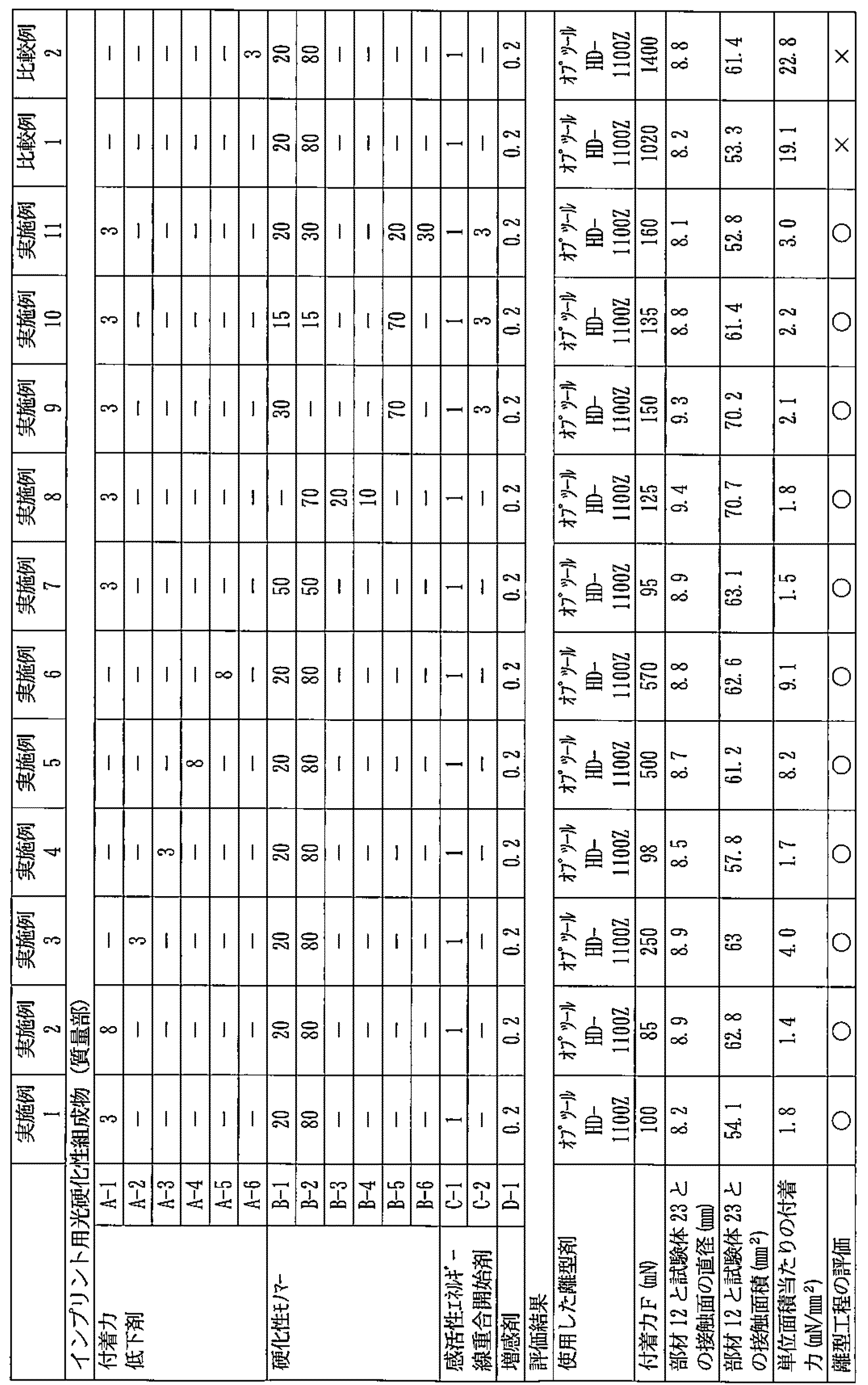
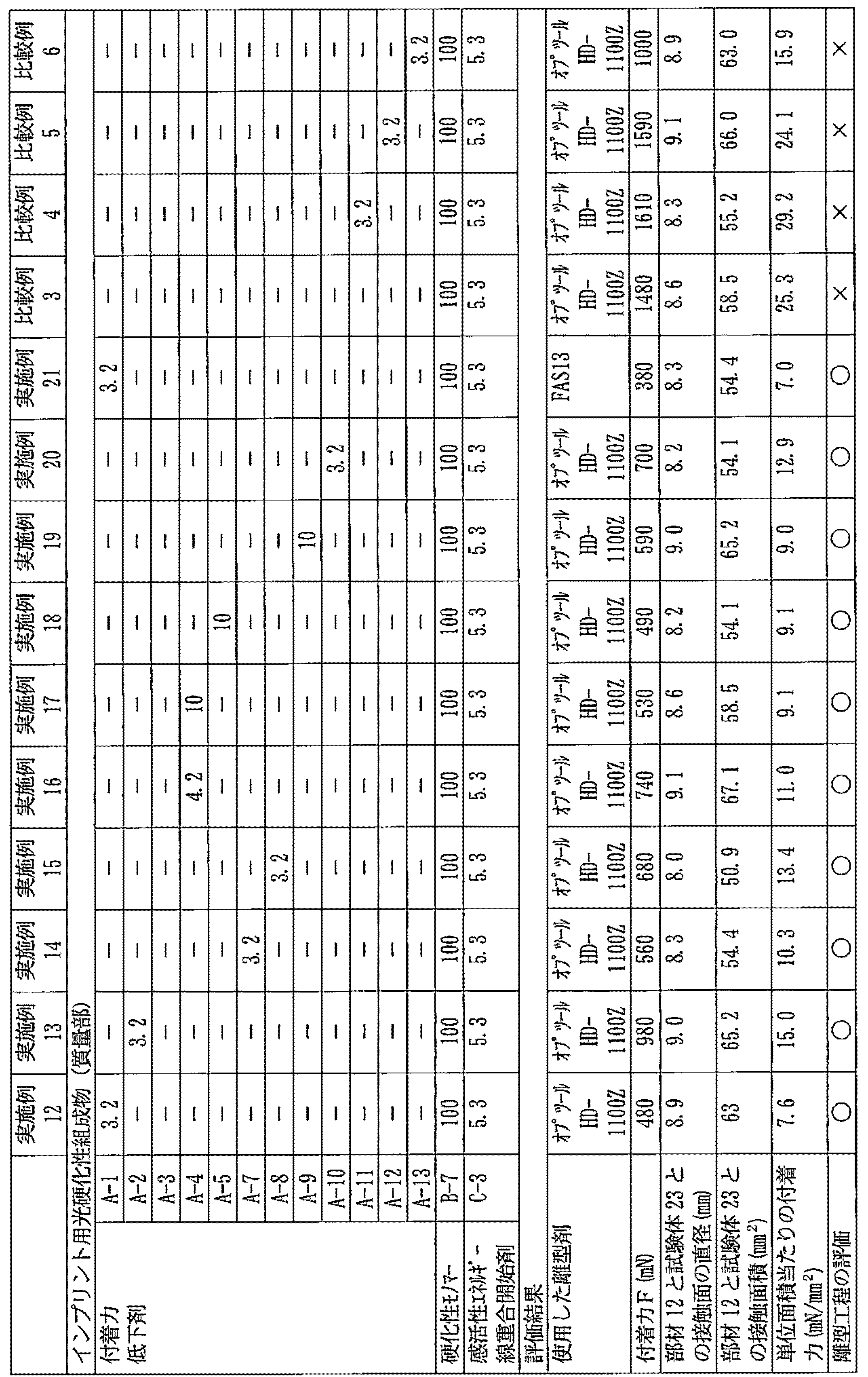
- Examples 1 to 11 and Comparative Examples 1 and 2 are photo-curing type photocurable compositions for imprints. As shown in Table 2, Examples 12 to 21 and Comparative Examples are used. Reference numerals 3 to 6 are radical curable photocurable compositions for imprinting.
- the quartz lens was washed for 15 minutes using an ultraviolet (UV) / ozone cleaner (manufactured by Sen Special Light Source Co., Ltd., PL16-110). Then, it was immersed in a perfluoroether type release agent (Optool HD-1100Z, manufactured by Daikin Industries) for 1 minute. After that, it was pulled up and left at 60 ° C. for 1 hour, washed with a solvent (manufactured by Daikin Industries, OPTOOL HD-ZV), dried by blowing nitrogen gas, and subjected to a release treatment with a release agent. A lens was produced and used as member 12.
- UV ultraviolet
- OPTOOL HD-ZV perfluoroether type release agent
- the photocurable composition for imprinting is exposed and cured using a “photocurable resin peeling property mechanics evaluation apparatus” (manufactured by Shimadzu Corporation) in which the member 12 produced above is placed on the holder 13.
- the adhesion force per unit area of the test body 23 was measured.
- the adhesion force measurement was performed 10 times, and the average value of the adhesion force per unit area obtained from the 6th time to the 10th time was obtained by exposing the photocurable composition for imprinting to be cured per unit area. Adhesive strength was assumed.
- the photocurable composition for imprints is dropped on a 6-inch silicon wafer with a micropipette, the stage 11 is rotated, and the photocurable composition for imprints is the member 12. It was arranged just below. Next, the lowermost surface of the holder 13 was adjusted to a height of 0.500 mm from the surface of the silicon wafer and held for 30 seconds. Then, the adhesive force measurement was started and the holder 13 started to descend.
- ultraviolet light having a wavelength of 350 nm or more emitted from an ultraviolet light source (mercury xenon lamp, manufactured by Mitsunaga Electric Manufacturing Co., Ltd., Supercure 203S) is irradiated with light.
- the test body 23 was produced by irradiating with an amount of 0.65 J / cm 2 (ultraviolet intensity 65 mW / cm 2 at a measurement wavelength of 364 nm, irradiation time 10 seconds) to cure the photocurable composition for imprinting.
- the holder 13 starts to rise at a speed of 0.60 mm / second, the force applied to the load cell is measured at intervals of 10 milliseconds, and the maximum force (adhesion force) when the member 12 peels from the test body 23. F was measured.
- These operations are repeated 10 times, and the diameters of the contact surfaces between the test body 23 and the member 12 are measured in the 6th to 10th measurements, the average value is obtained, and the contact surface between the member 12 and the test body 23 is measured. Diameter (mm).
- the contact area (mm 2 ) between the member 12 and the test body 23 was calculated from the diameter of the contact surface between the member 12 and the test body 23.
- a photocured product 4 was produced by a photoimprinting method using an imprinting apparatus (NM-O801, manufactured by Myeongchang Kiko Co., Ltd.). Specifically, the photocurable composition for imprinting was spin-coated on a 6-inch silicon wafer similar to that used in the measurement of the adhesive force to form the photocurable composition layer 2. . Next, a 10 mm square quartz mold in which line and space, hole, and pillar patterns having a depth range of 350 nm and 350 nm to 10 ⁇ m (micrometer) are formed in the same manner as the quartz lens described above is formed. NTT-AT Co., Ltd.
- NIM-PH350 NIM-PH350
- a mold area of 100 mm 2 is subjected to a force of 100 N (pressing force 1 MPa), and an ultraviolet light source (mercury xenon lamp, UV curing at a wavelength of 350 nm or more emitted from Super Naga 203 (manufactured by Mitsunaga Electric Mfg. Co., Ltd.) with a light irradiation amount of 0.2 J / cm 2 (intensity of 10 mW / cm 2 at a measurement wavelength of 365 nm, irradiation time of 20 seconds) and photocuring.
- the composition layer 2 was cured.
- the photocured material 4 was produced by releasing the mold 3.
- the operation of producing the photocured product 4 by this photoimprinting was performed 1000 times, and the photocured product 4 did not adhere to the mold 3 and the photocured product 4 was not peeled off from the silicon wafer in 1000 times. If the photocured product 4 adheres to the mold 3 once or more, or the photocured product 4 is peeled off from the silicon wafer, it is judged as “x”, and the mold release process is performed. evaluated. The results are shown in Tables 1 and 2.
- the adhesion force per unit area is 15 mN / mm 2 or less, the stress applied to the mold 3 is substantially reduced in the mold release process, and therefore, the mold 3 is less likely to be broken and transferred by normal optical imprinting. Even if it is the mold 3 which has any uneven
Landscapes
- Engineering & Computer Science (AREA)
- Nanotechnology (AREA)
- Chemical & Material Sciences (AREA)
- Physics & Mathematics (AREA)
- Crystallography & Structural Chemistry (AREA)
- General Physics & Mathematics (AREA)
- Condensed Matter Physics & Semiconductors (AREA)
- Manufacturing & Machinery (AREA)
- Mathematical Physics (AREA)
- Theoretical Computer Science (AREA)
- Shaping Of Tube Ends By Bending Or Straightening (AREA)
- Polymerisation Methods In General (AREA)
- Epoxy Resins (AREA)
- Exposure Of Semiconductors, Excluding Electron Or Ion Beam Exposure (AREA)
Abstract
基板と凹凸パターンが形成されたモールドとでインプリント用光硬化性組成物で形成された光硬化性組成物層を挟み込んで成形する成形工程と、前記光硬化性組成物層を露光して光硬化物とする光硬化工程と、該光硬化物から前記モールドを離型する離型工程とを有し、前記インプリント用光硬化性組成物を露光して硬化させた試験体の、前記モールドと同じ表面を有する部材に対する単位面積当たりの付着力が、15mN/mm2以下である。
Description
本発明は、光インプリントによる光硬化物の製造方法に関するものである。
光インプリントは、光硬化性組成物を基板に塗布して形成した光硬化性組成物層と、凹凸パターンが形成されたモールドとを接触させてモールドの凹凸パターンに光硬化性組成物層を充填し、光硬化性組成物層を露光して光硬化物とした後、光硬化物からモールドを離型することにより前記凹凸パターンが転写された光硬化物を得る方法であり、凹凸パターンが転写された光硬化物を簡便に作ることが出来るため、近年注目されている技術である(特許文献1参照)。
しかしながら、光インプリントでは、光硬化物からモールドを離型する離型工程の際に、光硬化物からモールドが離型されずに、光硬化物が基板から剥離してしまう場合があるという問題や、光硬化物は基板から剥離しないが光硬化物の一部がモールドに付着してしまい、所望の凹凸パターンを有する光硬化物を得ることができないという問題がある。特に、モールドを繰り返し使用すると、この問題が顕著である。
本発明はこのような事情に鑑み、光インプリントにより光硬化物を製造する方法であって、光硬化物からモールドを離型する離型工程を繰り返し良好に行なうことができる光硬化物の製造方法を提供することを課題とする。
本発明者らは上記課題を解決するため鋭意検討した結果、インプリント用光硬化性組成物を露光して硬化させた試験体の、モールドと同じ表面を有する部材に対する単位面積当たりの付着力が、15mN/mm2以下である場合に上記課題を解決できることを見出し、本発明を完成するに至った。
すなわち本発明の光硬化物の製造方法は、基板と凹凸パターンが形成されたモールドとでインプリント用光硬化性組成物で形成された光硬化性組成物層を挟み込んで成形する成形工程と、前記光硬化性組成物層を露光して光硬化物とする光硬化工程と、該光硬化物から前記モールドを離型する離型工程とを有し、前記インプリント用光硬化性組成物を露光して硬化させた試験体の、前記モールドと同じ表面を有する部材に対する単位面積当たりの付着力が、15mN/mm2以下であることを特徴とする。
本発明によれば、インプリント用光硬化性組成物を露光して硬化させた試験体の、モールドと同じ表面を有する部材に対する単位面積当たりの付着力が、15mN/mm2以下である場合、モールドを光硬化物から離型する離型工程を繰り返し良好に行なうことができ、光硬化物からモールドが離型されず光硬化物が基板から剥離してしまう問題や、光硬化物が基板から剥離しないが光硬化物の一部がモールドに付着してしまう問題を防ぐことができる。そして、用いるインプリント用光硬化性組成物を露光して硬化させた試験体の付着力を測定するという簡便な操作のみで、離型工程を良好に行えるか否かを判断することができる。
以下、図1~図4を参照して、本発明について詳細に説明する。図1は本発明の光硬化物の製造方法の一例を示す断面図であり、図2は付着力を測定する装置の概略構成を示す図であり、図3は付着力の測定方法の概略を示す図であり、図4は付着力の測定結果の一例を示す図である。
本発明の光硬化物の製造方法は、基板1と凹凸パターンが形成されたモールド3とでインプリント用光硬化性組成物で形成された光硬化性組成物層2を挟み込んで成形する成形工程と、光硬化性組成物層2を露光して光硬化物4とする光硬化工程と、該光硬化物4からモールド3を離型する離型工程とを有し、前記インプリント用光硬化性組成物は、当該光硬化性組成物を露光して硬化させた試験体の、モールド3と同じ表面を有する部材に対する単位面積当たりの付着力が、15mN/mm2以下である。
具体的には、まず、図1(a)に示すように、光インプリント用光硬化性組成物を基板1上に塗布等することにより、基板1上に光硬化性組成物層2を形成させる。なお、図1(a)では基板1上に光硬化性組成物を塗布したが、モールド3に光硬化性組成物を塗布等してもよい。
基板1は、光硬化性組成物層2を設けることができるものであればよく、例えば、通常の光インプリントにおいて用いられている基板でよい。具体例としては、ガラス、シリカガラス、石英、サファイア等の透明無機基板、ポリカーボネート、ポリエチレンテレフタラート(PET)、トリアセチルセルロース等の透明合成樹脂基板や、シリコンウェハー等の半導体基板、GaAs、InAs、GaN等の化合物半導体、金属又は金属酸化物等が挙げられる。そして、基板1の表面は、光硬化性組成物層2との接着性の向上や光硬化性組成物層2の塗布状態改良等のために、前処理が施されていてもよい。前処理の具体例としては、湿式の表面洗浄やプラズマ、オゾン洗浄等による表面改質、シランカップリング剤のような接着性向上剤による処理等が挙げられる。
モールド3は、表面に所望の凹凸のパターンが形成されていればよい。モールド3の材質の例としては、石英ガラス、合成石英ガラス、シリカガラスや、透明テフロン(登録商標)樹脂、シクロオレフィンポリマー、シリコーンゴムなどの合成樹脂等の通常光インプリントに用いられる紫外線に対し透過性を示すものの他、シリコン、シリコンカーバイド、酸化シリコン、ニッケル等の金属や金属酸化物等の他の活性エネルギー線に対して透過性を示すのも挙げられる。モールド3の外観は、通常の光インプリントにおいて用いられているモールド3の外観と同様のものでよく、例えば外観が直方体状又はロール状であってよい。
また、モールド3表面に形成されている凹凸のパターンは、通常の光インプリントにおいて用いられているモールドの表面に形成されている凹凸のパターンと同様のものであってよいが、それに限定されるものでない。例えば、モールドの材料の表面に窪みを形成することにより凹部を形成したモールド3としてもよく、この場合、相対的に表面側に突出した部分が凸部となる。また、モールド3の材料の表面に突起を設けることにより凸部を形成したモールド3としてもよく、この場合、相対的に内側に窪んだ部分が凹部となる。さらに、原版の材料の表面に窪みまたは突起を設けることにより形成した凹凸パターンを有する原版を用い、この原版を鋳型として形成したモールド3としてもよい。凹凸のパターンの各凹部の断面の形状は、正方形、長方形、半月形、またはそれら形状に類似した形状等でもよい。
また、光硬化性組成物層2が硬化した光硬化物4とモールド3との離型性を良好にするために、モールド3の表面に、離型処理が施されていてもよい。離型処理は気相法や液相法等によって、パーフルオロ系又は炭化水素系の高分子化合物、アルコキシシラン化合物又はトリクロロシラン化合物、ダイヤモンドライクカーボン等に例示される公知の離型処理剤を用いて行うことができる。
光硬化性組成物層2を形成するインプリント用光硬化性組成物は、重合性基を有し紫外線や活性エネルギー線等の露光により反応して硬化する化合物である硬化性モノマーを含有するものであり、露光によりカチオン重合して硬化する光カチオン硬化タイプ、露光によりラジカル重合して硬化するラジカル硬化タイプ、及び、これらの併用タイプのいずれでもよい。
光カチオン硬化タイプのインプリント用光硬化性組成物に使用できる硬化性モノマー(カチオン硬化性モノマー)としては、エポキシ基、ビニル基や、オキセタニル基等の光カチオン重合性を示す官能基を有する化合物が挙げられる。
また、ラジカル硬化タイプのインプリント用光硬化性組成物に使用できる硬化性モノマー(ラジカル硬化性モノマー)としては、(メタ)アクリル酸エステル、スチレン系化合物、アクリル系シラン化合物や、多官能モノマー等が挙げられる。
インプリント用光硬化性組成物は、感活性エネルギー線カチオン重合開始剤を含んでもよい。感活性エネルギー線カチオン重合開始剤としては、公知の活性エネルギー線を照射して酸を発生するものであれば特に制限なく利用できるが、例えば、スルホニウム塩、ヨードニウム塩、ホスホニウム塩あるいはピリジニウム塩等を挙げることができる。
また、インプリント用光硬化性組成物は、感活性エネルギー線ラジカル重合開始剤を含んでいてもよい。感活性エネルギー線ラジカル重合開始剤としては、ベンゾイン・ベンゾインアルキルエーテル類、アセトフェノン類、アントラキノン類、チオキサントン類、ケタール類、ベンゾフェノン類、キサントン類等の公知慣用の感活性エネルギー線ラジカル重合開始剤が挙げられ、公知慣用の増感剤と組み合わせて用いることができる。
また、インプリント用光硬化性組成物は、その他の添加剤を含有していてもよい。その他の添加剤としては、溶剤、酸化防止剤、紫外線吸収剤、光安定剤、シランカップリング剤、塗面改良剤、付着力低下剤、熱重合禁止剤、レベリング剤、界面活性剤、保存安定剤、可塑剤、滑剤、フィラー、老化防止剤、濡れ性改良剤等が挙げられる。
また、インプリント用光硬化性組成物の粘度は、好ましくは1mPa・s~10Pa・s、さらに好ましくは5mPa・s~5Pa・s、特に好ましくは5mPa・s~3000mPa・sである。インプリント用光硬化性組成物をモールド3のパターンに充填しやすいためである。
そして、本発明においては、このインプリント用光硬化性組成物を露光して硬化させた試験体の、モールド3と同じ表面を有する部材に対する単位面積当たりの付着力が、15mN/mm2以下である。このように露光して硬化させた試験体の、モールド3と同じ表面を有する部材に対する単位面積当たりの付着力が、15mN/mm2以下であるインプリント用光硬化性組成物を用いて光インプリントで光硬化物を製造することにより、後述する実施例に示すように、光硬化物4からモールド3を離型する離型工程を良好に行なうことができ、モールド3と光硬化物4とが離型されずに光硬化物4が基板1から剥離してしまうということがなく、また、光硬化物4は基板1から剥離しないが光硬化物の一部がモールドに付着してしまうということもない。そして、従来モールド3を繰り返して使用する、すなわち離型工程を複数回行なうと、モールド3と光硬化物4との密着力が上がるためか、光硬化物4の一部がモールド3に付着してしまうという問題があったが、本発明の光硬化物の製造方法によれば、例えば、1000回以上モールド3を使用する場合であっても、光硬化物4の一部がモールド3に付着してしまい所望の凹凸パターンを有する光硬化物を得ることができないという問題等が生じない。また、単位面積当たりの付着力が15mN/mm2以下なので、離型工程でモールド3にかかる応力が極小さいため、モールド3が破壊することもない。このような付着力の大きさはモールド3の表面状態と光硬化性組成物により決定されると推測されるが、その要因は明らかでは無い。このような付着力の大きさを規定したインプリント法は従来には無く、単位面積当たりの付着力を15mN/mm2以下とすることにより離型工程を極めて良好にすることができるという知見が、本発明者らにより初めて得られた。そして、用いるインプリント用光硬化性組成物を露光して硬化させた試験体の付着力を下記の所定の装置で測定するという簡便な方法で、容易に離型工程を行える方法とすることができる。
ここで、インプリント用光硬化性組成物を露光して硬化させた試験体の、モールド3と同じ表面を有する部材に対する単位面積当たりの付着力について、以下に説明する。付着力を測定する装置は、「光硬化性樹脂はく離特性の力学評価装置」(株式会社島津製作所製)である。この装置は、概略構成を示す図である図2に示すように、基板21が載置され回転可能なステージ11と、回転したステージ11上の基板21の直上に設けられ、モールド3と同じ表面を有する部材(レンズ)12を保持し昇降可能なホルダー13を有する保持具14と、部材12を介して基板21表面を露光する光照射手段を有する。この光照射手段は、光源15と、光源15から照射された光を反射して部材12を透過させて、ステージ11上に載置された基板21表面へ照射する鉛直方向45°に設けられたミラー16とからなる。そして、部材12にはロードセル(図示なし)が接続されており、部材12を鉛直方向に動かした際にかかる力を測定できる構造となっている。
そして、この装置で、光硬化物の製造方法で実際に使用するモールド3と同じ表面を有する部材であって、所定形状のレンズ、具体的には、直径30mΦ、中心厚12.3mm、縁厚2.0mm、曲率半径16.10mm、焦点距離35mmのレンズを部材12として用い、基板21上に上記インプリント用光硬化性組成物を滴下して、付着力を求める。なお、モールド3と同じ表面を有する部材12とは、モールド3として離型処理しないものを用いる場合は、上記形状を有しモールド3と同じ材質のレンズであり、モールド3として離型処理したものを用いる場合は、上記形状を有しモールド3と同じ材質の部材の表面をモールド3と同じ離型処理したものである。
付着力の測定方法の概略を示す図である図3に示すように、まず、インプリント光硬化性組成物を作製し、ステージ11上に載置された基板21上に所定量のインプリント用光硬化性組成物22を例えばマイクロピペット等を用いて滴下する(図3(a)及び図3(b))。次に、滴下されたインプリント用光硬化性組成物22が、ホルダー13に保持された部材12の鉛直方向下側に位置するように、ステージ11を回転させる(図3(c))。次いで、ホルダー13を下降させて、部材12と基板21との距離を所定値となるようにし、部材12をインプリント用光硬化性組成物22に接触させる(図3(d))。そして、ホルダー13をさらに下降させて、部材12とホルダー13とが接触しない状態にする(図3(e))。次に、光源15から光を照射して、インプリント用光硬化性組成物22を硬化させて、試験体23を形成する(図3(f))。その後、ホルダー13を所定速度で上昇させ(図3(g))、試験体23を部材12から剥離する(図3(h))。この試験体23から部材12を剥離する時にロードセルで測定される力(付着力)Fを、試験体23と部材12との接触面積で割った値が、単位面積当たりの付着力である。付着力の測定結果の一例を図4に示す。なお、試験体23が基板1から剥離してしまうと、部材12から試験体23を剥離できず付着力が測定できない。したがって、単位面積当たりの付着力が15mN/mm2以下という規定は、試験体23が基板1から剥離しない状態であることも規定していることになる。
インプリント用光硬化性組成物を用いて、基板1又はモールド3に光硬化性組成物層2を形成する方法は特に限定されず、例えば、光硬化性組成物の塗布や滴下、具体的には、スピンコート、ロールコート、ディップコート、グラビアコート、ダイコート、カーテンコート、インクジェット塗布及びディスペンサー塗布等が挙げられる。
次に、図1(b)に示すように、基板1とモールド3とで光硬化性組成物層2を挟みこんで成形する(成形工程)。ここで、基板1をモールド3に押圧しても、モールド3を基板1に押圧してもよく、基板1及びモールド3の両方を押圧してもよい。基板1やモールド3を押圧する力は、例えば、0.01~100MPa程度とすることができる。異物混入によるモールド3の破壊を防ぐために、押圧する力は前記押圧の範囲内においても小さいほど好ましい。また、力をかけず、モールド3や基板1の自重による押圧でもよい。このように、基板1に対してモールド3を押圧することにより、モールド3の凹凸パターンに光硬化性組成物層2が充填されて成形される。光硬化性組成物層2とモールド3とを共に水平に保って光硬化性組成物層2とモールド3とを接触させることが好ましいが、得られるパターンに支障が生じなければ、水平に保つことに限定する必要はない。成形工程では、従来の光インプリントにおける装置を用いることができる。
次いで、図1(c)に示すように、モールド3の凹凸パターンに光硬化性組成物層2を充填して成形した状態で光硬化性組成物層2を露光し、硬化させて光硬化物4とする(光硬化工程)。露光に用いる光源は、光硬化性組成物層2が硬化する波長の光を照射できるものであればよい。光源の例としては、低圧水銀ランプ、高圧水銀ランプ、超高圧水銀ランプ、メタルハライドランプ、キセノンランプ、カーボンアーク、水銀キセノンランプ、XeCl、KrFやArF等のエキシマーレーザー、紫外あるいは可視光レーザー、及び紫外あるいは可視光LED等が挙げられる。光の照射量は、光硬化性組成物層2を硬化させることができる量であればよい。本発明を工業的に実施する際には、通常、10J/cm2以下の範囲内で照射量を選定するとよい。なお、基板1及びモールド3のうち、照射する光に対して実質的に透明である部材の側から光硬化性組成物層2に光を照射する。
その後、図1(d)に示すように、光硬化物4からモールド3を離型することにより、モールド3の凹凸パターンが転写された光硬化物4を得ることができる(離型工程)。本発明においては、上記単位面積当たりの付着力が15mN/mm2以下であるので、この離型工程を良好に行なうことができ、モールド3と光硬化物4とが離型されずに光硬化物4が基板1から剥離してしまうということがなく、また、光硬化物4は基板1から剥離しないが光硬化物の一部がモールドに付着してしまうということもない。また、同じモールド3を用いて光インプリントを複数回行っても、モールド3の凹凸パターンを精密に転写した凹凸のパターンを有する光硬化物4を形成することができる。離型する際には、基板1とモールド3とを共に水平に保って離型することが好ましいが、水平に保つことに限定する必要はない。
以下に、本発明を実施例に基づいて説明するが、本発明はこれらの例によって何ら限定されるものではない。
<実施例1~21及び比較例1~6のインプリント用光硬化性組成物の調製>
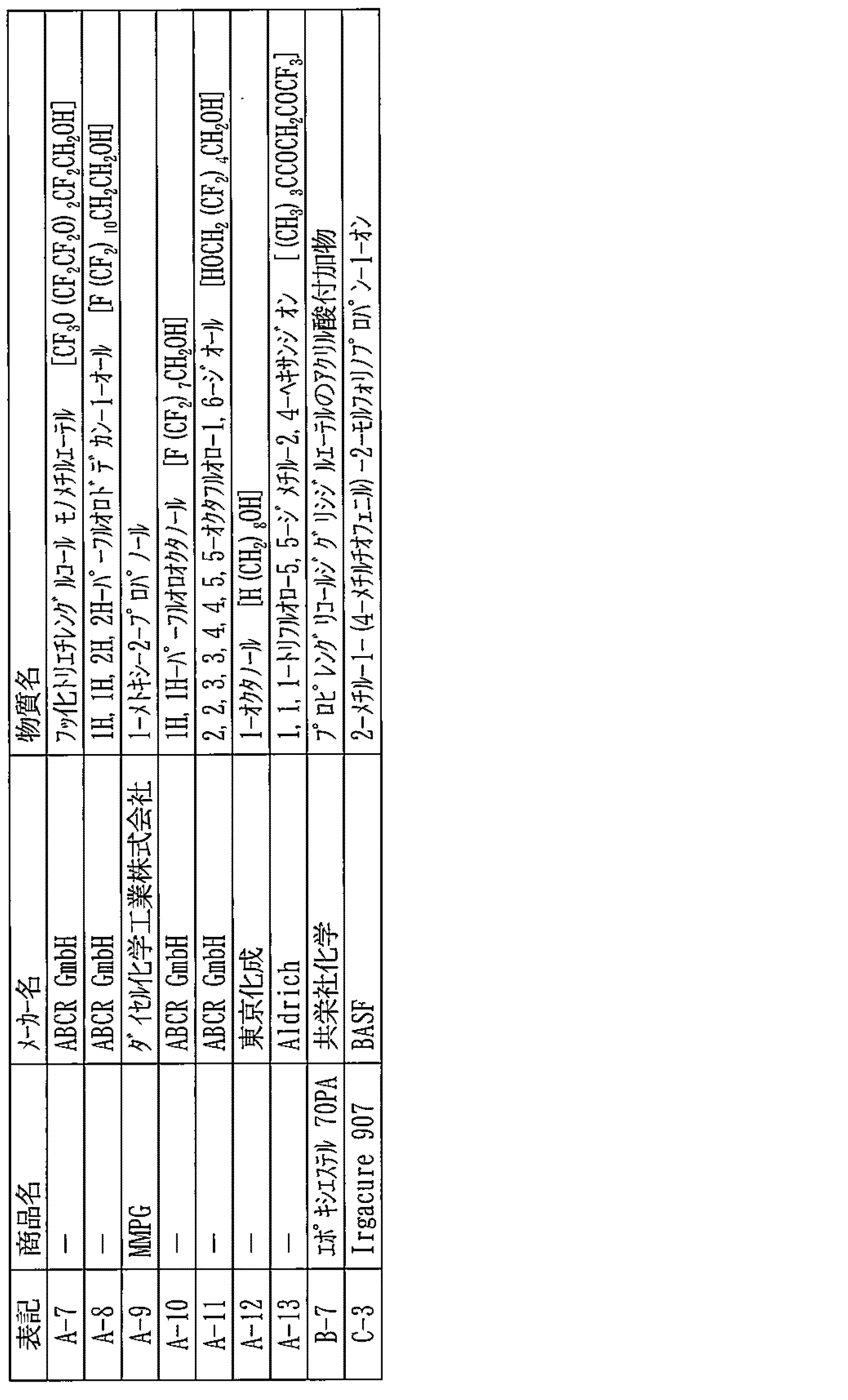
表1及び表2に示す硬化性モノマー100質量部に対して、表1及び表2に示す所定量の感活性エネルギー線重合開始剤及び増感剤を添加して、室温で攪拌して溶解させた後、表1及び表2に示す所定量の付着力低下剤を添加して室温で攪拌し、液状のインプリント用光硬化性組成物実施例1~21及び比較例1~6を調製した。表3及び表4に、硬化性モノマー、付着力低下剤、感活性エネルギー線重合開始剤及び増感剤の具体的な内容を示す。なお、表1に示すように実施例1~11及び比較例1~2は光カチオン硬化タイプのインプリント用光硬化性組成物であり、表2に示すように実施例12~21及び比較例3~6はラジカル硬化タイプのインプリント用光硬化性組成物である。
表1及び表2に示す硬化性モノマー100質量部に対して、表1及び表2に示す所定量の感活性エネルギー線重合開始剤及び増感剤を添加して、室温で攪拌して溶解させた後、表1及び表2に示す所定量の付着力低下剤を添加して室温で攪拌し、液状のインプリント用光硬化性組成物実施例1~21及び比較例1~6を調製した。表3及び表4に、硬化性モノマー、付着力低下剤、感活性エネルギー線重合開始剤及び増感剤の具体的な内容を示す。なお、表1に示すように実施例1~11及び比較例1~2は光カチオン硬化タイプのインプリント用光硬化性組成物であり、表2に示すように実施例12~21及び比較例3~6はラジカル硬化タイプのインプリント用光硬化性組成物である。
<実施例1~21及び比較例1~6のインプリント用光硬化性組成物を露光して硬化した試験体の評価>
<インプリント用光硬化性組成物を露光して硬化した試験体の評価>
(実施例1~20及び比較例1~6用の部材12の作製)
石英レンズ(シグマ光機(株)製、品番SLSQ-30-35、直径30mm、中心厚12.3mm、縁厚2.0mm、曲率半径16.10mm、焦点距離35mm)をクロロホルム中で5分、超音波洗浄器を用いて洗浄した後に、引き上げて乾燥させ、キセノンエキシマ光照射ユニット(シオ電機(株)製、UER-20-172VA)から放射される波長172nmの真空紫外線(VUV線)に圧力1kPaで30分間暴露した。その後、この石英レンズを紫外線(UV)/オゾンクリーナー(セン特殊光源(株)製、PL16-110)を用いて15分間洗浄した。そして、パーフルオロエーテル系の離型剤(ダイキンエ業(株)製、オプツールHD-1100Z)に1分間浸漬した。その後、引き上げて60℃で1時間放置し、溶剤(ダイキンエ業(株)製、オプツールHD-ZV)で洗浄し、窒素ガスを吹き付けて乾燥させ、離型剤で離型処理が施された石英レンズを作製し、部材12とした。
<インプリント用光硬化性組成物を露光して硬化した試験体の評価>
(実施例1~20及び比較例1~6用の部材12の作製)
石英レンズ(シグマ光機(株)製、品番SLSQ-30-35、直径30mm、中心厚12.3mm、縁厚2.0mm、曲率半径16.10mm、焦点距離35mm)をクロロホルム中で5分、超音波洗浄器を用いて洗浄した後に、引き上げて乾燥させ、キセノンエキシマ光照射ユニット(シオ電機(株)製、UER-20-172VA)から放射される波長172nmの真空紫外線(VUV線)に圧力1kPaで30分間暴露した。その後、この石英レンズを紫外線(UV)/オゾンクリーナー(セン特殊光源(株)製、PL16-110)を用いて15分間洗浄した。そして、パーフルオロエーテル系の離型剤(ダイキンエ業(株)製、オプツールHD-1100Z)に1分間浸漬した。その後、引き上げて60℃で1時間放置し、溶剤(ダイキンエ業(株)製、オプツールHD-ZV)で洗浄し、窒素ガスを吹き付けて乾燥させ、離型剤で離型処理が施された石英レンズを作製し、部材12とした。
(実施例21用の部材12の作製)
前述と同じく、クロロホルム洗浄、真空紫外線暴露、紫外線(UV)/オゾンクリーナー洗浄した石英レンズと、10μL(マイクロリットル)の2-(パープルオロヘキシル)エチルトリメトキシシラン(FAS13)(Gelest社製)を入れた3mLのガラス瓶とを、容積120mLのポリエチレンテレフタレート(PTFE)製容器に入れて密栓した。そして、予め150℃に加熱したオーブンに密栓したPTFE製容器を入れた。1時間後にPTFE製容器を取り出して石英モールドを取り出し、FAS13で離型処理を施した石英レンズを作製し、部材12とした。
前述と同じく、クロロホルム洗浄、真空紫外線暴露、紫外線(UV)/オゾンクリーナー洗浄した石英レンズと、10μL(マイクロリットル)の2-(パープルオロヘキシル)エチルトリメトキシシラン(FAS13)(Gelest社製)を入れた3mLのガラス瓶とを、容積120mLのポリエチレンテレフタレート(PTFE)製容器に入れて密栓した。そして、予め150℃に加熱したオーブンに密栓したPTFE製容器を入れた。1時間後にPTFE製容器を取り出して石英モールドを取り出し、FAS13で離型処理を施した石英レンズを作製し、部材12とした。
(付着力の測定)
上記で作製した部材12をホルダー13に載置した「光硬化性樹脂はく離特性の力学評価装置」(株式会社島津製作所製)を用いて、インプリント用光硬化性組成物を露光して硬化させた試験体23の単位面積当りの付着力を測定した。付着力測定を10回行い、6回目から10回目に求めた単位面積当りの付着力の平均値を、インプリント用光硬化性組成物を露光して硬化させた試験体23の単位面積当りの付着力とした。具体的には、各インプリント用光硬化性組成物をマイクロピペットで6インチのシリコンウエハー上に40マイクロリットル滴下し、ステージ11を回転させて、インプリント用光硬化性組成物が部材12の真下に配置されるようにした。次いで、ホルダー13の最下面がシリコンウエハー表面からの高さが0.500mmになるようにし、30秒間保持した後、付着力測定を始め、ホルダー13の下降を始めさせた。ホルダー13の最下面がシリコンウエハー表面からの高さが0.050mmになったところで、紫外線光源(水銀キセノンランプ、三永電機製作所社製、Supercure203S)から放射された波長350nm以上の紫外線を光照射量0.65J/cm2(測定波長364nmでの紫外線強度65mW/cm2、照射時間10秒間)で照射して、インプリント用光硬化性組成物を硬化させて試験体23を作製した。その後、0.60mm/秒の速度でホルダー13の上昇を開始させ、10ミリ秒の間隔でロードセルにかかる力を測定し、試験体23から部材12がはく離するときの最大の力(付着力)Fを測定した。これらの操作を10回繰り返し、6回目から10回目の測定でそれぞれの試験体23と部材12との接触面の直径を測定し、平均値を求め、部材12と試験体23との接触面の直径(mm)とした。部材12と試験体23との接触面の直径から部材12と試験体23との接触面積(mm2)を算出した。6回目から10回目の5回で測定された付着力Fの平均値を求め、部材12と試験体23との接触面積で割り、インプリント用光硬化性組成物を露光して硬化させた試験体23の単位面積当りの付着力とした。結果を表1及び表2に示す。なお、付着力の測定は、大気下で行った。
上記で作製した部材12をホルダー13に載置した「光硬化性樹脂はく離特性の力学評価装置」(株式会社島津製作所製)を用いて、インプリント用光硬化性組成物を露光して硬化させた試験体23の単位面積当りの付着力を測定した。付着力測定を10回行い、6回目から10回目に求めた単位面積当りの付着力の平均値を、インプリント用光硬化性組成物を露光して硬化させた試験体23の単位面積当りの付着力とした。具体的には、各インプリント用光硬化性組成物をマイクロピペットで6インチのシリコンウエハー上に40マイクロリットル滴下し、ステージ11を回転させて、インプリント用光硬化性組成物が部材12の真下に配置されるようにした。次いで、ホルダー13の最下面がシリコンウエハー表面からの高さが0.500mmになるようにし、30秒間保持した後、付着力測定を始め、ホルダー13の下降を始めさせた。ホルダー13の最下面がシリコンウエハー表面からの高さが0.050mmになったところで、紫外線光源(水銀キセノンランプ、三永電機製作所社製、Supercure203S)から放射された波長350nm以上の紫外線を光照射量0.65J/cm2(測定波長364nmでの紫外線強度65mW/cm2、照射時間10秒間)で照射して、インプリント用光硬化性組成物を硬化させて試験体23を作製した。その後、0.60mm/秒の速度でホルダー13の上昇を開始させ、10ミリ秒の間隔でロードセルにかかる力を測定し、試験体23から部材12がはく離するときの最大の力(付着力)Fを測定した。これらの操作を10回繰り返し、6回目から10回目の測定でそれぞれの試験体23と部材12との接触面の直径を測定し、平均値を求め、部材12と試験体23との接触面の直径(mm)とした。部材12と試験体23との接触面の直径から部材12と試験体23との接触面積(mm2)を算出した。6回目から10回目の5回で測定された付着力Fの平均値を求め、部材12と試験体23との接触面積で割り、インプリント用光硬化性組成物を露光して硬化させた試験体23の単位面積当りの付着力とした。結果を表1及び表2に示す。なお、付着力の測定は、大気下で行った。
(インプリントによる光硬化物の作製及び評価)
インプリンティング装置(明昌機工(株)社製、NM-O801)を用いて、光インプリント法により光硬化物4を作製した。具体的には、上記付着力測定の際に用いたものと同様の6インチシリコンウエハー上に、各インプリント用光硬化性組成物をスピン塗布し、光硬化性組成物層2を形成させた。次いで、上記石英レンズと同様に離型処理を施した深さ350nm、350nm~10μm(マイクロメートル)のサイズ範囲のライン&スペース、ホール、ピラーの各パターンが形成されている10mm□の石英モールド(NTT-AT(株)社製、NIM-PH350)を光硬化性組成物層2に接触させて、モールド面積100mm2に100Nの力(押圧する力1MPa)をかけ、紫外線光源(水銀キセノンランプ、三永電機製作所社製、Supercure203s)から放射された波長350nm以上の紫外線を光照射量0.2J/cm2(測定波長365nmにおける強度10mW/cm2、照射時間20秒間)で照射し、光硬化性組成物層2を硬化させた。その後、モールド3を離型することにより、光硬化物4を作製した。この光インプリントにより光硬化物4を作製する操作を1000回行って、1000回ともモールド3に光硬化物4が付着することなく且つ光硬化物4がシリコンウエハーから引き剥がされず良好に離型が行えた場合を「○」、1回以上モールド3に光硬化物4が付着したり、光硬化物4がシリコンウエハーから引き剥がされた場合を「×」と判定して、離型工程を評価した。結果を表1及び表2に示す。
インプリンティング装置(明昌機工(株)社製、NM-O801)を用いて、光インプリント法により光硬化物4を作製した。具体的には、上記付着力測定の際に用いたものと同様の6インチシリコンウエハー上に、各インプリント用光硬化性組成物をスピン塗布し、光硬化性組成物層2を形成させた。次いで、上記石英レンズと同様に離型処理を施した深さ350nm、350nm~10μm(マイクロメートル)のサイズ範囲のライン&スペース、ホール、ピラーの各パターンが形成されている10mm□の石英モールド(NTT-AT(株)社製、NIM-PH350)を光硬化性組成物層2に接触させて、モールド面積100mm2に100Nの力(押圧する力1MPa)をかけ、紫外線光源(水銀キセノンランプ、三永電機製作所社製、Supercure203s)から放射された波長350nm以上の紫外線を光照射量0.2J/cm2(測定波長365nmにおける強度10mW/cm2、照射時間20秒間)で照射し、光硬化性組成物層2を硬化させた。その後、モールド3を離型することにより、光硬化物4を作製した。この光インプリントにより光硬化物4を作製する操作を1000回行って、1000回ともモールド3に光硬化物4が付着することなく且つ光硬化物4がシリコンウエハーから引き剥がされず良好に離型が行えた場合を「○」、1回以上モールド3に光硬化物4が付着したり、光硬化物4がシリコンウエハーから引き剥がされた場合を「×」と判定して、離型工程を評価した。結果を表1及び表2に示す。
この結果、表1および表2に示すように、インプリント用光硬化性組成物を露光して硬化させた試験体23の単位面積当たりの付着力が15mN/mm2以下の実施例1~21を用いた場合は、同一のモールドで1000回光インプリントを行なっても、離型工程を良好に行なうことができた。一方、付着力が15mN/mm2より大きい比較例1~6を用いた場合は、モールド3に光硬化物4の全部または一部が付着し、離型工程を良好に行なえなかった。なお、単位面積当たりの付着力15mN/mm2以下であれば、離型工程において実質的にモールド3にかかる応力が小さくなるため、モールド3の破壊が起こりにくくなり、通常の光インプリントで転写するための如何なる凸凹パターンを有するモールド3であっても、離型工程を繰返し良好に行なうことが出来る。

1、21 基板 2 光硬化性組成物層
3 モールド 4 光硬化物
11 ステージ 12 部材
13 ホルダー 14 保持具
15 光源 16 ミラー
22 インプリント用光硬化性組成物 23 試験体
Claims (1)
- 基板と凹凸パターンが形成されたモールドとでインプリント用光硬化性組成物で形成された光硬化性組成物層を挟み込んで成形する成形工程と、前記光硬化性組成物層を露光して光硬化物とする光硬化工程と、該光硬化物から前記モールドを離型する離型工程とを有し、
前記インプリント用光硬化性組成物を露光して硬化させた試験体の、前記モールドと同じ表面を有する部材に対する単位面積当たりの付着力が、15mN/mm2以下であることを特徴とする光硬化物の製造方法。
Applications Claiming Priority (2)
| Application Number | Priority Date | Filing Date | Title |
|---|---|---|---|
| JP2011-053601 | 2011-03-10 | ||
| JP2011053601A JP2014103135A (ja) | 2011-03-10 | 2011-03-10 | 光硬化物の製造方法 |
Publications (1)
| Publication Number | Publication Date |
|---|---|
| WO2012121143A1 true WO2012121143A1 (ja) | 2012-09-13 |
Family
ID=46798107
Family Applications (1)
| Application Number | Title | Priority Date | Filing Date |
|---|---|---|---|
| PCT/JP2012/055369 Ceased WO2012121143A1 (ja) | 2011-03-10 | 2012-03-02 | 光硬化物の製造方法 |
Country Status (3)
| Country | Link |
|---|---|
| JP (1) | JP2014103135A (ja) |
| TW (1) | TW201245853A (ja) |
| WO (1) | WO2012121143A1 (ja) |
Cited By (1)
| Publication number | Priority date | Publication date | Assignee | Title |
|---|---|---|---|---|
| WO2023086606A1 (en) * | 2021-11-14 | 2023-05-19 | Clark Daniel S | System and method for subzero molding, imprinting, and casting |
Families Citing this family (1)
| Publication number | Priority date | Publication date | Assignee | Title |
|---|---|---|---|---|
| CN105900211A (zh) * | 2014-01-29 | 2016-08-24 | 株式会社大赛璐 | 纳米压印用光固化性组合物、以及使用了该组合物的微细图案的形成方法 |
Citations (6)
| Publication number | Priority date | Publication date | Assignee | Title |
|---|---|---|---|---|
| JP2007523249A (ja) * | 2004-02-23 | 2007-08-16 | モレキュラー・インプリンツ・インコーポレーテッド | インプリントリソグラフィ用の材料 |
| JP2008246729A (ja) * | 2007-03-29 | 2008-10-16 | Sumitomo Heavy Ind Ltd | 成形装置及びそれによる成形方法 |
| JP2008246876A (ja) * | 2007-03-30 | 2008-10-16 | Tokyo Ohka Kogyo Co Ltd | ナノインプリント用の膜形成組成物、並びに構造体の製造方法及び構造体 |
| JP2008296441A (ja) * | 2007-05-31 | 2008-12-11 | Asahi Kasei Electronics Co Ltd | インプリント用感光性樹脂積層体 |
| JP2009191172A (ja) * | 2008-02-14 | 2009-08-27 | Daicel Chem Ind Ltd | ナノインプリント用硬化性樹脂組成物 |
| JP2010076333A (ja) * | 2008-09-26 | 2010-04-08 | Asahi Kasei E-Materials Corp | 成形体、並びに成形体の製造方法、及び成形体を転写した転写体の製造方法 |
-
2011
- 2011-03-10 JP JP2011053601A patent/JP2014103135A/ja not_active Withdrawn
-
2012
- 2012-03-02 WO PCT/JP2012/055369 patent/WO2012121143A1/ja not_active Ceased
- 2012-03-09 TW TW101108042A patent/TW201245853A/zh unknown
Patent Citations (6)
| Publication number | Priority date | Publication date | Assignee | Title |
|---|---|---|---|---|
| JP2007523249A (ja) * | 2004-02-23 | 2007-08-16 | モレキュラー・インプリンツ・インコーポレーテッド | インプリントリソグラフィ用の材料 |
| JP2008246729A (ja) * | 2007-03-29 | 2008-10-16 | Sumitomo Heavy Ind Ltd | 成形装置及びそれによる成形方法 |
| JP2008246876A (ja) * | 2007-03-30 | 2008-10-16 | Tokyo Ohka Kogyo Co Ltd | ナノインプリント用の膜形成組成物、並びに構造体の製造方法及び構造体 |
| JP2008296441A (ja) * | 2007-05-31 | 2008-12-11 | Asahi Kasei Electronics Co Ltd | インプリント用感光性樹脂積層体 |
| JP2009191172A (ja) * | 2008-02-14 | 2009-08-27 | Daicel Chem Ind Ltd | ナノインプリント用硬化性樹脂組成物 |
| JP2010076333A (ja) * | 2008-09-26 | 2010-04-08 | Asahi Kasei E-Materials Corp | 成形体、並びに成形体の製造方法、及び成形体を転写した転写体の製造方法 |
Cited By (1)
| Publication number | Priority date | Publication date | Assignee | Title |
|---|---|---|---|---|
| WO2023086606A1 (en) * | 2021-11-14 | 2023-05-19 | Clark Daniel S | System and method for subzero molding, imprinting, and casting |
Also Published As
| Publication number | Publication date |
|---|---|
| JP2014103135A (ja) | 2014-06-05 |
| TW201245853A (en) | 2012-11-16 |
Similar Documents
| Publication | Publication Date | Title |
|---|---|---|
| TWI585178B (zh) | 壓印用密合膜之製造方法及圖案形成方法 | |
| TWI554826B (zh) | 用於壓印的底層膜形成組成物、疊層物、圖案形成方法及製造半導體裝置之方法 | |
| MX2011005900A (es) | Metodo para producir materiales modelados. | |
| KR20150003187A (ko) | 광 임프린트용 경화성 조성물, 패턴 형성 방법 및 패턴 | |
| KR20150090073A (ko) | 미세 구조체의 제조 방법 및 나노임프린트용 광경화성 조성물 | |
| TW201220974A (en) | Stencils for high-throughput micron-scale etching of substrates and processes of making and using the same | |
| JPWO2013154075A1 (ja) | 微細パターンを表面に有する物品の製造方法 | |
| TWI738776B (zh) | 複製品原盤的製造方法及被成形體的製造方法 | |
| WO2012121143A1 (ja) | 光硬化物の製造方法 | |
| JP5486335B2 (ja) | パターン形成方法 | |
| JP5693925B2 (ja) | 樹脂型、成形体、及び成形体の製造方法 | |
| JP6090732B2 (ja) | 光インプリント方法 | |
| JPWO2013154077A1 (ja) | 微細パターンを表面に有する物品およびその製造方法、ならびに光学物品、その製造方法および複製モールドの製造方法 | |
| JP6491928B2 (ja) | レプリカモールドおよびその製造方法 | |
| CN105619819B (zh) | 一种三维成型装置及方法 | |
| JP6083178B2 (ja) | レジスト基板の製造方法、レプリカテンプレートの製造方法、及びナノインプリントリソグラフィ方法 | |
| TWI774497B (zh) | 複製品原盤 | |
| JP2011071399A (ja) | ナノインプリントパターン形成方法 | |
| JP5744260B2 (ja) | 光硬化性組成物、モールド、樹脂、光学素子の製造方法及び半導体集積回路の製造方法 | |
| JP7147045B2 (ja) | 凹凸構造体の製造方法 | |
| JP2017103369A (ja) | インプリント方法及びインプリントモールド | |
| JP7130113B2 (ja) | 凹凸構造体の製造方法 | |
| JP7094441B2 (ja) | 凹凸構造体の製造方法及び凹凸構造体 | |
| KR20250040551A (ko) | 몰드, 제조 방법, 막 형성 방법, 물품 제조 방법, 및 임프린트 장치 | |
| TW202206253A (zh) | 製造微結構及/或奈米結構之方法及裝置 |
Legal Events
| Date | Code | Title | Description |
|---|---|---|---|
| 121 | Ep: the epo has been informed by wipo that ep was designated in this application |
Ref document number: 12755411 Country of ref document: EP Kind code of ref document: A1 |
|
| NENP | Non-entry into the national phase |
Ref country code: DE |
|
| 122 | Ep: pct application non-entry in european phase |
Ref document number: 12755411 Country of ref document: EP Kind code of ref document: A1 |
|
| NENP | Non-entry into the national phase |
Ref country code: JP |