WO2012120850A1 - プラズマ源及びこのプラズマ源を備えた成膜装置 - Google Patents
プラズマ源及びこのプラズマ源を備えた成膜装置 Download PDFInfo
- Publication number
- WO2012120850A1 WO2012120850A1 PCT/JP2012/001430 JP2012001430W WO2012120850A1 WO 2012120850 A1 WO2012120850 A1 WO 2012120850A1 JP 2012001430 W JP2012001430 W JP 2012001430W WO 2012120850 A1 WO2012120850 A1 WO 2012120850A1
- Authority
- WO
- WIPO (PCT)
- Prior art keywords
- cathode
- plasma
- magnet
- plasma source
- hollow portion
- Prior art date
- Legal status (The legal status is an assumption and is not a legal conclusion. Google has not performed a legal analysis and makes no representation as to the accuracy of the status listed.)
- Ceased
Links
Images







Classifications
-
- H—ELECTRICITY
- H05—ELECTRIC TECHNIQUES NOT OTHERWISE PROVIDED FOR
- H05H—PLASMA TECHNIQUE; PRODUCTION OF ACCELERATED ELECTRICALLY-CHARGED PARTICLES OR OF NEUTRONS; PRODUCTION OR ACCELERATION OF NEUTRAL MOLECULAR OR ATOMIC BEAMS
- H05H1/00—Generating plasma; Handling plasma
- H05H1/24—Generating plasma
- H05H1/46—Generating plasma using applied electromagnetic fields, e.g. high frequency or microwave energy
-
- C—CHEMISTRY; METALLURGY
- C23—COATING METALLIC MATERIAL; COATING MATERIAL WITH METALLIC MATERIAL; CHEMICAL SURFACE TREATMENT; DIFFUSION TREATMENT OF METALLIC MATERIAL; COATING BY VACUUM EVAPORATION, BY SPUTTERING, BY ION IMPLANTATION OR BY CHEMICAL VAPOUR DEPOSITION, IN GENERAL; INHIBITING CORROSION OF METALLIC MATERIAL OR INCRUSTATION IN GENERAL
- C23C—COATING METALLIC MATERIAL; COATING MATERIAL WITH METALLIC MATERIAL; SURFACE TREATMENT OF METALLIC MATERIAL BY DIFFUSION INTO THE SURFACE, BY CHEMICAL CONVERSION OR SUBSTITUTION; COATING BY VACUUM EVAPORATION, BY SPUTTERING, BY ION IMPLANTATION OR BY CHEMICAL VAPOUR DEPOSITION, IN GENERAL
- C23C14/00—Coating by vacuum evaporation, by sputtering or by ion implantation of the coating forming material
- C23C14/22—Coating by vacuum evaporation, by sputtering or by ion implantation of the coating forming material characterised by the process of coating
- C23C14/34—Sputtering
- C23C14/35—Sputtering by application of a magnetic field, e.g. magnetron sputtering
- C23C14/351—Sputtering by application of a magnetic field, e.g. magnetron sputtering using a magnetic field in close vicinity to the substrate
-
- C—CHEMISTRY; METALLURGY
- C23—COATING METALLIC MATERIAL; COATING MATERIAL WITH METALLIC MATERIAL; CHEMICAL SURFACE TREATMENT; DIFFUSION TREATMENT OF METALLIC MATERIAL; COATING BY VACUUM EVAPORATION, BY SPUTTERING, BY ION IMPLANTATION OR BY CHEMICAL VAPOUR DEPOSITION, IN GENERAL; INHIBITING CORROSION OF METALLIC MATERIAL OR INCRUSTATION IN GENERAL
- C23C—COATING METALLIC MATERIAL; COATING MATERIAL WITH METALLIC MATERIAL; SURFACE TREATMENT OF METALLIC MATERIAL BY DIFFUSION INTO THE SURFACE, BY CHEMICAL CONVERSION OR SUBSTITUTION; COATING BY VACUUM EVAPORATION, BY SPUTTERING, BY ION IMPLANTATION OR BY CHEMICAL VAPOUR DEPOSITION, IN GENERAL
- C23C14/00—Coating by vacuum evaporation, by sputtering or by ion implantation of the coating forming material
- C23C14/22—Coating by vacuum evaporation, by sputtering or by ion implantation of the coating forming material characterised by the process of coating
- C23C14/56—Apparatus specially adapted for continuous coating; Arrangements for maintaining the vacuum, e.g. vacuum locks
- C23C14/562—Apparatus specially adapted for continuous coating; Arrangements for maintaining the vacuum, e.g. vacuum locks for coating elongated substrates
-
- H—ELECTRICITY
- H01—ELECTRIC ELEMENTS
- H01J—ELECTRIC DISCHARGE TUBES OR DISCHARGE LAMPS
- H01J37/00—Discharge tubes with provision for introducing objects or material to be exposed to the discharge, e.g. for the purpose of examination or processing thereof
- H01J37/32—Gas-filled discharge tubes
- H01J37/32431—Constructional details of the reactor
- H01J37/32733—Means for moving the material to be treated
- H01J37/32752—Means for moving the material to be treated for moving the material across the discharge
-
- H—ELECTRICITY
- H01—ELECTRIC ELEMENTS
- H01J—ELECTRIC DISCHARGE TUBES OR DISCHARGE LAMPS
- H01J37/00—Discharge tubes with provision for introducing objects or material to be exposed to the discharge, e.g. for the purpose of examination or processing thereof
- H01J37/32—Gas-filled discharge tubes
- H01J37/34—Gas-filled discharge tubes operating with cathodic sputtering
-
- H—ELECTRICITY
- H01—ELECTRIC ELEMENTS
- H01J—ELECTRIC DISCHARGE TUBES OR DISCHARGE LAMPS
- H01J37/00—Discharge tubes with provision for introducing objects or material to be exposed to the discharge, e.g. for the purpose of examination or processing thereof
- H01J37/32—Gas-filled discharge tubes
- H01J37/34—Gas-filled discharge tubes operating with cathodic sputtering
- H01J37/3411—Constructional aspects of the reactor
- H01J37/345—Magnet arrangements in particular for cathodic sputtering apparatus
-
- H—ELECTRICITY
- H01—ELECTRIC ELEMENTS
- H01J—ELECTRIC DISCHARGE TUBES OR DISCHARGE LAMPS
- H01J37/00—Discharge tubes with provision for introducing objects or material to be exposed to the discharge, e.g. for the purpose of examination or processing thereof
- H01J37/32—Gas-filled discharge tubes
- H01J37/34—Gas-filled discharge tubes operating with cathodic sputtering
- H01J37/3411—Constructional aspects of the reactor
- H01J37/345—Magnet arrangements in particular for cathodic sputtering apparatus
- H01J37/3452—Magnet distribution
Definitions
- the present invention relates to a plasma source used when forming a film on an object to be formed in various shapes such as a film, a sheet, a plate or a curved part, and a film forming apparatus for forming a film using the plasma source. Is.
- a raw material gas such as HMDSO (hexamethyldisiloxane) is supplied to the plasma while the film is irradiated with a film formation target such as a film, and the raw material gas is decomposed by the plasma so that a composition such as SiOxCy is formed.
- a film forming process in which an object is deposited on a film forming target is known.
- Patent Document 1 discloses a plasma source used in the film forming process.
- Patent Documents 2 and 3 disclose sputter electrodes that have a structure similar to a plasma source and generate plasma.
- the plasma generation source described in Patent Document 1 includes a cathode having a hollow portion, a magnet that surrounds the entire side surface of the cathode to form a magnetron discharge region in the hollow portion, a side surface of the magnet, and a side surface of the cathode. And a yoke that covers the side surface and the back surface.
- the hollow portion of the cathode is opened on the front surface of the cathode (surface facing the film formation target).
- the sputtering electrode described in Patent Document 2 is a magnetron sputtering electrode for generating plasma in a sputtering apparatus.
- This electrode is disposed on the target (cathode) having a hollow portion formed so that the cross-sectional area increases toward the opening, and on the back surface (the surface opposite to the surface on which the opening is provided) of the target.
- a yoke that covers the side and back surfaces of the magnet and the target.
- the sputtering apparatus disclosed in Patent Document 3 generates plasma in the hollow portion.
- the sputtering apparatus includes a target having a hollow portion and a magnet that surrounds the side surface of the target over the entire circumference.
- the hollow portion opens in front of the cathode.
- the magnet is arranged such that the direction from the S pole to the N pole is directed to the film formation target.
- the yoke confines most of the lines of magnetic force in the plasma source. Therefore, in the plasma generation source, there is a possibility that sufficient magnetic flux density cannot be obtained in the vicinity of the film formation target away from the plasma source, and sufficient film formation may not be performed on the distant film formation target. There is.
- the magnetic field lines emitted from the N pole of the back magnet return to the S pole of the back magnet through the yoke after passing through the hollow portion. At this time, some of the lines of magnetic force emitted from the N pole spread and diverge in the direction of the side surface of the cathode before passing through the hollow portion. For this reason, the magnetic flux density in the film formation target does not increase as in Patent Document 1.
- the plasma generation source and the sputter electrode of Patent Documents 1 to 3 cannot form a magnetic field that provides a sufficiently large magnetic flux density in the vicinity of the film formation target at a distant position.
- the plasma cannot be guided to distant objects.
- the sputter electrodes of Patent Documents 2 and 3 are used in a sputtering apparatus that actively blows a target material by colliding plasma with a target (cathode). For this reason, the sputter electrode has a structure in which the target material that has jumped out from the cathode flows out to the outside (a structure in which the target material can easily jump out).
- An object of the present invention is to provide a plasma source capable of guiding the generated plasma farther from the plasma source and in which the cathode material hardly flows out, and a film forming apparatus using the plasma source.
- a plasma source for irradiating plasma a cathode having a hollow portion surrounding a space in which a magnetron discharge occurs, and a side opposite to the plasma irradiation direction with respect to the cathode.
- a back magnet disposed on the back side, and an outer peripheral magnet that intermittently or continuously surrounds the cathode from a direction orthogonal to the plasma irradiation direction.
- the hollow portion opens at the front surface, which is the surface of the cathode on the plasma irradiation direction side, and all of the magnetic poles of the back magnet and the outer magnet facing the cathode are the same polarity.
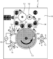
- FIG. 1 is a schematic configuration diagram of a film forming apparatus according to the present embodiment.
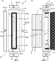
- FIG. 2A is a front view of the plasma source in the film forming apparatus
- FIG. 2B is a side view of the plasma source.
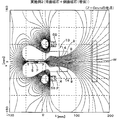
- FIG. 4 is a distribution diagram of magnetic lines of force in the plasma source of Comparative Example 1.
- FIG. 5 is a distribution diagram of magnetic lines of force in the plasma source of Comparative Example 2.
- FIG. 6 is a distribution diagram of magnetic lines of force in the plasma source according to the first embodiment.
- FIG. 7 is a distribution diagram of magnetic lines of force in the plasma source according to the second embodiment.
- FIG. 1 is a schematic configuration diagram of a film forming apparatus according to the present embodiment.
- FIG. 2A is a front view of the plasma source in the film forming apparatus
- FIG. 2B is a side view of the plasma source.
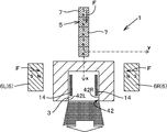
- FIG. 3 is
- FIG. 10 is a schematic configuration diagram of a film forming apparatus including a counter magnet.
- FIG. 11 is a view for explaining the arrangement of the plasma sources in the film forming apparatus according to another embodiment.
- FIG. 12 is a view for explaining the arrangement of the plasma sources in the film forming apparatus according to another embodiment.
- FIG. 13 is a view for explaining the arrangement of plasma sources in a film forming apparatus according to another embodiment.
- FIG. 11 is a view for explaining the arrangement of the plasma sources in the film forming apparatus according to another embodiment.
- FIG. 12 is a view for explaining the arrangement of the plasma sources in the film forming apparatus according to another embodiment.
- FIG. 14 is a schematic configuration diagram for explaining a plasma source having a cathode surrounded by a case.
- FIG. 15 is a schematic configuration diagram for explaining a plasma source in which a cathode, a back magnet, and an outer peripheral magnet are surrounded by a case.
- the film forming apparatus is a so-called roll coater that continuously forms a film on a film or sheet-shaped film forming object W as shown in FIG.
- the film forming apparatus 2 includes a vacuum chamber 10, an uncoiler 11, a coiler 12, a transfer unit, and a plurality (three in this embodiment) of plasma sources 1a to 1c.
- the vacuum chamber 10 is a housing that is hollow inside.
- the vacuum chamber 10 has an airtight structure, and the inside of the vacuum chamber 10 is depressurized by a vacuum evacuation unit (not shown) and is in a vacuum state or a state close to a vacuum.
- the vacuum chamber 10 includes therein an uncoiler 11, a coiler 12, a film forming roller 13, and a plurality of plasma sources 1a to 1c.
- the uncoiler 11 unwinds the coil-shaped film formation target W, and the coiler 12 winds the film formation target W after film formation.
- the conveyance unit includes a plurality of conveyance rollers 20, 20,... And a film formation roller 13, and conveys a sheet-shaped film formation target W, which is a film formation target unwound by the uncoiler 11, to the coiler 12.
- the transport unit transports the film formation target W so that the film formation target W passes through the front side (plasma irradiation direction side) of each plasma source.
- the film forming roller 13 is arranged so that its axial center is directed in the horizontal direction (in the drawing direction in FIG. 1).
- the plurality of transport rollers 20, 20,... are arranged so that the film forming object W in the middle of transport from the uncoiler 11 to the coiler 12 is wound around the film forming roll 13.
- the plurality of plasma sources 1 a to 1 c are arranged on the side of the film forming roll 13 and between the film forming roll 13 and the side wall of the vacuum chamber 10.
- one plasma source 1c is arranged on the right side, and two plasma sources 1a, 1b are arranged on the left side.
- Each of the plasma sources 1a to 1c is arranged so that the opening for plasma irradiation faces the surface of the film forming roll 13. That is, the plasma sources 1a to 1c are arranged so that the opening faces the film formation target W wound around the film formation roll 13.
- the two plasma sources 1a and 1b are arranged side by side along the film formation target W wound around the film formation roll 13, so that the film formation target W is covered over a wide area at a time. Film formation can be performed.
- the plasma source 1c on the right side is connected to one electrode of a plasma power source (not shown), and the other electrode of the plasma power source is connected to the vacuum chamber 10 or the like.
- the left plasma sources 1 a and 1 b are connected to one AC power source (plasma power source) 15.
- the AC power supply 15 is a single-phase AC power supply, and one electrode is connected to one plasma source 1a and the other electrode is connected to the other plasma source 1b.
- each plasma power source When a predetermined voltage is applied from each plasma power source to the plasma sources 1a to 1c, glow discharge is generated in each plasma source 1a to 1c, and the surface of the film formation target W is irradiated with plasma of the ionized source gas. A CVD film is formed.
- the plasma sources 1a to 1c will be described. Since the plasma sources 1a to 1c have the same configuration, only one plasma source (for example, 1a) will be described, and description of the other plasma sources (for example, 1b and 1c) will be omitted. In the following description, the reference numeral of the plasma source is 1.
- the plasma source 1 is provided in the film forming apparatus 2 and generates plasma for forming a CVD film or the like on a belt-like substrate (film forming object W) such as a film or a sheet. As shown in FIGS. 2A to 3, the plasma source 1 includes a cathode 4, a back magnet 5, and an outer peripheral magnet 6.
- the direction indicated by the arrow x in FIG. 2B is the front or front side when the plasma source 1 is described, and the reverse direction of the arrow x is the rear or rear side (back side).
- the direction indicated by the arrow y is the right side when the plasma source 1 is described, and the opposite direction of the arrow y is the left side.
- the direction indicated by the arrow z in FIGS. 2A and 2B is the upper side when the plasma source 1 is described, and the reverse direction of the arrow z is the lower side.
- the cathode 4 is an electrode (cathode) for causing a magnetron discharge necessary for generating plasma in the vicinity of the surface.
- the cathode 4 is a box-like electrode having a length in the vertical direction larger than the width in the left-right direction and having a front surface opened in a rectangular shape toward the front. The dimension in the longitudinal direction of the opening corresponds to the film formation target W.
- this cathode 4 has the hollow part 3 which encloses the space (discharge space) in which a magnetron discharge is generated inside.
- the hollow portion 3 is a long groove-like portion that is recessed from the front surface of the cathode 4 to the rear surface side along the vertical direction, that is, the longitudinal direction of the cathode 4.
- the hollow portion 3 has a bottom wall surface 41 that extends in the vertical direction and faces forward, and a side wall surface (inner side surface) 42 that extends forward from the periphery of the bottom wall surface 41. That is, the discharge space is surrounded by the bottom wall surface 41 and the side wall surface 42.
- the hollow portion 3 surrounds the discharge space so that the front side is open, and is configured to be able to supply a plasma generating gas such as oxygen into the discharge space.
- a plasma generating gas such as oxygen
- the plasma generating gas is ionized by the magnetron discharge generated in the discharge space surrounded by the hollow portion 3, and plasma of the plasma generating gas is generated in the discharge space.
- electrons emitted from the cathode 4 into the hollow portion 3 are generated in the vicinity of the bottom wall surface 41 and the side wall surface 42 (infinite orbit) of the cathode 4 by a magnetic field formed by a back magnet 5 and an outer magnet 6 described later. Continue to circulate in area 14).
- the cathode 4 irradiates the plasma generation gas plasma (oxygen plasma in this embodiment) generated in the hollow portion 3 toward the film formation target side.
- plasma of a source gas such as HMDSO supplied from a supply unit (not shown) is generated.
- the opening on the front surface of the cathode 4 is a slit-shaped opening having a width corresponding to the film formation target W. Thereby, the cathode 4 can irradiate the film formation target W with plasma in a line shape.
- the 42U and the lower surface 42B are formed in a planar shape parallel to each other.
- the left side surface 42L and the right side surface 42R are also formed in a parallel plane.
- the plasma axis (irradiation direction) is parallel to the side wall surface 42 depending on the mounting direction of the back magnet 5 and the outer peripheral magnet 6 and the direction of the magnetic pole, which is a feature of the present invention, that is,
- the four wall surfaces 42U, 42B, 42L, and 42R are set to be parallel to each other.
- the opening shape of the front surface of the cathode 4 that is, the shape of the side wall 42 viewed from the front surface side is rectangular
- the endless orbit region in the above-described magnetron discharge that continues to circulate along the side wall surface 42 of the hollow portion 3 is shown in FIG.
- Plasma generated in the long annular endless track region 14 is drawn outside through the opening on the front surface of the cathode 4 along the magnetic field lines of the magnetic field formed by the back magnet 5 and the outer peripheral magnet 6. Thereby, the extracted plasma becomes a sheet.
- the hollow portion 3 has a shape such that the opening portion of the front surface of the cathode 4 is formed to be narrower than the inner width of the hollow portion 3 to form a narrower (thin) slit shape. Also good. As a result, a plasma source capable of irradiating a thin and uniform sheet-shaped (slit-shaped) plasma while ensuring the size of the discharge space necessary for the magnetron discharge in the hollow portion 3 is realized.
- the back magnet 5 is disposed on the back side (back) of the cathode 4.
- the back magnet 5 of the present embodiment is disposed on the back side of the cathode 4 with a distance from the cathode 4.
- the back magnet 5 is a permanent magnet, for example.
- the back magnet 5 is formed by superimposing a plurality (5 in this embodiment) of rod-like (square bar-shaped in this embodiment) magnets 7 extending in the vertical direction.
- the dimensions of each magnet 7 in the front-rear direction (x direction), left-right direction (y direction), and vertical direction (z direction) are smaller than the hollow part 3 (the inner dimension) of the cathode 4.
- the back magnet 5 of the present embodiment increases the magnetic flux density of the magnetic field formed by superimposing five bar-shaped magnets 7 as compared to the case where only one bar-shaped magnet 7 is provided.
- the outer peripheral magnet 6 is disposed so as to surround the outer periphery of the cathode 4. Specifically, the outer peripheral magnet 6 has a plurality of magnets surrounding the cathode 4 intermittently or continuously from a direction orthogonal to the plasma irradiation direction.
- the outer peripheral magnet 6 of this embodiment has four magnets 6U, 6B, 6L, and 6R.
- the outer periphery magnet 6 may be comprised by one magnet.
- the outer peripheral magnet 6 includes an upper magnet 6U provided at a position away from the upper outer wall surface of the cathode 4 and a lower magnet provided at a position spaced downward from the lower outer wall surface of the cathode 4.
- 6B four magnets, a left magnet 6L provided at a position away from the left outer wall surface of the cathode 4 and a right magnet 6R provided at a position away from the right wall surface of the cathode 4 to the right.
- All of these four magnets 6U, 6B, 6L, and 6R have a rectangular parallelepiped shape or a plate shape.
- the width in the left-right direction (y direction) of the upper magnet 6U is substantially the same as or slightly shorter than that of the cathode 4.
- the depth of the magnet 6U in the front-rear direction (x direction) is substantially the same as or slightly shorter than that of the cathode 4.
- the length of the magnet 6U in the vertical direction (z direction) is substantially the same as or slightly shorter than the width of the back magnet 5 in the horizontal direction (y direction).
- the lower magnet 6B has the same outer shape as the upper magnet 6U.
- the length of the right magnet 6R in the vertical direction (z direction) is substantially the same as or slightly shorter than that of the cathode 4.
- the depth of the magnet 6R in the front-rear direction (x direction) is substantially the same as or slightly shorter than that of the cathode 4.
- the width of the magnet 6 ⁇ / b> R in the left-right direction (y direction) is substantially the same as or slightly shorter than that of the back magnet 5.
- the left magnet 6L has the same outer shape as the right magnet 6R.
- These four magnets 6U, 6B, 6L, and 6R are all arranged at a distance slightly narrower than the thickness of the magnet from the outer peripheral surface of the cathode 4.
- the plasma source 1 of the present embodiment is characterized by the mounting direction of the back magnet 5 and the outer peripheral magnet 6 and the direction of the magnetic pole.
- the shape of the magnet and the magnitude of the magnetic force are appropriately selected.
- the lines of magnetic force passing through the vicinity of the side wall surface 42 of the hollow portion 3 of the cathode 4 are parallel or substantially parallel to any of the four wall surfaces 42U, 42B, 42L, 42R of the hollow portion 3.
- the feature is that the magnetic pole of the portion facing (facing) the cathode 4 of the back magnet 5 and the magnetic pole of the portion facing the cathode 4 of the outer peripheral magnet 6 are equal (having the same polarity). Thereby, the direction of the magnetic pole in each magnet 5 and 6 turns to the cathode 4 side, or turns to the back with respect to the cathode 4 side.
- the direction of the magnetic pole means “the direction from the S pole to the N pole” in the magnet, and is the direction represented by the arrow F in FIGS.
- the direction of the magnetic pole indicates the direction of the lines of magnetic force at the N pole of each magnet.
- the direction F of the magnetic pole is directed toward the cathode 4 or back is that the straight line extending the direction F of the magnetic pole and the outer wall surface of the cathode 4 intersect perpendicularly or substantially perpendicularly.
- the pole (magnetic pole) at the portion facing (opposed) the cathode 4 of the back magnet 5 is an N pole.
- the magnetic poles at the portions facing (opposing) the cathode 4 are N poles.
- the direction F of the magnetic pole of the back magnet 5 is directed toward the cathode 4
- the direction of the magnetic poles of the four magnets 6U, 6B, 6L, 6R constituting the outer peripheral magnet 6 is also directed toward the cathode 4.
- the characteristic of this invention mentioned above is satisfied.
- the south pole of the back magnet 5 faces the cathode 4 and all the south poles of the four magnets 6U, 6B, 6L, 6R constituting the outer peripheral magnet 6 face the cathode 4, each magnet 5 , 6U, 6B, 6L, and 6R, the magnetic pole directions F are opposite to the cathode 4, respectively, and satisfy the above-described features of the present invention.
- FIG. 4 shows a magnetic field line of a plasma source (Comparative Example 1 described later) in which only the back magnet 5 is provided in a state where the aperture member 8 for constricting the opening area is attached to the front surface of the cathode 4 of the present embodiment. It is a distribution map.
- the N pole of the back magnet 5 faces the front
- the S pole faces the back
- the magnetic pole of the back magnet 5 faces the cathode 4.
- the outer peripheral magnet 6 is not provided in the plasma source shown in FIG. 4, the above-described features of the present invention are not satisfied.
- the plasma source of FIG. 1 Comparative Example 1 described later
- FIG. 5 is a magnetic field distribution diagram of a plasma source (Comparative Example 2 to be described later) in which only the outer peripheral magnet 6A is provided in a state where the diaphragm member 8 is attached to the front surface of the cathode 4 of the present embodiment.
- the four magnets constituting the outer peripheral magnet 6 are arranged with the north pole facing backward and the south pole facing forward.
- the magnetic poles of the respective magnets constituting the outer peripheral magnet 6A do not face the cathode 4, and the magnetic poles of the respective magnets face rearward and not toward the cathode 4.
- the magnetic lines of force passing through the discharge space in the cathode 4 do not go forward from the plasma source, pass through the cathode 4 and the throttle member 8 and return to the outer peripheral magnet 6A. For this reason, in the said plasma source, the magnetic force line which goes directly from the inside of the cathode 4 to the film-forming target W does not exist.
- FIG. 6 shows the lines of magnetic force of the plasma source 1A (Example 1 to be described later) in which both the back magnet 5 and the outer peripheral magnet 6 are provided with the aperture member 8 attached to the front surface of the cathode 4 of the present embodiment. It is a distribution map.
- the back magnet 5 is arranged so that the N pole faces the front and the S pole faces the rear.
- the magnets constituting the outer peripheral magnet 6 are arranged so that the N pole faces the cathode 4 and the S pole faces the outside of the cathode 4.
- the discharge space in the cathode 4 has less divergence and the hollow portion.
- the magnetic flux density is increased due to the distribution of magnetic field lines that are nearly parallel to the side wall surface 42 of the third wall.
- the magnetic field lines are distributed with little divergence of magnetic field lines from the plasma source 1A to the film formation target W arranged in front of the plasma source 1A, the film formation target is formed from the plasma source 1A in the vicinity of the film formation target W.
- the density of magnetic flux lines toward the object W (that is, the magnetic flux density) is increased.
- the back magnet 5 and the outer peripheral magnet 6 are arranged with the same magnetic poles facing the cathode 4 side, there is little divergence and the side wall 42 of the cathode 4 in the vicinity of the discharge space in the hollow portion 3 of the cathode 4.
- the magnetic field lines are nearly parallel to the magnetic field, and the magnetic flux density is increased. Further, since the magnetic field lines are distributed with little divergence of magnetic field lines from the plasma source 1A to the film formation target W arranged in front of the plasma source 1A, the film formation target is formed from the plasma source 1A in the vicinity of the film formation target W.
- the density of magnetic flux lines toward the object W (that is, the magnetic flux density) is further increased.
- the magnetron discharge is in an endless orbit region 14 (a region in which electrons emitted from the cathode 4 into the hollow portion 3 circulate at high density by the magnetic field). While the ratio of the vicinity of the bottom wall surface 41 of the hollow part 3 decreases, the ratio of the vicinity of the side wall surface 42 (upper and lower surfaces 42U, 42B, 42L, 42R) of the hollow part 3 increases.
- FIG. 7 shows another plasma source 1B in which both the back magnet 5 and the outer peripheral magnet 6B are provided in a state where the diaphragm member 8 is attached to the front surface of the cathode 4 of the present embodiment (an example described later). It is a magnetic force line distribution figure of 2).
- the plasma source 1 ⁇ / b> B shown in FIG. 7 has stronger magnetic force than the outer peripheral magnet 6 shown in FIG. 6 by using the outer peripheral magnet 6 ⁇ / b> B having a larger thickness than the outer peripheral magnet 6 of the present embodiment.
- the cathode 4 does not have to be configured such that the opening itself on the front surface of the cathode 4 has a narrow slit shape as described above.
- the cathode 4 may include a cathode 4 in which a groove-like hollow portion 3 is formed, and a throttle member 8 that restricts the opening area of the opening of the cathode 4.
- the throttle member 8 has a slit-like opening whose opening width is narrower than that of the front face of the cathode 4 (the opening area is narrowed), and is arranged in front of the hollow portion 3.
- the throttle member 8 may be disposed at a distance from the cathode 4 in front of the hollow portion 3 of the cathode 4.
- the diaphragm member 8 includes an opening 9 that penetrates in a slit shape along the front-rear direction.
- the aperture 9 of the aperture member 8 is formed to have a width narrower than the space between the opposing wall surfaces 42L and 42R in the hollow portion 3 in the cross section along the plasma irradiation direction.
- the opening area is smaller than the opening.
- the aperture member 8 is not electrically connected to the cathode 4 and may be at a potential different from the potential of the cathode 4 (cathode potential).
- Examples 1 and 2 and Comparative Examples 1 and 2 relate to a plasma source including a hollow portion 3 having a height of 350 mm, a width of 25 mm, and a depth of 30 mm. 8 and 9 show the calculation results of how the magnetic flux density changes according to the horizontal distance from the plasma source.
- the back magnet 5 used for each plasma source is a stack of five plate-shaped magnets (height 350 mm ⁇ width 10 mm ⁇ thickness 10 mm) having a residual magnetic flux density of 1.35 [T].
- the back magnet 5 is disposed at a position separated from the rear surface of the cathode 4 by a distance of 5 mm.
- the outer peripheral magnet 6 is composed of four plate-like magnets arranged at a distance of 15 mm from the upper outer surface, lower outer surface, left outer surface, and right outer surface of the cathode 4. Both magnets have a magnetic force with a residual magnetic flux density of 1.195 [T].
- Comparative Example 1 shown in FIG. 4 only the back magnet 5 is provided on the rear surface side of the cathode 4, and the outer peripheral magnet 6 is not provided.
- Comparative Example 2 shown in FIG. 5 only the outer peripheral magnet 6 ⁇ / b> A is provided on the outer peripheral side of the cathode 4, and the rear magnet 5 is not provided.
- the mounting direction of the outer peripheral magnet 6A is arranged such that the direction of the magnetic pole faces in the front-rear direction, and the magnetic pole direction F does not face the cathode 4 as in Examples 1 and 2.
- Example 1 has a magnet arrangement as shown in FIG. Specifically, the back magnet 5 and the outer peripheral magnet 6 are respectively arranged so that the N pole faces the cathode 4. In the second embodiment of FIG. 7, the thickness of the outer peripheral magnet 6B is three times that of the outer peripheral magnet 6 of the first embodiment.
- the origin of this coordinate system is the back magnet 5.
- the center position of the plate-shaped magnet arranged closest to the cathode 4 is determined as a reference.
- the magnetic force line which passes in the hollow part 3 of the cathode 4 does not go ahead from the plasma source 1, but penetrates the cathode 4 and the aperture member 8 to the outer peripheral magnet 6A. I'm back. For this reason, there are no lines of magnetic force directly from the inside of the hollow portion 3 of the cathode 4 to the film formation target W.
- Example 1 shown in FIG. 6 since the outer peripheral magnet 6 is added to Comparative Example 1, the magnetic field lines near the side wall surface 42 in the hollow portion 3 become nearly parallel to the side wall surface 42. The magnetic flux density increases rapidly, thereby causing a stronger magnetron discharge in the hollow portion 3, and the electron confinement efficiency increases rapidly. Further, by adding the outer peripheral magnet 6, the divergence of the magnetic field lines extending forward from the hollow portion 3 is reduced as compared with Comparative Example 1 and Comparative Example 2, and the magnetic field lines directed from the plasma source toward the film formation target W are reduced. The density (magnetic flux density) also increases. As a result, a large amount of plasma generated in the hollow portion 3 is guided to a distance away from the plasma source 1 along the magnetic field lines.
- a stronger permanent magnet (outer peripheral magnet 6B) is used as compared with the outer peripheral magnet 6 of the first embodiment shown in FIG.
- the endless track region 14 is wider than that in the first embodiment, that is, in almost the entire side wall surface 42 in the front-rear direction. Formed along. In other words, the width of the endless track region 14 in the front-rear direction is further increased. Moreover, the magnetic flux density near the side wall surface 42 in the hollow portion 3 further increases. As a result, since the electron confinement efficiency is further improved, it can operate (form plasma) even at a lower gas pressure, and the plasma density in the endless orbit region 14 is further increased.
- the discharge rate at the side wall surface 42 of the hollow portion 3 is further increased, and the discharge rate at the bottom wall surface 41 of the hollow portion 3 facing the opening 9 is almost eliminated. For this reason, sputtered particles (cathode material) flowing forward from the opening of the cathode 4 are drastically reduced.
- Example 2 compared with Example 1, since the divergence of the magnetic force line which goes to the film-forming target W from the hollow part 3 is reducing more, the magnetic force line which goes to the film-forming target W from the hollow part 3 is reduced. The number is increasing further. For this reason, more plasma is guided to a distant place away from the plasma source 1B along the magnetic field lines.
- the magnetic flux density increases in the order of Comparative Example 1 ⁇ Example 1 ⁇ Example 2. For this reason, it turns out that more plasma is guide
- the directions F may be opposite to each other.
- the magnetic lines of force are connected between the plasma sources 1a and 1b, and the diffusion of the magnetic lines of force on the front side of each plasma source 1a and 1b is further suppressed.
- the plasma is efficiently guided to the film formation target W, and the film formation efficiency is improved.
- a plasma generating gas may be introduced into the hollow portion 3 of the cathode 4. By introducing the plasma generating gas, the CVD film is formed more effectively.
- the counter magnet 50 is provided inside the film forming roll 13 on the opposite side to the plasma source (for example, 1 c) with the sheet-shaped film forming target W that is a film forming target interposed therebetween. Also good.
- the counter magnet 50 is provided such that the direction of the magnetic pole is the same as the direction of the magnetic pole in the back magnet 5 of the plasma source 1c. Thereby, the diffusion of the lines of magnetic force emitted from the plasma source 1c is further suppressed, and the plasma is guided more linearly to the film formation target W that is the film formation target.
- the corresponding magnet 50 is installed in the film forming roll 13 so that the relative position to the plasma source 1c does not change even when the film forming roll 13 rotates.
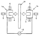
- two plasma sources 1a and 1b are arranged to face each other, and a sheet-like film forming target W is arranged between the plasma sources 1a and 1b. May be configured. At this time, if the front and back surfaces of the sheet-shaped film formation target W are arranged so as to face the plasma sources 1a and 1b, both surfaces of the film formation target W that is the film formation target are formed simultaneously. Note that a single-phase AC power supply 15 may be connected between the two plasma sources 1a and 1b.
- the direction of the magnetic poles of the magnets 5 and 6 provided in one plasma source 1a is opposite to the direction of the magnetic poles of the magnets 5 and 6 provided in the other plasma source 1b. Orientation is acceptable. By doing so, the lines of magnetic force are connected between the plasma sources 1a and 1b to suppress the diffusion of the lines of magnetic force. As a result, the plasma is efficiently guided to the film formation target W and the film formation efficiency is improved.
- a counter magnet may be arrange
- the direction of the magnetic pole of the counter magnet is the same as the direction of the magnetic pole of the back magnet 5 of the plasma source 1a.
- a plurality of plasma sources may be arranged along the side wall 10A of the vacuum chamber.
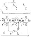
- three plasma sources 1a to 1c are arranged vertically in an adjacent state. If the plasma sources 1a to 1c are arranged in this way, film formation is performed at once on a wide area of the film formation target W.
- opposed magnets 19a to 19c respectively facing the plasma sources 1a to 1c are provided with a sheet-shaped film formation target W interposed therebetween.
- the counter magnets 19a to 19c are arranged so that the magnetic poles are oriented in the same direction as the magnetic poles of the back magnet 5 of the plasma sources 1a to 1c.
- the three plasma sources 1a to 1c may be arranged so as to surround the film formation target W. At this time, if the plasma sources 1a to 1c are arranged toward the film formation target W, the film formation is performed simultaneously on the entire outer peripheral surface of the film formation target W.
- the output terminals of the three-phase AC power supply 16 may be connected to each of the three plasma sources 1a to 1c shown in FIG. 12 or FIG. 13, and a three-phase AC potential may be applied to each plasma source 1a to 1c.
- the number of plasma sources is two or three, but may be one, or may be four or more.
- at least one of the back magnet 5, the outer peripheral magnet 6 and the counter magnet 19 may be an electromagnet.
- the “direction of the magnetic pole” means a direction in which magnetic lines of force exit from the electromagnet.
- the cathode 4 of the plasma source 1 may be surrounded by a case 17 having an opening 17 a on the front side of the cathode 4.
- the case 17 is disposed between the back magnet 5 and the outer peripheral magnet 6 and the cathode 4.
- the cathode 4 of the plasma source 1 may be surrounded by a case 18 having an opening 18 a on the front side of the cathode 4 together with the back magnet 5 and the outer peripheral magnet 6.
- cases 17 and 18 are normally connected to the ground potential, but may be connected to other potentials. Further, nozzles (throttle members) 17b and 18b may be provided as separate members around the openings 17a and 18a. Furthermore, the material of the cases 17 and 18 is usually a metal, but may be an insulator.
- the shape of the film formation target may be a plate shape or a curved surface in addition to a long film or sheet. Further, the film formation target may be various parts. In addition, the material to be deposited in the present invention may be a metal other than plastic.
- the plasma source according to the above embodiment is a plasma source that irradiates plasma, and has a cathode having a hollow portion surrounding a space where a magnetron discharge is generated, and a side opposite to the plasma irradiation direction with respect to the cathode. And a peripheral magnet that intermittently or continuously surrounds the cathode from a direction orthogonal to the plasma irradiation direction.
- the hollow portion opens at the front surface of the cathode, which is the surface on the plasma irradiation direction side, and faces the magnetic pole of the portion of the back magnet facing the cathode and the cathode of the outer peripheral magnet.
- the magnetic pole of the part is equal.
- the back magnet and the outer periphery magnet of the above embodiment are arranged such that the direction of the magnetic poles (the direction from the S pole to the N pole in the magnet) is directed to the cathode side or back to the cathode. ing.
- the generated lines of magnetic force are as follows.
- the cathode material When the cathode material is sputtered by the magnetron discharge, the ratio of the sputtered surface (part) in the normal direction increases in the flight direction of the cathode material. That is, the cathode material sputtered on the bottom wall surface of the hollow part flies so that the ratio toward the cathode front side (opening side), which is the normal direction of the bottom wall surface, increases, and is sputtered on the inner side surface of the hollow part. The cathode material flies so that the ratio toward the inner side surface opposite to the inner side surface, which is the normal direction of the inner side surface, increases.
- the proportion of the endless track region near the bottom wall surface of the hollow portion decreases and the ratio of the endless track region near the inner side surface of the hollow portion increases, the amount of cathode material flying to the front side of the cathode due to sputtering decreases. .
- the cathode material is less likely to flow out of the hollow portion (plasma source) through the opening, and excessive consumption of the cathode (cathode) and contamination of the cathode material (cathode constituent material) into the processing target are suppressed.
- the divergence of magnetic field lines from the plasma source to the film formation target is reduced, and the magnetic flux density of the magnetic field from the plasma source toward the film formation target is increased.
- the plasma is guided to the film formation target located at a position away from the plasma source by the magnetic field.
- the plasma concentration in the film formation target is increased, the film formation rate is increased and the productivity is increased.
- the magnetic flux density in the hollow portion is high, the plasma source can generate plasma even when the periphery of the cathode (for example, in the vacuum chamber) is at a relatively low pressure, and this plasma source is used in the film forming apparatus. In this case, production efficiency and convenience are improved.
- a plasma source specifically having the following configuration can be adopted.
- the hollow portion of the cathode has a shape such that the inner side surfaces facing each other in a cross section along the plasma irradiation direction are substantially parallel to each other, and the backside magnet and the outer peripheral magnet have magnetic lines of force passing near the inner side surface. It arrange
- the magnetic field lines passing through the vicinity of the inner side surface of the hollow portion of the cathode are substantially parallel to the inner side surface, so that the ratio of the vicinity of the bottom wall surface of the hollow portion in the endless track region substantially disappears and follows the inner side surface of the hollow portion.
- the ratio increases.
- substantially parallel includes not only the case of being completely parallel but also the case where the degree of parallelism is slightly deviated. Although it is desirable to be completely parallel, even if the parallelism is deviated by several degrees, the above-described effects can be achieved without problems.
- the hollow portion of the cathode of the above embodiment has a long groove shape extending in a direction orthogonal to the plasma irradiation direction.
- the hollow portion of the cathode has a shape in which a portion opened in a cross section along the plasma irradiation direction is narrower than a portion inside the opening.
- the hollow portion has a shape in which the opening portion is narrower than the inside thereof, so that the space necessary for magnetron discharge is secured in the hollow portion, and the cathode material flows out from the plasma source by the opening portion. Can be effectively prevented. Thereby, it is possible to prevent the film quality of the formed film from being deteriorated due to the mixed out cathode material.
- an aperture member for reducing the aperture area may be provided in the opening portion of the cathode.
- the diaphragm member is provided as a separate member, it is easy to change the diaphragm amount, and the replacement work at the time of maintenance is also facilitated.
- the film forming apparatus includes the above-described plasma source and the film forming target so that the film formation target passes through the front side which is the plasma irradiation direction side of the plasma source with respect to the plasma source. And a transport unit that transports the object.
- the plasma since the plasma is guided by the magnetic field to the film formation target located at a position away from the plasma source, the plasma concentration in the film formation target is high, so that the film formation rate of the film increases. Productivity increases.
- the magnetic flux density in the hollow portion of the plasma source is high, the plasma source can generate plasma even when the periphery of the cathode (for example, in the vacuum chamber) is at a relatively low pressure, which improves production efficiency and convenience. Become.
- the cathode material is less likely to flow out of the hollow portion (plasma source) through the opening of the cathode, and excessive consumption of the cathode (cathode) and contamination of the cathode material (cathode constituent material) into the processing target can be suppressed. .
- the film forming apparatus includes a counter magnet disposed so as to face the plasma source with a film forming object transferred to the transfer unit interposed therebetween, and the counter magnet has a magnetic pole at an end portion on the plasma source side. May be arranged so as to be opposite to the magnetic poles of the portion of the back magnet facing the cathode.
- the density of magnetic flux lines from the plasma source to the film formation target becomes higher, and as a result, the plasma is efficiently guided to the surface of the film formation target and the film formation efficiency is improved. More improved.
- the plasma source according to the present invention and the film forming apparatus including the plasma source are useful for forming a film on an object having various shapes, and the generated plasma is more distant from the plasma source. And is suitable for making the cathode material difficult to flow out of the plasma source.
Landscapes
- Chemical & Material Sciences (AREA)
- Engineering & Computer Science (AREA)
- Physics & Mathematics (AREA)
- Plasma & Fusion (AREA)
- Analytical Chemistry (AREA)
- Chemical Kinetics & Catalysis (AREA)
- Materials Engineering (AREA)
- Mechanical Engineering (AREA)
- Metallurgy (AREA)
- Organic Chemistry (AREA)
- Spectroscopy & Molecular Physics (AREA)
- Electromagnetism (AREA)
- Plasma Technology (AREA)
- Chemical Vapour Deposition (AREA)
Abstract
プラズマを照射するプラズマ源であって、マグネトロン放電が生じる空間を囲う中空部を有するカソードと、前記カソードに対して背面側に配置される背面磁石と、プラズマの照射方向と直交する方向からカソードを断続又は連続に取り囲む外周磁石とを備え、中空部は、カソードにおけるプラズマの照射方向側の面である前面で開口し、背面磁石及び外周磁石のカソードと対向する部位の磁極がすべて同極であることを特徴とするものである。
Description
本発明は、フィルム、シート、板状または曲面のパーツなどのさまざまな形状の成膜対象物に成膜する際に用いられるプラズマ源、及びこのプラズマ源を用いて成膜を行う成膜装置に関するものである。
従来、プラズマがフィルムなどの成膜対象物に照射されつつ、HMDSO(ヘキサメチルジシロキサン)などの原料ガスが前記プラズマに供給され、この原料ガスが当該プラズマによって分解されることによりSiOxCyなどの組成物が成膜対象物上に堆積する成膜処理が知られている。特許文献1は、前記成膜処理において用いられるプラズマ源が開示されている。また、特許文献2及び3には、プラズマ源と類似した構造を有し、プラズマを発生させるスパッタ電極が開示されている。
特許文献1に記載されたプラズマ発生源は、中空部を有するカソードと、前記中空部内にマグネトロン放電領域を形成すべく、カソードの側面を全周にわたって囲む磁石と、前記磁石の側面と前記カソードの側面及び背面とを覆うヨークと、を備える。前記カソードの中空部は、カソードの正面(成膜対象物と対向する面)で開口している。
特許文献2に記載されたスパッタ電極は、スパッタ装置においてプラズマを発生させるためのマグネトロンスパッタ電極である。この電極は、開口に向かって断面積が大きくなるように形成された中空部を備えたターゲット(陰極)と、このターゲットの背面(前記開口が設けられた面と反対側の面)に配置された背面磁石と、この磁石及びターゲットの側面及び背面を覆うヨークとを有している。
この構成によれば、ターゲットの中空部における内側側面の全周に亘ってマグネトロン放電が発生し、ターゲットから放出された放出電子が中空部内に効率よく閉じこめられる。これにより、プラズマ生成ガスのガス圧を下げることができ、プラズマ濃度が高くなる。
また、特許文献3に開示されたスパッタ装置は、中空部内においてプラズマを発生させる。このスパッタ装置は、中空部を有するターゲットと、このターゲットの側面を全周にわたって囲む磁石と、を有する。前記中空部は、カソードの正面で開口する。前記磁石は、S極からN極に向かう向きが成膜対象物に向かうように配置されている。
上述のように、成膜対象物に対する成膜処理に関して、プラズマを発生させるプラズマ発生源が種々提案されている。しかし、これらのプラズマ発生源は、中空部から外部に延びる磁力線が少ない等の理由により、プラズマを成膜対象物に向かって遠方まで導くことができないという問題を有する。
例えば、特許文献1のプラズマ発生源では、ヨークが磁力線の大部分をプラズマ源内に閉じ込める。このため、前記プラズマ発生源では、プラズマ源から離れた成膜対象物の近傍において十分な磁束密度が得られず、遠方の成膜対象物に対しては十分な成膜が行われない可能性がある。
また、特許文献2に記載されたスパッタ電極では、背面磁石のN極から出た磁力線は、中空部を通過したのちヨークを介して背面磁石のS極に戻る。このとき、N極から出た磁力線の一部は、中空部を通過する前からカソードの側面方向に広がって発散している。このため、成膜対象物における磁束密度は、特許文献1と同様に大きくならない。
また、特許文献3に記載されたスパッタ装置は、磁力線が成膜対象物側に指向されず、これにより、プラズマを遠方にまで照射できない。
すなわち、特許文献1~特許文献3のプラズマ発生源およびスパッタ電極は、離れた位置の成膜対象物近傍において十分な大きさの磁束密度が得られる磁場を形成することができず、これにより、プラズマを遠方の成膜対象物まで導けない。
さらに、特許文献2及び3のスパッタ電極は、プラズマをターゲット(カソード)に衝突させてターゲット物質を積極的に飛ばすスパッタ装置に用いられるものである。このため、前記スパッタ電極は、カソードから飛び出したターゲット物質を外部へ流出させる構造(ターゲット物質が外部に飛び出やすい構造)となっている。
それゆえ、特許文献2、3のスパッタ電極には、遠方にまでプラズマを照射させにくいという問題に加えて、陰極(カソードやターゲット)を構成する物質がプラズマ発生源から外側へ流出しやすいために、陰極が消耗しやすく、かつ処理対象に陰極を構成する物質が混入しやすいという問題もあった。
本発明の目的は、発生したプラズマをプラズマ源からより遠方まで導くことができ、且つ、カソード物質が流出し難いプラズマ源及びこのプラズマ源を用いた成膜装置を提供するものである。
本発明の一つの面によれば、プラズマを照射するプラズマ源であって、マグネトロン放電が生じる空間を囲う中空部を有するカソードと、前記カソードに対して前記プラズマの照射方向と反対の側である背面側に配置される背面磁石と、前記プラズマの照射方向と直交する方向から前記カソードを断続又は連続に取り囲む外周磁石と、を備える。そして、前記中空部は、前記カソードの前記プラズマの照射方向側の面である前面で開口し、前記背面磁石及び前記外周磁石の前記カソードと対向する部位の磁極がすべて同極である。
以下、本発明に係るプラズマ源及びこのプラズマ源を備えた成膜装置の実施形態を、図面を基に説明する。
なお、以下の説明では、同一の部品には同一の符号が付されている。同一の符号が付された部品同士は、名称及び機能が同じである。したがって、それらについての詳細な説明は繰り返さない。
本実施形態に係る成膜装置は、例えば図1に示すような、フィルムやシート状の成膜対象物Wに連続的に成膜する所謂ロールコーターである。
この成膜装置2は、真空チャンバ10と、アンコイラー11と、コイラー12と、搬送部と、複数(本実施形態では3つ)のプラズマ源1a~1cと、を備える。
真空チャンバ10は、内部が空洞とされた筐体である。真空チャンバ10は、気密構造となっていて、図示しない真空排気手段によって内部が減圧され真空状態若しくは真空に近い状態となっている。この真空チャンバ10は、その内部に、アンコイラー11と、コイラー12と、成膜ローラ13と、複数のプラズマ源1a~1cとを有する。
アンコイラー11は、コイル状の成膜対象物Wを巻き出し、コイラー12は、成膜後の成膜対象物Wを巻き取る。
搬送部は、複数の搬送ローラ20、20、…と、成膜ローラ13とを備え、アンコイラー11が巻き出した成膜対象であるシート状の成膜対象物Wをコイラー12まで搬送する。また、搬送部は、成膜対象物Wが各プラズマ源の前面側(プラズマの照射方向側)を通過するように成膜対象物Wを搬送する。
成膜ローラ13は、その軸心を水平方向(図1では紙面貫通方向)に向けるようにして配置されている。
複数の搬送ローラ20、20、…は、アンコイラー11からコイラー12までの搬送途中の成膜対象物Wが成膜ロール13に巻き掛けられるように配置されている。
複数のプラズマ源1a~1cは、成膜ロール13の側方であって、当該成膜ロール13と真空チャンバ10の側壁との間に配置されている。本実施形態では、図1において、右側に1つのプラズマ源1cが配置され、左側に2つのプラズマ源1a、1bが配置されている。各プラズマ源1a~1cは、プラズマを照射する開口が成膜ロール13の表面に対向するように、それぞれ配置されている。即ち、各プラズマ源1a~1cは、前記開口を成膜ロール13に巻き掛けられた成膜対象物Wに向けた姿勢となるように配置される。
本実施形態のように、2つのプラズマ源1a、1bが成膜ロール13に巻き掛けられた成膜対象物Wに沿って並べて設けられることにより、成膜対象物Wの広範囲に対して一度に成膜を行うことが可能となる。
この右方のプラズマ源1cは、図略のプラズマ電源の一方の電極に接続され、このプラズマ電源の他方の電極は、真空チャンバ10などに接続されている。一方、左方のプラズマ源1a、1bは、一つの交流電源(プラズマ電源)15に接続されている。具体的には、この交流電源15は単相交流の電源であって、一方の電極が一方のプラズマ源1aに接続され、他方の電極が他方のプラズマ源1bに接続されている。
所定の電圧が各プラズマ電源からプラズマ源1a~1cに印加されると、各プラズマ源1a~1cにおいてグロー放電が発生し、電離された原料ガスのプラズマが成膜対象物Wの表面に照射されてCVD皮膜が成膜される。
次に、プラズマ源1a~1cについて説明する。各プラズマ源1a~1cは、それぞれ同じ構成であるため、1つのプラズマ源(例えば1a)について説明し、他のプラズマ源(例えば、1b、1c)についての説明を省略する。尚、以下の説明では、プラズマ源の符号を1とする。
プラズマ源1は、成膜装置2に備えられ、例えばフィルムやシートなどの帯状基材(成膜対象物W)に対してCVD皮膜などを成膜するためのプラズマを発生させる。このプラズマ源1は、図2(a)~図3に示すように、カソード4と、背面磁石5と、外周磁石6とを有している。
以降の説明において、図2(b)において矢印xで示される方向が、プラズマ源1を説明する際の前方または前面側、矢印xの逆方向が後方または後面側(背面側)である。また、図2(a)において矢印yで示される方向が、プラズマ源1を説明する際の右側、矢印yの逆方向が左側である。さらに、図2(a)及び図2(b)において矢印zで示される方向が、プラズマ源1を説明する際の上側、矢印zの逆方向が下側である。
カソード4は、プラズマを発生させるのに必要なマグネトロン放電を表面近傍で起こすための電極(陰極)である。カソード4は、左右方向の幅寸法に比べて上下方向の長さ寸法が大きく、その前面が前方に向かって長方形状に開口している箱状の電極である。この開口の長手方向の寸法は、成膜対象物Wに対応する。そして、このカソード4は、その内部にマグネトロン放電が生じる空間(放電空間)を囲う中空部3を有する。
中空部3は、上下方向、すなわちカソード4の長手方向に沿って、カソード4の前面から後面側に凹む長尺の溝状の部位である。中空部3は、上下方向に延び且つ前方を向く底壁面41と、この底壁面41の周縁から前方に向かって伸びる側壁面(内側側面)42とを有する。即ち、放電空間は、底壁面41と、側壁面42とによって囲まれている。
この中空部3は、前面側が開放状態となるように放電空間を囲い、この放電空間内に酸素などのプラズマ生成用ガスを供給可能に構成される。これにより、プラズマ生成用ガスが中空部3に囲まれた放電空間において生じたマグネトロン放電によって電離状態となり、プラズマ生成用ガスのプラズマが放電空間において生起される。このマグネトロン放電では、カソード4から中空部3内に放出された電子が、後述する背面磁石5と外周磁石6とが形成する磁場によって、カソード4の底壁面41及び側壁面42の近辺(無限軌道領域14内)で周回し続ける。
カソード4は、中空部3において生成されたプラズマ生成用ガスのプラズマ(本実施形態では酸素プラズマ)を成膜対象物側に向かって照射する。これにより、成膜装置2では、図示しない供給部から供給されるHMDSOなどの原料ガスのプラズマが発生する。
カソード4の前面の開口は、成膜対象物Wに対応した幅を有するスリット状の開口である。これにより、カソード4は、成膜対象物Wに対してライン状にプラズマを照射できる。
また、図2(b)及び図3において矢印xによって示される方向、つまりプラズマ源1の前方方向であるプラズマの照射方向に沿った断面において、中空部3を形成する側壁面42のうち、上面42Uと下面42Bとは互いに平行な平面状に形成されている。また、左側面42Lと右側面42Rも互いに平行な平面状に形成されている。そして、後述するように、プラズマの軸線(照射方向)は、本願発明の特徴である背面磁石5及び外周磁石6の取り付け方向と磁極の向きとによって、側壁面42に平行となるように、即ち、4つの壁面42U、42B、42L、42Rのいずれとも平行となるように設定されている。
カソード4の前面の開口形状、即ち、前面側から見た側壁42の形状が長方形であるので、中空部3の側壁面42に沿って周回し続ける上述のマグネトロン放電における無限軌道領域は、図2において符号14によって示すように、一辺が特に長い長方形の環状となる。背面磁石5及び外周磁石6が形成する磁場の磁力線に沿って、上記の長尺の環状の無限軌道領域14において発生したプラズマがカソード4の前面の開口を通じて外部に引き出される。これにより、前記引き出されたプラズマは、シート状となる。
なお、中空部3は、カソード4の前面の開口部分が中空部3の内側の幅よりも狭い幅となるように形成されてより狭い(細い)スリット状となるような形状を有していてもよい。これによって、中空部3内においてマグネトロン放電に必要な放電空間の大きさが確保されつつより細く均一なシート状(スリット状)のプラズマが照射可能なプラズマ源が実現される。
背面磁石5は、カソード4の背面側(後方)に配置される。本実施形態の背面磁石5は、カソード4の背面側に当該カソード4から距離をあけて配置される。背面磁石5は、例えば、永久磁石である。この背面磁石5は、上下方向に伸びる棒状(本実施形態では角棒形状)の磁石7を前後方向に複数本(本実施形態では5本)重ね合わせたものである。各磁石7の前後方向(x方向)、左右方向(y方向)、上下方向(z方向)の寸法は、カソード4の中空部3(の内寸)よりそれぞれ小さい。本実施形態の背面磁石5は、5本の棒状の磁石7を重ね合わせることにより、棒状の磁石7が1本だけの場合に比べ、形成される磁場の磁束密度を高めている。
外周磁石6は、カソード4の外周を取り囲むように配置される。具体的に、外周磁石6は、プラズマの照射方向と直交する方向からカソード4を断続又は連続に取り囲む複数の磁石を有する。本実施形態の外周磁石6は、4つの磁石6U、6B、6L、6Rを有する。尚、外周磁石6は、1つの磁石によって構成されてもよい。
詳しくは、外周磁石6は、カソード4の上側の外壁面から上方に離れた位置に設けられる上側の磁石6U、カソード4の下側の外壁面から下方に離れた位置に設けられる下側の磁石6B、カソード4の左側の外壁面から左方に離れた位置に設けられる左側の磁石6L、及びカソード4の右側の壁面から右方に離れた位置に設けられる右側の磁石6Rの4つの磁石を有する。これら4つの磁石6U、6B、6L、6Rの外形形状は、いずれも直方体状または板状である。
上側の磁石6Uの左右方向(y方向)の幅は、カソード4と略同じ、又はやや短い。また、この磁石6Uの前後方向(x方向)の奥行きは、カソード4と略同じ、又はやや短い。さらに、この磁石6Uの上下方向(z方向)の長さは、背面磁石5の左右方向(y方向)の幅と略同じ、又はやや短い。そして、下側の磁石6Bは、この上側の磁石6Uと全く同じ外形形状である。
右側の磁石6Rの上下方向(z方向)の長さは、カソード4と略同じ、又はやや短い。また、この磁石6Rの前後方向(x方向)の奥行きは、カソード4と略同じ、又はやや短い。さらに、この磁石6Rの左右方向(y方向)の幅は、背面磁石5と略同じ、又はやや短い。そして、左側の磁石6Lは、この右側の磁石6Rと全く同じ外形形状である。
これら4つの磁石6U、6B、6L、6Rは、いずれもカソード4の外周の表面から磁石の厚みよりやや狭い間隔だけ距離を取って配置されている。
ところで、本実施形態のプラズマ源1は、上述した背面磁石5及び外周磁石6の取り付け方向と磁極の向きとに特徴を備えている。この特徴的な背面磁石5及び外周磁石6の取り付け方向と、磁極の向きと、が適切に選択されることに加え、更に、磁石の形状と、磁力(磁束密度)の大きさと、が適切に選択されることによって、カソード4の中空部3の側壁面42付近を通る磁力線が中空部3の4つの壁面42U、42B、42L、42Rのいずれとも平行ないしほぼ平行となる。つまり、前記特徴は、背面磁石5のカソード4と対向(対面)する部位の磁極と、外周磁石6におけるカソード4と対向する部位の磁極が等しい(同極となっている)点である。これにより、各磁石5、6における磁極の向きがカソード4側を向くか、あるいはカソード4側に対して背向する。
ここで、「磁極の向き」は、磁石において「S極からN極へ向かう方向」のことであり、図2(a)~図3において矢印Fによって表わされる向きである。この磁極の向きは、各磁石のN極における磁力線の向きを示している。さらに、この「磁極の向きF」がカソード4側を向く、又は背向するとは、磁極の向きFを延長した直線とカソード4の外壁面とが垂直乃至は略垂直に交わることである。
本実施形態では、図2に示す如く、背面磁石5のカソード4に対面(対向)する部位の極(磁極)は、N極である。また、外周磁石6を構成する4つの磁石6U、6B、6L、6Rに関しても、カソード4に対面(対向)する部位の磁極はそれぞれN極である。言い換えるならば、背面磁石5の磁極の向きFは、カソード4を指向し、外周磁石6を構成する4つの磁石6U、6B、6L、6Rの磁極の向きもそれぞれカソード4を指向する。
なお、背面磁石5と外周磁石6との磁極の向きが反対方向を向く場合にも、上述した本発明の特徴を満足させる。例えば、背面磁石5のS極がカソード4に対面し、且つ、外周磁石6を構成する4つの磁石6U、6B、6L、6RのS極がすべてカソード4と面していれば、各磁石5、6U、6B、6L、6Rの磁極の向きFはカソード4に対してそれぞれ背向することとなり、上述した本発明の特徴を満足する。
次に、これら背面磁石5及び外周磁石6の取り付け方向と磁極の向きとの関係を、詳しく説明する。
例えば、図4は、本実施形態のカソード4の前面に開口面積を絞るための絞り部材8が取り付けられた状態で、背面磁石5のみが設けられたプラズマ源(後述する比較例1)の磁力線分布図である。図4に示すように、このプラズマ源では、背面磁石5のN極が前方、S極が後方を向いていて、背面磁石5の磁極の向きはカソード4を向いている。しかしながら、図4に示すプラズマ源には、外周磁石6が設けられていないので、上述した本発明の特徴が満たされない。図4のプラズマ源では、カソード4の後面側に配置された背面磁石5のN極から出た磁力線は、中空部3内(放電空間)に達するまでに拡散する。このため、プラズマ源の前方に配置された成膜対象物Wでの磁束密度は、あまり高くない。なお、図4は、Z=0mm平面における磁力線の分布を示している。
図5は、本実施形態のカソード4の前面に絞り部材8が取り付けられた状態で、外周磁石6Aのみが設けられたプラズマ源(後述する比較例2)の磁力線分布図である。図5に示すように、外周磁石6を構成する4つの磁石は、N極を後方に向け且つS極を前方に向けてそれぞれ配置されている。この場合、外周磁石6Aを構成する各磁石の磁極は、カソード4と対面しておらず、前記各磁石の磁極の向きは、後方を向いていてカソード4を指向していない。この場合、カソード4内の放電空間を通る磁力線は、プラズマ源から前方に出て行くことはなく、カソード4及び絞り部材8を貫通して外周磁石6Aに戻る。このため、当該プラズマ源では、カソード4の内部から直接成膜対象物Wに向かう磁力線は存在しない。
一方、図6は、本実施形態のカソード4の前面に絞り部材8が取り付けられた状態で、背面磁石5と外周磁石6の両方が設けられたプラズマ源1A(後述する実施例1)の磁力線分布図である。図6に示すプラズマ源1Aでは、前述した如く、背面磁石5はN極が前方を向き、S極が後方を向くように配置される。また、外周磁石6を構成する各磁石は、N極がカソード4に対面し、S極がカソード4の外側を向くようにそれぞれ配置される。
このように、全ての磁石の磁極の向きがいずれもカソード4側を向くように、背面磁石5と外周磁石6とが配置されれば、カソード4内の放電空間では、発散が少なく且つ中空部3の側壁面42と平行に近い磁力線分布となって磁束密度が高くなる。また、プラズマ源1Aからその前方に配置された成膜対象物Wまでの間においても、磁力線の発散の少ない磁力線分布となるため、成膜対象物Wの近傍でのプラズマ源1Aから成膜対象物Wへ向かう磁束線の密度(即ち、磁束密度)が高くなる。
このように背面磁石5と外周磁石6とが同じ磁極をカソード4側に向けてそれぞれ配置されれば、カソード4の中空部3内の放電空間近傍では、発散が少なく且つカソード4の側面壁42と平行に近い磁力線分布となり、磁束密度が高くなる。また、プラズマ源1Aからその前方に配置された成膜対象物Wまでの間においても、磁力線の発散の少ない磁力線分布となるため、成膜対象物Wの近傍でのプラズマ源1Aから成膜対象物Wへ向かう磁束線の密度(即ち、磁束密度)が更に高くなる。これにより、放電空間で生じたプラズマが成膜対象物Wまで更に効率よく導かれる。さらに、放電空間において磁力線がカソード4の側壁面42と平行に近いため、マグネトロン放電の無限軌道領域14(カソード4から中空部3内に放出された電子が磁場によって高密度で周回する領域)おける中空部3の底壁面41付近の割合が減少するとともに、中空部3の側壁面42(上下左右の面42U、42B、42L、42R)付近の割合が増加する。カソード4の底面付近における無限軌道領域14が減少すれば、カソード4の底面からカソード4の前面側へスパッタされるカソード物質が少なくなる。このため、カソード物質がプラズマ源1Aの外部へ流出することを防止できる。これにより、流出したカソード物質が成膜した皮膜に混入することによる前記皮膜の膜質の低下が防止される。
次に、図7は、本実施形態のカソード4の前面に絞り部材8が取り付けられた状態で、背面磁石5と外周磁石6Bとの両方が設けられた他のプラズマ源1B(後述する実施例2)の磁力線分布図である。図7に示すプラズマ源1Bは、本実施形態の外周磁石6よりも厚みを増やした外周磁石6Bが用いられることにより、図6に示した外周磁石6よりも磁力を強力にした。
なお、カソード4は、上述したようにカソード4の前面の開口そのものが狭いスリット状となるように構成されなくてもよい。カソード4は、図4~図7に示すように、溝状の中空部3が形成されたカソード4と、カソード4の開口の開口面積を絞る絞り部材8とを備えてもよい。この絞り部材8は、カソード4の前面の開口よりも開口幅の狭い(開口面積を絞った)スリット状の開口を有して中空部3の前方に配置される。この場合、絞り部材8は、カソード4の中空部3の前方に当該カソード4から距離をあけて配置されてもよい。
図6及び図7に示すように、この絞り部材8は、前後方向に沿ってスリット状に貫通した開口部9を備えている。この絞り部材8の開口部9は、プラズマの照射方向に沿った断面において、中空部3において対向する壁面42L、42R同士の間隔よりも狭い幅となるように形成されており、カソード4の前面の開口より小さい開口面積を備えている。絞り部材8は、カソード4とは電気的に接続されておらず、カソード4の電位(カソード電位)と異なる電位にしてもよい。
このような絞り部材8が設けられれば、カソード4を構成する物質(カソード物質)が中空部3から放出された場合であっても、この物質がプラズマ源1のさらに外部に流出することが防止される。これにより、カソード4から流出したカソード物質が成膜した皮膜に混入することにより当該皮膜の膜質が低下することが防止される。また、絞り部材8がカソード4と別部材とされることにより、開口部9の形状が絞り部材8の取り替えによって容易に変更される。このため、開口部9の形状を成膜対象物Wの形状に容易に合わせることができる。
次に、本発明のプラズマ源1の作用効果を、シミュレーション計算の結果(実施例1,実施例2)を用いて、さらに詳しく説明する。
実施例1,2及び比較例1,2のシミュレーションは、高さ350mm×幅25mm×奥行30mmの中空部3を備えたプラズマ源に関するものである。図8、9は、このプラズマ源からの水平距離に応じて磁束密度がどのように変化するかを計算した結果を示す。
なお、各プラズマ源に用いられる背面磁石5は、残留磁束密度が1.35[T]の板状の磁石(高さ350mm×幅10mm×厚み10mm)を5枚重ね合わせたものである。この背面磁石5は、カソード4の後面から後方に5mmの距離だけ離れた位置に配置されている。また、外周磁石6は、カソード4の上外側面、下外側面、左外側面、右外側面からいずれも15mmの距離だけ離れた位置に配置された4つの板状の磁石により構成される。いずれの磁石も残留磁束密度が1.195[T]の磁力を備えている。
図4に示す比較例1は、カソード4の後面側に背面磁石5だけが設けられていて、外周磁石6が設けられていない。図5に示す比較例2は、カソード4の外周側に外周磁石6Aだけが設けられていて、背面磁石5が設けられていない。なお、比較例2では、外周磁石6Aの取り付け方向は、磁極の向きが前後方向に向くように配置されていて、実施例1、2のように磁極の向きFがカソード4に向いていない。
一方、実施例1は、図6に示すような磁石配置を有する。具体的に、背面磁石5と外周磁石6とは、N極がカソード4に対面するようにそれぞれ配置されている。図7の実施例2は、外周磁石6Bの厚みを実施例1の外周磁石6の3倍にしている。
なお、前後方向(x方向)、左右方向(y方向)、上下方向(z方向)が各実施例及び各比較例の説明において使用されているが、この座標系の原点は、背面磁石5を構成する5枚の板状の磁石のうち、最もカソード4側に配備された板状の磁石の中心位置を基準として定められている。
図4に示す比較例1では、背面磁石5のN極から出た磁力線が中空部3およびプラズマ源1の前方において広がって拡散している。このため、プラズマ源1の前方に配置された成膜対象物Wの位置における磁束密度は、実施例1、2のものほど高くはない。また、中空部3内(放電空間内)の磁力線の多くが、カソード4の底壁面41から側壁面42に向かっているため、マグネトロン放電において電子が磁場によって閉じ込められる位置(無限軌道領域)は、図4の14に示されるようにカソード4の底壁面41と側壁面42との境界付近となる。
また、図5に示す比較例2では、カソード4の中空部3内を通る磁力線がプラズマ源1から前方に出て行くことはなく、カソード4と絞り部材8とを貫通して外周磁石6Aに戻っている。このため、カソード4の中空部3内から成膜対象物Wに直接向かう磁力線は存在しない。
しかしながら、図6に示す実施例1では、比較例1に対して外周磁石6が追加されているため、中空部3内の側壁面42付近の磁力線が、側壁面42と平行に近くなり、しかも磁束密度が急増し、これにより、中空部3内ではより強力なマグネトロン放電が起こり、電子の閉じこめ効率が急増する。また、外周磁石6が追加されることによって、比較例1及び比較例2と比較して、中空部3から前方に延びる磁力線の発散が少なくなり、プラズマ源から成膜対象物Wに向かう磁力線の密度(磁束密度)も高くなる。これによって、中空部3内において生じた多くのプラズマが磁力線に沿ってプラズマ源1から離れた遠方まで導かれる。また、中空部3内の磁力線が中空部3の側壁面42と平行に近くなっているので、マグネトロン放電において電子が磁場によって閉じ込められる位置(無限軌道領域)は、図6の14に示す位置となる。即ち、図4の比較例に比べて無限軌道領域14における中空部3の側壁面42付近の比率が増す。
次に、図7に示す実施例2では、図6に示す実施例1の外周磁石6と比較してより強い永久磁石(外周磁石6B)が用いられる。
この実施例2では中空部3内の磁力線が側壁面42とより平行になっているので、無限軌道領域14が、実施例1よりも更に広く、即ち、前後方向における側壁面42のほぼ全域に沿って形成される。言い換えると、無限軌道領域14の前後方向の幅が更に広くなる。また、中空部3内の側壁面42付近の磁束密度が更に増加する。その結果、電子の閉じ込め効率が更に良くなるため、更に低いガス圧でも動作する(プラズマを形成する)ことができ、無限軌道領域14におけるプラズマ密度が更に高くなる。
マグネトロン放電においては、中空部3の側壁面42での放電割合が更に増えると共に、開口部9に相対している中空部3の底壁面41での放電割合がほとんど無くなる。このため、カソード4の開口から前方に流出するスパッタ粒子(カソード物質)が激減する。
また、実施例2では、実施例1と比較して、中空部3から成膜対象物Wへ向かう磁力線の発散がより低減していることによって中空部3から成膜対象物Wへ向かう磁力線の数が更に増えている。このため、より多くのプラズマが磁力線に沿ってプラズマ源1Bから離れた遠方まで導かれる。
図8は、比較例1、実施例1、2のy=10mmの位置におけるx方向の各位置での磁束密度を計測した結果を示す。このy方向の位置は、y=12.5mmの位置にある側壁面42の右側の壁面42Rから2.5mmほど中空側である。従って、この位置での磁束密度が高ければ電子の閉じ込め効率がより良くなり、より低いガス圧でも動作することができる。これにより、無限軌道領域14におけるプラズマ密度がより高くなる。また、中空部3の底壁面41は、x=20mmの位置にあり、中空部3内の放電空間はx=20~50mmの範囲に存在する。中空部3の底壁面41近傍を除くほとんどの放電空間において、比較例1<実施例1<実施例2の順に磁束密度が高くなっており、電子の閉じ込め効率がより良くなる。このため、前記の順に、より低ガス圧で動作することができ、無限軌道領域14におけるプラズマ密度がより高くなることが分かる。
図9も、比較例1、実施例1,2のy=0mmの位置(すなわちカソード4の幅方向の中心)におけるx方向の各位置での磁束密度を計測した結果を示す。カソード4の中空部3からプラズマ源1の前方の所定位置(x=200mmの位置)までのすべての領域において、比較例1<実施例1<実施例2の順に磁束密度が高くなっている。このため、前記の順に、より多くのプラズマが磁力線に沿ってプラズマ源1から離れた遠方まで導かれることが分かる。
上記実施形態の成膜装置2のように、一方のプラズマ源1aに備えられた各磁石5、6の磁極の向きFと、他方のプラズマ源1bに備えられた各磁石5、6の磁極の向きFとが互いに反対向きであってもよい。かかる構成によれば、磁力線が両プラズマ源1a、1bの間でつながり、各プラズマ源1a、1bの前方側における磁力線の拡散がより抑えられる。これにより、プラズマが効率よく成膜対象物Wに導かれ、成膜効率が向上する。このときに、カソード4の中空部3内にプラズマ生成用のガスが導入されてもよい。このプラズマ生成用ガスの導入によって、CVD皮膜の成膜がより効果的に行われる。
また、図10に示すように、対向磁石50が、成膜対象であるシート状の成膜対象物Wを挟んでプラズマ源(例えば1c)と反対側の成膜ロール13の内部に設けられてもよい。この場合、対向磁石50は、その磁極の向きがプラズマ源1cの背面磁石5における磁極の向きと同方向となるように設けられる。これにより、プラズマ源1cから出た磁力線の拡散がより抑えられ、プラズマがより直線的に成膜対象である成膜対象物Wに導かれる。なお、対応磁石50は、成膜ロール13が回転しても、プラズマ源1cとの相対位置が変わらないように成膜ロール13内に設置されている。
また、成膜装置2は、図11に示すように、2つのプラズマ源1a、1bが対向して配置され、プラズマ源1a、1bの中間にシート状の成膜対象物Wが配置されるように構成されてもよい。このとき、シート状の成膜対象物Wの表面と裏面とがプラズマ源1a、1bに向くように配置すれば、成膜対象である成膜対象物Wの両面が、同時に成膜される。なお、この2つのプラズマ源1a、1bの間に単相交流の交流電源15が接続されてもよい。
さらに、図11に示すように、一方のプラズマ源1aに備えられた各磁石5、6の磁極の向きと、他方のプラズマ源1bに備えられた各磁石5、6の磁極の向きとが反対向きでもよい。このようにすることで、両プラズマ源1a、1bの間で磁力線がつながって磁力線の拡散が抑えられ、その結果、プラズマが効率よく成膜対象物Wに導かれて成膜効率が向上する。
なお、図11の他方のプラズマ源1bに代えて、対向磁石が配置されてもよい。この場合、対向磁石の磁極の向きは、プラズマ源1aの背面磁石5における磁極の向きと同じである。
さらに、図12に示すように、複数のプラズマ源が真空チャンバの側壁10Aに沿って配置されてもよい。図12の例では、3つのプラズマ源1a~1cが、隣接した状態で上下に並んでいる。各プラズマ源1a~1cがこのように配置されれば、成膜が成膜対象物Wの広範囲に対して一度に行われる。
なお、図12に示す例では、プラズマ源1a~1cに各々対向する対向磁石19a~19cが、シート状の成膜対象物Wを挟んで設けられている。この対向磁石19a~19cは、磁極の向きがプラズマ源1a~1cの背面磁石5における磁極の向きと同じ向きとなるように配置されている。こうすることにより、プラズマが成膜対象物Wの表面に効率的に導かれて成膜効率が向上する。
また、図13に示すように、3つのプラズマ源1a~1cが成膜対象物Wの周囲を囲むように配置されてもよい。このとき、各プラズマ源1a~1cが成膜対象物Wに向けて配置されれば、成膜が成膜対象物Wの外周面全面に対して同時に行われる。
図12または図13に示す3つのプラズマ源1a~1cの各々に3相交流電源16の出力端子が接続され、各プラズマ源1a~1cに3相交流電位が印加されてもよい。
図1、及び図11~図13では、プラズマ源の個数が2つ又は3つであるが、1つであってもよいし、4つ以上あってもよい。また、背面磁石5,外周磁石6および対向磁石19のうち少なくとも1つが電磁石であってもよい。電磁石が使用される場合、その「磁極の向き」とは、電磁石から磁力線が出て行く方向のことをいう。
さらに、図14に示すように、プラズマ源1のカソード4が、このカソード4の前面側に開口17aしたケース17によって囲まれてもよい。この場合、ケース17が、背面磁石5及び外周磁石6とカソード4との間に配置される。また、図15に示すように、プラズマ源1のカソード4が、背面磁石5および外周磁石6とともに、カソード4の前面側に開口18aしたケース18によって囲われてもよい。
これらのケース17、18は、通常アース電位に接続されるが、その他の電位に接続されてもよい。また、開口部17a、18aの周囲にノズル(絞り部材)17b、18bが別部材として設けられてもよい。さらに、ケース17、18の材質は、通常金属であるが、絶縁物でもよい。
成膜対象の形状は、フィルムやシートなどの長尺もの以外に、板状または曲面などでもよい。また、成膜対象は、各種パーツなどでもよい。また、本発明の成膜対象の材質は、プラスチック以外に、金属などでもよい。
なお、本発明は、上記各実施形態に限定されるものではなく、発明の本質を変更しない範囲で各部材の形状、構造、材質、組み合わせなどを適宜変更可能である。
[実施の形態の概要]
以上の実施形態をまとめると、以下の通りである。
以上の実施形態をまとめると、以下の通りである。
即ち、上記の実施形態に係るプラズマ源では、プラズマを照射するプラズマ源であって、マグネトロン放電が生じる空間を囲う中空部を有するカソードと、前記カソードに対して前記プラズマの照射方向と反対の側である背面側に配置される背面磁石と、前記プラズマの照射方向と直交する方向から前記カソードを断続又は連続に取り囲む外周磁石と、を備える。そして、前記中空部は、前記カソードにおける前記プラズマの照射方向側の面である前面で開口しており、前記背面磁石の前記カソードと対向する部位の磁極と、前記外周磁石の前記カソードと対向する部位の磁極とが等しい。
言い換えるならば、上記実施形態の背面磁石及び外周磁石は、その磁極の向き(磁石内においてS極からN極へ向かう方向)がいずれもカソード側に向く、又はカソードに背を向けるように配置されている。このように、背面磁石及び外周磁石が同じ磁極をカソード側に向けて配置されれば、発生する磁力線は下記のようになる。
カソードの中空部近傍では磁束線の発散が少なく、各磁束線がプラズマの照射方向と平行に近くなるとともに、中空部における磁束密度が高くなる。その結果、カソードから中空部内に放出された電子が磁場によって中空部内を前記開口の周縁方向に周回する無限軌道領域に閉じ込められるマグネトロン放電において、前記無限軌道領域の中空部の底壁面(開口と対向する部位)付近の割合が減少するとともに、中空部の内側側面(プラズマの照射方向を囲む部位)付近の割合が増加し、そのプラズマ密度も増加する。マグネトロン放電によりカソード物質がスパッタされると、このカソード物質の飛行方向において、スパッタされた面(部位)の法線方向の比率が高くなる。つまり、中空部の底壁面においてスパッタされるカソード物質は、前記底壁面の法線方向であるカソード前面側(開口側)へ向かう比率が高くなるように飛行し、中空部の内側側面においてスパッタされるカソード物質は、内側側面の法線方向である当該内側側面と対向する内側側面へ向かう比率が高くなるように飛行する。つまり、中空部の底壁面付近の無限軌道領域の割合が減少し、中空部の内側側面付近の無限軌道領域の割合が増加すれば、スパッタによりカソードの前面側へ飛行するカソード物質の量が減る。これにより、カソード物質が開口を通じて中空部(プラズマ源)から流出しにくくなり、カソード(陰極)の過度な消耗と処理対象へのカソード物質(陰極構成物質)の混入とが抑えられる。
また、プラズマ源から成膜対象物までの間における磁力線の発散が少なくなり、プラズマ源から成膜対象物へ向かう磁場の磁束密度が高くなる。その結果、プラズマがプラズマ源から離れた位置にある成膜対象物まで前記磁場によって導かれるようになる。また、成膜対象物におけるプラズマ濃度が高くなるので、皮膜の成膜速度が大きくなり生産性が高くなる。また、中空部内の磁束密度が高くなるため、カソード周辺(例えば、真空チャンバ内)が比較的低圧な状態でもプラズマ源がプラズマを発生させることが可能となり、このプラズマ源が成膜装置に利用された場合、生産効率及び利便性が良くなる。
このようなプラズマ源としては、具体的に以下の構成を備えたものを採用することができる。
前記カソードの中空部は、前記プラズマの照射方向に沿った断面において対向する内側側面が互いに略平行となるような形状を有し、前記背面磁石及び外周磁石は、前記内側側面付近を通る磁力線が当該内側側面と略平行となるように配置されている。
このように、カソードの中空部の内側側面付近を通る磁力線が当該内側側面と略平行となることにより、無限軌道領域における中空部の底壁面付近の割合がほぼなくなり、中空部の内側側面に沿う割合が多くなる。このように、中空部の底壁面近傍でのマグネトロン放電が少なくなれば、中空部の底壁面からカソードの前面側へスパッタされるカソード物質が減少するので、カソード物質がプラズマ源の外部へ流出することがより抑制される。これにより、流出したカソード物質が混入して成膜した皮膜の膜質が低下することを防止することができる。
ここで、「略平行」とは、完全に平行な場合に加えて、多少平行度がずれている場合も含む。完全に平行であることが望ましいが、数度程度、平行度がずれていても、上述の作用効果が問題なく達成される。
上記実施形態の前記カソードの中空部は、前記プラズマの照射方向と直交する方向に延びる長尺の溝状であることが好ましい。
かかる構成によれば、プラズマが前記溝に対応するシート状に照射されるため、シートやフィルムのような帯状の成膜対象物、及び板状または曲面のパーツなどの幅のある成膜対象物が搬送されつつ成膜される場合に、広い範囲への成膜が容易に行われる。
また、前記カソードの中空部は、前記プラズマの照射方向に沿った断面において開口した部分が当該開口より内側の部分に比して狭くなるような形状を有することがより好ましい。
このように中空部がその内側よりも開口した部位が狭くなる形状を有することにより、マグネトロン放電に必要な空間を中空部内に確保しつつ、前記開口した部位によってカソード物質がプラズマ源から流出することを効果的に防ぐことができる。これにより、成膜した皮膜の膜質が流出したカソード物質の混入によって低下することを防止することができる。
上記実施形態のプラズマ源では、前記カソードの開口部分に、開口面積を絞る絞り部材が設けられてもよい。
このように、絞り部材が別部材として設けられることにより、絞り量を変更することが容易であり、さらにメンテナンスの際の交換作業も容易になる。
また、上記実施形態に係る成膜装置は、上述したプラズマ源と、成膜対象物が前記プラズマ源に対して当該プラズマ源のプラズマの照射方向側である前面側を通過するように当該成膜対象物を搬送する搬送部と、を有していることを特徴とする。
かかる構成によれば、プラズマがプラズマ源から離れた位置にある成膜対象物まで磁場によって導かれるようになるため、成膜対象物におけるプラズマ濃度が高くなるので、皮膜の成膜速度が大きくなり生産性が高くなる。また、プラズマ源の中空部内の磁束密度が高くなるため、カソード周辺(例えば、真空チャンバ内)が比較的低圧な状態でもプラズマ源がプラズマを発生させることが可能となり、生産効率及び利便性が良くなる。
しかも、プラズマ源においてカソード物質がカソードの開口を通じて中空部(プラズマ源)から流出しにくくなり、カソード(陰極)の過度な消耗と処理対象へのカソード物質(陰極構成物質)の混入とが抑えられる。
この成膜装置は、前記搬送部に搬送される成膜対象物を挟んで前記プラズマ源と対向するように配置された対向磁石を備え、前記対向磁石は、前記プラズマ源側の端部の磁極が前記背面磁石の前記カソードと対向する部位の磁極と逆になるように配置されてもよい。
このように対向磁石が配置されることによってプラズマ源から成膜対象物へ向かう磁束線の密度がより高くなり、これにより、プラズマが成膜対象物の表面により効率よく導かれて成膜効率がより向上する。
以上のように、本発明に係るプラズマ源及びこのプラズマ源を備えた成膜装置は、さまざまな形状の成膜対象物に成膜するのに有用であり、発生したプラズマをプラズマ源からより遠方まで導くことができ、且つ、カソード物質をプラズマ源から流出し難くするのに適している。
Claims (7)
- プラズマを照射するプラズマ源であって、
マグネトロン放電が生じる空間を囲う中空部を有するカソードと、
前記カソードに対して前記プラズマの照射方向と反対の側である背面側に配置される背面磁石と、
前記プラズマの照射方向と直交する方向から前記カソードを断続又は連続に取り囲む外周磁石と、を備え、
前記中空部は、前記カソードにおける前記プラズマの照射方向側の面である前面で開口しており、
前記背面磁石の前記カソードと対向する部位の磁極と、前記外周磁石の前記カソードと対向する部位の磁極とが等しいことを特徴とするプラズマ源。 - 前記カソードの中空部は、前記プラズマの照射方向に沿った断面において対向する内側側面が互いに略平行となるような形状を有し、
前記背面磁石及び外周磁石は、前記内側側面付近を通る磁力線が当該内側側面と略平行となるように配置されていることを特徴とする請求項1に記載のプラズマ源。 - 前記カソードの中空部は、前記プラズマの照射方向と直交する方向に延びる長尺の溝状であることを特徴とする請求項1に記載のプラズマ源。
- 前記カソードの中空部は、前記プラズマの照射方向に沿った断面において開口した部分が当該開口より内側の部分に比して狭くなるような形状を有することを特徴とする請求項1に記載のプラズマ源。
- 前記カソードの開口部分に、開口面積を絞る絞り部材が設けられていることを特徴とする請求項1に記載のプラズマ源。
- 請求項1~5のいずれかに記載されたプラズマ源と、
成膜対象物が前記プラズマ源に対して当該プラズマ源のプラズマの照射方向側である前面側を通過するように当該成膜対象物を搬送する搬送部と、を有していることを特徴とする成膜装置。 - 前記搬送部に搬送される成膜対象物を挟んで前記プラズマ源と対向するように配置された対向磁石を備え、
前記対向磁石は、前記プラズマ源側の端部の磁極が前記背面磁石の前記カソードと対向する部位の磁極と逆になるように配置されていることを特徴とする請求項6に記載の成膜装置。
Applications Claiming Priority (2)
| Application Number | Priority Date | Filing Date | Title |
|---|---|---|---|
| JP2011-048936 | 2011-03-07 | ||
| JP2011048936A JP5688996B2 (ja) | 2011-03-07 | 2011-03-07 | プラズマ源及びこのプラズマ源を備えた成膜装置 |
Publications (1)
| Publication Number | Publication Date |
|---|---|
| WO2012120850A1 true WO2012120850A1 (ja) | 2012-09-13 |
Family
ID=46797823
Family Applications (1)
| Application Number | Title | Priority Date | Filing Date |
|---|---|---|---|
| PCT/JP2012/001430 Ceased WO2012120850A1 (ja) | 2011-03-07 | 2012-03-02 | プラズマ源及びこのプラズマ源を備えた成膜装置 |
Country Status (2)
| Country | Link |
|---|---|
| JP (1) | JP5688996B2 (ja) |
| WO (1) | WO2012120850A1 (ja) |
Cited By (1)
| Publication number | Priority date | Publication date | Assignee | Title |
|---|---|---|---|---|
| JP2016513336A (ja) * | 2013-02-06 | 2016-05-12 | アルセロルミッタル インベスティガシオン イ デサロージョ エセ.エレ. | プラズマ源 |
Families Citing this family (1)
| Publication number | Priority date | Publication date | Assignee | Title |
|---|---|---|---|---|
| JP6074668B2 (ja) * | 2013-03-28 | 2017-02-08 | パナソニックIpマネジメント株式会社 | プラズマ処理装置及び方法 |
Citations (5)
| Publication number | Priority date | Publication date | Assignee | Title |
|---|---|---|---|---|
| JPS61227168A (ja) * | 1985-03-29 | 1986-10-09 | Hitachi Ltd | 金属薄膜形成装置 |
| JPS63270463A (ja) * | 1987-04-27 | 1988-11-08 | Nippon Telegr & Teleph Corp <Ntt> | スパツタリング方法およびスパツタリング装置 |
| JP2003096562A (ja) * | 2001-09-25 | 2003-04-03 | Kobe Steel Ltd | マグネトロンスパッタ装置 |
| JP2006057122A (ja) * | 2004-08-18 | 2006-03-02 | Kyoto Institute Of Technology | プラズマ化学気相堆積装置及びプラズマ化学気相堆積方法 |
| WO2007124032A2 (en) * | 2006-04-19 | 2007-11-01 | Applied Process Technologies, Inc. | Dual plasma beam sources and method |
Family Cites Families (4)
| Publication number | Priority date | Publication date | Assignee | Title |
|---|---|---|---|---|
| JPH0316211A (ja) * | 1989-06-14 | 1991-01-24 | Hitachi Ltd | プラズマ処理装置 |
| JP2003183828A (ja) * | 2001-12-14 | 2003-07-03 | Asahi Seisakusho:Kk | 多重磁極マグネトロンスパッタ方法 |
| WO2009057715A1 (ja) * | 2007-10-31 | 2009-05-07 | Canon Anelva Corporation | マグネトロンユニット、マグネトロンスパッタリング装置及び電子デバイスの製造方法 |
| JP2010024532A (ja) * | 2008-07-24 | 2010-02-04 | Asahi Glass Co Ltd | マグネトロンスパッタ装置、成膜方法、及び光学部品の製造方法 |
-
2011
- 2011-03-07 JP JP2011048936A patent/JP5688996B2/ja not_active Expired - Fee Related
-
2012
- 2012-03-02 WO PCT/JP2012/001430 patent/WO2012120850A1/ja not_active Ceased
Patent Citations (5)
| Publication number | Priority date | Publication date | Assignee | Title |
|---|---|---|---|---|
| JPS61227168A (ja) * | 1985-03-29 | 1986-10-09 | Hitachi Ltd | 金属薄膜形成装置 |
| JPS63270463A (ja) * | 1987-04-27 | 1988-11-08 | Nippon Telegr & Teleph Corp <Ntt> | スパツタリング方法およびスパツタリング装置 |
| JP2003096562A (ja) * | 2001-09-25 | 2003-04-03 | Kobe Steel Ltd | マグネトロンスパッタ装置 |
| JP2006057122A (ja) * | 2004-08-18 | 2006-03-02 | Kyoto Institute Of Technology | プラズマ化学気相堆積装置及びプラズマ化学気相堆積方法 |
| WO2007124032A2 (en) * | 2006-04-19 | 2007-11-01 | Applied Process Technologies, Inc. | Dual plasma beam sources and method |
Cited By (1)
| Publication number | Priority date | Publication date | Assignee | Title |
|---|---|---|---|---|
| JP2016513336A (ja) * | 2013-02-06 | 2016-05-12 | アルセロルミッタル インベスティガシオン イ デサロージョ エセ.エレ. | プラズマ源 |
Also Published As
| Publication number | Publication date |
|---|---|
| JP5688996B2 (ja) | 2015-03-25 |
| JP2012186057A (ja) | 2012-09-27 |
Similar Documents
| Publication | Publication Date | Title |
|---|---|---|
| EP1245694B1 (en) | Vacuum arc vapor deposition apparatus and vacuum arc vapor deposition method | |
| US20110127157A1 (en) | Low impedance plasma | |
| US20120199070A1 (en) | Filter for arc source | |
| US20090159441A1 (en) | Plasma Film Deposition System | |
| JP4901696B2 (ja) | 成膜装置 | |
| ITPN990060A1 (it) | Catodo a polverizzazione ionica per magnetron squilibratoplanare e sistema di rivestimento con lo stesso | |
| WO2012120850A1 (ja) | プラズマ源及びこのプラズマ源を備えた成膜装置 | |
| JPWO2008004593A1 (ja) | プラズマ成膜装置及び膜の製造法 | |
| KR20130121955A (ko) | 아크식 증발원 | |
| US20090020415A1 (en) | "Iontron" ion beam deposition source and a method for sputter deposition of different layers using this source | |
| JP2009191340A (ja) | 成膜装置及び成膜方法 | |
| WO2022018840A1 (ja) | イオンガン及び真空処理装置 | |
| JP2008053116A (ja) | イオンガン、及び成膜装置 | |
| KR102873662B1 (ko) | 플라즈마 처리들을 실행하기 위한 플라즈마 소스를 위한 자석 배열체 | |
| JP5231962B2 (ja) | シートプラズマ成膜装置 | |
| WO2007066574A1 (ja) | シートプラズマ成膜装置 | |
| Aksenov et al. | Two-cathode filtered vacuum-arc plasma source | |
| JP2012164677A (ja) | イオンガン、及び成膜装置 | |
| CN117043385A (zh) | 溅镀装置 | |
| JP3079802B2 (ja) | プラズマ銃 | |
| JP6009220B2 (ja) | 成膜装置 | |
| JP6511813B2 (ja) | プラズマ処理電極およびcvd電極 | |
| US20150122644A1 (en) | Arc evaporation source | |
| CN104213081B (zh) | 等离子体蒸发装置 | |
| JP4872603B2 (ja) | イオン注入装置 |
Legal Events
| Date | Code | Title | Description |
|---|---|---|---|
| 121 | Ep: the epo has been informed by wipo that ep was designated in this application |
Ref document number: 12755034 Country of ref document: EP Kind code of ref document: A1 |
|
| NENP | Non-entry into the national phase |
Ref country code: DE |
|
| 122 | Ep: pct application non-entry in european phase |
Ref document number: 12755034 Country of ref document: EP Kind code of ref document: A1 |