WO2012117896A1 - 表示装置、駆動装置、及び、駆動方法 - Google Patents
表示装置、駆動装置、及び、駆動方法 Download PDFInfo
- Publication number
- WO2012117896A1 WO2012117896A1 PCT/JP2012/054136 JP2012054136W WO2012117896A1 WO 2012117896 A1 WO2012117896 A1 WO 2012117896A1 JP 2012054136 W JP2012054136 W JP 2012054136W WO 2012117896 A1 WO2012117896 A1 WO 2012117896A1
- Authority
- WO
- WIPO (PCT)
- Prior art keywords
- data signal
- line
- polarity
- scanning
- pixel
- Prior art date
- Legal status (The legal status is an assumption and is not a legal conclusion. Google has not performed a legal analysis and makes no representation as to the accuracy of the status listed.)
- Ceased
Links
Images








Classifications
-
- G—PHYSICS
- G09—EDUCATION; CRYPTOGRAPHY; DISPLAY; ADVERTISING; SEALS
- G09G—ARRANGEMENTS OR CIRCUITS FOR CONTROL OF INDICATING DEVICES USING STATIC MEANS TO PRESENT VARIABLE INFORMATION
- G09G3/00—Control arrangements or circuits, of interest only in connection with visual indicators other than cathode-ray tubes
- G09G3/20—Control arrangements or circuits, of interest only in connection with visual indicators other than cathode-ray tubes for presentation of an assembly of a number of characters, e.g. a page, by composing the assembly by combination of individual elements arranged in a matrix no fixed position being assigned to or needed to be assigned to the individual characters or partial characters
- G09G3/34—Control arrangements or circuits, of interest only in connection with visual indicators other than cathode-ray tubes for presentation of an assembly of a number of characters, e.g. a page, by composing the assembly by combination of individual elements arranged in a matrix no fixed position being assigned to or needed to be assigned to the individual characters or partial characters by control of light from an independent source
- G09G3/36—Control arrangements or circuits, of interest only in connection with visual indicators other than cathode-ray tubes for presentation of an assembly of a number of characters, e.g. a page, by composing the assembly by combination of individual elements arranged in a matrix no fixed position being assigned to or needed to be assigned to the individual characters or partial characters by control of light from an independent source using liquid crystals
- G09G3/3611—Control of matrices with row and column drivers
- G09G3/3614—Control of polarity reversal in general
-
- G—PHYSICS
- G09—EDUCATION; CRYPTOGRAPHY; DISPLAY; ADVERTISING; SEALS
- G09G—ARRANGEMENTS OR CIRCUITS FOR CONTROL OF INDICATING DEVICES USING STATIC MEANS TO PRESENT VARIABLE INFORMATION
- G09G3/00—Control arrangements or circuits, of interest only in connection with visual indicators other than cathode-ray tubes
- G09G3/20—Control arrangements or circuits, of interest only in connection with visual indicators other than cathode-ray tubes for presentation of an assembly of a number of characters, e.g. a page, by composing the assembly by combination of individual elements arranged in a matrix no fixed position being assigned to or needed to be assigned to the individual characters or partial characters
- G09G3/34—Control arrangements or circuits, of interest only in connection with visual indicators other than cathode-ray tubes for presentation of an assembly of a number of characters, e.g. a page, by composing the assembly by combination of individual elements arranged in a matrix no fixed position being assigned to or needed to be assigned to the individual characters or partial characters by control of light from an independent source
- G09G3/36—Control arrangements or circuits, of interest only in connection with visual indicators other than cathode-ray tubes for presentation of an assembly of a number of characters, e.g. a page, by composing the assembly by combination of individual elements arranged in a matrix no fixed position being assigned to or needed to be assigned to the individual characters or partial characters by control of light from an independent source using liquid crystals
- G09G3/3611—Control of matrices with row and column drivers
- G09G3/3648—Control of matrices with row and column drivers using an active matrix
-
- G—PHYSICS
- G09—EDUCATION; CRYPTOGRAPHY; DISPLAY; ADVERTISING; SEALS
- G09G—ARRANGEMENTS OR CIRCUITS FOR CONTROL OF INDICATING DEVICES USING STATIC MEANS TO PRESENT VARIABLE INFORMATION
- G09G2300/00—Aspects of the constitution of display devices
- G09G2300/04—Structural and physical details of display devices
- G09G2300/0439—Pixel structures
- G09G2300/0452—Details of colour pixel setup, e.g. pixel composed of a red, a blue and two green components
-
- G—PHYSICS
- G09—EDUCATION; CRYPTOGRAPHY; DISPLAY; ADVERTISING; SEALS
- G09G—ARRANGEMENTS OR CIRCUITS FOR CONTROL OF INDICATING DEVICES USING STATIC MEANS TO PRESENT VARIABLE INFORMATION
- G09G2310/00—Command of the display device
- G09G2310/02—Addressing, scanning or driving the display screen or processing steps related thereto
- G09G2310/0202—Addressing of scan or signal lines
- G09G2310/0213—Addressing of scan or signal lines controlling the sequence of the scanning lines with respect to the patterns to be displayed, e.g. to save power
-
- G—PHYSICS
- G09—EDUCATION; CRYPTOGRAPHY; DISPLAY; ADVERTISING; SEALS
- G09G—ARRANGEMENTS OR CIRCUITS FOR CONTROL OF INDICATING DEVICES USING STATIC MEANS TO PRESENT VARIABLE INFORMATION
- G09G2310/00—Command of the display device
- G09G2310/02—Addressing, scanning or driving the display screen or processing steps related thereto
- G09G2310/0224—Details of interlacing
-
- G—PHYSICS
- G09—EDUCATION; CRYPTOGRAPHY; DISPLAY; ADVERTISING; SEALS
- G09G—ARRANGEMENTS OR CIRCUITS FOR CONTROL OF INDICATING DEVICES USING STATIC MEANS TO PRESENT VARIABLE INFORMATION
- G09G2330/00—Aspects of power supply; Aspects of display protection and defect management
- G09G2330/02—Details of power systems and of start or stop of display operation
- G09G2330/021—Power management, e.g. power saving
Definitions
- interlaced driving in which one screen is constituted by a plurality of frames by thinning and scanning (selecting) scanning lines provided in the display unit for each line or a plurality of lines.
- thinning and scanning (selecting) scanning lines provided in the display unit for each line or a plurality of lines.
- interlaced driving and non-interlaced driving are switched depending on whether a display image is a moving image or a still image.
- interlaced driving the kth, k + (j + 1) th, k + 2 (j + 1) in the i-th frame. ,... are scanned every j scanning lines, and in the i + 1th frame, every k scanning lines are arranged in the order of k + 1, k + 1 + (j + 1) th, k + 1 + 2 (j + 1) th,.
- a technique is disclosed that scans and performs interlaced driving to form one screen with a total of j + 1 frames.
- interlaced driving as shown in FIG. 28, first, in the i-th frame, the first line is scanned, the third line is scanned, and the fifth line is scanned. Scanned. Next, in the (i + 1) th frame, even-numbered scanning lines are scanned such that the second line is scanned, the fourth line is scanned, and the sixth line is scanned. By scanning in the i-th frame and the i + 1-th frame, all the scanning lines are scanned and one image is formed.
- JP-A-2006-64964 (published on March 9, 2006)
- the present invention has been made to solve the above-described problems, and a main object of the present invention is to provide a display device capable of reducing power consumption as compared with the conventional interlace drive.
- a display device includes a plurality of gate lines, a plurality of data lines arranged to intersect with the plurality of gate lines, and the plurality of gate lines. And a display panel having a plurality of pixels arranged corresponding to intersections of the plurality of data lines and a gate line for applying a gate signal by supplying a gate line driving current to the plurality of gate lines
- the gate signal using a driving circuit, a data line driving circuit for applying a data signal by supplying a data line driving current to the plurality of data lines, and an interlace driving method in which one frame is composed of a plurality of fields.
- control means for controlling the data signal, the control means in a certain field.
- the control unit when the gate signal and the data signal are applied using the interlace driving method, applies the gate signal to the gate line selected in the certain field. Thereafter, the data line driving current in a period until the gate signal is applied to the gate line selected next to the selected gate line is the same as that when the gate signal is applied to the selected gate line.
- the data line driving circuit is controlled so as to be reduced by a predetermined rate compared to the data line driving current.
- a gate signal is applied to the gate line selected in the certain field. Accordingly, after a gate signal is applied to the gate line selected in the certain field, a gate signal is applied to the gate line selected next to the selected gate line. The power consumed to supply the data line driving current can be reduced.
- a display device driving device includes a plurality of gate lines, a plurality of data lines arranged to intersect the plurality of gate lines, and the plurality of the plurality of data lines.
- a driving device for driving a display panel having a plurality of pixels arranged corresponding to intersections of the plurality of gate lines and the plurality of data lines, and supplying a gate line driving current to the plurality of gate lines A gate line driving circuit for applying a gate signal by applying a data line driving circuit for applying a data signal by supplying a data line driving current to the plurality of data lines, and one frame comprising a plurality of fields Control means for controlling the gate signal and the data signal using an interlaced driving method.
- the data line driving current is reduced by a predetermined ratio compared to the data line driving current when a gate signal is applied to the selected gate line.
- the control unit when the gate signal and the data signal are applied using the interlace driving method, applies the gate signal to the gate line selected in the certain field. Thereafter, the data line driving current in a period until the gate signal is applied to the gate line selected next to the selected gate line is the same as that when the gate signal is applied to the selected gate line.
- the data line driving circuit is controlled so as to be reduced by a predetermined rate compared to the data line driving current.
- a gate signal is applied to the gate line selected in the certain field. Accordingly, after a gate signal is applied to the gate line selected in the certain field, a gate signal is applied to the gate line selected next to the selected gate line. The power consumed to supply the data line driving current can be reduced.
- a driving method of a display device includes a plurality of gate lines, a plurality of data lines arranged to intersect the plurality of gate lines, and the plurality of the plurality of data lines.
- a display panel having a plurality of pixels arranged corresponding to intersections of the plurality of gate lines and the plurality of data lines, and applying a gate signal to the plurality of gate lines by supplying a gate line driving current
- a data line driving circuit for applying a data signal to the plurality of data lines by supplying a data line driving current to the plurality of data lines.
- a driving method that uses a driving method to drive a gate line selected in a field.
- the data line driving current in the period until the gate signal is applied to the gate line selected next to the selected gate line is applied to the selected gate line. It is characterized in that it is reduced by a predetermined rate compared to the data line driving current when the gate signal is applied.
- the gate signal and the data signal are applied using the interlace driving method
- the gate signal is applied to the gate line selected in the certain field, and then the selected signal is selected.
- the data line driving current in the period until the gate signal is applied to the gate line selected next to the selected gate line is the data line driving current when the gate signal is applied to the selected gate line.
- control is performed so as to decrease by a predetermined rate.
- a gate signal is applied to the gate line selected in the certain field. Accordingly, after a gate signal is applied to the gate line selected in the certain field, a gate signal is applied to the gate line selected next to the selected gate line. The power consumed to supply the data line driving current can be reduced.
- a display device includes a plurality of gate lines, a plurality of data lines arranged to intersect with the plurality of gate lines, and the plurality of gate lines. And a display panel having a plurality of pixels arranged corresponding to intersections of the plurality of data lines, a gate line driving circuit for supplying a gate signal to the plurality of gate lines, and data for the plurality of data lines A data line driving circuit for supplying a signal, and a control means for controlling the gate signal and the data signal using an interlace driving method in which one frame is composed of a plurality of fields, the control means comprising the interlace
- the driving method is used, the data line is supplied during a period in which scanning is thinned out in a certain field.
- the absolute value of the data signal is smaller than the absolute value of the data signal supplied to the data line immediately before the period during which the scanning is thinned and during which the gate signal is supplied to the gate line. It is characterized by doing.
- FIG. 1 is a diagram illustrating an overall configuration of a liquid crystal display device according to an embodiment of the present invention.
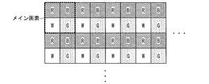
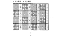
- FIG. 2 is a diagram showing an arrangement of sub-pixels constituting a main pixel provided in the display panel of the liquid crystal display device shown in FIG.
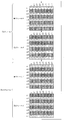
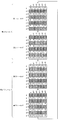
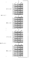
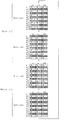
- FIG. 6 is a transition diagram schematically showing how the polarity of each sub-pixel changes when 1-dot inversion driving is performed while performing 1-line interlaced driving in the liquid crystal display device according to an embodiment of the present invention. is there. It is a timing chart which shows the relationship between a scanning signal and a data signal.
- FIG. 2 is a diagram showing an arrangement of sub-pixels constituting a main pixel provided in the display panel of the liquid crystal display device shown in FIG.
- FIG. 6 is a transition diagram schematically showing how the polarity of each sub-pixel changes when 1-dot inversion driving is performed while performing 1-line interlaced driving in the liquid crystal display device according to an embodiment of the present invention. is there. It is a timing chart which
- FIG. 6 is a transition diagram schematically showing how the polarity of each sub-pixel changes when 1-dot inversion driving is performed while performing 1-line interlaced driving in the liquid crystal display device according to an embodiment of the present invention. is there.
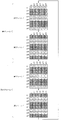
- FIG. 6 is a transition diagram schematically showing how the polarity of each sub-pixel changes when 2-dot inversion driving is performed while performing 1-line interlaced driving in the liquid crystal display device according to an embodiment of the present invention. is there.
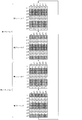
- FIG. 6 is a transition diagram schematically showing how the polarity of each sub-pixel changes when 2-dot inversion driving is performed while performing 2-line interlaced driving in the liquid crystal display device according to an embodiment of the present invention. is there.
- FIG. 6 is a transition diagram schematically showing how the polarity of each sub-pixel changes when 2-dot inversion driving is performed while performing 2-line interlaced driving in the liquid crystal display device according to an embodiment of the present invention. is there.
- FIG. 6 is a transition diagram schematically showing how the polarity of each sub-pixel changes when performing one-dot inversion driving while performing one-line interlaced driving in a liquid crystal display device according to another embodiment of the present invention. It is.
- FIG. 7 is a transition diagram schematically showing how the polarity of each sub-pixel changes when performing 2-dot inversion driving while performing 1-line interlaced driving in a liquid crystal display device according to another embodiment of the present invention. It is.
- FIG. 7 is a transition diagram schematically showing how the polarity of each sub-pixel changes when performing one-dot inversion driving while performing two-line interlaced driving in a liquid crystal display device according to another embodiment of the present invention. It is.
- FIG. 7 is a transition diagram schematically showing how the polarity of each sub-pixel changes when performing 2-dot inversion driving while performing 2-line interlaced driving in a liquid crystal display device according to another embodiment of the present invention. It is. FIG. 7 is a transition diagram schematically showing how the polarity of each sub-pixel changes when performing 2-dot inversion driving while performing 2-line interlaced driving in a liquid crystal display device according to another embodiment of the present invention. It is. It is a figure which is provided in the display panel of the liquid crystal display device which concerns on further another embodiment of this invention, and shows arrangement
- liquid crystal display device when the 1-line interlace drive and the 1-dot inversion drive are performed, how the polarity of each sub-pixel changes is schematically illustrated. It is a transition diagram. In the liquid crystal display device according to yet another embodiment of the present invention, how the polarity of each sub-pixel changes when performing 1-line interlaced driving and 2-dot inversion driving is schematically shown. It is a transition diagram. In a liquid crystal display device according to still another embodiment of the present invention, how the polarity of each sub-pixel changes when performing two-line interlaced driving and one-dot inversion driving is schematically shown. It is a transition diagram.
- liquid crystal display device In the liquid crystal display device according to still another embodiment of the present invention, how the polarity of each sub-pixel changes when performing 2-line interlace driving and 2-dot inversion driving is schematically shown. It is a transition diagram. In the liquid crystal display device according to still another embodiment of the present invention, how the polarity of each sub-pixel changes when performing 2-line interlace driving and 2-dot inversion driving is schematically shown. It is a transition diagram. It is a figure which is provided in the display panel of the liquid crystal display device which concerns on further another embodiment of this surface, and shows arrangement
- a liquid crystal display device In a liquid crystal display device according to still another embodiment of the present invention, how the polarity of each sub-pixel changes when performing three-line interlaced driving and one-dot inversion driving is schematically shown. It is a transition diagram. In the liquid crystal display device according to still another embodiment of the present invention, how the polarity of each sub-pixel changes when performing 3-line interlace driving and 3-dot inversion driving is schematically shown. It is a transition diagram. In the flat display device disclosed in Patent Literature 1, scanning is performed by thinning out scanning lines for each line, and a timing chart in a case where one image is formed by two frames is shown. FIG. 6 is a transition diagram schematically showing how the polarity of each sub-pixel changes when performing m-dot inversion driving while performing one-line interlaced driving in the liquid crystal display device according to an embodiment of the present invention. is there.
- the display device is a liquid crystal display device including a display panel which is a liquid crystal display (LCD)
- LCD liquid crystal display
- the present invention is not limited to this. is not.
- the display device according to the present invention may be, for example, a PDP display device including a plasma display (PD), or an EL display device including an EL (Electro Luminescence) display.
- FIG. 1 is a diagram illustrating an overall configuration of a liquid crystal display device 1 according to Embodiment 1.
- FIG. 1 is a diagram illustrating an overall configuration of a liquid crystal display device 1 according to Embodiment 1.
- a liquid crystal display device 1 includes a display panel (liquid crystal display panel) 2, a timing controller 4 (control means), a scanning line driving circuit 6 (gate line driving circuit), and a signal line driving circuit 8 (data line). Drive circuit), a common electrode drive circuit 10, and a power supply generation circuit 13.
- the display panel 2 has a total of P rows (where P is an integer equal to or greater than 1) scanning lines (gate lines), and a total number of Q columns (Q is an integer equal to or greater than 1) arranged so as to intersect the scan lines. ) Data signal lines (data lines) and a plurality of sub-pixels arranged corresponding to the intersections of the scanning lines and the data signal lines. As will be described later, a predetermined number of sub-pixels constitute a main pixel (picture element) as one group.
- the timing controller 4 uses the gate output control signal GOE to control the timing at which the scanning line driving circuit 6 scans (selects) the scanning line.
- the timing controller 4 controls the polarity of the data signal supplied from the signal line drive circuit 8 using the polarity inversion signal.
- the timing controller 4 supplies a scanning signal (gate signal) to a scanning line (selected scanning line) selected in a certain field, and then selects a scanning line selected next to the selected scanning line.
- the signal line drive current (data line drive current) I2 supplied to an arbitrary data line during the period until the scan signal is supplied is transferred to the arbitrary data line when the scan signal is supplied to the selected scan line.
- the signal line drive circuit 8 is controlled so as to be reduced by a predetermined rate compared to the supplied signal line drive current I1.
- the arbitrary data line may be a part of the data line of the Q column or all of the data lines of the Q column.
- the signal line drive circuit 8 drives the signal line drive current I2 to decrease by a predetermined rate compared to the signal line drive current I1 in accordance with an instruction from the timing controller 4.
- the signal line driving circuit 8 sets the data signal line in a high impedance state, or reduces the signal line driving current capability of an output stage amplifier (so-called voltage follower) included in the signal line driving circuit 8.
- the drive current I2 may be reduced by a predetermined rate compared to the signal line drive current I1.
- the signal line driving current I2 may be driven so as to be reduced by about 30% compared to the signal line driving current I2.
- the signal line drive current I2 is about 70% of the signal line drive current I1.
- the signal line driving current I2 is reduced by 100% in the signal line driving circuit 8, thereby setting the signal line driving current I2 to 0 and setting the absolute value of the potential of the applied data signal to 0V.
- the signal line driving circuit 8 stops supplying the signal line driving current, that is, stops applying the data signal.
- the scanning line driving circuit 6 starts scanning the scanning line with the gate start pulse signal received from the timing controller 4 as a signal.
- the scanning line driving circuit 6 sequentially selects the selection voltage from the first scanning line of the display panel 2 for each scanning line in accordance with the gate clock signal GCK and the gate output control signal GOE received from the timing controller 4. Is applied.
- the scanning line driving circuit 6 sequentially supplies a scanning signal, which is a voltage for turning on a switching element (TFT) provided in each sub-pixel on the scanning line, to each scanning line. Accordingly, the scanning line driving circuit 6 sequentially selects and scans each scanning line. Note that supplying a scanning signal that is a voltage for turning on the switching element is hereinafter referred to as scanning a scanning line.
- the scanning line driving circuit 6 sequentially selects each scanning line according to the received gate clock GCK signal.
- the scanning line driving circuit 6 supplies the scanning line driving current (gate line driving current) to the selected scanning line at the timing when the falling edge of the received gate output control signal GOE is detected, thereby selecting the selected voltage. (That is, a scanning signal) is applied. Thereby, the scanning line driving circuit 6 scans the selected scanning line. Further, the scanning line driving circuit 6 can perform interlace driving, as will be described later.
- applying a scanning signal to a scanning line by supplying a scanning line driving current is also simply referred to as applying (or supplying) the scanning signal.
- the signal line driving circuit 8 stores the input image data of each sub-pixel in a register according to the source clock signal based on the source start pulse signal received from the timing controller 4. Further, the signal line driving circuit 8 supplies a data signal, which is image data, to each data signal line of the display panel 2 in accordance with the next source latch strobe signal, and a pixel electrode provided in a sub-pixel including each data signal line. To charge.
- the signal line drive circuit 8 calculates the value of the voltage to be output to each sub-pixel on the selected scanning line based on the input video signal (arrow A), and the voltage ( That is, a data signal is output to each data signal line by supplying a signal line drive current. As a result, image data is supplied to each sub-pixel on the selected scanning line.
- applying a data signal to a data signal line by supplying a signal line driving current is simply expressed as applying (or supplying) the data signal.
- the signal line driving circuit 8 sets the polarity of the data signal applied to the selected pixel that is a sub-pixel to be selected in a certain field in accordance with the polarity inversion signal received from the timing controller 4 in the row direction and the column direction, respectively.
- the number of selected pixels is inverted as a unit, and the polarity of the data signal applied to each selected pixel in a certain field is set to the data applied to the selected pixel in the field immediately before the certain field. Invert with respect to signal polarity.
- the power generation circuit 13 generates a voltage necessary for each circuit in the liquid crystal display device 1 to operate. Then, the power supply generation circuit 13 outputs the generated voltage to the scanning line driving circuit 6, the signal line driving circuit 8, the timing controller 4, and the common electrode driving circuit 10.
- the liquid crystal display device 1 includes a common electrode (not shown) provided for each sub-pixel in the display panel 2.
- the common electrode drive circuit 10 outputs a predetermined common voltage for driving the common electrode to the common electrode based on a signal (arrow B) input from the timing controller 4 (arrow C).
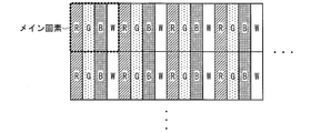
- FIG. 2 is a diagram illustrating an arrangement of sub-pixels constituting the main pixel provided in the display panel 2 of the liquid crystal display device 1 according to the present embodiment.
- three sub-pixels that individually display the three primary colors (sub-pixel R that displays red, sub-pixel B that displays blue, and sub-pixel G that displays green), and three primary colors
- One main pixel (picture element) is configured with four sub-pixels of sub-pixels (sub-pixels W displaying white) that display one color obtained by combining at least one of them as a unit. Further, these four sub-pixels are arranged so as to be arranged two by two in the column direction and the row direction, respectively. For example, as shown in FIG.
- sub-pixel R and sub-pixel B, sub-pixel W and sub-pixel G is adjacent to each other in the row direction, and the sub pixel R and the sub pixel W, and the sub pixel B and the sub pixel G are adjacent to each other in the column direction.
- the sub-pixel R and the sub-pixel B, the sub-pixel W and the sub-pixel G are adjacent in the row direction, and the sub-pixel R and the sub-pixel W, the sub-pixel B and the sub-pixel G are in the column direction.
- the arrangement method of the four sub-pixels is 4 factorials, that is, 24 methods.
- the sub-pixel R and the sub-pixel G, the sub-pixel W and the sub-pixel B are adjacent to each other in the row direction.
- the pixel R, the sub-pixel W, the sub-pixel G, and the sub-pixel B may be arranged so as to be adjacent in the column direction.
- a case where four subpixels of a subpixel W that displays white are used as one color obtained by combining at least one of the three primary colors will be described as an example. It is not limited to this.
- the sub pixel W that displays white the sub pixel Y that displays yellow may be used, or only one of the three primary colors (either red, blue, or green) may be used.
- a configuration using sub-pixels for displaying other colors may be adopted.
- Interlaced drive When performing interlaced driving, one frame is divided into units called fields (a scanning line scanned in one frame is divided into a plurality of sets scanned in each field), and scanning is performed sequentially for each field. Go.
- the scanning line drive circuit 6 thins out the scanning lines for supplying scanning signals for each scanning line in a certain field (hereinafter also referred to as a first field). Scan by skipping one line.
- the scanning lines not scanned in the first field are scanned. That is, when the first field is configured by scanning odd-numbered scanning lines, the second field is configured by scanning even-numbered scanning lines.
- the present embodiment is not limited to the case where the first field and the second field are configured by scanning one scanning line, but scanning each field by scanning two scanning lines. You may comprise by.
- interlaced driving method in the i-th field, scanning is performed every j scanning lines in the order of kth, k + (j + 1) th, k + 2 (j + 1) th,.
- interlace driving is performed by scanning every j scanning lines in the order of k + 1, k + 1 + (j + 1) th, k + 1 + 2 (j + 1) th,... May be.
- the signal line driving circuit 8 selects the scanning line to be selected next to a certain scanning line from the time when the scanning line driving circuit 6 finishes selecting the scanning line in the first field of a certain frame. In the period until it is set, the data signal is driven to have a potential of 0V.
- the scanning line driving circuit 6 and the signal line driving circuit 8 operate in the second field of a certain frame in the same manner as the first field. Further, in the first field (or second field) of the next frame of a certain frame, the scanning line driving circuit 6 and the signal line driving circuit 8 operate in the same manner as the first field (or second field) of the certain frame. To do.
- the timing controller 4 when applying the scanning signal and the data signal using the interlace driving method, applies the scanning signal to the scanning line selected in a certain field, and then selects the selected one. Compare the signal line driving current in the period until the scanning signal is applied to the scanning line selected next to the scanning line to the signal line driving current when the scanning signal is applied to the selected scanning line. Then, the signal line driving circuit 8 is controlled so as to decrease by a predetermined rate.
- the signal is applied during the period from when the scanning signal is applied to the scanning line selected next to the selected scanning line.
- the power consumed to supply the line driving current can be reduced.
- the timing controller 4 applies the scanning signal to the scanning line selected after the selected scanning line after the scanning signal is applied to the scanning line selected in a certain field.
- the signal line driving circuit 8 is controlled so that the absolute value of the potential of the scanning signal is set to 0V by setting the supply of the signal line driving current to 0 in the period until the voltage is applied.
- the signal is applied during the period from when the scanning signal is applied to the scanning line selected next to the selected scanning line.
- the power consumed to supply the line drive current can be further reduced.
- the operation of the signal line driving circuit 8 described above may be used together with inversion driving or may not be used together.
- the operation of the signal line driving circuit 8 when operating in combination with inversion driving will be described below.
- FIG. 3 is a transition diagram schematically showing how the polarity of each sub-pixel changes in the liquid crystal display device 1 of the present embodiment.
- the first field includes p (where 1 ⁇ p ⁇ P-11) row scanning line, p + 2 row scanning line, p + 4 The scanning line in the row and the scanning line in the p + 6th row are scanned.
- the second field is configured by scanning the p + 1th scanning line, the p + 3th scanning line, the p + 5th scanning line, and the p + 7th scanning line. That is, the first field and the second field are configured by scanning one scan line at a time.
- the scanning line driving circuit 6 scans the pth scanning line, the p + 2th scanning line, the p + 4th scanning line, and the p + 6th row.
- the scanning lines are sequentially scanned.
- the scanning of the p + 1-th scanning line, the p + 3-th scanning line, the p + 5-th scanning line, and the p + 7-th scanning line, which are the scanning lines of the second field, is thinned out.
- the scanning line driving circuit 6 scans the scanning lines for each scanning line from the first scanning line to the Pth scanning line.
- the signal line driving circuit 8 performs q (where 1 ⁇ q ⁇ Q-15) A data signal having a polarity “+” is supplied to the data signal line in the column, and a data signal having a polarity “+” is supplied to the data signal line in the q + 1 column.
- the signal line driving circuit 8 supplies a data signal having a polarity of “ ⁇ ” to the data signal lines in the q + 2 column and the q + 3 column, and the data signals in the q + 4 column and the q + 5 column
- a data signal having a polarity “+” is supplied to the line
- a data signal having a polarity “ ⁇ ” is supplied to the data signal lines in the q + 6th column and the q + 7th column.
- the signal line driving circuit 8 thus operates when the scanning line driving circuit 6 scans the p-th scanning line to the Q-th data signal line. Until then, the data signal having the same polarity is supplied to each of the two sub-pixels arranged in the row direction constituting the main pixel indicated by the broken line in FIG. In other words, with respect to the row direction, the polarity of the data signal applied to each sub pixel is inverted with two sub pixels arranged in the row direction constituting the main pixel as one unit.
- the signal line driving circuit 8 has a polarity “ The data signal having “ ⁇ ” is supplied, and the data signal having the polarity “ ⁇ ” is supplied to the data signal line in the q + 1th column. Further, the signal line drive circuit 8 supplies a data signal having a polarity of “+” to the data signal lines in the q + 2 column and the q + 3 column, and the data signals in the q + 4 column and the q + 5 column. A data signal having a polarity of “ ⁇ ” is supplied to the line, and a data signal having a polarity of “+” is supplied to the data signal lines in the q + 6th column and the q + 7th column.
- the signal line driving circuit 8 shifts the main pixel from the first column data signal line to the Q column data signal line. Driving is performed so that data signals having the same polarity are supplied to every two sub-pixels arranged in the row direction.
- subpixels (hereinafter referred to as (p, q) -th) defined by the scanning line in the p-th row and the data signal line in the q-th column.
- the polarity of the data signal applied to R) (also referred to as a sub-pixel) is “+” as shown in FIG.
- the polarity of the data signal applied to the (p + 2, q) -th subpixel R and the (p, q + 2) -th subpixel R is “ ⁇ ” as shown in FIG.
- the polarity of the data signal applied to the (p, q + 1) th sub-pixel B is “+” as shown in FIG.
- the polarity of the data signal applied to the (p + 2, q + 1) th sub-pixel B and the (p, q + 3) -th sub-pixel B is “ ⁇ ” as shown in FIG.
- the signal line driving circuit 8 is a sub-pixel that displays the same color among the sub-pixels defined by the scanning lines scanned in the first field and is closest to each other.
- data signals having opposite polarities are applied.
- the signal line driving circuit 8 has two units of main pixels in the row direction and one sub-pixel in the column direction in one unit (that is, 2 ⁇ 1) in the row direction and the column direction, respectively.
- the polarity of the data signal applied to each selected pixel is inverted using the selected pixel group as one unit.
- the scanning line driving circuit 6 includes, in the second field of the x-th frame, the p + 1th scanning line, the p + 3th scanning line, the p + 5th scanning line, and the p + 7th.
- the scanning lines in the row are sequentially scanned.
- the scanning of the p-th scanning line, the p + 2th scanning line, the p + 4th scanning line, and the p + 6th scanning line as the first field is thinned out. In this way, scanning is performed with one scanning line skipped from the first scanning line to the Pth scanning line. Therefore, as shown in FIG. 3, the scanning line driving circuit 6 performs one-line interlaced driving by repeating scanning of the first field scanning line and scanning of the second field scanning line.
- the signal line driving circuit 8 applies the data signal line of the q-th column.
- a data signal having a polarity “+” is supplied, and a data signal having a polarity “+” is supplied to the data signal line in the q + 1th column.
- the signal line driving circuit 8 supplies a data signal having a polarity of “ ⁇ ” to the data signal lines in the q + 2 column and the q + 3 column, and the data signals in the q + 4 column and the q + 5 column
- a data signal having a polarity “+” is supplied to the line
- a data signal having a polarity “ ⁇ ” is supplied to the data signal lines in the q + 6th column and the q + 7th column.
- the signal line driving circuit 8 when the scanning line driving circuit 6 scans the p + 3th scanning line, the signal line driving circuit 8 has a polarity “ The data signal having “ ⁇ ” is supplied, and the data signal having the polarity “ ⁇ ” is supplied to the data signal line in the q + 1th column. Further, the signal line drive circuit 8 supplies a data signal having a polarity of “+” to the data signal lines in the q + 2 column and the q + 3 column, and the data signals in the q + 4 column and the q + 5 column. A data signal having a polarity of “ ⁇ ” is supplied to the line, and a data signal having a polarity of “+” is supplied to the data signal lines in the q + 6th column and the q + 7th column.
- the signal line driving circuit 8 thus operates when the scanning line driving circuit 6 scans the p-th scanning line to the Q-th data signal line. Up to this time, driving is performed so as to supply data signals having the same polarity for every two sub-pixels arranged in the row direction.
- the polarity of the data signal applied to the (p + 1, q) th sub-pixel W is “+” as shown in FIG. It becomes the polarity. Further, the polarity of the data signal applied to the (p + 3, q) th sub-pixel W and the (p + 1, q + 2) -th subpixel W is “ ⁇ ” as shown in FIG.
- the polarity of the data signal applied to the (p + 1, q + 1) th sub-pixel G is “+” as shown in FIG.
- the polarity of the data signal applied to the (p + 3, q + 1) th sub-pixel B and the (p + 1, q + 3) -th subpixel B is “ ⁇ ” as shown in FIG.
- the signal line driving circuit 8 is a sub-pixel displaying the same color among the sub-pixels defined by the scanning lines scanned in the second field, and the polarities of the sub-pixels closest to each other are mutually different. Apply the opposite data signal.
- the polarity of the data signal applied to each selected pixel selected in a certain field is the polarity of the data signal applied to the selected pixel in the field immediately before the certain field. Is reversed with respect to.
- the scanning line driving circuit 6 repeats scanning and non-scanning for each field with respect to each scanning line, and the signal line driving circuit 8 performs data signal supply to each data signal line for each frame. Drive to reverse polarity.
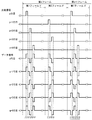
- FIG. 4 is a timing chart showing the relationship between the scanning signal and the data signal.
- a scanning signal having a high level (H level) voltage is applied to the p-th scanning line at time T1 (that is, the p-th scanning line).
- supply of data signals having a polarity of “+” is started to the data signal lines in the q-th, q + 1-th and q + 4-th columns, as shown in FIG. .
- supply of a data signal having a polarity of “ ⁇ ” is started to the data signal lines in the q + 2 and q + 3 columns.
- the potential of the data signal supplied to each data signal line becomes 0 V substantially simultaneously with the selection of the scanning line in the p-th row at time T2. That is, at time T2, the supply of the data signal to each data signal line is stopped. The stop of the supply of the data signal is maintained until the p + 2th scanning line is selected at time T3.
- the supply of a data signal having a polarity opposite to the polarity of is started.
- the potential of the data signal supplied to each data signal line becomes 0 V substantially at the same time when selection of the p-th scanning line is completed at time T12.
- a data signal having a polarity opposite to the polarity of the data signal supplied in the first field of the xth frame is applied to each data signal line.
- Supply is started.
- the potential of the data signal supplied to each data signal line becomes 0 V substantially at the same time when the scanning of the scanning line of the (p + 2) th row is completed at time T14.
- the timing controller 4 inverts the polarity of the data signal for each predetermined number of selected pixels and sets the polarity of the data signal applied to each selected pixel in a certain field to the field in which the selected pixel is selected.
- the signal line driving circuit 8 is controlled so as to invert the polarity of the data signal applied to the selected pixel in the field immediately before the certain field. As a result, the scanning line driving circuit 6 and the signal line driving circuit 8 are driven to apply the dot inversion driving to the gate line selected by the interlace driving.
- the timing controller 4 changes the polarity of the data signal applied to each selected pixel in the first field (or second field) of the xth frame to the first field (or the first field of the x + 1th frame).
- the signal line driver circuit is controlled so as to invert in (2 fields).
- the scanning line driving circuit 6 and the signal line driving circuit 8 perform 1-line interlaced driving and 1-dot inversion driving, they are arranged in the row direction constituting the main pixel in the row direction.
- the signal line driving circuit 8 is a sub-pixel that configures each main pixel adjacent to each other by applying data signals of different polarities to two sub-pixels arranged in the row direction constituting the main pixel in the row direction.
- a configuration may be adopted in which the polarity of the data signal applied to each subpixel is inverted with two subpixels adjacent in the row direction as one unit.
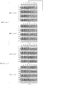
- FIG. 5 is a transition diagram schematically showing how the polarity of each sub-pixel changes in the liquid crystal display device 1 according to the present embodiment.
- the scanning line driving circuit 6 scans the p-th scanning line, the p + 2th scanning line, the p + 4th scanning line, and the p + 6th row.
- the scanning lines are sequentially scanned.
- the scanning of the p + 1-th scanning line, the p + 3-th scanning line, the p + 5-th scanning line, and the p + 7-th scanning line, which are the scanning lines of the second field, is thinned out.
- the scanning line driving circuit 6 scans scanning lines from the first scanning line to the P-th scanning line by skipping one line, and switches between scanning and non-scanning for each field. .
- the signal line driving circuit 8 is a sub-pixel constituting another main pixel, and applies a data signal having the same polarity to two sub-pixels adjacent in the row direction.
- the polarity of the data signal applied to each sub-pixel arranged adjacent to each other in the column direction among the sub-pixels defined by the scanning lines scanned in each field is inverted.
- the data signals applied to the (p, q + 1) th subpixel B and the (p, q + 2) th subpixel R are changed.
- the polarity is “+” as shown in FIG.
- the (p + 2, q + 1) th subpixel B, the (p, q + 3) th subpixel B, the (p + 2, q + 2) th subpixel R, and the (p, q + 4) th subpixel R are applied.
- the polarity of the data signal is “ ⁇ ” as shown in FIG.
- the polarity of the data signal applied to each selected pixel selected in a certain field is the polarity of the data signal applied to the selected pixel in the field immediately before the certain field. Is reversed with respect to.
- the scanning line driving circuit 6 repeats scanning and non-scanning for each field with respect to each scanning line, and the signal line driving circuit 8 performs data signal supply to each data signal line for each frame. Drive to reverse polarity.
- the supply of the data signal having the polarity shown in FIG. 5 is started to each data signal line almost simultaneously with the selection of the (p + 1) th scanning line (time t2).
- the potential of the supplied data signal becomes 0 V almost simultaneously with the selection of the scanning line of the (p + 1) th row, and is maintained until the scanning line of the (p + 3) th row is selected.
- the first field (or second field) of the (x + 1) th frame is applied to each data signal line substantially simultaneously with the selection of each scanning line.
- the supply of the data signal having the opposite polarity to the polarity of the data signal supplied in (1) is sequentially started.
- the potential of the data signal supplied to each data signal line becomes 0 V substantially simultaneously when the scanning of each scanning line is completed.
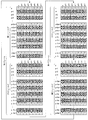
- FIG. 6 schematically shows how the polarity of each sub-pixel changes in the liquid crystal display device 1 according to the present embodiment when 1-line interlace driving is performed and 2-dot inversion driving is performed. It is a transition diagram.
- the scanning line driving circuit 6 scans the p-th scanning line, the p + 2th scanning line, the p + 4th scanning line, and the p + 6th row.
- the scanning lines are sequentially scanned.
- the scanning line driving circuit 6 scans the p + 1-th scanning line, the p + 3-th scanning line, the p + 5-th scanning line, and the p + 7-th scanning line that are the scanning lines of the second field. Is thinned out.
- the scanning line driving circuit 6 scans the scanning lines from the first scanning line to the P-th scanning line, skipping one line, and switching between scanning and non-scanning for each field. .
- the signal line driving circuit 8 applies a data signal having the same polarity to each of the two sub-pixels arranged in the row direction constituting the main pixel.
- the polarity of the data signal applied to each sub-pixel arranged adjacent to each other in the column direction among the sub-pixels defined by the scanning lines scanned in each field is inverted.
- the signal line driving circuit 8 performs the row direction that constitutes the main pixel from the first data signal line to the Qth data signal line. Are driven so as to supply data signals of the same polarity to the two sub-pixels arranged in a row.
- the data signals applied to the (p, q) th subpixel R and the (p + 2, q) th subpixel R The polarity is “+” as shown in FIG. Further, it is applied to the (p + 4, q) th subpixel R, the (p + 6, q) th subpixel R, the (p, q + 2) th subpixel R, and the (p + 2, q + 2) th subpixel R.
- the polarity of the data signal is “ ⁇ ” as shown in FIG.
- the polarities of the data signals applied to the (p + 1, q) th subpixel W and the (p + 3, q) th subpixel W in the second field of the xth frame are shown in FIG.
- the polarity is “+”.
- the (p + 5, q) th subpixel W, the (p + 7, q) th subpixel W, the (p + 1, q + 2) th subpixel W, and the (p + 3, q + 2) th subpixel W are applied.
- the polarity of the data signal is “ ⁇ ” as shown in FIG.
- the signal line driving circuit 8 is a sub-pixel that displays the same color among the sub-pixels defined by the scanning lines scanned in the first field or the second field of the x-th frame.
- the data signal is supplied so that the polarity is inverted every two sub-pixels closest to each other in the column direction and the polarity of each sub-pixel closest to the row direction is inverted, thereby performing 2-dot inversion driving.
- the signal line driving circuit 8 includes two sub-pixels constituting the main pixel in the row direction and two sub-pixels in the column direction in one unit (that is, in the row direction and the column direction).
- the polarity of the data signal applied to each selected pixel is inverted using a 2 ⁇ 2 selected pixel group as one unit.
- the polarity of the data signal applied to each selected pixel selected in a certain field is the polarity of the data signal applied to the selected pixel in the field immediately before the certain field. Is reversed with respect to.
- the supply of the data signal having the polarity shown in FIG. 6 is started to each data signal line substantially simultaneously with the selection of the p-th scanning line (time t3).
- the potential of the supplied data signal becomes 0 V substantially simultaneously with the end of scanning of the p-th scanning line, and is maintained until the p + 2th scanning line is selected.
- the supply of the data signal having the polarity shown in FIG. 6 is started to each data signal line substantially simultaneously with the selection of the (p + 1) th scanning line (time t4).
- the potential of the data signal supplied to each data signal line becomes 0 V substantially at the same time as the selection of the p + 1-th scanning line is completed, and is maintained until the p + 3-th scanning line is selected.
- the first field (or second field) of the (x + 1) th frame is applied to each data signal line substantially simultaneously with the selection of each scanning line.
- the supply of the data signal having the opposite polarity to the polarity of the data signal supplied in (1) is sequentially started.
- the potential of the data signal supplied to each data signal line becomes 0 V almost simultaneously with the selection of each scanning line.
- FIG. 7 schematically shows how the polarity of each sub-pixel changes in the liquid crystal display device 1 according to the present embodiment when 2-line interlace driving is performed and 2-dot inversion driving is performed. It is a transition diagram.
- the first field includes p-th scanning line, p + 3-th scanning line, p + 4-th scanning line, and p + 7-th scanning line as shown in FIG. It shall be constituted by scanning.
- the second field is configured by scanning the p + 1-th scanning line, the p + 2-th scanning line, the p + 5-th scanning line, and the p + 6-th scanning line.
- the first field and the second field are configured by scanning with two scanning lines skipped.
- the scanning line driving circuit 6 scans the p-th scanning line, the p + 3th scanning line, the p + 4th scanning line, and the p + 7th row.
- the scanning lines are sequentially scanned.
- the scanning of the p + 1-th scanning line, the p + 2-th scanning line, the p + 5-th scanning line, and the p + 6-th scanning line as the second field is thinned out.
- the scanning line driving circuit 6 scans the scanning lines by skipping two rows from the first scanning line to the Pth scanning line, and switches between scanning and non-scanning for each field. .
- the signal line driving circuit 8 applies a data signal having the same polarity to each of the two sub-pixels arranged in the row direction constituting the main pixel. Further, the polarity of the data signal applied to each of the two subpixels arranged closest to each other in the column direction among the subpixels defined by the scanning lines scanned in each field is inverted.
- the signal line driving circuit 8 performs the row direction that constitutes the main pixel from the first data signal line to the Qth data signal line. Are driven so as to apply data signals of the same polarity to the two sub-pixels arranged in a row.
- the scanning line driving circuit 6 and the signal line driving circuit 8 perform the above-described driving, so that the data signal applied to the (p, q) th subpixel R and the (p + 3, q) th subpixel W.
- the polarity is “+” as shown in FIG.
- it is applied to the (p + 4, q) th subpixel R, the (p, q + 2) th subpixel R, the (p + 7, q) th subpixel W, and the (p + 3, q + 2) th subpixel W.
- the polarity of the data signal is “ ⁇ ” as shown in FIG.
- the polarities of the data signals applied to the (p + 1, q) th subpixel W and the (p + 2, q) th subpixel R in the second field of the xth frame are shown in FIG.
- the polarity is “+”.
- it is applied to the (p + 5, q) th subpixel W, the (p + 6, q) th subpixel R, the (p + 1, q + 2) th subpixel W, and the (p + 2, q + 2) th subpixel R.
- the polarity of the data signal is “ ⁇ ” as shown in FIG.
- the signal line driving circuit 8 is a sub-pixel that displays the same color among the sub-pixels defined by the scanning lines scanned in the first field or the second field of the first frame.
- the one-dot inversion drive is performed so that the polarity of the data signal applied to the subpixels closest to each other in the row direction and the column direction is inverted.
- the signal line driving circuit 8 has two sub-pixels constituting the main pixel adjacent in the row direction and two sub-pixels adjacent in the column direction as one unit in the row direction and the column direction, respectively.
- the polarity of the data signal applied to each selected pixel is inverted as a unit of 2 ⁇ 2 selected pixel groups.
- the polarity of the data signal applied to each selected pixel selected in a certain field is the polarity of the data signal applied to the selected pixel in the field immediately before the certain field. Is reversed with respect to.
- the supply of the data signal having the polarity shown in FIG. 7 is started to each data signal line substantially simultaneously with the selection of the (p + 1) th scanning line (time t6).
- the potential of the data signal supplied to each data signal line becomes 0 V substantially at the same time as the selection of the p + 2 row scanning line after the p + 1 row scanning line is selected. Maintained until selected.
- the first field (or second field) of the (x + 1) th frame is applied to each data signal line substantially simultaneously with the selection of each scanning line.
- the supply of the data signal having the opposite polarity to the polarity of the data signal supplied in (1) is sequentially started. Then, the potential of the data signal supplied to each data signal line becomes 0 V substantially simultaneously when the selection of each scanning line is completed.
- the signal line driving circuit 8 sets two sub-pixels arranged in the row direction constituting the main pixel to 1 in the row direction.
- the signal line driving circuit 8 applies data signals having different polarities to two sub-pixels adjacent to each other in the row direction in the row direction, and the sub-pixels forming the main pixels adjacent to each other.
- a configuration may be adopted in which the polarity of the data signal applied to each sub pixel is inverted with two sub pixels adjacent in the row direction as one unit.
- FIG. 8 is a transition diagram schematically showing how the polarity of each sub-pixel changes in the liquid crystal display device 1 according to the present embodiment.
- the scanning line driving circuit 6 scans the pth scanning line, the p + 3th scanning line, the p + 4th scanning line, and the p + 7th row.
- the scanning lines are sequentially scanned.
- the scanning of the p + 1-th scanning line, the p + 2-th scanning line, the p + 5-th scanning line, and the p + 6-th scanning line as the second field is thinned out.
- the scanning line driving circuit 6 scans the scanning lines from the first scanning line to the P-th scanning line, skipping two lines, and switching between scanning and non-scanning for each field. .
- the signal line driving circuit 8 is a sub-pixel constituting another main pixel, and applies a data signal having the same polarity to two sub-pixels adjacent in the row direction.
- the polarity of the data signal applied to each subpixel arranged closest to the column direction among the subpixels defined by the scanning lines scanned in each field is inverted.
- the signal line driving circuit 8 configures other main pixels from the first column data signal line to the Qth column data signal line when the scanning line driving circuit 6 scans the scanning line.
- the sub-pixel is driven so as to supply data signals having the same polarity to two sub-pixels adjacent in the row direction.
- the scanning line driving circuit 6 and the signal line driving circuit 8 perform the above-described driving, so that the data signal applied to the (p, q) th subpixel R and the (p + 3, q) th subpixel W.
- the polarity is “ ⁇ ” as shown in FIG.
- it is applied to the (p + 4, q) th subpixel R, the (p, q + 2) th subpixel R, the (p + 7, q) th subpixel W, and the (p + 3, q + 2) th subpixel W.
- the polarity of the data signal is “+” as shown in FIG.
- the polarities of the data signals applied to the (p + 1, q) th subpixel W and the (p + 2, q) th subpixel R in the second field of the xth frame are shown in FIG.
- the polarity is “ ⁇ ”.
- it is applied to the (p + 5, q) th subpixel W, the (p + 6, q) th subpixel R, the (p + 1, q + 2) th subpixel W, and the (p + 2, q + 2) th subpixel R.
- the polarity of the data signal is “+” as shown in FIG.
- the signal line drive circuit 8 is a sub-pixel displaying the same color in the first field or the second field, and the data signals having opposite polarities to the sub-pixels closest to each other. Supply.
- the signal line driving circuit 8 is adjacent to each other in the row direction and the column direction.
- the polarity of the data signal applied to each selected pixel is inverted using two subpixels as one unit.
- the polarity of the data signal applied to each selected pixel selected in a certain field is the polarity of the data signal applied to the selected pixel in the field immediately before the certain field. Is reversed with respect to.
- the signal line driving circuit 8 when performing 2-line interlaced driving and 2-dot inversion driving, is adjacent to the adjacent two lines in which scanning is thinned out in the first field of each frame in the column direction.
- the signal line driving circuit 8 has two adjacent sub-pixels defined by the scanning lines sandwiched between the two scanning lines thinned out in the first field of each frame in the column direction as one unit.
- a configuration in which the polarity of the data signal applied to each sub-pixel is inverted may be employed.
- FIG. 9 shows a case where the liquid crystal display device 1 according to the present embodiment is sandwiched between two scanning lines that are thinned out in the first field of each frame when performing two-line interlaced driving and two-dot inversion driving.
- the scanning line driving circuit 6 performs p-line scanning line, p + 3 scanning line, p + 4th scanning line in the first field of the x-th frame in order to perform 2-line interlace driving.
- the scanning line and the scanning line of the p + 7th row are sequentially scanned.
- the scanning of the p + 2th scanning line, the p + 3th scanning line, the p + 5th scanning line, and the p + 6th scanning line, which are the scanning lines of the second field, is thinned out.
- the scanning line driving circuit 6 thus scans the scanning lines every two scanning lines from the first scanning line to the Pth scanning line. That is, the scanning line driving circuit 6 repeats scanning and non-scanning for each scanning line for every two scanning lines, and switches between scanning and non-scanning for each field.
- the signal line driving circuit 8 applies a data signal with reversed polarity to each of two sub-pixels arranged adjacent to each other in the row direction and constituting the main pixel, and is adjacent to the main line adjacent to the row direction.
- the polarity of the data signal applied for each pixel is inverted.
- the polarity of the data signal to be applied is inverted for every two adjacent sub-pixels defined by the scanning lines sandwiched between two scanning lines to be thinned out in the first field.
- the signal line drive circuit 8 applies a data signal with the polarity reversed every frame to the same subpixel.
- the signal line drive circuit 8 allows the sub-pixels constituting the main pixel from the data signal line in the first column to the data signal line in the Q column when the scan line drive circuit 6 scans the scan line.
- the driving is performed so that data signals having the same polarity are applied to two sub-pixels adjacent in the row direction.
- the polarity of the data signal applied to each subpixel is applied to each corresponding subpixel in the first field of the xth frame.
- the opposite of the polarity of the data signal is opposite to the polarity of the data signal applied to each corresponding subpixel in the second field of the xth frame.
- the polarity of the data signal applied to each selected pixel selected in a certain field is the polarity of the data signal applied to the selected pixel in the field immediately before the certain field. Is reversed with respect to.
- FIG. 30 schematically shows how the polarity of each sub-pixel changes in the liquid crystal display device 1 according to the present embodiment when 1-line interlace driving is performed and m-dot inversion driving is performed. It is a transition diagram.
- m dots indicate “m rows ⁇ 2 columns” selected pixels among the scanning pixels corresponding to the selected scanning line in each field, but this does not limit the present embodiment.
- the first field and the second field in each frame are configured by scanning the scanning lines by skipping one line as shown in FIG.
- the scanning line driving circuit 6 scans each scanning line in the p, p + 2,..., P + 2m ⁇ 2, p + 2m,. Are sequentially scanned. In this way, the scanning line driving circuit 6 scans the scanning lines from the first scanning line to the P-th scanning line, skipping one line, and switching between scanning and non-scanning for each field. .
- the signal line driving circuit 8 applies a data signal having the same polarity to each of the two sub-pixels arranged in the row direction constituting the main pixel. Further, the polarity of the data signal applied to each of the two subpixels arranged closest to each other in the column direction among the subpixels defined by the scanning lines scanned in each field is inverted.
- the polarity of the data signal applied to the (p + 2m + 1, q) th,..., (P + 4m ⁇ 1, q) th subpixel W is “+”.
- the polarity of the signal is “-”.
- the polarity of the data signal applied to each subpixel is the same as that of the data signal applied to each corresponding subpixel in the first field of the xth frame. The opposite of polarity. Further, the polarity of the data signal applied to each sub-pixel in the second field of the (x + 1) th frame is opposite to the polarity of the data signal applied to each corresponding sub-pixel in the second field of the x-th frame. .
- the polarity of the data signal applied to each selected pixel selected in a certain field is the polarity of the data signal applied to the selected pixel in the field immediately before the certain field. Is reversed with respect to.
- the signal line driving circuit 8 is a sub-pixel that displays the same color among the sub-pixels defined by the scanning lines scanned in each field, and is m sub-pixels closest to each other in the column direction.
- the data signal is supplied so that the polarity is inverted for each pixel and the polarity is inverted for each sub-pixel closest to the row direction.
- the signal line driving circuit 8 is a sub-pixel displaying the same color among the sub-pixels constituting each picture element, and the polarity is inverted for each of the m sub-pixels closest to each other in the column direction, A data signal is supplied so that the polarity is inverted for each sub-pixel closest to the row direction.
- a liquid crystal display device according to another embodiment of the present invention will be described with reference to FIGS.
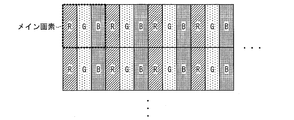
- FIG. 10 is a diagram showing an arrangement of four sub-pixels included in the display panel 2 of the liquid crystal display device 1 according to the present embodiment and constituting the main pixel.
- one main pixel is composed of four sub-pixels: a sub-pixel R, a sub-pixel B, a sub-pixel G, and a sub-pixel W.
- the four subpixels are arranged in a line in the row direction.
- the subpixel R, the subpixel G, the subpixel B, and the subpixel W are arranged in this order. Are arranged adjacent to each other in the row direction.
- the sub pixel R, the sub pixel G, the sub pixel B, and the sub pixel W are arranged adjacent to each other in the row direction.
- the arrangement method of the four sub-pixels is 4 factorials, that is, 24 methods.
- the sub-pixel R, the sub-pixel B, the sub-pixel G, and the sub-pixel W are adjacent in the row direction in this order. May be arranged.
- one main pixel is composed of four sub-pixels of a sub-pixel R, a sub-pixel B, a sub-pixel G, and a sub-pixel W
- the present invention is not limited to this.
- a configuration using the sub-pixel Y may be adopted, and of course, a configuration using sub-pixels for other colors may be adopted.
- FIG. 11 is a transition diagram schematically showing how the polarity of each sub-pixel changes in the liquid crystal display device 1 according to the present embodiment.
- the first field includes p-th scanning line, p + 2th scanning line, p + 4th scanning line, and p + 6th scanning line. It shall be constituted by scanning.
- the second field is configured by scanning the p + 1th scanning line, the p + 3th scanning line, the p + 5th scanning line, and the p + 7th scanning line. That is, the first field and the second field are configured by scanning one scan line at a time.
- the scanning line driving circuit 6 scans the p-th scanning line, the p + 2th scanning line, the p + 4th scanning line, and the p + 6th row.
- the scanning lines are sequentially scanned.
- the scanning of the p + 1-th scanning line, the p + 3-th scanning line, the p + 5-th scanning line, and the p + 7-th scanning line, which are the scanning lines of the second field, is thinned out.
- the scanning line driving circuit 6 scans the scanning lines for each scanning line from the first scanning line to the Pth scanning line.
- the signal line driving circuit 8 reads the data in the q-th column and the q + 2-th row.
- a data signal having a polarity “+” is supplied to the signal line, and a data signal having a polarity “ ⁇ ” is supplied to the data signal lines in the q + 1th column and the q + 3th row.
- the signal line drive circuit 8 supplies a data signal having a polarity of “ ⁇ ” to the data signal lines in the q + 4th column and the q + 6th column, and the polarity to the data signal line in the q + 5th column and the q + 7th column.
- a data signal that is “+” is supplied. Further, the signal line driving circuit 8 supplies a data signal having a polarity “+” to the data signal lines in the q + 8th column, the q + 10th column, the q + 13th column, and the q + 15th column, and the q + 9th column, the q + 11th column. A data signal having a polarity of “ ⁇ ” is supplied to the data signal lines in the first, q + 12th and q + 14th columns.
- the signal line driving circuit 8 applies the data signal lines in the qth column and the q + 2th row.
- a data signal having a polarity of “ ⁇ ” is supplied, and a data signal having a polarity of “+” is supplied to the data signal lines in the q + 1th column and the q + 3th row.
- the signal line driving circuit 8 supplies a data signal having a polarity of “+” to the data signal lines of the q + 4th column and the q + 6th column, and the polarity to the data signal line of the q + 5th column and the q + 7th column. Supply a data signal that is "-".
- the signal line driving circuit 8 supplies a data signal having a polarity of “ ⁇ ” to the data signal lines in the q + 8th column, the q + 10th column, the q + 13th column, and the q + 15th column, and the q + 9th column, the q + 11th column.
- a data signal having a polarity of “+” is supplied to the data signal lines of the first, q + 12th and q + 14th columns.
- the signal line driving circuit 8 is thus arranged so that when the scanning line driving circuit 6 scans the (p + 2) th scanning line, four signal lines are arranged adjacent to each other in the row direction constituting the main pixel. A data signal having an inverted polarity is applied to each sub pixel. Further, the signal line driving circuit 8 inverts the polarity of the data signal to be applied for each main pixel adjacent in the row direction.
- the polarities of the data signals applied to the (p, q) th subpixel R and the (p, q + 2) th subpixel B are as follows. As shown in FIG. 11, the polarity is “+”. Data applied to the (p + 2, q) th subpixel R, the (p, q + 4) th subpixel R, the (p + 2, q + 2) th subpixel B, and the (p, q + 6) th subpixel B. The polarity of the signal is “ ⁇ ” as shown in FIG.
- the polarity of the data signal applied to the (p, q + 1) th sub-pixel G and the (p, q + 3) -th sub-pixel W is “ ⁇ ” as shown in FIG.
- the polarity of the signal is “+” as shown in FIG.
- the polarities of the data signals applied to the (p + 1, q) th subpixel R and the (p + 1, q + 2) th subpixel B are as shown in FIG. “+” Polarity.
- the polarity of the signal is “ ⁇ ” as shown in FIG.
- the polarity of the data signal applied to the (p + 1, q + 1) th sub-pixel G and the (p + 1, q + 3) -th subpixel W is “ ⁇ ” as shown in FIG.
- the polarity of the signal is “+” as shown in FIG.
- the signal line driving circuit 8 is a sub-pixel displaying the same color among the sub-pixels defined by the scanning lines scanned in the first field, and data applied to the sub-pixels closest to each other. Drive so that the polarity of the signal is reversed.
- the polarity of the data signal applied to each subpixel is equal to the polarity of the data signal applied to each corresponding subpixel in the first field of the xth frame. The opposite of polarity. Further, the polarity of the data signal applied to each sub-pixel in the second field of the (x + 1) th frame is opposite to the polarity of the data signal applied to each corresponding sub-pixel in the second field of the x-th frame. .
- the polarity of the data signal applied to each selected pixel selected in a certain field is the polarity of the data signal applied to the selected pixel in the field immediately before the certain field. Is reversed with respect to.
- the scanning line driving circuit 6 performs one-line interlace driving for each scanning line, which repeats scanning and non-scanning for each scanning line and switches between scanning and non-scanning for each field.
- the signal line driving circuit 8 applies a data signal whose polarity is inverted for each sub-pixel to the four sub-pixels arranged adjacent to each other in the row direction and constituting the main pixel, and further in the row direction.
- One-dot inversion driving is performed to invert the polarity of the data signal applied to each adjacent main pixel.
- the signal line driving circuit 8 includes four sub-pixels constituting the main pixel in the row direction and one sub-pixel in the column direction in one unit (that is, in the row direction and the column direction).
- the polarity of the data signal applied to each selected pixel is inverted using a 4 ⁇ 1 selected pixel group as one unit.
- the signal line driving circuit 8 inverts the polarity of the data signal for each sub-pixel constituting the main pixel and also inverts the polarity of the data signal applied to each corresponding sub-pixel in the adjacent main pixels.
- a configuration can be adopted in which data signals having the same polarity are not applied to sub-pixels displaying the same color in the row direction.
- the supply of the data signal having the polarity shown in FIG. 11 is started to each data signal line substantially simultaneously with the selection of the p-th scanning line (time t7).
- the potential of the data signal supplied to each data signal line becomes 0V substantially at the same time as the selection of the p-th scanning line is completed, and is maintained until the p + 2th scanning line is selected.
- the supply of the data signal having the polarity shown in FIG. 11 is started to each data signal line substantially simultaneously with the selection of the (p + 1) th scanning line (time t8).
- the potential of the data signal supplied to each data signal line becomes 0 V substantially at the same time as the selection of the p + 1-th scanning line is completed, and is maintained until the p + 3-th scanning line is selected.
- the first field (or second field) of the (x + 1) th frame is applied to each data signal line substantially simultaneously with the selection of each scanning line.
- the supply of the data signal having the opposite polarity to the polarity of the data signal supplied in (1) is sequentially started.
- the potential of the data signal supplied to each data signal line becomes 0 V almost simultaneously with the selection of each scanning line.
- FIG. 12 schematically shows how the polarity of each sub-pixel changes in the liquid crystal display device 1 according to the present embodiment when 1-line interlace driving is performed and 2-dot inversion driving is performed. It is a transition diagram.
- the scanning line driving circuit 6 scans the pth scanning line, the p + 2th scanning line, the p + 4th scanning line, and the p + 6th scanning line.
- the scanning lines are sequentially scanned.
- the scanning line driving circuit 6 scans the p + 1-th scanning line, the p + 3-th scanning line, the p + 5-th scanning line, and the p + 7-th scanning line that are the scanning lines of the second field. Is thinned out.
- the scanning line driving circuit 6 scans the scanning lines from the first scanning line to the P-th scanning line, skipping one line, and switching between scanning and non-scanning for each field. .
- the signal line driving circuit 8 has four sub-pixels arranged adjacent to each other in the row direction constituting the main pixel during the scanning line driving circuit 6 scanning the scanning lines. On the other hand, a data signal with reversed polarity is applied to each sub-pixel. Further, the signal line driving circuit 8 inverts the polarity of the data signal to be applied for each main pixel adjacent in the row direction.
- the polarities of the data signals applied to the (p + 1, q + 1) th and (p + 3, q + 1) th subpixels G and the (p + 1, q + 3) th and (p + 3, q + 3) th subpixels W are as follows. As shown in FIG. 12, the polarity is “ ⁇ ”.
- the signal line driving circuit 8 has four sub-pixels constituting the main pixel in the row direction and two sub-pixels in the column direction in one unit (that is, in the row direction and the column direction).
- the polarity of the data signal applied to each selected pixel is inverted using a 4 ⁇ 2 selected pixel group as one unit.
- the polarity of the data signal applied to each selected pixel selected in a certain field is the polarity of the data signal applied to the selected pixel in the field immediately before the certain field. Is reversed with respect to.
- the scanning line driving circuit 6 repeats scanning and non-scanning for each scanning line for each scanning line, and switches between scanning and non-scanning for each field.
- the signal line driving circuit 8 applies a data signal whose polarity is inverted for each sub-pixel to four sub-pixels arranged adjacent to each other in the row direction and constituting the main pixel, and is adjacent in the row direction. The polarity of the data signal applied to each main pixel is inverted.
- the signal line driving circuit 8 further inverts the polarity of the data signal to be applied for every two subpixels adjacent in the column direction.
- the signal line drive circuit 8 inverts the polarity of the data signal for each sub-pixel constituting the main pixel, and further inverts the polarity of the data signal for each main pixel to display the same color in the row direction. It is possible to prevent a data signal having the same polarity from being applied to the pixel.
- the supply of the data signal having the polarity shown in FIG. 12 is started to each data signal line substantially simultaneously with the selection of the p-th scanning line (time t9).
- the potential of the data signal supplied to each data signal line becomes 0 V substantially simultaneously with the end of the selection of the p-th scanning line, and is maintained until the p + 2th scanning line is selected.
- the supply of the data signal having the polarity shown in FIG. 12 is started to each data signal line substantially simultaneously with the selection of the (p + 1) th scanning line (time t10).
- the potential of the data signal supplied to each data signal line becomes 0 V substantially at the same time as the selection of the p + 1-th scanning line is completed, and is maintained until the p + 3-th scanning line is selected.
- the first field (or second field) of the (x + 1) th frame is applied to each data signal line substantially simultaneously with the selection of each scanning line.
- the supply of the data signal having the opposite polarity to the polarity of the data signal supplied in (1) is sequentially started.
- the potential of the data signal supplied to each data signal line becomes 0 V almost simultaneously with the selection of each scanning line.
- FIG. 13 schematically shows how the polarity of each sub-pixel changes in the liquid crystal display device 1 according to the present embodiment when 2-line interlace driving is performed and 1-dot inversion driving is performed. It is a transition diagram.
- the scanning line driving circuit 6 has a p-th scanning line, a p + 3-th scanning line, and a p + 4-th row in the first field of the x-th frame.
- the scanning line and the scanning line of the p + 7th row are sequentially scanned.
- the scanning of the p + 2th scanning line, the p + 3th scanning line, the p + 5th scanning line, and the p + 6th scanning line which are the scanning lines of the second field, is thinned out.
- the scanning line driving circuit 6 scans the scanning lines from the first scanning line to the P-th scanning line, skipping two lines, and switching between scanning and non-scanning for each field. .
- the signal line driving circuit 8 includes four sub-pixels arranged adjacent to each other in the row direction constituting the main pixel when the scanning line driving circuit 6 scans the scanning line. On the other hand, a data signal with reversed polarity is applied to each sub-pixel. Further, the signal line driving circuit 8 inverts the polarity of the data signal to be applied for each main pixel adjacent in the row direction.
- the polarity of the data signal applied to is a “+” polarity as shown in FIG.
- the polarity of the signal is “ ⁇ ” as shown in FIG.
- the polarity of the data signal applied to the (p, q + 1) th sub-pixel G and the (p, q + 3) -th sub-pixel W is “ ⁇ ” as shown in FIG.
- the polarity of the signal is “+” as shown in FIG.
- the polarities of the data signals applied to the (p + 1, q) th subpixel R and the (p + 1, q + 2) th subpixel B are as shown in FIG. “+” Polarity.
- the polarity of the signal is “ ⁇ ” as shown in FIG.
- the polarity of the data signal applied to the (p + 1, q + 1) th sub-pixel G and the (p + 1, q + 3) -th subpixel W is a “ ⁇ ” polarity as shown in FIG.
- the polarity of the signal is “+” as shown in FIG.
- the signal line driving circuit 8 includes four sub-pixels constituting the main pixel in the row direction and one sub-pixel in the column direction in one unit (that is, in the row direction and the column direction).
- the polarity of the data signal applied to each selected pixel is inverted using a 4 ⁇ 1 selected pixel group as one unit.
- the polarity of the data signal applied to each selected pixel selected in a certain field is the polarity of the data signal applied to the selected pixel in the field immediately before the certain field. Is reversed with respect to.
- the scanning line driving circuit 6 repeats scanning and non-scanning of the scanning lines by skipping two lines for each scanning line, and further switches between scanning and non-scanning of the scanning lines for each field.
- the signal line driving circuit 8 applies a data signal with the polarity reversed for each sub-pixel to four sub-pixels arranged adjacent to each other in the row direction and constituting the main pixel.
- the polarity of the data signal applied every time is inverted.
- the signal line driver circuit 8 inverts the polarity of the data signal to be applied for each subpixel adjacent in the column direction. Further, the signal line drive circuit 8 applies a data signal with the polarity reversed every frame to the same subpixel.
- the supply of the data signal having the polarity shown in FIG. 13 is started to each data signal line almost simultaneously with the selection of the p-th scanning line (time t11).
- the potential of the data signal supplied to each data signal line becomes 0 V substantially at the same time as the selection of the p-th scanning line is completed, and is maintained until the p + 3th scanning line is selected.
- the supply of the data signal having the polarity shown in FIG. 13 is started to each data signal line substantially simultaneously with the selection of the (p + 1) th scanning line (time t12). .
- the potential of the data signal supplied to each data signal line becomes 0 V substantially at the same time as the selection of the p + 2 row scanning line after the p + 1 row scanning line is selected. Maintained until selected.
- the first field (or second field) of the (x + 1) th frame is applied to each data signal line substantially simultaneously with the selection of each scanning line.
- the supply of the data signal having the opposite polarity to the polarity of the data signal supplied in (1) is sequentially started.
- the potential of the data signal supplied to each data signal line becomes 0 V almost simultaneously with the selection of each scanning line.
- FIG. 14 schematically shows how the polarity of each sub-pixel changes in the liquid crystal display device 1 according to the present embodiment when 2-line interlace driving is performed and 1-dot inversion driving is performed. It is a transition diagram.
- the scanning line driving circuit 6 performs the p-th scanning line, the p + 3th scanning line, and the p + 4th row in the first field of the x-th frame.
- the scanning line and the scanning line of the p + 7th row are sequentially scanned.
- the scanning of the p + 2th scanning line, the p + 3th scanning line, the p + 5th scanning line, and the p + 6th scanning line which are the scanning lines of the second field, is thinned out.
- the scanning line driving circuit 6 scans the scanning lines every two scanning lines from the first scanning line to the Pth scanning line.
- the signal line driving circuit 8 includes four sub-pixels arranged adjacent to each other in the row direction constituting the main pixel when the scanning line driving circuit 6 scans the scanning line.
- a data signal with the polarity reversed is applied to each sub-pixel, and the polarity of the data signal applied to each main pixel adjacent in the row direction is reversed.
- the signal line driving circuit 8 has four sub-pixels constituting the main pixel in the row direction and two sub-pixels in the column direction in one unit (that is, in the row direction and the column direction).
- the polarity of the data signal applied to each selected pixel is inverted using a 4 ⁇ 2 selected pixel group as one unit.
- the signal line driving circuit 8 applies a data signal with the polarity reversed for each sub-pixel to four sub-pixels arranged adjacent to each other in the row direction and constituting the main pixel.
- the polarity of the data signal applied every time is inverted.
- the signal line driver circuit 8 inverts the polarity of the data signal to be applied for every two sub-pixels adjacent in the column direction.
- the signal line drive circuit 8 applies a data signal with the polarity reversed every frame to the same subpixel.
- the supply of the data signal having the polarity shown in FIG. 14 is started to each data signal line substantially simultaneously with the selection of the p-th scanning line (time t13).
- the potential of the data signal supplied to each data signal line becomes 0 V substantially simultaneously with the completion of the selection of the p-th scanning line, and is maintained until the p + 3th scanning line is selected.
- the supply of the data signal having the polarity shown in FIG. 14 is started to each data signal line substantially simultaneously with the selection of the (p + 1) th scanning line (time t14).
- the potential of the data signal supplied to each data signal line becomes 0 V substantially at the same time when the selection of the p + 2 row scanning line is completed after the p + 1 row scanning line is selected.
- the first field (or second field) of the (x + 1) th frame is applied to each data signal line substantially simultaneously with the selection of each scanning line.
- the supply of the data signal having the opposite polarity to the polarity of the data signal supplied in (1) is sequentially started.
- the potential of the data signal supplied to each data signal line becomes 0 V almost simultaneously with the selection of each scanning line.
- the signal line driving circuit 8 when performing 2-line interlaced driving and 2-dot inversion driving, is adjacent to the adjacent two lines in which scanning is thinned out in the first field of each frame in the column direction.
- a data signal to be applied to each sub-pixel with two sub-pixels defined by scanning lines sandwiching the scanning lines of the rows (for example, the p-th and p + 3th scanning lines in FIG. 14) as one unit.
- the signal line driving circuit 8 has two adjacent sub-pixels defined by the scanning lines sandwiched between the two scanning lines thinned out in the first field of each frame in the column direction as one unit.
- a configuration in which the polarity of the data signal applied to each sub-pixel is inverted may be employed.
- FIG. 15 shows a case where the liquid crystal display device 1 according to this embodiment is sandwiched between two scanning lines that are thinned out in the first field of each frame when performing two-line interlaced driving and two-dot inversion driving.
- the scanning line driving circuit 6 performs the two-line interlaced driving in the first field of the x-th frame, the p-th scanning line, the p + 3-th scanning line, and the p + 4-th line.
- the scanning line and the scanning line of the p + 7th row are sequentially scanned.
- the scanning of the p + 2th scanning line, the p + 3th scanning line, the p + 5th scanning line, and the p + 6th scanning line which are the scanning lines of the second field, is thinned out.
- the scanning line driving circuit 6 thus scans the scanning lines every two scanning lines from the first scanning line to the Pth scanning line. That is, the scanning line driving circuit 6 repeats scanning and non-scanning for each scanning line for every two scanning lines, and switches between scanning and non-scanning for each field.
- the signal line driving circuit 8 applies a data signal with the polarity reversed for each sub-pixel to four sub-pixels arranged adjacent to each other in the row direction and constituting the main pixel.
- the polarity of the data signal applied every time is inverted.
- the signal line driving circuit 8 inverts the polarity of the data signal to be applied for every two subpixels defined by the scanning lines adjacent to each other in the column direction between the scanning lines to be thinned. Further, the signal line drive circuit 8 applies a data signal with the polarity reversed every frame to the same subpixel.
- the polarity of the data signal applied to each subpixel is applied to each corresponding subpixel in the first field of the xth frame.
- the opposite of the polarity of the data signal is opposite to the polarity of the data signal applied to each corresponding subpixel in the second field of the xth frame.
- the polarity of the data signal applied to each selected pixel selected in a certain field is the polarity of the data signal applied to the selected pixel in the field immediately before the certain field. Is reversed with respect to.
- the case where the four sub-pixels constituting the main pixel are arranged so as to be arranged two each in the column direction and the row direction has been described as an example, but the present invention is not limited thereto. It is not something.
- the number of sub-pixels constituting the main pixel may be three, and a configuration in which the three sub-pixels constituting the main pixel are arranged in a line in the row direction may be employed.
- a liquid crystal display device according to still another embodiment of the present invention will be described with reference to FIGS.
- FIG. 16 is a diagram showing an arrangement of three sub-pixels included in the display panel 2 of the liquid crystal display device 1 according to the present embodiment and constituting the main pixel.
- one main pixel is composed of three sub-pixels: a sub-pixel R, a sub-pixel G, and a sub-pixel B.
- the three sub-pixels are arranged in a row in the row direction.
- the sub-pixel R, the sub-pixel G, and the sub-pixel B are arranged in the row direction in this order. Adjacent to each other.
- the case where the sub pixel R, the sub pixel G, and the sub pixel B are arranged adjacent to each other in the row direction will be described as an example. It is not limited.
- the three sub-pixels are arranged in the factorial of 3, that is, in six ways.
- the sub-pixel R, the sub-pixel B, and the sub-pixel G are arranged adjacent to each other in the row direction. It may be.
- FIG. 17 schematically shows how the polarity of each sub-pixel changes when performing 1-dot inversion driving while performing 1-line interlaced driving in the liquid crystal display device 1 according to the present embodiment. It is a transition diagram.
- the first field includes p-th scanning line, p + 2th scanning line, p + 4th scanning line, and p + 6th scanning line as shown in FIG. It shall be constituted by scanning.
- the second field is configured by scanning the p + 1th scanning line, the p + 3th scanning line, the p + 5th scanning line, and the p + 7th scanning line. That is, the first field and the second field are configured by scanning one scan line at a time.
- the scanning line driving circuit 6 scans the p-th scanning line, the p + 2th scanning line, the p + 4th scanning line, and the p + 6th row.
- the scanning lines are sequentially scanned.
- the scanning of the p + 1-th scanning line, the p + 3-th scanning line, the p + 5-th scanning line, and the p + 7-th scanning line, which are the scanning lines of the second field, is thinned out.
- the scanning line driving circuit 6 scans the scanning lines for each scanning line from the first scanning line to the Pth scanning line.
- the signal line driving circuit 8 when the scanning line driving circuit 6 scans the p-th scanning line in the first field of the x-th frame, the signal line driving circuit 8 reads the q-th column, the q + 2-th row, and Q + 4, a data signal having a polarity of “+” is supplied to the data signal line in the fourth row.
- the signal line driving circuit 8 supplies a data signal having a polarity of “ ⁇ ” to the data signal lines in the q + 1th column, the q + 3th row, and the q + 5th column.
- the signal line driving circuit 8 In the first field of the x-th frame, when the scanning line driving circuit 6 scans the p + 2th scanning line, the signal line driving circuit 8 reads the qth column, the q + 2th row, and the q + 4th row. A data signal having a polarity of “ ⁇ ” is supplied to the data signal line. The signal line driving circuit 8 supplies a data signal having a polarity of “+” to the data signal lines in the q + 1th column, the q + 3th row, and the q + 5th column.
- the signal line driving circuit 8 performs 1 on the sub-pixels arranged adjacent to each other in the row direction when the scanning line driving circuit 6 scans the p-th scanning line. A data signal having an inverted polarity is applied to each sub-pixel. The signal line driving circuit 8 also outputs a data signal that is inverted in polarity from the data signal applied when the scanning line driving circuit 6 scans the scanning line of the p + 2th column. Apply.
- the polarity of the data signal applied to is a “+” polarity.
- the polarity of the signal is “ ⁇ ” as shown in FIG.
- the polarity of the data signal applied to the (p, q + 1) -th subpixel G is “ ⁇ ” polarity
- the polarity of the data signal applied to the sub-pixel G is “+”.
- the signal line driving circuit 8 is driven so that the polarity of the data signal applied to the adjacent sub-pixel defined by the scanning line scanned in the first field is inverted. Further, the signal line drive circuit 8 inverts the polarity of the data signal applied to the adjacent sub-pixels among the sub-pixels that display the same color and are defined by the scanning lines scanned in the first field. To drive.
- the polarity of the data signal applied to the (p + 1, q) th subpixel R and the (p + 1, q + 2) th subpixel B is as shown in FIG. “+” Polarity.
- the polarity of the signal is “ ⁇ ” as shown in FIG.
- the polarity of the data signal applied to the (p + 1, q + 1) th sub-pixel G is “ ⁇ ”, and the (p + 3, q + 1) -th subpixel G, (p , Q + 4) The polarity of the data signal applied to the sub-pixel G is “+”.
- the signal line driving circuit 8 uses each subpixel as one unit (that is, 1 ⁇ 1 selected pixel group as one unit) in each field in the row direction and the column direction.
- the polarity of the data signal applied to is inverted.
- the polarity of the data signal applied to each selected pixel selected in a certain field is the polarity of the data signal applied to the selected pixel in the field immediately before the certain field. Is reversed with respect to.
- the supply of the data signal having the polarity shown in FIG. 17 is started to each data signal line substantially simultaneously with the selection of the (p + 1) th scanning line (time t16).
- the potentials of these data signals become 0 V substantially at the same time when selection of the scanning line of the (p + 1) th row is completed, and is maintained until the scanning line of the (p + 3) th row is selected.
- the first field (or second field) of the (x + 1) th frame is applied to each data signal line substantially simultaneously with the selection of each scanning line.
- the supply of the data signal having the opposite polarity to the polarity of the data signal supplied in (1) is sequentially started.
- the potential of the data signal supplied to each data signal line becomes 0 V almost simultaneously with the selection of each scanning line.
- FIG. 18 schematically shows how the polarity of each sub-pixel changes in the liquid crystal display device 1 according to the present embodiment when 1-line interlace driving is performed and 2-dot inversion driving is performed. It is a transition diagram.
- the scanning line driving circuit 6 scans the pth scanning line, the p + 2th scanning line, the p + 4th scanning line, and the p + 6th scanning line.
- the scanning lines are sequentially scanned.
- the scanning of the p + 1-th scanning line, the p + 3-th scanning line, the p + 5-th scanning line, and the p + 7-th scanning line, which are the scanning lines of the second field, is thinned out.
- the scanning line driving circuit 6 scans the scanning lines for each scanning line from the first scanning line to the Pth scanning line. That is, the scanning line driving circuit 6 repeats scanning and non-scanning for each scanning line for each scanning line, and switches between scanning and non-scanning for each field.
- the signal line driving circuit 8 inverts the polarity of the data signal applied to each subpixel with respect to the subpixels arranged adjacent to each other in the row direction in each field.
- the polarity of the data signal applied to every two subpixels adjacent in the column direction is inverted.
- the signal line driving circuit 8 inverts the polarity of the data signal applied to each subpixel for each frame.
- the signal line driving circuit 8 selects one sub-pixel in the row direction and two sub-pixels in the column direction in one unit (that is, 1 ⁇ 2 selection) in each field.
- the polarity of the data signal applied to each selected pixel is inverted using a pixel group as one unit.
- the polarity of the data signal applied to each subpixel is applied to each corresponding subpixel in the first field of the xth frame.
- the opposite of the polarity of the data signal is opposite to the polarity of the data signal applied to each corresponding subpixel in the second field of the xth frame.
- the polarity of the data signal applied to each selected pixel selected in a certain field is the polarity of the data signal applied to the selected pixel in the field immediately before the certain field. Is reversed with respect to.
- the supply of the data signal having the polarity shown in FIG. 18 is started to each data signal line substantially simultaneously with the selection of the p-th scanning line (time t17).
- the potential of the data signal supplied to each data signal line becomes 0V substantially at the same time as the selection of the p-th scanning line is completed, and is maintained until the p + 2th scanning line is selected.
- the supply of the data signal having the polarity shown in FIG. 18 is started to each data signal line substantially simultaneously with the selection of the (p + 1) th scanning line (time t18).
- the potential of the data signal supplied to each data signal line becomes 0 V substantially at the same time as the selection of the p + 1-th scanning line is completed, and is maintained until the p + 3-th scanning line is selected.
- the first field (or second field) of the (x + 1) th frame is applied to each data signal line substantially simultaneously with the selection of each scanning line.
- the supply of the data signal having the opposite polarity to the polarity of the data signal supplied in (1) is sequentially started.
- the potential of the data signal supplied to each data signal line becomes 0 V substantially simultaneously with the selection of each scanning line.
- FIG. 19 schematically shows how the polarity of each sub-pixel changes in the liquid crystal display device 1 according to the present embodiment when 2-line interlace driving is performed and 1-dot inversion driving is performed. It is a transition diagram.
- the scanning line driving circuit 6 scans the p-th scanning line, the p + 3th scanning line, the p + 4th scanning line, and the p + 7th row.
- the scanning lines are sequentially scanned.
- the scanning of the p + 1-th scanning line, the p + 2-th scanning line, the p + 5-th scanning line, and the p + 6-th scanning line which are the scanning lines of the second field, is thinned out.
- the scanning line driving circuit 6 scans the scanning lines every two scanning lines from the first scanning line to the Pth scanning line. That is, the scanning line driving circuit 6 repeats scanning and non-scanning every two scanning lines for each scanning line, and switches between scanning and non-scanning of the scanning lines every field.
- the signal line driving circuit 8 applies a data signal with the polarity reversed for each sub-pixel to the three sub-pixels arranged adjacent to each other in the row direction and constituting the main pixel, and is adjacent in the row direction.
- the polarity of the data signal applied to each main pixel to be reversed is inverted.
- the polarity of the data signal applied to each sub-pixel arranged adjacent to each other in the column direction among the sub-pixels defined by the scanning lines scanned in each field is inverted.
- the signal line drive circuit 8 sets the polarity of the data signal to be applied to each sub pixel with respect to the sub pixels arranged adjacent to each other in the row direction and the column direction. Invert. Further, the signal line driving circuit 8 inverts the polarity of the data signal applied to each subpixel for each frame.
- the signal line driving circuit 8 uses each subpixel as one unit (that is, 1 ⁇ 1 selected pixel group as one unit) in each field in the row direction and the column direction.
- the polarity of the data signal applied to is inverted.
- the polarity of the data signal applied to each subpixel is applied to each corresponding subpixel in the first field of the xth frame.
- the opposite of the polarity of the data signal is opposite to the polarity of the data signal applied to each corresponding subpixel in the second field of the xth frame.
- the polarity of the data signal applied to each selected pixel selected in a certain field is the polarity of the data signal applied to the selected pixel in the field immediately before the certain field. Is reversed with respect to.
- the first field (or second field) of the (x + 1) th frame is applied to each data signal line substantially simultaneously with the selection of each scanning line.
- the supply of the data signal having the opposite polarity to the polarity of the data signal supplied in (1) is sequentially started.
- the potential of the data signal supplied to each data signal line becomes 0 V substantially simultaneously with the selection of each scanning line.
- FIG. 20 schematically shows how the polarity of each sub-pixel changes in the liquid crystal display device 1 according to the present embodiment when 2-line interlace driving is performed and 2-dot inversion driving is performed. It is a transition diagram.
- the scanning line driving circuit 6 scans the pth scanning line, the p + 3th scanning line, the p + 4th scanning line, and the p + 7th row.
- the scanning lines are sequentially scanned.
- the scanning of the p + 1-th scanning line, the p + 2-th scanning line, the p + 5-th scanning line, and the p + 6-th scanning line which are the scanning lines of the second field, is thinned out.
- the scanning line driving circuit 6 scans the scanning lines every two scanning lines from the first scanning line to the Pth scanning line. That is, the scanning line driving circuit 6 repeats scanning and non-scanning every two scanning lines for each scanning line, and switches between scanning and non-scanning of the scanning lines every field.
- the signal line driving circuit 8 applies a data signal with the polarity reversed for each sub-pixel to the three sub-pixels arranged adjacent to each other in the row direction and constituting the main pixel, and is adjacent in the row direction.
- the polarity of the data signal applied to each main pixel to be reversed is inverted.
- the polarity of the data signal applied to every two subpixels arranged adjacent to each other in the column direction among the subpixels defined by the scanning lines scanned in each field is inverted.
- the signal line driving circuit 8 inverts the polarity of the data signal applied to each sub-pixel with respect to the sub-pixels arranged adjacent to each other in the row direction, and in the column direction.
- the polarity of the data signal applied to every two subpixels is inverted with respect to the subpixels arranged adjacent to each other.
- the signal line driving circuit 8 inverts the polarity of the data signal applied to each subpixel for each frame.
- the signal line driving circuit 8 selects one sub-pixel in the row direction and two sub-pixels in the column direction in one unit (that is, 1 ⁇ 2 selection) in each field.
- the polarity of the data signal applied to each selected pixel is inverted using a pixel group as one unit.
- the polarity of the data signal applied to each subpixel is applied to each corresponding subpixel in the first field of the xth frame.
- the opposite of the polarity of the data signal is opposite to the polarity of the data signal applied to each corresponding subpixel in the second field of the xth frame.
- the polarity of the data signal applied to each selected pixel selected in a certain field is the polarity of the data signal applied to the selected pixel in the field immediately before the certain field. Is reversed with respect to.
- the supply of the data signal having the polarity shown in FIG. 20 is started to each data signal line substantially simultaneously with the selection of the p-th scanning line (time t20).
- the potential of the data signal supplied to each data signal line becomes 0 V substantially at the same time as the selection of the p-th scanning line is completed, and is maintained until the p + 3th scanning line is selected.
- the first field (or second field) of the (x + 1) th frame is applied to each data signal line substantially simultaneously with the selection of each scanning line.
- the supply of the data signal having the opposite polarity to the polarity of the data signal supplied in (1) is sequentially started.
- the potential of the data signal supplied to each data signal line becomes 0 V substantially simultaneously with the selection of each scanning line.
- the signal line driving circuit 8 when performing 2-line interlaced driving and 2-dot inversion driving, is adjacent to the adjacent two lines in which scanning is thinned out in the first field of each frame in the column direction.
- the present invention is not limited to this.
- the signal line driving circuit 8 has the same polarity for two adjacent sub-pixels defined by a scanning line sandwiched between two scanning lines to be thinned out in the first field of each frame in the column direction.
- a configuration for applying a data signal may be employed.
- the signal line driving circuit 8 sets two adjacent sub-pixels defined by the scanning lines sandwiched between two scanning lines to be thinned out in the first field of each frame in the column direction.
- the polarity of the data signal applied to each sub-pixel is inverted.
- FIG. 21 shows a case where the liquid crystal display device 1 according to the present embodiment is sandwiched between two scanning lines that are thinned out in the first field of each frame when performing two-line interlaced driving and two-dot inversion driving.
- the scanning line driving circuit 6 performs the two-line interlaced driving in the first field of the x-th frame, the p-th scanning line, the p + 3th scanning line, and the p + 4th row.
- the scanning line and the scanning line of the p + 7th row are sequentially scanned.
- the scanning of the p + 2th scanning line, the p + 3th scanning line, the p + 5th scanning line, and the p + 6th scanning line which are the scanning lines of the second field, is thinned out.
- the scanning line driving circuit 6 thus scans the scanning lines every two scanning lines from the first scanning line to the Pth scanning line. That is, the scanning line driving circuit 6 repeats scanning and non-scanning for each scanning line for every two scanning lines, and switches between scanning and non-scanning for each field.
- the signal line driving circuit 8 applies a data signal with the polarity reversed for each sub-pixel to three sub-pixels arranged adjacent to each other in the row direction and constituting the main pixel, and the main pixels adjacent in the row direction.
- the polarity of the data signal applied every time is inverted.
- the signal line driving circuit 8 inverts the polarity of the data signal to be applied for every two subpixels defined by the scanning lines adjacent to each other in the column direction between the scanning lines to be thinned.
- the signal line driving circuit 8 inverts the polarity of the data signal applied to each sub-pixel with respect to the sub-pixels arranged adjacent to each other in the row direction and is adjacent in the column direction. The polarity of the data signal applied to every two subpixels is inverted with respect to the subpixels arranged in this manner. Further, the signal line driving circuit 8 inverts the polarity of the data signal applied to each subpixel for each frame.
- the polarity of the data signal applied to each subpixel is applied to each corresponding subpixel in the first field of the xth frame.
- the opposite of the polarity of the data signal is opposite to the polarity of the data signal applied to each corresponding subpixel in the second field of the xth frame.
- the polarity of the data signal applied to each selected pixel selected in a certain field is the polarity of the data signal applied to the selected pixel in the field immediately before the certain field. Is reversed with respect to.
- the number of sub-pixels constituting the main pixel may be two, and a configuration is adopted in which the two sub-pixels constituting the main pixel are arranged in a row in the row direction. May be. Below, the modification of this embodiment is demonstrated.
- FIG. 22 is a diagram showing an arrangement of two sub-pixels included in the display panel 2 of the liquid crystal display device 1 according to the present modification and constituting the main pixel.
- a certain main pixel is composed of two sub-pixels, a sub-pixel R and a sub-pixel G, and the other main pixels adjacent to the certain main pixel are two sub-pixels B and G. It consists of two sub-pixels. That is, the main pixel is composed of a sub-pixel (first pixel) that displays a different color from other adjacent main pixels, and a sub-pixel (second pixel) that displays the same color in any main pixel. Is done.
- the size of the sub-pixel R and the sub-pixel B is approximately twice the size of the sub-pixel G.
- the sub-pixel R and the sub-pixel B are approximately double the size of the sub-pixel G will be described as an example.
- the present invention is not limited to this. is not.
- the sub pixel R and the sub pixel G may be approximately twice as large as the sub pixel B, and the sub pixel G and the sub pixel B may be approximately double as large as the sub pixel R. Good.
- the present invention is not limited to this, and the two sub-pixels include A configuration adjacent to the column direction may be employed.
- each sub-pixel in the present modification constitutes a main pixel in units of two sub-pixels, and the two sub-pixels constituting each main picture element individually set two colors among the three primary colors. It can also be expressed that four sub-pixels that are displayed and that constitute two main picture elements adjacent to each other include three sub-pixels that individually display the three primary colors.
- the scanning line driving circuit 6 sequentially scans the first scanning line, the fourth scanning line, and the fifth scanning line (not shown) in FIG. 22 in the first field of the x-th frame. At this time, the scanning of the second scanning line and the third scanning line which are the scanning lines of the second field are thinned out.
- the scanning line driving circuit 6 scans the scanning lines by skipping two lines from the first scanning line to the Pth scanning line. That is, the scanning line driving circuit 6 repeats scanning and non-scanning every two scanning lines for each scanning line, and switches between scanning and non-scanning of the scanning lines every field.
- the signal line driving circuit 8 applies the data signal having the same polarity to two sub-pixels arranged adjacent to each other in the row direction, and the polarity of the data signal applied to each main pixel adjacent in the row direction. Invert. Further, the polarity of the data signal applied to every two subpixels arranged adjacent to each other in the column direction among the subpixels defined by the scanning lines scanned in each field is inverted.
- the signal line driving circuit 8 inverts the polarity of the data signal applied to each main pixel arranged adjacent in the row direction, and two sub-pixels arranged adjacent in the column direction The polarity of the data signal applied for each subpixel is inverted. Further, the signal line driving circuit 8 inverts the polarity of the data signal applied to each subpixel for each frame.
- the signal line driving circuit 8 selects two subpixels in the row direction and two subpixels in the column direction as one unit (that is, 2 ⁇ 2 selection) in each field.
- the polarity of the data signal applied to each selected pixel is inverted using a pixel group as one unit.
- the polarity of the data signal applied to each sub pixel in the first field of the (x + 1) th frame is opposite to the polarity of the data signal applied to each corresponding sub pixel in the first field of the xth frame.
- the polarity of the data signal applied to each subpixel is opposite to the polarity of the data signal applied to each corresponding subpixel in the second field of the xth frame.
- the polarity of the data signal applied to each selected pixel selected in a certain field is the polarity of the data signal applied to the selected pixel in the field immediately before the certain field. Is reversed with respect to.
- each sub-pixel constitutes a main pixel in units of two pixels along the scanning line.
- the sub-pixel displaying the same color in any main pixel displays one of the three primary colors in any picture element, and the other adjacent pixels
- the sub-pixel displaying a color different from the main pixel alternately displays two colors excluding the color displayed by the second pixel among the three primary colors. Therefore, according to the above configuration, it is possible to display a color image by mixing three colors while suppressing power consumption and flicker.
- the present invention is not limited thereto. It is not something.
- the number of sub-pixels constituting the main pixel may be three, and a configuration in which the three sub-pixels constituting the main pixel are arranged in a line in the column direction may be employed.
- FIG. 23 is a diagram showing an arrangement of three sub-pixels included in the display panel 2 of the liquid crystal display device 1 according to the present embodiment and constituting the main pixel.
- a liquid crystal display device according to still another embodiment of the present invention will be described with reference to FIGS.
- one main pixel is composed of three sub-pixels: a sub-pixel R, a sub-pixel G, and a sub-pixel B.
- the three sub-pixels are arranged in a line in the column direction.
- the sub-pixel R, the sub-pixel G, and the sub-pixel B are arranged in the column direction in this order. Adjacent to each other.
- the case where the sub pixel R, the sub pixel G, and the sub pixel B are arranged adjacent to each other in the row direction will be described as an example. It is not limited.
- the three sub-pixels are arranged in the factorial of 3, that is, in six ways.
- the sub-pixel R, the sub-pixel B, and the sub-pixel G are arranged adjacent to each other in the row direction. It may be.
- FIG. 24 schematically shows how the polarity of each sub-pixel changes in the liquid crystal display device 1 according to the present embodiment when 1-dot inversion driving is performed while performing 1-line interlaced driving. It is a transition diagram.
- the first field is scanned with the scanning lines of the p-th, p + 2-th, p + 4-th, p + 6-th, p + 8-th, and p + 10-th as shown in FIG. It shall be constituted by doing.
- the second field is configured by scanning the scanning lines of the p + 1th row, the p + 3th row, the p + 5th row, the p + 7th row, the p + 9th row, and the p + 11th row. That is, the first field and the second field are configured by scanning one scan line at a time.
- the scanning line driving circuit 6 scans the p-th, p + 2-th, p + 4-th, p + 6-th, p + 8-th, and p + 10-th rows in the first field of the x-th frame. Scan lines sequentially. At this time, the scanning of the scanning lines of the p + 1th, p + 3th, p + 5th, p + 7th, p + 9th, and p + 11th lines, which are the scanning lines of the second field, is thinned out. In this way, the scanning line driving circuit 6 scans the scanning lines for each scanning line from the first scanning line to the Pth scanning line.
- the signal line driving circuit 8 reads the q-th column and the q + 2-th row. A data signal having a polarity “+” is supplied to the data signal line. Further, the signal line driving circuit 8 supplies a data signal having a polarity of “ ⁇ ” to the data signal line in the q + 1th column.
- the signal line driving circuit 8 applies the data signal lines in the q column and the q + 2 row. On the other hand, a data signal having a polarity of “ ⁇ ” is supplied. Further, the signal line driving circuit 8 supplies a data signal having a polarity “+” to the data signal line in the q + 1th column.
- the signal line driving circuit 8 thus performs 1 on the sub-pixels arranged adjacent to each other in the row direction when the scanning line driving circuit 6 scans the p-th scanning line. A data signal having an inverted polarity is applied to each sub-pixel. Further, the signal line driving circuit 8 applies a data signal whose polarity is inverted with respect to a data signal applied when the scanning line driving circuit 6 scans the p + 2 scanning line. To do.
- the (p, q) th sub-pixel R and the (p + 4, q) -th sub in the first field of the x-th frame When the scanning line driving circuit 6 and the signal line driving circuit 8 perform the above-described driving, the (p, q) th sub-pixel R and the (p + 4, q) -th sub in the first field of the x-th frame.
- the polarity of the data signal applied to the pixel G is “+” as shown in FIG.
- it is applied to the (p + 6, q) th subpixel R, the (p, q + 1) th subpixel R, the (p + 10, q) th subpixel G, and the (p + 4, q + 2) th subpixel G.
- the polarity of the data signal is “ ⁇ ” as shown in FIG.
- the polarity of the data signal applied to the (p + 2, q) th sub-pixel B is “ ⁇ ” as shown in FIG. 24, and the (p + 8, q) th sub-pixel B, (p + 2) , Q + 2) The polarity of the data signal applied to the sub-pixel B is “+”.
- the signal line driving circuit 8 is driven so that the polarity of the data signal applied to the adjacent sub-pixel defined by the scanning line scanned in each field is inverted. Further, the signal line drive circuit 8 reverses the polarity of the data signal applied to the adjacent sub-pixels among the sub-pixels that display the same color and are defined by the scanning lines scanned in each field. To drive.
- the polarities of the data signals applied to the (p + 1, q) th subpixel G and the (p + 5, q) th subpixel B are as shown in FIG.
- the polarity is “+”.
- the polarity of the data signal is “ ⁇ ” as shown in FIG.
- the polarity of the data signal applied to the (p + 3, q) th subpixel R is “ ⁇ ” as shown in FIG. 24, and the (p + 9, q) th subpixel R, and The polarity of the data signal applied to the (p + 3, q + 1) th sub-pixel R is “+”.
- the signal line driving circuit 8 uses each subpixel as one unit (that is, 1 ⁇ 1 selected pixel group as one unit) in each field in the row direction and the column direction.
- the polarity of the data signal applied to is inverted.
- the polarity of the data signal applied to each sub-pixel in the first field of the (x + 1) th frame is the same as the polarity of the data signal applied to each corresponding sub-pixel in the first field of the x-th frame. The opposite of polarity. Further, the polarity of the data signal applied to each sub-pixel in the second field of the (x + 1) th frame is opposite to the polarity of the data signal applied to each corresponding sub-pixel in the second field of the x-th frame. .
- the polarity of the data signal applied to each selected pixel selected in a certain field is the polarity of the data signal applied to the selected pixel in the field immediately before the certain field. Is reversed with respect to.
- the supply of the data signal having the polarity shown in FIG. 24 is started to each data signal line substantially simultaneously with the selection of the p-th scanning line (time t21).
- the potentials of these data signals become 0 V almost simultaneously with the selection of the p-th scanning line, and are maintained until the p + 2 scanning line is selected.
- the supply of the data signal having the polarity shown in FIG. 24 is started to each data signal line substantially simultaneously with the selection of the (p + 1) th scanning line (time t22).
- the potentials of these data signals become 0 V substantially at the same time when selection of the scanning line of the (p + 1) th row is completed, and is maintained until the scanning line of the (p + 3) th row is selected.
- the first field (or second field) of the (x + 1) th frame is applied to each data signal line substantially simultaneously with the selection of each scanning line.
- the supply of the data signal having the opposite polarity to the polarity of the data signal supplied in (1) is sequentially started.
- the potential of the data signal supplied to each data signal line becomes 0 V almost simultaneously with the selection of each scanning line.
- FIG. 25 schematically shows how the polarity of each sub-pixel changes in the liquid crystal display device 1 according to the present embodiment when 1-line interlace driving is performed and 3-dot inversion driving is performed. It is a transition diagram.
- the scanning line driving circuit 6 scans the p-th, p + 2-th, p + 4-th, p + 6-th, p + 8-th, and p + 10-th rows in the first field of the x-th frame. Scan lines sequentially. At this time, the scanning of the scanning lines of the p + 1th, p + 3th, p + 5th, p + 7th, p + 9th, and p + 11th lines, which are the scanning lines of the second field, is thinned out.
- the scanning line driving circuit 6 scans the scanning lines for each scanning line from the first scanning line to the Pth scanning line. That is, the scanning line driving circuit 6 repeats scanning and non-scanning for each scanning line for each scanning line, and switches between scanning and non-scanning for each field.
- the signal line driving circuit 8 inverts the polarity of the data signal applied to each sub-pixel with respect to the sub-pixels arranged adjacent to each other in the row direction in each field.
- the polarity of the data signal applied to every three sub-pixels adjacent in the column direction is inverted.
- the signal line driving circuit 8 inverts the polarity of the data signal applied to each subpixel for each frame.
- the signal line driver circuit 8 selects one sub-pixel in the row direction and three sub-pixels in the column direction in one unit (that is, 1 ⁇ 3 selection) in the row direction and the column direction, respectively.
- the polarity of the data signal applied to each selected pixel is inverted using a pixel group as one unit.
- the polarity of the data signal applied to each subpixel is applied to each corresponding subpixel in the first field of the xth frame.
- the opposite of the polarity of the data signal is opposite to the polarity of the data signal applied to each corresponding subpixel in the second field of the xth frame.
- the polarity of the data signal applied to each selected pixel selected in a certain field is the polarity of the data signal applied to the selected pixel in the field immediately before the certain field. Is reversed with respect to.
- the supply of the data signal having the polarity shown in FIG. 25 is started to each data signal line substantially simultaneously with the selection of the p-th scanning line (time t23).
- the potential of the data signal supplied to each data signal line becomes 0V substantially at the same time as the selection of the p-th scanning line is completed, and is maintained until the p + 2th scanning line is selected.
- the first field (or second field) of the (x + 1) th frame is applied to each data signal line substantially simultaneously with the selection of each scanning line.
- the supply of the data signal having the opposite polarity to the polarity of the data signal supplied in (1) is sequentially started.
- the potential of the data signal supplied to each data signal line becomes 0 V substantially simultaneously with the selection of each scanning line.
- FIG. 26 schematically shows how the polarity of each sub-pixel changes in the liquid crystal display device 1 according to the present embodiment when 3-line interlace driving is performed and 1-dot inversion driving is performed. It is a transition diagram.
- the scanning line driving circuit 6 scans the p-th, p + 1-th, p + 2-th, p + 6-th, p + 7-th, and p + 8-th rows in the first field of the x-th frame. Scan lines sequentially. At this time, the scans of the scan lines of the second field, that is, the p + 3 line, the p + 4 line, the p + 5 line, the p + 9 line, the p + 10 line, and the p + 11 line are thinned out.
- the scanning line driving circuit 6 scans the scanning lines every three scanning lines from the first scanning line to the Pth scanning line. That is, the scanning line driving circuit 6 repeats scanning and non-scanning every three scanning lines for each scanning line, and switches between scanning and non-scanning scanning lines every field.
- the signal line driving circuit 8 applies a data signal with the polarity reversed for each sub-pixel to the three sub-pixels arranged adjacent to each other in the column direction and constituting the main pixel, and is adjacent in the row direction.
- the polarity of the data signal applied to each subpixel to be inverted is inverted.
- the polarity of the data signal applied to each main pixel arranged adjacent to each other in the column direction among the sub-pixels defined by the scanning lines scanned in each field is inverted.
- the signal line drive circuit 8 sets the polarity of the data signal to be applied to each sub-pixel with respect to the sub-pixels arranged adjacent to each other in the row direction and the column direction. Invert. Further, the signal line driving circuit 8 inverts the polarity of the data signal applied to each subpixel for each frame.
- the signal line driving circuit 8 selects each subpixel as one unit (that is, a 1 ⁇ 1 selected pixel group as one unit) in the row direction and the column direction.
- the polarity of the data signal applied to the pixel is inverted.
- the polarity of the data signal applied to each subpixel in the first field of the (x + 1) th frame is applied to each corresponding subpixel in the first field of the xth frame.
- the polarity of the data signal applied to each subpixel is opposite to the polarity of the data signal applied to each corresponding subpixel in the second field of the xth frame.
- the polarity of the data signal applied to each selected pixel selected in a certain field is the polarity of the data signal applied to the selected pixel in the field immediately before the certain field. Is reversed with respect to.
- the supply of the data signal having the polarity shown in FIG. 26 is started to each data signal line substantially simultaneously with the selection of the p-th scanning line (time t24).
- the potential of the signal of each data signal line supplied to each data signal line becomes 0 V substantially at the same time when the selection of the p + 2th scanning line is completed after the pth and p + 1th scanning lines are selected. , P + 6 until the scanning line is selected.
- the first field (or second field) of the (x + 1) th frame is applied to each data signal line substantially simultaneously with the selection of each scanning line.
- the supply of the data signal having the opposite polarity to the polarity of the data signal supplied in (1) is sequentially started.
- the potential of the data signal supplied to each data signal line becomes 0 V substantially simultaneously with the selection of each scanning line.
- FIG. 27 schematically shows how the polarity of each sub-pixel changes in the liquid crystal display device 1 according to the present embodiment when 3-line interlace driving is performed and 3-dot inversion driving is performed. It is a transition diagram.
- the scanning line driving circuit 6 scans the p-th, p + 1-th, p + 2-th, p + 6-th, p + 7-th, and p + 8-th rows in the first field of the x-th frame. Scan lines sequentially. At this time, the scans of the scan lines of the second field, that is, the p + 3 line, the p + 4 line, the p + 5 line, the p + 9 line, the p + 10 line, and the p + 11 line are thinned out.
- the scanning line driving circuit 6 scans the scanning lines every three scanning lines from the first scanning line to the Pth scanning line. That is, the scanning line driving circuit 6 repeats scanning and non-scanning every three scanning lines for each scanning line, and switches between scanning and non-scanning scanning lines every field.
- the signal line driving circuit 8 applies data signals having the same polarity to three sub-pixels arranged adjacent to each other in the column direction and constituting the main pixel, and applied to each sub-pixel adjacent in the row direction.
- the polarity of the data signal to be inverted is reversed.
- the polarity of the data signal applied to each main pixel arranged adjacent to each other in the column direction among the sub-pixels defined by the scanning lines scanned in each field is inverted.
- the signal line driving circuit 8 applies the data signal having the same polarity to the sub-pixels constituting the main pixel arranged adjacent to each other in the column direction.
- the polarity of the data signal to be applied is inverted, and the polarity of the data signal applied to each sub-pixel is inverted for the sub-pixels in the row direction.
- the signal line driver circuit 8 selects one sub-pixel in the row direction and three sub-pixels in the column direction in one unit (that is, 1 ⁇ 3 selection) in the row direction and the column direction, respectively.
- the polarity of the data signal applied to each selected pixel is inverted using a pixel group as one unit.
- the polarity of the data signal applied to each subpixel is applied to each corresponding subpixel in the first field of the xth frame.
- the opposite of the polarity of the data signal is opposite to the polarity of the data signal applied to each corresponding sub-pixel in the second field of the x-th frame.
- the polarity of the data signal applied to each selected pixel selected in a certain field is the polarity of the data signal applied to the selected pixel in the field immediately before the certain field. Is reversed with respect to.
- the first field (or second field) of the (x + 1) th frame is applied to each data signal line substantially simultaneously with the selection of each scanning line.
- the supply of the data signal having the opposite polarity to the polarity of the data signal supplied in (1) is sequentially started.
- the potential of the data signal supplied to each data signal line becomes 0 V substantially simultaneously with the selection of each scanning line.
- the switching element is not particularly limited, but a switching element having a semiconductor layer made of a so-called oxide semiconductor can be employed as the switching element.
- oxide semiconductor include IGZO (InGaZnOx).
- a switching element using an oxide semiconductor has an electron mobility of about 20 to 50 times higher in an ON state than a switching element using an a-Si, and has an excellent on-characteristic. Can be easily set to 16.7 ms or less, that is, the refresh rate is set to 60 Hz or more.
- the display panel 2 included in the liquid crystal display device 1 according to the first to fourth embodiments employs a switching element using such an oxide semiconductor having excellent on-characteristics for each pixel, so that a smaller switching element can be used. Pixels can be driven. Thereby, the display panel 2 can reduce the proportion of the area occupied by the switching element in each pixel. That is, the aperture ratio in each pixel can be increased, and the backlight transmittance can be increased. As a result, a backlight with low power consumption can be adopted or the luminance of the backlight can be suppressed, so that power consumption can be reduced.
- the writing time of the source signal to each pixel can be shortened, so that the frame period of the display panel 2 can be easily shortened (that is, the refresh rate can be easily set). Can be high).
- a switching element using an oxide semiconductor has a leakage current in an off state of about one-hundredth of that of a switching element using a-Si. It is excellent.
- the off characteristics are very excellent, it is easy to set the frame period to 33 ms or more, that is, the refresh rate to 30 Hz or less.
- the display panel 2 employs a switching element using such an oxide semiconductor having excellent off characteristics for each pixel, so that each source of a plurality of pixels included in the display panel 2 is provided. Since the state in which the signal is written can be maintained for a long time, the frame period of the display panel 2 can be easily lengthened (that is, the refresh rate can be easily lowered).
- a display device includes a plurality of gate lines, a plurality of data lines arranged to intersect with the plurality of gate lines, and the plurality of gate lines. And a display panel having a plurality of pixels arranged corresponding to intersections of the plurality of data lines and a gate line for applying a gate signal by supplying a gate line driving current to the plurality of gate lines
- the gate signal using a driving circuit, a data line driving circuit for applying a data signal by supplying a data line driving current to the plurality of data lines, and an interlace driving method in which one frame is composed of a plurality of fields.
- a control means for controlling the data signal in a certain field
- a data line driving current in a period from when a gate signal is applied to a selected gate line to when a gate signal is applied to a gate line selected next to the selected gate line It is characterized in that it is reduced by a predetermined rate compared to the data line driving current when a gate signal is applied to the selected gate line.
- the control unit when the gate signal and the data signal are applied using the interlace driving method, applies the gate signal to the gate line selected in the certain field. Thereafter, the data line driving current in a period until the gate signal is applied to the gate line selected next to the selected gate line is the same as that when the gate signal is applied to the selected gate line.
- the data line driving circuit is controlled so as to be reduced by a predetermined rate compared to the data line driving current.
- a gate signal is applied to the gate line selected in the certain field. Accordingly, after a gate signal is applied to the gate line selected in the certain field, a gate signal is applied to the gate line selected next to the selected gate line. The power consumed to supply the data line driving current can be reduced.
- the control unit applies a gate signal to a gate line selected in a field and then selects a gate line selected next to the selected gate line.
- control means applies a gate signal to the gate line selected next to the selected gate line after a gate signal is applied to the gate line selected in the certain field.
- the data line driving circuit is controlled so that the data line driving current is zero during the period until the signal is applied.
- a gate signal is applied to the gate line selected in the certain field. Accordingly, after a gate signal is applied to the gate line selected in the certain field, a gate signal is applied to the gate line selected next to the selected gate line. The power consumed to supply the data line driving current can be further reduced.
- control unit further sets the polarity of the data signal applied to the selected pixel selected in a certain field in the direction along the gate line and the direction along the data line. Invert each pixel with a predetermined number of selected pixels as a unit, and change the polarity of the data signal applied to each selected pixel in a certain field in the field in which the selected pixel is selected and immediately before the certain field. It is preferable to invert the polarity of the data signal applied to the pixel.
- the control means has a predetermined number of polarities of the data signal applied to the selected pixel selected in a certain field in the direction along the gate line and the direction along the data line.
- the data line driving circuit is controlled so as to invert the selected pixel as a unit. Therefore, according to the above configuration, the occurrence of flicker is suppressed.
- control means determines the polarity of the data signal applied to each selected pixel in a certain field, and the polarity of the data signal applied to the selected pixel in the field immediately before the certain field.
- the data line driving circuit is controlled so as to be inverted. Therefore, according to the above configuration, pixel burn-in is prevented.
- the data line driving circuit is a pixel that displays the same color among the pixels, and m pixels (m is an integer of 1 or more) that are closest to each other in the column direction. It is preferable to supply the data signal so that the polarity is inverted every time and the polarity is inverted for each pixel closest to the row direction.
- the data line driver circuit is a pixel that displays the same color among the pixels, and the data signal is inverted in polarity for each pixel that is closest to each other in the column direction and the row direction. It is preferable to supply
- the data line driving circuit is a pixel that displays the same color among the pixels, and the polarity is inverted every two pixels closest to each other in the column direction, and the row direction It is preferable to supply a data signal so that the polarity is inverted for each pixel closest to the pixel.
- the display panel preferably includes a switching element having a semiconductor layer made of an oxide semiconductor.
- the frame period that is, the refresh rate can be changed by adopting a switching element having a semiconductor layer made of an oxide semiconductor having excellent on and off characteristics. Becomes easier.
- the oxide semiconductor is preferably IGZO.
- the frame period that is, the refresh rate can be easily changed by adopting IGZO as the oxide semiconductor in the display device.
- the display device is preferably a liquid crystal display device.
- a display device driving device includes a plurality of gate lines, a plurality of data lines arranged to intersect the plurality of gate lines, and the plurality of the plurality of data lines.
- a driving device for driving a display panel having a plurality of pixels arranged corresponding to intersections of the plurality of gate lines and the plurality of data lines, and supplying a gate line driving current to the plurality of gate lines A gate line driving circuit for applying a gate signal by applying a data line driving circuit for applying a data signal by supplying a data line driving current to the plurality of data lines, and one frame comprising a plurality of fields Control means for controlling the gate signal and the data signal using an interlaced driving method.
- the data line driving current is reduced by a predetermined ratio compared to the data line driving current when a gate signal is applied to the selected gate line.
- the control unit when the gate signal and the data signal are applied using the interlace driving method, applies the gate signal to the gate line selected in the certain field. Thereafter, the data line driving current in a period until the gate signal is applied to the gate line selected next to the selected gate line is the same as that when the gate signal is applied to the selected gate line.
- the data line driving circuit is controlled so as to be reduced by a predetermined rate compared to the data line driving current.
- a gate signal is applied to the gate line selected in the certain field. Accordingly, after a gate signal is applied to the gate line selected in the certain field, a gate signal is applied to the gate line selected next to the selected gate line. The power consumed to supply the data line driving current can be reduced.
- a driving method of a display device includes a plurality of gate lines, a plurality of data lines arranged to intersect the plurality of gate lines, and the plurality of the plurality of data lines.
- a display panel having a plurality of pixels arranged corresponding to intersections of the plurality of gate lines and the plurality of data lines, and applying a gate signal to the plurality of gate lines by supplying a gate line driving current
- a data line driving circuit for applying a data signal to the plurality of data lines by supplying a data line driving current to the plurality of data lines.
- a driving method that uses a driving method to drive a gate line selected in a field.
- the data line driving current in the period until the gate signal is applied to the gate line selected next to the selected gate line is applied to the selected gate line. It is characterized in that it is reduced by a predetermined rate compared to the data line driving current when the gate signal is applied.
- the gate signal and the data signal are applied using the interlace driving method
- the gate signal is applied to the gate line selected in the certain field, and then the selected signal is selected.
- the data line driving current in the period until the gate signal is applied to the gate line selected next to the selected gate line is the data line driving current when the gate signal is applied to the selected gate line.
- control is performed so as to decrease by a predetermined rate.
- a gate signal is applied to the gate line selected in the certain field. Accordingly, after a gate signal is applied to the gate line selected in the certain field, a gate signal is applied to the gate line selected next to the selected gate line. The power consumed to supply the data line driving current can be reduced.
- the display device can be preferably applied to a television receiver, a personal computer, a car navigation system, a mobile phone, a smartphone, a digital camera, a digital video camera, and the like.
- Liquid crystal display device (display device) 2 Display panel (liquid crystal display panel) 4 Timing controller (control means) 6 Scanning line drive circuit (gate line drive circuit) 8 Signal line drive circuit (data line drive circuit) 10 Common electrode drive circuit 13 Power supply generation circuit
Landscapes
- Engineering & Computer Science (AREA)
- Chemical & Material Sciences (AREA)
- Crystallography & Structural Chemistry (AREA)
- Physics & Mathematics (AREA)
- Computer Hardware Design (AREA)
- General Physics & Mathematics (AREA)
- Theoretical Computer Science (AREA)
- Control Of Indicators Other Than Cathode Ray Tubes (AREA)
- Liquid Crystal (AREA)
- Liquid Crystal Display Device Control (AREA)
Abstract
従来のインターレース駆動と比較して、消費電力を削減することのできる表示装置を提供することを目的とする。 本発明の一態様に係る液晶表示装置が備えるタイミングコントローラは、あるフィールドにおいて選択された走査線に対して走査信号が印加された後、当該選択された走査線の次に選択される走査線に対して走査信号が印加されるまでの期間(T2~T3,T4~T5・・・)におけるデータライン駆動電流を、選択された走査線に走査信号が印加されたときのデータライン駆動電流に比べて所定の割合だけ減少させ、一実施形態としては0とする。
Description
本発明は、インターレース駆動を行う表示装置、駆動装置、及び、駆動方法に関する。
近年、液晶表示装置の低消費電力化に関する技術の開発が盛んに行われている。低消費電力化を図ることは、携帯電話、スマートフォン、またはラップトップ型パーソナルコンピュータ等の携帯可能な機器に搭載される液晶表示装置において特に重要な課題となっている。
消費電力を低下させる技術の1つとして、表示部に備えられている走査線を1ライン又は複数ライン毎に間引いて走査(選択)することによって、複数のフレームにより1画面を構成するインターレース駆動が知られている。
特許文献1には、表示画像が動画か静止画かによってインターレース駆動とノンインターレース駆動とを切替えると共に、インターレース駆動においては、第iフレームにて、k番目、k+(j+1)番目、k+2(j+1)番目、・・・の順に走査線をj本おきに走査し、第i+1フレームにて、k+1番目、k+1+(j+1)番目、k+1+2(j+1)番目、・・・の順に走査線をj本おきに走査してインターレース駆動を行い、合計j+1枚のフレームで1画面を構成する技術が開示されている。
図28は、特許文献1に開示されている平面表示装置において、1ライン毎(j=1)に走査線を間引いて走査し、合計2枚のフレームで1画面を構成する場合のタイミングチャートである。
インターレース駆動においては、図28に示すように、まず、第iフレームにおいて、1ライン目が走査され、3ライン目が走査され、5ライン目が走査されるというように、奇数ラインの走査線が走査される。次に、第i+1フレームにおいて、2ライン目が走査され、4ライン目が走査され、6ライン目が走査されるというように、偶数ラインの走査線が走査される。この第iフレーム及び第i+1フレームにおける走査によって、全ての走査線が走査され、1つの画像が構成されることになる。
このように、インターレース駆動においては、走査線を間引いて走査することによって、消費電力を削減することができる。
しかしながら、特許文献1に記載の技術などに代表される従来のインターレース駆動を用いたとしても、特に携帯可能な液晶表示装置などに対して求められてきている低消費電力化の要望を、必ずしも満たすことができていないという問題があった。
本発明は、上記の課題を解決するためになされたものであり、その主たる目的は、従来のインターレース駆動と比較して、消費電力を削減することのできる表示装置を提供することにある。
本発明の一態様に係る表示装置は、上記の課題を解決するために、複数のゲートライン、当該複数のゲートラインと交差するように配置された複数のデータライン、及び、当該複数のゲートラインと当該複数のデータラインとの交差部に対応して配置された複数の画素を有する表示パネルと、上記複数のゲートラインに対し、ゲートライン駆動電流を供給することによってゲート信号を印加するゲートライン駆動回路と、上記複数のデータラインに対し、データライン駆動電流を供給することによってデータ信号を印加するデータライン駆動回路と、1フレームを複数のフィールドより構成するインターレース駆動方式を用いて上記ゲート信号及び上記データ信号の制御を行う制御手段と、を備え、上記制御手段は、あるフィールドにおいて選択されたゲートラインに対してゲート信号が印加された後、当該選択されたゲートラインの次に選択されるゲートラインに対してゲート信号が印加されるまでの期間におけるデータライン駆動電流を、上記選択されたゲートラインにゲート信号が印加されたときのデータライン駆動電流に比べて所定の割合だけ減少させることを特徴としている。
上記の構成によれば、上記制御手段は、インターレース駆動方式を用いて上記ゲート信号及び上記データ信号の印加を行う際に、上記あるフィールドにおいて選択されたゲートラインに対してゲート信号が印加された後、当該選択されたゲートラインの次に選択されるゲートラインに対してゲート信号が印加されるまでの期間におけるデータライン駆動電流を、上記選択されたゲートラインにゲート信号が印加されたときのデータライン駆動電流に比べて所定の割合だけ減少させるように、上記データライン駆動回路を制御する。
これによって、上記あるフィールドにおいて選択されたゲートラインに対してゲート信号が印加された後、当該選択されたゲートラインの次に選択されるゲートラインに対してゲート信号が印加されるまでの期間においてデータライン駆動電流を供給するために消費される電力を削減することができる。
したがって、従来のインターレース駆動と比較して、消費電力を削減することができる。
本発明の一態様に係る表示装置の駆動装置は、上記の課題を解決するために、複数のゲートライン、当該複数のゲートラインと交差するように配置された複数のデータライン、及び、当該複数のゲートラインと当該複数のデータラインとの交差部に対応して配置された複数の画素を有する表示パネルを駆動する駆動装置であって、上記複数のゲートラインに対し、ゲートライン駆動電流を供給することによってゲート信号を印加するゲートライン駆動回路と、上記複数のデータラインに対し、データライン駆動電流を供給することによってデータ信号を印加するデータライン駆動回路と、1フレームを複数のフィールドより構成するインターレース駆動方式を用いて上記ゲート信号及び上記データ信号の制御を行う制御手段と、を備え、上記制御手段は、あるフィールドにおいて選択されたゲートラインに対してゲート信号が印加された後、当該選択されたゲートラインの次に選択されるゲートラインに対してゲート信号が印加されるまでの期間におけるデータライン駆動電流を、上記選択されたゲートラインにゲート信号が印加されたときのデータライン駆動電流に比べて所定の割合だけ減少させることを特徴としている。
上記の構成によれば、上記制御手段は、インターレース駆動方式を用いて上記ゲート信号及び上記データ信号の印加を行う際に、上記あるフィールドにおいて選択されたゲートラインに対してゲート信号が印加された後、当該選択されたゲートラインの次に選択されるゲートラインに対してゲート信号が印加されるまでの期間におけるデータライン駆動電流を、上記選択されたゲートラインにゲート信号が印加されたときのデータライン駆動電流に比べて所定の割合だけ減少させるように、上記データライン駆動回路を制御する。
これによって、上記あるフィールドにおいて選択されたゲートラインに対してゲート信号が印加された後、当該選択されたゲートラインの次に選択されるゲートラインに対してゲート信号が印加されるまでの期間においてデータライン駆動電流を供給するために消費される電力を削減することができる。
したがって、従来のインターレース駆動と比較して、消費電力を削減することができる。
本発明の一態様に係る表示装置の駆動方法は、上記の課題を解決するために、複数のゲートライン、当該複数のゲートラインと交差するように配置された複数のデータライン、及び、当該複数のゲートラインと当該複数のデータラインとの交差部に対応して配置された複数の画素を有する表示パネルと、上記複数のゲートラインに対し、ゲートライン駆動電流を供給することによってゲート信号を印加するゲートライン駆動回路と、上記複数のデータラインに対し、データライン駆動電流を供給することによってデータ信号を印加するデータライン駆動回路とを有する表示装置を、1フレームを複数のフィールドより構成するインターレース駆動方式を用いて駆動する駆動方法であって、あるフィールドにおいて選択されたゲートラインに対してゲート信号が印加された後、当該選択されたゲートラインの次に選択されるゲートラインに対してゲート信号が印加されるまでの期間におけるデータライン駆動電流を、上記選択されたゲートラインにゲート信号が印加されたときのデータライン駆動電流に比べて所定の割合だけ減少させることを特徴としている。
上記の構成によれば、インターレース駆動方式を用いて上記ゲート信号及び上記データ信号の印加を行う際に、上記あるフィールドにおいて選択されたゲートラインに対してゲート信号が印加された後、当該選択されたゲートラインの次に選択されるゲートラインに対してゲート信号が印加されるまでの期間におけるデータライン駆動電流を、上記選択されたゲートラインにゲート信号が印加されたときのデータライン駆動電流に比べて所定の割合だけ減少させるように制御する。
これによって、上記あるフィールドにおいて選択されたゲートラインに対してゲート信号が印加された後、当該選択されたゲートラインの次に選択されるゲートラインに対してゲート信号が印加されるまでの期間においてデータライン駆動電流を供給するために消費される電力を削減することができる。
したがって、従来のインターレース駆動と比較して、消費電力を削減することができる。
本発明の一態様に係る表示装置は、上記の課題を解決するために、複数のゲートライン、当該複数のゲートラインと交差するように配置された複数のデータライン、及び、当該複数のゲートラインと当該複数のデータラインとの交差部に対応して配置された複数の画素を有する表示パネルと、上記複数のゲートラインにゲート信号を供給するゲートライン駆動回路と、上記複数のデータラインにデータ信号を供給するデータライン駆動回路と、1フレームを複数のフィールドより構成するインターレース駆動方式を用いて上記ゲート信号及び上記データ信号の制御を行う制御手段と、を備え、上記制御手段は、上記インターレース駆動方式を用いる際に、あるフィールドにおいて走査が間引かれている期間に上記データラインに供給されるデータ信号の絶対値を、当該走査が間引かれている期間の直前であって、上記ゲートラインにゲート信号が供給されている期間に上記データラインに供給するデータ信号の絶対値よりも小さくすることを特徴としている。
これによって、従来のインターレース駆動と比較して、消費電力を削減することができる。
<実施形態1>
本発明の一実施形態に係る表示装置について、図1から図9を参照して説明する。但し、この実施形態に記載されている構成は、特に特定的な記載がない限り、この発明の範囲をそれのみに限定する趣旨ではなく、単なる説明例に過ぎない。
本発明の一実施形態に係る表示装置について、図1から図9を参照して説明する。但し、この実施形態に記載されている構成は、特に特定的な記載がない限り、この発明の範囲をそれのみに限定する趣旨ではなく、単なる説明例に過ぎない。
なお、本実施形態では、表示装置が液晶ディスプレイ(LCD:Liquid Crystal Display)である表示パネルを備えた液晶表示装置である場合を例に挙げて説明するが、本発明はこれに限定されるものではない。本発明に係る表示装置は、例えば、プラズマディスプレイ(PD:Plasma Display)を備えるPDP表示装置であってもよいし、また、EL(Electro Luminescence)ディスプレイを備えるEL表示装置などであってもよい。
(液晶表示装置の構成)
本実施形態に係る液晶表示装置1の構成について、図1を参照して説明する。実施形態1に係る液晶表示装置1の全体構成を示す図である。
本実施形態に係る液晶表示装置1の構成について、図1を参照して説明する。実施形態1に係る液晶表示装置1の全体構成を示す図である。
図1に示すように、液晶表示装置1は、表示パネル(液晶表示パネル)2、タイミングコントローラ4(制御手段)、走査線駆動回路6(ゲートライン駆動回路)、信号線駆動回路8(データライン駆動回路)、共通電極駆動回路10、及び、電源生成回路13を備えている。
表示パネル2は、総数P行(ただし、Pは1以上の整数)の走査線(ゲートライン)、それらの走査線と交差するように配置された総数Q列(ただし、Qは1以上の整数)のデータ信号線(データライン)、及び、それらの走査線とそれらのデータ信号線との交差部に対応して配置された複数のサブ画素を有している。なお、後述するように、所定の数のサブ画素が、1つの纏まりとしてメイン画素(絵素)を構成する。
タイミングコントローラ4は、外部から送られる同期信号及びゲートクロック信号を取得し(矢印D)、液晶表示装置1が備える各回路が同期して動作するための基準となる信号を各回路に対して出力する。具体的には、タイミングコントローラ4は、走査線駆動回路6に対して、ゲートスタートパルス信号、ゲートクロック信号GCK、及び、ゲート出力制御信号GOEを供給する(矢印E)。また、タイミングコントローラ4は、信号線駆動回路8に対しては、ソーススタートパルス信号、ソースラッチストローブ信号、ソースクロック信号、及び、極性反転信号、を出力する(矢印F)。
また、タイミングコントローラ4は、走査線駆動回路6、及び、信号線駆動回路8の動作を制御することによって、1フレームを複数のフィールドより構成するインターレース駆動方式で液晶表示装置1を駆動する。
具体的には、タイミングコントローラ4は、ゲート出力制御信号GOEを用いて、走査線駆動回路6が走査線を走査(選択)するタイミングをコントロールする。また、タイミングコントローラ4は、極性反転信号を用いて、信号線駆動回路8から供給されるデータ信号の極性をコントロールする。
また、タイミングコントローラ4は、あるフィールドにおいて選択された走査線(選択走査線)に対して走査信号(ゲート信号)が供給された後、当該選択走査線の次に選択される走査線に対して走査信号が供給されるまでの期間における、任意のデータラインに供給される信号線駆動電流(データライン駆動電流)I2を、選択走査線に走査信号が供給されたときに当該任意のデータラインに供給された信号線駆動電流I1に比べて所定の割合だけ減少させるように、信号線駆動回路8を制御する。ここで、上記任意のデータラインとしては、Q列のデータラインの一部としてもよいし、Q列のデータラインの全てとしてもよい。
また、信号線駆動回路8は、タイミングコントローラ4からの指示に従い、上記信号線駆動電流I2を、上記信号線駆動電流I1に比べて所定の割合だけ減少させるように駆動する。なお、信号線駆動回路8は、データ信号線を高インピーダンス状態とするか、信号線駆動回路8が備える出力段アンプ(いわゆる、ヴォルテージフォロワ)の信号線駆動電流能力を低下させることによって、信号線駆動電流I2を信号線駆動電流I1に比べて所定の割合だけ減少させればよい。
例えば、上記信号線駆動電流I2を、上記信号線駆動電流I2に比べて30パーセント程度減少させるような駆動を行ってもよい。この場合、信号線駆動電流I2は、信号線駆動電流I1の70パーセント程度の値になる。なお、本実施形態では、信号線駆動回路8において信号線駆動電流I2を100パーセント減少させることによって、信号線駆動電流I2を0にし、印加するデータ信号の電位の絶対値を0Vにする場合を例に挙げて説明する。この場合には、信号線駆動回路8は、信号線駆動電流の供給を停止する、すなわち、データ信号の印加を停止することになる。
走査線駆動回路6は、タイミングコントローラ4から受け取ったゲートスタートパルス信号を合図に、走査線の走査を開始する。走査線駆動回路6は、走査を開始すると、タイミングコントローラ4から受け取ったゲートクロック信号GCKおよびゲート出力制御信号GOEに従って各走査線に対して、表示パネル2の1行目の走査線から順次選択電圧を印加していく。走査線駆動回路6は、各走査線に対して、走査線上の各サブ画素に備えられたスイッチング素子(TFT)をオン状態にさせるための電圧である走査信号を順次供給する。これにより、走査線駆動回路6は、各走査線を順次選択して走査する。なお、スイッチング素子をオン状態にさせるための電圧である走査信号を供給することを、以降、走査線を走査する、とも記載する。
具体的には、走査線駆動回路6は、受け取ったゲートクロックGCK信号に従って、各走査線を順次選択する。そして、走査線駆動回路6は、受け取ったゲート出力制御信号GOEの立ち下りを検出したタイミングで、選択した走査線に対して、走査線駆動電流(ゲートライン駆動電流)を供給することによって選択電圧(すなわち、走査信号)を印加する。これにより、走査線駆動回路6は、選択した走査線を走査することとなる。また、走査線駆動回路6は、後述するように、インターレース駆動を行うことができる。以降、走査線に対し、走査線駆動電流を供給することによって走査信号を印加することを、単に、走査信号を印加(又は、供給)する、とも表現する。
信号線駆動回路8は、タイミングコントローラ4から受け取ったソーススタートパルス信号を基に、入力された各サブ画素の画像データをソースクロック信号に従ってレジスタに蓄える。また、信号線駆動回路8は、次のソースラッチストローブ信号に従って表示パネル2の各データ信号線に画像データであるデータ信号を供給し、各データ信号線を含むサブ画素に備えられている画素電極を充電する。
具体的には、信号線駆動回路8は、入力された映像信号(矢印A)に基づいて、選択された走査線上の各サブ画素に出力すべき電圧の値を算出し、その値の電圧(すなわち、データ信号)を、信号線駆動電流を供給することによって各データ信号線に出力する。その結果、選択された走査線上にある各サブ画素に対して画像データが供給されることとなる。以降、データ信号線に対し、信号線駆動電流を供給することによってデータ信号を印加することを、単に、データ信号を印加(又は、供給)する、とも表現する。
さらに、信号線駆動回路8は、タイミングコントローラ4から受け取った極性反転信号に従って、あるフィールドにおいて選択するサブ画素である選択画素に印加するデータ信号の極性を、行方向および列方向について、それぞれ所定の数の選択画素を単位として反転させると共に、あるフィールドにおける各選択画素に印加するデータ信号の極性を、選択画素を選択したフィールドであって当該あるフィールドの直前のフィールドにおいて該選択画素に印加したデータ信号の極性に対して反転する。
電源生成回路13は、液晶表示装置1内の各回路が動作するために必要な電圧を生成する。そして、電源生成回路13は、生成した電圧を、走査線駆動回路6、信号線駆動回路8、タイミングコントローラ4、及び、共通電極駆動回路10に出力する。
液晶表示装置1は、表示パネル2内の各サブ画素に対して設けられる共通電極(不図示)を備えている。共通電極駆動回路10は、タイミングコントローラ4から入力される信号(矢印B)に基づき、共通電極を駆動するための所定の共通電圧を共通電極に出力する(矢印C)。
(メイン画素の構成)
次に、本実施形態に係る液晶表示装置1の表示パネル2が備えるメイン画素を構成するサブ画素の配置について、図2を参照して説明する。図2は、本実施形態に係る液晶表示装置1の表示パネル2が備えるメイン画素を構成するサブ画素の配置を示す図である。
次に、本実施形態に係る液晶表示装置1の表示パネル2が備えるメイン画素を構成するサブ画素の配置について、図2を参照して説明する。図2は、本実施形態に係る液晶表示装置1の表示パネル2が備えるメイン画素を構成するサブ画素の配置を示す図である。
図2に示すように、3原色をそれぞれ個別に表示する3つのサブ画素(赤色を表示するサブ画素R、青色を表示するサブ画素B、緑色を表示するサブ画素G)、及び、3原色の少なくとも何れかを組み合わせて得られる1色を表示するサブ画素(白色を表示するサブ画素W)の4つのサブ画素を単位として、1つのメイン画素(絵素)が構成されている。また、これら4つのサブ画素は、列方向及び行方向にそれぞれ2つずつ並ぶように配置されており、例えば、図2に示すように、サブ画素R及びサブ画素B、サブ画素W及びサブ画素Gがそれぞれ行方向に隣接し、サブ画素R及びサブ画素W、サブ画素B及びサブ画素Gが列方向に隣接するように配置されている。
なお、本実施形態においては、サブ画素R及びサブ画素B、サブ画素W及びサブ画素Gがそれぞれ行方向に隣接し、サブ画素R及びサブ画素W、サブ画素B及びサブ画素Gが列方向に隣接するように配置されている場合を例に挙げて説明するが、本発明は、これに限定されるものではない。4つのサブ画素の配置方法は、4の階乗通り、つまり、24通りの方法があり、例えば、サブ画素R及びサブ画素G、サブ画素W及びサブ画素Bがそれぞれ行方向に隣接し、サブ画素R及びサブ画素W、サブ画素G及びサブ画素Bが列方向に隣接するように配置されていてもよい。
なお、本実施形態においては、3原色の少なくとも何れかを組み合わせて得られる1色として、白色を表示するサブ画素Wの4つのサブ画素を用いる場合を例に挙げて説明するが、本発明はこれに限定されるものではない。例えば、白色を表示するサブ画素Wに代えて、黄色を表示するサブ画素Yを用いてもよいし、3原色のうち1色のみ(赤色、青色、及び、緑色の何れか)を用いてもよいし、もちろん、他の色を表示するサブ画素を用いる構成を採用してもよい。
(インターレース駆動)
インターレース駆動を行う場合、1フレームがフィールドと呼ばれる単位に分割され(1フレームに走査される走査線が、各フィールドにおいて走査される複数の組に分割され)、フィールドごとに順次走査が行われていく。
インターレース駆動を行う場合、1フレームがフィールドと呼ばれる単位に分割され(1フレームに走査される走査線が、各フィールドにおいて走査される複数の組に分割され)、フィールドごとに順次走査が行われていく。
例えば、1フレームを2つのフィールドに分割するときには、走査線駆動回路6は、あるフィールド(以降、第1フィールドとも呼称する)において、走査信号を供給する走査線を1走査線毎に間引くことにより、1本飛ばしで走査する。また、次のフィールド(以降、第2フィールドとも呼称する)において、第1フィールドにおいて走査されなかった走査線を走査する。つまり、第1フィールドを奇数行の走査線を走査することによって構成する場合、第2フィールドは偶数行の走査線を走査することによって構成される。
本実施形態は、第1フィールド及び第2フィールドを、走査線を1行飛ばしで走査することによって構成する場合に限定するものではなく、それぞれのフィールドを、走査線を2行飛ばしで走査することによって構成してもよい。
また、本実施形態に係るインターレース駆動方式においては、第iフィールドにて、k番目、k+(j+1)番目、k+2(j+1)番目、・・・の順に走査線をj本おきに走査し、第i+1フィールドにて、k+1番目、k+1+(j+1)番目、k+1+2(j+1)番目、・・・の順に走査線をj本おきに走査してインターレース駆動を行い、合計j+1枚のフィールドで1フレームを構成してもよい。
(データ信号)
ここで、走査線を1本飛ばしで走査するインターレース駆動において、信号線駆動回路8が、上述した信号線駆動電流I2を0にすることで、信号線駆動電流I2を供給することによって印加するデータ信号の電位を0Vにする場合を例に挙げ、走査線駆動回路6及び信号線駆動回路8の動作タイミングについて説明する。
ここで、走査線を1本飛ばしで走査するインターレース駆動において、信号線駆動回路8が、上述した信号線駆動電流I2を0にすることで、信号線駆動電流I2を供給することによって印加するデータ信号の電位を0Vにする場合を例に挙げ、走査線駆動回路6及び信号線駆動回路8の動作タイミングについて説明する。
まず、あるフレームの第1フィールドにおいて、ある走査線が選択されると略同時に、各データ信号線に対してデータ信号の供給が開始される。各データ信号線に供給されるデータ信号の電位は、ある走査線の選択が終了すると(すなわち、当該ある走査線に対してゲート信号の供給が終了すると)略同時に0Vになり、0Vであるデータ信号の電位は当該ある走査線の次に選択される走査線が選択されるまで(すなわち、当該ある走査線の次に選択される走査線に対してゲート信号の供給が開始されるまで)維持される。
次に、ある走査線の次に選択される走査線が選択されると略同時に、各データ信号線に対して、新たにデータ信号の供給が開始される。各データ信号線に新たに供給されたデータ信号の電位は、ある走査線の次に選択される走査線の選択が終了すると略同時に0Vになる。
上述のように、信号線駆動回路8は、あるフレームの第1フィールドにおいて、走査線駆動回路6によってある走査線の選択が終了した時点から、ある走査線の次に選択される走査線が選択されるまでの期間、データ信号の電位を0Vにするよう駆動する。
また、走査線駆動回路6及び信号線駆動回路8は、あるフレームの第2フィールドにおいても、第1フィールドと同様に動作する。さらに、あるフレームの次のフレームの第1フィールド(又は第2フィールド)においても、走査線駆動回路6及び信号線駆動回路8は、あるフレームの第1フィールド(又は第2フィールド)と同様に動作する。
以上のように、タイミングコントローラ4は、インターレース駆動方式を用いて走査信号及びデータ信号の印加を行う際に、あるフィールドにおいて選択された走査線に対して走査信号が印加された後、当該選択された走査線の次に選択される走査線に対して走査信号が印加されるまでの期間における信号線駆動電流を、選択された走査線に走査信号が印加されたときの信号線駆動電流に比べて所定の割合だけ減少させるように、信号線駆動回路8を制御する。
これによって、あるフィールドにおいて選択された走査線に対して走査信号が印加された後、当該選択された走査線の次に選択される走査線に対して走査信号が印加されるまでの期間において信号線駆動電流を供給するために消費される電力を削減することができる。
したがって、従来のインターレース駆動と比較して、消費電力を削減することができる。
また、以上のように、タイミングコントローラ4は、あるフィールドにおいて選択された走査線に対して走査信号が印加された後、当該選択された走査線の次に選択される走査線に対して走査信号が印加されるまでの期間における信号線駆動電流の供給を0にさせることによって走査信号の電位の絶対値を0Vにさせるよう、信号線駆動回路8を制御する。
これによって、あるフィールドにおいて選択された走査線に対して走査信号が印加された後、当該選択された走査線の次に選択される走査線に対して走査信号が印加されるまでの期間において信号線駆動電流を供給するために消費される電力を、さらに削減することができる。
なお、上述した信号線駆動回路8の動作は、反転駆動と併用してもよいし、併用しなくてもよい。反転駆動と併用して動作する場合の信号線駆動回路8の動作について、以下に説明する。
〔1ラインインターレース駆動、1ドット反転駆動〕
以下では、走査線駆動回路6が、インターレース駆動によってn(ただし、nは1以上の整数)行飛ばしで走査を行いつつ、信号線駆動回路8が、選択走査線についてのデータ信号の極性を、m(ただし、mは1以上の整数)行の選択走査線毎に反転する場合について説明する。本実施形態では、m行の選択走査線毎に反転する駆動について、mドット反転駆動を例に挙げて説明するが、これに限定されるものではない。
以下では、走査線駆動回路6が、インターレース駆動によってn(ただし、nは1以上の整数)行飛ばしで走査を行いつつ、信号線駆動回路8が、選択走査線についてのデータ信号の極性を、m(ただし、mは1以上の整数)行の選択走査線毎に反転する場合について説明する。本実施形態では、m行の選択走査線毎に反転する駆動について、mドット反転駆動を例に挙げて説明するが、これに限定されるものではない。
まず、1ラインインターレース駆動(n=1)を行うと共に、1ドット反転駆動(m=1)を行う場合について、図3を参照して説明する。図3は、本実施形態の液晶表示装置1において、各サブ画素の極性がどのように変化するかを模式的に示した遷移図である。
本実施形態に係る1ラインインターレース駆動においては、第1フィールドが、図3に示すように、p(ただし、1≦p≦P-11)行目の走査線、p+2行目の走査線、p+4行目の走査線、及び、p+6行目の走査線を走査することによって構成されるものとする。また、第2フィールドが、p+1行目の走査線、p+3行目の走査線、p+5行目の走査線、及び、p+7行目の走査線を走査することによって構成されるものとする。すなわち、第1フィールド及び第2フィールドは、走査線を1行飛ばしで走査することにより構成されることになる。
(第xフレームの第1フィールド)
図3に示すように、走査線駆動回路6は、第xフレームの第1フィールドにおいて、p行目の走査線、p+2行目の走査線、p+4行目の走査線、及び、p+6行目の走査線を順次走査する。ことのき、第2フィールドの走査線であるp+1行目の走査線、p+3行目の走査線、p+5行目の走査線、及び、p+7行目の走査線の走査は間引かれる。走査線駆動回路6は、このようにして、1行目の走査線からP行目の走査線まで、1走査線毎に走査線を走査する。
図3に示すように、走査線駆動回路6は、第xフレームの第1フィールドにおいて、p行目の走査線、p+2行目の走査線、p+4行目の走査線、及び、p+6行目の走査線を順次走査する。ことのき、第2フィールドの走査線であるp+1行目の走査線、p+3行目の走査線、p+5行目の走査線、及び、p+7行目の走査線の走査は間引かれる。走査線駆動回路6は、このようにして、1行目の走査線からP行目の走査線まで、1走査線毎に走査線を走査する。
図3に示すように、第xフレームの第1フィールドにおいて、走査線駆動回路6によりp行目の走査線が走査される際に、信号線駆動回路8は、q(ただし、1≦q≦Q-15)列目のデータ信号線に対して極性が「+」であるデータ信号を供給し、q+1列目のデータ信号線に対して極性が「+」であるデータ信号を供給する。さらに、信号線駆動回路8は、q+2列目、及び、q+3列目のデータ信号線に対して極性が「-」であるデータ信号を供給し、q+4列目、及び、q+5列目のデータ信号線に対して極性が「+」であるデータ信号を供給し、q+6列目、及び、q+7列目のデータ信号線に対して極性が「-」であるデータ信号を供給する。
本実施形態において、信号線駆動回路8は、このようにして、走査線駆動回路6がp行目の走査線を走査する際に、1列目のデータ信号線からQ列目のデータ信号線まで、図3の破線で示すメイン画素を構成する行方向に並ぶ2つのサブ画素毎に同じ極性のデータ信号を供給する。換言すると、行方向について、メイン画素を構成する行方向に並ぶ2つのサブ画素を1単位として、各サブ画素に印加するデータ信号の極性を反転する。
また、第xフレームの第1フィールドにおいて、走査線駆動回路6によりp+2行目の走査線が走査される際に、信号線駆動回路8は、q列目のデータ信号線に対して極性が「-」であるデータ信号を供給し、q+1列目のデータ信号線に対して極性が「-」であるデータ信号を供給する。さらに、信号線駆動回路8は、q+2列目、及び、q+3列目のデータ信号線に対して極性が「+」であるデータ信号を供給し、q+4列目、及び、q+5列目のデータ信号線に対して極性が「-」であるデータ信号を供給し、q+6列目、及び、q+7列目のデータ信号線に対して極性が「+」であるデータ信号を供給する。
信号線駆動回路8は、このようにして、走査線駆動回路6がp+2行目の走査線を走査する際に、1列目のデータ信号線からQ列目のデータ信号線まで、メイン画素を構成する行方向に並ぶ2つのサブ画素毎に同じ極性のデータ信号を供給するよう駆動する。
走査線駆動回路6及び信号線駆動回路8が上述した駆動を行うことにより、p行目の走査線及びq列目のデータ信号線により画定されるサブ画素(以降、(p、q)番目のサブ画素とも呼称する)Rに印加されるデータ信号の極性は、図3に示すように、「+」の極性になる。また、(p+2、q)番目のサブ画素R、及び、(p、q+2)番目のサブ画素Rに印加されるデータ信号の極性は、図3に示すように、「-」の極性になる。
また、(p、q+1)番目のサブ画素Bに印加されるデータ信号の極性は、図3に示すように、「+」の極性になる。また、(p+2、q+1)番目のサブ画素B、及び、(p、q+3)番目のサブ画素Bに印加されるデータ信号の極性は、図3に示すように、「-」の極性になる。
これにより、本例において、信号線駆動回路8は、第1フィールドにおいて走査される走査線により画定されるサブ画素のうち、同じ色を表示するサブ画素であって、互いに最近接するサブ画素に対して、互いに極性が反対のデータ信号を印加する。
つまり、信号線駆動回路8は、行方向および列方向について、それぞれ、行方向のメイン画素を構成する2つのサブ画素、列方向の1つのサブ画素を、1つの単位(すなわち、2×1の選択画素群を1つの単位)として、各選択画素に印加するデータ信号の極性を反転する。
(第xフレームの第2フィールド)
次に、走査線駆動回路6は、図3に示すように、第xフレームの第2フィールドにおいて、p+1行目の走査線、p+3行目の走査線、p+5行目の走査線、及び、p+7行目の走査線を順次走査する。ことのき、第1フィールドであるp行目の走査線、p+2行目の走査線、p+4行目の走査線、及び、p+6行目の走査線の走査は間引かれる。このようにして、1行目の走査線からP行目の走査線まで、走査線を1行飛ばしで走査する。したがって、走査線駆動回路6は、図3に示すように、第1フィールドの走査線の走査と、第2フィールドの走査線の走査とを繰り返すことにより、1ラインインターレース駆動を行う。
次に、走査線駆動回路6は、図3に示すように、第xフレームの第2フィールドにおいて、p+1行目の走査線、p+3行目の走査線、p+5行目の走査線、及び、p+7行目の走査線を順次走査する。ことのき、第1フィールドであるp行目の走査線、p+2行目の走査線、p+4行目の走査線、及び、p+6行目の走査線の走査は間引かれる。このようにして、1行目の走査線からP行目の走査線まで、走査線を1行飛ばしで走査する。したがって、走査線駆動回路6は、図3に示すように、第1フィールドの走査線の走査と、第2フィールドの走査線の走査とを繰り返すことにより、1ラインインターレース駆動を行う。
図3に示すように、第xフレームの第2フィールドにおいて、走査線駆動回路6によりp+1行目の走査線が走査される際に、信号線駆動回路8は、q列目のデータ信号線に対して極性が「+」であるデータ信号を供給し、q+1列目のデータ信号線に対して極性が「+」であるデータ信号を供給する。さらに、信号線駆動回路8は、q+2列目、及び、q+3列目のデータ信号線に対して極性が「-」であるデータ信号を供給し、q+4列目、及び、q+5列目のデータ信号線に対して極性が「+」であるデータ信号を供給し、q+6列目、及び、q+7列目のデータ信号線に対して極性が「-」であるデータ信号を供給する。
また、第xフレームの第2フィールドにおいて、走査線駆動回路6によりp+3行目の走査線が走査される際に、信号線駆動回路8は、q列目のデータ信号線に対して極性が「-」であるデータ信号を供給し、q+1列目のデータ信号線に対して極性が「-」であるデータ信号を供給する。さらに、信号線駆動回路8は、q+2列目、及び、q+3列目のデータ信号線に対して極性が「+」であるデータ信号を供給し、q+4列目、及び、q+5列目のデータ信号線に対して極性が「-」であるデータ信号を供給し、q+6列目、及び、q+7列目のデータ信号線に対して極性が「+」であるデータ信号を供給する。
本実施形態において、信号線駆動回路8は、このようにして、走査線駆動回路6がp行目の走査線を走査する際に、1列目のデータ信号線からQ列目のデータ信号線まで、行方向に並ぶ2つのサブ画素毎に同じ極性のデータ信号を供給するよう駆動する。
走査線駆動回路6及び信号線駆動回路8が上述した駆動を行うことにより、(p+1、q)番目のサブ画素Wに印加されるデータ信号の極性は、図3に示すように、「+」の極性になる。また、(p+3、q)番目のサブ画素W、及び、(p+1、q+2)番目のサブ画素Wに印加されるデータ信号の極性は、図3に示すように、「-」の極性になる。
また、(p+1、q+1)番目のサブ画素Gに印加されるデータ信号の極性は、図3に示すように、「+」の極性になる。また、(p+3、q+1)番目のサブ画素B、及び、(p+1、q+3)番目のサブ画素Bに印加されるデータ信号の極性は、図3に示すように、「-」の極性になる。
すなわち、信号線駆動回路8は、第2フィールドにおいて走査される走査線により画定されるサブ画素のうち、同じ色を表示するサブ画素であって、互いに最近接するサブ画素に対して、互いに極性が反対のデータ信号を印加する。
(第x+1フレームの第1フィールド及び第2フィールド)
図3に示すように、第x+1フレームの第1フィールドにおいて、各サブ画素に印加されるデータ信号の極性は、第xフレームの第1フィールドにおいて、対応する各サブ画素に印加されたデータ信号の極性の反対である。また、第x+1フレームの第2フィールドにおいて、各サブ画素に印加されるデータ信号の極性は、第xフレームの第2フィールドにおいて、対応する各サブ画素に印加されたデータ信号の極性の反対である。
図3に示すように、第x+1フレームの第1フィールドにおいて、各サブ画素に印加されるデータ信号の極性は、第xフレームの第1フィールドにおいて、対応する各サブ画素に印加されたデータ信号の極性の反対である。また、第x+1フレームの第2フィールドにおいて、各サブ画素に印加されるデータ信号の極性は、第xフレームの第2フィールドにおいて、対応する各サブ画素に印加されたデータ信号の極性の反対である。
このように、あるフィールドにおいて選択された各選択画素に印加するデータ信号の極性は、該選択画素を選択したフィールドであって当該あるフィールドの直前のフィールドにおいて該選択画素に印加したデータ信号の極性に対して反転したものとなる。
以上のように、走査線駆動回路6は、各走査線に対して、フィールド毎に走査と非走査を繰り返し、信号線駆動回路8は、フレーム毎に、各データ信号線に供給するデータ信号の極性を反転するように駆動する。
(走査信号及びデータ信号のタイミング)
ここで、図3に示すように、本実施形態に係る液晶表示装置1が、1ラインインターレース駆動を行うと共に、1ドット反転駆動を行う場合の、走査信号及びデータ信号のタイミングについて、図4を参照して説明する。図4は、走査信号とデータ信号との関係を示すタイミングチャートである。
ここで、図3に示すように、本実施形態に係る液晶表示装置1が、1ラインインターレース駆動を行うと共に、1ドット反転駆動を行う場合の、走査信号及びデータ信号のタイミングについて、図4を参照して説明する。図4は、走査信号とデータ信号との関係を示すタイミングチャートである。
図4に示すように、第xフレームの第1フィールドにおいて、時刻T1においてp行目の走査線にハイレベル(Hレベル)の電圧の走査信号が印加される(すなわち、p行目の走査線が選択される)と略同時に、q列目、q+1列目及びq+4列目のデータ信号線に対し、図3に示されるように、極性が「+」であるデータ信号の供給が開始される。また、時刻T1において、p行目の走査線が選択されると略同時に、q+2列目及びq+3列目のデータ信号線に対し、極性が「-」であるデータ信号の供給が開始される。
そして、各データ信号線に供給されたデータ信号の電位は、時刻T2においてp行目の走査線の選択が終了すると略同時に0Vになる。すなわち、時刻T2において、各データ信号線に対するデータ信号の供給が停止されることになる。データ信号の供給の停止は、時刻T3においてp+2行目の走査線が選択されるまで維持される。
次に、時刻T3において、p+2行目の走査線が選択されると略同時に、各データ信号線に対して、時刻T1において供給されたデータ信号の極性と逆の極性のデータ信号の供給が開始される。また、各データ信号線に対して供給されるデータ信号の電位は、時刻T4においてp+2行目の走査線の選択が終了すると略同時に0Vになり、時刻T5においてp+2行目の走査線が選択されるまで維持される。
次に、時刻T5において、p+4行目の走査線が選択されると略同時に、各データ信号線に対して、時刻T1において供給されたデータ信号の極性と同じ極性のデータ信号の供給が開始される。また、各データ信号線に対して供給されるデータ信号の電位は、時刻T6においてp行目の走査線の走査が終了すると略同時に0Vになる。
また、第xフレームの第2フィールドにおいて、図4に示すように、時刻T7においてp+1行目の走査線が選択されると略同時に、q列目、q+1列目及びq+4列目のデータ信号線に対し、極性が「+」であるデータ信号の供給が開始される。また、時刻T7においてp+1行目の走査線が選択されると略同時に、q+2列目及びq+3列目のデータ信号線に対し、極性が「-」であるデータ信号の供給が開始される。各データ信号線に供給されたデータ信号の電位は、T8においてp+1行目の走査線の走査が終了すると略同時に0Vになる。すなわち、時刻T8において、各データ信号線に対するデータ信号の供給が停止されることになる。データ信号の停止は、時刻T9においてp+3行目の走査線が選択されるまで維持される。
次に、時刻T9において、p+3行目の走査線が選択されると略同時に、各データ信号線に対して、時刻T7において供給されたデータ信号の極性と逆の極性のデータ信号の供給が開始される。各データ信号線に対して供給されるデータ信号の電位は、時刻T10においてp+3行目の走査線の選択が終了すると略同時に0Vになる。
同様に、第x+1フレームの第1フィールドにおいて、時刻T11においてp行目の走査線が選択されると略同時に、各データ信号線に対して、第xフレームの第1フィールドにおいて供給されたデータ信号の極性と反対の極性のデータ信号の供給が開始される。このときに各データ信号線に対して供給されるデータ信号の電位は、時刻T12においてp行目の走査線の選択が終了すると略同時に0Vになる。また、時刻T13においてp+2行目の走査線が選択されると略同時に、各データ信号線に対して、第xフレームの第1フィールドにおいて供給されたデータ信号の極性と反対の極性のデータ信号の供給が開始される。このときに各データ信号線に対して供給されるデータ信号の電位は、時刻T14においてp+2行目の走査線の走査が終了すると略同時に0Vになる。
また、第x+1フレームの第2フィールドにおいて、各走査線が順次選択されると略同時に、各データ信号線に対して、第xフレームの第2フィールドにおいて供給されたデータ信号の極性と反対の極性のデータ信号の供給が順次開始される。各データ信号線に対して供給されるデータ信号の電位は、各走査線の選択が終了すると略同時に0Vになる。
なお、タイミングコントローラ4は、データ信号の極性を、所定の数の選択画素毎に反転させると共に、あるフィールドにおいて各選択画素に印加するデータ信号の極性を、該選択画素を選択したフィールドであって当該あるフィールドの直前のフィールドにおいて該選択画素に印加したデータ信号の極性に対して反転させるように信号線駆動回路8を制御する。これによって、走査線駆動回路6及び信号線駆動回路8は、インターレース駆動によって選択されたゲートラインに対してドット反転駆動を適用するよう駆動する。
また、上記の構成によって、タイミングコントローラ4は、第xフレームの第1フィールド(又は、第2フィールド)において各選択画素に印加するデータ信号の極性を、第x+1フレームの第1フィールド(又は、第2フィールド)において反転させるように、信号線駆動回路を制御する。
したがって、従来のインターレース駆動と比較して消費電力を削減しつつ、ドット反転駆動によってフリッカの発生を抑制することができる。
なお、本実施形態において、走査線駆動回路6及び信号線駆動回路8が、1ラインインターレース駆動を行うと共に、1ドット反転駆動を行う場合に、行方向について、メイン画素を構成する行方向に並ぶ2つのサブ画素を1単位として、各サブ画素に印加するデータ信号の極性を反転する場合を例に挙げて説明したが、本実施形態は、これに限定されるものではない。例えば、信号線駆動回路8が、行方向について、メイン画素を構成する行方向に並ぶ2つのサブ画素に異なる極性のデータ信号を印加し、互いに隣接するメイン画素のそれぞれを構成するサブ画素であって、行方向に隣接する2つのサブ画素を1単位として、各サブ画素に印加するデータ信号の極性を反転する構成を採用してもよい。
1ラインインターレース駆動を行うと共に、1ドット反転駆動を行う場合において、互いに他のメイン画素を構成するサブ画素であり、行方向に隣接する2つのサブ画素を1単位(すなわち、2×1の選択画素群を1つの単位)として、各サブ画素に印加するデータ信号の極性を反転する場合の駆動について、図5を参照して説明する。図5は、本実施形態に係る液晶表示装置1において、各サブ画素の極性がどのように変化するかを模式的に示した遷移図である。
(第xフレーム)
図5に示すように、走査線駆動回路6は、第xフレームの第1フィールドにおいて、p行目の走査線、p+2行目の走査線、p+4行目の走査線、及び、p+6行目の走査線を順次走査する。ことのき、第2フィールドの走査線であるp+1行目の走査線、p+3行目の走査線、p+5行目の走査線、及び、p+7行目の走査線の走査は間引かれる。
図5に示すように、走査線駆動回路6は、第xフレームの第1フィールドにおいて、p行目の走査線、p+2行目の走査線、p+4行目の走査線、及び、p+6行目の走査線を順次走査する。ことのき、第2フィールドの走査線であるp+1行目の走査線、p+3行目の走査線、p+5行目の走査線、及び、p+7行目の走査線の走査は間引かれる。
走査線駆動回路6は、このようにして、1行目の走査線からP行目の走査線まで、走査線を1行飛ばしに走査し、1フィールド毎に走査線の走査と非走査を切り替える。
このとき、信号線駆動回路8は、互いに他のメイン画素を構成するサブ画素であり、行方向に隣接する2つのサブ画素に同じ極性のデータ信号を印加する。また、各フィールドにおいて走査される走査線により画定されるサブ画素のうち、列方向に隣接して配置される1サブ画素毎に印加するデータ信号の極性を反転する。
走査線駆動回路6及び信号線駆動回路8が上述した駆動を行うことにより、(p、q+1)番目のサブ画素B、及び、(p、q+2)番目のサブ画素Rに印加されるデータ信号の極性は、図5に示すように、「+」の極性になる。また、(p+2、q+1)番目のサブ画素B、(p、q+3)番目のサブ画素B、(p+2、q+2)番目のサブ画素R、及び、(p、q+4)番目のサブ画素Rに印加されるデータ信号の極性は、図5に示すように、「-」の極性になる。
(第x+1フレーム)
図5に示すように、第x+1フレームの第1フィールドにおいて、各サブ画素に印加されるデータ信号の極性は、第xフレームの第1フィールドにおいて、対応する各サブ画素に印加されたデータ信号の極性の反対である。また、第x+1フレームの第2フィールドにおいて、各サブ画素に印加されるデータ信号の極性は、第xフレームの第2フィールドにおいて、対応する各サブ画素に印加されたデータ信号の極性の反対である。
図5に示すように、第x+1フレームの第1フィールドにおいて、各サブ画素に印加されるデータ信号の極性は、第xフレームの第1フィールドにおいて、対応する各サブ画素に印加されたデータ信号の極性の反対である。また、第x+1フレームの第2フィールドにおいて、各サブ画素に印加されるデータ信号の極性は、第xフレームの第2フィールドにおいて、対応する各サブ画素に印加されたデータ信号の極性の反対である。
このように、あるフィールドにおいて選択された各選択画素に印加するデータ信号の極性は、該選択画素を選択したフィールドであって当該あるフィールドの直前のフィールドにおいて該選択画素に印加したデータ信号の極性に対して反転したものとなる。
以上のように、走査線駆動回路6は、各走査線に対して、フィールド毎に走査と非走査を繰り返し、信号線駆動回路8は、フレーム毎に、各データ信号線に供給するデータ信号の極性を反転するように駆動する。
(走査信号及びデータ信号のタイミング)
次に、本例における走査信号及びデータ信号のタイミングについて説明する。
次に、本例における走査信号及びデータ信号のタイミングについて説明する。
第xフレームの第1フィールドにおいて、p行目の走査線が選択される(時刻t1)と略同時に、各データ信号線に対し、図5に示される極性のデータ信号の供給が開始される。このときのデータ信号の電位は、p行目の走査線の選択が終了すると略同時に0Vになり、p+2行目の走査線が選択されるまで維持される。
次に、p+2行目の走査線が選択と略同時に、各データ信号線に対して、時刻t1において供給されたデータ信号の極性と逆の極性のデータ信号の供給が開始される。また、各データ信号線に対して供給されるデータ信号の電位は、p+2行目の走査線bに選択が終了すると略同時に0Vになる。
また、第xフレームの第2フィールドにおいて、p+1行目の走査線が選択される(時刻t2)と略同時に、各データ信号線に対し、図5に示される極性のデータ信号の供給が開始される。供給されたデータ信号の電位は、p+1行目の走査線の選択が終了すると略同時に0Vになり、p+3行目の走査線が選択されるまで維持される。
次に、p+3行目の走査線が走査されると略同時に、各データ信号線に対して、時刻t2において供給されたデータ信号の極性と逆の極性のデータ信号の供給が開始される。各データ信号線に対して供給されるデータ信号の電位は、p+3行目の走査線の選択が終了すると略同時に0Vになる。
同様に、第x+1フレームの第1フィールド(又は第2フィールド)において、各走査線が順次選択されると略同時に、各データ信号線に対して、第xフレームの第1フィールド(又は第2フィールド)において供給されたデータ信号の極性と反対の極性のデータ信号の供給が順次開始される。各データ信号線に対して供給されるデータ信号の電位は、各走査線の走査が終了すると略同時に0Vになる。
〔1ラインインターレース駆動、2ドット反転駆動〕
次に、1ラインインターレース駆動(n=1)を行うと共に、2ドット反転駆動(m=2)を行う場合について、図6を参照して説明する。図6は、本実施形態に係る液晶表示装置1において、1ラインインターレース駆動を行うと共に、2ドット反転駆動を行う場合に、各サブ画素の極性がどのように変化するかを模式的に示した遷移図である。
次に、1ラインインターレース駆動(n=1)を行うと共に、2ドット反転駆動(m=2)を行う場合について、図6を参照して説明する。図6は、本実施形態に係る液晶表示装置1において、1ラインインターレース駆動を行うと共に、2ドット反転駆動を行う場合に、各サブ画素の極性がどのように変化するかを模式的に示した遷移図である。
(第xフレーム)
図6に示すように、走査線駆動回路6は、第xフレームの第1フィールドにおいて、p行目の走査線、p+2行目の走査線、p+4行目の走査線、及び、p+6行目の走査線を順次走査する。走査線駆動回路6は、ことのき、第2フィールドの走査線であるp+1行目の走査線、p+3行目の走査線、p+5行目の走査線、及び、p+7行目の走査線の走査は間引かれる。
図6に示すように、走査線駆動回路6は、第xフレームの第1フィールドにおいて、p行目の走査線、p+2行目の走査線、p+4行目の走査線、及び、p+6行目の走査線を順次走査する。走査線駆動回路6は、ことのき、第2フィールドの走査線であるp+1行目の走査線、p+3行目の走査線、p+5行目の走査線、及び、p+7行目の走査線の走査は間引かれる。
走査線駆動回路6は、このようにして、1行目の走査線からP行目の走査線まで、1行飛ばしに走査線を走査し、1フィールド毎に走査線の走査と非走査を切り替える。
このとき、信号線駆動回路8は、メイン画素を構成する行方向に並ぶ2つのサブ画素毎に同じ極性のデータ信号を印加する。また、各フィールドにおいて走査される走査線により画定されるサブ画素のうち、列方向に隣接して配置される1サブ画素毎に印加するデータ信号の極性を反転する。
信号線駆動回路8は、このようにして、走査線駆動回路6が走査線を走査する際に、1列目のデータ信号線からQ列目のデータ信号線まで、メイン画素を構成する行方向に並ぶ2つのサブ画素に同じ極性のデータ信号を供給するように駆動する。
走査線駆動回路6及び信号線駆動回路8が上述した駆動を行うことにより、(p、q)番目のサブ画素R、及び、(p+2、q)番目のサブ画素Rに印加されるデータ信号の極性は、図6に示すように、「+」の極性になる。また、(p+4、q)番目のサブ画素R、(p+6、q)番目のサブ画素R、(p、q+2)番目のサブ画素R、及び、(p+2、q+2)番目のサブ画素Rに印加されるデータ信号の極性は、図6に示すように、「-」の極性になる。
同様にして、第xフレームの第2フィールドにおいて、(p+1、q)番目のサブ画素W、及び、(p+3、q)番目のサブ画素Wに印加されるデータ信号の極性は、図6に示すように、「+」の極性になる。また、(p+5、q)番目のサブ画素W、(p+7、q)番目のサブ画素W、(p+1、q+2)番目のサブ画素W、及び、(p+3、q+2)番目のサブ画素Wに印加されるデータ信号の極性は、図6に示すように、「-」の極性になる。
これにより、本例において、信号線駆動回路8は、第xフレームの第1フィールド又は第2フィールドにおいて走査される走査線により画定されるサブ画素のうち、同じ色を表示するサブ画素であって、列方向に互いに最近接する2つのサブ画素毎に極性が反転し、行方向に最近接するサブ画素毎の極性が反転するようにデータ信号を供給し、2ドット反転駆動を行う。
つまり、信号線駆動回路8は、各フィールドにおいて、行方向および列方向について、それぞれ、行方向のメイン画素を構成する2つのサブ画素、列方向の2つのサブ画素を、1つの単位(すなわち、2×2の選択画素群を1つの単位)として、各選択画素に印加するデータ信号の極性を反転する。
(第x+1フレーム)
図6に示すように、第x+1フレームの第1フィールドにおいて、各サブ画素に印加されるデータ信号の極性は、第xフレームの第1フィールドにおいて、対応する各サブ画素に印加されたデータ信号の極性の反対である。また、第x+1フレームの第2フィールドにおいて、各サブ画素に印加されるデータ信号の極性は、第xフレームの第2フィールドにおいて、対応する各サブ画素に印加されたデータ信号の極性の反対である。
図6に示すように、第x+1フレームの第1フィールドにおいて、各サブ画素に印加されるデータ信号の極性は、第xフレームの第1フィールドにおいて、対応する各サブ画素に印加されたデータ信号の極性の反対である。また、第x+1フレームの第2フィールドにおいて、各サブ画素に印加されるデータ信号の極性は、第xフレームの第2フィールドにおいて、対応する各サブ画素に印加されたデータ信号の極性の反対である。
このように、あるフィールドにおいて選択された各選択画素に印加するデータ信号の極性は、該選択画素を選択したフィールドであって当該あるフィールドの直前のフィールドにおいて該選択画素に印加したデータ信号の極性に対して反転したものとなる。
(走査信号及びデータ信号のタイミング)
次に、本例における走査信号及びデータ信号のタイミングについて説明する。
次に、本例における走査信号及びデータ信号のタイミングについて説明する。
第xフレームの第1フィールドにおいて、p行目の走査線が選択される(時刻t3)と略同時に、各データ信号線に対し、図6に示される極性のデータ信号の供給が開始される。供給されるデータ信号の電位は、p行目の走査線の走査が終了すると略同時に0Vになり、p+2行目の走査線が選択されるまで維持される。
次に、p+2行目の走査線が選択されると略同時に、各データ信号線に対して、時刻t3において供給されたデータ信号の極性と同じ極性のデータ信号の供給が開始される。また、各データ信号線に対して供給されるデータ信号の電位は、p+2行目の走査線の選択が終了すると略同時に0Vになる。
次に、p+4行目の走査線が選択されると略同時に、各データ信号線に対して、時刻t3において供給されたデータ信号の極性と逆の極性のデータ信号の供給が開始される。また、各データ信号線に対して供給されるデータ信号の電位は、p+4行目の走査線の選択が終了すると略同時に0Vになり、p+4行目の走査線が選択されるまで維持される。
また、第xフレームの第2フィールドにおいて、p+1行目の走査線が選択される(時刻t4)と略同時に、各データ信号線に対し、図6に示される極性のデータ信号の供給が開始される。各データ信号線に供給されるデータ信号の電位は、p+1行目の走査線の選択が終了すると略同時に0Vになり、p+3行目の走査線が選択されるまで維持される。
次に、p+3行目の走査線が選択されると略同時に、各データ信号線に対して、時刻t4において供給されたデータ信号の極性と同じ極性のデータ信号の供給が開始される。各データ信号線に対して供給されるデータ信号の電位は、p+3行目の走査線の選択が終了すると略同時に0Vになる。
同様に、第x+1フレームの第1フィールド(又は第2フィールド)において、各走査線が順次選択されると略同時に、各データ信号線に対して、第xフレームの第1フィールド(又は第2フィールド)において供給されたデータ信号の極性と反対の極性のデータ信号の供給が順次開始される。各データ信号線に対して供給されるデータ信号の電位は、各走査線の選択が終了すると略同時に0Vになる。
〔2ラインインターレース駆動、2ドット反転駆動〕
なお、本実施形態において、1ラインインターレース駆動を行うと共に、1ドット反転駆動を行う場合を例に挙げて説明したが、本発明は、これに限定されるものではない。例えば、2ラインインターレース駆動(n=2)を行うと共に、2ドット反転駆動(m=2)を行ってもよい。
なお、本実施形態において、1ラインインターレース駆動を行うと共に、1ドット反転駆動を行う場合を例に挙げて説明したが、本発明は、これに限定されるものではない。例えば、2ラインインターレース駆動(n=2)を行うと共に、2ドット反転駆動(m=2)を行ってもよい。
2ラインインターレース駆動を行うと共に、2ドット反転駆動を行う場合について、図7を参照して説明する。図7は、本実施形態に係る液晶表示装置1において、2ラインインターレース駆動を行うと共に、2ドット反転駆動を行う場合に、各サブ画素の極性がどのように変化するかを模式的に示した遷移図である。
2ラインインターレース駆動を行うため、第1フィールドが、図7に示すように、p行目の走査線、p+3行目の走査線、p+4行目の走査線、及び、p+7行目の走査線を走査することによって構成されるものとする。また、第2フィールドが、p+1行目の走査線、p+2行目の走査線、p+5行目の走査線、及び、p+6行目の走査線を走査することによって構成されるものとする。すなわち、第1フィールド及び第2フィールドは、走査線を2行飛ばしで走査することにより構成されることになる。
(第xフレーム)
図7に示すように、走査線駆動回路6は、第xフレームの第1フィールドにおいて、p行目の走査線、p+3行目の走査線、p+4行目の走査線、及び、p+7行目の走査線を順次走査する。このとき、第2フィールドであるp+1行目の走査線、p+2行目の走査線、p+5行目の走査線、及び、p+6行目の走査線の走査は間引かれる。
図7に示すように、走査線駆動回路6は、第xフレームの第1フィールドにおいて、p行目の走査線、p+3行目の走査線、p+4行目の走査線、及び、p+7行目の走査線を順次走査する。このとき、第2フィールドであるp+1行目の走査線、p+2行目の走査線、p+5行目の走査線、及び、p+6行目の走査線の走査は間引かれる。
走査線駆動回路6は、このようにして、1行目の走査線からP行目の走査線まで、2行飛ばしに走査線を走査し、1フィールド毎に走査線の走査と非走査を切り替える。
このとき、信号線駆動回路8は、メイン画素を構成する行方向に並ぶ2つのサブ画素毎に同じ極性のデータ信号を印加する。また、各フィールドにおいて走査される走査線により画定されるサブ画素のうち、列方向に最近接して配置される2つのサブ画素毎に印加するデータ信号の極性を反転する。
信号線駆動回路8は、このようにして、走査線駆動回路6が走査線を走査する際に、1列目のデータ信号線からQ列目のデータ信号線まで、メイン画素を構成する行方向に並ぶ2つのサブ画素に同じ極性のデータ信号を印加するように駆動する。
走査線駆動回路6及び信号線駆動回路8が上述した駆動を行うことにより、(p、q)番目のサブ画素R、及び、(p+3、q)番目のサブ画素Wに印加されるデータ信号の極性は、図7に示すように、「+」の極性になる。また、(p+4、q)番目のサブ画素R、(p、q+2)番目のサブ画素R、(p+7、q)番目のサブ画素W、及び、(p+3、q+2)番目のサブ画素Wに印加されるデータ信号の極性は、図7に示すように、「-」の極性になる。
同様にして、第xフレームの第2フィールドにおいて、(p+1、q)番目のサブ画素W、及び、(p+2、q)番目のサブ画素Rに印加されるデータ信号の極性は、図7に示すように、「+」の極性になる。また、(p+5、q)番目のサブ画素W、(p+6、q)番目のサブ画素R、(p+1、q+2)番目のサブ画素W、及び、(p+2、q+2)番目のサブ画素Rに印加されるデータ信号の極性は、図7に示すように、「-」の極性になる。
これにより、本例において、信号線駆動回路8は、第1フレームの第1フィールド又は第2フィールドにおいて走査される走査線により画定されるサブ画素のうち、同じ色を表示するサブ画素であって、行方向及び列方向に互いに最近接するサブ画素に対して印加されるデータ信号の極性が反転するように1ドット反転駆動を行う。
つまり、信号線駆動回路8は、各フィールドにおいて、行方向および列方向について、それぞれ、行方向に隣接するメイン画素を構成する2つのサブ画素、列方向に隣接する2つのサブ画素を1つの単位(すなわち、2×2の選択画素群を1つの単位)として、各選択画素に印加するデータ信号の極性を反転する。
(第x+1フレーム)
図7に示すように、第x+1フレームの第1フィールドにおいて、各サブ画素に印加されるデータ信号の極性は、第xフレームの第1フィールドにおいて、対応する各サブ画素に印加されたデータ信号の極性の反対である。また、第x+1フレームの第2フィールドにおいて、各サブ画素に印加されるデータ信号の極性は、第xフレームの第2フィールドにおいて、対応する各サブ画素に印加されたデータ信号の極性の反対である。
図7に示すように、第x+1フレームの第1フィールドにおいて、各サブ画素に印加されるデータ信号の極性は、第xフレームの第1フィールドにおいて、対応する各サブ画素に印加されたデータ信号の極性の反対である。また、第x+1フレームの第2フィールドにおいて、各サブ画素に印加されるデータ信号の極性は、第xフレームの第2フィールドにおいて、対応する各サブ画素に印加されたデータ信号の極性の反対である。
このように、あるフィールドにおいて選択された各選択画素に印加するデータ信号の極性は、該選択画素を選択したフィールドであって当該あるフィールドの直前のフィールドにおいて該選択画素に印加したデータ信号の極性に対して反転したものとなる。
(走査信号及びデータ信号のタイミング)
次に、本例における走査信号及びデータ信号のタイミングについて説明する。
次に、本例における走査信号及びデータ信号のタイミングについて説明する。
第xフレームの第1フィールドにおいて、p行目の走査線が選択される(時刻t5)と略同時に、各データ信号線に対し、図7に示される極性のデータ信号の供給が開始される。各データ信号線に供給されるデータ信号の電位は、p行目の走査線の選択が終了すると略同時に0Vになり、p+3行目の走査線が選択されるまで維持される。
次に、p+3行目の走査線が選択されると略同時に、各データ信号線に対して、時刻t5において供給されたデータ信号の極性と同じ極性のデータ信号の供給が開始される。また、各データ信号線に対して供給されるデータ信号の電位は、p+3行目の走査線が選択された後、p+4行目の走査線の選択が終了すると略同時に0Vになり、p+7行目の走査線が選択されるまで維持される。
また、第xフレームの第2フィールドにおいて、p+1行目の走査線が選択される(時刻t6)と略同時に、各データ信号線に対し、図7に示される極性のデータ信号の供給が開始される。各データ信号線に供給されるデータ信号の電位は、p+1行目の走査線が選択された後、p+2行目の走査線の選択が終了すると略同時に0Vになり、p+5行目の走査線が選択されるまで維持される。
同様に、第x+1フレームの第1フィールド(又は第2フィールド)において、各走査線が順次選択されると略同時に、各データ信号線に対して、第xフレームの第1フィールド(又は第2フィールド)において供給されたデータ信号の極性と反対の極性のデータ信号の供給が順次開始される。そして、各データ信号線に対して供給されるデータ信号の電位は、各走査線の選択が終了すると略同時に0Vになる。
なお、本実施形態において、2ラインインターレース駆動を行うと共に、2ドット反転駆動を行う場合に、信号線駆動回路8が、行方向について、メイン画素を構成する行方向に並ぶ2つのサブ画素を1単位として、各サブ画素に印加するデータ信号の極性を反転する場合を例に挙げて説明したが、本発明は、これに限定されるものではない。例えば、信号線駆動回路8が、行方向について、メイン画素を構成する行方向に隣接する2つのサブ画素に異なる極性のデータ信号を印加し、互いに隣接するメイン画素のそれぞれを構成するサブ画素であって、行方向に隣接する2つのサブ画素を1単位として、各サブ画素に印加するデータ信号の極性を反転する構成を採用してもよい。
2ラインインターレース駆動を行うと共に、2ドット反転駆動を行う場合において、互いに他のメイン画素を構成するサブ画素であり、行方向に隣接する2つのサブ画素を1単位として、各サブ画素に印加するデータ信号の極性を反転するの駆動について、図8を参照して説明する。図8は、本実施形態に係る液晶表示装置1において、各サブ画素の極性がどのように変化するかを模式的に示した遷移図である。
(第xフレーム)
図8に示すように、走査線駆動回路6は、第xフレームの第1フィールドにおいて、p行目の走査線、p+3行目の走査線、p+4行目の走査線、及び、p+7行目の走査線を順次走査する。このとき、第2フィールドであるp+1行目の走査線、p+2行目の走査線、p+5行目の走査線、及び、p+6行目の走査線の走査は間引かれる。
図8に示すように、走査線駆動回路6は、第xフレームの第1フィールドにおいて、p行目の走査線、p+3行目の走査線、p+4行目の走査線、及び、p+7行目の走査線を順次走査する。このとき、第2フィールドであるp+1行目の走査線、p+2行目の走査線、p+5行目の走査線、及び、p+6行目の走査線の走査は間引かれる。
走査線駆動回路6は、このようにして、1行目の走査線からP行目の走査線まで、走査線を2行飛ばしに走査し、1フィールド毎に走査線の走査と非走査を切り替える。
このとき、信号線駆動回路8は、互いに他のメイン画素を構成するサブ画素であり、行方向に隣接する2つのサブ画素に同じ極性のデータ信号を印加する。また、各フィールドにおいて走査される走査線により画定されるサブ画素のうち、列方向に最近接して配置されるサブ画素毎に印加するデータ信号の極性を反転する。
信号線駆動回路8は、このようにして、走査線駆動回路6が走査線を走査する際に、1列目のデータ信号線からQ列目のデータ信号線まで、互いに他のメイン画素を構成するサブ画素であり、行方向に隣接する2つのサブ画素に同じ極性のデータ信号を供給するように駆動する。
走査線駆動回路6及び信号線駆動回路8が上述した駆動を行うことにより、(p、q)番目のサブ画素R、及び、(p+3、q)番目のサブ画素Wに印加されるデータ信号の極性は、図8に示すように、「-」の極性になる。また、(p+4、q)番目のサブ画素R、(p、q+2)番目のサブ画素R、(p+7、q)番目のサブ画素W、及び、(p+3、q+2)番目のサブ画素Wに印加されるデータ信号の極性は、図8に示すように、「+」の極性になる。
同様にして、第xフレームの第2フィールドにおいて、(p+1、q)番目のサブ画素W、及び、(p+2、q)番目のサブ画素Rに印加されるデータ信号の極性は、図8に示すように、「-」の極性になる。また、(p+5、q)番目のサブ画素W、(p+6、q)番目のサブ画素R、(p+1、q+2)番目のサブ画素W、及び、(p+2、q+2)番目のサブ画素Rに印加されるデータ信号の極性は、図8に示すように、「+」の極性になる。
これにより、本例において、信号線駆動回路8は、第1フィールド又は第2フィールドにおいて、同じ色を表示するサブ画素であって、互いに最近接するサブ画素に対して、互いに極性が反対のデータ信号を供給する。
つまり、信号線駆動回路8は、各フィールドにおいて、行方向および列方向について、それぞれ、互いに他のメイン画素を構成するサブ画素であって行方向に隣接する2つのサブ画素、列方向に隣接する2つのサブ画素を、1つの単位として、各選択画素に印加するデータ信号の極性を反転する。
(第x+1フレーム)
図8に示すように、第x+1フレームの第1フィールドにおいて、各サブ画素に印加されるデータ信号の極性は、第xフレームの第1フィールドにおいて、対応する各サブ画素に印加されたデータ信号の極性の反対である。また、第x+1フレームの第2フィールドにおいて、各サブ画素に印加されるデータ信号の極性は、第xフレームの第2フィールドにおいて、対応する各サブ画素に印加されたデータ信号の極性の反対である。
図8に示すように、第x+1フレームの第1フィールドにおいて、各サブ画素に印加されるデータ信号の極性は、第xフレームの第1フィールドにおいて、対応する各サブ画素に印加されたデータ信号の極性の反対である。また、第x+1フレームの第2フィールドにおいて、各サブ画素に印加されるデータ信号の極性は、第xフレームの第2フィールドにおいて、対応する各サブ画素に印加されたデータ信号の極性の反対である。
このように、あるフィールドにおいて選択された各選択画素に印加するデータ信号の極性は、該選択画素を選択したフィールドであって当該あるフィールドの直前のフィールドにおいて該選択画素に印加したデータ信号の極性に対して反転したものとなる。
なお、本実施形態において、2ラインインターレース駆動を行うと共に、2ドット反転駆動を行う際に、信号線駆動回路8が、列方向について、各フレームの第1フィールドにおいて走査が間引かれる隣接した2行の走査線を挟んだ走査線(例えば、図7において、p行目及びp+3行目の走査線など)により画定される2つのサブ画素を1単位として、各サブ画素に印加するデータ信号の極性を反転する場合を例に挙げて説明したが、本実施形態は、これに限定されるものではない。例えば、信号線駆動回路8が、列方向について、各フレームの第1フィールドにおいて走査が間引かれる2行の走査線に挟まれた走査線により画定される2つの隣接するサブ画素を1単位として、各サブ画素に印加するデータ信号の極性を反転する構成を採用してもよい。
2ラインインターレース駆動を行うと共に、2ドット反転駆動を行う際に、各フレームの第1フィールドにおいて走査が間引かれる2行の走査線に挟まれた走査線により画定される2つの隣接するサブ画素を1単位として、各サブ画素に印加するデータ信号の極性を反転する場合について、図9を参照して説明する。図9は、本実施形態に係る液晶表示装置1において、2ラインインターレース駆動を行うと共に2ドット反転駆動を行う際に、各フレームの第1フィールドにおいて走査が間引かれる2行の走査線に挟まれた走査線により画定される2つの隣接するサブ画素を1単位として、各サブ画素に印加するデータ信号の極性を反転する場合に、各サブ画素の極性がどのように変化するかを模式的に示した遷移図である。
図9に示すように、走査線駆動回路6は、2ラインインターレース駆動を行うために、第xフレームの第1フィールドにおいて、p行目の走査線、p+3行目の走査線、p+4行目の走査線、及び、p+7行目の走査線を順次走査する。ことのき、第2フィールドの走査線であるp+2行目の走査線、p+3行目の走査線、p+5行目の走査線、及び、p+6行目の走査線の走査は間引かれる。
走査線駆動回路6は、このようにして、1行目の走査線からP行目の走査線まで、2走査線毎に走査線を走査する。すなわち、走査線駆動回路6は、各走査線に対して、2行の走査線毎に走査と非走査を繰り返し、フィールド毎に走査線の走査と非走査を切り替える。
このとき、信号線駆動回路8は、行方向に隣接して配置されメイン画素を構成する、行方向に並ぶ2つのサブ画素毎に極性の反転したデータ信号を印加し、行方向に隣接するメイン画素毎に印加するデータ信号の極性を反転する。また、第1フィールドにおいて走査が間引かれる2行の走査線に挟まれた走査線により画定される2つの隣接するサブ画素毎に、印加するデータ信号の極性を反転する。さらに、信号線駆動回路8は、同じサブ画素に対し、1フレーム毎に極性の反転したデータ信号を印加する。
信号線駆動回路8は、このようにして、走査線駆動回路6が走査線を走査する際に、1列目のデータ信号線からQ列目のデータ信号線まで、メイン画素を構成するサブ画素であって行方向に隣接する2つのサブ画素に同じ極性のデータ信号を印加するように駆動する。
これによって、図9に示すように、第x+1フレームの第1フィールドにおいて、各サブ画素に印加されるデータ信号の極性は、第xフレームの第1フィールドにおいて、対応する各サブ画素に印加されたデータ信号の極性の反対になる。また、第x+1フレームの第2フィールドにおいて、各サブ画素に印加されるデータ信号の極性は、第xフレームの第2フィールドにおいて、対応する各サブ画素に印加されたデータ信号の極性の反対になる。
このように、あるフィールドにおいて選択された各選択画素に印加するデータ信号の極性は、該選択画素を選択したフィールドであって当該あるフィールドの直前のフィールドにおいて該選択画素に印加したデータ信号の極性に対して反転したものとなる。
〔1ラインインターレース駆動、mドット反転駆動〕
1ラインインターレース駆動(n=1)を行うと共に、mドット反転駆動を行う場合について、図30を参照して説明する。図30は、本実施形態に係る液晶表示装置1において、1ラインインターレース駆動を行うと共に、mドット反転駆動を行う場合に、各サブ画素の極性がどのように変化するかを模式的に示した遷移図である。ここで、mドットとは、各フィールドにおける選択走査線に対応する走査画素のうち、「m行×2列」の選択画素を指すが、これは本実施形態を限定するものではなく、「m行×任意の数の列」の選択画素毎にデータ信号の極性を反転する駆動の一例である。
1ラインインターレース駆動(n=1)を行うと共に、mドット反転駆動を行う場合について、図30を参照して説明する。図30は、本実施形態に係る液晶表示装置1において、1ラインインターレース駆動を行うと共に、mドット反転駆動を行う場合に、各サブ画素の極性がどのように変化するかを模式的に示した遷移図である。ここで、mドットとは、各フィールドにおける選択走査線に対応する走査画素のうち、「m行×2列」の選択画素を指すが、これは本実施形態を限定するものではなく、「m行×任意の数の列」の選択画素毎にデータ信号の極性を反転する駆動の一例である。
1ラインインターレース駆動を行うため、各フレームにおける第1フィールド及び第2フィールドは、図30に示すように、走査線を1行飛ばしで走査することにより構成されることになる。
(第xフレーム)
図30に示すように、走査線駆動回路6は、第xフレームの第1フィールドにおいて、p、p+2、・・・、p+2m-2、p+2m、・・・、p+4m-2行目の各走査線を順次走査する。走査線駆動回路6は、このようにして、1行目の走査線からP行目の走査線まで、1行飛ばしに走査線を走査し、1フィールド毎に走査線の走査と非走査を切り替える。
図30に示すように、走査線駆動回路6は、第xフレームの第1フィールドにおいて、p、p+2、・・・、p+2m-2、p+2m、・・・、p+4m-2行目の各走査線を順次走査する。走査線駆動回路6は、このようにして、1行目の走査線からP行目の走査線まで、1行飛ばしに走査線を走査し、1フィールド毎に走査線の走査と非走査を切り替える。
このとき、信号線駆動回路8は、メイン画素を構成する行方向に並ぶ2つのサブ画素毎に同じ極性のデータ信号を印加する。また、各フィールドにおいて走査される走査線により画定されるサブ画素のうち、列方向に最近接して配置される2つのサブ画素毎に印加するデータ信号の極性を反転する。
走査線駆動回路6及び信号線駆動回路8が上述した駆動を行うことにより、(p、q)番目、(p+2、q)番目、・・・、(p+2m-2、q)番目のサブ画素R印加されるデータ信号の極性は、図30に示すように「+」の極性になる。また、(p+2m、q)番目、・・・、(p+4m-2、q)番目、(p、q+2)番目、・・・、(p+2m-2、q+2)番目のサブ画素Rに印加されるデータ信号の極性は、図30に示すように「-」の極性になる。
同様にして、第xフレームの第2フィールドにおいて、(p+2m+1、q)番目、・・・、(p+4m-1、q)番目、のサブ画素Wに印加されるデータ信号の極性は「+」になる。また、(p+1、q)番目、・・・、(p+2m-1、q)番目、(p+1、q+2)番目、・・・、(p+2m-1、q+2)番目のサブ画素Wに印加されるデータ信号の極性は「-」になる。
(第x+1フレーム)
図30に示すように、第x+1フレームの第1フィールドにおいて、各サブ画素に印加されるデータ信号の極性は、第xフレームの第1フィールドにおいて、対応する各サブ画素に印加されたデータ信号の極性の反対である。また、第x+1フレームの第2フィールドにおいて、各サブ画素に印加されるデータ信号の極性は、第xフレームの第2フィールドにおいて、対応する各サブ画素に印加されたデータ信号の極性の反対である。
図30に示すように、第x+1フレームの第1フィールドにおいて、各サブ画素に印加されるデータ信号の極性は、第xフレームの第1フィールドにおいて、対応する各サブ画素に印加されたデータ信号の極性の反対である。また、第x+1フレームの第2フィールドにおいて、各サブ画素に印加されるデータ信号の極性は、第xフレームの第2フィールドにおいて、対応する各サブ画素に印加されたデータ信号の極性の反対である。
このように、あるフィールドにおいて選択された各選択画素に印加するデータ信号の極性は、該選択画素を選択したフィールドであって当該あるフィールドの直前のフィールドにおいて該選択画素に印加したデータ信号の極性に対して反転したものとなる。
上述の構成によって、信号線駆動回路8は、各フィールドにおいて走査される走査線により画定されるサブ画素のうち、同じ色を表示するサブ画素であって、列方向に互いに最近接するm個のサブ画素毎に極性が反転し、行方向に最近接するサブ画素毎に極性が反転するようにデータ信号を供給する。換言すれば、信号線駆動回路8は、各絵素を構成するサブ画素のうち同じ色を表示するサブ画素であって、列方向に互いに最近接するm個のサブ画素毎に極性が反転し、行方向に最近接するサブ画素毎に極性が反転するようにデータ信号を供給する。
<実施形態2>
実施形態1において、メイン画素を構成する4つのサブ画素が列方向及び行方向にそれぞれ2つずつ並ぶように配置されている場合を例に挙げて説明したが、本発明はこれに限定されるものではない。例えば、メイン画素を構成する4つのサブ画素が行方向に1列に並ぶように配置されている構成を採用してもよい。
実施形態1において、メイン画素を構成する4つのサブ画素が列方向及び行方向にそれぞれ2つずつ並ぶように配置されている場合を例に挙げて説明したが、本発明はこれに限定されるものではない。例えば、メイン画素を構成する4つのサブ画素が行方向に1列に並ぶように配置されている構成を採用してもよい。
本発明の他の実施形態に係る液晶表示装置について、図10から図15を参照して説明する。
(画素の構成) 本実施形態に係る液晶表示装置1の表示パネル2に備えられ、メイン画素を構成する4つのサブ画素の配置について、図10を参照して説明する。図10は、本実施形態に係る液晶表示装置1の表示パネル2に備えられ、メイン画素を構成する4つのサブ画素の配置を示す図である。
図10に示すように、1つのメイン画素は、サブ画素R、サブ画素B、サブ画素G、及び、サブ画素Wの4つのサブ画素から構成されている。また、4つのサブ画素は、行方向に1列に並ぶように配置されており、例えば、図10に示すように、サブ画素R、サブ画素G、サブ画素B、及び、サブ画素Wの順で行方向に隣接して配置されている。
なお、本実施形態においては、サブ画素R、サブ画素G、サブ画素B、及び、サブ画素Wの順で行方向に隣接して配置されている場合を例に挙げて説明するが、本発明は、これに限定されるものではない。4つのサブ画素の配置方法は、4の階乗通り、つまり、24通りの方法があり、例えば、サブ画素R、サブ画素B、サブ画素G、及び、サブ画素Wの順で行方向に隣接して配置されていてもよい。
なお、本実施形態においては、1つのメイン画素が、サブ画素R、サブ画素B、サブ画素G、及び、サブ画素Wの4つのサブ画素から構成されている場合を例に挙げて説明するが、本発明はこれに限定されるものではない。例えば、サブ画素Wに代えて、サブ画素Yを用いる構成を採用してもよいし、もちろん、他の色用のサブ画素を用いる構成を採用してもよい。
〔1ラインインターレース駆動、1ドット反転駆動〕
まず、1ラインインターレース駆動(n=1)を行うと共に、1ドット反転駆動(m=1)を行う場合について、図11を参照して説明する。図11は、本実施形態に係る液晶表示装置1において、各サブ画素の極性がどのように変化するかを模式的に示した遷移図である。
まず、1ラインインターレース駆動(n=1)を行うと共に、1ドット反転駆動(m=1)を行う場合について、図11を参照して説明する。図11は、本実施形態に係る液晶表示装置1において、各サブ画素の極性がどのように変化するかを模式的に示した遷移図である。
1ラインインターレース駆動を行うため、第1フィールドが、図11に示すように、p行目の走査線、p+2行目の走査線、p+4行目の走査線、及び、p+6行目の走査線を走査することによって構成されるものとする。また、第2フィールドが、p+1行目の走査線、p+3行目の走査線、p+5行目の走査線、及び、p+7行目の走査線を走査することによって構成されるものとする。すなわち、第1フィールド及び第2フィールドは、走査線を1行飛ばしで走査することにより構成されることになる。
(第xフレーム)
図11に示すように、走査線駆動回路6は、第xフレームの第1フィールドにおいて、p行目の走査線、p+2行目の走査線、p+4行目の走査線、及び、p+6行目の走査線を順次走査する。ことのき、第2フィールドの走査線であるp+1行目の走査線、p+3行目の走査線、p+5行目の走査線、及び、p+7行目の走査線の走査は間引かれる。走査線駆動回路6は、このようにして、1行目の走査線からP行目の走査線まで、1走査線毎に走査線を走査する。
図11に示すように、走査線駆動回路6は、第xフレームの第1フィールドにおいて、p行目の走査線、p+2行目の走査線、p+4行目の走査線、及び、p+6行目の走査線を順次走査する。ことのき、第2フィールドの走査線であるp+1行目の走査線、p+3行目の走査線、p+5行目の走査線、及び、p+7行目の走査線の走査は間引かれる。走査線駆動回路6は、このようにして、1行目の走査線からP行目の走査線まで、1走査線毎に走査線を走査する。
図11に示すように、第xフレームの第1フィールドにおいて、走査線駆動回路6によりp行目の走査線が走査されると、信号線駆動回路8は、q列目及びq+2行目のデータ信号線に対して極性が「+」であるデータ信号を供給し、q+1列目及びq+3行目のデータ信号線に対して極性が「-」であるデータ信号を供給する。さらに、信号線駆動回路8は、q+4列目及びq+6列目のデータ信号線に対して極性が「-」であるデータ信号を供給し、q+5列目及びq+7のデータ信号線に対して極性が「+」であるデータ信号を供給する。また、信号線駆動回路8は、q+8列目、q+10列目、q+13列目及びq+15列目のデータ信号線に対して極性が「+」であるデータ信号を供給し、q+9列目、q+11列目、q+12列目及びq+14列目のデータ信号線に対して極性が「-」であるデータ信号を供給する。
また、第xフレームの第1フィールドにおいて、走査線駆動回路6によりp+2行目の走査線が走査されると、信号線駆動回路8は、q列目及びq+2行目のデータ信号線に対して極性が「-」であるデータ信号を供給し、q+1列目及びq+3行目のデータ信号線に対して極性が「+」であるデータ信号を供給する。さらに、信号線駆動回路8は、q+4列目及びq+6列目のデータ信号線に対して極性が「+」であるデータ信号を供給し、q+5列目及びq+7のデータ信号線に対して極性が「-」であるデータ信号を供給する。また、信号線駆動回路8は、q+8列目、q+10列目、q+13列目及びq+15列目のデータ信号線に対して極性が「-」であるデータ信号を供給し、q+9列目、q+11列目、q+12列目及びq+14列目のデータ信号線に対して極性が「+」であるデータ信号を供給する。
本例において、信号線駆動回路8は、このようにして、走査線駆動回路6がp+2行目の走査線を走査する際に、メイン画素を構成する行方向に隣接して配置される4つのサブ画素に対して、1サブ画素毎に極性の反転したデータ信号を印加する。さらに、信号線駆動回路8は、行方向に隣接するメイン画素毎に、印加するデータ信号の極性を反転する。
走査線駆動回路6及び信号線駆動回路8が上述した駆動を行うことにより、(p、q)番目のサブ画素R及び(p、q+2)番目のサブ画素Bに印加されるデータ信号の極性は、図11に示すように、「+」の極性になる。また、(p+2、q)番目のサブ画素R、(p、q+4)番目のサブ画素R、(p+2、q+2)番目のサブ画素B及び(p、q+6)番目のサブ画素Bに印加されるデータ信号の極性は、図11に示すように、「-」の極性になる。
また、(p、q+1)番目のサブ画素G及び(p、q+3)番目のサブ画素Wに印加されるデータ信号の極性は、図11に示すように、「-」の極性になる。また、(p+2、q+1)番目のサブ画素G、(p、q+5)番目のサブ画素G、(p+2、q+3)番目のサブ画素W及び(p、q+7)番目のサブ画素Wに印加されるデータ信号の極性は、図11に示すように、「+」の極性になる。
同様に、第xフレームの第2フィールドにおいて、(p+1、q)番目のサブ画素R及び(p+1、q+2)番目のサブ画素Bに印加されるデータ信号の極性は、図11に示すように、「+」の極性になる。また、(p+3、q)番目のサブ画素R、(p+1、q+4)番目のサブ画素R、(p+3、q+2)番目のサブ画素B及び(p+1、q+6)番目のサブ画素Bに印加されるデータ信号の極性は、図11に示すように、「-」の極性になる。
また、(p+1、q+1)番目のサブ画素G及び(p+1、q+3)番目のサブ画素Wに印加されるデータ信号の極性は、図11に示すように、「-」の極性になる。また、(p+3、q+1)番目のサブ画素G、(p+1、q+5)番目のサブ画素G、(p+3、q+3)番目のサブ画素W及び(p+1、q+7)番目のサブ画素Wに印加されるデータ信号の極性は、図11に示すように、「+」の極性になる。
すなわち、信号線駆動回路8は、第1フィールドにおいて走査される走査線により画定されるサブ画素のうち、同じ色を表示するサブ画素であって、互いに最近接するサブ画素に対して印加されるデータ信号の極性が反転するように駆動する。
(第x+1フレーム)
図11に示すように、第x+1フレームの第1フィールドにおいて、各サブ画素に印加されるデータ信号の極性は、第xフレームの第1フィールドにおいて、対応する各サブ画素に印加されたデータ信号の極性の反対である。また、第x+1フレームの第2フィールドにおいて、各サブ画素に印加されるデータ信号の極性は、第xフレームの第2フィールドにおいて、対応する各サブ画素に印加されたデータ信号の極性の反対である。
図11に示すように、第x+1フレームの第1フィールドにおいて、各サブ画素に印加されるデータ信号の極性は、第xフレームの第1フィールドにおいて、対応する各サブ画素に印加されたデータ信号の極性の反対である。また、第x+1フレームの第2フィールドにおいて、各サブ画素に印加されるデータ信号の極性は、第xフレームの第2フィールドにおいて、対応する各サブ画素に印加されたデータ信号の極性の反対である。
このように、あるフィールドにおいて選択された各選択画素に印加するデータ信号の極性は、該選択画素を選択したフィールドであって当該あるフィールドの直前のフィールドにおいて該選択画素に印加したデータ信号の極性に対して反転したものとなる。
以上のように、走査線駆動回路6は、各走査線に対して、走査線毎に走査と非走査を繰り返し、フィールド毎に走査線の走査と非走査を切り替える、1ラインインターレース駆動を行う。
また、信号線駆動回路8は、行方向に隣接して配置されメイン画素を構成する4つのサブ画素に対して、1サブ画素毎に極性の反転したデータ信号を印加し、さらに、行方向に隣接するメイン画素毎に印加するデータ信号の極性を反転する、1ドット反転駆動を行う。
つまり、信号線駆動回路8は、各フィールドにおいて、行方向および列方向について、それぞれ、行方向のメイン画素を構成する4つのサブ画素、列方向の1つのサブ画素を、1つの単位(すなわち、4×1の選択画素群を1つの単位)として、各選択画素に印加するデータ信号の極性を反転する。
信号線駆動回路8は、データ信号の極性を、メイン画素を構成する1サブ画素毎に反転させると共に、互いに隣接するメイン画素において対応する各サブ画素に印加されるデータ信号の極性を反転させることにより、行方向の同じ色を表示するサブ画素に同じ極性のデータ信号を印加しないような構成とすることができる。
(走査信号及びデータ信号のタイミング)
次に、本例における走査信号及びデータ信号のタイミングについて説明する。
次に、本例における走査信号及びデータ信号のタイミングについて説明する。
第xフレームの第1フィールドにおいて、p行目の走査線が選択される(時刻t7)と略同時に、各データ信号線に対し、図11に示される極性のデータ信号の供給が開始される。各データ信号線に供給されるデータ信号の電位は、p行目の走査線の選択が終了すると略同時に0Vになり、p+2行目の走査線が選択されるまで維持される。
次に、p+2行目の走査線が選択されると略同時に、各データ信号線に対して、時刻t7において供給されたデータ信号の極性と逆の極性のデータ信号の供給が開始される。各データ信号線に対して供給されるデータ信号の電位は、p+2行目の走査線の選択が終了すると略同時に0Vになる。
また、第xフレームの第2フィールドにおいて、p+1行目の走査線が選択される(時刻t8)と略同時に、各データ信号線に対し、図11に示される極性のデータ信号の供給が開始される。各データ信号線に供給されるデータ信号の電位は、p+1行目の走査線の選択が終了すると略同時に0Vになり、p+3行目の走査線が選択されるまで維持される。
次に、p+3行目の走査線が選択されると略同時に、各データ信号線に対して、時刻t8において供給されたデータ信号の極性と逆の極性のデータ信号の供給が開始される。各データ信号線に対して供給されるデータ信号の電位は、p+3行目の走査線の選択終了すると略同時に0Vになる。
同様に、第x+1フレームの第1フィールド(又は第2フィールド)において、各走査線が順次選択されると略同時に、各データ信号線に対して、第xフレームの第1フィールド(又は第2フィールド)において供給されたデータ信号の極性と反対の極性のデータ信号の供給が順次開始される。各データ信号線に対して供給されるデータ信号の電位は、各走査線の選択が終了すると略同時に0Vになる。
〔1ラインインターレース駆動、2ドット反転駆動〕
次に、本実施形態において、1ラインインターレース駆動(n=1)を行うと共に、2ドット反転駆動(m=2)を行う場合について、図12を参照して説明する。図12は、本実施形態に係る液晶表示装置1において、1ラインインターレース駆動を行うと共に、2ドット反転駆動を行う場合に、各サブ画素の極性がどのように変化するかを模式的に示した遷移図である。
次に、本実施形態において、1ラインインターレース駆動(n=1)を行うと共に、2ドット反転駆動(m=2)を行う場合について、図12を参照して説明する。図12は、本実施形態に係る液晶表示装置1において、1ラインインターレース駆動を行うと共に、2ドット反転駆動を行う場合に、各サブ画素の極性がどのように変化するかを模式的に示した遷移図である。
(第xフレーム)
図12に示すように、走査線駆動回路6は、第xフレームの第1フィールドにおいて、p行目の走査線、p+2行目の走査線、p+4行目の走査線、及び、p+6行目の走査線を順次走査する。走査線駆動回路6は、ことのき、第2フィールドの走査線であるp+1行目の走査線、p+3行目の走査線、p+5行目の走査線、及び、p+7行目の走査線の走査は間引かれる。
図12に示すように、走査線駆動回路6は、第xフレームの第1フィールドにおいて、p行目の走査線、p+2行目の走査線、p+4行目の走査線、及び、p+6行目の走査線を順次走査する。走査線駆動回路6は、ことのき、第2フィールドの走査線であるp+1行目の走査線、p+3行目の走査線、p+5行目の走査線、及び、p+7行目の走査線の走査は間引かれる。
走査線駆動回路6は、このようにして、1行目の走査線からP行目の走査線まで、1行飛ばしに走査線を走査し、1フィールド毎に走査線の走査と非走査を切り替える。
このとき、信号線駆動回路8は、図12に示すように、走査線駆動回路6が走査線を走査している期間、メイン画素を構成する行方向に隣接して配置される4つのサブ画素に対して、1サブ画素毎に極性の反転したデータ信号を印加する。さらに、信号線駆動回路8は、行方向に隣接するメイン画素毎に、印加するデータ信号の極性を反転する。
これにより、第xフレームの第1フィールドにおいて、(p、q)番目及び(p+2、q)番目のサブ画素Rと、(p、q+2)番目及び(p+2、q+2)番目のサブ画素Bとに印加されるデータ信号の極性は、図12に示すように、「+」の極性になる。また、(p+4、q)番目、(p+6、q)番目、(p、q+4)番目及び(p+2、q+4)番目のサブ画素Rと、(p+4、q+2)番目、(p+6、q+2)番目、(p、q+6)番目のサブ画素B及び(p+2、q+6)番目のサブ画素Bとに印加されるデータ信号の極性は、図12に示すように、「-」の極性になる。
また、(p、q+1)番目及び(p+2、q+1)番目のサブ画素Gと、(p、q+3)番目及び(p+2、q+3)番目のサブ画素Wとに印加されるデータ信号の極性は、図12に示すように、「-」の極性になる。また、(p+4、q+1)番目、(p+6、q+1)番目、(p、q+5)番目及び(p+2、q+5)番目のサブ画素Gと、(p+4、q+3)番目、(p+6、q+3)番目、(p、q+7)番目のサブ画素B及び(p+2、q+7)番目のサブ画素Wとに印加されるデータ信号の極性は、図12に示すように、「+」の極性になる。
同様に、第xフレームの第2フィールドにおいて、(p+1、q)番目及び(p+3、q)番目のサブ画素Rと、(p+1、q+2)番目及び(p+3、q+2)番目のサブ画素Bとに印加されるデータ信号の極性は、図12に示すように、「+」の極性になる。また、(p+5、q)番目、(p+7、q)番目、(p+1、q+4)番目及び(p+3、q+4)番目のサブ画素Rと、(p+5、q+2)番目、(p+7、q+2)番目、(p+1、q+6)番目のサブ画素B及び(p+3、q+6)番目のサブ画素Bとに印加されるデータ信号の極性は、図12に示すように、「-」の極性になる。
また、(p+1、q+1)番目及び(p+3、q+1)番目のサブ画素Gと、(p+1、q+3)番目及び(p+3、q+3)番目のサブ画素Wとに印加されるデータ信号の極性は、図12に示すように、「-」の極性になる。また、(p+5、q+1)番目、(p+7、q+1)番目、(p+1、q+5)番目及び(p+3、q+5)番目のサブ画素Gと、(p+5、q+3)番目、(p+7、q+3)番目、(p+1、q+7)番目のサブ画素B及び(p+3、q+7)番目のサブ画素Wとに印加されるデータ信号の極性は、図12に示すように、「+」の極性になる。
つまり、信号線駆動回路8は、各フィールドにおいて、行方向および列方向について、それぞれ、行方向のメイン画素を構成する4つのサブ画素、列方向の2つのサブ画素を、1つの単位(すなわち、4×2の選択画素群を1つの単位)として、各選択画素に印加するデータ信号の極性を反転する。
(第x+1フレーム)
図12に示すように、第x+1フレームの第1フィールドにおいて、各サブ画素に印加されるデータ信号の極性は、第xフレームの第1フィールドにおいて、対応する各サブ画素に印加されたデータ信号の極性の反対である。また、第x+1フレームの第2フィールドにおいて、各サブ画素に印加されるデータ信号の極性は、第xフレームの第2フィールドにおいて、対応する各サブ画素に印加されたデータ信号の極性の反対である。
図12に示すように、第x+1フレームの第1フィールドにおいて、各サブ画素に印加されるデータ信号の極性は、第xフレームの第1フィールドにおいて、対応する各サブ画素に印加されたデータ信号の極性の反対である。また、第x+1フレームの第2フィールドにおいて、各サブ画素に印加されるデータ信号の極性は、第xフレームの第2フィールドにおいて、対応する各サブ画素に印加されたデータ信号の極性の反対である。
このように、あるフィールドにおいて選択された各選択画素に印加するデータ信号の極性は、該選択画素を選択したフィールドであって当該あるフィールドの直前のフィールドにおいて該選択画素に印加したデータ信号の極性に対して反転したものとなる。
以上のように、走査線駆動回路6は、各走査線に対して、走査線毎に走査と非走査を繰り返し、フィールド毎に走査線の走査と非走査を切り替える。また、信号線駆動回路8は、行方向に隣接して配置されメイン画素を構成する4つのサブ画素に対して、1サブ画素毎に極性の反転したデータ信号を印加し、行方向に隣接するメイン画素毎に印加するデータ信号の極性を反転する。信号線駆動回路8は、さらに、列方向に隣接する2つのサブ画素毎に、印加するデータ信号の極性を反転する。
信号線駆動回路8は、データ信号の極性をメイン画素を構成する1サブ画素毎に反転し、さらに、メイン画素毎にデータ信号の極性を反転することにより、行方向の同じ色を表示するサブ画素に同極性のデータ信号を印加してしまうことを防ぐことができる。
(走査信号及びデータ信号のタイミング)
次に、本例における走査信号及びデータ信号のタイミングについて説明する。
次に、本例における走査信号及びデータ信号のタイミングについて説明する。
第xフレームの第1フィールドにおいて、p行目の走査線が選択される(時刻t9)と略同時に、各データ信号線に対し、図12に示される極性のデータ信号の供給が開始される。各データ信号線に供給されるデータ信号の電位は、p行目の走査線の選択終了すると略同時に0Vになり、p+2行目の走査線が選択されるまで維持される。
次に、p+2行目の走査線が選択されると略同時に、各データ信号線に対して、時刻t9において供給されたデータ信号の極性と同じ極性のデータ信号の供給が開始される。各データ信号線に対して供給されるデータ信号の電位は、p+2行目の走査線の選択が終了すると略同時に0Vになり、p+4行目の走査線が選択されるまで維持される。
次に、p+4行目の走査線が選択されると略同時に、各データ信号線に対して、時刻t9において供給されたデータ信号の極性と逆の極性のデータ信号の供給が開始される。各データ信号線に対して供給されるデータ信号の電位は、p+2行目の走査線の選択が終了すると略同時に0Vになる。
また、第xフレームの第2フィールドにおいて、p+1行目の走査線が選択される(時刻t10)と略同時に、各データ信号線に対し、図12に示される極性のデータ信号の供給が開始される。各データ信号線に供給されるデータ信号の電位は、p+1行目の走査線の選択が終了すると略同時に0Vになり、p+3行目の走査線が選択されるまで維持される。
次に、p+3行目の走査線が選択されると略同時に、各データ信号線に対して、時刻t10において供給されたデータ信号の極性と逆の極性のデータ信号の供給が開始される。各データ信号線に対して供給されるデータ信号の電位は、p+3行目の走査線の選択が終了すると略同時に0Vになる。
同様に、第x+1フレームの第1フィールド(又は第2フィールド)において、各走査線が順次選択されると略同時に、各データ信号線に対して、第xフレームの第1フィールド(又は第2フィールド)において供給されたデータ信号の極性と反対の極性のデータ信号の供給が順次開始される。各データ信号線に対して供給されるデータ信号の電位は、各走査線の選択が終了すると略同時に0Vになる。
〔2ラインインターレース駆動、1ドット反転駆動〕
次に、本実施形態において、2ラインインターレース駆動(n=2)を行うと共に、1ドット反転駆動(m=2)を行う場合について、図13を参照して説明する。図13は、本実施形態に係る液晶表示装置1において、2ラインインターレース駆動を行うと共に、1ドット反転駆動を行う場合に、各サブ画素の極性がどのように変化するかを模式的に示した遷移図である。
次に、本実施形態において、2ラインインターレース駆動(n=2)を行うと共に、1ドット反転駆動(m=2)を行う場合について、図13を参照して説明する。図13は、本実施形態に係る液晶表示装置1において、2ラインインターレース駆動を行うと共に、1ドット反転駆動を行う場合に、各サブ画素の極性がどのように変化するかを模式的に示した遷移図である。
(第xフレーム)
図13に示すように、走査線駆動回路6は、2ラインインターレース駆動を行うために、第xフレームの第1フィールドにおいて、p行目の走査線、p+3行目の走査線、p+4行目の走査線、及び、p+7行目の走査線を順次走査する。ことのき、第2フィールドの走査線であるp+2行目の走査線、p+3行目の走査線、p+5行目の走査線、及び、p+6行目の走査線の走査は間引かれる。
図13に示すように、走査線駆動回路6は、2ラインインターレース駆動を行うために、第xフレームの第1フィールドにおいて、p行目の走査線、p+3行目の走査線、p+4行目の走査線、及び、p+7行目の走査線を順次走査する。ことのき、第2フィールドの走査線であるp+2行目の走査線、p+3行目の走査線、p+5行目の走査線、及び、p+6行目の走査線の走査は間引かれる。
走査線駆動回路6は、このようにして、1行目の走査線からP行目の走査線まで、走査線を2行飛ばしに走査し、1フィールド毎に走査線の走査と非走査を切り替える。
このとき、信号線駆動回路8は、図13に示すように、走査線駆動回路6が走査線を走査する際に、メイン画素を構成する行方向に隣接して配置される4つのサブ画素に対して、1サブ画素毎に極性の反転したデータ信号を印加する。さらに、信号線駆動回路8は、行方向に隣接するメイン画素毎に、印加するデータ信号の極性を反転する。
走査線駆動回路6及び信号線駆動回路8が上述した駆動を行うことにより、第xフレームの第1フィールドにおいて、(p、q)番目のサブ画素R及び(p、q+2)番目のサブ画素Bに印加されるデータ信号の極性は、図13に示すように、「+」の極性になる。また、(p+3、q)番目のサブ画素R、(p、q+4)番目のサブ画素R、(p+3、q+2)番目のサブ画素B及び(p、q+6)番目のサブ画素Bに印加されるデータ信号の極性は、図13に示すように、「-」の極性になる。
また、(p、q+1)番目のサブ画素G及び(p、q+3)番目のサブ画素Wに印加されるデータ信号の極性は、図13に示すように、「-」の極性になる。また、(p+3、q+1)番目のサブ画素G、(p、q+5)番目のサブ画素G、(p+3、q+3)番目のサブ画素W及び(p、q+7)番目のサブ画素Wに印加されるデータ信号の極性は、図13に示すように、「+」の極性になる。
同様に、第xフレームの第2フィールドにおいて、(p+1、q)番目のサブ画素R及び(p+1、q+2)番目のサブ画素Bに印加されるデータ信号の極性は、図13に示すように、「+」の極性になる。また、(p+2、q)番目のサブ画素R、(p+1、q+4)番目のサブ画素R、(p+2、q+2)番目のサブ画素B及び(p+1、q+6)番目のサブ画素Bに印加されるデータ信号の極性は、図13に示すように、「-」の極性になる。
また、(p+1、q+1)番目のサブ画素G及び(p+1、q+3)番目のサブ画素Wに印加されるデータ信号の極性は、図13に示すように、「-」の極性になる。また、(p+2、q+1)番目のサブ画素G、(p+1、q+5)番目のサブ画素G、(p+2、q+3)番目のサブ画素W及び(p+1、q+7)番目のサブ画素Wに印加されるデータ信号の極性は、図13に示すように、「+」の極性になる。
つまり、信号線駆動回路8は、各フィールドにおいて、行方向および列方向について、それぞれ、行方向のメイン画素を構成する4つのサブ画素、列方向の1つのサブ画素を、1つの単位(すなわち、4×1の選択画素群を1つの単位)として、各選択画素に印加するデータ信号の極性を反転する。
(第x+1フレーム)
図13に示すように、第x+1フレームの第1フィールドにおいて、各サブ画素に印加されるデータ信号の極性は、第xフレームの第1フィールドにおいて、対応する各サブ画素に印加されたデータ信号の極性の反対である。また、第x+1フレームの第2フィールドにおいて、各サブ画素に印加されるデータ信号の極性は、第xフレームの第2フィールドにおいて、対応する各サブ画素に印加されたデータ信号の極性の反対である。
図13に示すように、第x+1フレームの第1フィールドにおいて、各サブ画素に印加されるデータ信号の極性は、第xフレームの第1フィールドにおいて、対応する各サブ画素に印加されたデータ信号の極性の反対である。また、第x+1フレームの第2フィールドにおいて、各サブ画素に印加されるデータ信号の極性は、第xフレームの第2フィールドにおいて、対応する各サブ画素に印加されたデータ信号の極性の反対である。
このように、あるフィールドにおいて選択された各選択画素に印加するデータ信号の極性は、該選択画素を選択したフィールドであって当該あるフィールドの直前のフィールドにおいて該選択画素に印加したデータ信号の極性に対して反転したものとなる。
以上のように、走査線駆動回路6は、各走査線に対して、2行飛ばしに走査線の走査と非走査を繰り返し、さらに、フィールド毎に走査線の走査と非走査を切り替える。
信号線駆動回路8は、行方向に隣接して配置されメイン画素を構成する4つのサブ画素に対して、1サブ画素毎に極性の反転したデータ信号を印加し、行方向に隣接するメイン画素毎に印加するデータ信号の極性を反転する。また、信号線駆動回路8は、列方向に隣接する1サブ画素毎に、印加するデータ信号の極性を反転する。さらに、信号線駆動回路8は、同じサブ画素に対し、1フレーム毎に極性の反転したデータ信号を印加する。
(走査信号及びデータ信号のタイミング)
次に、本例における走査信号及びデータ信号のタイミングについて説明する。
次に、本例における走査信号及びデータ信号のタイミングについて説明する。
第xフレームの第1フィールドにおいて、p行目の走査線が選択される(時刻t11)と略同時に、各データ信号線に対し、図13に示される極性のデータ信号の供給が開始される。各データ信号線に供給されるデータ信号の電位は、p行目の走査線の選択が終了すると略同時に0Vになり、p+3行目の走査線が選択されるまで維持される。
次に、p+3行目の走査線が選択されると略同時に、各データ信号線に対して、時刻t11において供給されたデータ信号の極性と逆の極性のデータ信号の供給が開始される。各データ信号線に供給されるデータ信号の電位は、p+3行目の走査線が選択された後、p+4行目の走査線の選択が終了すると略同時に0Vになる。
また、第xフレームの第2フィールドにおいて、p+1行目の走査線が選択される(時刻t12)と略同時に、各データ信号線に対し図13に示される極性のデータ信号の供給が開始される。各データ信号線に供給されるデータ信号の電位は、p+1行目の走査線が選択された後、p+2行目の走査線の選択が終了すると略同時に0Vになり、p+5行目の走査線が選択されるまで維持される。
同様に、第x+1フレームの第1フィールド(又は第2フィールド)において、各走査線が順次選択されると略同時に、各データ信号線に対して、第xフレームの第1フィールド(又は第2フィールド)において供給されたデータ信号の極性と反対の極性のデータ信号の供給が順次開始される。各データ信号線に対して供給されるデータ信号の電位は、各走査線の選択が終了すると略同時に0Vになる。
〔2ラインインターレース駆動、2ドット反転駆動〕
次に、本実施形態において、2ラインインターレース駆動(n=2)を行うと共に、2ドット反転駆動(m=2)を行う場合について、図14を参照して説明する。図14は、本実施形態に係る液晶表示装置1において、2ラインインターレース駆動を行うと共に、1ドット反転駆動を行う場合に、各サブ画素の極性がどのように変化するかを模式的に示した遷移図である。
次に、本実施形態において、2ラインインターレース駆動(n=2)を行うと共に、2ドット反転駆動(m=2)を行う場合について、図14を参照して説明する。図14は、本実施形態に係る液晶表示装置1において、2ラインインターレース駆動を行うと共に、1ドット反転駆動を行う場合に、各サブ画素の極性がどのように変化するかを模式的に示した遷移図である。
図14に示すように、走査線駆動回路6は、2ラインインターレース駆動を行うために、第xフレームの第1フィールドにおいて、p行目の走査線、p+3行目の走査線、p+4行目の走査線、及び、p+7行目の走査線を順次走査する。ことのき、第2フィールドの走査線であるp+2行目の走査線、p+3行目の走査線、p+5行目の走査線、及び、p+6行目の走査線の走査は間引かれる。走査線駆動回路6は、このようにして、1行目の走査線からP行目の走査線まで、2走査線毎に走査線を走査する。
このとき、信号線駆動回路8は、図14に示すように、走査線駆動回路6が走査線を走査する際に、メイン画素を構成する行方向に隣接して配置される4つのサブ画素に対して、1サブ画素毎に極性の反転したデータ信号を印加し、行方向に隣接するメイン画素毎に印加するデータ信号の極性を反転する。
つまり、信号線駆動回路8は、各フィールドにおいて、行方向および列方向について、それぞれ、行方向のメイン画素を構成する4つのサブ画素、列方向の2つのサブ画素を、1つの単位(すなわち、4×2の選択画素群を1つの単位)として、各選択画素に印加するデータ信号の極性を反転する。
信号線駆動回路8は、行方向に隣接して配置されメイン画素を構成する4つのサブ画素に対して、1サブ画素毎に極性の反転したデータ信号を印加し、行方向に隣接するメイン画素毎に印加するデータ信号の極性を反転する。また、信号線駆動回路8は、列方向に隣接する2つのサブ画素毎に、印加するデータ信号の極性を反転する。さらに、信号線駆動回路8は、同じサブ画素に対し、1フレーム毎に極性の反転したデータ信号を印加する。
(走査信号及びデータ信号のタイミング)
次に、本例における走査信号及びデータ信号のタイミングについて説明する。
次に、本例における走査信号及びデータ信号のタイミングについて説明する。
第xフレームの第1フィールドにおいて、p行目の走査線が選択される(時刻t13)と略同時に、各データ信号線に対し、図14に示される極性のデータ信号の供給が開始される。各データ信号線に供給されるデータ信号の電位は、p行目の走査線の選択終了すると略同時に0Vになり、p+3行目の走査線が選択されるまで維持される。
次に、p+3行目の走査線が選択されると略同時に、各データ信号線に対して、時刻t13において供給されたデータ信号の極性と同じ極性のデータ信号の供給が開始される。各データ信号線に供給されるデータ信号の電位は、p+3行目の走査線が選択された後、p+4行目の走査線の選択が終了すると略同時に0Vになる。
また、第xフレームの第2フィールドにおいて、p+1行目の走査線が選択される(時刻t14)と略同時に、各データ信号線に対し、図14に示される極性のデータ信号の供給が開始される。各データ信号線に供給されるデータ信号の電位は、p+1行目の走査線が選択された後、p+2行目の走査線の選択が終了すると略同時に0Vになる。
同様に、第x+1フレームの第1フィールド(又は第2フィールド)において、各走査線が順次選択されると略同時に、各データ信号線に対して、第xフレームの第1フィールド(又は第2フィールド)において供給されたデータ信号の極性と反対の極性のデータ信号の供給が順次開始される。各データ信号線に対して供給されるデータ信号の電位は、各走査線の選択が終了すると略同時に0Vになる。
なお、本実施形態において、2ラインインターレース駆動を行うと共に、2ドット反転駆動を行う際に、信号線駆動回路8が、列方向について、各フレームの第1フィールドにおいて走査が間引かれる隣接した2行の走査線を挟んだ走査線(例えば、図14において、p行目及びp+3行目の走査線など)により画定される2つのサブ画素を1単位として、各サブ画素に印加するデータ信号の極性を反転する場合を例に挙げて説明したが、本実施形態は、これに限定されるものではない。例えば、信号線駆動回路8が、列方向について、各フレームの第1フィールドにおいて走査が間引かれる2行の走査線に挟まれた走査線により画定される2つの隣接するサブ画素を1単位として、各サブ画素に印加するデータ信号の極性を反転する構成を採用してもよい。
2ラインインターレース駆動を行うと共に、2ドット反転駆動を行う際に、各フレームの第1フィールドにおいて走査が間引かれる2行の走査線に挟まれた走査線により画定される2つの隣接するサブ画素を1単位として、各サブ画素に印加するデータ信号の極性を反転する場合について、図15を参照して説明する。図15は、本実施形態に係る液晶表示装置1において、2ラインインターレース駆動を行うと共に2ドット反転駆動を行う際に、各フレームの第1フィールドにおいて走査が間引かれる2行の走査線に挟まれた走査線により画定される2つの隣接するサブ画素を1単位として、各サブ画素に印加するデータ信号の極性を反転する場合に、各サブ画素の極性がどのように変化するかを模式的に示した遷移図である。
図15に示すように、走査線駆動回路6は、2ラインインターレース駆動を行うために、第xフレームの第1フィールドにおいて、p行目の走査線、p+3行目の走査線、p+4行目の走査線、及び、p+7行目の走査線を順次走査する。ことのき、第2フィールドの走査線であるp+2行目の走査線、p+3行目の走査線、p+5行目の走査線、及び、p+6行目の走査線の走査は間引かれる。
走査線駆動回路6は、このようにして、1行目の走査線からP行目の走査線まで、2走査線毎に走査線を走査する。すなわち、走査線駆動回路6は、各走査線に対して、2行の走査線毎に走査と非走査を繰り返し、フィールド毎に走査線の走査と非走査を切り替える。
信号線駆動回路8は、行方向に隣接して配置されメイン画素を構成する4つのサブ画素に対して、1サブ画素毎に極性の反転したデータ信号を印加し、行方向に隣接するメイン画素毎に印加するデータ信号の極性を反転する。また、信号線駆動回路8は、走査を間引かれる走査線に挟まれて列方向に隣接する走査線により画定される2つのサブ画素毎に、印加するデータ信号の極性を反転する。さらに、信号線駆動回路8は、同じサブ画素に対し、1フレーム毎に極性の反転したデータ信号を印加する。
これによって、図15に示すように、第x+1フレームの第1フィールドにおいて、各サブ画素に印加されるデータ信号の極性は、第xフレームの第1フィールドにおいて、対応する各サブ画素に印加されたデータ信号の極性の反対になる。また、第x+1フレームの第2フィールドにおいて、各サブ画素に印加されるデータ信号の極性は、第xフレームの第2フィールドにおいて、対応する各サブ画素に印加されたデータ信号の極性の反対になる。
このように、あるフィールドにおいて選択された各選択画素に印加するデータ信号の極性は、該選択画素を選択したフィールドであって当該あるフィールドの直前のフィールドにおいて該選択画素に印加したデータ信号の極性に対して反転したものとなる。
<実施形態3>
実施形態1において、メイン画素を構成する4つのサブ画素が、列方向及び行方向にそれぞれ2つずつ並ぶように配置されている場合を例に挙げて説明したが、本発明はこれに限定されるものではない。例えば、メイン画素を構成するサブ画素は3つであってもよく、メイン画素を構成する3つのサブ画素が行方向に1列に並ぶように配置されている構成を採用してもよい。
実施形態1において、メイン画素を構成する4つのサブ画素が、列方向及び行方向にそれぞれ2つずつ並ぶように配置されている場合を例に挙げて説明したが、本発明はこれに限定されるものではない。例えば、メイン画素を構成するサブ画素は3つであってもよく、メイン画素を構成する3つのサブ画素が行方向に1列に並ぶように配置されている構成を採用してもよい。
本発明のさらに他の実施形態に係る液晶表示装置について、図16から図21を参照して説明する。
(画素の構成)
本実施形態に係る液晶表示装置1の表示パネル2に備えられ、メイン画素を構成する3つのサブ画素の配置について、図16を参照して説明する。図16は、本実施形態に係る液晶表示装置1の表示パネル2に備えられ、メイン画素を構成する3つのサブ画素の配置を示す図である。
本実施形態に係る液晶表示装置1の表示パネル2に備えられ、メイン画素を構成する3つのサブ画素の配置について、図16を参照して説明する。図16は、本実施形態に係る液晶表示装置1の表示パネル2に備えられ、メイン画素を構成する3つのサブ画素の配置を示す図である。
図16に示すように、1つのメイン画素は、サブ画素R、サブ画素G、及び、サブ画素Bの3つのサブ画素から構成されている。また、3つのサブ画素は、行方向に1列に並ぶように配置されており、例えば、図16に示すように、サブ画素R、サブ画素G、及び、サブ画素Bの順で行方向に隣接して配置されている。
なお、本実施形態においては、サブ画素R、サブ画素G、及び、サブ画素Bの順で行方向に隣接して配置されている場合を例に挙げて説明するが、本発明は、これに限定されるものではない。3つのサブ画素の配置方法は、3の階乗通り、つまり、6通りの方法があり、例えば、サブ画素R、サブ画素B、及び、サブ画素Gの順で行方向に隣接して配置されていてもよい。
〔1ラインインターレース駆動、1ドット反転駆動〕
まず、1ラインインターレース駆動(n=1)を行うと共に、1ドット反転駆動(m=1)を行う場合について、図17を参照して説明する。図17は、本実施形態に係る液晶表示装置1において、1ラインインターレース駆動を行いつつ、1ドット反転駆動を行う場合に、各サブ画素の極性がどのように変化するかを模式的に示した遷移図である。
まず、1ラインインターレース駆動(n=1)を行うと共に、1ドット反転駆動(m=1)を行う場合について、図17を参照して説明する。図17は、本実施形態に係る液晶表示装置1において、1ラインインターレース駆動を行いつつ、1ドット反転駆動を行う場合に、各サブ画素の極性がどのように変化するかを模式的に示した遷移図である。
1ラインインターレース駆動を行うため、第1フィールドが、図17に示すように、p行目の走査線、p+2行目の走査線、p+4行目の走査線、及び、p+6行目の走査線を走査することによって構成されるものとする。また、第2フィールドが、p+1行目の走査線、p+3行目の走査線、p+5行目の走査線、及び、p+7行目の走査線を走査することによって構成されるものとする。すなわち、第1フィールド及び第2フィールドは、走査線を1行飛ばしで走査することにより構成されることになる。
(第xフレーム)
図17に示すように、走査線駆動回路6は、第xフレームの第1フィールドにおいて、p行目の走査線、p+2行目の走査線、p+4行目の走査線、及び、p+6行目の走査線を順次走査する。ことのき、第2フィールドの走査線であるp+1行目の走査線、p+3行目の走査線、p+5行目の走査線、及び、p+7行目の走査線の走査は間引かれる。走査線駆動回路6は、このようにして、1行目の走査線からP行目の走査線まで、1走査線毎に走査線を走査する。
図17に示すように、走査線駆動回路6は、第xフレームの第1フィールドにおいて、p行目の走査線、p+2行目の走査線、p+4行目の走査線、及び、p+6行目の走査線を順次走査する。ことのき、第2フィールドの走査線であるp+1行目の走査線、p+3行目の走査線、p+5行目の走査線、及び、p+7行目の走査線の走査は間引かれる。走査線駆動回路6は、このようにして、1行目の走査線からP行目の走査線まで、1走査線毎に走査線を走査する。
図17に示すように、第xフレームの第1フィールドにおいて、走査線駆動回路6によりp行目の走査線が走査されると、信号線駆動回路8は、q列目、q+2行目、及び、q+4行目のデータ信号線に対して極性が「+」であるデータ信号を供給する。また、信号線駆動回路8は、q+1列目、q+3行目、及び、q+5列目のデータ信号線に対して極性が「-」であるデータ信号を供給する。
また、第xフレームの第1フィールドにおいて、走査線駆動回路6によりp+2行目の走査線が走査されると、信号線駆動回路8は、q列目、q+2行目、及び、q+4行目のデータ信号線に対して極性が「-」であるデータ信号を供給する。また、信号線駆動回路8は、q+1列目、q+3行目、及び、q+5列目のデータ信号線に対して極性が「+」であるデータ信号を供給する。
本例において、信号線駆動回路8は、このようにして、走査線駆動回路6がp列目の走査線を走査する際に、行方向に隣接して配置されるサブ画素に対して、1サブ画素毎に極性の反転したデータ信号を印加する。また、信号線駆動回路8は、走査線駆動回路6がp+2列目の走査線を走査する際に、p列目の走査線を走査する際に印加するデータ信号と極性の反転したデータ信号を印加する。
走査線駆動回路6及び信号線駆動回路8が上述した駆動を行うことにより、第xフレームの第1フィールドにおいて、(p、q)番目のサブ画素R及び(p、q+2)番目のサブ画素Bに印加されるデータ信号の極性は、図17に示すように、「+」の極性になる。また、(p+2、q)番目のサブ画素R、(p、q+3)番目のサブ画素R、(p+2、q+2)番目のサブ画素B及び(p、q+5)番目のサブ画素Bに印加されるデータ信号の極性は、図17に示すように、「-」の極性になる。
また、(p、q+1)番目のサブ画素Gに印加されるデータ信号の極性は、図17に示すように、「-」の極性になり、(p+2、q+1)番目のサブ画素G、(p、q+4)番目のサブ画素Gに印加されるデータ信号の極性は、「+」の極性になる。
すなわち、信号線駆動回路8は、第1フィールドにおいて走査される走査線により画定される、隣接するサブ画素に対して印加されるデータ信号の極性が反転するように駆動する。さらに、信号線駆動回路8は、第1フィールドにおいて走査される走査線により画定される、同じ色を表示するサブ画素のうち、隣接するサブ画素に対して印加されるデータ信号の極性が反転するように駆動する。
同様に、第xフレームの第2フィールドにおいて、(p+1、q)番目のサブ画素R及び(p+1、q+2)番目のサブ画素Bに印加されるデータ信号の極性は、図17に示すように、「+」の極性になる。また、(p+3、q)番目のサブ画素R、(p+1、q+3)番目のサブ画素R、(p+3、q+2)番目のサブ画素B及び(p+1、q+5)番目のサブ画素Bに印加されるデータ信号の極性は、図17に示すように、「-」の極性になる。
また、(p+1、q+1)番目のサブ画素Gに印加されるデータ信号の極性は、図17に示すように、「-」の極性になり、(p+3、q+1)番目のサブ画素G、(p、q+4)番目のサブ画素Gに印加されるデータ信号の極性は、「+」の極性になる。
つまり、信号線駆動回路8は、各フィールドにおいて、行方向および列方向について、それぞれ、1つのサブ画素を1つの単位(すなわち、1×1の選択画素群を1つの単位)として、各選択画素に印加するデータ信号の極性を反転する。
(第x+1フレーム)
図17に示すように、第x+1フレームの第1フィールドにおいて、各サブ画素に印加されるデータ信号の極性は、第xフレームの第1フィールドにおいて、対応する各サブ画素に印加されたデータ信号の極性の反対である。また、第x+1フレームの第2フィールドにおいて、各サブ画素に印加されるデータ信号の極性は、第xフレームの第2フィールドにおいて、対応する各サブ画素に印加されたデータ信号の極性の反対である。
図17に示すように、第x+1フレームの第1フィールドにおいて、各サブ画素に印加されるデータ信号の極性は、第xフレームの第1フィールドにおいて、対応する各サブ画素に印加されたデータ信号の極性の反対である。また、第x+1フレームの第2フィールドにおいて、各サブ画素に印加されるデータ信号の極性は、第xフレームの第2フィールドにおいて、対応する各サブ画素に印加されたデータ信号の極性の反対である。
このように、あるフィールドにおいて選択された各選択画素に印加するデータ信号の極性は、該選択画素を選択したフィールドであって当該あるフィールドの直前のフィールドにおいて該選択画素に印加したデータ信号の極性に対して反転したものとなる。
(走査信号及びデータ信号のタイミング)
次に、本例における走査信号及びデータ信号のタイミングについて説明する。
次に、本例における走査信号及びデータ信号のタイミングについて説明する。
第xフレームの第1フィールドにおいて、p行目の走査線が選択される(時刻t15)と略同時に、各データ信号線に対し、図17に示される極性のデータ信号の供給が開始される。これらのデータ信号の電位は、p行目の走査線の選択が終了すると略同時に0Vになり、p+2行目の走査線が選択されるまで維持される。
次に、p+2行目の走査線が選択されると略同時に、各データ信号線に対して、時刻t15において供給されたデータ信号の極性と逆の極性のデータ信号の供給が開始される。各データ信号線に供給されるデータ信号の電位は、p+2行目の走査線の選択が終了すると略同時に0Vになる。
また、第xフレームの第2フィールドにおいて、p+1行目の走査線が選択される(時刻t16)と略同時に、各データ信号線に対し、図17に示される極性のデータ信号の供給が開始される。これらのデータ信号の電位は、p+1行目の走査線の選択が終了すると略同時に0Vになり、p+3行目の走査線が選択されるまで維持される。
次に、p+3行目の走査線が選択されると略同時に、各データ信号線に対して、時刻t16において供給されたデータ信号の極性と逆の極性のデータ信号の供給が開始される。各データ信号線に供給されるデータ信号の電位は、p+3行目の走査線の選択が終了すると略同時に0Vになる。
同様に、第x+1フレームの第1フィールド(又は第2フィールド)において、各走査線が順次選択されると略同時に、各データ信号線に対して、第xフレームの第1フィールド(又は第2フィールド)において供給されたデータ信号の極性と反対の極性のデータ信号の供給が順次開始される。各データ信号線に対して供給されるデータ信号の電位は、各走査線の選択が終了すると略同時に0Vになる。
〔1ラインインターレース駆動、2ドット反転駆動〕
次に、1ラインインターレース駆動(n=1)を行うと共に、2ドット反転駆動(m=2)を行う場合について、図18を参照して説明する。図18は、本実施形態に係る液晶表示装置1において、1ラインインターレース駆動を行うと共に、2ドット反転駆動を行う場合に、各サブ画素の極性がどのように変化するかを模式的に示した遷移図である。
次に、1ラインインターレース駆動(n=1)を行うと共に、2ドット反転駆動(m=2)を行う場合について、図18を参照して説明する。図18は、本実施形態に係る液晶表示装置1において、1ラインインターレース駆動を行うと共に、2ドット反転駆動を行う場合に、各サブ画素の極性がどのように変化するかを模式的に示した遷移図である。
図18に示すように、走査線駆動回路6は、第xフレームの第1フィールドにおいて、p行目の走査線、p+2行目の走査線、p+4行目の走査線、及び、p+6行目の走査線を順次走査する。ことのき、第2フィールドの走査線であるp+1行目の走査線、p+3行目の走査線、p+5行目の走査線、及び、p+7行目の走査線の走査は間引かれる。
走査線駆動回路6は、このようにして、1行目の走査線からP行目の走査線まで、1走査線毎に走査線を走査する。すなわち、走査線駆動回路6は、各走査線に対して、1走査線毎に走査と非走査を繰り返し、1フィールド毎に走査線の走査と非走査を切り替える。
このとき、信号線駆動回路8は、図18に示すように、各フィールドにおいて、行方向に隣接して配置されるサブ画素に対して、1サブ画素毎に印加するデータ信号の極性を反転し、列方向に隣接する2つのサブ画素毎に印加するデータ信号の極性を反転する。また、信号線駆動回路8は、1フレーム毎に、各サブ画素に印加するデータ信号の極性を反転する。
つまり、信号線駆動回路8は、各フィールドにおいて、行方向および列方向について、それぞれ、行方向の1つのサブ画素、列方向の2つのサブ画素を、1つの単位(すなわち、1×2の選択画素群を1つの単位)として、各選択画素に印加するデータ信号の極性を反転する。
これによって、図18に示すように、第x+1フレームの第1フィールドにおいて、各サブ画素に印加されるデータ信号の極性は、第xフレームの第1フィールドにおいて、対応する各サブ画素に印加されたデータ信号の極性の反対になる。また、第x+1フレームの第2フィールドにおいて、各サブ画素に印加されるデータ信号の極性は、第xフレームの第2フィールドにおいて、対応する各サブ画素に印加されたデータ信号の極性の反対になる。
このように、あるフィールドにおいて選択された各選択画素に印加するデータ信号の極性は、該選択画素を選択したフィールドであって当該あるフィールドの直前のフィールドにおいて該選択画素に印加したデータ信号の極性に対して反転したものとなる。
(走査信号及びデータ信号のタイミング)
次に、本例における走査信号及びデータ信号のタイミングについて説明する。
次に、本例における走査信号及びデータ信号のタイミングについて説明する。
第xフレームの第1フィールドにおいて、p行目の走査線が選択される(時刻t17)と略同時に、各データ信号線に対し、図18に示される極性のデータ信号の供給が開始される。各データ信号線に供給されるデータ信号の電位は、p行目の走査線の選択が終了すると略同時に0Vになり、p+2行目の走査線が選択されるまで維持される。
次に、p+2行目の走査線が選択されると略同時に、各データ信号線に対して、時刻t17において供給されたデータ信号の極性と同じ極性のデータ信号の供給が開始される。各データ信号線に供給されるデータ信号の電位は、p+2行目の走査線の選択が終了すると略同時に0Vになる。
また、第xフレームの第2フィールドにおいて、p+1行目の走査線が選択される(時刻t18)と略同時に、各データ信号線に対し、図18に示される極性のデータ信号の供給が開始される。各データ信号線に供給されるデータ信号の電位は、p+1行目の走査線の選択が終了すると略同時に0Vになり、p+3行目の走査線が選択されるまで維持される。
次に、p+3行目の走査線が選択されると略同時に、各データ信号線に対して、時刻t18において供給されたデータ信号の極性と同じ極性のデータ信号の供給が開始される。各データ信号線に供給されるデータ信号の電位は、p+3行目の走査線の選択が終了すると略同時に0Vになる。
同様に、第x+1フレームの第1フィールド(又は第2フィールド)において、各走査線が順次選択されると略同時に、各データ信号線に対して、第xフレームの第1フィールド(又は第2フィールド)において供給されたデータ信号の極性と反対の極性のデータ信号の供給が順次開始される。各データ信号線に供給されるデータ信号の電位は、各走査線の選択が終了すると略同時に0Vになる。
〔2ラインインターレース駆動、1ドット反転駆動〕
次に、2ラインインターレース駆動(n=2)を行うと共に、1ドット反転駆動(m=1)を行う場合について、図19を参照して説明する。図19は、本実施形態に係る液晶表示装置1において、2ラインインターレース駆動を行うと共に、1ドット反転駆動を行う場合に、各サブ画素の極性がどのように変化するかを模式的に示した遷移図である。
次に、2ラインインターレース駆動(n=2)を行うと共に、1ドット反転駆動(m=1)を行う場合について、図19を参照して説明する。図19は、本実施形態に係る液晶表示装置1において、2ラインインターレース駆動を行うと共に、1ドット反転駆動を行う場合に、各サブ画素の極性がどのように変化するかを模式的に示した遷移図である。
図19に示すように、走査線駆動回路6は、第xフレームの第1フィールドにおいて、p行目の走査線、p+3行目の走査線、p+4行目の走査線、及び、p+7行目の走査線を順次走査する。ことのき、第2フィールドの走査線であるp+1行目の走査線、p+2行目の走査線、p+5行目の走査線、及び、p+6行目の走査線の走査は間引かれる。
走査線駆動回路6は、このようにして、1行目の走査線からP行目の走査線まで、2行の走査線毎に走査線を走査する。すなわち、走査線駆動回路6は、各走査線に対して、2走査線毎に走査と非走査を繰り返し、1フィールド毎に走査線の走査と非走査を切り替える。
このとき、信号線駆動回路8は、行方向に隣接して配置されメイン画素を構成する3つのサブ画素に対して、1サブ画素毎に極性の反転したデータ信号を印加し、行方向に隣接するメイン画素毎に印加するデータ信号の極性を反転する。また、各フィールドにおいて走査される走査線により画定されるサブ画素のうち、列方向に隣接して配置される1サブ画素毎に印加するデータ信号の極性を反転する。
これにより、信号線駆動回路8は、図19に示すように、行方向、及び、列方向に隣接して配置されるサブ画素に対して、1サブ画素毎に、印加するデータ信号の極性を反転する。また、信号線駆動回路8は、1フレーム毎に、各サブ画素に印加するデータ信号の極性を反転する。
つまり、信号線駆動回路8は、各フィールドにおいて、行方向および列方向について、それぞれ、1つのサブ画素を1つの単位(すなわち、1×1の選択画素群を1つの単位)として、各選択画素に印加するデータ信号の極性を反転する。
これによって、図19に示すように、第x+1フレームの第1フィールドにおいて、各サブ画素に印加されるデータ信号の極性は、第xフレームの第1フィールドにおいて、対応する各サブ画素に印加されたデータ信号の極性の反対になる。また、第x+1フレームの第2フィールドにおいて、各サブ画素に印加されるデータ信号の極性は、第xフレームの第2フィールドにおいて、対応する各サブ画素に印加されたデータ信号の極性の反対になる。
このように、あるフィールドにおいて選択された各選択画素に印加するデータ信号の極性は、該選択画素を選択したフィールドであって当該あるフィールドの直前のフィールドにおいて該選択画素に印加したデータ信号の極性に対して反転したものとなる。
(走査信号及びデータ信号のタイミング)
次に、本例における走査信号及びデータ信号のタイミングについて説明する。
次に、本例における走査信号及びデータ信号のタイミングについて説明する。
第xフレームの第1フィールドにおいて、p行目の走査線が選択される(時刻t19)と略同時に、各データ信号線に対し、図19に示される極性のデータ信号の供給が開始される。各データ信号線に供給される各データ信号線の信号の電位は、p行目の走査線の選択が終了すると略同時に0Vになり、p+3行目の走査線が選択されるまで維持される。
次に、p+3行目の走査線が選択されると略同時に、各データ信号線に対して、時刻t19において供給されたデータ信号の極性と逆の極性のデータ信号の供給が開始される。各データ信号線に供給されるデータ信号の電位は、p+3行目の走査線が選択された後、p+4行目の走査線の選択が終了すると略同時に0Vになる。
また、第xフレームの第2フィールドにおいて、p+1行目の走査線が選択されると略同時に、各データ信号線に対し、図19に示される極性のデータ信号の供給が開始される。各データ信号線に供給されるデータ信号の電位は、p+1行目の走査線が選択された後、p+2行目の走査線の選択が終了すると略同時に0Vになり、p+5行目の走査線が選択されるまで維持される。
同様に、第x+1フレームの第1フィールド(又は第2フィールド)において、各走査線が順次選択されると略同時に、各データ信号線に対して、第xフレームの第1フィールド(又は第2フィールド)において供給されたデータ信号の極性と反対の極性のデータ信号の供給が順次開始される。各データ信号線に供給されるデータ信号の電位は、各走査線の選択が終了すると略同時に0Vになる。
〔2ラインインターレース駆動、2ドット反転駆動〕
次に、2ラインインターレース駆動(n=2)を行うと共に、2ドット反転駆動(m=2)を行う場合について、図20を参照して説明する。図20は、本実施形態に係る液晶表示装置1において、2ラインインターレース駆動を行うと共に、2ドット反転駆動を行う場合に、各サブ画素の極性がどのように変化するかを模式的に示した遷移図である。
次に、2ラインインターレース駆動(n=2)を行うと共に、2ドット反転駆動(m=2)を行う場合について、図20を参照して説明する。図20は、本実施形態に係る液晶表示装置1において、2ラインインターレース駆動を行うと共に、2ドット反転駆動を行う場合に、各サブ画素の極性がどのように変化するかを模式的に示した遷移図である。
図20に示すように、走査線駆動回路6は、第xフレームの第1フィールドにおいて、p行目の走査線、p+3行目の走査線、p+4行目の走査線、及び、p+7行目の走査線を順次走査する。ことのき、第2フィールドの走査線であるp+1行目の走査線、p+2行目の走査線、p+5行目の走査線、及び、p+6行目の走査線の走査は間引かれる。
走査線駆動回路6は、このようにして、1行目の走査線からP行目の走査線まで、2行の走査線毎に走査線を走査する。すなわち、走査線駆動回路6は、各走査線に対して、2走査線毎に走査と非走査を繰り返し、1フィールド毎に走査線の走査と非走査を切り替える。
このとき、信号線駆動回路8は、行方向に隣接して配置されメイン画素を構成する3つのサブ画素に対して、1サブ画素毎に極性の反転したデータ信号を印加し、行方向に隣接するメイン画素毎に印加するデータ信号の極性を反転する。また、各フィールドにおいて走査される走査線により画定されるサブ画素のうち、列方向に隣接して配置される2つのサブ画素毎に印加するデータ信号の極性を反転する。
これにより、信号線駆動回路8は、図20に示すように、行方向に隣接して配置されるサブ画素に対して、1サブ画素毎に印加するデータ信号の極性を反転し、列方向に隣接して配置されるサブ画素に対して、2つのサブ画素毎に印加するデータ信号の極性を反転する。また、信号線駆動回路8は、1フレーム毎に、各サブ画素に印加するデータ信号の極性を反転する。
つまり、信号線駆動回路8は、各フィールドにおいて、行方向および列方向について、それぞれ、行方向の1つのサブ画素、列方向の2つのサブ画素を、1つの単位(すなわち、1×2の選択画素群を1つの単位)として、各選択画素に印加するデータ信号の極性を反転する。
これによって、図20に示すように、第x+1フレームの第1フィールドにおいて、各サブ画素に印加されるデータ信号の極性は、第xフレームの第1フィールドにおいて、対応する各サブ画素に印加されたデータ信号の極性の反対になる。また、第x+1フレームの第2フィールドにおいて、各サブ画素に印加されるデータ信号の極性は、第xフレームの第2フィールドにおいて、対応する各サブ画素に印加されたデータ信号の極性の反対になる。
このように、あるフィールドにおいて選択された各選択画素に印加するデータ信号の極性は、該選択画素を選択したフィールドであって当該あるフィールドの直前のフィールドにおいて該選択画素に印加したデータ信号の極性に対して反転したものとなる。
(走査信号及びデータ信号のタイミング)
次に、本例における走査信号及びデータ信号のタイミングについて説明する。
次に、本例における走査信号及びデータ信号のタイミングについて説明する。
第xフレームの第1フィールドにおいて、p行目の走査線が選択される(時刻t20)と略同時に、各データ信号線に対し、図20に示される極性のデータ信号の供給が開始される。各データ信号線に供給されるデータ信号の電位は、p行目の走査線の選択が終了すると略同時に0Vになり、p+3行目の走査線が選択されるまで維持される。
次に、p+3行目の走査線が選択されると略同時に、各データ信号線に対して、時刻t20において供給されたデータ信号の極性と同じ極性のデータ信号の供給が開始される。各データ信号線に供給されるデータ信号の電位は、p+3行目の走査線が選択された後、p+4行目の走査線の選択が終了すると略同時に0Vになる。
また、第xフレームの第2フィールドにおいて、p+1行目の走査線が選択されると略同時に、各データ信号線に対し、図20に示される極性のデータ信号の供給が開始される。各データ信号線の供給されるデータ信号の電位は、p+1行目の走査線が選択された後、p+2行目の走査線の選択が終了すると略同時に0Vになり、p+5行目の走査線が選択されるまで維持される。
同様に、第x+1フレームの第1フィールド(又は第2フィールド)において、各走査線が順次選択されると略同時に、各データ信号線に対して、第xフレームの第1フィールド(又は第2フィールド)において供給されたデータ信号の極性と反対の極性のデータ信号の供給が順次開始される。各データ信号線に供給されるデータ信号の電位は、各走査線の選択が終了すると略同時に0Vになる。
なお、本実施形態において、2ラインインターレース駆動を行うと共に、2ドット反転駆動を行う際に、信号線駆動回路8が、列方向について、各フレームの第1フィールドにおいて走査が間引かれる隣接した2行の走査線を挟んだ走査線(例えば、図20において、p行目及びp+3行目の走査線など)により画定される2つのサブ画素を1単位として、各サブ画素に印加するデータ信号の極性を反転する場合を例に挙げて説明したが、本発明は、これに限定されるものではない。
例えば、信号線駆動回路8が、列方向について、各フレームの第1フィールドにおいて走査が間引かれる2行の走査線に挟まれた走査線により画定される2つの隣接するサブ画素に同じ極性のデータ信号を印加する構成を採用してもよい。換言すれば、信号線駆動回路8は、列方向について、各フレームの第1フィールドにおいて走査が間引かれる2行の走査線に挟まれた走査線により画定される2つの隣接するサブ画素を1単位として、各サブ画素に印加するデータ信号の極性を反転する。
2ラインインターレース駆動を行うと共に、2ドット反転駆動を行う際に、各フレームの第1フィールドにおいて走査が間引かれる2行の走査線に挟まれた走査線により画定される2つの隣接するサブ画素を1単位として、各サブ画素に印加するデータ信号の極性を反転する場合について、図21を参照して説明する。図21は、本実施形態に係る液晶表示装置1において、2ラインインターレース駆動を行うと共に2ドット反転駆動を行う際に、各フレームの第1フィールドにおいて走査が間引かれる2行の走査線に挟まれた走査線により画定される2つの隣接するサブ画素を1単位として、各サブ画素に印加するデータ信号の極性を反転する場合に、各サブ画素の極性がどのように変化するかを模式的に示した遷移図である。
図21に示すように、走査線駆動回路6は、2ラインインターレース駆動を行うために、第xフレームの第1フィールドにおいて、p行目の走査線、p+3行目の走査線、p+4行目の走査線、及び、p+7行目の走査線を順次走査する。ことのき、第2フィールドの走査線であるp+2行目の走査線、p+3行目の走査線、p+5行目の走査線、及び、p+6行目の走査線の走査は間引かれる。
走査線駆動回路6は、このようにして、1行目の走査線からP行目の走査線まで、2走査線毎に走査線を走査する。すなわち、走査線駆動回路6は、各走査線に対して、2行の走査線毎に走査と非走査を繰り返し、フィールド毎に走査線の走査と非走査を切り替える。
信号線駆動回路8は、行方向に隣接して配置されメイン画素を構成する3つのサブ画素に対して、1サブ画素毎に極性の反転したデータ信号を印加し、行方向に隣接するメイン画素毎に印加するデータ信号の極性を反転する。また、信号線駆動回路8は、走査を間引かれる走査線に挟まれて列方向に隣接する走査線により画定される2つのサブ画素毎に、印加するデータ信号の極性を反転する。
すなわち、信号線駆動回路8は、図21に示すように、行方向に隣接して配置されるサブ画素に対して、1サブ画素毎に印加するデータ信号の極性を反転し、列方向に隣接して配置されるサブ画素に対して、2つのサブ画素毎に印加するデータ信号の極性を反転する。また、信号線駆動回路8は、1フレーム毎に、各サブ画素に印加するデータ信号の極性を反転する。
これによって、図21に示すように、第x+1フレームの第1フィールドにおいて、各サブ画素に印加されるデータ信号の極性は、第xフレームの第1フィールドにおいて、対応する各サブ画素に印加されたデータ信号の極性の反対になる。また、第x+1フレームの第2フィールドにおいて、各サブ画素に印加されるデータ信号の極性は、第xフレームの第2フィールドにおいて、対応する各サブ画素に印加されたデータ信号の極性の反対になる。
このように、あるフィールドにおいて選択された各選択画素に印加するデータ信号の極性は、該選択画素を選択したフィールドであって当該あるフィールドの直前のフィールドにおいて該選択画素に印加したデータ信号の極性に対して反転したものとなる。
<変形例>
なお、本実施形態において、メイン画素を構成するサブ画素は2つであってもよく、メイン画素を構成する2つのサブ画素が行方向に1列に並ぶように配置されている構成を採用してもよい。以下では、本実施形態の変形例について説明を行う。
なお、本実施形態において、メイン画素を構成するサブ画素は2つであってもよく、メイン画素を構成する2つのサブ画素が行方向に1列に並ぶように配置されている構成を採用してもよい。以下では、本実施形態の変形例について説明を行う。
(画素の構成)
本変形例に係る液晶表示装置1の表示パネル2に備えられ、メイン画素を構成する2つのサブ画素の配置について、図22を参照して説明する。図22は、本変形例に係る液晶表示装置1の表示パネル2に備えられ、メイン画素を構成する2つのサブ画素の配置を示す図である。
本変形例に係る液晶表示装置1の表示パネル2に備えられ、メイン画素を構成する2つのサブ画素の配置について、図22を参照して説明する。図22は、本変形例に係る液晶表示装置1の表示パネル2に備えられ、メイン画素を構成する2つのサブ画素の配置を示す図である。
図22に示すように、あるメイン画素は、サブ画素R及びサブ画素Gの2つのサブ画素から構成され、当該あるメイン画素に隣接する他のメイン画素は、サブ画素B及びサブ画素Gの2つのサブ画素から構成されている。すなわち、メイン画素は、隣接する他のメイン画素と異なる色を表示するサブ画素(第1の画素)と、何れのメイン画素においても同じ色を表示するサブ画素(第2の画素)にて構成される。また、サブ画素R及びサブ画素Bの大きさは、サブ画素Gの大きさの略2倍の大きさになっている。
なお、本実施形態においては、サブ画素R及びサブ画素Bが、サブ画素Gの略倍の大きさになっている場合を例に挙げて説明するが、本発明は、これに限定されるものではない。例えば、サブ画素R及びサブ画素Gが、サブ画素Bの略倍の大きさになっていてもよく、サブ画素G及びサブ画素Bが、サブ画素Rの略倍の大きさになっていてもよい。
なお、本変形例では、メイン画素を構成する2つのサブ画素が、行方向に隣接する場合を例に挙げて説明したが、本発明はこれに限定されるものではなく、2つのサブ画素が列方向に隣接する構成を採用してもよい。
また、本変形例における各サブ画素は、2つのサブ画素を単位としてメイン画素を構成するものであり、各メイン絵素を構成する2つのサブ画素は、3原色のうちの2色を個別に表示するものであり、かつ、互いに隣接する2つのメイン絵素を構成する4つのサブ画素には、3原色を個別に表示する3つのサブ画素が含まれている、と表現することもできる。
〔2ラインインターレース駆動、2ドット反転駆動〕
以下に、図22に示す液晶表示装置1において2ラインインターレース駆動を行うと共に、2ドット反転駆動を行う場合を例に挙げて説明する。
以下に、図22に示す液晶表示装置1において2ラインインターレース駆動を行うと共に、2ドット反転駆動を行う場合を例に挙げて説明する。
走査線駆動回路6は、第xフレームの第1フィールドにおいて、図22における1行目の走査線、4行目の走査線、及び、5行目の走査線(不図示)を順次走査する。ことのき、第2フィールドの走査線である2行目の走査線、及び、3行目の走査線の走査は間引かれる。
走査線駆動回路6は、このようにして、1行目の走査線からP行目の走査線まで、2行飛ばしで走査線を走査する。すなわち、走査線駆動回路6は、各走査線に対して、2走査線毎に走査と非走査を繰り返し、1フィールド毎に走査線の走査と非走査を切り替える。
このとき、信号線駆動回路8は、行方向に隣接して配置される2つのサブ画素に対して同じ極性のデータ信号を印加し、行方向に隣接するメイン画素毎に印加するデータ信号の極性を反転する。また、各フィールドにおいて走査される走査線により画定されるサブ画素のうち、列方向に隣接して配置される2つのサブ画素毎に印加するデータ信号の極性を反転する。
これにより、信号線駆動回路8は、行方向に隣接して配置されるメイン画素毎に印加するデータ信号の極性を反転し、列方向に隣接して配置されるサブ画素に対して、2つのサブ画素毎に印加するデータ信号の極性を反転する。また、信号線駆動回路8は、1フレーム毎に、各サブ画素に印加するデータ信号の極性を反転する。
つまり、信号線駆動回路8は、各フィールドにおいて、行方向および列方向について、それぞれ、行方向の2つのサブ画素、列方向の2つのサブ画素を、1つの単位(すなわち、2×2の選択画素群を1つの単位)として、各選択画素に印加するデータ信号の極性を反転する。
これによって、第x+1フレームの第1フィールドにおいて、各サブ画素に印加されるデータ信号の極性は、第xフレームの第1フィールドにおいて、対応する各サブ画素に印加されたデータ信号の極性の反対になる。また、第x+1フレームの第2フィールドにおいて、各サブ画素に印加されるデータ信号の極性は、第xフレームの第2フィールドにおいて、対応する各サブ画素に印加されたデータ信号の極性の反対になる。
このように、あるフィールドにおいて選択された各選択画素に印加するデータ信号の極性は、該選択画素を選択したフィールドであって当該あるフィールドの直前のフィールドにおいて該選択画素に印加したデータ信号の極性に対して反転したものとなる。
上記のように、各サブ画素は、走査線に沿って2画素を単位としてメイン画素を構成する。また、各メイン画素を構成するサブ画素のうち、何れのメイン画素においても同じ色を表示するサブ画素は、何れの絵素においても3原色のうち1つの同じ色を表示し、隣接する他のメイン画素と異なる色を表示するサブ画素は、3原色のうち上記第2の画素が表示する色を除いた2つの色を交互に表示する。したがって、上記の構成によれば、消費電力及びフリッカを抑制しつつ、3色の混色によるカラー画像を表示することができる。
<実施形態4>
実施形態1において、メイン画素を構成する4つのサブ画素が、列方向及び行方向にそれぞれ2つずつ並ぶように配置されている場合を例に挙げて説明したが、本発明はこれに限定されるものではない。例えば、メイン画素を構成するサブ画素は3つであってもよく、メイン画素を構成する3つのサブ画素が列方向に1列に並ぶように配置されている構成を採用してもよい。
実施形態1において、メイン画素を構成する4つのサブ画素が、列方向及び行方向にそれぞれ2つずつ並ぶように配置されている場合を例に挙げて説明したが、本発明はこれに限定されるものではない。例えば、メイン画素を構成するサブ画素は3つであってもよく、メイン画素を構成する3つのサブ画素が列方向に1列に並ぶように配置されている構成を採用してもよい。
(画素の構成)
本実施形態に係る液晶表示装置1の表示パネル2に備えられ、メイン画素を構成する3つのサブ画素の配置について、図23を参照して説明する。図23は、本実施形態に係る液晶表示装置1の表示パネル2に備えられ、メイン画素を構成する3つのサブ画素の配置を示す図である。
本実施形態に係る液晶表示装置1の表示パネル2に備えられ、メイン画素を構成する3つのサブ画素の配置について、図23を参照して説明する。図23は、本実施形態に係る液晶表示装置1の表示パネル2に備えられ、メイン画素を構成する3つのサブ画素の配置を示す図である。
本発明のさらに他の実施形態に係る液晶表示装置について、図23から図27を参照して説明する。
図23に示すように、1つのメイン画素は、サブ画素R、サブ画素G、及び、サブ画素Bの3つのサブ画素から構成されている。また、3つのサブ画素は、列方向に1列に並ぶように配置されており、例えば、図23に示すように、サブ画素R、サブ画素G、及び、サブ画素Bの順で列方向に隣接して配置されている。
なお、本実施形態においては、サブ画素R、サブ画素G、及び、サブ画素Bの順で行方向に隣接して配置されている場合を例に挙げて説明するが、本発明は、これに限定されるものではない。3つのサブ画素の配置方法は、3の階乗通り、つまり、6通りの方法があり、例えば、サブ画素R、サブ画素B、及び、サブ画素Gの順で行方向に隣接して配置されていてもよい。
〔1ラインインターレース駆動、1ドット反転駆動〕
まず、1ラインインターレース駆動(n=1)を行うと共に、1ドット反転駆動(m=1)を行う場合について、図24を参照して説明する。図24は、本実施形態に係る液晶表示装置1において、1ラインインターレース駆動を行いつつ、1ドット反転駆動を行う場合に、各サブ画素の極性がどのように変化するかを模式的に示した遷移図である。
まず、1ラインインターレース駆動(n=1)を行うと共に、1ドット反転駆動(m=1)を行う場合について、図24を参照して説明する。図24は、本実施形態に係る液晶表示装置1において、1ラインインターレース駆動を行いつつ、1ドット反転駆動を行う場合に、各サブ画素の極性がどのように変化するかを模式的に示した遷移図である。
1ラインインターレース駆動を行うため、第1フィールドを、図24に示すように、p行目、p+2行目、p+4行目、p+6行目、p+8行目、及び、p+10行目の走査線を走査することによって構成するものとする。また、第2フィールドを、p+1行目、p+3行目、p+5行目、p+7行目、p+9行目、及び、p+11行目の走査線を走査することによって構成するものとする。すなわち、第1フィールド及び第2フィールドは、走査線を1行飛ばしで走査することにより構成されることになる。
(第xフレーム)
図24に示すように、走査線駆動回路6は、第xフレームの第1フィールドにおいて、p行目、p+2行目、p+4行目、p+6行目、p+8行目、及び、p+10行目の走査線を順次走査する。ことのき、第2フィールドの走査線であるp+1行目、p+3行目、p+5行目、p+7行目、p+9行目、及び、p+11行目の走査線の走査は間引かれる。走査線駆動回路6は、このようにして、1行目の走査線からP行目の走査線まで、1走査線毎に走査線を走査する。
図24に示すように、走査線駆動回路6は、第xフレームの第1フィールドにおいて、p行目、p+2行目、p+4行目、p+6行目、p+8行目、及び、p+10行目の走査線を順次走査する。ことのき、第2フィールドの走査線であるp+1行目、p+3行目、p+5行目、p+7行目、p+9行目、及び、p+11行目の走査線の走査は間引かれる。走査線駆動回路6は、このようにして、1行目の走査線からP行目の走査線まで、1走査線毎に走査線を走査する。
図24に示すように、第xフレームの第1フィールドにおいて、走査線駆動回路6によりp行目の走査線が走査されると、信号線駆動回路8は、q列目、及び、q+2行目のデータ信号線に対して極性が「+」であるデータ信号を供給する。また、信号線駆動回路8は、q+1列目のデータ信号線に対して極性が「-」であるデータ信号を供給する。
また、第xフレームの第1フィールドにおいて、走査線駆動回路6によりp+2行目の走査線が走査されると、信号線駆動回路8は、q列目、及び、q+2行目のデータ信号線に対して極性が「-」であるデータ信号を供給する。また、信号線駆動回路8は、q+1列目のデータ信号線に対して極性が「+」であるデータ信号を供給する。
本例において、信号線駆動回路8は、このようにして、走査線駆動回路6がp行目の走査線を走査する際に、行方向に隣接して配置されるサブ画素に対して、1サブ画素毎に極性の反転したデータ信号を印加する。また、信号線駆動回路8は、走査線駆動回路6がp+2行目の走査線を走査する際に、p行の走査線を走査する際に印加するデータ信号と極性の反転したデータ信号を印加する。
走査線駆動回路6及び信号線駆動回路8が上述した駆動を行うことにより、第xフレームの第1フィールドにおいて、(p、q)番目のサブ画素R、及び、(p+4、q)番目のサブ画素Gに印加されるデータ信号の極性は、図24に示すように、「+」の極性になる。また、(p+6、q)番目のサブ画素R、(p、q+1)番目のサブ画素R、(p+10、q)番目のサブ画素G、及び、(p+4、q+2)番目のサブ画素Gに印加されるデータ信号の極性は、図24に示すように、「-」の極性になる。
また、(p+2、q)番目のサブ画素Bに印加されるデータ信号の極性は、図24に示すように、「-」の極性になり、(p+8、q)番目のサブ画素B、(p+2、q+2)番目のサブ画素Bに印加されるデータ信号の極性は、「+」の極性になる。
すなわち、信号線駆動回路8は、各フィールドにおいて走査される走査線により画定される、隣接するサブ画素に対して印加されるデータ信号の極性が反転するように駆動する。さらに、信号線駆動回路8は、各フィールドにおいて走査される走査線により画定される、同じ色を表示するサブ画素のうち、隣接するサブ画素に対して印加されるデータ信号の極性が反転するように駆動する。
同様に、第xフレームの第2フィールドにおいて、(p+1、q)番目のサブ画素G、及び、(p+5、q)番目のサブ画素Bに印加されるデータ信号の極性は、図24に示すように、「+」の極性になる。また、(p+7、q)番目のサブ画素G、(p+11、q)番目のサブ画素G、(p+1、q+1)番目のサブ画素B、及び、(p+5、q+1)番目のサブ画素Bに印加されるデータ信号の極性は、図24に示すように、「-」の極性になる。
また、(p+3、q)番目のサブ画素Rに印加されるデータ信号の極性は、図24に示すように、「-」の極性になり、(p+9、q)番目のサブ画素R、及び、(p+3、q+1)番目のサブ画素Rに印加されるデータ信号の極性は、「+」の極性になる。
つまり、信号線駆動回路8は、各フィールドにおいて、行方向および列方向について、それぞれ、1つのサブ画素を1つの単位(すなわち、1×1の選択画素群を1つの単位)として、各選択画素に印加するデータ信号の極性を反転する。
(第x+1フレーム)
図24に示すように、第x+1フレームの第1フィールドにおいて、各サブ画素に印加されるデータ信号の極性は、第xフレームの第1フィールドにおいて、対応する各サブ画素に印加されたデータ信号の極性の反対である。また、第x+1フレームの第2フィールドにおいて、各サブ画素に印加されるデータ信号の極性は、第xフレームの第2フィールドにおいて、対応する各サブ画素に印加されたデータ信号の極性の反対である。
図24に示すように、第x+1フレームの第1フィールドにおいて、各サブ画素に印加されるデータ信号の極性は、第xフレームの第1フィールドにおいて、対応する各サブ画素に印加されたデータ信号の極性の反対である。また、第x+1フレームの第2フィールドにおいて、各サブ画素に印加されるデータ信号の極性は、第xフレームの第2フィールドにおいて、対応する各サブ画素に印加されたデータ信号の極性の反対である。
このように、あるフィールドにおいて選択された各選択画素に印加するデータ信号の極性は、該選択画素を選択したフィールドであって当該あるフィールドの直前のフィールドにおいて該選択画素に印加したデータ信号の極性に対して反転したものとなる。
(走査信号及びデータ信号のタイミング)
次に、本例における走査信号及びデータ信号のタイミングについて説明する。
次に、本例における走査信号及びデータ信号のタイミングについて説明する。
第xフレームの第1フィールドにおいて、p行目の走査線が選択される(時刻t21)と略同時に、各データ信号線に対し、図24に示される極性のデータ信号の供給が開始される。これらのデータ信号の電位は、p行目の走査線の選択が終了すると略同時に0Vになり、p+2行目の走査線が選択されるまで維持される。
次に、p+2行目の走査線が選択されると略同時に、各データ信号線に対して、時刻t21において供給されたデータ信号の極性と逆の極性のデータ信号の供給が開始される。各データ信号線に供給されるデータ信号の電位は、p+2行目の走査線の選択が終了すると略同時に0Vになる。
また、第xフレームの第2フィールドにおいて、p+1行目の走査線が選択される(時刻t22)と略同時に、各データ信号線に対し、図24に示される極性のデータ信号の供給が開始される。これらのデータ信号の電位は、p+1行目の走査線の選択が終了すると略同時に0Vになり、p+3行目の走査線が選択されるまで維持される。
次に、p+3行目の走査線が選択されると略同時に、各データ信号線に対して、時刻t21において供給されたデータ信号の極性と逆の極性のデータ信号の供給が開始される。各データ信号線に供給されるデータ信号の電位は、p+3行目の走査線の選択が終了すると略同時に0Vになる。
同様に、第x+1フレームの第1フィールド(又は第2フィールド)において、各走査線が順次選択されると略同時に、各データ信号線に対して、第xフレームの第1フィールド(又は第2フィールド)において供給されたデータ信号の極性と反対の極性のデータ信号の供給が順次開始される。各データ信号線に対して供給されるデータ信号の電位は、各走査線の選択が終了すると略同時に0Vになる。
〔1ラインインターレース駆動、3ドット反転駆動〕
次に、1ラインインターレース駆動(n=1)を行うと共に、3ドット反転駆動(m=3)を行う場合について、図25を参照して説明する。図25は、本実施形態に係る液晶表示装置1において、1ラインインターレース駆動を行うと共に、3ドット反転駆動を行う場合に、各サブ画素の極性がどのように変化するかを模式的に示した遷移図である。
次に、1ラインインターレース駆動(n=1)を行うと共に、3ドット反転駆動(m=3)を行う場合について、図25を参照して説明する。図25は、本実施形態に係る液晶表示装置1において、1ラインインターレース駆動を行うと共に、3ドット反転駆動を行う場合に、各サブ画素の極性がどのように変化するかを模式的に示した遷移図である。
図25に示すように、走査線駆動回路6は、第xフレームの第1フィールドにおいて、p行目、p+2行目、p+4行目、p+6行目、p+8行目、及び、p+10行目の走査線を順次走査する。ことのき、第2フィールドの走査線であるp+1行目、p+3行目、p+5行目、p+7行目、p+9行目、及び、p+11行目の走査線の走査は間引かれる。
走査線駆動回路6は、このようにして、1行目の走査線からP行目の走査線まで、1走査線毎に走査線を走査する。すなわち、走査線駆動回路6は、各走査線に対して、1走査線毎に走査と非走査を繰り返し、1フィールド毎に走査線の走査と非走査を切り替える。
このとき、信号線駆動回路8は、図25に示すように、各フィールドにおいて、行方向に隣接して配置されるサブ画素に対して、1サブ画素毎に印加するデータ信号の極性を反転し、列方向に隣接する3つのサブ画素毎に印加するデータ信号の極性を反転する。また、信号線駆動回路8は、1フレーム毎に、各サブ画素に印加するデータ信号の極性を反転する。
つまり、信号線駆動回路8は、各フィールドにおいて、行方向および列方向について、それぞれ、行方向の1つのサブ画素、列方向の3つのサブ画素を、1つの単位(すなわち、1×3の選択画素群を1つの単位)として、各選択画素に印加するデータ信号の極性を反転する。
これによって、図25に示すように、第x+1フレームの第1フィールドにおいて、各サブ画素に印加されるデータ信号の極性は、第xフレームの第1フィールドにおいて、対応する各サブ画素に印加されたデータ信号の極性の反対になる。また、第x+1フレームの第2フィールドにおいて、各サブ画素に印加されるデータ信号の極性は、第xフレームの第2フィールドにおいて、対応する各サブ画素に印加されたデータ信号の極性の反対になる。
このように、あるフィールドにおいて選択された各選択画素に印加するデータ信号の極性は、該選択画素を選択したフィールドであって当該あるフィールドの直前のフィールドにおいて該選択画素に印加したデータ信号の極性に対して反転したものとなる。
(走査信号及びデータ信号のタイミング)
次に、本例における走査信号及びデータ信号のタイミングについて説明する。
次に、本例における走査信号及びデータ信号のタイミングについて説明する。
第xフレームの第1フィールドにおいて、p行目の走査線が選択される(時刻t23)と略同時に、各データ信号線に対し、図25に示される極性のデータ信号の供給が開始される。各データ信号線に供給されるデータ信号の電位は、p行目の走査線の選択が終了すると略同時に0Vになり、p+2行目の走査線が選択されるまで維持される。
次に、p+2行目の走査線が選択されると略同時に、各データ信号線に対して、時刻t23において供給されたデータ信号の極性と同じ極性のデータ信号の供給が開始される。各データ信号線に供給されるデータ信号の電位は、p+2行目の走査線の選択が終了すると略同時に0Vになる。
また、第xフレームの第2フィールドにおいて、p+1行目の走査線が選択されると略同時に、各データ信号線に対し、図25に示される極性のデータ信号の供給が開始される。各データ信号線に供給されるデータ信号の電位は、p+1行目の走査線の選択が終了すると略同時に0Vになり、p+3行目の走査線が選択されるまで維持される。
同様に、第x+1フレームの第1フィールド(又は第2フィールド)において、各走査線が順次選択されると略同時に、各データ信号線に対して、第xフレームの第1フィールド(又は第2フィールド)において供給されたデータ信号の極性と反対の極性のデータ信号の供給が順次開始される。各データ信号線に供給されるデータ信号の電位は、各走査線の選択が終了すると略同時に0Vになる。
〔3ラインインターレース駆動、1ドット反転駆動〕
次に、3ラインインターレース駆動(n=3)を行うと共に、1ドット反転駆動(m=1)を行う場合について、図26を参照して説明する。図26は、本実施形態に係る液晶表示装置1において、3ラインインターレース駆動を行うと共に、1ドット反転駆動を行う場合に、各サブ画素の極性がどのように変化するかを模式的に示した遷移図である。
次に、3ラインインターレース駆動(n=3)を行うと共に、1ドット反転駆動(m=1)を行う場合について、図26を参照して説明する。図26は、本実施形態に係る液晶表示装置1において、3ラインインターレース駆動を行うと共に、1ドット反転駆動を行う場合に、各サブ画素の極性がどのように変化するかを模式的に示した遷移図である。
図26に示すように、走査線駆動回路6は、第xフレームの第1フィールドにおいて、p行目、p+1行目、p+2行目、p+6行目、p+7行目、及び、p+8行目の走査線を順次走査する。ことのき、第2フィールドの走査線であるp+3行目、p+4行目、p+5行目、p+9行目、p+10行目、及び、p+11行目の走査線の走査は間引かれる。
走査線駆動回路6は、このようにして、1行目の走査線からP行目の走査線まで、3行の走査線毎に走査線を走査する。すなわち、走査線駆動回路6は、各走査線に対して、3走査線毎に走査と非走査を繰り返し、1フィールド毎に走査線の走査と非走査を切り替える。
このとき、信号線駆動回路8は、列方向に隣接して配置されメイン画素を構成する3つのサブ画素に対して、1サブ画素毎に極性の反転したデータ信号を印加し、行方向に隣接するサブ画素毎に印加するデータ信号の極性を反転する。また、各フィールドにおいて走査される走査線により画定されるサブ画素のうち、列方向に隣接して配置されるメイン画素毎に印加するデータ信号の極性を反転する。
これにより、信号線駆動回路8は、図26に示すように、行方向、及び、列方向に隣接して配置されるサブ画素に対して、1サブ画素毎に、印加するデータ信号の極性を反転する。また、信号線駆動回路8は、1フレーム毎に、各サブ画素に印加するデータ信号の極性を反転する。
つまり、信号線駆動回路8は、各フィールドにおいて、行方向および列方向について、それぞれ、1つのサブ画素を、1つの単位(すなわち、1×1の選択画素群を1つの単位)として、各選択画素に印加するデータ信号の極性を反転する。
これによって、図26に示すように、第x+1フレームの第1フィールドにおいて、各サブ画素に印加されるデータ信号の極性は、第xフレームの第1フィールドにおいて、対応する各サブ画素に印加されたデータ信号の極性の反対になる。また、第x+1フレームの第2フィールドにおいて、各サブ画素に印加されるデータ信号の極性は、第xフレームの第2フィールドにおいて、対応する各サブ画素に印加されたデータ信号の極性の反対になる。
このように、あるフィールドにおいて選択された各選択画素に印加するデータ信号の極性は、該選択画素を選択したフィールドであって当該あるフィールドの直前のフィールドにおいて該選択画素に印加したデータ信号の極性に対して反転したものとなる。
(走査信号及びデータ信号のタイミング)
次に、本例における走査信号及びデータ信号のタイミングについて説明する。
次に、本例における走査信号及びデータ信号のタイミングについて説明する。
第xフレームの第1フィールドにおいて、p行目の走査線が選択される(時刻t24)と略同時に、各データ信号線に対し、図26に示される極性のデータ信号の供給が開始される。各データ信号線に供給される各データ信号線の信号の電位は、p行目及びp+1行目の走査線が選択された後、p+2行目の走査線の選択が終了すると略同時に0Vになり、p+6行目の走査線が選択されるまで維持される。
次に、p+6行目の走査線が選択されると略同時に、各データ信号線に対して、時刻t24において供給されたデータ信号の極性と逆の極性のデータ信号の供給が開始される。各データ信号線に供給されるデータ信号の電位は、p+6行目及びp+7行目の走査線が選択された後、p+8行目の走査線の選択が終了すると略同時に0Vになる。
また、第xフレームの第2フィールドにおいて、p+3行目の走査線が選択されると略同時に、各データ信号線に対し、図26に示される極性のデータ信号の供給が開始される。各データ信号線に供給されるデータ信号の電位は、p+3行目及びp+4行目の走査線が選択された後、p+5行目の走査線の選択が終了すると略同時に0Vになり、p+9行目の走査線が選択されるまで維持される。
同様に、第x+1フレームの第1フィールド(又は第2フィールド)において、各走査線が順次選択されると略同時に、各データ信号線に対して、第xフレームの第1フィールド(又は第2フィールド)において供給されたデータ信号の極性と反対の極性のデータ信号の供給が順次開始される。各データ信号線に供給されるデータ信号の電位は、各走査線の選択が終了すると略同時に0Vになる。
〔3ラインインターレース駆動、3ドット反転駆動〕
次に、3ラインインターレース駆動(n=3)を行うと共に、3ドット反転駆動(m=3)を行う場合について、図27を参照して説明する。図27は、本実施形態に係る液晶表示装置1において、3ラインインターレース駆動を行うと共に、3ドット反転駆動を行う場合に、各サブ画素の極性がどのように変化するかを模式的に示した遷移図である。
次に、3ラインインターレース駆動(n=3)を行うと共に、3ドット反転駆動(m=3)を行う場合について、図27を参照して説明する。図27は、本実施形態に係る液晶表示装置1において、3ラインインターレース駆動を行うと共に、3ドット反転駆動を行う場合に、各サブ画素の極性がどのように変化するかを模式的に示した遷移図である。
図27に示すように、走査線駆動回路6は、第xフレームの第1フィールドにおいて、p行目、p+1行目、p+2行目、p+6行目、p+7行目、及び、p+8行目の走査線を順次走査する。ことのき、第2フィールドの走査線であるp+3行目、p+4行目、p+5行目、p+9行目、p+10行目、及び、p+11行目の走査線の走査は間引かれる。
走査線駆動回路6は、このようにして、1行目の走査線からP行目の走査線まで、3行の走査線毎に走査線を走査する。すなわち、走査線駆動回路6は、各走査線に対して、3走査線毎に走査と非走査を繰り返し、1フィールド毎に走査線の走査と非走査を切り替える。
このとき、信号線駆動回路8は、列方向に隣接して配置されメイン画素を構成する3つのサブ画素に対して、同極性のデータ信号を印加し、行方向に隣接するサブ画素毎に印加するデータ信号の極性を反転する。また、各フィールドにおいて走査される走査線により画定されるサブ画素のうち、列方向に隣接して配置されるメイン画素毎に印加するデータ信号の極性を反転する。
これにより、信号線駆動回路8は、図27に示すように、列方向に隣接して配置されるメイン画素を構成するサブ画素に対しては同極性のデータ信号を印加し、メイン画素毎に印加するデータ信号の極性を反転し、行方向のサブ画素に対しては、1サブ画素毎に印加するデータ信号の極性を反転する。
つまり、信号線駆動回路8は、各フィールドにおいて、行方向および列方向について、それぞれ、行方向の1つのサブ画素、列方向の3つのサブ画素を、1つの単位(すなわち、1×3の選択画素群を1つの単位)として、各選択画素に印加するデータ信号の極性を反転する。
これによって、図27に示すように、第x+1フレームの第1フィールドにおいて、各サブ画素に印加されるデータ信号の極性は、第xフレームの第1フィールドにおいて、対応する各サブ画素に印加されたデータ信号の極性の反対である。また、第x+1フレームの第2フィールドにおいて、各サブ画素に印加されるデータ信号の極性は、第xフレームの第2フィールドにおいて、対応する各サブ画素に印加されたデータ信号の極性の反対である。
このように、あるフィールドにおいて選択された各選択画素に印加するデータ信号の極性は、該選択画素を選択したフィールドであって当該あるフィールドの直前のフィールドにおいて該選択画素に印加したデータ信号の極性に対して反転したものとなる。
(走査信号及びデータ信号のタイミング)
次に、本例における走査信号及びデータ信号のタイミングについて説明する。
次に、本例における走査信号及びデータ信号のタイミングについて説明する。
第xフレームの第1フィールドにおいて、p行目の走査線が選択される(時刻t25)と略同時に、各データ信号線に対し、図27に示される極性のデータ信号の供給が開始される。各データ信号線に供給される各データ信号線の信号の電位は、p行目及びp+1行目の走査線が選択された後、p+2行目の走査線の選択が終了すると略同時に0Vになり、p+6行目の走査線が選択されるまで維持される。
次に、p+6行目の走査線が選択されると略同時に、各データ信号線に対して、時刻t25において供給されたデータ信号の極性と逆の極性のデータ信号の供給が開始される。各データ信号線に供給されるデータ信号の電位は、p+6行目及びp+7行目の走査線が選択された後、p+8行目の走査線の選択が終了すると略同時に0Vになる。
また、第xフレームの第2フィールドにおいて、p+3行目の走査線が選択されると略同時に、各データ信号線に対し、図27に示される極性のデータ信号の供給が開始される。各データ信号線に供給されるデータ信号の電位は、p+3行目及びp+4行目の走査線が選択された後、p+5行目の走査線の選択が終了すると略同時に0Vになり、p+9行目の走査線が選択されるまで維持される。
同様に、第x+1フレームの第1フィールド(又は第2フィールド)において、各走査線が順次選択されると略同時に、各データ信号線に対して、第xフレームの第1フィールド(又は第2フィールド)において供給されたデータ信号の極性と反対の極性のデータ信号の供給が順次開始される。各データ信号線に供給されるデータ信号の電位は、各走査線の選択が終了すると略同時に0Vになる。
(酸化物半導体を用いたTFTの特性)
実施形態1~4では、スイッチング素子を特に限定していなかったが、スイッチング素として、いわゆる酸化物半導体を材料とする半導体層を有するスイッチング素を採用することができる。酸化物半導体には、たとえばIGZO(InGaZnOx)が含まれる。
実施形態1~4では、スイッチング素子を特に限定していなかったが、スイッチング素として、いわゆる酸化物半導体を材料とする半導体層を有するスイッチング素を採用することができる。酸化物半導体には、たとえばIGZO(InGaZnOx)が含まれる。
酸化物半導体を用いたスイッチング素は、a-Siを用いたスイッチング素よりも、オン状態の時の電子移動度が20~50倍程度高く、オン特性が非常に優れていることから、フレーム周期を16.7ms以下、すなわち、リフレッシュレートを60Hz以上とすることも容易である。
実施形態1~4に係る液晶表示装置1が備える表示パネル2は、このようなオン特性が優れている酸化物半導体を用いたスイッチング素を各画素に採用することにより、より小型のスイッチング素で画素を駆動することができる。これによって、表示パネル2は、各画素において、スイッチング素が占める面積の割り合いを小さくすることができる。すなわち、各画素における開口率を高め、バックライト光の透過率を高めることができる。その結果、消費電力が少ないバックライトを採用したり、バックライトの輝度を抑制したりすることができるので、消費電力を低減することができる。
また、スイッチング素のオン特性が優れているために、各画素に対するソース信号の書き込み時間をより短時間化することもできるので、表示パネル2のフレーム周期を容易に短く(すなわち、リフレッシュレートを容易に高く)することができる。
また、酸化物半導体を用いたスイッチング素は、オフ状態のときのリーク電流が、a-Siを用いたスイッチング素の100分の1程度であり、リーク電流が殆ど生じない、オフ特性が非常に優れたものである。このように、オフ特性が非常に優れていることから、フレーム周期を33ms以上、すなわち、リフレッシュレートを30Hz以下とすることも容易である。
実施形態1~4に係る表示パネル2は、このようなオフ特性が優れている酸化物半導体を用いたスイッチング素を各画素に採用することにより、表示パネル2が備える複数の画素の各々のソース信号が書き込まれている状態を長期間維持することができるので、表示パネル2のフレーム周期を容易に長く(すなわち、リフレッシュレートを容易に低く)することができる。
(付加事項)
本発明の一態様に係る表示装置は、上記の課題を解決するために、複数のゲートライン、当該複数のゲートラインと交差するように配置された複数のデータライン、及び、当該複数のゲートラインと当該複数のデータラインとの交差部に対応して配置された複数の画素を有する表示パネルと、上記複数のゲートラインに対し、ゲートライン駆動電流を供給することによってゲート信号を印加するゲートライン駆動回路と、上記複数のデータラインに対し、データライン駆動電流を供給することによってデータ信号を印加するデータライン駆動回路と、1フレームを複数のフィールドより構成するインターレース駆動方式を用いて上記ゲート信号及び上記データ信号の制御を行う制御手段と、を備え、上記制御手段は、あるフィールドにおいて選択されたゲートラインに対してゲート信号が印加された後、当該選択されたゲートラインの次に選択されるゲートラインに対してゲート信号が印加されるまでの期間におけるデータライン駆動電流を、上記選択されたゲートラインにゲート信号が印加されたときのデータライン駆動電流に比べて所定の割合だけ減少させることを特徴としている。
本発明の一態様に係る表示装置は、上記の課題を解決するために、複数のゲートライン、当該複数のゲートラインと交差するように配置された複数のデータライン、及び、当該複数のゲートラインと当該複数のデータラインとの交差部に対応して配置された複数の画素を有する表示パネルと、上記複数のゲートラインに対し、ゲートライン駆動電流を供給することによってゲート信号を印加するゲートライン駆動回路と、上記複数のデータラインに対し、データライン駆動電流を供給することによってデータ信号を印加するデータライン駆動回路と、1フレームを複数のフィールドより構成するインターレース駆動方式を用いて上記ゲート信号及び上記データ信号の制御を行う制御手段と、を備え、上記制御手段は、あるフィールドにおいて選択されたゲートラインに対してゲート信号が印加された後、当該選択されたゲートラインの次に選択されるゲートラインに対してゲート信号が印加されるまでの期間におけるデータライン駆動電流を、上記選択されたゲートラインにゲート信号が印加されたときのデータライン駆動電流に比べて所定の割合だけ減少させることを特徴としている。
上記の構成によれば、上記制御手段は、インターレース駆動方式を用いて上記ゲート信号及び上記データ信号の印加を行う際に、上記あるフィールドにおいて選択されたゲートラインに対してゲート信号が印加された後、当該選択されたゲートラインの次に選択されるゲートラインに対してゲート信号が印加されるまでの期間におけるデータライン駆動電流を、上記選択されたゲートラインにゲート信号が印加されたときのデータライン駆動電流に比べて所定の割合だけ減少させるように、上記データライン駆動回路を制御する。
これによって、上記あるフィールドにおいて選択されたゲートラインに対してゲート信号が印加された後、当該選択されたゲートラインの次に選択されるゲートラインに対してゲート信号が印加されるまでの期間においてデータライン駆動電流を供給するために消費される電力を削減することができる。
したがって、従来のインターレース駆動と比較して、消費電力を削減することができる。
本発明の一態様に係る表示装置において、上記制御手段は、あるフィールドにおいて選択されたゲートラインに対してゲート信号が印加された後、当該選択されたゲートラインの次に選択されるゲートラインに対してゲート信号が印加されるまでの期間におけるデータライン駆動電流を0にさせる、ことが好ましい。
上記の構成によれば、上記制御手段は、上記あるフィールドにおいて選択されたゲートラインに対してゲート信号が印加された後、当該選択されたゲートラインの次に選択されるゲートラインに対してゲート信号が印加されるまでの期間におけるデータライン駆動電流を0にさせるよう、データライン駆動回路を制御する。
これによって、上記あるフィールドにおいて選択されたゲートラインに対してゲート信号が印加された後、当該選択されたゲートラインの次に選択されるゲートラインに対してゲート信号が印加されるまでの期間においてデータライン駆動電流を供給するために消費される電力を、さらに削減することができる。
本発明の一態様に係る表示装置において、上記制御手段は、さらに、あるフィールドにおいて選択する選択画素に印加するデータ信号の極性を、上記ゲートラインに沿った方向および上記データラインに沿った方向について、それぞれ所定の数の選択画素を単位として反転させると共に、あるフィールドにおける各選択画素に印加するデータ信号の極性を、該選択画素を選択したフィールドであって当該あるフィールドの直前のフィールドにおいて該選択画素に印加したデータ信号の極性に対して反転させることが好ましい。
上記の構成によれば、上記制御手段は、あるフィールドにおいて選択する選択画素に印加するデータ信号の極性が、上記ゲートラインに沿った方向および上記データラインに沿った方向について、それぞれ所定の数の選択画素を単位として反転するように、上記データライン駆動回路を制御する。したがって、上記の構成によれば、フリッカの発生が抑制される。
また、上記制御手段は、あるフィールドにおける各選択画素に印加するデータ信号の極性を、該選択画素を選択したフィールドであって当該あるフィールドの直前のフィールドにおいて該選択画素に印加したデータ信号の極性に対して反転させるように、上記データライン駆動回路を制御する。したがって、上記の構成によれば、画素の焼き付きが防止される。
これによって、従来のインターレース駆動と比較して、消費電力を削減しつつ、さらに、フリッカの発生を抑制することができる。
本発明の一態様に係る表示装置において、上記データライン駆動回路は、上記画素のうち同じ色を表示する画素であって、列方向に互いに最近接するm個(mは1以上の整数)の画素毎に極性が反転し、行方向に最近接する画素毎に極性が反転するようにデータ信号を供給する、ことが好ましい。
本発明の一態様に係る表示装置において、上記データライン駆動回路は、上記画素のうち同じ色を表示する画素であって、列方向及び行方向に互いに最近接する画素毎に極性が反転したデータ信号を供給する、ことが好ましい。
本発明の一態様に係る表示装置において、上記データライン駆動回路は、上記画素のうち同じ色を表示する画素であって、列方向に互いに最近接する2つの画素毎に極性が反転し、行方向に最近接する画素毎に極性が反転するようにデータ信号を供給する、ことが好ましい。
また、本発明の一態様に係る表示装置において、上記表示パネルは、酸化物半導体を材料とする半導体層を有するスイッチング素子を備えている、ことが好ましい。
上記の構成によれば、表示装置において、オン特性およびオフ特性に優れている酸化物半導体を材料とする半導体層を有するスイッチング素を採用することで、フレーム周期、すなわち、リフレッシュレートを変化させることが容易になる。
また、本発明の一態様に係る表示装置において、上記酸化物半導体は、IGZOであることが好ましい。
上記の構成によれば、表示装置において、酸化物半導体としてIGZOを採用することで、フレーム周期、すなわち、リフレッシュレートを変化させることが容易になる。
本発明の一態様に係る表示装置は、液晶表示装置である、ことが好ましい。
本発明の一態様に係る表示装置の駆動装置は、上記の課題を解決するために、複数のゲートライン、当該複数のゲートラインと交差するように配置された複数のデータライン、及び、当該複数のゲートラインと当該複数のデータラインとの交差部に対応して配置された複数の画素を有する表示パネルを駆動する駆動装置であって、上記複数のゲートラインに対し、ゲートライン駆動電流を供給することによってゲート信号を印加するゲートライン駆動回路と、上記複数のデータラインに対し、データライン駆動電流を供給することによってデータ信号を印加するデータライン駆動回路と、1フレームを複数のフィールドより構成するインターレース駆動方式を用いて上記ゲート信号及び上記データ信号の制御を行う制御手段と、を備え、上記制御手段は、あるフィールドにおいて選択されたゲートラインに対してゲート信号が印加された後、当該選択されたゲートラインの次に選択されるゲートラインに対してゲート信号が印加されるまでの期間におけるデータライン駆動電流を、上記選択されたゲートラインにゲート信号が印加されたときのデータライン駆動電流に比べて所定の割合だけ減少させることを特徴としている。
上記の構成によれば、上記制御手段は、インターレース駆動方式を用いて上記ゲート信号及び上記データ信号の印加を行う際に、上記あるフィールドにおいて選択されたゲートラインに対してゲート信号が印加された後、当該選択されたゲートラインの次に選択されるゲートラインに対してゲート信号が印加されるまでの期間におけるデータライン駆動電流を、上記選択されたゲートラインにゲート信号が印加されたときのデータライン駆動電流に比べて所定の割合だけ減少させるように、上記データライン駆動回路を制御する。
これによって、上記あるフィールドにおいて選択されたゲートラインに対してゲート信号が印加された後、当該選択されたゲートラインの次に選択されるゲートラインに対してゲート信号が印加されるまでの期間においてデータライン駆動電流を供給するために消費される電力を削減することができる。
したがって、従来のインターレース駆動と比較して、消費電力を削減することができる。
本発明の一態様に係る表示装置の駆動方法は、上記の課題を解決するために、複数のゲートライン、当該複数のゲートラインと交差するように配置された複数のデータライン、及び、当該複数のゲートラインと当該複数のデータラインとの交差部に対応して配置された複数の画素を有する表示パネルと、上記複数のゲートラインに対し、ゲートライン駆動電流を供給することによってゲート信号を印加するゲートライン駆動回路と、上記複数のデータラインに対し、データライン駆動電流を供給することによってデータ信号を印加するデータライン駆動回路とを有する表示装置を、1フレームを複数のフィールドより構成するインターレース駆動方式を用いて駆動する駆動方法であって、あるフィールドにおいて選択されたゲートラインに対してゲート信号が印加された後、当該選択されたゲートラインの次に選択されるゲートラインに対してゲート信号が印加されるまでの期間におけるデータライン駆動電流を、上記選択されたゲートラインにゲート信号が印加されたときのデータライン駆動電流に比べて所定の割合だけ減少させることを特徴としている。
上記の構成によれば、インターレース駆動方式を用いて上記ゲート信号及び上記データ信号の印加を行う際に、上記あるフィールドにおいて選択されたゲートラインに対してゲート信号が印加された後、当該選択されたゲートラインの次に選択されるゲートラインに対してゲート信号が印加されるまでの期間におけるデータライン駆動電流を、上記選択されたゲートラインにゲート信号が印加されたときのデータライン駆動電流に比べて所定の割合だけ減少させるように制御する。
これによって、上記あるフィールドにおいて選択されたゲートラインに対してゲート信号が印加された後、当該選択されたゲートラインの次に選択されるゲートラインに対してゲート信号が印加されるまでの期間においてデータライン駆動電流を供給するために消費される電力を削減することができる。
したがって、従来のインターレース駆動と比較して、消費電力を削減することができる。
なお、本発明は上述した実施形態に限定されるものではなく、請求項に示した範囲で種々の変更が可能であり、異なる実施形態にそれぞれ開示された技術的手段を適宜組み合わせて得られる実施形態についても本発明の技術的範囲に含まれる。
本発明の一態様に係る表示装置は、テレビジョン受像機、パーソナルコンピュータ、カーナビゲーションシステム、携帯電話、スマートフォン、デジタルカメラ、及び、デジタルビデオカメラなどに好適に適用することができる。
1 液晶表示装置(表示装置)
2 表示パネル(液晶表示パネル)
4 タイミングコントローラ(制御手段)
6 走査線駆動回路(ゲートライン駆動回路)
8 信号線駆動回路(データライン駆動回路)
10 共通電極駆動回路
13 電源生成回路
2 表示パネル(液晶表示パネル)
4 タイミングコントローラ(制御手段)
6 走査線駆動回路(ゲートライン駆動回路)
8 信号線駆動回路(データライン駆動回路)
10 共通電極駆動回路
13 電源生成回路
Claims (11)
- 複数のゲートライン、当該複数のゲートラインと交差するように配置された複数のデータライン、及び、当該複数のゲートラインと当該複数のデータラインとの交差部に対応して配置された複数の画素を有する表示パネルと、
上記複数のゲートラインに対し、ゲートライン駆動電流を供給することによってゲート信号を印加するゲートライン駆動回路と、
上記複数のデータラインに対し、データライン駆動電流を供給することによってデータ信号を印加するデータライン駆動回路と、
1フレームを複数のフィールドより構成するインターレース駆動方式を用いて上記ゲート信号及び上記データ信号の制御を行う制御手段と、
を備え、
上記制御手段は、あるフィールドにおいて選択されたゲートラインに対してゲート信号が印加された後、当該選択されたゲートラインの次に選択されるゲートラインに対してゲート信号が印加されるまでの期間におけるデータライン駆動電流を、上記選択されたゲートラインにゲート信号が印加されたときのデータライン駆動電流に比べて所定の割合だけ減少させる
ことを特徴とする表示装置。 - 上記制御手段は、あるフィールドにおいて選択されたゲートラインに対してゲート信号が印加された後、当該選択されたゲートラインの次に選択されるゲートラインに対してゲート信号が印加されるまでの期間におけるデータライン駆動電流を0にさせる、
ことを特徴とする請求項1に記載の表示装置。 - 上記制御手段は、さらに、
あるフィールドにおいて選択する選択画素に印加するデータ信号の極性を、上記ゲートラインに沿った方向および上記データラインに沿った方向について、それぞれ所定の数の選択画素を単位として反転させると共に、
あるフィールドにおける各選択画素に印加するデータ信号の極性を、該選択画素を選択したフィールドであって当該あるフィールドの直前のフィールドにおいて該選択画素に印加したデータ信号の極性に対して反転させる、
ことを特徴とする請求項1又は2に記載の表示装置。 - 上記データライン駆動回路は、上記画素のうち同じ色を表示する画素であって、列方向に互いに最近接するm個(mは1以上の整数)の画素毎に極性が反転し、行方向に最近接する画素毎に極性が反転するようにデータ信号を供給する、
ことを特徴とする請求項1から3の何れか1項に記載の表示装置。 - 上記データライン駆動回路は、上記画素のうち同じ色を表示する画素であって、列方向及び行方向に互いに最近接する画素毎に極性が反転したデータ信号を供給する、
ことを特徴とする請求項1から3の何れか1項に記載の表示装置。 - 上記データライン駆動回路は、上記画素のうち同じ色を表示する画素であって、列方向に互いに最近接する2つの画素毎に極性が反転し、行方向に最近接する画素毎に極性が反転するようにデータ信号を供給する、
ことを特徴とする請求項1から3の何れか1項に記載の表示装置。 - 上記表示パネルは、酸化物半導体を材料とする半導体層を有するスイッチング素子を備えている、
ことを特徴とする請求項1から6の何れか1項に記載の表示装置。 - 上記酸化物半導体は、IGZOである、
ことを特徴とする請求項7に記載の表示装置。 - 液晶表示装置である、
ことを特徴とする請求項1から8の何れか1項に記載の表示装置。 - 複数のゲートライン、当該複数のゲートラインと交差するように配置された複数のデータライン、及び、当該複数のゲートラインと当該複数のデータラインとの交差部に対応して配置された複数の画素を有する表示パネルを駆動する駆動装置であって、
上記複数のゲートラインに対し、ゲートライン駆動電流を供給することによってゲート信号を印加するゲートライン駆動回路と、
上記複数のデータラインに対し、データライン駆動電流を供給することによってデータ信号を印加するデータライン駆動回路と、
1フレームを複数のフィールドより構成するインターレース駆動方式を用いて上記ゲート信号及び上記データ信号の制御を行う制御手段と、
を備え、
上記制御手段は、あるフィールドにおいて選択されたゲートラインに対してゲート信号が印加された後、当該選択されたゲートラインの次に選択されるゲートラインに対してゲート信号が印加されるまでの期間におけるデータライン駆動電流を、上記選択されたゲートラインにゲート信号が印加されたときのデータライン駆動電流に比べて所定の割合だけ減少させる
ことを特徴とする駆動装置。 - 複数のゲートライン、当該複数のゲートラインと交差するように配置された複数のデータライン、及び、当該複数のゲートラインと当該複数のデータラインとの交差部に対応して配置された複数の画素を有する表示パネルと、上記複数のゲートラインに対し、ゲートライン駆動電流を供給することによってゲート信号を印加するゲートライン駆動回路と、上記複数のデータラインに対し、データライン駆動電流を供給することによってデータ信号を印加するデータライン駆動回路とを有する液晶表示装置を、1フレームを複数のフィールドより構成するインターレース駆動方式を用いて駆動する駆動方法であって、
あるフィールドにおいて選択されたゲートラインに対してゲート信号が印加された後、当該選択されたゲートラインの次に選択されるゲートラインに対してゲート信号が印加されるまでの期間におけるデータライン駆動電流を、上記選択されたゲートラインにゲート信号が印加されたときのデータライン駆動電流に比べて所定の割合だけ減少させる
ことを特徴とする駆動方法。
Priority Applications (1)
| Application Number | Priority Date | Filing Date | Title |
|---|---|---|---|
| JP2013502252A JPWO2012117896A1 (ja) | 2011-02-28 | 2012-02-21 | 表示装置、駆動装置、及び、駆動方法 |
Applications Claiming Priority (2)
| Application Number | Priority Date | Filing Date | Title |
|---|---|---|---|
| JP2011043132 | 2011-02-28 | ||
| JP2011-043132 | 2011-02-28 |
Publications (1)
| Publication Number | Publication Date |
|---|---|
| WO2012117896A1 true WO2012117896A1 (ja) | 2012-09-07 |
Family
ID=46757835
Family Applications (1)
| Application Number | Title | Priority Date | Filing Date |
|---|---|---|---|
| PCT/JP2012/054136 Ceased WO2012117896A1 (ja) | 2011-02-28 | 2012-02-21 | 表示装置、駆動装置、及び、駆動方法 |
Country Status (2)
| Country | Link |
|---|---|
| JP (1) | JPWO2012117896A1 (ja) |
| WO (1) | WO2012117896A1 (ja) |
Cited By (1)
| Publication number | Priority date | Publication date | Assignee | Title |
|---|---|---|---|---|
| JP2017173809A (ja) * | 2016-03-17 | 2017-09-28 | 株式会社半導体エネルギー研究所 | 表示装置、表示モジュール、および電子機器 |
Citations (4)
| Publication number | Priority date | Publication date | Assignee | Title |
|---|---|---|---|---|
| JPS62250776A (ja) * | 1986-04-23 | 1987-10-31 | Seiko Epson Corp | 液晶表示装置の駆動方法 |
| JP2000221923A (ja) * | 1999-02-02 | 2000-08-11 | Toshiba Corp | 液晶表示装置 |
| JP2005300977A (ja) * | 2004-04-13 | 2005-10-27 | Toshiba Matsushita Display Technology Co Ltd | 液晶表示装置 |
| WO2006035798A1 (ja) * | 2004-09-28 | 2006-04-06 | Citizen Watch Co., Ltd. | 液晶駆動回路およびそれを備えた液晶表示装置 |
-
2012
- 2012-02-21 WO PCT/JP2012/054136 patent/WO2012117896A1/ja not_active Ceased
- 2012-02-21 JP JP2013502252A patent/JPWO2012117896A1/ja active Pending
Patent Citations (4)
| Publication number | Priority date | Publication date | Assignee | Title |
|---|---|---|---|---|
| JPS62250776A (ja) * | 1986-04-23 | 1987-10-31 | Seiko Epson Corp | 液晶表示装置の駆動方法 |
| JP2000221923A (ja) * | 1999-02-02 | 2000-08-11 | Toshiba Corp | 液晶表示装置 |
| JP2005300977A (ja) * | 2004-04-13 | 2005-10-27 | Toshiba Matsushita Display Technology Co Ltd | 液晶表示装置 |
| WO2006035798A1 (ja) * | 2004-09-28 | 2006-04-06 | Citizen Watch Co., Ltd. | 液晶駆動回路およびそれを備えた液晶表示装置 |
Cited By (3)
| Publication number | Priority date | Publication date | Assignee | Title |
|---|---|---|---|---|
| JP2017173809A (ja) * | 2016-03-17 | 2017-09-28 | 株式会社半導体エネルギー研究所 | 表示装置、表示モジュール、および電子機器 |
| US11049468B2 (en) | 2016-03-17 | 2021-06-29 | Semiconductor Energy Laboratory Co., Ltd. | Display device, display module, and electronic device |
| JP7066324B2 (ja) | 2016-03-17 | 2022-05-13 | 株式会社半導体エネルギー研究所 | 表示装置、表示モジュール、および電子機器 |
Also Published As
| Publication number | Publication date |
|---|---|
| JPWO2012117896A1 (ja) | 2014-07-07 |
Similar Documents
| Publication | Publication Date | Title |
|---|---|---|
| WO2012124660A1 (ja) | 表示装置、駆動装置、及び、駆動方法 | |
| WO2012117895A1 (ja) | 表示装置、駆動装置、及び、駆動方法 | |
| US8525769B2 (en) | Liquid crystal display apparatus including color filters of RGBW mosaic arrangement and method of driving the same | |
| JP5085268B2 (ja) | 液晶表示装置とその駆動方法 | |
| JP4501525B2 (ja) | 表示装置及びその駆動制御方法 | |
| US20060007094A1 (en) | LCD panel including gate drivers | |
| JP5332485B2 (ja) | 電気光学装置 | |
| JP4996222B2 (ja) | 表示装置 | |
| JP5373209B2 (ja) | 表示装置および駆動方法 | |
| CN100474383C (zh) | 显示装置用驱动电路 | |
| JP2011018020A (ja) | 表示パネルの駆動方法、ゲートドライバ及び表示装置 | |
| JP2008268887A (ja) | 画像表示装置 | |
| JP2001281628A (ja) | 液晶表示装置ならびにこれを備えた携帯電話機および携帯情報端末機器 | |
| US7714833B2 (en) | Display apparatus and drive control method thereof | |
| KR101773611B1 (ko) | 액정표시장치와 그 구동방법 | |
| CN102378031B (zh) | 电光装置以及电子设备 | |
| CN109671410B (zh) | 显示面板的驱动方法、装置、设备及存储介质 | |
| CN111916034A (zh) | 显示装置及其驱动方法 | |
| KR100310521B1 (ko) | 액정표시장치의 구동방법 및 그 구동회로 | |
| CN109616075B (zh) | 显示面板的驱动方法、装置、设备及存储介质 | |
| JP2008107378A (ja) | 電気光学装置、電気光学装置の駆動方法、及び電気機器 | |
| JP2010091968A (ja) | 走査線駆動回路および電気光学装置 | |
| WO2012117896A1 (ja) | 表示装置、駆動装置、及び、駆動方法 | |
| KR100864975B1 (ko) | 액정표시장치의 구동장치 및 구동방법 | |
| KR20130010576A (ko) | 액정표시장치 및 그 구동방법 |
Legal Events
| Date | Code | Title | Description |
|---|---|---|---|
| 121 | Ep: the epo has been informed by wipo that ep was designated in this application |
Ref document number: 12751933 Country of ref document: EP Kind code of ref document: A1 |
|
| ENP | Entry into the national phase |
Ref document number: 2013502252 Country of ref document: JP Kind code of ref document: A |
|
| NENP | Non-entry into the national phase |
Ref country code: DE |
|
| 122 | Ep: pct application non-entry in european phase |
Ref document number: 12751933 Country of ref document: EP Kind code of ref document: A1 |