WO2012108117A1 - 積層コンデンサ - Google Patents
積層コンデンサ Download PDFInfo
- Publication number
- WO2012108117A1 WO2012108117A1 PCT/JP2012/000027 JP2012000027W WO2012108117A1 WO 2012108117 A1 WO2012108117 A1 WO 2012108117A1 JP 2012000027 W JP2012000027 W JP 2012000027W WO 2012108117 A1 WO2012108117 A1 WO 2012108117A1
- Authority
- WO
- WIPO (PCT)
- Prior art keywords
- capacitor
- multilayer
- capacitance
- internal electrode
- resistance layer
- Prior art date
- Legal status (The legal status is an assumption and is not a legal conclusion. Google has not performed a legal analysis and makes no representation as to the accuracy of the status listed.)
- Ceased
Links
Images




Classifications
-
- H—ELECTRICITY
- H01—ELECTRIC ELEMENTS
- H01G—CAPACITORS; CAPACITORS, RECTIFIERS, DETECTORS, SWITCHING DEVICES, LIGHT-SENSITIVE OR TEMPERATURE-SENSITIVE DEVICES OF THE ELECTROLYTIC TYPE
- H01G4/00—Fixed capacitors; Processes of their manufacture
- H01G4/002—Details
- H01G4/018—Dielectrics
- H01G4/06—Solid dielectrics
- H01G4/08—Inorganic dielectrics
- H01G4/12—Ceramic dielectrics
-
- H—ELECTRICITY
- H01—ELECTRIC ELEMENTS
- H01G—CAPACITORS; CAPACITORS, RECTIFIERS, DETECTORS, SWITCHING DEVICES, LIGHT-SENSITIVE OR TEMPERATURE-SENSITIVE DEVICES OF THE ELECTROLYTIC TYPE
- H01G4/00—Fixed capacitors; Processes of their manufacture
- H01G4/30—Stacked capacitors
-
- H—ELECTRICITY
- H01—ELECTRIC ELEMENTS
- H01G—CAPACITORS; CAPACITORS, RECTIFIERS, DETECTORS, SWITCHING DEVICES, LIGHT-SENSITIVE OR TEMPERATURE-SENSITIVE DEVICES OF THE ELECTROLYTIC TYPE
- H01G4/00—Fixed capacitors; Processes of their manufacture
- H01G4/40—Structural combinations of fixed capacitors with other electric elements, the structure mainly consisting of a capacitor, e.g. RC combinations
Definitions
- the present invention relates to a multilayer capacitor.
- a decoupling capacitor is inserted between the power supply and ground in order to absorb load fluctuations during IC and LSI operation and to eliminate noise.
- the power source impedance is preferably as low as possible, and therefore the impedance of the decoupling capacitor is preferably low.
- an actual capacitor has an equivalent series inductance (ESL (Equivalent Series Inductance)) and an equivalent series resistance (ESR (Equivalent Series Resistance)) in addition to a capacitance component (ESC (Equivalent Series Capacitance)).
- ESL Equivalent Series Inductance
- ESR Equivalent Series Resistance
- ESC Equivalent Series Capacitance
- Anti-resonance due to the ESL of the coupling capacitor occurs.
- the power source impedance decreases as the frequency increases on the low frequency side with respect to the resonance frequency, but tends to increase as the frequency increases on the high frequency side. That is, the power source impedance exhibits a valley-type characteristic near the resonance frequency.
- the power source impedance increases as the frequency increases on the low frequency side with the anti-resonance frequency as a boundary, but decreases as the frequency increases on the high frequency side. That is, it exhibits a mountain-shaped characteristic near the antiresonance frequency.
- the impedance is minimized and kept low at the resonance frequency, the voltage fluctuation becomes small.
- the impedance becomes maximum and becomes high, so that the voltage fluctuation becomes large.
- Patent Document 1 discloses a multilayer chip capacitor having two capacitor portions formed in a single capacitor body and having a high equivalent series resistance (ESR) and a low equivalent series inductance (ESL).
- ESR equivalent series resistance
- ESL low equivalent series inductance
- This multilayer chip capacitor has a capacitor body having a first capacitor portion and a second capacitor portion arranged along the stacking direction, and four external electrodes formed on the outside of the capacitor body.
- the multilayer chip capacitor is formed so that the ESL of the first capacitor unit is smaller than the ESL of the second capacitor unit, and the ESR of the first capacitor unit is larger than the ESR of the second capacitor unit. ing.
- the first capacitor portion and the second capacitor portion are connected in parallel to each other through the connecting conductor line.
- the ESR of the second capacitor portion is substantially increased and the difference between the two capacitor portions is substantially reduced. Thereby, a constant impedance characteristic is realized in a wide frequency band.
- the present invention has been made to solve the above problems, and an object of the present invention is to provide a multilayer capacitor capable of lowering the power supply impedance at the anti-resonance frequency while keeping the power supply impedance at the resonance frequency low.
- the multilayer capacitor in accordance with the present invention includes a multilayer body in which a plurality of dielectric layers and a plurality of internal electrodes configured to include internal electrodes having different lead widths are alternately stacked, and at least one of the multilayer bodies A resistance layer formed so as to cover the narrower lead portion of the lead portions with different widths drawn to the side surface and the opposite side surfaces of the laminate in the longitudinal direction are covered on the side surface in the longitudinal direction.
- a pair of external electrodes, and at least one of the pair of external electrodes is connected to the internal electrode with the narrower width of the lead portion through a resistance layer, and the width of the lead portion is It is characterized in that a part or all of the wider internal electrode is directly connected.
- the internal electrode having a narrow lead portion is connected to the external electrode through the resistance layer. Therefore, the capacitor portion formed by the internal electrode has an ESR (equivalent series resistance). ) Becomes higher.
- the capacitor portion formed by the internal electrode has a low ESR. For this reason, when the multilayer capacitor is mounted, the current flowing from the power source to the ground is the capacitor portion with the smaller ESR (hereinafter referred to as “low ESR capacitor portion”) at frequencies other than the vicinity of the anti-resonance frequency (including the resonance frequency).
- high ESR capacitor portion a capacitor portion with higher ESR (hereinafter also referred to as “high ESR capacitor portion”) at a frequency near the anti-resonance frequency. Therefore, it is possible to reduce the impedance at the anti-resonance frequency while keeping the impedance at the resonance frequency low.
- the capacitance of the capacitor formed by the narrower internal electrode connected to the external electrode via the resistance layer is equal to the power plane-ground of the substrate to be mounted. It is preferable that the capacitance is set to be substantially the same as the capacitance between the planes.
- the capacitance of the high ESR capacitor is set to be substantially the same as the capacitance between the power supply plane and the ground plane of the board, so that the impedance near the anti-resonance frequency is more effectively reduced. It becomes possible to do.
- the board includes an interposer and the like in addition to the printed board.
- the internal electrode having the narrower lead portion is disposed at the lower end in the stacking direction of the multilayer body.
- the high ESR capacitor portion is formed at the lower end in the stacking direction, the distance between the mounting surface of the substrate and the high ESR capacitor portion is shortened when the multilayer capacitor is mounted on the substrate. Therefore, ESL can be reduced.
- internal electrodes having a narrower lead portion are disposed at both ends in the stacking direction of the multilayer body.
- the multilayer capacitor can be provided with symmetry in the vertical direction. Therefore, it is not necessary to distinguish the vertical direction when mounting the multilayer capacitor on a substrate or the like.
- the width of the resistance layer is wider than the width of the narrower lead portion, and is narrower than the width of the wider lead portion, and the resistor layer is a multilayer body. It is preferable that it is formed from the upper end to the lower end along the laminating direction.
- the resistance layer can be easily formed, the manufacturing efficiency of the multilayer capacitor can be improved.
- FIG. 1 is a perspective view of a multilayer capacitor according to an embodiment.
- FIG. 2 is a perspective view of a multilayer body constituting the multilayer capacitor as viewed from the direction of a white arrow in FIG. 1.
- FIG. 3 is a sectional view taken along line III-III in FIG. It is an exploded plan view of the multilayer body of the multilayer capacitor according to the embodiment. It is a perspective view which shows the resistance layer formed in the side surface of a laminated body. It is a graph which shows the insertion loss characteristic of the multilayer capacitor which concerns on embodiment. It is a perspective view which shows the other resistance layer formed in the side surface of a laminated body.
- FIG. 1 is a perspective view showing the appearance of the multilayer capacitor 1.
- 2 is a perspective view of the multilayer body 10 constituting the multilayer capacitor 1 as seen from the direction of the white arrow in FIG. 1
- FIG. 3 is a cross-sectional view taken along the line III-III in FIG. is there.
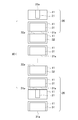
- FIG. 4 is an exploded plan view of the multilayer body 10 of the multilayer capacitor 1.
- FIG. 5 is a perspective view showing the resistance layer 40 formed on the side surface 12 of the multilayer body 10.
- the multilayer capacitor 1 includes a rectangular parallelepiped multilayer body 10 and a pair of external electrodes 50 and 51 formed on side surfaces 12 and 13 extending in the longitudinal direction of the multilayer body 10.
- the multilayer capacitor 1 is an LW inversion type multilayer ceramic capacitor in which the external electrodes 50 and 51 are arranged in the longitudinal direction so that the current path of the internal electrodes is thickened and shortened to reduce ESL.
- the multilayer body 10 is configured by alternately laminating a plurality of dielectric layers 11 formed in a rectangular shape and a plurality of internal electrodes 21, 31, and 32.
- the dielectric layer 11 is made of, for example, a dielectric ceramic mainly composed of BaTiO 3 , CaTiO 3 , SrTiO 3 , CaZrO 3 or the like. Note that subcomponents such as a Mn compound, Fe compound, Cr compound, Co compound, and Ni compound may be added to these main components.
- the plurality of internal electrodes 21, 31, and 32 have an internal electrode 21 in which the width of the lead portion 21 a (length along the longitudinal direction of the multilayer body 10) is narrow, and the width of the lead portions 31 a and 32 a is smaller than the internal electrode 21. Wide internal electrodes 31 and 32 are included.
- the internal electrodes 21 having a narrow width of the lead portion 21 a are disposed at both ends (that is, the upper and lower portions) in the stacking direction (thickness direction) of the stacked body 10.
- An internal electrode 31 and an internal electrode 32 are disposed at the center of the stacked body 10 in the stacking direction.
- the internal electrode 21, the internal electrode 31, and the internal electrode 32 are formed in a rectangular thin film as shown in FIG.
- the internal electrodes 21 or the internal electrodes 32 and the internal electrodes 31 are alternately stacked so as to face each other with the dielectric layer 11 in between.
- Each of the internal electrodes 21, 31, 32 is made of, for example, Ni, Cu, Ag, Pd, an Ag—Pd alloy, Au, or the like.
- the width of the internal electrode 21 is the same as the width of the lead portion 21a, but the width of the internal electrode 21 is, for example, the width of the lead portion 21a according to the desired capacitance. You may form larger.
- the internal electrode 21 and the internal electrode 32 are drawn out to one side surface 12 of the multilayer body 10, and the internal electrode 31 is drawn out to the other side surface 13 of the multilayer body 10.
- One side surface 12 in the longitudinal direction of the laminate 10 covers the lead portion 21a of the internal electrode 21 drawn out to the side surface 12 and covers a part of the lead portion 32a of the internal electrode 32.
- a resistance layer 40 is formed. More specifically, as shown in FIG. 5, the resistance layer 40 has a width D2 that is wider than the width D1 of the lead portion 21a of the internal electrode 21 and narrower than the width D3 of the lead portion 32a of the internal electrode 32. And is formed from the upper end to the lower end along the stacking direction of the stacked body 10. Note that a resistance layer is not formed on the other side surface 13 of the stacked body 10.
- the resistance layer 40 is formed by baking a resistance paste containing a resistance component.
- a resistance component for example, composite oxides such as In—Sn composite oxide (ITO), La—Cu composite oxide, Sr—Fe composite oxide, and Ca—Sr—Ru composite oxide are used.
- glass such as B—Si glass or B—Si—Zn glass is added to the resistance layer 40.
- specific resistance or the like may be adjusted by adding a metal such as Ni, Cu, Mo, Cr, or Nb or a metal oxide such as Al 2 O 3, TiO 2, ZrO 2, or ZnO 2 to the resistance layer 40.
- a pair of external electrodes 50 and 51 are formed on both side surfaces 12 and 13 in the longitudinal direction of the laminate 10 so as to cover the entire surfaces of the both side surfaces 12 and 13. That is, the pair of external electrodes 50 and external electrodes 51 are formed on the side surfaces 12 and 13 of the multilayer body 10 so as to face each other with the multilayer body 10 interposed therebetween.
- the external electrode 50 is connected to the lead portion 21 a of the internal electrode 21 through the resistance layer 40.
- the external electrode 50 is connected to the central portion of the lead portion 32 a of the internal electrode 32 through the resistance layer 40 and directly connected to both end portions of the lead portion 32 a of the internal electrode 32.
- the external electrode 51 is directly connected to the entire lead portion 31 a of the internal electrode 31.
- the external electrodes 50 and 51 are preferably composed of a plurality of plating layers.
- the external electrodes 50 and 51 are formed so as to go from the side surfaces 12 and 13 in the longitudinal direction to the side surfaces in the short direction perpendicular to the side surfaces 12 and 13 and the upper and lower main surfaces.
- the capacitor unit 20 formed by the internal electrode 21 and the internal electrode 31 facing the internal electrode 21 is connected to the external electrode 50 via the resistance layer 40.
- a resistance component is inserted in series with the capacitor unit 20, and the value of ESR increases.
- the capacitor unit 20 is referred to as a high ESR capacitor unit 20.
- the capacitor portion 30 formed by the internal electrode 31 and the internal electrode 32 is directly connected to the external electrode 50 at both ends of the lead portion 32a of the internal electrode 32, the value of ESR is a high ESR capacitor. It becomes smaller than the part 20.
- the capacitor unit 30 is referred to as a low ESR capacitor unit 30.
- the internal electrodes 21 are disposed at both ends in the stacking direction of the stacked body 10. Therefore, in the multilayer capacitor 1, the two high ESR capacitor portions 20, 20 are disposed at both ends in the stacking direction of the multilayer body 10, that is, the upper portion and the lower portion, and the low ESR capacitor portion 30 is interposed therebetween. .
- the ESR of the high ESR capacitor unit 20 is higher than 100 m ⁇ , and is set to, for example, about 1 ⁇ to 20 ⁇ depending on the desired power supply impedance characteristic. In the present embodiment, the ESR of the high ESR capacitor unit 20 is set to 1 ⁇ .
- the ESR value of the low ESR capacitor unit 30 is set to 100 m ⁇ or less, for example. In the present embodiment, the ESR of the low ESR capacitor unit 30 is set to 10 m ⁇ .
- the electrostatic capacity of the high ESR capacitor unit 20 formed by the internal electrode 21 connected to the external electrode 50 through the resistance layer 40 is between the power plane and the ground plane of the multilayer board on which the multilayer capacitor 1 is mounted.
- the capacitance is set substantially the same as the capacitance. For example, when the capacitance between the power plane and the ground plane of the multilayer board to be mounted is about 100 pF, the capacitance of the high ESR capacitor unit 20 is set to about 100 pF. Note that the capacitance of the high ESR capacitor unit 20 is adjusted by adjusting the area of the internal electrode 21 and the number of stacked layers, for example.
- the multilayer capacitor 1 is an LW reversal type multilayer ceramic capacitor in which the vertical and horizontal directions are reversed by arranging the external electrodes 50 and 51 in the longitudinal direction, and therefore, the ESL of the high ESR capacitor unit 20, and The ESL of the low ESR capacitor unit 30 is low (low ESL). Further, according to the multilayer capacitor 1, since the ESR of the low ESR capacitor unit 30 is low, the amount of attenuation increases (impedance decreases) in the low frequency region including the resonance frequency. Further, since the resonance frequency of the low ESR capacitor unit 30 having a large capacitance is lower than the resonance frequency of the high ESR capacitor unit 20, the resonance becomes steep and a deep attenuation amount is realized.
- the high ESR capacitor unit 20 is formed by adding resistance by the resistance layer 40 formed between the side surface 12 of the multilayer body 10 and the external electrode 50, Anti-resonance with the interplane capacitance is suppressed.
- the capacitance of the high ESR capacitor unit 20 is set to be substantially the same as the capacitance between the planes of the multilayer board to be mounted (between the power plane and the ground plane). The impedance near the antiresonance frequency is effectively reduced.
- the power impedance reduction effect (that is, the voltage fluctuation suppression effect and the noise reduction effect) by matching the capacitance of the high ESR capacitor unit 20 and the inter-plane capacitance of the multilayer substrate. )
- the insertion loss of the multilayer capacitor 1 was measured.
- the multilayer substrate on which the multilayer capacitor 1 is mounted has a power plane-ground plane capacitance of 100 pF.
- the ESR of the high ESR capacitor unit 20 is fixed to 1 ⁇
- the capacitance of the low ESR capacitor unit 30 is fixed to 0.1 ⁇ F
- the capacitance of the high ESR capacitor unit 20 is set to 1 ⁇ F, 1000 pF, and 100 pF. 47 ⁇ F and 10 pF were used.
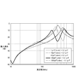
- FIG. 6 shows the insertion loss (measurement result) when the multilayer capacitor 1 in which the capacitance of the high ESR capacitor unit 20 is changed is mounted on a multilayer substrate having an interplane capacitance of 100 pF.
- the horizontal axis of the graph shown in FIG. 6 is frequency (MHz), and the vertical axis is insertion loss (dB).
- the measurement result when the capacitance of the high ESR capacitor unit 20 is matched with the inter-plane capacitance of the multilayer substrate (that is, 100 pF) is indicated by a thick solid line.
- the insertion loss when the capacitance of the high ESR capacitor 20 is 1 ⁇ F is indicated by a broken line, and the insertion loss when the capacitance is 10 pF is indicated by a one-dot chain line. Further, the insertion loss when the capacitance of the high ESR capacitor 20 is 47 pF is indicated by a thin solid line, and the insertion loss when the capacitance is 1000 pF is indicated by a two-dot chain line.
- the high ESR capacitor unit 20 is inserted both when the capacitance (1000 pF, 1 ⁇ F) is larger than the capacitance between planes (100 pF) of the multilayer substrate (47 pF, 10 pF).
- the loss peak (minimum value) has decreased (ie, the impedance has increased). That is, as shown by a thick solid line in FIG. 6, the insertion loss peak (minimum value) when the capacitance of the high ESR capacitor unit 20 is matched with the inter-plane capacitance of the multilayer substrate (that is, 100 pF). ) Is the largest (that is, the impedance is the lowest).
- the capacitor unit 20 formed by the internal electrode 21 since the internal electrode 21 is connected to the external electrode 50 via the resistance layer 40, the capacitor unit 20 formed by the internal electrode 21 has a high ESR.
- part or all of the internal electrodes 31 and 32 are directly connected to the external electrodes 50 and 51, so that the capacitor section 30 formed by the internal electrodes 31 and 32 has low ESR. Therefore, when the multilayer capacitor 1 is mounted, the current flowing from the power supply to the ground passes through the low ESR capacitor unit 30 having a small ESR value at a frequency other than the vicinity of the antiresonance frequency (including the resonance frequency).
- the impedance of the low ESR capacitor unit 30 becomes extremely large due to the antiresonance at a frequency near the antiresonance frequency, the current passes through the high ESR capacitor unit 20 having a relatively low impedance. Therefore, it is possible to reduce the impedance at the anti-resonance frequency while keeping the impedance at the resonance frequency low.
- the capacitance of the high ESR capacitor unit 20 is set to be substantially the same as the capacitance between the power plane and the ground plane of the multilayer substrate. It is possible to more effectively reduce the impedance.
- the internal electrodes 21 having the narrow lead portions 21a are disposed at both ends in the stacking direction of the multilayer body 10, so that the multilayer capacitor 1 can have vertical symmetry. . Therefore, when mounting the multilayer capacitor 1 on a substrate or the like, it is not necessary to distinguish the upper and lower directions.
- the width D2 of the resistance layer 40 is set to be wider than the width D1 of the lead portion 21a and narrower than the width D3 of the lead portion 31a, and the resistance layer 40 is stacked in the stacking direction of the stacked body 10. Is formed from the upper end to the lower end. Therefore, the resistance layer 40 can be easily formed, and the manufacturing efficiency of the multilayer capacitor 1 can be improved.
- the present invention is not limited to the above-described embodiments, and various modifications can be made.
- the internal electrodes 21 having the narrow lead portions 21a are disposed at both ends of the multilayer body 10 and the high ESR capacitor portions 20 are formed on the upper and lower portions of the multilayer body 10.
- 21 may be disposed only at the lower end of the multilayer body 10 and the high ESR capacitor portion 20 may be formed only at the lower portion of the multilayer body 10. In this way, when the multilayer capacitor 1 is mounted on the multilayer substrate, the distance between the multilayer substrate and the high ESR capacitor unit 20 is shortened, so that ESL can be reduced.
- the resistance layer 40 that is wider than the width D1 of the lead portion 21a and narrower than the width D3 of the lead portion 31a is formed from the upper end to the lower end along the stacking direction of the stacked body 10. As shown, the resistance layer 40 may be formed so as to cover only the lead portions 21 a and 21 a of the two internal electrodes 21 and 21 drawn to the side surface 12 of the multilayer body 10.
- the internal electrode 21 having the narrow lead portion 21a is drawn to the one side surface 12 of the multilayer body 10 and the resistance layer 40 is formed only on the side surface 12.
- a new internal electrode 21 may be provided so as to face each other, and a lead portion 21a of the new internal electrode 21 may be drawn to the other side surface 13 and a similar resistance layer 40 may be formed on the side surface 13.
Landscapes
- Engineering & Computer Science (AREA)
- Power Engineering (AREA)
- Manufacturing & Machinery (AREA)
- Microelectronics & Electronic Packaging (AREA)
- Chemical & Material Sciences (AREA)
- Ceramic Engineering (AREA)
- Inorganic Chemistry (AREA)
- Ceramic Capacitors (AREA)
- Fixed Capacitors And Capacitor Manufacturing Machines (AREA)
Abstract
積層コンデンサ(1)は、複数の誘電体層(11)と複数の内部電極(21,31,32)とが交互に積層された積層体(10)と、該積層体(10)の一方の長手方向の側面(12)に引き出された幅が狭い引き出し部(21a)を覆うように形成された抵抗層(40)と、積層体(10)の長手方向の対向する側面(12,13)を覆うように形成された一対の外部電極(50,51)とを備える。外部電極(50)は、内部電極(21)の引き出し部(21a)と抵抗層(40)を介して接続されるとともに、内部電極(32)の引き出し部(32a)の両端部と直接的に接続されている。また、内部電極(21)によって形成される高ESRコンデンサ部(20)の静電容量は、実装される多層基板の電源プレーン-グランドプレーン間の静電容量と略同じに設定される。
Description
本発明は、積層コンデンサに関する。
ディジタル回路では、ICやLSIの動作中の負荷変動を吸収したり、ノイズを除去するため、電源-グランド間にデカップリングコンデンサが挿入されている。電圧変動を抑制する観点から、電源インピーダンスは可能な限り低い方がよく、よってデカップリングコンデンサのインピーダンスも低いことが望ましい。
ところで、現実のコンデンサには、容量成分(ESC(Equivalent Series Capacitance))の他、等価直列インダクタンス(ESL(Equivalent Series Inductance)や等価直列抵抗(ESR(Equivalent Series Resistance))が存在する。そのため、デカップリングコンデンサが実装された多層プリント基板(以下、単に「多層基板」という)では、デカップリングコンデンサの静電容量(ESC)と、多層基板の配線等のインダクタンス(L成分)及びデカップリングコンデンサのESLとによる共振(直列共振)、及び、多層基板の電源プレーン-グランドプレーン間の静電容量と、多層基板の配線等のインダクタンス(L成分)及びデカップリングコンデンサのESLとによる反共振(並列共振)が起きる。
よって、電源インピーダンスは、共振周波数を境にして、低周波側では、周波数が高くなるに従って低くなるが、高周波側では、周波数が高くなるほど高くなる傾向を示す。すなわち、電源インピーダンスは、共振周波数付近で谷型の特性を示す。一方、電源インピーダンスは、反共振周波数を境にして、低周波側では周波数が高くなるに従って高くなるが、高周波側では周波数が高くなるほど低くなる。すなわち、反共振周波数付近で山型の特性を示す。ここで、共振周波数では、インピーダンスが極小となり低く保たれるため、電圧変動は小さくなるが、反共振周波数では、インピーダンスが極大となり高くなるため、電圧変動が大きくなる。このような反共振を抑制する方法としては、デカップリングコンデンサの等価直列抵抗を大きくする(Q値を低くする)ことが考えられる。
ここで、特許文献1には、単一のコンデンサ本体内に形成された2つのコンデンサ部を有し、高い等価直列抵抗(ESR)と低い等価直列インダクタンス(ESL)とを持った積層型チップコンデンサを用いてインピーダンス周波数特性をフラットにする技術が開示されている。この積層型チップコンデンサは、積層方向に沿って配列された第1コンデンサ部及び第2コンデンサ部を有するコンデンサ本体と、該コンデンサ本体の外側に形成された4つの外部電極を有している。また、この積層チップコンデンサは、第1コンデンサ部のESLが第2コンデンサ部のESLよりも小さくなるように、かつ、第1コンデンサ部のESRが第2コンデンサ部のESRより大きくなるように形成されている。そして、この積層型チップコンデンサが回路基板に実装される際に、第1コンデンサ部と第2コンデンサ部とが連結導体ラインを通じて相互並列に連結される。この連結導体ラインの抵抗の直列的付加により、第2コンデンサ部のESRが実質的に増大され、2つのコンデンサ部間の差異が実質的に減少される。これによって、広い周波数帯域で一定のインピーダンス特性が具現化される。
上述した技術では、ESRの小さな第2コンデンサ部について、連結導体ラインを用いてESRを増大し、第1コンデンサ部のESRに近づけることによって、広い周波数範囲でフラットなインピーダンス特性を実現している。しかしながら、フラットな特性であるがゆえに、反共振周波数でのインピーダンスは比較的低く抑えられるが、反共振周波数よりも低周波数側の領域、特に共振周波数周辺でインピーダンスが増大するという問題がある。
本発明は、上記問題点を解消する為になされたものであり、共振周波数での電源インピーダンスを低く保ったまま反共振周波数での電源インピーダンスを下げることが可能な積層コンデンサを提供することを目的とする。
本発明に係る積層コンデンサは、複数の誘電体層と、引き出し部の幅が異なる内部電極を含んで構成される複数の内部電極とが交互に積層された積層体と、積層体の少なくとも一方の長手方向の側面に、該側面に引き出された幅が異なる引き出し部のうち幅が狭い方の引き出し部を覆うように形成された抵抗層と、積層体の長手方向の対向する側面それぞれを覆うように形成された一対の外部電極とを備え、一対の外部電極は、少なくともいずれか一方が、引き出し部の幅が狭い方の内部電極と抵抗層を介して接続されるとともに、引き出し部の幅が広い方の内部電極と一部又は全部が直接的に接続されていることを特徴とする。
本発明に係る積層コンデンサによれば、引き出し部の幅が狭い内部電極は、抵抗層を介して外部電極に接続されているため、該内部電極により形成されるコンデンサ部は、ESR(等価直列抵抗)が高くなる。一方、引き出し部の幅が広い内部電極は、少なくとも一部分は直接的に外部電極に接続されているため、該内部電極により形成されるコンデンサ部は、ESRが低くなる。そのため、該積層コンデンサが実装された際に、電源からグランドに流れる電流は、反共振周波数の付近以外の周波数(共振周波数を含む)ではESRが小さい方のコンデンサ部(以下「低ESRコンデンサ部」ともいう)を通り、反共振周波数の付近の周波数ではESRが高い方のコンデンサ部(以下「高ESRコンデンサ部」ともいう)を通る。そのため、共振周波数でのインピーダンスを低く保ったまま、反共振周波数でのインピーダンスを下げることが可能となる。
本発明に係る積層コンデンサでは、抵抗層を介して外部電極と接続された引き出し部の幅が狭い方の内部電極によって形成されるコンデンサ部の静電容量が、実装される基板の電源プレーン-グランドプレーン間の静電容量と略同じ静電容量となるように設定されていることが好ましい。
この場合、高ESRコンデンサ部の静電容量が、基板の電源プレーン-グランドプレーン間の静電容量と略同一となるように設定されるため、反共振周波数付近でのインピーダンスをより効果的に低減することが可能となる。なお、ここで、基板には、プリント基板の他、インターポーザなどを含むものとする。
本発明に係る積層コンデンサでは、引き出し部の幅が狭い方の内部電極が、積層体の積層方向の下端に配設されていることが好ましい。
このようにすれば、高ESRコンデンサ部が積層方向の下端に形成されるため、積層コンデンサが基板に実装される際に、基板の実装面と高ESRコンデンサ部との距離が短くなる。そのため、ESLを低減することができる。
本発明に係る積層コンデンサでは、引き出し部の幅が狭い方の内部電極が、積層体の積層方向の両端に配設されていることが好ましい。
このようにすれば、高ESRコンデンサ部が積層方向の両端に形成されるため、積層コンデンサに上下方向の対称性を持たせることができる。そのため、積層コンデンサを基板等に実装する際に、上下の向きを区別する必要がなくなる。
本発明に係る積層コンデンサでは、上記抵抗層の幅が、幅が狭い方の引き出し部の幅よりも広く、幅が広い方の引き出し部の幅よりも狭く、かつ、当該抵抗層が、積層体の積層方向に沿って、上端から下端まで形成されていることが好ましい。
このようにすれば、抵抗層の形成を容易に行うことができるため、積層コンデンサの製造効率を向上することが可能となる。
本発明によれば、共振周波数での電源インピーダンスを低く保ったまま反共振周波数での電源インピーダンスを下げることができることが可能となる。
以下、図面を参照して本発明の好適な実施形態について詳細に説明する。なお、各図において、同一要素には同一符号を付して重複する説明を省略する。
まず、図1~5を併せて用いて、実施形態に係る積層コンデンサ1の構成について説明する。ここで、図1は、積層コンデンサ1の外観を示す斜視図である。また、図2は、図1の白抜きの矢印方向から見た、積層コンデンサ1を構成する積層体10の斜視図であり、図3は、図1のIII-III線に沿った断面図である。図4は、積層コンデンサ1の積層体10の分解平面図である。また、図5は、積層体10の側面12に形成された抵抗層40を示す斜視図である。
積層コンデンサ1は、図1に示されるように、直方体形状の積層体10と、該積層体10の長手方向に延びる側面12,13に形成された一対の外部電極50,51を備えている。積層コンデンサ1は、外部電極50,51を長手方向に配置することによって、内部電極の電流経路を太く短くし、ESLを低減したLW逆転型積層セラミックコンデンサである。
積層体10は、図2乃至図5に示されるように、矩形に形成された複数の誘電体層11と、複数の内部電極21,31,32とが交互に積層されることにより構成されている。誘電体層11は、例えば、BaTiO3、CaTiO3、SrTiO3、CaZrO3などを主成分とする誘電体セラミックから形成される。なお、これらの主成分にMn化合物、Fe化合物、Cr化合物、Co化合物、Ni化合物などの副成分が添加されていてもよい。
複数の内部電極21,31,32は、引き出し部21aの幅(積層体10の長手方向に沿った長さ)が狭い内部電極21と、該内部電極21よりも引き出し部31a,32aの幅が広い内部電極31,32とを含んでいる。引き出し部21aの幅が狭い内部電極21は、積層体10の積層方向(厚み方向)における両端(すなわち上部及び下部)に配設されている。積層体10の積層方向における中央部には、内部電極31及び内部電極32が配設されている。
内部電極21、内部電極31、及び内部電極32は、図4に示されるように、矩形の薄膜状に形成されている。内部電極21又は内部電極32と、内部電極31とは、誘電体層11を介して互いに対向するように、交互に積層されている。内部電極21,31,32それぞれは、例えば、Ni、Cu、Ag、Pd、Ag-Pd合金、Auなどから形成される。なお、図4に示した例では、内部電極21の幅を、引き出し部21aの幅と同じにしたが、内部電極21の幅は、例えば所望する静電容量に応じて、引き出し部21aの幅よりも大きく形成してもよい。
内部電極21及び内部電極32は、積層体10の一方の側面12に引き出され、内部電極31は、積層体10の他方の側面13に引き出されている。
積層体10の一方の長手方向の側面12には、該側面12に引き出された内部電極21の引き出し部21aを全て覆うように、かつ、内部電極32の引き出し部32aの一部を覆うように抵抗層40が形成されている。より具体的には、図5に示されるように、抵抗層40は、内部電極21の引き出し部21aの幅D1よりも広く、かつ、内部電極32の引き出し部32aの幅D3よりも狭い幅D2を有し、積層体10の積層方向に沿って、上端から下端に渡って形成されている。なお、積層体10の他方の側面13には、抵抗層は形成されていない。
ここで、抵抗層40は、抵抗成分を含有する抵抗ペーストを焼き付けることによって形成される。なお、抵抗成分としては、例えば、In-Sn複合酸化物(ITO)、La-Cu複合酸化物、Sr-Fe複合酸化物、Ca-Sr-Ru複合酸化物などの複合酸化物が用いられる。また、抵抗層40には、例えばB-Si系ガラス、B-Si-Zn系ガラスなどのガラスが添加される。さらに、抵抗層40に、Ni,Cu、Mo、Cr、Nbなどの金属や、Al2O3、TiO2、ZrO2、ZnO2などの金属酸化物を添加することにより、比抵抗等を調整してもよい。
上述したように、積層体10の長手方向の両側面12,13には、該両側面12,13の全面を覆うように一対の外部電極50,51が形成されている。すなわち、一対の外部電極50と外部電極51とは、積層体10を挟んで対向するように、該積層体10の側面12,13に形成されている。外部電極50は、抵抗層40を介して、内部電極21の引き出し部21aと接続されている。また、外部電極50は、抵抗層40を介して内部電極32の引き出し部32aの中央部分と接続されるとともに、該内部電極32の引き出し部32aの両端部分と直接的に接続されている。一方、外部電極51は、内部電極31の引き出し部31a全体と直接的に接続されている。
ここで、外部電極50,51は、複数のメッキ層から構成されることが好ましく、例えば、耐はんだ喰われ性を有するニッケルメッキ層と、該ニッケルメッキ層を覆うように形成されるスズメッキ層とを含んで構成される。また、外部電極50,51それぞれは、長手方向の側面12,13から、該側面12,13と直交する短手方向の側面及び上下の主面に回り込むように形成されている。
上述したように構成されることにより、内部電極21と、該内部電極21と対向する内部電極31とによって形成されるコンデンサ部20は、抵抗層40を介して外部電極50と接続されるため、該コンデンサ部20に対して抵抗成分が直列に挿入されることとなり、ESRの値が大きくなる。以下、当該コンデンサ部20を高ESRコンデンサ部20という。一方、内部電極31と内部電極32とによって形成されるコンデンサ部30は、内部電極32の引き出し部32aの両端部分が直接的に外部電極50と接続されるため、ESRの値は、高ESRコンデンサ部20よりも小さくなる。以下、当該コンデンサ部30を低ESRコンデンサ部30という。
上述したように、内部電極21は、積層体10の積層方向における両端に配設されている。そのため、積層コンデンサ1では、積層体10の積層方向における両端、すなわち上部及び下部に、2つの高ESRコンデンサ部20,20が配置され、その間に低ESRコンデンサ部30が挟まれるように配置される。
ここで、高ESRコンデンサ部20のESRは、100mΩよりも高く、例えば、所望する電源インピーダンス特性に応じて1Ω~20Ω程度に設定される。なお、本実施形態では、高ESRコンデンサ部20のESRを1Ωに設定した。一方、低ESRコンデンサ部30のESR値は、例えば、100mΩ以下に設定される。なお、本実施形態では、低ESRコンデンサ部30のESRを10mΩに設定した。
また、抵抗層40を介して外部電極50と接続された内部電極21によって形成される高ESRコンデンサ部20の静電容量は、積層コンデンサ1が実装される多層基板の電源プレーン-グランドプレーン間の静電容量と略同じ静電容量に設定される。例えば、実装される多層基板の電源プレーン-グランドプレーン間の静電容量が100pF程度である場合には、高ESRコンデンサ部20の静電容量は、100pF程度に設定される。なお、高ESRコンデンサ部20の静電容量は、例えば、内部電極21の面積や積層数などを調節することにより調節される。
以上、説明したように、積層コンデンサ1は、外部電極50,51を長手方向に配置することによって縦横を逆転させたLW逆転型の積層セラミックコンデンサであるため、高ESRコンデンサ部20のESL、及び低ESRコンデンサ部30のESLは共に低く(低ESL)なっている。また、積層コンデンサ1によれば、低ESRコンデンサ部30のESRが低いため、共振周波数を含む低周波領域では、減衰量が大きくなる(インピーダンスが小さくなる)。また、静電容量が大きい低ESRコンデンサ部30の共振周波数は、高ESRコンデンサ部20の共振周波数より低周波にあるため、共振が急峻なものとなり、深い減衰量が実現される。
一方、積層コンデンサ1では、積層体10の側面12と外部電極50との間に形成された抵抗層40によって抵抗が付加されることにより高ESRコンデンサ部20が形成されているため、多層基板のプレーン間静電容量との反共振が抑制される。
さらに、積層コンデンサ1では、高ESRコンデンサ部20の静電容量が、実装される多層基板のプレーン間(電源プレーン-グランドプレーン間)の静電容量と略同一となるように設定されているため、反共振周波数付近でのインピーダンスが効果的に低減される。
ここで、本実施形態に係る積層コンデンサ1において、高ESRコンデンサ部20の静電容量と多層基板のプレーン間容量とを一致させることによる電源インピーダンスの低減効果(すなわち電圧変動抑制効果及びノイズ低減効果)を確認するために、積層コンデンサ1の挿入損失を測定した。なお、挿入損失が大きい程、電源インピーダンスが小さく、電圧変動抑制効果及びノイズ低減効果が大きくなることを示す。
ここでは、積層コンデンサ1を実装する多層基板として、電源プレーン-グランドプレーン間容量が100pFのものを用いた。また、積層コンデンサ1として、高ESRコンデンサ部20のESRを1Ω、低ESRコンデンサ部30の静電容量を0.1μFで固定し、高ESRコンデンサ部20の静電容量を、1μF、1000pF、100pF、47μF、10pFと変化させたものを用いた。
プレーン間容量が100pFの多層基板に、高ESRコンデンサ部20の静電容量を変えた積層コンデンサ1を実装した場合の挿入損失(測定結果)を図6に示す。図6に示されたグラフの横軸は周波数(MHz)であり、縦軸は挿入損失(dB)である。また、図6のグラフでは、高ESRコンデンサ部20の静電容量を、多層基板のプレーン間容量と一致させたとき(すなわち100pFとしたとき)の測定結果を太い実線で示した。また、高ESRコンデンサ20の静電容量を1μFとしたときの挿入損失を破線で、静電容量10pFとしたときの挿入損失を一点鎖線で示した。さらに、高ESRコンデンサ20の静電容量を47pFとしたときの挿入損失を細い実線で、静電容量1000pFとしたときの挿入損失を二点鎖線でそれぞれ示した。
図6に示されるように、高ESRコンデンサ部20の静電容量を、多層基板のプレーン間容量(100pF)より大きくした場合(1000pF、1μF)も、小さくしたとき(47pF、10pF)も、挿入損失のピーク(最小値)が小さくなった(すなわちインピーダンスが大きくなった)。すなわち、図6に太い実線で示されるように、高ESRコンデンサ部20の静電容量を、多層基板のプレーン間容量と一致させたとき(すなわち100pFとしたとき)に挿入損失のピーク(最小値)が最も大きくなる(すなわちインピーダンスが最も低くなる)ことが確認された。
本実施形態によれば、内部電極21が抵抗層40を介して外部電極50に接続されているため、該内部電極21により形成されるコンデンサ部20は、ESRが高くなる。一方、内部電極31,32は、一部又は全部が直接的に外部電極50,51に接続されているため、該内部電極31,32により形成されるコンデンサ部30は、ESRが低くなる。そのため、該積層コンデンサ1が実装された際に、電源からグランドに流れる電流は、反共振周波数の付近以外の周波数(共振周波数を含む)ではESRの値が小さい低ESRコンデンサ部30を通る。一方、反共振周波数の付近の周波数では低ESRコンデンサ部30のインピーダンスは反共振により極めて大きくなるため、電流は相対的にインピーダンスの低くなる高ESRコンデンサ部20を通る。そのため、共振周波数でのインピーダンスを低く保ったまま、反共振周波数でのインピーダンスを下げることが可能となる。
また、本実施形態によれば、高ESRコンデンサ部20の静電容量が、多層基板の電源プレーン-グランドプレーン間の静電容量と略同一となるように設定されるため、反共振周波数付近でのインピーダンスをより効果的に低減することが可能となる。
本実施形態によれば、引き出し部21aの幅が狭い内部電極21が、積層体10の積層方向の両端に配設されているため、積層コンデンサ1に上下方向の対称性を持たせることができる。そのため、積層コンデンサ1を基板等に実装する際に、上下の向きを区別する必要がなくなる。
本実施形態によれば、抵抗層40の幅D2が、引き出し部21aの幅D1よりも広く、引き出し部31aの幅D3よりも狭く設定され、かつ、抵抗層40が、積層体10の積層方向に沿って、上端から下端まで形成されている。そのため、抵抗層40の形成を容易に行うことができ、積層コンデンサ1の製造効率を向上することが可能となる。
以上、本発明の実施の形態について説明したが、本発明は、上記実施形態に限定されるものではなく種々の変形が可能である。例えば、上記実施形態では、幅が狭い引き出し部21aを有する内部電極21を積層体10の両端に配設し、高ESRコンデンサ部20を積層体10の上部と下部とに形成したが、内部電極21を、積層体10の下端のみに配設し、高ESRコンデンサ部20を積層体10の下部にのみ形成する構成としてもよい。このようにすれば、積層コンデンサ1が多層基板に実装される際に、該多層基板と高ESRコンデンサ部20との距離が短くなるため、ESLを低減することができる。
上記実施形態では、引き出し部21aの幅D1よりも広く、かつ引き出し部31aの幅D3よりも狭い抵抗層40を、積層体10の積層方向に沿って、上端から下端まで形成したが、図7に示されるように、積層体10の側面12に引き出された2つの内部電極21,21の引き出し部21a,21aのみを覆うように抵抗層40を形成してもよい。
上記実施形態では、幅が狭い引き出し部21aを有する内部電極21を積層体10の一方の側面12に引き出すとともに、該側面12にのみ抵抗層40を形成する構成としたが、この内部電極21と対向するように新たな内部電極21を設け、該新たな内部電極21の引き出し部21aを他方の側面13に引き出すとともに、該側面13にも同様の抵抗層40を形成する構成としてもよい。
1 積層コンデンサ
10 積層体
11 誘電体層
20 高ESRコンデンサ部
30 低ESRコンデンサ部
21,31,32 内部電極
21a,31a,32a 引き出し部
40 抵抗層
50,51 外部電極
10 積層体
11 誘電体層
20 高ESRコンデンサ部
30 低ESRコンデンサ部
21,31,32 内部電極
21a,31a,32a 引き出し部
40 抵抗層
50,51 外部電極
Claims (5)
- 複数の誘電体層と、引き出し部の幅が異なる内部電極を含んで構成される複数の内部電極とが交互に積層された積層体と、
前記積層体の少なくとも一方の長手方向の側面に、該側面に引き出された幅が異なる前記引き出し部のうち幅が狭い方の引き出し部を覆うように形成された抵抗層と、
前記積層体の長手方向の対向する側面それぞれを覆うように形成された一対の外部電極と、を備え、
一対の前記外部電極は、少なくともいずれか一方が、引き出し部の幅が狭い方の前記内部電極と前記抵抗層を介して接続されるとともに、引き出し部の幅が広い方の前記内部電極と一部又は全部が直接的に接続されていることを特徴とする積層コンデンサ。 - 前記抵抗層を介して前記外部電極と接続された、引き出し部の幅が狭い方の前記内部電極によって形成されるコンデンサ部の静電容量は、実装される基板の電源プレーン-グランドプレーン間の静電容量と略同じ静電容量となるように設定されていることを特徴とする請求項1に記載の積層コンデンサ。
- 引き出し部の幅が狭い方の前記内部電極は、前記積層体の積層方向の下端に配設されていることを特徴とする請求項1又は2に記載の積層コンデンサ。
- 引き出し部の幅が狭い方の前記内部電極は、前記積層体の積層方向の両端に配設されていることを特徴とする請求項1又は2に記載の積層コンデンサ。
- 前記抵抗層は、その幅が、幅が狭い方の引き出し部の幅よりも広く、幅が広い方の引き出し部の幅よりも狭く、かつ、前記積層体の積層方向に沿って、上端から下端まで形成されていることを特徴とする請求項1~4のいずれか1項に記載の積層コンデンサ。
Priority Applications (1)
| Application Number | Priority Date | Filing Date | Title |
|---|---|---|---|
| JP2012556763A JP5418701B2 (ja) | 2011-02-08 | 2012-01-05 | 積層コンデンサ |
Applications Claiming Priority (2)
| Application Number | Priority Date | Filing Date | Title |
|---|---|---|---|
| JP2011-024590 | 2011-02-08 | ||
| JP2011024590 | 2011-02-08 |
Publications (1)
| Publication Number | Publication Date |
|---|---|
| WO2012108117A1 true WO2012108117A1 (ja) | 2012-08-16 |
Family
ID=46638345
Family Applications (1)
| Application Number | Title | Priority Date | Filing Date |
|---|---|---|---|
| PCT/JP2012/000027 Ceased WO2012108117A1 (ja) | 2011-02-08 | 2012-01-05 | 積層コンデンサ |
Country Status (2)
| Country | Link |
|---|---|
| JP (1) | JP5418701B2 (ja) |
| WO (1) | WO2012108117A1 (ja) |
Cited By (2)
| Publication number | Priority date | Publication date | Assignee | Title |
|---|---|---|---|---|
| JP2014096541A (ja) * | 2012-11-12 | 2014-05-22 | Murata Mfg Co Ltd | 積層コンデンサ |
| JP2017168746A (ja) * | 2016-03-17 | 2017-09-21 | 株式会社村田製作所 | 電子部品及び電子部品の製造方法 |
Citations (2)
| Publication number | Priority date | Publication date | Assignee | Title |
|---|---|---|---|---|
| JPH11297566A (ja) * | 1998-04-07 | 1999-10-29 | Murata Mfg Co Ltd | 積層セラミック電子部品 |
| JP2007234903A (ja) * | 2006-03-01 | 2007-09-13 | Tdk Corp | 積層コンデンサ及びその製造方法 |
Family Cites Families (2)
| Publication number | Priority date | Publication date | Assignee | Title |
|---|---|---|---|---|
| JPH08115844A (ja) * | 1994-10-14 | 1996-05-07 | Tokin Corp | 積層セラミックコンデンサ |
| JP4957709B2 (ja) * | 2008-11-26 | 2012-06-20 | 株式会社村田製作所 | 積層コンデンサ |
-
2012
- 2012-01-05 JP JP2012556763A patent/JP5418701B2/ja active Active
- 2012-01-05 WO PCT/JP2012/000027 patent/WO2012108117A1/ja not_active Ceased
Patent Citations (2)
| Publication number | Priority date | Publication date | Assignee | Title |
|---|---|---|---|---|
| JPH11297566A (ja) * | 1998-04-07 | 1999-10-29 | Murata Mfg Co Ltd | 積層セラミック電子部品 |
| JP2007234903A (ja) * | 2006-03-01 | 2007-09-13 | Tdk Corp | 積層コンデンサ及びその製造方法 |
Cited By (2)
| Publication number | Priority date | Publication date | Assignee | Title |
|---|---|---|---|---|
| JP2014096541A (ja) * | 2012-11-12 | 2014-05-22 | Murata Mfg Co Ltd | 積層コンデンサ |
| JP2017168746A (ja) * | 2016-03-17 | 2017-09-21 | 株式会社村田製作所 | 電子部品及び電子部品の製造方法 |
Also Published As
| Publication number | Publication date |
|---|---|
| JPWO2012108117A1 (ja) | 2014-07-03 |
| JP5418701B2 (ja) | 2014-02-19 |
Similar Documents
| Publication | Publication Date | Title |
|---|---|---|
| JP6291056B2 (ja) | 積層型コンデンサ | |
| JP5267583B2 (ja) | 積層セラミック電子部品 | |
| US9343236B2 (en) | Multilayer ceramic capacitor and board having the same mounted thereon | |
| JP3850398B2 (ja) | 積層コンデンサ | |
| JP4957709B2 (ja) | 積層コンデンサ | |
| KR101659155B1 (ko) | 적층 세라믹 커패시터 및 그 실장 기판 | |
| US10176927B2 (en) | Composite electronic component | |
| CN101310348B (zh) | 叠层电容器 | |
| JP5949476B2 (ja) | 積層コンデンサ | |
| US20080100988A1 (en) | Multilayer capacitor | |
| US20080106847A1 (en) | Multilayer capacitor | |
| WO2015037374A1 (ja) | インダクタおよび帯域除去フィルタ | |
| JP6626966B2 (ja) | 積層型コンデンサ | |
| JP2021022722A (ja) | 積層型キャパシタ及びその実装基板 | |
| JP2018206950A (ja) | コイル部品 | |
| JP4591530B2 (ja) | 積層セラミックコンデンサ | |
| JP2012164817A (ja) | 多層配線基板 | |
| CN101533713B (zh) | 贯通电容器以及贯通电容器的安装构造体 | |
| JP5418701B2 (ja) | 積層コンデンサ | |
| JP6363444B2 (ja) | 積層型コンデンサ | |
| KR20140143341A (ko) | 적층 세라믹 커패시터 및 그 실장 기판 | |
| JP2012164816A (ja) | 多層配線基板 | |
| JP5014856B2 (ja) | 積層型フィルタ | |
| JP6500832B2 (ja) | 積層コンデンサの実装構造、及び、積層コンデンサの実装方法 | |
| JP3727542B2 (ja) | 積層貫通型コンデンサ |
Legal Events
| Date | Code | Title | Description |
|---|---|---|---|
| 121 | Ep: the epo has been informed by wipo that ep was designated in this application |
Ref document number: 12744717 Country of ref document: EP Kind code of ref document: A1 |
|
| ENP | Entry into the national phase |
Ref document number: 2012556763 Country of ref document: JP Kind code of ref document: A |
|
| NENP | Non-entry into the national phase |
Ref country code: DE |
|
| 122 | Ep: pct application non-entry in european phase |
Ref document number: 12744717 Country of ref document: EP Kind code of ref document: A1 |