WO2012105648A1 - 非感光性レジスト下層膜形成組成物 - Google Patents
非感光性レジスト下層膜形成組成物 Download PDFInfo
- Publication number
- WO2012105648A1 WO2012105648A1 PCT/JP2012/052397 JP2012052397W WO2012105648A1 WO 2012105648 A1 WO2012105648 A1 WO 2012105648A1 JP 2012052397 W JP2012052397 W JP 2012052397W WO 2012105648 A1 WO2012105648 A1 WO 2012105648A1
- Authority
- WO
- WIPO (PCT)
- Prior art keywords
- group
- resist underlayer
- underlayer film
- polymer
- photosensitive resist
- Prior art date
- Legal status (The legal status is an assumption and is not a legal conclusion. Google has not performed a legal analysis and makes no representation as to the accuracy of the status listed.)
- Ceased
Links
Images



Classifications
-
- G—PHYSICS
- G03—PHOTOGRAPHY; CINEMATOGRAPHY; ANALOGOUS TECHNIQUES USING WAVES OTHER THAN OPTICAL WAVES; ELECTROGRAPHY; HOLOGRAPHY
- G03F—PHOTOMECHANICAL PRODUCTION OF TEXTURED OR PATTERNED SURFACES, e.g. FOR PRINTING, FOR PROCESSING OF SEMICONDUCTOR DEVICES; MATERIALS THEREFOR; ORIGINALS THEREFOR; APPARATUS SPECIALLY ADAPTED THEREFOR
- G03F7/00—Photomechanical, e.g. photolithographic, production of textured or patterned surfaces, e.g. printing surfaces; Materials therefor, e.g. comprising photoresists; Apparatus specially adapted therefor
- G03F7/004—Photosensitive materials
- G03F7/09—Photosensitive materials characterised by structural details, e.g. supports, auxiliary layers
- G03F7/11—Photosensitive materials characterised by structural details, e.g. supports, auxiliary layers having cover layers or intermediate layers, e.g. subbing layers
Definitions
- the present invention provides a composition for forming a non-photosensitive resist underlayer film, which has excellent alkali developability and the cross-sectional shape of a resist pattern formed in an upper layer is substantially rectangular, and a resist formed from the composition
- the present invention relates to a method for forming a resist pattern using a lower layer film.
- a process of introducing impurity ions imparting n-type or p-type conductivity into a semiconductor substrate using a resist pattern as a mask may be employed.
- the resist used in the ion implantation process has started to require a fine pattern, and an antireflection film (resist underlayer film) under the resist has become necessary.
- Patent Literature 1 and Patent Literature 2 describe compositions for forming an antireflection film that can be developed and removed simultaneously with a resist.
- This composition contains a polyamic acid and a compound having at least two epoxy groups as a crosslinking agent.
- the present invention relates to a non-photosensitive resist underlayer film forming composition for forming a resist underlayer film that is alkali-developed together when the resist film is alkali-developed after exposure, and comprising a resist pattern having a desired cross-sectional shape.
- a composition comprising a polymer, a cross-linking agent, a solvent and other optional ingredients that can be formed.
- the non-photosensitive resist underlayer film forming composition of the present invention is obtained by adding a compound having at least two specific substituents to an acrylic polymer containing an amide structure, thereby forming a resist underlayer film formed from the composition.
- a resist pattern having a substantially rectangular cross-sectional shape can be formed.
- the first aspect of the present invention is the following formula (1): (Wherein R 1 represents a hydrogen atom or a methyl group, R 2 represents an alkylene group having 1 to 3 carbon atoms or a phenylene group which may have a substituent, and R 3 represents a hydroxy group or a carboxyl group.
- a polymer having a structural unit represented by the formula :) a compound having at least two substituents selected from the group consisting of a blocked isocyanate group, a methylol group, and an alkoxymethyl group having 1 to 5 carbon atoms, and a solvent.
- a composition for forming a non-photosensitive resist underlayer film (Wherein R 1 represents a hydrogen atom or a methyl group, R 2 represents an alkylene group having 1 to 3 carbon atoms or a phenylene group which may have a substituent, and R 3 represents a hydroxy group or a carboxyl group.
- a polymer having a structural unit represented by the formula :)
- the 2nd aspect of this invention is a structural unit other than the structural unit represented by the said Formula (1), following formula (2): Wherein R 4 represents a hydrogen atom or a methyl group, Y represents a —C ( ⁇ O) —NH— group or —C ( ⁇ O) —O— group, X represents a group containing a lactone ring, adamantane A group containing a ring or a group containing a benzene ring, wherein the carbon atom of the linking group represented by Y is bonded to the main chain of the polymer, and Y represents a —C ( ⁇ O) —NH— group.
- a third aspect of the present invention is the formation of the non-photosensitive resist underlayer film according to the first aspect or the second aspect, wherein the compound having at least two substituents is contained in an amount of 1 to 40% by mass with respect to the polymer. It is a composition.
- a fourth aspect of the present invention is the non-photosensitive resist underlayer film forming composition according to any one of the first to third aspects, further comprising a crosslinking catalyst.
- the fifth aspect of the present invention is the non-photosensitive resist underlayer film forming composition according to any one of the first to fourth aspects, further comprising a surfactant.
- the composition of the present invention can be obtained by using the composition of the present invention: 1) Since the resist underlayer film to be formed has resistance to the resist solvent, intermixing with the resist film formed in the upper layer may occur. 2) Since the resist underlayer film to be formed has solubility in an alkaline developer, it can be developed and removed together with the resist film. 3) The cross-sectional shape after forming the resist pattern on the resist underlayer film is approximately rectangular. 4) Since the resist underlayer film to be formed can be removed without performing dry etching, manufacturing of a semiconductor device including a process sensitive to damage to the substrate surface by dry etching, such as an ion implantation process Applicable to.
- FIG. 3 is a cross-sectional SEM image showing the shape of a photoresist pattern obtained using the resist underlayer film forming composition prepared in Example 1.
- FIG. 4 is a cross-sectional SEM image showing the shape of a photoresist pattern obtained using the resist underlayer film forming composition prepared in Example 3.
- FIG. 6 is a cross-sectional SEM image showing the shape of a photoresist pattern obtained using the resist underlayer film forming composition prepared in Comparative Example 3.
- the polymer constituting the non-photosensitive resist underlayer film forming composition of the present invention has a structural unit represented by the formula (1).
- R 1 represents a hydrogen atom or a methyl group
- R 2 represents an alkylene group having 1 to 3 carbon atoms or a phenylene group which may have a substituent
- R 3 represents a hydroxy group or Represents a carboxyl group.
- the alkylene group having 1 to 3 carbon atoms include a methylene group, an ethylene group, and a propylene group.
- the substituent in the phenylene group that may have a substituent include an alkyl group and a halogen group. .
- the structural unit represented by the formula (1) is shown in the following formula (1-1), formula (1-2), and formula (1-3).
- the structural unit represented by the formula (1) may contain only one type of structural unit represented by the formula (1) alone or represented by the formula (1). 2 or more types of structural units may be included.
- the weight average molecular weight of the polymer is, for example, 1,000 to 200,000, preferably 3,000 to 200,00. If the weight average molecular weight of this polymer is less than 1,000, solvent resistance may be insufficient.
- the weight average molecular weight is a value obtained by using gel as a standard sample by gel permeation chromatography (GPC).
- the polymer may be a copolymer further having a structural unit represented by the formula (2).
- R 4 represents a hydrogen atom or a methyl group
- Y represents a —C ( ⁇ O) —NH— group or a —C ( ⁇ O) —O— group
- X contains a lactone ring.
- X represents a group containing a lactone ring or a group containing an adamantane ring
- the lactone ring and adamantane ring may have a substituent such as a hydroxy group or a carboxyl group.
- the lactone ring is not limited to a 5-membered ring such as ⁇ -butyrolactone, but may be a 6-membered ring such as ⁇ -valerolactone or a 7-membered ring such as ⁇ -caprolactone.
- the lactone ring may form part of a bicyclo ring or a polycycle (for example, a tricyclo ring) or may be bonded to another ring.
- the ratio of the structural unit represented by the formula (1) and the structural unit represented by the formula (2) is 99 in molar ratio. : 1 to 40:60.
- the structural unit represented by the formula (2) for example, it is possible to adjust the developing speed of the resist lower layer film and the affinity to the substrate or the upper layer film.
- the compound having at least two substituents constituting the non-photosensitive resist underlayer film forming composition of the present invention serves as a crosslinking agent, and the content thereof is, for example, 1% by mass to 40% by mass with respect to the polymer.
- the content is preferably 10% by mass to 30% by mass.
- the compound having at least two substituents has, for example, a substituent selected from the group consisting of the aforementioned blocked isocyanate group, methylol group, and alkoxymethyl group having 1 to 5 carbon atoms, but does not have an epoxy group.
- a nitrogen-containing compound or a compound having at least one aryl group examples include a phenyl group and a naphthyl group.
- having at least two substituents means that each of a blocked isocyanate group, a methylol group, or an alkoxymethyl group having 1 to 5 carbon atoms is used alone or in combination of two or more kinds of substituents in the compound. In combination, refers to a compound comprising two or more.
- the blocked isocyanate group is a compound in which an isocyanate group (—N ⁇ C ⁇ O) is blocked with an appropriate protective group.
- the blocking agent include methanol, ethanol, isopropanol, n-butanol, 2-ethoxyhexanol, 2-N, N-dimethylaminoethanol, 2-ethoxyethanol, cyclohexanol and other alcohols, phenol, o-nitrophenol.
- Phenols such as p-chlorophenol, o-cresol, m-cresol, p-cresol, lactams such as ⁇ -caprolactam, acetone oxime, methyl ethyl ketone oxime, methyl isobutyl ketone oxime, cyclohexanone oxime, acetophenone oxime, benzophenone oxime, etc.
- Oximes, pyrazoles such as pyrazole, 3,5-dimethylpyrazole and 3-methylpyrazole, and thiols such as dodecanethiol and benzenethiol. .
- the compound having at least two substituents has at least two methylol groups or alkoxymethyl groups having 1 to 5 carbon atoms as substituents
- substituents specific examples thereof include, for example, Nicalac (registered trademark) MX-280, MX-270, MX-290 (manufactured by Sanwa Chemical Co., Ltd.), CYMEL (registered trademark) 303, 1123, POWDERLINK (registered trademark) 1174 (manufactured by Nihon Cytec Industries, Ltd.), TML-BPA -MF, TML-BPAF-MF (manufactured by Honshu Chemical Industry Co., Ltd.).
- the compound having at least two substituents may be a mixture composed of two or more compounds, or a mixture containing an oligomer formed by self-condensation of the compound.
- the non-photosensitive resist underlayer film forming composition of the present invention can contain a crosslinking catalyst that promotes a crosslinking reaction as an optional component.
- the crosslinking catalyst include 5-sulfosalicylic acid, p-toluenesulfonic acid, pyridinium-p-toluenesulfonate, trifluoromethanesulfonic acid, camphorsulfonic acid, 4-chlorobenzenesulfonic acid, 4-hydroxybenzenesulfonic acid, and benzenedisulfonic acid.
- the content of the cross-linking catalyst is, for example, 0.1% by mass to 10% by mass, preferably 0% with respect to the polymer contained in the non-photosensitive resist underlayer film forming composition of the present invention. .5 mass% to 5 mass%, more preferably 1 mass% to 3 mass%.
- the composition for forming a non-photosensitive resist underlayer film of the present invention can contain a surfactant as an optional component in order to improve the coating property to the substrate.
- a surfactant include polyoxyethylene lauryl ether, polyoxyethylene stearyl ether, polyoxyethylene cetyl ether, polyoxyethylene alkyl ethers such as polyoxyethylene oleyl ether, polyoxyethylene octylphenol ether, and polyoxyethylene nonylphenol.
- Polyoxyethylene alkylaryl ethers such as ether, polyoxyethylene / polyoxypropylene block copolymers, sorbitan monolaurate, sorbitan monopalmitate, sorbitan monostearate, sorbitan monooleate, sorbitan trioleate, sorbitan tristearate
- Sorbitan fatty acid esters such as polyoxyethylene sorbitan monolaurate
- polyoxyethylene Nonionic surfactants such as polyoxyethylene sorbitan fatty acid esters such as sorbitan monopalmitate, polyoxyethylene sorbitan monostearate, polyoxyethylene sorbitan trioleate, polyoxyethylene sorbitan tristearate, Ftop (registered trademark) EF301, EF303, EF352 (manufactured by Mitsubishi Materials Electronics Chemical Co., Ltd.
- the content of the surfactant is, for example, 3% by mass or less, preferably 1% by mass or less, with respect to the polymer contained in the non-photosensitive resist underlayer film forming composition of the present invention. More preferably, it is 0.5 mass% or less.
- the non-photosensitive resist underlayer film forming composition of the present invention can contain other additives as required.
- a regulator that adjusts the solubility in a developing solution can be included.
- the regulator include 1,1,1-tris (4-hydroxyphenyl) ethane.
- the composition for forming a non-photosensitive resist underlayer film of the present invention can be prepared by dissolving each of the above components in an appropriate solvent, and is used in a uniform solution state.
- solvents include ethylene glycol monomethyl ether, ethylene glycol monoethyl ether, methyl cellosolve acetate, ethyl cellosolve acetate, diethylene glycol monomethyl ether, diethylene glycol monoethyl ether, propylene glycol, propylene glycol monomethyl ether, propylene glycol monoethyl ether.
- the ratio of the solid content in the non-photosensitive resist underlayer film forming composition of the present invention is not particularly limited as long as each component is uniformly dissolved in a solvent, and is, for example, 0.5% by mass to 50% by mass, Alternatively, it is 1 to 40% by mass, or 2 to 30% by mass.
- the solid content is the remaining component obtained by removing the solvent from the non-photosensitive resist underlayer film forming composition of the present invention.
- the prepared composition is preferably used after being filtered using a filter having a pore size of, for example, about 0.2 ⁇ m.
- the composition for forming a non-photosensitive resist underlayer film of the present invention is excellent in long-term storage stability at room temperature.
- the method for forming a resist pattern using the non-photosensitive resist underlayer film forming composition of the present invention comprises applying the composition on a semiconductor substrate and baking it to form a resist underlayer film.
- the resist film is formed on the resist underlayer film.
- Substrate for example, a semiconductor substrate such as silicon covered with a silicon oxide film, a semiconductor substrate such as silicon covered with a silicon nitride film or a silicon oxynitride film, a silicon nitride substrate, a quartz substrate, a glass substrate (non-alkali glass, low (Including alkali glass and crystallized glass), glass substrate on which an ITO film is formed, etc.] by applying the composition of the present invention by an appropriate application method such as a spinner or coater, and then heating such as a hot plate A resist underlayer film is formed by baking using means.
- an appropriate application method such as a spinner or coater
- Baking conditions are appropriately selected from baking temperatures of 80 ° C. to 250 ° C. and baking times of 0.3 minutes to 10 minutes.
- the baking temperature is 120 to 250 ° C. and the baking time is 0.5 to 5 minutes.
- the film thickness of the resist underlayer film is 0.005 ⁇ m to 3.0 ⁇ m, for example, 0.01 ⁇ m to 0.05 ⁇ m, or 0.05 ⁇ m to 0.1 ⁇ m.
- the crosslinking is insufficient and may cause intermixing with the resist film formed in the upper layer.
- the temperature during baking is higher than the above range, intermixing with the resist film may occur due to a decrease in developability or cutting of crosslinking.
- the resist film is formed on the resist underlayer film.
- the resist film can be formed by a general method, that is, coating and baking of a photoresist solution on the resist underlayer film.
- the resist used for forming the resist film is not particularly limited as long as it is sensitive to light used for exposure, and either a negative type or a positive type can be used.
- a positive photoresist comprising a novolak resin and 1,2-naphthoquinonediazide sulfonic acid ester
- a chemically amplified photoresist comprising a binder having a group that decomposes with an acid to increase the alkali dissolution rate and a photoacid generator, an acid
- a chemically amplified photoresist comprising a low molecular weight compound that decomposes by an alkali to increase the alkali dissolution rate of the photoresist, an alkali-soluble binder, and a photoacid generator; a binder having a group that decomposes by an acid to increase the alkali dissolution rate;
- Rohm and Haas Electronic Materials, Inc. trade name: APEX-E, Sumitomo Chemical Co., Ltd., trade name: PAR710, and Shin-Etsu Chemical Co., Ltd., trade name: SEPR430, Tokyo Ohka A trade name: TDUR-P3435LP manufactured by Kogyo K.K.
- a resist pattern When forming a resist pattern, exposure is performed through a mask (reticle) for forming a predetermined pattern.
- a mask for example, a KrF excimer laser or an ArF excimer laser can be used.
- post-exposure heating Post Exposure Bake
- the conditions for “post-exposure heating” are appropriately selected from heating temperatures of 80 ° C. to 150 ° C. and heating times of 0.3 minutes to 10 minutes.
- a resist pattern is formed through a step of developing with an alkaline developer. Since the resist underlayer film formed from the composition of the present invention is soluble in an alkali developer, the resist film and the resist underlayer film can be collectively developed with an alkali developer after exposure.
- alkali developer examples include aqueous solutions of alkali metal hydroxides such as potassium hydroxide and sodium hydroxide, aqueous solutions of quaternary ammonium hydroxides such as tetramethylammonium hydroxide, tetraethylammonium hydroxide and choline, ethanolamine, and propyl.
- Alkaline aqueous solutions such as amine aqueous solution, such as amine and ethylenediamine, can be mentioned as an example.
- a surfactant or the like can be added to these developers.
- the development conditions are appropriately selected from a development temperature of 5 ° C. to 50 ° C. and a development time of 10 seconds to 300 seconds.
- the resist underlayer film formed from the resist underlayer film forming composition of the present invention is easily developed at room temperature using a 2.38 mass% tetramethylammonium hydroxide aqueous solution that is widely used for developing photoresists. be able to.
- the apparatus etc. which were used for the measurement of the weight average molecular weight of the polymer obtained by the following synthesis example are shown.
- Equipment Liquid feed pump (DP-8020 manufactured by Tosoh Corporation), Degasser (SD-8022 manufactured by the company), Column oven (CO-8020 manufactured by the company), Differential refractive index detector (RI-8020 manufactured by the company), Autosampler (AS-8020 manufactured by the company)
- Example 1 (Preparation of resist underlayer film forming composition) To 0.2 g of the polymer represented by the formula (3) obtained in Synthesis Example 1, 0.04 g of an isocyanate-based crosslinking agent (trade name: Takenate [registered trademark] B-830, manufactured by Mitsui Chemicals, Inc.) is mixed. And dissolved in 15.8 g of propylene glycol monomethyl ether to prepare a solution. Then, it filtered using the polyethylene micro filter with the hole diameter of 0.2 micrometer, and prepared the resist lower layer film forming composition (solution).
- an isocyanate-based crosslinking agent trade name: Takenate [registered trademark] B-830, manufactured by Mitsui Chemicals, Inc.
- Example 2 (Preparation of resist underlayer forming composition) To 0.1 g of the polymer represented by the formula (3) obtained in Synthesis Example 1, 0.01 g of an aminoplast crosslinking agent (manufactured by Sanwa Chemical Co., Ltd., trade name: Nicalac [registered trademark] MX-280) And 0.002 g of 5-sulfosalicylic acid dihydrate as a crosslinking catalyst were mixed and dissolved in 7.4 g of propylene glycol monomethyl ether to obtain a solution. Then, it filtered using the polyethylene micro filter with the hole diameter of 0.2 micrometer, and prepared the resist lower layer film forming composition (solution).
- an aminoplast crosslinking agent manufactured by Sanwa Chemical Co., Ltd., trade name: Nicalac [registered trademark] MX-280
- 5-sulfosalicylic acid dihydrate as a crosslinking catalyst were mixed and dissolved in 7.4 g of propylene glycol monomethyl ether to obtain a solution. Then,
- Example 3> (Preparation of resist underlayer film forming composition) 0.12 g of the polymer represented by the formula (4) obtained in Synthesis Example 2 is mixed with 0.02 g of an isocyanate crosslinking agent (trade name: Takenate (registered trademark) B-830, manufactured by Mitsui Chemicals, Inc.). Then, it was dissolved in 8.5 g of propylene glycol monomethyl ether to obtain a solution. Then, it filtered using the polyethylene micro filter with the hole diameter of 0.2 micrometer, and prepared the resist lower layer film forming composition (solution).
- an isocyanate crosslinking agent trade name: Takenate (registered trademark) B-830, manufactured by Mitsui Chemicals, Inc.
- the formed silicon wafer with a film was immersed in a developer for 1 minute to confirm solubility in the developer. After immersion, the film was rinsed with water and dried by nitrogen blowing to check the remaining film. Table 1 below shows the solubility in the developer when immersed in the developer and the baking temperature at which no residual film was confirmed after development. In Table 1, when the film was uniformly dissolved during development and the residual film of the resist underlayer film could not be confirmed after development, the developer solubility was evaluated as “good”, while the resist underlayer film was not developed during development. A case where peeling of a film that did not dissolve uniformly and was not dissolved from the semiconductor substrate was observed (peeling development), or a case where a residual film was confirmed after development was evaluated as “bad”.
- each resist underlayer film forming composition prepared in Examples 1 to 3 and Comparative Examples 1 to 3 was applied onto a semiconductor substrate (silicon wafer) by a spinner. Thereafter, the resist was baked on a hot plate for 1 minute at the “baking temperature at which no remaining film was confirmed after development” shown in Table 1 to form a resist underlayer film (film thickness 0.04 ⁇ m).
- This resist underlayer film was immersed in propylene glycol monomethyl ether acetate, which is a solvent used for a photoresist, for 1 minute. The results of evaluation are also shown in Table 1 below.
- Each resist underlayer film forming composition prepared in Examples 1 to 3 and Comparative Example 3 was applied onto a semiconductor substrate (silicon wafer) by a spinner. Thereafter, baking was performed on a hot plate at 185 ° C. for Example 1 and Comparative Example 3, 130 ° C. for Example 2, and 195 ° C. for Example 3 for 1 minute to form a resist underlayer film (film thickness 0.05 ⁇ m).
- These resist underlayer films were subjected to refractive index (n value) and attenuation coefficient (k value) at wavelengths of 248 nm and 193 nm using an optical ellipsometer (manufactured by JA Woollam, VUV-VASE VU-302). It was measured. The evaluation results are shown in Table 2 below.
- Each resist underlayer film forming composition prepared in Examples 1 and 3 and Comparative Example 3 was applied onto a semiconductor substrate (silicon wafer) by a spinner. Thereafter, baking was performed on a hot plate at 185 ° C. in Example 1, 195 ° C. in Example 3, and 185 ° C. in Comparative Example 3 for 1 minute to form a resist underlayer film (film thickness: 0.04 ⁇ m).
- a commercially available photoresist solution (trade name: TDUR-P3435LP, manufactured by Tokyo Ohka Kogyo Co., Ltd.) is applied onto the resist underlayer film with a spinner and heated on a hot plate at 90 ° C. for 1 minute to form a photoresist film.
- FIG. 1 Example 1
- FIG. 2 Example 3
- FIG. 3 Comparative Example 3
- the cross-sectional shape of the obtained photoresist pattern was substantially rectangular as shown in FIGS. It was.
- the resist underlayer film forming composition prepared in Comparative Example 3 was used, the cross-sectional shape of the obtained photoresist pattern became a ridge shape in the vicinity of the interface with the resist underlayer film, and was rectangular as shown in FIG. It did not become.
Landscapes
- Engineering & Computer Science (AREA)
- Architecture (AREA)
- Structural Engineering (AREA)
- Physics & Mathematics (AREA)
- General Physics & Mathematics (AREA)
- Materials For Photolithography (AREA)
- Addition Polymer Or Copolymer, Post-Treatments, Or Chemical Modifications (AREA)
- Exposure Of Semiconductors, Excluding Electron Or Ion Beam Exposure (AREA)
Abstract
【課題】新規な非感光性レジスト下層膜形成組成物を提供する。 【解決手段】 下記式(1):(式中、R1は水素原子又はメチル基を表し、R2は炭素原子数1乃至3のアルキレン基又は置換基を有してもよいフェニレン基を表し、R3はヒドロキシ基又はカルボキシル基を表す。)で表される構造単位を有するポリマー、ブロックイソシアネート基、メチロール基及び炭素原子数1乃至5のアルコキシメチル基からなる群から選択される置換基を少なくとも2つ有する化合物、及び溶剤を含む、非感光性レジスト下層膜形成組成物。
Description
本発明は、アルカリ現像性に優れ、上層に形成されるレジストパターンの断面形状が概略矩形状となる、非感光性レジスト下層膜を形成するための組成物、及び当該組成物から形成されたレジスト下層膜を用いるレジストパターンの形成方法に関する。
半導体装置製造におけるイオン注入工程として、レジストパターンをマスクとして半導体基板に、n型又はp型の導電型を付与する不純物イオンを導入する工程が採用される場合がある。そして、その工程では、基板表面に損傷を与えることを避けるため、レジストのパターン形成の際にドライエッチングをおこなうことは望ましくない。そのため、イオン注入工程のためのレジストパターンの形成においては、レジストの下層にドライエッチングによる除去を必要とする反射防止膜を使用することができなかった。しかしながら近年の微細化に伴い、イオン注入工程で用いられるレジストにも微細なパターンが必要とされ始め、レジスト下層の反射防止膜(レジスト下層膜)が必要となってきた。
このような背景から、レジストの現像に使用されるアルカリ現像液に溶解し、レジストと同時に現像除去することができるレジスト下層膜の開発が望まれていた。例えば、特許文献1及び特許文献2には、レジストと同時に現像除去することができる反射防止膜を形成するための組成物について記載されている。この組成物は、ポリアミド酸、及び架橋剤として少なくとも2つのエポキシ基を有する化合物を含有するものである。
従来の、アルカリ現像液に溶解する非感光性レジスト下層膜は、当該レジスト下層膜上に形成するレジストパターンの断面形状を矩形状にすることが困難であった。本発明は、露光後にレジスト膜をアルカリ現像する際に、共にアルカリ現像されるレジスト下層膜を形成するための非感光性レジスト下層膜形成組成物であって、所望の断面形状を有するレジストパターンを形成できる、ポリマー、架橋剤、溶剤及びその他の任意成分からなる組成物を提供する。
本発明の非感光性レジスト下層膜形成組成物は、アミド構造を含むアクリルポリマーに、特定の置換基を少なくとも2つ有する化合物が添加されたことにより、当該組成物から形成されるレジスト下層膜上に、断面形状が概略矩形状のレジストパターンを形成できることを見出したことに基づく。
すなわち、本発明の第1態様は、下記式(1):

(式中、R1は水素原子又はメチル基を表し、R2は炭素原子数1乃至3のアルキレン基又は置換基を有してもよいフェニレン基を表し、R3はヒドロキシ基又はカルボキシル基を表す。)で表される構造単位を有するポリマー、ブロックイソシアネート基、メチロール基及び炭素原子数1乃至5のアルコキシメチル基からなる群から選択される置換基を少なくとも2つ有する化合物、及び溶剤を含む、非感光性レジスト下層膜形成組成物である。
また本発明の第2態様は、前記式(1)で表される構造単位以外の構造単位として、下記式(2):

(式中、R4は水素原子又はメチル基を表し、Yは-C(=O)-NH-基又は-C(=O)-O-基を表し、Xはラクトン環を含む基、アダマンタン環を含む基又はベンゼン環を含む基を表し、前記Yで表される連結基の炭素原子は前記ポリマーの主鎖と結合し、前記Yが-C(=O)-NH-基を表し前記Xがベンゼン環を含む基を表す場合、当該基としてヒドロキシ基又はカルボキシル基で置換されたフェニレン基は除く。)
で表される構造単位をさらに有する、第1態様に記載の非感光性レジスト下層膜形成組成物である。
本発明の第3態様は、前記置換基を少なくとも2つ有する化合物は前記ポリマーに対して1質量%乃至40質量%含まれる、第1態様又は第2態様に記載の非感光性レジスト下層膜形成組成物である。
本発明の第4態様は、架橋触媒をさらに含む、第1態様乃至第3態様のいずれかに記載の非感光性レジスト下層膜形成組成物である。
さらに本発明の第5態様は、さらに界面活性剤を含む、第1態様乃至第4態様のいずれかに記載の非感光性レジスト下層膜形成組成物である。
また本発明の第2態様は、前記式(1)で表される構造単位以外の構造単位として、下記式(2):
で表される構造単位をさらに有する、第1態様に記載の非感光性レジスト下層膜形成組成物である。
本発明の第3態様は、前記置換基を少なくとも2つ有する化合物は前記ポリマーに対して1質量%乃至40質量%含まれる、第1態様又は第2態様に記載の非感光性レジスト下層膜形成組成物である。
本発明の第4態様は、架橋触媒をさらに含む、第1態様乃至第3態様のいずれかに記載の非感光性レジスト下層膜形成組成物である。
さらに本発明の第5態様は、さらに界面活性剤を含む、第1態様乃至第4態様のいずれかに記載の非感光性レジスト下層膜形成組成物である。
本発明の組成物を用いることによって以下の効果を得ることができる:1)形成されるレジスト下層膜はレジスト溶剤に対する耐性を有するため、上層に形成されるレジスト膜とのインターミキシングが生じることがない、2)形成されるレジスト下層膜はアルカリ現像液への溶解性を有するため、前記レジスト膜と共に現像除去することができる、3)レジスト下層膜上のレジストパターン形成後の断面形状を概略矩形状とすることができる、4)形成されるレジスト下層膜はドライエッチングを行うことなく除去可能であるため、イオン注入工程など、ドライエッチングによる基板表面の損傷に敏感な工程を含む半導体素子の製造に適用できる。
本発明の非感光性レジスト下層膜形成組成物を構成するポリマーは、前記式(1)で表される構造単位を有する。
前記式(1)中、R1は水素原子又はメチル基を表し、R2は炭素原子数1乃至3のアルキレン基又は置換基を有してもよいフェニレン基を表し、R3はヒドロキシ基又はカルボキシル基を表す。
上記炭素原子数1乃至3のアルキレン基としては、メチレン基、エチレン基、プロピレン基が挙げられ、置換基を有してもよいフェニレン基における置換基としては、例えばアルキル基、ハロゲン基が挙げられる。
前記式(1)中、R1は水素原子又はメチル基を表し、R2は炭素原子数1乃至3のアルキレン基又は置換基を有してもよいフェニレン基を表し、R3はヒドロキシ基又はカルボキシル基を表す。
上記炭素原子数1乃至3のアルキレン基としては、メチレン基、エチレン基、プロピレン基が挙げられ、置換基を有してもよいフェニレン基における置換基としては、例えばアルキル基、ハロゲン基が挙げられる。
前記式(1)で表される構造単位の一例として、下記式(1-1)、式(1-2)、式(1-3)に具体例を示す。なお、前記ポリマーにおいて、前記式(1)で表される構造単位として、式(1)で表される1種の構造単位のみを単独で含んでいてもよく、或いは式(1)で表される2種以上の複数の構造単位を含んでいてもよい。

前記ポリマーの重量平均分子量は、例えば1,000乃至200,000、好ましくは3,000乃至200,00である。このポリマーの重量平均分子量が1,000より小さいと、溶剤耐性が不十分になる場合がある。なお、重量平均分子量は、ゲルパーミエーションクロマトグラフィー(GPC)により、標準試料としてポリスチレンを用いて得られる値である。
前記ポリマーは、前記式(2)で表される構造単位をさらに有する共重合体でもよい。
前記式(2)において、R4は水素原子又はメチル基を表し、Yは-C(=O)-NH-基又は-C(=O)-O-基を表し、Xはラクトン環を含む基、アダマンタン環を含む基又はベンゼン環を含む基を表す。Xがラクトン環を含む基又はアダマンタン環を含む基を表す場合、前記ラクトン環及びアダマンタン環はヒドロキシ基、カルボキシル基などの置換基を有してもよい。但し、Yが-C(=O)-NH-基を表しXがベンゼン環を含む基を表す場合、当該ベンゼン環を含む基としてヒドロキシ基又はカルボキシル基で置換されたフェニレン基は除くものとする。
上記ラクトン環は、γ-ブチロラクトンのような5員環に限らず、δ-バレロラクトンのような6員環、ε-カプロラクトンのような7員環でもよい。前記ラクトン環は、ビシクロ環又は多環(例えば、トリシクロ環)の一部を構成していても、他の環と結合していてもよい。
当該式(2)で表される構造単位の一例として、下記式(2-1)乃至式(2-9)に具体例を示す。なお、前記式(2)で表される構造単位として、式(2)で表される1種の構造単位のみを単独で含んでいてもよく、或いは式(2)で表される2種以上の複数の構造単位を含んでいてもよい。

前記式(2)において、R4は水素原子又はメチル基を表し、Yは-C(=O)-NH-基又は-C(=O)-O-基を表し、Xはラクトン環を含む基、アダマンタン環を含む基又はベンゼン環を含む基を表す。Xがラクトン環を含む基又はアダマンタン環を含む基を表す場合、前記ラクトン環及びアダマンタン環はヒドロキシ基、カルボキシル基などの置換基を有してもよい。但し、Yが-C(=O)-NH-基を表しXがベンゼン環を含む基を表す場合、当該ベンゼン環を含む基としてヒドロキシ基又はカルボキシル基で置換されたフェニレン基は除くものとする。
上記ラクトン環は、γ-ブチロラクトンのような5員環に限らず、δ-バレロラクトンのような6員環、ε-カプロラクトンのような7員環でもよい。前記ラクトン環は、ビシクロ環又は多環(例えば、トリシクロ環)の一部を構成していても、他の環と結合していてもよい。
当該式(2)で表される構造単位の一例として、下記式(2-1)乃至式(2-9)に具体例を示す。なお、前記式(2)で表される構造単位として、式(2)で表される1種の構造単位のみを単独で含んでいてもよく、或いは式(2)で表される2種以上の複数の構造単位を含んでいてもよい。
前記ポリマーにおいて、前記式(2)で表される構造単位をさらに有する場合、前記式(1)で表される構造単位と式(2)で表される構造単位の割合は、モル比で99:1乃至40:60である。
前記式(2)で表される構造単位をさらに有することにより、例えば、レジスト下層膜の現像速度の調整、及び基板又は上層膜との親和性の調整を行うことが可能となる。
前記式(2)で表される構造単位をさらに有することにより、例えば、レジスト下層膜の現像速度の調整、及び基板又は上層膜との親和性の調整を行うことが可能となる。
本発明の非感光性レジスト下層膜形成組成物を構成する、前記置換基を少なくとも2つ有する化合物は、架橋剤としてはたらき、その含有量は、前記ポリマーに対し例えば1質量%乃至40質量%、好ましくは10質量%乃至30質量%である。
前記置換基を少なくとも2つ有する化合物は、例えば、前述のブロックイソシアネート基、メチロール基及び炭素原子数1乃至5のアルコキシメチル基からなる群から選択される置換基を有するがエポキシ基を有さない、含窒素化合物又はアリール基を少なくとも1つ有する化合物である。前記アリール基としては、例えばフェニル基、ナフチル基が挙げられる。
なお本明細書において、置換基を少なくとも2つ有するとは、化合物中にブロックイソシアネート基、メチロール基、又は炭素原子数1乃至5のアルコキシメチル基のそれぞれを単独でまたは2種以上の置換基を組み合わせて、2つ以上を含む化合物を指す。
前記置換基を少なくとも2つ有する化合物は、例えば、前述のブロックイソシアネート基、メチロール基及び炭素原子数1乃至5のアルコキシメチル基からなる群から選択される置換基を有するがエポキシ基を有さない、含窒素化合物又はアリール基を少なくとも1つ有する化合物である。前記アリール基としては、例えばフェニル基、ナフチル基が挙げられる。
なお本明細書において、置換基を少なくとも2つ有するとは、化合物中にブロックイソシアネート基、メチロール基、又は炭素原子数1乃至5のアルコキシメチル基のそれぞれを単独でまたは2種以上の置換基を組み合わせて、2つ以上を含む化合物を指す。
前記置換基を少なくとも2つ有する化合物が、置換基としてブロックイソシアネート基を少なくとも2つ有する場合、その具体例としては、例えばタケネート〔登録商標〕B-830、同B-870N(三井化学(株)製)、VESTANAT〔登録商標〕B1358/100(エボニック デグサ社製)が挙げられる。
前記ブロックイソシアネート基とは、イソシアネート基(-N=C=O)が適当な保護基によりブロックされた化合物である。ブロック剤としては、例えば、メタノール、エタノール、イソプロパノール、n-ブタノール、2-エトキシヘキサノール、2-N,N-ジメチルアミノエタノール、2-エトキシエタノール、シクロヘキサノール等のアルコール類、フェノール、o-ニトロフェノール、p-クロロフェノール、o-クレゾール、m-クレゾール、p-クレゾール等のフェノール類、ε-カプロラクタム等のラクタム類、アセトンオキシム、メチルエチルケトンオキシム、メチルイソブチルケトンオキシム、シクロヘキサノンオキシム、アセトフェノンオキシム、ベンゾフェノンオキシム等のオキシム類、ピラゾール、3,5-ジメチルピラゾール、3-メチルピラゾール等のピラゾール類、ドデカンチオール、ベンゼンチオール等のチオール類が挙げられる。
前記置換基を少なくとも2つ有する化合物が、置換基としてメチロール基又は炭素原子数1乃至5のアルコキシメチル基を少なくとも2つ有する場合、その具体例としては、例えばニカラック〔登録商標〕MX-280、同MX-270、同MX-290((株)三和ケミカル製)、CYMEL〔登録商標〕303、同1123、POWDERLINK〔登録商標〕1174(以上、日本サイテックインダストリーズ(株)製)、TML-BPA-MF、TML-BPAF-MF(以上、本州化学工業(株)製)が挙げられる。
前記置換基を少なくとも2つ有する化合物は、2種以上の化合物からなる混合物であってもよく、当該化合物が自己縮合してなるオリゴマーを含む混合物であってもよい。
本発明の非感光性レジスト下層膜形成組成物は、架橋反応を促進する架橋触媒を任意成分として含むことができる。前記架橋触媒としては、例えば5-スルホサリチル酸、p-トルエンスルホン酸、ピリジニウム-p-トルエンスルホネート、トリフルオロメタンスルホン酸、カンファースルホン酸、4-クロロベンゼンスルホン酸、4-ヒドロキシベンゼンスルホン酸、ベンゼンジスルホン酸、1-ナフタレンスルホン酸、サリチル酸、クエン酸、安息香酸、ヒドロキシ安息香酸が挙げられる。これらの架橋触媒は単独で添加してもよいし、また2種以上の組合せで添加することもできる。
上記架橋触媒が使用される場合、当該架橋触媒の含有量は、本発明の非感光性レジスト下層膜形成組成物に含まれるポリマーに対し、例えば0.1質量%乃至10質量%、好ましくは0.5質量%乃至5質量%、より好ましくは1質量%乃至3質量%である。
本発明の非感光性レジスト下層膜形成組成物は、任意成分として、基板に対する塗布性を向上させるために界面活性剤を含むことができる。前記界面活性剤としては、例えばポリオキシエチレンラウリルエーテル、ポリオキシエチレンステアリルエーテル、ポリオキシエチレンセチルエーテル、ポリオキシエチレンオレイルエーテル等のポリオキシエチレンアルキルエーテル類、ポリオキシエチレンオクチルフェノールエーテル、ポリオキシエチレンノニルフェノールエーテル等のポリオキシエチレンアルキルアリールエーテル類、ポリオキシエチレン・ポリオキシプロピレンブロックコポリマー類、ソルビタンモノラウレート、ソルビタンモノパルミテート、ソルビタンモノステアレート、ソルビタンモノオレエート、ソルビタントリオレエート、ソルビタントリステアレート等のソルビタン脂肪酸エステル類、ポリオキシエチレンソルビタンモノラウレート、ポリオキシエチレンソルビタンモノパルミテート、ポリオキシエチレンソルビタンモノステアレート、ポリオキシエチレンソルビタントリオレエート、ポリオキシエチレンソルビタントリステアレート等のポリオキシエチレンソルビタン脂肪酸エステル類等のノニオン系界面活性剤、エフトップ〔登録商標〕EF301、同EF303、同EF352(三菱マテリアル電子化成株式会社(旧(株)ジェムコ)製)、メガファック〔登録商標〕F171、同F173、同R30(DIC株式会社(旧大日本インキ化学工業(株))製)、フロラードFC430、同FC431(住友スリーエム(株)製)、アサヒガード〔登録商標〕AG710、サーフロン〔登録商標〕S-382、同SC101、同SC102、同SC103、同SC104、同SC105、同SC106(旭硝子(株)製)等のフッ素系界面活性剤、オルガノシロキサンポリマーKP341(信越化学工業(株)製)等を挙げることができる。これらの界面活性剤は単独で添加してもよいし、また2種以上の組合せで添加することもできる。
上記界面活性剤が使用される場合、当該界面活性剤の含有量は、本発明の非感光性レジスト下層膜形成組成物に含まれるポリマーに対し、例えば3質量%以下、好ましくは1質量%以下、より好ましくは0.5質量%以下である。
本発明の非感光性レジスト下層膜形成組成物は、必要に応じて、その他の添加剤を含有することができる。例えば、現像液に対する溶解性を調整する調整剤を含むことができ、当該調整剤としては、例えば1,1,1-トリス(4-ヒドロキシフェニル)エタンが挙げられる。
本発明の非感光性レジスト下層膜形成組成物は、上記各成分を適当な溶剤に溶解させることによって調製でき、均一な溶液状態で用いられる。そのような溶剤としては、例えば、エチレングリコールモノメチルエーテル、エチレングリコールモノエチルエーテル、メチルセロソルブアセテート、エチルセロソルブアセテート、ジエチレングリコールモノメチルエーテル、ジエチレングリコールモノエチルエーテル、プロピレングリコール、プロピレングリコールモノメチルエーテル、プロピレングリコールモノエチルエーテル、プロピレングリコールモノメチルエーテルアセテート、プロピレングリコールプロピルエーテルアセテート、トルエン、キシレン、メチルエチルケトン、シクロペンタノン、シクロヘキサノン、2-ヒドロキシプロピオン酸エチル、2-ヒドロキシ-2-メチルプロピオン酸エチル、エトキシ酢酸エチル、ヒドロキシ酢酸エチル、2-ヒドロキシ-3-メチルブタン酸メチル、3-メトキシプロピオン酸メチル、3-メトキシプロピオン酸エチル、3-エトキシプロピオン酸エチル、3-エトキシプロピオン酸メチル、ピルビン酸メチル、ピルビン酸エチル、酢酸エチル、酢酸ブチル、乳酸エチル、乳酸ブチル、N,N-ジメチルホルムアミド、N,N-ジメチルアセトアミド、及びN-メチル-2-ピロリドンを用いることができる。これらの溶剤は単独または2種以上の組合せで使用することができる。さらに、これらの溶剤に、プロピレングリコールモノブチルエーテル、プロピレングリコールモノブチルエーテルアセテート等の高沸点溶剤を混合して使用することもできる。
本発明の非感光性レジスト下層膜形成組成物における固形分の割合は、各成分が均一に溶剤に溶解している限り特に限定はないが、例えば0.5質量%乃至50質量%であり、または1質量%乃至40質量%であり、または2質量%乃至30質量%である。前記固形分は、本発明の非感光性レジスト下層膜形成組成物から溶剤を取り除いた残りの成分である。
調製した組成物は、孔径が例えば0.2μm程度のフィルタなどを用いてろ過した後、使用することが好ましい。本発明の非感光性レジスト下層膜形成組成物は、室温で長期間の貯蔵安定性にも優れる。
本発明の非感光性レジスト下層膜形成組成物を用いたレジストパターンの形成方法は、半導体基板上に当該組成物を塗布しベークしてレジスト下層膜を形成し、前記レジスト下層膜上にレジスト膜を形成し、前記レジスト下層膜と前記レジスト膜で被覆された半導体基板を露光し、露光後に前記レジスト膜と前記レジスト下層膜を現像する工程を有する。
以下、本発明の非感光性レジスト下層膜形成組成物の使用について詳細に説明する。基板〔例えば、酸化珪素膜で被覆されたシリコン等の半導体基板、窒化珪素膜又は酸化窒化珪素膜で被覆されたシリコン等の半導体基板、窒化珪素基板、石英基板、ガラス基板(無アルカリガラス、低アルカリガラス、結晶化ガラスを含む)、ITO膜が形成されたガラス基板等〕の上に、スピナー、コーター等の適当な塗布方法により本発明の組成物を塗布し、その後、ホットプレート等の加熱手段を用いてベークすることによりレジスト下層膜が形成される。ベーク条件としては、ベーク温度80℃乃至250℃、ベーク時間0.3分乃至10分間の中から適宜、選択される。好ましくは、ベーク温度120℃乃至250℃、ベーク時間0.5分乃至5分間である。ここで、レジスト下層膜の膜厚としては、0.005μm乃至3.0μm、例えば0.01μm乃至0.05μm、又は0.05μm乃至0.1μmである。
ベーク時の温度が、上記範囲より低い場合には架橋が不十分となり、上層に形成されるレジスト膜とインターミキシングを起こすことがある。一方、ベーク時の温度が上記範囲より高い場合は現像性の低下や架橋の切断により、当該レジスト膜とのインターミキシングを起こすことがある。
次いで前記レジスト下層膜の上に、レジスト膜を形成する。レジスト膜の形成は一般的な方法、すなわち、フォトレジスト溶液のレジスト下層膜上への塗布及びベークによって行なうことができる。
前記レジスト膜の形成に使用するレジストとしては、露光に使用される光に感光するものであれば特に限定はなく、ネガ型、ポジ型いずれも使用できる。例えばノボラック樹脂と1,2-ナフトキノンジアジドスルホン酸エステルとからなるポジ型フォトレジスト、酸により分解してアルカリ溶解速度を上昇させる基を有するバインダーと光酸発生剤からなる化学増幅型フォトレジスト、酸により分解してフォトレジストのアルカリ溶解速度を上昇させる低分子化合物とアルカリ可溶性バインダーと光酸発生剤とからなる化学増幅型フォトレジスト、酸により分解してアルカリ溶解速度を上昇させる基を有するバインダーと酸により分解してフォトレジストのアルカリ溶解速度を上昇させる低分子化合物と光酸発生剤からなる化学増幅型フォトレジストなどがある。例えば、ローム・アンド・ハース・エレクトロニック・マテリアルズ社製,商品名:APEX-E、住友化学(株)製,商品名:PAR710、及び信越化学工業(株)製,商品名:SEPR430、東京応化工業(株)製,商品名:TDUR-P3435LPが挙げられる。
レジストパターンを形成する際、所定のパターンを形成するためのマスク(レチクル)を通して露光が行なわれる。露光には、例えば、KrFエキシマレーザー、ArFエキシマレーザーを使用することができる。露光後、必要に応じて露光後加熱(Post Exposure Bake)が行なわれる。“露光後加熱”の条件としては、加熱温度80℃乃至150℃、加熱時間0.3分乃至10分間の中から適宜、選択される。その後、アルカリ現像液で現像する工程を経て、レジストパターンが形成される。本発明の組成物から形成されたレジスト下層膜は、アルカリ現像液に可溶であるため、露光を行った後、アルカリ現像液でレジスト膜及びレジスト下層膜両層の一括現像が可能である。
前記アルカリ現像液としては、水酸化カリウム、水酸化ナトリウムなどのアルカリ金属水酸化物の水溶液、水酸化テトラメチルアンモニウム、水酸化テトラエチルアンモニウム、コリンなどの水酸化四級アンモニウムの水溶液、エタノールアミン、プロピルアミン、エチレンジアミンなどのアミン水溶液等のアルカリ性水溶液を例として挙げることができる。さらに、これらの現像液に界面活性剤などを加えることもできる。
現像の条件としては、現像温度5℃乃至50℃、現像時間10秒乃至300秒から適宜選択される。本発明のレジスト下層膜形成組成物から形成されるレジスト下層膜は、フォトレジストの現像に汎用されている2.38質量%の水酸化テトラメチルアンモニウム水溶液を用いて、室温で容易に現像を行なうことができる。
以下、本発明の非感光性レジスト下層膜形成組成物の具体例を、下記実施例を用いて説明するが、これによって本発明が限定されるものではない。
下記合成例で得られたポリマーの重量平均分子量の測定に用いた装置等を示す。
装置:送液ポンプ(東ソー(株)製DP-8020)、デガッサー(同社製SD-8022)、カラムオーブン(同社製CO-8020)、示差屈折率検出器(同社製RI-8020)、オートサンプラー(同社製AS-8020)
GPCカラム:Asahipak〔登録商標〕GF-310HQ、同GF-510HQ、同GF-710HQ
カラム温度:40℃
流量:0.6ml/分
溶離液:10mmol/l LiBr/DMF
装置:送液ポンプ(東ソー(株)製DP-8020)、デガッサー(同社製SD-8022)、カラムオーブン(同社製CO-8020)、示差屈折率検出器(同社製RI-8020)、オートサンプラー(同社製AS-8020)
GPCカラム:Asahipak〔登録商標〕GF-310HQ、同GF-510HQ、同GF-710HQ
カラム温度:40℃
流量:0.6ml/分
溶離液:10mmol/l LiBr/DMF
<合成例1>
4-ヒドロキシフェニルメタクリルアミド8.0g、γ-ブチロラクトンメタクリレート3.3g、2,2’-アゾビスイソブチロニトリル0.8gをプロピレングリコールモノメチルエーテル150gに溶解させた後、この溶液をプロピレングリコールモノメチルエーテル180gが加熱還流されているフラスコ中に2時間かけて滴下した。その後、酢酸エチルを用いてポリマーを沈殿させ、ポリマーを減圧下で乾燥し、下記式(3)で表される構造単位を有するポリマーを10g得た。得られたポリマーの重量平均分子量は標準ポリスチレン換算で9,000であった。
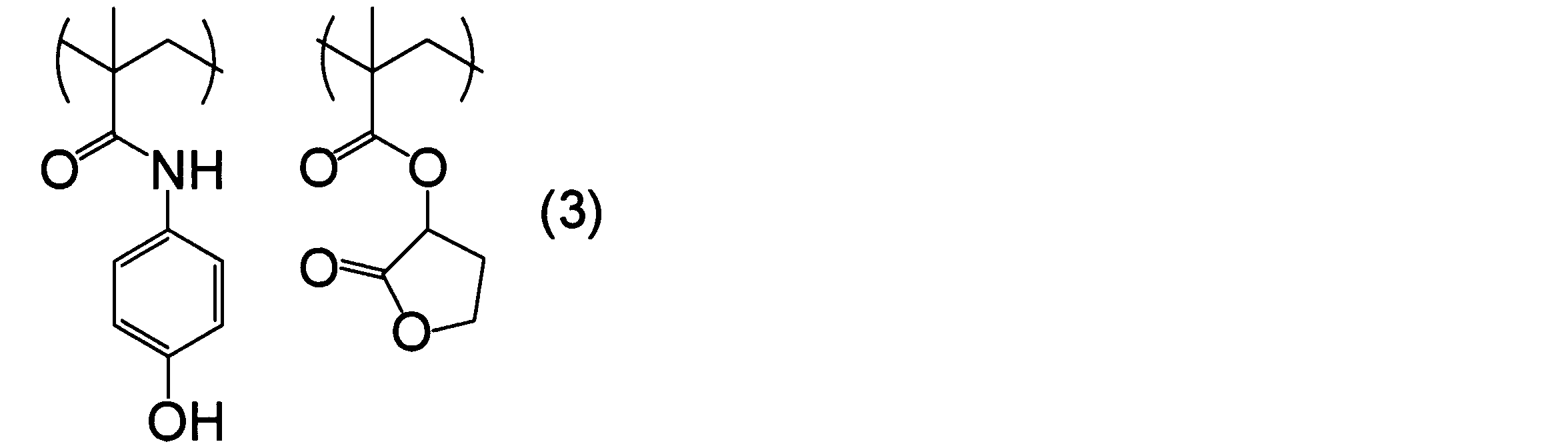
4-ヒドロキシフェニルメタクリルアミド8.0g、γ-ブチロラクトンメタクリレート3.3g、2,2’-アゾビスイソブチロニトリル0.8gをプロピレングリコールモノメチルエーテル150gに溶解させた後、この溶液をプロピレングリコールモノメチルエーテル180gが加熱還流されているフラスコ中に2時間かけて滴下した。その後、酢酸エチルを用いてポリマーを沈殿させ、ポリマーを減圧下で乾燥し、下記式(3)で表される構造単位を有するポリマーを10g得た。得られたポリマーの重量平均分子量は標準ポリスチレン換算で9,000であった。
<合成例2>
4-ヒドロキシフェニルメタクリルアミド5.0g、N-フェニルメタクリルアミド0.8g、2,2’-アゾビスイソブチロニトリル0.6gをプロピレングリコールモノメチルエーテル17gに溶解させた後、この溶液を80℃の加熱下で15時間攪拌した。その後、酢酸エチルを用いてポリマーを沈殿させ、ポリマーを減圧下で乾燥し、下記式(5)で表される構造単位を有するポリマーを5g得た。得られたポリマーの重量平均分子量は標準ポリスチレン換算で11,000であった。
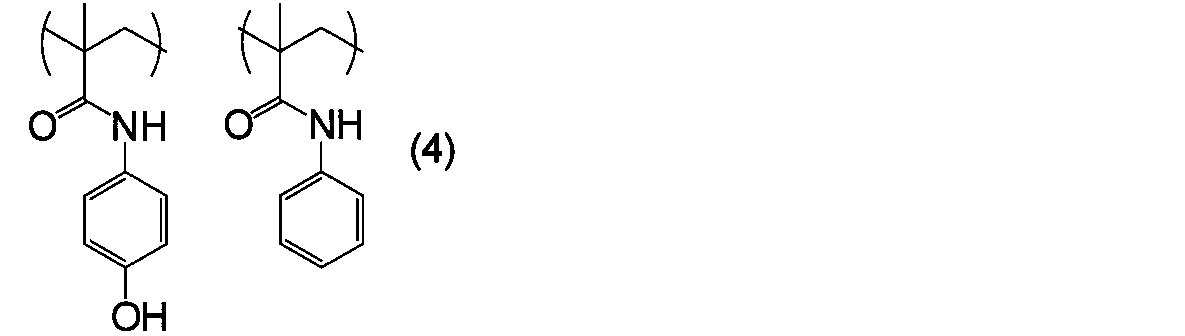
4-ヒドロキシフェニルメタクリルアミド5.0g、N-フェニルメタクリルアミド0.8g、2,2’-アゾビスイソブチロニトリル0.6gをプロピレングリコールモノメチルエーテル17gに溶解させた後、この溶液を80℃の加熱下で15時間攪拌した。その後、酢酸エチルを用いてポリマーを沈殿させ、ポリマーを減圧下で乾燥し、下記式(5)で表される構造単位を有するポリマーを5g得た。得られたポリマーの重量平均分子量は標準ポリスチレン換算で11,000であった。
<合成例3>
4-ヒドロキシフェニルメタクリレート(昭和高分子(株))5.0g、γ-ブチロラクトンメタクリレート2.0g、2,2’-アゾビスイソブチロニトリル0.5gをプロピレングリコールモノメチルエーテル30gに溶解させた後、この溶液をプロピレングリコールモノメチルエーテル113gが加熱還流されているフラスコ中に2時間かけて滴下した。その後、酢酸エチル:ヘキサン=6:4混合溶液を用いてポリマーを沈殿させ、ポリマーを減圧下で乾燥し、下記式(4)で表される構造単位を有するポリマーを5g得た。得られたポリマーの重量平均分子量は標準ポリスチレン換算で13,000であった。
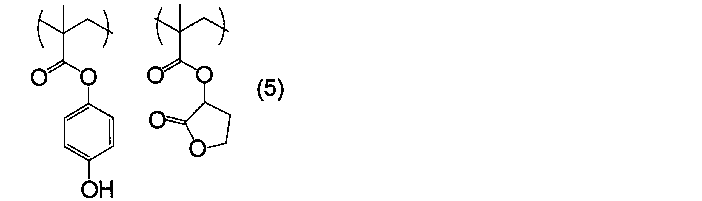
4-ヒドロキシフェニルメタクリレート(昭和高分子(株))5.0g、γ-ブチロラクトンメタクリレート2.0g、2,2’-アゾビスイソブチロニトリル0.5gをプロピレングリコールモノメチルエーテル30gに溶解させた後、この溶液をプロピレングリコールモノメチルエーテル113gが加熱還流されているフラスコ中に2時間かけて滴下した。その後、酢酸エチル:ヘキサン=6:4混合溶液を用いてポリマーを沈殿させ、ポリマーを減圧下で乾燥し、下記式(4)で表される構造単位を有するポリマーを5g得た。得られたポリマーの重量平均分子量は標準ポリスチレン換算で13,000であった。
<合成例4>
(ポリアミド酸の合成)
4,4’-(ヘキサフルオロイソプロピリデン)ビスフタル酸二無水物17.8g、3,5-ジアミノ安息香酸3.12g、ビス(4-アミノフェニル)スルホン4.92gをプロピレングリコールモノメチルエーテル145.6g中、80℃で20時間反応させることによって、ポリアミド酸を含む溶液[A]を得た。得られたポリアミド酸は、下記式(6)及び式(7)で表される構造単位を有し、重量平均分子量は標準ポリスチレン換算で2,400であった。
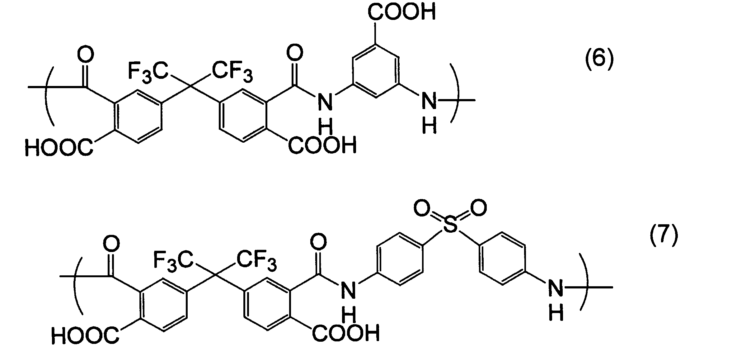
(ポリアミド酸の合成)
4,4’-(ヘキサフルオロイソプロピリデン)ビスフタル酸二無水物17.8g、3,5-ジアミノ安息香酸3.12g、ビス(4-アミノフェニル)スルホン4.92gをプロピレングリコールモノメチルエーテル145.6g中、80℃で20時間反応させることによって、ポリアミド酸を含む溶液[A]を得た。得られたポリアミド酸は、下記式(6)及び式(7)で表される構造単位を有し、重量平均分子量は標準ポリスチレン換算で2,400であった。
<合成例5>
(吸光性化合物の合成)
3,7-ジヒドロキシ-2-ナフトエ酸19.0g、トリス(2,3-エポキシプロピル)イソシアヌレート10g及びベンジルトリエチルアンモニウムクロリド0.552gをシクロヘキサノン118g中130℃で24時間反応させることで吸光性化合物(下記式(8)で表される化合物)を含む溶液[a]を得た。

(吸光性化合物の合成)
3,7-ジヒドロキシ-2-ナフトエ酸19.0g、トリス(2,3-エポキシプロピル)イソシアヌレート10g及びベンジルトリエチルアンモニウムクロリド0.552gをシクロヘキサノン118g中130℃で24時間反応させることで吸光性化合物(下記式(8)で表される化合物)を含む溶液[a]を得た。
<実施例1>
(レジスト下層膜形成組成物の調製)
合成例1で得られた式(3)で表されるポリマー0.2gに、イソシアネート系架橋剤(三井化学(株)製、商品名:タケネート〔登録商標〕B-830)0.04gを混合し、プロピレングリコールモノメチルエーテル15.8gに溶解させ溶液とした。その後、孔径0.2μmのポリエチレン製ミクロフィルタを用いてろ過し、レジスト下層膜形成組成物(溶液)を調製した。
(レジスト下層膜形成組成物の調製)
合成例1で得られた式(3)で表されるポリマー0.2gに、イソシアネート系架橋剤(三井化学(株)製、商品名:タケネート〔登録商標〕B-830)0.04gを混合し、プロピレングリコールモノメチルエーテル15.8gに溶解させ溶液とした。その後、孔径0.2μmのポリエチレン製ミクロフィルタを用いてろ過し、レジスト下層膜形成組成物(溶液)を調製した。
<実施例2>
(レジスト下層形成組成物の調製)
合成例1で得られた式(3)で表されるポリマー0.1gに、アミノプラスト系架橋剤((株)三和ケミカル製、商品名:ニカラック〔登録商標〕MX-280)0.01g、及び架橋触媒として5-スルホサリチル酸二水和物0.002gを混合し、プロピレングリコールモノメチルエーテル7.4gに溶解させ溶液とした。その後、孔径0.2μmのポリエチレン製ミクロフィルタを用いてろ過し、レジスト下層膜形成組成物(溶液)を調製した。
(レジスト下層形成組成物の調製)
合成例1で得られた式(3)で表されるポリマー0.1gに、アミノプラスト系架橋剤((株)三和ケミカル製、商品名:ニカラック〔登録商標〕MX-280)0.01g、及び架橋触媒として5-スルホサリチル酸二水和物0.002gを混合し、プロピレングリコールモノメチルエーテル7.4gに溶解させ溶液とした。その後、孔径0.2μmのポリエチレン製ミクロフィルタを用いてろ過し、レジスト下層膜形成組成物(溶液)を調製した。
<実施例3>
(レジスト下層膜形成組成物の調製)
合成例2で得られた式(4)で表されるポリマー0.1gに、イソシアネート系架橋剤(三井化学(株)製、商品名:タケネート〔登録商標〕B-830)0.02gを混合し、プロピレングリコールモノメチルエーテル8.5gに溶解させ溶液とした。その後、孔径0.2μmのポリエチレン製ミクロフィルタを用いてろ過し、レジスト下層膜形成組成物(溶液)を調製した。
(レジスト下層膜形成組成物の調製)
合成例2で得られた式(4)で表されるポリマー0.1gに、イソシアネート系架橋剤(三井化学(株)製、商品名:タケネート〔登録商標〕B-830)0.02gを混合し、プロピレングリコールモノメチルエーテル8.5gに溶解させ溶液とした。その後、孔径0.2μmのポリエチレン製ミクロフィルタを用いてろ過し、レジスト下層膜形成組成物(溶液)を調製した。
<比較例1>
(レジスト下層膜形成組成物の調製)
合成例3で得られた式(5)で表されるポリマー0.2gに、イソシアネート系架橋剤(三井化学(株)製、商品名:タケネート〔登録商標〕B-830)0.04gを混合し、プロピレングリコールモノメチルエーテル15.8gに溶解させ溶液とした。その後、孔径0.2μmのポリエチレン製ミクロフィルタを用いてろ過し、レジスト下層膜形成組成物(溶液)を調製した。
(レジスト下層膜形成組成物の調製)
合成例3で得られた式(5)で表されるポリマー0.2gに、イソシアネート系架橋剤(三井化学(株)製、商品名:タケネート〔登録商標〕B-830)0.04gを混合し、プロピレングリコールモノメチルエーテル15.8gに溶解させ溶液とした。その後、孔径0.2μmのポリエチレン製ミクロフィルタを用いてろ過し、レジスト下層膜形成組成物(溶液)を調製した。
<比較例2>
(レジスト下層膜形成組成物の調製)
合成例3で得られた式(5)で表されるポリマー0.1gに、アミノプラスト系架橋剤((株)三和ケミカル製、商品名:ニカラック〔登録商標〕MX-280)0.01g、5-スルホサリチル酸二水和物0.002gを混合し、プロピレングリコールモノメチルエーテル7.4gに溶解させ溶液とした。その後、孔径0.2μmのポリエチレン製ミクロフィルタを用いてろ過し、レジスト下層膜形成組成物(溶液)を調製した。
(レジスト下層膜形成組成物の調製)
合成例3で得られた式(5)で表されるポリマー0.1gに、アミノプラスト系架橋剤((株)三和ケミカル製、商品名:ニカラック〔登録商標〕MX-280)0.01g、5-スルホサリチル酸二水和物0.002gを混合し、プロピレングリコールモノメチルエーテル7.4gに溶解させ溶液とした。その後、孔径0.2μmのポリエチレン製ミクロフィルタを用いてろ過し、レジスト下層膜形成組成物(溶液)を調製した。
<比較例3>
(レジスト下層膜形成組成物の調製)
合成例4で得られたポリアミド酸を含む溶液[A]20gに、合成例5で得られた吸光性化合物を含む溶液[a]6.5g、トリスヒドロキシフェニルエタン0.3g、エポキシ系架橋剤(東都化成(株)製、商品名:YH434L)1.1g、プロピレングリコールモノメチルエーテル121g、プロピレングリコールモノメチルエーテルアセテート154g、シクロヘキサノン11gを添加し、室温で30分間攪拌することによりレジスト下層膜形成組成物(溶液)を調製した。
(レジスト下層膜形成組成物の調製)
合成例4で得られたポリアミド酸を含む溶液[A]20gに、合成例5で得られた吸光性化合物を含む溶液[a]6.5g、トリスヒドロキシフェニルエタン0.3g、エポキシ系架橋剤(東都化成(株)製、商品名:YH434L)1.1g、プロピレングリコールモノメチルエーテル121g、プロピレングリコールモノメチルエーテルアセテート154g、シクロヘキサノン11gを添加し、室温で30分間攪拌することによりレジスト下層膜形成組成物(溶液)を調製した。
〔レジスト下層膜の現像性評価及びフォトレジスト溶剤への溶出試験〕
現像液(東京応化工業(株)製、商品名:NMD-3、2.38質量%水酸化テトラメチルアンモニウム水溶液)に対する溶解性を評価した。実施例1乃至実施例3並びに比較例1乃至比較例3で調製された各レジスト下層膜形成組成物を、スピナーにより、半導体基板(シリコンウェハー)上に塗布した。その後、ホットプレート上で130℃から195℃まで5℃刻みの温度で1分間半導体基板をベークし、レジスト下層膜(膜厚0.04μm)を形成した。形成した膜付きシリコンウェハーを現像液へ1分間浸漬し、現像液への溶解性を確認した。浸漬後に水ですすぎ、窒素ブローにより乾燥させ、残膜を確認した。下記表1に、現像液へ浸漬した際の現像液への溶解性及び、現像後に残膜が確認されなかったベーク温度を示す。表1において、現像時に膜が均一に溶解し、かつ現像後にレジスト下層膜の残膜が確認できなかった場合を現像液溶解性が“良好”と評価し、一方、前記レジスト下層膜が現像時に均一に溶解せず、半導体基板から溶解しなかった膜の剥離が観察される(剥離現像)場合、または現像後に残膜が確認された場合を“不良”と評価した。
現像液(東京応化工業(株)製、商品名:NMD-3、2.38質量%水酸化テトラメチルアンモニウム水溶液)に対する溶解性を評価した。実施例1乃至実施例3並びに比較例1乃至比較例3で調製された各レジスト下層膜形成組成物を、スピナーにより、半導体基板(シリコンウェハー)上に塗布した。その後、ホットプレート上で130℃から195℃まで5℃刻みの温度で1分間半導体基板をベークし、レジスト下層膜(膜厚0.04μm)を形成した。形成した膜付きシリコンウェハーを現像液へ1分間浸漬し、現像液への溶解性を確認した。浸漬後に水ですすぎ、窒素ブローにより乾燥させ、残膜を確認した。下記表1に、現像液へ浸漬した際の現像液への溶解性及び、現像後に残膜が確認されなかったベーク温度を示す。表1において、現像時に膜が均一に溶解し、かつ現像後にレジスト下層膜の残膜が確認できなかった場合を現像液溶解性が“良好”と評価し、一方、前記レジスト下層膜が現像時に均一に溶解せず、半導体基板から溶解しなかった膜の剥離が観察される(剥離現像)場合、または現像後に残膜が確認された場合を“不良”と評価した。
続いてフォトレジスト溶剤への溶出試験を行った。実施例1乃至実施例3、並びに比較例1乃至比較例3で調製された各レジスト下層膜形成組成物をスピナーにより、半導体基板(シリコンウェハー)上に塗布した。その後、ホットプレート上で1分間、表1に記載の「現像後に残膜が確認されないベーク温度」にてベークし、レジスト下層膜(膜厚0.04μm)を形成した。このレジスト下層膜を、フォトレジストに使用する溶剤であるプロピレングリコールモノメチルエーテルアセテートに1分間浸漬した。評価の結果を下記表1に併せて示す。表1において、プロピレングリコールモノメチルエーテルアセテートに浸漬する前後でレジスト下層膜の膜厚変化が1%未満の場合を溶剤耐性が“あり”と評価し、前記膜厚変化が1%以上の場合を“なし”と評価した。

〔光学パラメーターの試験〕
実施例1乃至実施例3、並びに比較例3で調製された各レジスト下層膜形成組成物をスピナーにより、半導体基板(シリコンウェハー)上に塗布した。その後、実施例1及び比較例3は185℃、実施例2は130℃、実施例3は195℃のホットプレート上で1分間ベークし、レジスト下層膜(膜厚0.05μm)を形成した。そして、これらのレジスト下層膜を光エリプソメーター(J.A.Woollam社製、VUV-VASE VU-302)を用い、波長248nm及び193nmでの屈折率(n値)及び減衰係数(k値)を測定した。評価の結果を下記表2に示す。
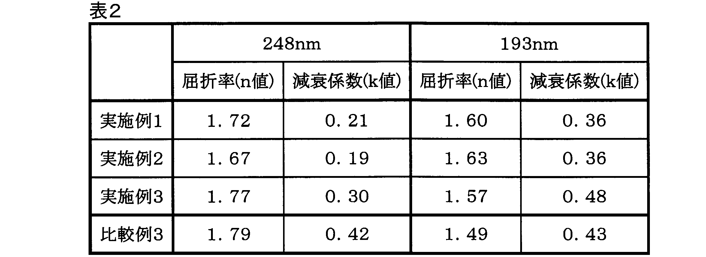
実施例1乃至実施例3、並びに比較例3で調製された各レジスト下層膜形成組成物をスピナーにより、半導体基板(シリコンウェハー)上に塗布した。その後、実施例1及び比較例3は185℃、実施例2は130℃、実施例3は195℃のホットプレート上で1分間ベークし、レジスト下層膜(膜厚0.05μm)を形成した。そして、これらのレジスト下層膜を光エリプソメーター(J.A.Woollam社製、VUV-VASE VU-302)を用い、波長248nm及び193nmでの屈折率(n値)及び減衰係数(k値)を測定した。評価の結果を下記表2に示す。
〔パターン形状の評価〕
実施例1及び実施例3、並びに比較例3で調製された各レジスト下層膜形成組成物をスピナーにより、半導体基板(シリコンウェハー)上に塗布した。その後、実施例1は185℃、実施例3は195℃、比較例3は185℃のホットプレート上で1分間ベークし、レジスト下層膜(膜厚0.04μm)を形成した。このレジスト下層膜の上に、市販のフォトレジスト溶液(東京応化工業(株)製、商品名:TDUR-P3435LP)をスピナーにより塗布し、90℃のホットプレート上で1分間加熱してフォトレジスト膜(膜厚0.265μm)を形成した。次いで、(株)ニコン製NSR-S205Cレンズスキャニング方式ステッパー(波長248nm、NA:0.75、σ:0.85(CONVENTIONAL))を用い、現像後にフォトレジストパターンのライン幅及びそのライン間の幅が0.20μmになるよう設定されたマスクを通して、露光を行った。その後、110℃のホットプレート上で1分間“露光後加熱”を行なった。冷却後、現像液として0.26規定のテトラメチルアンモニウムヒドロキシド水溶液を用いて現像した。
実施例1及び実施例3、並びに比較例3で調製された各レジスト下層膜形成組成物をスピナーにより、半導体基板(シリコンウェハー)上に塗布した。その後、実施例1は185℃、実施例3は195℃、比較例3は185℃のホットプレート上で1分間ベークし、レジスト下層膜(膜厚0.04μm)を形成した。このレジスト下層膜の上に、市販のフォトレジスト溶液(東京応化工業(株)製、商品名:TDUR-P3435LP)をスピナーにより塗布し、90℃のホットプレート上で1分間加熱してフォトレジスト膜(膜厚0.265μm)を形成した。次いで、(株)ニコン製NSR-S205Cレンズスキャニング方式ステッパー(波長248nm、NA:0.75、σ:0.85(CONVENTIONAL))を用い、現像後にフォトレジストパターンのライン幅及びそのライン間の幅が0.20μmになるよう設定されたマスクを通して、露光を行った。その後、110℃のホットプレート上で1分間“露光後加熱”を行なった。冷却後、現像液として0.26規定のテトラメチルアンモニウムヒドロキシド水溶液を用いて現像した。
現像後、得られた各フォトレジストパターンの、基板と垂直方向の断面を走査型電子顕微鏡(SEM)で観察した。得られた断面SEM像を図1(実施例1)、図2(実施例3)及び図3(比較例3)に示す。その結果、実施例1及び実施例3で調製されたレジスト下層膜形成組成物を用いた場合、得られたフォトレジストパターンの断面形状は、図1及び図2に示すように概略矩形状であった。一方、比較例3で調製されたレジスト下層膜形成組成物を用いた場合、得られたフォトレジストパターンの断面形状はレジスト下層膜との界面近傍において瘤状となり、図3に示すように矩形状とはならなかった。
Claims (5)
- 下記式(1):

ブロックイソシアネート基、メチロール基及び炭素原子数1乃至5のアルコキシメチル基からなる群から選択される置換基を少なくとも2つ有する化合物、
及び溶剤を含む、非感光性レジスト下層膜形成組成物。 - 前記ポリマーは、下記式(2):

- 前記置換基を少なくとも2つ有する化合物は前記ポリマーに対して1質量%乃至40質量%含まれる、請求項1又は請求項2に記載の非感光性レジスト下層膜形成組成物。
- 架橋触媒をさらに含む、請求項1乃至請求項3のいずれか一項に記載の非感光性レジスト下層膜形成組成物。
- さらに界面活性剤を含む、請求項1乃至請求項4のいずれか一項に記載の非感光性レジスト下層膜形成組成物。
Applications Claiming Priority (2)
| Application Number | Priority Date | Filing Date | Title |
|---|---|---|---|
| JP2011-022822 | 2011-02-04 | ||
| JP2011022822A JP2014074730A (ja) | 2011-02-04 | 2011-02-04 | 非感光性レジスト下層膜形成組成物 |
Publications (1)
| Publication Number | Publication Date |
|---|---|
| WO2012105648A1 true WO2012105648A1 (ja) | 2012-08-09 |
Family
ID=46602853
Family Applications (1)
| Application Number | Title | Priority Date | Filing Date |
|---|---|---|---|
| PCT/JP2012/052397 Ceased WO2012105648A1 (ja) | 2011-02-04 | 2012-02-02 | 非感光性レジスト下層膜形成組成物 |
Country Status (3)
| Country | Link |
|---|---|
| JP (1) | JP2014074730A (ja) |
| TW (1) | TW201248331A (ja) |
| WO (1) | WO2012105648A1 (ja) |
Cited By (4)
| Publication number | Priority date | Publication date | Assignee | Title |
|---|---|---|---|---|
| US20160349617A1 (en) * | 2015-05-29 | 2016-12-01 | Tokyo Ohka Kogyo Co., Ltd. | Method of forming resist pattern |
| US10429740B2 (en) | 2015-03-19 | 2019-10-01 | Tokyo Ohka Kogyo Co., Ltd. | Method of recovering resist pattern |
| US20200348595A1 (en) * | 2018-01-23 | 2020-11-05 | Jsr Corporation | Composition, film, and production method of patterned substrate |
| WO2020235427A1 (ja) * | 2019-05-22 | 2020-11-26 | 日産化学株式会社 | レジスト下層膜形成組成物 |
Families Citing this family (5)
| Publication number | Priority date | Publication date | Assignee | Title |
|---|---|---|---|---|
| JP6601628B2 (ja) * | 2014-05-22 | 2019-11-06 | 日産化学株式会社 | ブロックイソシアネート構造を含むポリマーを含むリソグラフィー用レジスト下層膜形成組成物 |
| JPWO2015178236A1 (ja) | 2014-05-22 | 2017-04-20 | 日産化学工業株式会社 | アクリルアミド構造とアクリル酸エステル構造を含むポリマーを含むリソグラフィー用レジスト下層膜形成組成物 |
| US10203602B2 (en) * | 2016-09-30 | 2019-02-12 | Rohm And Haas Electronic Materials Korea Ltd. | Coating compositions for use with an overcoated photoresist |
| JP7227558B2 (ja) * | 2019-02-07 | 2023-02-22 | 日油株式会社 | バインダー樹脂および導電性ペースト組成物 |
| WO2026083948A1 (ja) * | 2024-10-16 | 2026-04-23 | Jsr株式会社 | 窒素含有膜形成用組成物及び半導体基板の製造方法 |
Citations (4)
| Publication number | Priority date | Publication date | Assignee | Title |
|---|---|---|---|---|
| JPH10186671A (ja) * | 1996-12-24 | 1998-07-14 | Fuji Photo Film Co Ltd | 反射防止膜材料用組成物 |
| JP2001502439A (ja) * | 1996-09-30 | 2001-02-20 | クラリアント・インターナショナル・リミテッド | フォトレジスト組成物のための反射防止膜 |
| JP2001505234A (ja) * | 1996-08-16 | 2001-04-17 | クラリアント・インターナショナル・リミテッド | フォトレジスト組成物のための反射防止膜 |
| WO2005111724A1 (ja) * | 2004-05-14 | 2005-11-24 | Nissan Chemical Industries, Ltd. | ビニルエーテル化合物を含む反射防止膜形成組成物 |
-
2011
- 2011-02-04 JP JP2011022822A patent/JP2014074730A/ja not_active Withdrawn
-
2012
- 2012-02-02 WO PCT/JP2012/052397 patent/WO2012105648A1/ja not_active Ceased
- 2012-02-04 TW TW101103673A patent/TW201248331A/zh unknown
Patent Citations (4)
| Publication number | Priority date | Publication date | Assignee | Title |
|---|---|---|---|---|
| JP2001505234A (ja) * | 1996-08-16 | 2001-04-17 | クラリアント・インターナショナル・リミテッド | フォトレジスト組成物のための反射防止膜 |
| JP2001502439A (ja) * | 1996-09-30 | 2001-02-20 | クラリアント・インターナショナル・リミテッド | フォトレジスト組成物のための反射防止膜 |
| JPH10186671A (ja) * | 1996-12-24 | 1998-07-14 | Fuji Photo Film Co Ltd | 反射防止膜材料用組成物 |
| WO2005111724A1 (ja) * | 2004-05-14 | 2005-11-24 | Nissan Chemical Industries, Ltd. | ビニルエーテル化合物を含む反射防止膜形成組成物 |
Cited By (7)
| Publication number | Priority date | Publication date | Assignee | Title |
|---|---|---|---|---|
| US10429740B2 (en) | 2015-03-19 | 2019-10-01 | Tokyo Ohka Kogyo Co., Ltd. | Method of recovering resist pattern |
| US20160349617A1 (en) * | 2015-05-29 | 2016-12-01 | Tokyo Ohka Kogyo Co., Ltd. | Method of forming resist pattern |
| US9846364B2 (en) * | 2015-05-29 | 2017-12-19 | Tokyo Ohka Kogyo Co., Ltd. | Method of forming resist pattern |
| US20200348595A1 (en) * | 2018-01-23 | 2020-11-05 | Jsr Corporation | Composition, film, and production method of patterned substrate |
| WO2020235427A1 (ja) * | 2019-05-22 | 2020-11-26 | 日産化学株式会社 | レジスト下層膜形成組成物 |
| JPWO2020235427A1 (ja) * | 2019-05-22 | 2020-11-26 | ||
| JP7416062B2 (ja) | 2019-05-22 | 2024-01-17 | 日産化学株式会社 | レジスト下層膜形成組成物 |
Also Published As
| Publication number | Publication date |
|---|---|
| JP2014074730A (ja) | 2014-04-24 |
| TW201248331A (en) | 2012-12-01 |
Similar Documents
| Publication | Publication Date | Title |
|---|---|---|
| JP6493695B2 (ja) | レジスト下層膜形成組成物及びそれを用いたレジストパターンの形成方法 | |
| US8962234B2 (en) | Resist underlayer film forming composition and method for forming resist pattern using the same | |
| TWI681005B (zh) | 阻劑下層膜形成組成物用添加劑及含該添加劑之阻劑下層膜形成組成物 | |
| WO2012105648A1 (ja) | 非感光性レジスト下層膜形成組成物 | |
| US9448480B2 (en) | Resist underlayer film formation composition and method for forming resist pattern using the same | |
| JP7268684B2 (ja) | レジスト下層膜形成組成物及びそれを用いたレジストパターンの形成方法 | |
| KR102537120B1 (ko) | 레지스트 하층막 형성 조성물 | |
| WO2018203464A1 (ja) | 過酸化水素水溶液に対する保護膜形成組成物 | |
| JP6274445B2 (ja) | レジスト下層膜形成組成物 | |
| WO2014171326A1 (ja) | レジスト下層膜形成組成物 | |
| WO2012081619A1 (ja) | レジスト下層膜形成組成物及びそれを用いたレジストパターンの形成方法 | |
| WO2017154600A1 (ja) | レジスト下層膜形成組成物及びそれを用いたレジストパターンの形成方法 | |
| JP4697464B2 (ja) | 含窒素芳香環構造を含むリソグラフィー用反射防止膜形成組成物 | |
| JP2015145944A (ja) | レジスト下層膜形成組成物及びそれを用いたレジストパターンの形成方法 | |
| CN101065708B (zh) | 使用了两层型防反射膜的光致抗蚀剂图形的形成方法 | |
| WO2019039355A1 (ja) | レジスト下層膜形成組成物 |
Legal Events
| Date | Code | Title | Description |
|---|---|---|---|
| 121 | Ep: the epo has been informed by wipo that ep was designated in this application |
Ref document number: 12741822 Country of ref document: EP Kind code of ref document: A1 |
|
| NENP | Non-entry into the national phase |
Ref country code: DE |
|
| 122 | Ep: pct application non-entry in european phase |
Ref document number: 12741822 Country of ref document: EP Kind code of ref document: A1 |
|
| NENP | Non-entry into the national phase |
Ref country code: JP |