WO2012105168A1 - 光束制御部材および照明装置 - Google Patents
光束制御部材および照明装置 Download PDFInfo
- Publication number
- WO2012105168A1 WO2012105168A1 PCT/JP2012/000238 JP2012000238W WO2012105168A1 WO 2012105168 A1 WO2012105168 A1 WO 2012105168A1 JP 2012000238 W JP2012000238 W JP 2012000238W WO 2012105168 A1 WO2012105168 A1 WO 2012105168A1
- Authority
- WO
- WIPO (PCT)
- Prior art keywords
- lens
- light
- flux controlling
- controlling member
- light flux
- Prior art date
- Legal status (The legal status is an assumption and is not a legal conclusion. Google has not performed a legal analysis and makes no representation as to the accuracy of the status listed.)
- Ceased
Links
Images






Classifications
-
- F—MECHANICAL ENGINEERING; LIGHTING; HEATING; WEAPONS; BLASTING
- F21—LIGHTING
- F21V—FUNCTIONAL FEATURES OR DETAILS OF LIGHTING DEVICES OR SYSTEMS THEREOF; STRUCTURAL COMBINATIONS OF LIGHTING DEVICES WITH OTHER ARTICLES, NOT OTHERWISE PROVIDED FOR
- F21V5/00—Refractors for light sources
- F21V5/008—Combination of two or more successive refractors along an optical axis
-
- F—MECHANICAL ENGINEERING; LIGHTING; HEATING; WEAPONS; BLASTING
- F21—LIGHTING
- F21K—NON-ELECTRIC LIGHT SOURCES USING LUMINESCENCE; LIGHT SOURCES USING ELECTROCHEMILUMINESCENCE; LIGHT SOURCES USING CHARGES OF COMBUSTIBLE MATERIAL; LIGHT SOURCES USING SEMICONDUCTOR DEVICES AS LIGHT-GENERATING ELEMENTS; LIGHT SOURCES NOT OTHERWISE PROVIDED FOR
- F21K9/00—Light sources using semiconductor devices as light-generating elements, e.g. using light-emitting diodes [LED] or lasers
- F21K9/20—Light sources comprising attachment means
- F21K9/23—Retrofit light sources for lighting devices with a single fitting for each light source, e.g. for substitution of incandescent lamps with bayonet or threaded fittings
- F21K9/232—Retrofit light sources for lighting devices with a single fitting for each light source, e.g. for substitution of incandescent lamps with bayonet or threaded fittings specially adapted for generating an essentially omnidirectional light distribution, e.g. with a glass bulb
-
- F—MECHANICAL ENGINEERING; LIGHTING; HEATING; WEAPONS; BLASTING
- F21—LIGHTING
- F21K—NON-ELECTRIC LIGHT SOURCES USING LUMINESCENCE; LIGHT SOURCES USING ELECTROCHEMILUMINESCENCE; LIGHT SOURCES USING CHARGES OF COMBUSTIBLE MATERIAL; LIGHT SOURCES USING SEMICONDUCTOR DEVICES AS LIGHT-GENERATING ELEMENTS; LIGHT SOURCES NOT OTHERWISE PROVIDED FOR
- F21K9/00—Light sources using semiconductor devices as light-generating elements, e.g. using light-emitting diodes [LED] or lasers
- F21K9/60—Optical arrangements integrated in the light source, e.g. for improving the colour rendering index or the light extraction
-
- F—MECHANICAL ENGINEERING; LIGHTING; HEATING; WEAPONS; BLASTING
- F21—LIGHTING
- F21V—FUNCTIONAL FEATURES OR DETAILS OF LIGHTING DEVICES OR SYSTEMS THEREOF; STRUCTURAL COMBINATIONS OF LIGHTING DEVICES WITH OTHER ARTICLES, NOT OTHERWISE PROVIDED FOR
- F21V5/00—Refractors for light sources
- F21V5/04—Refractors for light sources of lens shape
-
- F—MECHANICAL ENGINEERING; LIGHTING; HEATING; WEAPONS; BLASTING
- F21—LIGHTING
- F21V—FUNCTIONAL FEATURES OR DETAILS OF LIGHTING DEVICES OR SYSTEMS THEREOF; STRUCTURAL COMBINATIONS OF LIGHTING DEVICES WITH OTHER ARTICLES, NOT OTHERWISE PROVIDED FOR
- F21V3/00—Globes; Bowls; Cover glasses
-
- F—MECHANICAL ENGINEERING; LIGHTING; HEATING; WEAPONS; BLASTING
- F21—LIGHTING
- F21V—FUNCTIONAL FEATURES OR DETAILS OF LIGHTING DEVICES OR SYSTEMS THEREOF; STRUCTURAL COMBINATIONS OF LIGHTING DEVICES WITH OTHER ARTICLES, NOT OTHERWISE PROVIDED FOR
- F21V7/00—Reflectors for light sources
- F21V7/0091—Reflectors for light sources using total internal reflection
-
- F—MECHANICAL ENGINEERING; LIGHTING; HEATING; WEAPONS; BLASTING
- F21—LIGHTING
- F21Y—INDEXING SCHEME ASSOCIATED WITH SUBCLASSES F21K, F21L, F21S and F21V, RELATING TO THE FORM OR THE KIND OF THE LIGHT SOURCES OR OF THE COLOUR OF THE LIGHT EMITTED
- F21Y2115/00—Light-generating elements of semiconductor light sources
- F21Y2115/10—Light-emitting diodes [LED]
Definitions
- the present invention relates to a light flux controlling member that controls light distribution of light emitted from a light emitting element, and an illumination device having the light flux controlling member.
- incandescent bulbs generate a wide range of uniform light from the filament by supplying power to the filament from an external power source.
- incandescent bulbs have drawbacks such as high power consumption, high temperature, and short service life.
- LED light-emitting diode
- the substrate is formed in a cylindrical shape, and the side surface of the cylinder (surface parallel to the axis of the LED bulb) and the upper surface of the cylinder (perpendicular to the axis of the LED bulb).
- LED bulbs with a wide illumination angle are disclosed, in which LEDs are mounted on both sides, and the emitted light from the LEDs is diffused by the phosphor layer formed on the inner surface of the translucent cover and emitted to the outside of the LED bulb. has been.
- the conventional LED bulb described in Patent Document 1 has a complicated structure such as the shape of the substrate and the arrangement of the LEDs, and thus the manufacturing cost is increased.
- An object of the present invention is to provide a light flux control member capable of spreading light emitted from an LED over a wide range, and a lighting device such as an LED bulb having a simple structure and a wide illumination angle. That is.
- the light flux controlling member of the present invention is a light flux controlling member for controlling the light distribution of the light emitted from the light emitting element, and has a plate-like first lens and a plate-like second lens, and the first lens Has a first surface that is one main surface, a first back surface that is the other main surface, and a first side surface that forms a planar outline of the first lens, and the second lens A second surface that is a main surface, a second back surface that is the other main surface, and a second side surface that forms a planar outer shape of the second lens, and the first lens and the second lens are The first surface and the second back surface face each other, and a low refractive index layer having a refractive index lower than that of the first lens and the second lens exists between the first surface and the second back surface.
- the first lens is formed by denting the first back surface of the first lens.
- the first lens has a first concave surface that generates light that enters the light emitted from the light emitting element and guides the light toward the first side surface
- the second lens has a concave surface on the second surface of the second lens.
- a configuration is adopted that has a second concave surface that is formed by bending and emits or totally reflects light that has entered through the first concave surface and transmitted through the first front surface and the second back surface.
- the illuminating device of the present invention employs a configuration including a light emitting element and the light flux controlling member that controls the light distribution of the light emitted from the light emitting element.
- a lighting device such as an LED bulb having a wide illumination angle with a simple structure of one LED and a lens (light flux controlling member), which can spread light emitted from the LED over a wide range. it can.
- FIG. 2A is a plan view of a light flux controlling member according to an embodiment of the present invention
- FIG. 2B is a front sectional view of the light flux controlling member
- FIG. 2C is a bottom view of the light flux controlling member
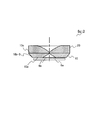
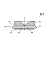
- 3A is a plan view of a light flux controlling member according to an embodiment of the present invention
- FIG. 3B is a front sectional view of the light flux controlling member
- FIG. 3C is a bottom view of the light flux controlling member.
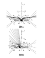
- FIG. 4A is a diagram illustrating a path of light emitted from the center of the light emitting surface of the LED and incident on the light flux controlling member according to the embodiment of the present invention, and FIG. 4B is released from the center of the light emitting surface of the LED. It is a figure which shows the path
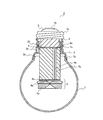
- FIG. 1 is a diagram showing an LED bulb 1 using a light flux controlling member according to an embodiment of the present invention.
- the LED bulb 1 is mainly composed of a cover 2, a base 3, a power supply unit 4, a pedestal 5, and an LED unit 6.
- the cover 2 is made of a metal having high thermal conductivity (for example, aluminum).
- the cover 2 is formed with a cylindrical base attaching portion 2a.
- a disc-like support member 2b having a hole 2c at the center is attached to the inner surface side of the base attachment portion 2a by an adhesive or the like, and the power supply unit 4 is disposed on the inner surface side of the support member 2b.
- the base 3 is made of a metal shell portion 3a formed in a cylindrical shape with a thread, and a metal portion provided on the top of one end side of the shell portion 3a with respect to the shell portion 3a via an insulating portion. It has an eyelet part 3b.
- the base 3 is fixed to the cover 2 by mounting the opening 3c which is the other end side of the shell part 3a to the base attaching part 2a of the cover 2 via an insulator.
- the power supply unit 4 has a substantially cylindrical shape, is connected to the inner side surfaces of the shell portion 3a and the eyelet portion 3b via an input electric wire (not shown), and receives power supply from the base 3. Moreover, the power supply unit 4 supplies electric power to the LED unit 6 via the output electric wire 4a.
- the pedestal 5 has a substantially cylindrical shape and is attached to the inner surface of the cover 2 with a heat conductive adhesive. Near the center of the pedestal 5, a through-hole 5 a that penetrates the pedestal 5 in the thickness direction is provided.
- the output electric wire 4 a connected to the power supply unit 4 is connected to the substrate 6 a of the LED unit 6 through the hole 2 c of the support member 2 b and the through hole 5 a of the base 5.
- the LED unit 6 includes a substrate 6a, an LED 6b, and a light flux controlling member 6c.
- the LED unit 6 is attached to the base 5 by bonding the back surface of the substrate 6 a to the base 5.
- the substrate 6a is made of a metal (for example, aluminum) having high thermal conductivity.
- An LED 6b that emits visible light is mounted on the surface of the substrate 6a.
- the LED 6b is connected to a wiring pattern (not shown) made of a copper foil formed on the surface of the substrate 6a via an insulating layer.
- the light flux controlling member 6c is attached to the substrate 6a so as to face the LED 6b, and controls the traveling direction of the light emitted from the LED 6b. Details of the shape and the like of the light flux controlling member 6c will be described later.
- the shell portion 3a and the eyelet portion 3b of the base 3 come into contact with the electrodes in the socket, and power from a commercial power source (not shown) is supplied to the power supply unit 4. Supplied.
- the power supply unit 4 supplies, for example, 160 mA of direct current power to the LED 6b on the substrate 6a via the output wire 4a.
- the LED 6b emits light when power is supplied. The light emitted from the LED 6b is emitted while the traveling direction is controlled by the light flux controlling member 6c.
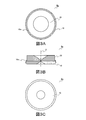
- FIG. 2A to 2C are views showing the light flux controlling member 6c according to the present embodiment.
- 2A is a plan view of the light flux controlling member 6c
- FIG. 2B is a front sectional view of the light flux controlling member 6c
- FIG. 2C is a bottom view of the light flux controlling member 6c.
- the light flux controlling member 6 c according to the present embodiment is mainly composed of a plate-like first lens 10 and a plate-like second lens 20.
- Each of the first lens 10 and the second lens 20 is, for example, a transparent resin material such as PMMA (polymethyl methacrylate), PC (polycarbonate), EP (epoxy resin), COP (cycloolefin resin), or transparent glass. Formed with.
- the first lens 10 and the second lens 20 may be made of different materials.
- the first lens 10 is formed in a thin cylindrical shape, and includes a first back surface 10a that is one main surface, a first side surface 10b that forms a planar outline of the first lens 10, and a first surface 10c that is the other main surface. And have.
- the first back surface 10a and the first surface 10c are circular planes, and the first side surface 10b is a convex curved circumferential surface.
- the first back surface 10a is recessed to form a first concave surface 10d having a conical shape with the central axis C as an apex.
- the first concave surface 10d generates light that enters the light emitted from the LED 6b and guides the light toward the first side surface 10b.
- the second lens 20 is formed in a thin cylindrical shape, and includes a second back surface 20a that is one main surface, a second side surface 20b that forms a planar outline of the second lens 20, and a second surface 20c that is the other main surface. And have.
- the second back surface 20a and the second surface 20c are circular planes, and the second side surface 20b is a circumferential curved surface having a constant diameter.
- the second surface 20c is recessed to form a curved second concave surface 20d having a curvature on the central axis C as an apex, and the curvature becomes gentler as the distance from the central axis increases.
- the second concave surface 20d emits or totally reflects light incident from the first concave surface 10d and transmitted through the first front surface 10c and the second back surface 20a.
- the first lens 10 and the second lens 20 are assembled in a state where the first surface 10c and the second back surface 20a are in contact with each other, or in a state where a minute gap exists between the first surface 10c and the second back surface 20a. It is done. In any case, the first lens 10 and the second lens 20 are not in close contact with each other, and an air layer exists between the first surface 10c and the second back surface 20a.
- the air layer functions as a low refractive index layer having a lower refractive index than the first lens 10 and the second lens 20.
- an annular convex edge portion 10e having an inner diameter substantially equal to the outer shape of the second lens 20 is formed on the outer peripheral portion of the first surface 10c of the first lens 10.
- first lens 10 and the second lens 20 can be assembled.
- a plurality of protrusions having a flat upper surface are provided on the second back surface 20a of the second lens 20, and the upper surface of each protrusion is bonded to the first surface 10c of the first lens 10 with an adhesive, thereby the first lens 10 and The second lens 20 can be assembled.
- the concave / convex fitting portion and the adhesion portion are designed so as not to have a great influence on the optical characteristics of the light flux controlling member 6c.
- the light flux controlling member 6c in which the first lens 10 and the second lens 20 are assembled is a substrate so that the first back surface 10a faces the LED 6b and the central axis C of the light flux controlling member 6c coincides with the optical axis L of the LED 6b. It is attached to 6a.
- the optical axis L is a virtual light beam that is representative of the light beam, and is emitted from the center of the light emitting surface of the LED 6b perpendicularly to the light emitting surface, and is the center of the three-dimensional light beam emitted from the LED 6b.
- the direction of light travel.
- the light flux controlling member 6c can be attached to the substrate 6a by providing a plurality of protrusions having a flat upper surface on the first back surface 10a of the first lens 10 and bonding the upper surface of each protrusion to the substrate 6a with an adhesive. .
- the light flux controlling member 6c can be attached to the substrate 6a.
- FIG. 4 is a diagram illustrating an optical path of light incident on the light flux controlling member 6c.
- 4A is a diagram illustrating an optical path of light emitted from the center of the light emitting surface of the LED 6b
- FIG. 4B is a diagram illustrating an optical path of light emitted from a point away from the center of the light emitting surface of the LED 6b.
- the angle of the light traveling direction with respect to the optical axis L (center axis C) is defined as ⁇ .
- the LED 6b emits light radially from the light emitting surface. Most of the light emitted from the LED 6 b enters from the first concave surface 10 d of the first lens 10.
- the absolute value of the angle ⁇ in the traveling direction of the light emitted from the LED 6b is smaller than 90 °.
- the light that has reached the first surface 10c at a critical angle ⁇ or less due to the material of the first lens 10 is emitted from the first surface 10c.
- the second lens 20 is incident on the second lens 20 from the second back surface 20a.
- the light that has reached the first surface 10c at an angle larger than the critical angle ⁇ is totally reflected on the first surface 10c, and then travels while being reflected between the first back surface 10a and the first surface 10c.
- the light is emitted from one side surface 10b.
- the critical angle ⁇ is approximately 42 °.
- the first concave surface 10d be formed with an inclined surface such that the concave space tapers as it approaches the first surface 10c.
- the light incident on the second lens 20 from the second back surface 20a is The light is totally reflected by the second concave surface 20d and emitted mainly from the second side surface 20b.
- a part of the light incident from the second back surface 20a is The second light is emitted from the second surface 20c or the second concave surface 20d, and the remaining light is totally reflected by the second concave surface 20d and emitted from the second side surface 20b.
- the LED 6b emits light in a planar shape instead of a point, both the light totally reflected on the second concave surface 20d and the light refracted and emitted can be generated.
- the absolute value of the angle ⁇ in the traveling direction of a part of the light emitted from the first side surface 10b or the second side surface 20b is larger than 90 °. That is, the light flux controlling member 6c spreads and emits the light emitted from the LED 6b over a wide range.
- the amount of light emitted backward ( ⁇ 90 ° ⁇ ⁇ , + 90 ° ⁇ ⁇ ) is formed by forming a downward inclined surface (an inclined surface that approaches the first back surface 10a and approaches the optical axis L) on the first side surface 10b. Can be increased.
- FIG. 5 is a diagram showing a light distribution of a conventional LED bulb that does not use the light flux control member 6c
- FIG. 6 shows a light distribution of the LED bulb using the light flux control member 6c according to the present embodiment.
- the light flux controlling member 6c of the present embodiment includes the first lens 10 and the second lens 20, and an air layer (low refractive index layer) between the first surface 10c and the second back surface 20a.
- the first concave surface 10d and the second concave surface 20d are assembled by being assembled in an existing state. Thereby, the light flux controlling member 6c can spread the light emitted from the LED 6b over a wide range. Therefore, by using the light flux controlling member 6c, it is possible to provide an illumination device such as an LED bulb having a simple structure and a wide illumination angle.
- the case where the first lens 10 and the second lens 20 are overlapped with each other via an air layer has been described.
- the low refractive index layer is not limited to the air layer.
- the low refractive index layer is not particularly limited as long as light that is totally reflected by the first surface 10c is generated.
- the first lens 10 and the second lens 20 may be bonded with a low refractive index material having a lower refractive index than the first lens 10 and the second lens 20.
- the two lenses constituting the light flux controlling member 6c are plate-like and thin, the moldability of each lens can be improved.
- FIG. 7 is a view showing the shape of variation 1 of the light flux controlling member according to the present embodiment
- FIG. 8 is a view showing the light distribution of the LED bulb having the light flux controlling member of FIG.
- the light flux controlling member 6c-1 is shown together with the substrate 6a and the LED 6b.
- the light flux controlling member 6c shown in FIG. 7 differs from the light flux controlling member 6c shown in FIG. 2 in the shape of the second side face 20b-1 of the second lens 20.
- the light flux controlling member 6c-1 shown in FIG. The second side surface 20b-1 is formed into a tapered circumferential curved surface whose diameter increases from the second back surface 20a toward the second surface 20c.
- FIG. 9 is a view showing the shape of variation 2 of the light flux controlling member according to the present embodiment
- FIG. 10 is a view showing the light distribution of the LED bulb having the light flux controlling member of FIG.
- the light flux controlling member 6c-2 is shown together with the substrate 6a and the LED 6b.
- the light beam control member 6c shown in FIG. 9 differs from the light beam control member 6c shown in FIG. 2 in the shape of the second side surface 20b-2 of the second lens 20.
- the light beam control member 6c-2 shown in FIG. The second side surface 20b-2 is formed in a tapered circumferential curved surface whose diameter decreases from the second back surface 20a toward the second surface 20c. Accordingly, as is apparent from the comparison between FIG. 6 and FIG. 10, the rear side ( ⁇ 180 ° ⁇ ⁇ 90 ° and + 90 ° ⁇ ⁇ + 180 °) of the light flux controlling member 6c shown in FIG. The amount of light can be increased.
- FIG. 11 is a view showing the shape of variation 3 of the light flux controlling member according to the present embodiment
- FIG. 12 is a view showing the light distribution of the LED bulb having the light flux controlling member of FIG.
- the light flux controlling member 6c-3 is shown together with the substrate 6a and the LED 6b.
- the first side surface 10b-3 is formed as a tapered circumferential curved surface having a diameter that increases from the first back surface 10a toward the first surface 10c.
- the rear ( ⁇ 180 ° ⁇ ⁇ 90 ° and + 90 ° ⁇ ⁇ + 180 °) of the light flux controlling member 6c shown in FIG. The amount of light can be increased.
- an upward inclined surface a tapered circumferential curved surface whose diameter decreases toward the first surface 10c
- FIG. 13 is a view showing the shape of variation 4 of the light flux controlling member according to this embodiment
- FIG. 14 is a view showing the light distribution of the LED bulb having the light flux controlling member of FIG.
- the light flux controlling member 6c-4 is shown together with the substrate 6a and the LED 6b.
- the light beam control member 6c shown in FIG. 2 is different from the light beam control member 6c shown in FIG. 2 in the shape of the first side face 10b-4 of the first lens 10.
- the first side surface 10b-4 is formed in a tapered circumferential curved surface whose diameter decreases from the first back surface 10a toward the first surface 10c.
- the light flux controlling member 6c can adjust the amount of light in the direction of the emission angle ⁇ by appropriately changing the shapes of the first concave surface, the second concave surface, the first side surface, and the second side surface.
- Directional emission is possible.
- the surface is roughened or the scattering particles are internally scattered in order to further diffuse the light emitted from the light flux controlling member 6c or to protect the LED unit.
- the cover 2 is formed with an expanded annular glove attachment portion 2 d.
- the globe 7 is formed of a transparent resin material or transparent glass into a spherical shape with an open end 7a.
- the end portion 7a is fitted inside the globe attaching portion 2d of the cover 2 and bonded by an adhesive. Thereby, the globe 7 is fixed to the cover 2 so as to cover the LED unit 6.
- a scattering material may be included in the light flux controlling member 6c within a range that does not impair the function of the light flux controlling member 6c.
- the light flux controlling member according to the present invention can be widely used in lighting devices such as LED bulbs.
Landscapes
- Engineering & Computer Science (AREA)
- General Engineering & Computer Science (AREA)
- Physics & Mathematics (AREA)
- Microelectronics & Electronic Packaging (AREA)
- Optics & Photonics (AREA)
- Non-Portable Lighting Devices Or Systems Thereof (AREA)
- Lenses (AREA)
- Optical Elements Other Than Lenses (AREA)
Abstract
照明装置(1)は、発光素子(6b)と、第1レンズ(10)および第2レンズ(20)を含む光束制御部材(6c)とを有する。第1レンズ(10)と第2レンズ(20)とは、第1表面(10c)と第2裏面(20a)とが接する状態、あるいは、第1表面(10c)と第2裏面(20a)との間に微少な間隙が存在する状態で組み付けられる。第1裏面(10a)を凹ませることにより、中心軸(C)上を頂点とする円錐面形状の第1凹面(10d)が形成される。第2表面(20c)を凹ませることにより、中心軸(C)上を頂点として中心軸から離れるに従って曲率が緩くなる曲面形状の第2凹面(20d)が形成される。
Description
本発明は、発光素子から出射された光の配光を制御する光束制御部材、および、この光束制御部材を有する照明装置に関する。
伝統的な白熱電球は、外部電源から電力をフィラメントに供給することにより、フィラメントから広範囲の均一な光線を発生する。しかしながら、白熱電球には、消費電力が高く、高温であり、使用寿命が短い、等の欠点がある。
これに対し、発光ダイオード(LED)電球は、寿命が長く、節電でき、廃棄物による環境汚染を発生しない、等の長所があるため、白熱電球に代わり、新時代の照明設備となりつつある。ただし、LEDは前方向のみにしか光が出射されないため、従来のLED電球を天井に取り付けた場合、天井および壁面を照射する光が少なくなる。そのため、同等の直下照度が得られる白熱電球と比較して、LED電球の方が暗く感じてしまう。
この課題を解決するものとして、特許文献1の図4には、基板を円筒状に形成し、円筒の側面(LED電球の軸に平行な面)および円筒の上面(LED電球の軸に垂直な面)の両方にLEDを実装するとともに、LEDからの出射光を透光性カバーの内面に形成した蛍光体層によって拡散してLED電球の外部へ出射する、照明角度を拡げたLED電球が開示されている。
しかしながら、上記特許文献1に記載された従来のLED電球は、基板の形状やLEDの配置等、構造が複雑であるため、製造コストが高くなってしまう。
本発明の目的は、LEDから出射された光を広範囲に拡げることができる光束制御部材、および、この光束制御部材を有し、簡単な構造で照明角度が広いLED電球等の照明装置を提供することである。
本発明の光束制御部材は、発光素子から出射された光の配光を制御する光束制御部材であって、板状の第1レンズと板状の第2レンズとを有し、前記第1レンズは、一方の主面である第1表面と、他方の主面である第1裏面と、前記第1レンズの平面外形を形作る第1側面と、を有し、前記第2レンズは、一方の主面である第2表面と、他方の主面である第2裏面と、前記第2レンズの平面外形を形作る第2側面と、を有し、前記第1レンズおよび前記第2レンズは、前記第1表面と前記第2裏面とが対向し、かつ前記第1表面と前記第2裏面との間に前記第1レンズおよび前記第2レンズよりも屈折率が低い低屈折率層が存在するように重ねて配置され、前記第1レンズは、前記第1レンズの前記第1裏面を凹ませることにより形成され、前記発光素子から出射された光を入射して前記第1側面に向かって導光する光を生成する第1凹面を有し、前記第2レンズは、前記第2レンズの前記第2表面を凹ませることにより形成され、前記第1凹面から入射して前記第1表面および前記第2裏面を透過した光を出射又は全反射させる第2凹面を有する、構成を採る。
本発明の照明装置は、発光素子と、前記発光素子から出射された光の配光を制御する上記光束制御部材と、を備える構成を採る。
本発明によれば、LEDから出射された光を広範囲に拡げることができ、LED1個とレンズ(光束制御部材)という簡単な構造で、照明角度が広いLED電球等の照明装置を提供することができる。
以下、本発明の実施の形態について、図面を参照して詳細に説明する。以下の説明では、本発明の照明装置の代表例として、発光素子としてLEDを有するLED電球について説明する。
〔LED電球の構成〕
図1は、本発明の一実施の形態に係る光束制御部材を用いたLED電球1を示す図である。
図1は、本発明の一実施の形態に係る光束制御部材を用いたLED電球1を示す図である。
LED電球1は、カバー2と、口金3と、電源ユニット4と、台座5と、LEDユニット6と、から主に構成される。
カバー2は、高熱伝導性を有する金属(例えばアルミニウム)からなる。カバー2には円筒状の口金取り付け部2aが形成される。口金取り付け部2aの内面側には、中央部に孔2cを有する円盤状の支持部材2bが接着剤等によって取り付けられ、支持部材2bの内面側に電源ユニット4が配設される。
口金3は、ねじ山を備えた筒状に形成された金属製のシェル部3a、および、シェル部3aの一端側の頂部にシェル部3aに対して絶縁部を介して設けられた金属製のアイレット部3bを有する。口金3は、シェル部3aの他端側である開口3cを、絶縁物を介してカバー2の口金取り付け部2aに装着することにより、カバー2に固定される。
電源ユニット4は、略円柱形状であり、入力電線(図示せず)を介してシェル部3aとアイレット部3bの内側面に接続し、口金3から電力の供給を受ける。また、電源ユニット4は、出力電線4aを介してLEDユニット6に電力を供給する。
台座5は、略円柱形状であり、伝熱性の接着材によりカバー2の内面に取り付けられる。台座5の中央付近には、台座5を厚み方向に貫通した貫通孔5aが設けられる。電源ユニット4に接続された出力電線4aは、支持部材2bの孔2cおよび台座5の貫通孔5aを通ってLEDユニット6の基板6aに接続される。
LEDユニット6は、基板6aと、LED6bと、光束制御部材6cと、から構成される。LEDユニット6は、基板6aの裏面を台座5に接着することにより台座5に取り付けられる。基板6aは、高熱伝導性を有する金属(例えばアルミニウム)からなる。基板6aの表面には、可視光を放射するLED6bが実装される。LED6bは、基板6aの表面に絶縁層を介して形成された銅箔からなる配線パターン(図示せず)に接続される。光束制御部材6cは、LED6bに対向するように基板6aに取り付けられ、LED6bから出射された光の進行方向を制御する。なお、光束制御部材6cの形状等の詳細については後述する。
LED電球1を電球用ソケット(図示せず)に取り付けると、口金3のシェル部3aとアイレット部3bがソケット内の電極と接触し、商用電源(図示せず)からの電力が電源ユニット4に供給される。電源ユニット4は、例えば160mAの直流電流の電力を、出力電線4aを介して基板6a上のLED6bに供給する。LED6bは、電力が供給されると発光する。LED6bから出射された光は、光束制御部材6cによって進行方向を制御されて出射される。
〔光束制御部材の形状〕
図2A~Cは、本実施の形態に係る光束制御部材6cを示す図である。図2Aは光束制御部材6cの平面図、図2Bは光束制御部材6cの正面断面図、図2Cは光束制御部材6cの底面図である。図2に示すように、本実施の形態に係る光束制御部材6cは、板状の第1レンズ10と、板状の第2レンズ20と、から主に構成される。
図2A~Cは、本実施の形態に係る光束制御部材6cを示す図である。図2Aは光束制御部材6cの平面図、図2Bは光束制御部材6cの正面断面図、図2Cは光束制御部材6cの底面図である。図2に示すように、本実施の形態に係る光束制御部材6cは、板状の第1レンズ10と、板状の第2レンズ20と、から主に構成される。
第1レンズ10及び第2レンズ20は、いずれも、例えば、PMMA(ポリメタクリル酸メチル)、PC(ポリカーボネート)、EP(エポキシ樹脂)、COP(シクロオレフィン樹脂)等の透明樹脂材料や透明なガラスで形成される。なお、第1レンズ10と第2レンズ20とは、互いに材質が異なっていても良い。
第1レンズ10は、薄肉円柱形状に形成され、一方の主面である第1裏面10aと、第1レンズ10の平面外形を形作る第1側面10bと、他方の主面である第1表面10cとを有する。第1裏面10aおよび第1表面10cは円形平面であり、第1側面10bは凸プリズム形状の円周曲面である。第1裏面10aの中央部には、第1裏面10aを凹ませることにより、中心軸C上を頂点とする円錐面形状の第1凹面10dが形成される。後述するように、第1凹面10dは、LED6bから出射された光を入射して第1側面10bに向かって導光する光を生成する。
第2レンズ20は、薄肉円柱形状に形成され、一方の主面である第2裏面20aと、第2レンズ20の平面外形を形作る第2側面20bと、他方の主面である第2表面20cとを有する。第2裏面20aおよび第2表面20cは円形平面であり、第2側面20bは径が一定の円周曲面である。第2表面20cの中央部には、第2表面20cを凹ませることにより、中心軸C上を頂点として中心軸から離れるに従って曲率が緩くなる曲面形状の第2凹面20dが形成される。後述するように、第2凹面20dは、第1凹面10dから入射して第1表面10cおよび第2裏面20aを透過した光を出射又は全反射させる。
〔光束制御部材のレンズの組み付け〕
第1レンズ10と第2レンズ20とは、第1表面10cと第2裏面20aとが接する状態、あるいは、第1表面10cと第2裏面20aとの間に微少な間隙が存在する状態で組み付けられる。いずれの場合であっても、第1レンズ10と第2レンズ20とは密着しておらず、第1表面10cと第2裏面20aとの間には空気層が存在する。空気層は、第1レンズ10および第2レンズ20よりも屈折率が低い低屈折率層として機能する。
第1レンズ10と第2レンズ20とは、第1表面10cと第2裏面20aとが接する状態、あるいは、第1表面10cと第2裏面20aとの間に微少な間隙が存在する状態で組み付けられる。いずれの場合であっても、第1レンズ10と第2レンズ20とは密着しておらず、第1表面10cと第2裏面20aとの間には空気層が存在する。空気層は、第1レンズ10および第2レンズ20よりも屈折率が低い低屈折率層として機能する。
なお、本発明において、第1レンズ10と第2レンズ20の組み付け方については制限がない。
例えば、図3A~Cに示すように、第1レンズ10の第1表面10cの外周部に、内径が第2レンズ20の外形とほぼ等しい円環状の凸縁部10eを形成し、第2レンズ20を第1レンズ10の凸縁部10eに嵌合させることにより、第1レンズ10と第2レンズ20とを組み付けることができる。
あるいは、第1レンズ10の第1表面10cに微少な凹みを複数設け、第2レンズ20の第2裏面20aにこれらの凹みに対応する突起を設け、各突起を各凹みに嵌合させることにより、第1レンズ10と第2レンズ20とを組み付けることができる。
あるいは、第2レンズ20の第2裏面20aに、上面が平面の突起を複数設け、接着剤によって第1レンズ10の第1表面10cに各突起の上面を接着することにより、第1レンズ10と第2レンズ20とを組み付けることができる。
いずれの組み付け例においても、凹凸嵌合部や接着部が光束制御部材6cの光学特性に大きな影響を与えないように設計される。
〔光束制御部材の取り付け〕
第1レンズ10と第2レンズ20とが組み付けられた光束制御部材6cは、第1裏面10aがLED6bに対向し、光束制御部材6cの中心軸CがLED6bの光軸Lと一致するように基板6aに取り付けられる。
第1レンズ10と第2レンズ20とが組み付けられた光束制御部材6cは、第1裏面10aがLED6bに対向し、光束制御部材6cの中心軸CがLED6bの光軸Lと一致するように基板6aに取り付けられる。
光軸Lとは、光束の代表となる仮想的な光線であって、LED6bの発光面の中心から発光面と垂直に出射される光であって、LED6bから出射される立体的な光束の中心における光の進行方向をいう。
なお、本発明において、光束制御部材6cの基板6aへの取り付け方については制限がない。
例えば、第1レンズ10の第1裏面10aに、上面が平面の突起を複数設け、接着剤によって基板6aに各突起の上面を接着することにより、光束制御部材6cを基板6aに取り付けることができる。
あるいは、基板6aに凹み、または貫通孔を複数設け、第1レンズ10の第1裏面10aにこれらの凹みに対応する突起を設け、各突起を各凹みに嵌合させることにより、光束制御部材6cを基板6aに取り付けることができる。
〔光束制御部材内の光の経路〕
図4は、光束制御部材6cに入射する光の光路を示す図である。図4Aは、LED6bの発光面の中心から出射される光の光路を示す図であり、図4Bは、LED6bの発光面の中心より離れた点から出射される光の光路を示す図である。なお、以下の説明において、光軸L(中心軸C)に対する光の進行方向の角度をθとする。
図4は、光束制御部材6cに入射する光の光路を示す図である。図4Aは、LED6bの発光面の中心から出射される光の光路を示す図であり、図4Bは、LED6bの発光面の中心より離れた点から出射される光の光路を示す図である。なお、以下の説明において、光軸L(中心軸C)に対する光の進行方向の角度をθとする。
図4Aおよび図4Bに示すように、LED6bは発光面から放射状に光を出射する。LED6bから出射された光の大部分は、第1レンズ10の第1凹面10dから入射する。なお、LED6bから出射される光の進行方向の角度θの絶対値は90°より小さくなる。
図4Aおよび図4Bに示すように、第1凹面10dから入射した光の内、第1レンズ10の材料による臨界角φ以下で第1表面10cに到達した光は、第1表面10cから出射され、第2レンズ20の第2裏面20aから第2レンズ20内に入射する。一方、臨界角φより大きい角度で第1表面10cに到達した光は、第1表面10cにおいて全反射され、その後、第1裏面10aと第1表面10cとの間を反射しながら進行し、第1側面10bから出射される。なお、第1レンズ10の材料がアクリルの場合、臨界角φはおよそ42°である。
LED6bから出射された光が、第1凹面10dが形成されない第1裏面10aから第1レンズ10内に入射した場合には、略全光量が第1表面10cから出射することとなり、第1レンズ10内を導光する光が生成されない。したがって、第1凹面10dには、第1表面10cに近づくにしたがって凹部空間が先細りになるような傾斜面が形成されていることが必要である。
図4Aに示すように、LED6bの発光面の1点(本実施の形態においては発光面の中心)から出射された光の内、第2裏面20aから第2レンズ20内に入射した光は、第2凹面20dで全反射され、主として第2側面20bから出射される。
また、図4Bに示すように、LED6bの発光面の別の点(本実施の形態においては中心より離れた点)から出射された光の内、第2裏面20aから入射した一部の光は、第2表面20cあるいは第2凹面20dから出射され、残りの光は、第2凹面20dで全反射され、第2側面20bから出射される。このように、LED6bが点ではなく面状に発光していることにより、第2凹面20dにおいて全反射する光および屈折して出射する光の両方を生成することができる。
図4Aおよび図4Bに示すように、第1側面10bあるいは第2側面20bから出射される光の一部の進行方向の角度θの絶対値は、90°より大きくなる。すなわち、光束制御部材6cは、LED6bから出射された光を広範囲に拡げて出射する。第1側面10bに下向きの傾斜面(第1裏面10aに近づくとともに光軸Lに近づくような傾斜面)を形成することにより、後方(-90°≧θ、+90°≦θ)への出射光量を増やすことが可能となる。
〔配光分布の対比〕
図5は、光束制御部材6cを用いない従来のLED電球の配光分布を示す図であり、図6は、本実施の形態に係る光束制御部材6cを用いたLED電球の配光分布を示す図である。
図5は、光束制御部材6cを用いない従来のLED電球の配光分布を示す図であり、図6は、本実施の形態に係る光束制御部材6cを用いたLED電球の配光分布を示す図である。
図5に示すように、従来のLED電球では、前方(-90°<θ<+90°)のみにしか光が出射されていない。これに対し、本実施の形態に係る光束制御部材6cを有するLED電球では、後方(-180°<θ<-90°および+90°<θ≦+180°)にも光が出射されている。
〔本実施の形態の効果〕
以上のように、本実施の形態の光束制御部材6cは、第1レンズ10と第2レンズ20とを、第1表面10cと第2裏面20aとの間に空気層(低屈折率層)が存在する状態で組み付けて構成され、第1凹面10dおよび第2凹面20dを有する。これにより、光束制御部材6cは、LED6bから出射された光を広範囲に拡げることができる。したがって、光束制御部材6cを用いることにより、簡単な構造で照明角度が広いLED電球等の照明装置を提供することができる。なお、本実施の形態では第1レンズ10と第2レンズ20とを空気層を介して重ね合わせる場合について説明したが、低屈折率層は空気層に限定されない。低屈折率層は、第1表面10cで全反射する光が生成されるのであれば特に限定されない。例えば、第1レンズ10と第2レンズ20とを第1レンズ10および第2レンズ20よりも屈折率が低い低屈折率材料で接着してもよい。
以上のように、本実施の形態の光束制御部材6cは、第1レンズ10と第2レンズ20とを、第1表面10cと第2裏面20aとの間に空気層(低屈折率層)が存在する状態で組み付けて構成され、第1凹面10dおよび第2凹面20dを有する。これにより、光束制御部材6cは、LED6bから出射された光を広範囲に拡げることができる。したがって、光束制御部材6cを用いることにより、簡単な構造で照明角度が広いLED電球等の照明装置を提供することができる。なお、本実施の形態では第1レンズ10と第2レンズ20とを空気層を介して重ね合わせる場合について説明したが、低屈折率層は空気層に限定されない。低屈折率層は、第1表面10cで全反射する光が生成されるのであれば特に限定されない。例えば、第1レンズ10と第2レンズ20とを第1レンズ10および第2レンズ20よりも屈折率が低い低屈折率材料で接着してもよい。
さらに、本実施の形態によれば、光束制御部材6cを構成する2枚のレンズが、板状で薄肉であるので、各レンズの成形性を良くすることができる。
〔バリエーション〕
以下、本実施の形態に係る光束制御部材のバリエーションについて、図7から図14を用いて説明する。
以下、本実施の形態に係る光束制御部材のバリエーションについて、図7から図14を用いて説明する。
図7は、本実施の形態に係る光束制御部材のバリエーション1の形状を示す図であり、図8は、図7の光束制御部材を有するLED電球の配光分布を示す図である。なお、図7では、基板6aおよびLED6bとともに光束制御部材6c-1を示す。
図7に示す光束制御部材6c-1は、図2に示した光束制御部材6cと比較して、第2レンズ20の第2側面20b-1の形状が異なる。第2側面20b-1は、第2裏面20aから第2表面20cに向かって径が大きくなるテーパー形状の円周曲面に形成される。これにより、図6と図8との対比から明らかなように、図2に示した光束制御部材6cよりも、前方(-90°<θ<+90°)の光量を増やすことができる。
図9は、本実施の形態に係る光束制御部材のバリエーション2の形状を示す図であり、図10は、図9の光束制御部材を有するLED電球の配光分布を示す図である。なお、図9では、基板6aおよびLED6bとともに光束制御部材6c-2を示す。
図9に示す光束制御部材6c-2は、図2に示した光束制御部材6cと比較して、第2レンズ20の第2側面20b-2の形状が異なる。第2側面20b-2は、第2裏面20aから第2表面20cに向かって径が小さくなるテーパー形状の円周曲面に形成される。これにより、図6と図10との対比から明らかなように、図2に示した光束制御部材6cよりも、後方(-180°<θ<-90°および+90°<θ≦+180°)の光量を増やすことができる。
図11は、本実施の形態に係る光束制御部材のバリエーション3の形状を示す図であり、図12は、図11の光束制御部材を有するLED電球の配光分布を示す図である。なお、図11では、基板6aおよびLED6bとともに光束制御部材6c-3を示す。
図11に示す光束制御部材6c-3は、図2に示した光束制御部材6cと比較して、第1レンズ10の第1側面10b-3の形状が異なる。第1側面10b-3は、第1裏面10aから第1表面10cに向かって径が大きくなるテーパー形状の円周曲面に形成される。これにより、図6と図12との対比から明らかなように、図2に示した光束制御部材6cよりも、後方(-180°<θ<-90°および+90°<θ≦+180°)の光量を増やすことができる。上向きの傾斜面(第1表面10cに向かって径が小さくなるテーパー形状の円周曲面)が形成されていないため、上向きの傾斜面が形成されている図2に示した光束制御部材6cと比較して、前方(-90°<θ<+90°)への出射光量は減少している。
図13は、本実施の形態に係る光束制御部材のバリエーション4の形状を示す図であり、図14は、図13の光束制御部材を有するLED電球の配光分布を示す図である。なお、図13では、基板6aおよびLED6bとともに光束制御部材6c-4を示す。
図13に示す光束制御部材6c-4は、図2に示した光束制御部材6cと比較して、第1レンズ10の第1側面10b-4の形状が異なる。第1側面10b-4は、第1裏面10aから第1表面10cに向かって径が小さくなるテーパー形状の円周曲面に形成される。これにより、図6と図14との対比から明らかなように、図2に示した光束制御部材6cよりも、前方(-90°<θ<+90°)の光量を増やすことができる。また、第1裏面10aの面積が基板6aの面積よりも大きく、第1裏面10aからも光を出射させることができるため、θ=180°方向への光量を増やすこともできる。
本発明に係る光束制御部材6cは、第1凹面、第2凹面、第1側面、第2側面の形状を適宜変更することにより、出射角度θ方向への光量を調整することが可能となり、全方位出射が可能となる。
本発明に係る照明装置には、光束制御部材6cからの出射光を更に拡散させるため、またはLEDユニットの保護のために、図15に示すように、表面が粗面化されたり内部に散乱粒子等が混入されたりしたグローブ7を取り付けてもよい。図15において、カバー2には拡開した環状のグローブ取り付け部2dが形成される。グローブ7は、透明樹脂材料または透明なガラスによって、端部7aが開口する球面状に形成される。端部7aがカバー2のグローブ取り付け部2dの内側に嵌合され、接着剤によって接着される。これにより、グローブ7は、LEDユニット6を覆うように、カバー2に固定される。
また、光束制御部材6cの機能を損なわない範囲で、光束制御部材6c内に散乱材が含まれていてもよい。
本出願は、2011年2月3日出願の特願2011-021586に基づく優先権を主張する。当該出願明細書および図面に記載された内容は、すべて本願明細書に援用される。
本発明に係る光束制御部材は、LED電球等の照明装置に広く活用することができる。
1 LED電球
2 カバー
3 口金
4 電源ユニット
5 台座
6 LEDユニット
6a 基板
6b LED
6c 光束制御部材
7 グローブ
10 第1レンズ
10a 第1裏面
10b 第1側面
10c 第1表面
10d 第1凹面
10e 凸縁部
20 第2レンズ
20a 第2裏面
20b 第2側面
20c 第2表面
20d 第2凹面
2 カバー
3 口金
4 電源ユニット
5 台座
6 LEDユニット
6a 基板
6b LED
6c 光束制御部材
7 グローブ
10 第1レンズ
10a 第1裏面
10b 第1側面
10c 第1表面
10d 第1凹面
10e 凸縁部
20 第2レンズ
20a 第2裏面
20b 第2側面
20c 第2表面
20d 第2凹面
Claims (9)
- 発光素子から出射された光の配光を制御する光束制御部材であって、
板状の第1レンズと板状の第2レンズとを有し、
前記第1レンズは、一方の主面である第1表面と、他方の主面である第1裏面と、前記第1レンズの平面外形を形作る第1側面と、を有し、
前記第2レンズは、一方の主面である第2表面と、他方の主面である第2裏面と、前記第2レンズの平面外形を形作る第2側面と、を有し、
前記第1レンズおよび前記第2レンズは、前記第1表面と前記第2裏面とが対向し、かつ前記第1表面と前記第2裏面との間に前記第1レンズおよび前記第2レンズよりも屈折率が低い低屈折率層が存在するように重ねて配置され、
前記第1レンズは、前記第1レンズの前記第1裏面を凹ませることにより形成され、前記発光素子から出射された光を入射して前記第1側面に向かって導光する光を生成する第1凹面を有し、
前記第2レンズは、前記第2レンズの前記第2表面を凹ませることにより形成され、前記第1凹面から入射して前記第1表面および前記第2裏面を透過した光を出射又は全反射させる第2凹面を有する、
光束制御部材。 - 前記第1凹面は、前記第1レンズの中心軸上を頂点とする円錐面形状である、請求項1に記載の光束制御部材。
- 前記第2凹面は、前記第2レンズの中心軸上を頂点として中心軸から離れるに従って曲率が緩くなる曲面形状である、請求項1に記載の光束制御部材。
- 前記第1レンズの側面は、凸プリズム形状の円周曲面を有する、請求項1に記載の光束制御部材。
- 前記第1レンズの側面は、前記第1裏面から前記第1表面に向かって径が大きくなるテーパー形状の円周曲面を有する、請求項1に記載の光束制御部材。
- 前記第1レンズの側面は、前記第1裏面から前記第1表面に向かって径が小さくなるテーパー形状の円周曲面を有する、請求項1に記載の光束制御部材。
- 前記第2レンズの側面は、前記第2裏面から前記第2表面に向かって径が大きくなるテーパー形状の円周曲面を有する、請求項1に記載の光束制御部材。
- 前記第2レンズの側面は、前記第2裏面から前記第2表面に向かって径が小さくなるテーパー形状の円周曲面を有する、請求項1に記載の光束制御部材。
- 発光素子と、
前記発光素子から出射された光の配光を制御する請求項1に記載の光束制御部材と、
を備える照明装置。
Priority Applications (2)
| Application Number | Priority Date | Filing Date | Title |
|---|---|---|---|
| US13/983,096 US8979317B2 (en) | 2011-02-03 | 2012-01-17 | Luminous flux control member and illumination device |
| CN201280007045.0A CN103339435B (zh) | 2011-02-03 | 2012-01-17 | 光束控制部件及照明装置 |
Applications Claiming Priority (2)
| Application Number | Priority Date | Filing Date | Title |
|---|---|---|---|
| JP2011021586A JP5643670B2 (ja) | 2011-02-03 | 2011-02-03 | 光束制御部材および照明装置 |
| JP2011-021586 | 2011-02-03 |
Publications (1)
| Publication Number | Publication Date |
|---|---|
| WO2012105168A1 true WO2012105168A1 (ja) | 2012-08-09 |
Family
ID=46602398
Family Applications (1)
| Application Number | Title | Priority Date | Filing Date |
|---|---|---|---|
| PCT/JP2012/000238 Ceased WO2012105168A1 (ja) | 2011-02-03 | 2012-01-17 | 光束制御部材および照明装置 |
Country Status (4)
| Country | Link |
|---|---|
| US (1) | US8979317B2 (ja) |
| JP (1) | JP5643670B2 (ja) |
| CN (1) | CN103339435B (ja) |
| WO (1) | WO2012105168A1 (ja) |
Cited By (2)
| Publication number | Priority date | Publication date | Assignee | Title |
|---|---|---|---|---|
| JP2015099205A (ja) * | 2013-11-18 | 2015-05-28 | パナソニックIpマネジメント株式会社 | 照明器具用配光レンズ及び照明器具 |
| US20150241028A1 (en) * | 2012-09-11 | 2015-08-27 | Enplas Corporation | Illumination device |
Families Citing this family (10)
| Publication number | Priority date | Publication date | Assignee | Title |
|---|---|---|---|---|
| JP5621938B2 (ja) * | 2011-09-27 | 2014-11-12 | 東芝ライテック株式会社 | 照明器具 |
| JP5868106B2 (ja) * | 2011-10-06 | 2016-02-24 | 日立アプライアンス株式会社 | 照明装置 |
| CN103511977A (zh) * | 2012-06-19 | 2014-01-15 | 欧司朗股份有限公司 | 透镜和包括该透镜的全向照明装置、改型灯 |
| US8864346B2 (en) * | 2012-12-10 | 2014-10-21 | GE Lighting Solutions, LLC | Lens-reflector combination for batwing light distribution |
| JP6304938B2 (ja) * | 2013-04-26 | 2018-04-04 | 株式会社東芝 | 照明装置および広配光レンズ |
| TWI477715B (zh) * | 2013-05-31 | 2015-03-21 | Lite On Technology Corp | 照明裝置 |
| JP2013239467A (ja) * | 2013-09-05 | 2013-11-28 | Sharp Corp | 照明装置 |
| JP6310285B2 (ja) * | 2014-03-18 | 2018-04-11 | 株式会社エンプラス | 発光装置、面光源装置および表示装置 |
| JP2015035432A (ja) * | 2014-11-17 | 2015-02-19 | シャープ株式会社 | 照明装置 |
| JP6440512B2 (ja) * | 2015-02-02 | 2018-12-19 | シチズン電子株式会社 | Led照明装置 |
Citations (3)
| Publication number | Priority date | Publication date | Assignee | Title |
|---|---|---|---|---|
| JP2004133391A (ja) * | 2002-06-24 | 2004-04-30 | Lumileds Lighting Us Llc | 側面放射led及びレンズ |
| JP2006099117A (ja) * | 2004-09-24 | 2006-04-13 | Shogen Koden Kofun Yugenkoshi | 照明パッケージ |
| JP2006113556A (ja) * | 2004-10-15 | 2006-04-27 | Samsung Electro Mech Co Ltd | Led光源用レンズ |
Family Cites Families (7)
| Publication number | Priority date | Publication date | Assignee | Title |
|---|---|---|---|---|
| JP2001243807A (ja) | 2000-02-28 | 2001-09-07 | Mitsubishi Electric Lighting Corp | Led電球 |
| MXPA03008637A (es) * | 2001-03-27 | 2005-03-07 | Meridian Automotive Sys Inc | Montaje de lampara vehicular con estructura simplificada y chmsl y lampara trasera que incorpora el mismo. |
| TWI359987B (en) * | 2004-09-24 | 2012-03-11 | Epistar Corp | Liquid crystal display and light emitting unit the |
| US8070329B1 (en) * | 2005-02-11 | 2011-12-06 | Gentex Corporation | Light emitting optical systems and assemblies and systems incorporating the same |
| DE202005007500U1 (de) * | 2005-05-12 | 2005-07-21 | Zweibrüder Optoelectronics GmbH | Taschenlampe |
| CN201697041U (zh) * | 2010-06-24 | 2011-01-05 | 杭州华奕兴电子机械有限公司 | 一种led透镜 |
| US8496349B2 (en) * | 2011-01-04 | 2013-07-30 | Unity Opto Technology Co., Ltd. | Uniform light emitting lamp structure |
-
2011
- 2011-02-03 JP JP2011021586A patent/JP5643670B2/ja not_active Expired - Fee Related
-
2012
- 2012-01-17 CN CN201280007045.0A patent/CN103339435B/zh not_active Expired - Fee Related
- 2012-01-17 WO PCT/JP2012/000238 patent/WO2012105168A1/ja not_active Ceased
- 2012-01-17 US US13/983,096 patent/US8979317B2/en not_active Expired - Fee Related
Patent Citations (3)
| Publication number | Priority date | Publication date | Assignee | Title |
|---|---|---|---|---|
| JP2004133391A (ja) * | 2002-06-24 | 2004-04-30 | Lumileds Lighting Us Llc | 側面放射led及びレンズ |
| JP2006099117A (ja) * | 2004-09-24 | 2006-04-13 | Shogen Koden Kofun Yugenkoshi | 照明パッケージ |
| JP2006113556A (ja) * | 2004-10-15 | 2006-04-27 | Samsung Electro Mech Co Ltd | Led光源用レンズ |
Cited By (3)
| Publication number | Priority date | Publication date | Assignee | Title |
|---|---|---|---|---|
| US20150241028A1 (en) * | 2012-09-11 | 2015-08-27 | Enplas Corporation | Illumination device |
| US9671087B2 (en) * | 2012-09-11 | 2017-06-06 | Enplas Corporation | Illumination device |
| JP2015099205A (ja) * | 2013-11-18 | 2015-05-28 | パナソニックIpマネジメント株式会社 | 照明器具用配光レンズ及び照明器具 |
Also Published As
| Publication number | Publication date |
|---|---|
| JP2012163602A (ja) | 2012-08-30 |
| CN103339435B (zh) | 2015-12-23 |
| CN103339435A (zh) | 2013-10-02 |
| US20130314926A1 (en) | 2013-11-28 |
| JP5643670B2 (ja) | 2014-12-17 |
| US8979317B2 (en) | 2015-03-17 |
Similar Documents
| Publication | Publication Date | Title |
|---|---|---|
| JP5643670B2 (ja) | 光束制御部材および照明装置 | |
| CN102654252B (zh) | 透镜以及照明装置 | |
| CN103032729B (zh) | 照明装置 | |
| US9360191B2 (en) | Lighting device | |
| JP6549595B2 (ja) | 照明デバイス | |
| US10480721B2 (en) | Light flux controlling member, light emitting device and illuminating device | |
| JP2016046067A (ja) | 広角度拡散光学系及びこれを用いた照明装置 | |
| JP2014093298A (ja) | 発光ダイオード電球 | |
| US8956015B2 (en) | Light-emitting apparatus and lighting system | |
| JP2013200963A (ja) | 半導体光源および照明装置 | |
| JP2017050187A (ja) | 照明器具 | |
| US10190730B2 (en) | Light flux controlling member, light emitting device and illuminating device | |
| JPWO2012023602A1 (ja) | 車両用灯具 | |
| JP6188611B2 (ja) | 照明装置 | |
| JP5970210B2 (ja) | 電球形ledランプ | |
| JP5701675B2 (ja) | カバー及び当該カバーを備えた照明装置 | |
| KR101682676B1 (ko) | 산란기능이 부가된 엘이디 조명용 확산렌즈 | |
| WO2016181789A1 (ja) | 光束制御部材、発光装置および照明装置 | |
| JP6081563B2 (ja) | 照明装置 | |
| JP5860132B2 (ja) | カバー及び当該カバーを備えた照明装置 | |
| JP3183249U (ja) | Led発光装置 | |
| JP2016146260A (ja) | 照明ランプ及び照明装置 | |
| JP2014235939A (ja) | 照明ランプ及び照明装置 | |
| JP2012204219A (ja) | 照明装置およびその製造方法 | |
| JP2019145314A (ja) | 発光モジュール及び照明装置 |
Legal Events
| Date | Code | Title | Description |
|---|---|---|---|
| 121 | Ep: the epo has been informed by wipo that ep was designated in this application |
Ref document number: 12741573 Country of ref document: EP Kind code of ref document: A1 |
|
| WWE | Wipo information: entry into national phase |
Ref document number: 13983096 Country of ref document: US |
|
| NENP | Non-entry into the national phase |
Ref country code: DE |
|
| 122 | Ep: pct application non-entry in european phase |
Ref document number: 12741573 Country of ref document: EP Kind code of ref document: A1 |