WO2016181789A1 - 光束制御部材、発光装置および照明装置 - Google Patents
光束制御部材、発光装置および照明装置 Download PDFInfo
- Publication number
- WO2016181789A1 WO2016181789A1 PCT/JP2016/062666 JP2016062666W WO2016181789A1 WO 2016181789 A1 WO2016181789 A1 WO 2016181789A1 JP 2016062666 W JP2016062666 W JP 2016062666W WO 2016181789 A1 WO2016181789 A1 WO 2016181789A1
- Authority
- WO
- WIPO (PCT)
- Prior art keywords
- light
- central axis
- total reflection
- incident
- reflection surface
- Prior art date
Links
Images


Classifications
-
- F—MECHANICAL ENGINEERING; LIGHTING; HEATING; WEAPONS; BLASTING
- F21—LIGHTING
- F21V—FUNCTIONAL FEATURES OR DETAILS OF LIGHTING DEVICES OR SYSTEMS THEREOF; STRUCTURAL COMBINATIONS OF LIGHTING DEVICES WITH OTHER ARTICLES, NOT OTHERWISE PROVIDED FOR
- F21V5/00—Refractors for light sources
-
- F—MECHANICAL ENGINEERING; LIGHTING; HEATING; WEAPONS; BLASTING
- F21—LIGHTING
- F21K—NON-ELECTRIC LIGHT SOURCES USING LUMINESCENCE; LIGHT SOURCES USING ELECTROCHEMILUMINESCENCE; LIGHT SOURCES USING CHARGES OF COMBUSTIBLE MATERIAL; LIGHT SOURCES USING SEMICONDUCTOR DEVICES AS LIGHT-GENERATING ELEMENTS; LIGHT SOURCES NOT OTHERWISE PROVIDED FOR
- F21K9/00—Light sources using semiconductor devices as light-generating elements, e.g. using light-emitting diodes [LED] or lasers
- F21K9/20—Light sources comprising attachment means
- F21K9/23—Retrofit light sources for lighting devices with a single fitting for each light source, e.g. for substitution of incandescent lamps with bayonet or threaded fittings
- F21K9/232—Retrofit light sources for lighting devices with a single fitting for each light source, e.g. for substitution of incandescent lamps with bayonet or threaded fittings specially adapted for generating an essentially omnidirectional light distribution, e.g. with a glass bulb
-
- F—MECHANICAL ENGINEERING; LIGHTING; HEATING; WEAPONS; BLASTING
- F21—LIGHTING
- F21K—NON-ELECTRIC LIGHT SOURCES USING LUMINESCENCE; LIGHT SOURCES USING ELECTROCHEMILUMINESCENCE; LIGHT SOURCES USING CHARGES OF COMBUSTIBLE MATERIAL; LIGHT SOURCES USING SEMICONDUCTOR DEVICES AS LIGHT-GENERATING ELEMENTS; LIGHT SOURCES NOT OTHERWISE PROVIDED FOR
- F21K9/00—Light sources using semiconductor devices as light-generating elements, e.g. using light-emitting diodes [LED] or lasers
- F21K9/60—Optical arrangements integrated in the light source, e.g. for improving the colour rendering index or the light extraction
- F21K9/69—Details of refractors forming part of the light source
-
- G—PHYSICS
- G02—OPTICS
- G02B—OPTICAL ELEMENTS, SYSTEMS OR APPARATUS
- G02B17/00—Systems with reflecting surfaces, with or without refracting elements
- G02B17/08—Catadioptric systems
-
- G—PHYSICS
- G02—OPTICS
- G02B—OPTICAL ELEMENTS, SYSTEMS OR APPARATUS
- G02B3/00—Simple or compound lenses
- G02B3/02—Simple or compound lenses with non-spherical faces
-
- G—PHYSICS
- G02—OPTICS
- G02B—OPTICAL ELEMENTS, SYSTEMS OR APPARATUS
- G02B3/00—Simple or compound lenses
- G02B3/02—Simple or compound lenses with non-spherical faces
- G02B3/08—Simple or compound lenses with non-spherical faces with discontinuous faces, e.g. Fresnel lens
-
- H—ELECTRICITY
- H01—ELECTRIC ELEMENTS
- H01L—SEMICONDUCTOR DEVICES NOT COVERED BY CLASS H10
- H01L33/00—Semiconductor devices with at least one potential-jump barrier or surface barrier specially adapted for light emission; Processes or apparatus specially adapted for the manufacture or treatment thereof or of parts thereof; Details thereof
- H01L33/48—Semiconductor devices with at least one potential-jump barrier or surface barrier specially adapted for light emission; Processes or apparatus specially adapted for the manufacture or treatment thereof or of parts thereof; Details thereof characterised by the semiconductor body packages
- H01L33/58—Optical field-shaping elements
Definitions
- the present invention relates to a light flux controlling member that controls light distribution of light emitted from a light emitting element, a light emitting device having the light flux controlling member, and an illumination device.
- LEDs light emitting diodes
- a conventional lighting device using an LED as a light source emits light only in the forward direction, and cannot emit light in a wide range like incandescent bulbs. For this reason, the conventional illuminating device cannot illuminate the room widely using the reflected light from a ceiling or a wall surface like an incandescent bulb.
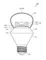
- FIG. 1 is a schematic diagram illustrating a configuration of a lighting device 10 described in Patent Document 1.
- the lighting device 10 includes a plurality of LEDs 12 arranged on a substrate, and a cylindrical case 14 made of a light transmissive material arranged around the LEDs 12.
- the upper surface of the case 14 is formed in an inverted truncated cone shape.
- An aluminum plate (light flux controlling member) 16 that reflects light is attached to the inclined surface of the truncated cone and functions as a reflecting surface.
- the plane of the truncated cone functions as a transmission window 18 that transmits light.
- a part of the light emitted from the LED 12 disposed in the center portion passes through the transmission window 18 and becomes outgoing light in the forward direction (upward direction).
- part of the light emitted from the LED 12 is reflected by the aluminum plate 16 and becomes emitted light in the lateral direction (horizontal direction) and the backward direction (downward direction).
- the light flux controlling member as in Patent Document 1, the light distribution characteristic of the lighting device (LED light bulb) can be brought close to the light distribution characteristic of the incandescent light bulb to some extent.
- the illumination device 10 described in Patent Document 1 is configured to control the light emitted from the LED 12 disposed in the central portion, the light emitted from the LED 12 disposed in a region other than the central portion is used. It cannot be controlled properly.
- the LED 12 having a large light emitting surface is used, the light emitted from the outer peripheral portion of the light emitting surface cannot be appropriately controlled.
- the lighting device 10 described in Patent Document 1 has a problem that the balance of the light distribution characteristics is poor in this case.
- an object of the present invention is a light flux controlling member used in a lighting device having a light emitting element, and is a forward direction even when a plurality of light emitting elements are arranged or a light emitting element having a large light emitting surface is used.
- An object of the present invention is to provide a light flux controlling member capable of distributing light in a balanced manner in all of the lateral direction and the backward direction.
- Another object of the present invention is to provide a light emitting device and an illumination device having the light flux controlling member.
- the light flux controlling member is a light flux controlling member for controlling the light distribution of the light emitted from the light emitting element, and is disposed apart from the central axis so as to surround the central axis of the light flux controlling member.
- a first incident surface and a second incident surface disposed so as to surround the first incident surface, and an incident surface for allowing the light emitted from the light emitting element to enter the light flux controlling member; It is arranged on the opposite side of the incident surface so that the distance from the central axis gradually increases toward the upper side along the central axis, and a part of the light incident on the incident surface is separated from the central axis.
- An upper total reflection surface that reflects toward the direction and the central axis and the first incident surface so as to surround the central axis, and a part of the light incident on the first incident surface is partially reflected on the upper total reflection surface.
- Lower total reflection surface that reflects toward the reflection surface
- An exit surface that is disposed outside the upper total reflection surface so as to surround the central axis, and mainly emits light reflected by the upper total reflection surface to the outside, and the incident surface and the upper total reflection
- the surface, the lower total reflection surface, and the emission surface are rotationally symmetric with the central axis as a rotation axis.
- the light-emitting device includes one or more light-emitting elements and a light flux control member according to the present invention, and the light flux control member has a central axis of the light flux control member of the 1 or 2
- the light emitting elements are arranged so as to coincide with the optical axis of the light emitting element, and the light emitting surface of the one or more light emitting elements at a position farthest from the central axis is arranged to face the second incident surface.
- the lighting device according to the present invention includes the light emitting device according to the present invention and a cover that allows the light emitted from the light emitting device to pass through while diffusing.
- the illuminating device having the light flux controlling member of the present invention exhibits a light distribution characteristic closer to that of an incandescent bulb than a conventional illuminating device.
- FIG. 1 is a schematic diagram showing the configuration of the illumination device described in Patent Document 1.
- FIG. 2 is a partial cross-sectional view of the lighting apparatus according to Embodiment 1.
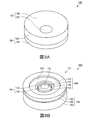
- 3A and 3B are perspective views of the light flux controlling member according to the first embodiment.
- 4A to 4C are diagrams showing the configuration of the light flux controlling member according to the first embodiment.
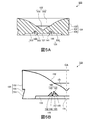
- 5A and 5B are cross-sectional views of the light flux controlling member according to the first embodiment.
- FIG. 6 is a diagram showing an optical path of light in the light flux controlling member according to the first embodiment.
- FIG. 7 is a graph illustrating light distribution characteristics of the light-emitting element, the light-emitting device, and the lighting device according to Embodiment 1.
- FIG. 1 is a schematic diagram showing the configuration of the illumination device described in Patent Document 1.
- FIG. 2 is a partial cross-sectional view of the lighting apparatus according to Embodiment 1.
- 3A and 3B are perspective views of the light flux controlling member according to the first embodiment
- FIG. 8A is a partial cross-sectional view of the lighting apparatus according to Embodiment 2
- FIG. 8B is a diagram showing the arrangement of light emitting elements in the lighting apparatus according to Embodiment 2.
- 9A to 9C are diagrams showing the configuration of the light flux controlling member according to the second embodiment.
- FIG. 10 is a cross-sectional view of the light flux controlling member according to the second embodiment.
- 11A and 11B are diagrams showing light paths of light in the light flux controlling member according to the second embodiment.
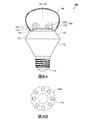
- FIG. 2 is a cross-sectional view showing a configuration of lighting apparatus 100 according to Embodiment 1 of the present invention.
- the lighting device 100 includes a light emitting device 130 including a light emitting element 110 and a light flux controlling member 120, a cover 160, and a housing 170.
- a light emitting device 130 including a light emitting element 110 and a light flux controlling member 120
- a cover 160 including a cover 160
- a housing 170 a housing 170.
- the light emitting element 110 is a light source of the lighting device 100 and is mounted on the housing 170.
- the light emitting element 110 is a light emitting diode (LED) such as a white light emitting diode.
- the number of the light emitting elements 110 may be singular or plural. Further, the size of the light emitting surface of the light emitting element 110 is not particularly limited. In the present embodiment, the number of the light emitting elements 110 is one, and the size of the light emitting elements 110 is larger than the third incident surface 131 and the first incident surface 132 of the light flux controlling member 120 described later.
- the light emitting surface (light emitting point) of the light emitting element 110 at the position farthest from the central axis CA is disposed so as to face a second incident surface 133 described later.
- the light emitting element 110 is arranged so that the optical axis OA thereof coincides with the central axis CA of the light flux controlling member 120.
- the “optical axis of the light emitting element” refers to the traveling direction of light at the center of the three-dimensional light flux from the light emitting element 110.
- the traveling direction of light at the center of a three-dimensional light beam from the plurality of light emitting elements 110 is referred to.
- the emission direction along the optical axis OA of the light emitting element 110 is defined as the front, and the opposite direction is defined as the rear.
- the light flux controlling member 120 controls the light distribution of the light emitted from the light emitting element 110.
- the light flux controlling member 120 is disposed in the housing 170 so that the central axis CA thereof coincides with the optical axis OA of the light emitting element 110. Since one of the features of the present invention is the shape of the light flux controlling member 120, details of the light flux controlling member 120 will be described later.
- the cover 160 has a hollow region including an opening.
- the light emitting device 130 is disposed in the hollow region of the cover 160.
- the cover 160 covers the light flux controlling member 120 and allows light emitted from the light flux controlling member 120 to pass through while diffusing.
- the cover 160 is light transmissive.
- the material of the cover 160 is light transmissive resin such as polymethyl methacrylate (PMMA), polycarbonate (PC), and epoxy resin (EP), or glass.
- the cover 160 also has light diffusibility.
- the means for imparting light diffusing power to the cover 160 is not particularly limited.
- a light diffusion process (for example, a roughening process) may be performed on the inner surface or the outer surface of the cover 160 made of a transparent material, or light diffusion including a scatterer such as a bead on the transparent material.
- the cover 160 may be manufactured by blending a material having a property.
- the cover 160 preferably has a rotationally symmetric shape with respect to the optical axis OA.
- the shape of the cover 160 may be, for example, a shape including only a rotationally symmetric shape, or may be a shape including a part of the rotationally symmetric shape.
- the shape of the cover 160 is preferably a shape that can further improve the balance of light distribution of light emitted from the light flux controlling member 120.
- the shape of the cover 160 is preferably a shape in which the diameter of the opening of the cover 160 is smaller than the maximum outer diameter of the cover 160 from the viewpoint of increasing the amount of light to the rear.
- the shape of the cover 160 is, for example, a spherical crown shape (a shape obtained by cutting a part of a spherical surface with a plane).
- the maximum outer diameter of the cover 160 is, for example, 60 mm, and the opening diameter of the cover 160 is, for example, 38 mm (see FIG. 2).
- the housing 170 supports the light emitting element 110, the light flux controlling member 120, and the cover 160 at the front end of the housing 170, respectively.
- the housing 170 is a rotationally symmetric body with the optical axis OA as the rotation axis.
- the housing 170 is disposed in front of the base 171 and the base 171, and the first tapered surface 172 whose distance from the central axis CA gradually increases toward the front, and as it goes forward from the front end edge of the first tapered surface 172.
- a second tapered surface 173 whose distance from the central axis CA gradually decreases, and an annular end surface 174 formed in an annular plane perpendicular to the central axis CA, which is formed on the inner side from the front end edge of the second tapered surface 173;
- a columnar protrusion 175 protruding forward from the inner peripheral edge of the annular end surface 174.
- a substrate (not shown) is attached to the circular front end surface of the protrusion 175, and the light emitting element 110 is mounted on the substrate.
- the distance from the annular end surface 174 to the front end surface of the protruding portion 175 (the protruding length of the protruding portion 175) is, for example, 3 mm.
- the opening of the cover 160 is in contact with the annular end surface 174.
- the outer diameter of the annular end surface 174 is substantially the same as the outer diameter of the opening of the cover 160.
- the annular end surface 174 is a pedestal with which the opening of the cover 160 abuts.
- the second tapered surface 173 is a tapered surface in which the distance from the central axis CA gradually increases from the periphery of the pedestal toward the rear.
- a power supply circuit (not shown) that electrically connects the base 171 and the light emitting element 110 is disposed in a portion surrounded by the first tapered surface 172 and the second tapered surface 173 of the housing 170.
- the housing 170 also serves as a heat sink for releasing heat from the light emitting element 110.
- casing 170 is comprised with metals with high heat conductivity, such as aluminum and copper.
- the light emitted from the light emitting element 110 is controlled by the light flux controlling member 120 so as to go in all directions.
- the light emitted from the light flux controlling member 120 passes through the cover 160 while diffusing.
- FIGS. 4A to 4C, and FIGS. 5A and 5B are diagrams showing the configuration of the light flux controlling member 120.
- FIG. 3A is a perspective view of the light flux controlling member 120 viewed from the front
- FIG. 3B is a perspective view of the light flux controlling member 120 viewed from the rear.
- 4A is a plan view of the light flux controlling member 120
- FIG. 4B is a bottom view
- FIG. 4C is a side view.
- 5A is a cross-sectional view taken along line AA shown in FIG. 4A
- FIG. 5B is a partially enlarged view of FIG. 5A. 3 to 5, the leg portion 125 is omitted.
- the light flux controlling member 120 includes an incident surface 121, an upper total reflection surface 122 including a first total reflection surface 151 and a second total reflection surface 152, and a lower total reflection surface 123. , And an emission surface 124.
- the light flux controlling member 120 is rotationally symmetric with the central axis CA as the rotation axis. Further, in the present embodiment, light flux controlling member 120 forms a gap for releasing heat generated from light emitting element 110 to the outside, and has leg portion 125 for fixing to housing 170 ( (See FIG. 2).
- the incident surface 121 allows the light emitted from the light emitting element 110 to enter the light flux controlling member 120.
- the incident surface 121 includes a third incident surface 131, a first incident surface 132, and a second incident surface 133.
- the incident surface 121 is at least a part of the inner surface of the recess formed on the back side of the light flux controlling member 120.
- the third incident surface 131 is disposed to face the light emitting element 110 so as to intersect the central axis CA (the optical axis OA of the light emitting element 110).
- the shape of the third entrance surface 131 is not particularly limited.
- the shape of the third entrance surface 131 may be a flat surface or a curved surface.
- the third incident surface 131 is planar.
- the planar view shape of the 3rd entrance plane 131 is circular. That is, the third incident surface 131 is rotationally symmetric with the central axis CA as the rotation axis.
- the third incident surface 131 allows a large amount of light to enter the light emitted from the central portion of the light emitting element 110.
- the first incident surface 132 is disposed so as to surround the third incident surface 131. In other words, the first incident surface 132 is disposed away from the central axis CA so as to surround the central axis CA.
- the first incident surface 132 is rotationally symmetric with the central axis CA as the rotation axis.
- the first incident surface 132 is a first outer inclined surface in the annular convex portion 144 including the first inner inclined surface 145 and the first outer inclined surface, which is disposed in the annular concave portion 141 surrounding the central axis CA.
- the annular recess 141 is disposed so as to surround the third incident surface 131.
- the annular recess 141 has an annular second inner inclined surface 142 disposed on the central axis CA side (inner side) and an annular second outer inclined surface 143 disposed on the outer edge side (outer side). .
- the depth of the annular concave portion 141 is the same as the height of the annular convex portion 144.
- the depth of the annular recess 141 is preferably such a depth that the light incident on the third incident surface 131 and totally reflected on the upper total reflection surface 122 does not reach directly. If the light incident on the third incident surface 131 and totally reflected on the upper total reflection surface 122 reaches the second inner inclined surface 142 directly, the light distribution may not be appropriately controlled.
- the second inner inclined surface 142 is rotationally symmetric with the central axis CA as the rotation axis.
- the second inner inclined surface 142 is formed so as to be away from the reference plane that is orthogonal to the central axis CA and passes through the intersection of the third incident surface 131 and the central axis CA as the distance from the central axis CA increases.
- the generatrix from the central axis CA to the outer edge of the second inner inclined surface 142 may be a straight line or a curved line. In the present embodiment, the generatrix from the central axis CA to the outer edge of the second inner inclined surface 142 is a straight line.
- the inclination angle of the second inner inclined surface 142 with respect to the central axis CA is not particularly limited, but is preferably set in consideration of light incident on the third incident surface 131. That is, the inclination angle of the second inner inclined surface 142 with respect to the central axis CA is preferably an angle at which the light emitted from the light emitting element 110 and incident on the third incident surface 131 does not reach directly. If the light incident from the third incident surface 131 reaches the second inner inclined surface 142 directly, the light distribution may not be appropriately controlled.
- the second outer inclined surface 143 is rotationally symmetric with the central axis CA as the rotation axis.
- the second outer inclined surface 143 is formed so as to approach the reference plane as the distance from the central axis CA increases.
- the generatrix from the center side of the second outer inclined surface 143 to the outer edge may be a straight line or a curved line.
- the bus line from the central axis CA to the outer edge portion of the second outer inclined surface 143 is a straight line.
- the inclination angle of the second outer inclined surface 143 with respect to the central axis CA is not particularly limited and is appropriately set.
- the outer edge of the second outer inclined surface 143 is separated from the central axis CA from the boundary between the first total reflection surface 151 and the second total reflection surface 152 in a direction orthogonal to the optical axis OA of the cross section including the optical axis OA. It is arranged at the position.
- the annular convex portion 144 is disposed inside the annular concave portion 141.
- the annular convex portion 144 has an annular first inner inclined surface 145 disposed on the central axis CA side (inner side) and an annular first outer inclined surface disposed on the outer edge side (outer side).
- the 1st connection surface 147 may be arrange
- the first inner inclined surface 145 is rotationally symmetric with the central axis CA as the rotation axis.
- the first inner inclined surface 145 is connected to the outer edge portion of the second inner inclined surface 142.
- the first inner inclined surface 145 is formed so as to approach the reference plane as the distance from the central axis CA increases. It is preferable that the bus line from the central axis CA to the outer edge portion of the first inner inclined surface 145 is a straight line.
- the first inner inclined surface 145 functions as a part of the lower total reflection surface 123 that reflects the light incident on the first outer inclined surface.
- the first outer inclined surface (first incident surface 132) is rotationally symmetric with the central axis CA as a rotation axis.
- the first outer inclined surface is connected to the inner edge of the second outer inclined surface 143.
- the first outer inclined surface is formed so as to be away from the reference plane as it is away from the central axis CA.
- the generatrix line from the central axis CA to the outer edge of the first outer inclined surface may be a straight line or a curved line.
- the bus line from the central axis CA to the outer edge portion of the first outer inclined surface (first incident surface 132) is a straight line.
- the inner edge of the first outer inclined surface is preferably disposed on the same plane as the third incident surface 131.
- the first outer inclined surface (first incident surface 132) is a portion of the light emitted from the light emitting elements 110 disposed on the outer peripheral portion of the protrusion 175.
- the light traveling toward the optical axis OA is incident and the light emitting element 110 includes the light emitting element 110 including a large light emitting surface, the light traveling toward the optical axis OA side out of the light emitted from the outer peripheral portion of the light emitting surface. Make it incident.
- the first connection surface 147 connects the first inner inclined surface 145 and the first outer inclined surface (first incident surface 132).
- a ridge line 148 is formed at the boundary between the first connection surface 147 and the first outer inclined surface.
- the ridge line 148 is preferably arranged on the same plane as the third incident surface 131.
- the boundary between the first inner inclined surface 145 and the first outer inclined surface (first incident surface 132) is a ridge line 148.
- the first inner inclined surface 145 and the first connection surface 147 constitute a lower total reflection surface 123.
- the second incident surface 133 is disposed so as to surround the first incident surface 132.
- the shape of the second incident surface 133 is not particularly limited.
- the shape of the second incident surface 133 may be a flat surface or a curved surface.
- the second incident surface 133 is planar.
- the planar view shape of the second incident surface 133 is an annular shape.
- the second incident surface 133 is a part of other light (e.g., light emitted from the light emitting elements 110 disposed on the outer peripheral portion of the protrusion 175).
- the other part of the light emitted from the outer peripheral portion of the light emitting surface. (Not toward the first incident surface 132) is incident. That is, the second incident surface 133 is disposed to face the light emitting point of the light emitting element 110 at the position farthest from the central axis CA.
- the second incident surface 133 may be disposed at the same position (height) as the third incident surface 131 in the direction of the central axis CA, or may be disposed at a different position (height). In the present embodiment, the positions (heights) of the second incident surface 133 and the third incident surface 131 are the same in the direction of the central axis CA.
- the upper total reflection surface 122 is disposed on the opposite side of the incident surface 121 so as to move away from the reference plane from the central axis CA toward the outer edge. In other words, the upper total reflection surface 122 is arranged so that the distance from the central axis CA gradually increases along the central axis CA and toward the upper side.
- the upper total reflection surface 122 is rotationally symmetric with the central axis CA as a rotation axis.
- the upper total reflection surface 122 reflects a part of the light incident on the incident surface 121 in a direction away from the central axis CA.
- upper total reflection surface 122 includes first total reflection surface 151 disposed on the central axis CA side, and second total reflection surface 152 disposed on the outer edge.
- the first total reflection surface 151 is disposed on the central axis CA side.
- the first total reflection surface 151 is rotationally symmetric with the central axis CA as a rotation axis.
- the first total reflection surface 151 has a rotationally symmetric aspherical shape.
- the generatrix line from the central axis CA to the outer edge portion of the first total reflection surface 151 is a curve that moves away from the reference plane as it goes from the central axis CA to the outer edge portion. More specifically, in the cross section including the central axis CA, the first total reflection surface 151 is a curve in which the tangential gradient gradually decreases from the central axis CA toward the outer edge.
- the curve may not be an arc as in the present embodiment, but may be an arc.
- one curve having the central axis CA as a boundary may be formed with a predetermined first curvature.
- the first total reflection surface 151 reflects a large amount of light (light having a small angle with respect to the central axis CA) out of the light incident on the third incident surface 131 toward the emission surface 124.
- the second total reflection surface 152 is disposed so as to surround the first total reflection surface 151.
- the second total reflection surface 152 is rotationally symmetric with the central axis CA as the rotation axis.
- second total reflection surface 152 has a rotationally symmetric aspheric shape.
- the generatrix from the center of the second total reflection surface 152 to the outer edge is a curve that moves away from the reference plane from the central axis CA toward the outer edge. More specifically, in the cross section including the central axis CA, the second total reflection surface 152 is a curve in which the tangential gradient gradually decreases from the central axis CA toward the outer edge.
- the curve may not be an arc as in the present embodiment, but may be an arc.
- one curve having the central axis CA as a boundary may be formed with a second curvature different from the first curvature.
- the first total reflection surface 151 and the second total reflection surface 152 are each formed with an arc having a predetermined curvature, the first total reflection surface 151 may be formed with a curvature larger than the second curvature.
- the total reflection surface 151 and the second total reflection surface 152 may be formed with the same curvature by shifting the position of the center of curvature.
- the inclination of the tangential line on the most central axis CA side of the second total reflection surface 152 is far from the most central axis CA of the first total reflection surface 151. Greater than the slope of the tangent at that position.
- the second total reflection surface 152 is incident on the first incident surface 132 and is reflected by the lower total reflection surface 123 described later, and the light incident on the third incident surface 131 is the first total reflection surface 151.
- the light that has not reached (the light having a large angle with respect to the central axis CA) is reflected toward the emission surface 124.
- the boundary between the first total reflection surface 151 and the second total reflection surface 152 is set as appropriate. As described above, light that is incident mainly on the first incident surface 132 and reflected by the lower total reflection surface 123 is reflected by the second total reflection surface 152. Therefore, the boundary between the first total reflection surface 151 and the second total reflection surface 152 in the direction orthogonal to the central axis CA is disposed so as to be located on the outer peripheral portion from the lower total reflection surface 123 described later.
- the lower total reflection surface 123 has the first inner inclined surface 145 as described above.
- lower total reflection surface 123 includes first inner inclined surface 145 and first connection surface 147.
- the lower total reflection surface 123 is disposed between the third incident surface 131 and the first incident surface 132 so as to surround the central axis CA.
- the lower total reflection surface 123 reflects the light incident on the first incident surface 132 toward the second total reflection surface 152.
- the annular convex portion 144 does not have the first connection surface 147
- the first inner inclined surface 145 functions as the lower total reflection surface 123.
- the lower total reflection surface 123 may be formed as a curved surface having a curvature changed in a direction along the central axis CA.
- the emission surface 124 is disposed outside the upper total reflection surface 122 so as to surround the central axis CA.
- the emission surface 124 is rotationally symmetric with the central axis CA as the rotation axis.
- the emission surface 124 emits the light reflected by the upper total reflection surface 122 to the outside.
- the exit surface 124 has a first exit surface 153 and a second exit surface 154.
- the first emission surface 153 is disposed forward in the direction along the central axis CA.
- the first emission surface 153 is cylindrical.
- the second emission surface 154 is disposed rearward in the direction along the central axis CA.
- the second emission surface 154 is formed so as to approach the reference plane as the distance from the central axis CA increases.
- a bus line from the central axis CA side of the second emission surface 154 toward the outer edge portion is a straight line.
- a step surface 155 is formed between the first emission surface 153 and the second emission surface 154.
- the step surface 155 is disposed in parallel with the third incident surface 131 (second incident surface 133).
- the position of the step surface 155 on the exit surface 124 is not particularly limited.
- step surface 155 is formed at the same height as first total reflection surface 151 in the direction along central axis CA.
- exit surface 124 may not have the step surface 155. In this case, the first emission surface 153 and the second emission surface 154 are connected.
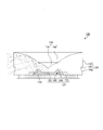
- FIG. 6 is an optical path diagram of the light flux controlling member 120 that does not have the leg portion 125 of the light emitted from the light emitting element 110.
- a broken line in FIG. 6 indicates an optical path of light emitted from the center of the light emitting element 110, and a dotted line indicates an optical path of light emitted from the end of the light emitting element 110. Since light flux controlling member 120 according to the present embodiment is rotationally symmetric with respect to central axis CA as a rotational axis, only the optical path in the left half of light flux controlling member 120 is shown in the cross section including central axis CA in FIG. Yes.
- most of the light emitted from the end portion of the light emitting surface of the light emitting element 110 is a light flux controlling member on the first incident surface 132 and the second incident surface 133.
- Incident 120 The light incident on the first incident surface 132 (first outer inclined surface) is totally reflected by the lower total reflection surface 123 and travels toward the second total reflection surface 152 (upper total reflection surface 122).
- the light that has reached the second total reflection surface 152 is totally reflected toward the emission surface 124 (second emission surface 154).
- the light emitted from the end portion of the light emitting element 110 and incident on the second incident surface 133 travels toward the second total reflection surface 152 (upper total reflection surface 122).
- the light that reaches the second total reflection surface 152 is totally reflected toward the emission surface 124 (first emission surface 153). Of the light that has reached the exit surface 124 (the first exit surface 153 and the second exit surface 154), a lot of light is emitted toward the rear of the light flux controlling member 120. Note that the light emitted from the light emitting element 110 is similarly controlled even when the light emitting element 110 is provided. In this case, the light emitted from the light emitting element 110 disposed on the outer peripheral portion of the front end face of the protrusion 175 corresponds to the light emitted from the end of the light emitting element 110 in the present embodiment.
- the light distribution characteristics of the light emitting device 130 having one light emitting element 110 and one light flux controlling member 120, and the light emitting device 130 The light distribution characteristics of the lighting device 100 to which the cover 160 was attached were simulated. Specifically, relative illuminance in all directions on a plane including the optical axis OA was obtained using the light emission center of the light emitting element 110 as a reference point. In this simulation, the illuminance on a virtual surface at a distance of 1000 mm from the light emission center of the light emitting element 110 was calculated. For comparison, the light distribution characteristic of only the light emitting element 110 was also simulated.
- FIG. 7 is a graph showing the light distribution characteristics of the light emitting element 110, the light emitting device 130, and the lighting device 100.
- a numerical value described outside the graph indicates an angle (°) with respect to the light emission center of the light emitting element 110. 0 ° indicates the optical axis direction (front direction), 90 ° indicates the horizontal direction (side direction), and 180 ° indicates the rear direction.
- the numerical value described inside the graph has shown the relative illumination intensity (maximum value 1) of each direction.
- the dotted line in the graph indicates the result when only the light emitting element 110 is used, the solid line indicates the result when the light emitting element 110 and the light flux controlling member 120 are combined (the light emitting device 130), and the broken line indicates The result when the light emitting element 110, the light flux controlling member 120, and the cover 160 are combined (the illumination device 100) is shown.
- the light emitting device 130 appropriately generates light traveling in the direction of ⁇ 120 to 150 ° in addition to light traveling forward. This is considered to be because the light emitted from the end portion of the light emitting element 110 can be appropriately controlled in the backward direction by the lower total reflection surface 123.
- the unevenness of light can be reduced by equalizing the amount of light emitted toward the front direction, the side direction, and the rear direction.
- the illumination device 100 having the light flux controlling member 120 according to Embodiment 1 of the present invention has the lower total reflection surface 123 for controlling the light emitted from the outer peripheral portion of the light emitting element 110. Therefore, not only the light emitted from the center of the light emitting element 110 but also the light emitted from the outer peripheral portion of the light emitting element 110 can be appropriately controlled. Therefore, the illuminating device 100 which concerns on this invention can show the light distribution characteristic close
- the lighting device 200 according to the second embodiment is different from the lighting device 100 according to the first embodiment in the configuration of the light emitting device 230. Therefore, the same components as those in the first embodiment are denoted by the same reference numerals and description thereof is omitted.
- FIG. 8A is a cross-sectional view illustrating a configuration of lighting apparatus 200 according to Embodiment 2 of the present invention
- FIG. 8B is a plan view illustrating an arrangement of light emitting elements 110 in lighting apparatus 200 according to Embodiment 2.
- the lighting device 200 includes a light emitting device 230 including the light emitting element 110 and the light flux controlling member 220, a cover 160, and a housing 170.
- the light emitting element 110 is mounted on a substrate (not shown) attached to the housing 170.
- the number of the light emitting elements 110 is not particularly limited as long as it is plural. In the present embodiment, the number of light emitting elements 110 is eight, and they are arranged at equal intervals in the circumferential direction.
- the optical axis OA of each light emitting element 110 is disposed so as to intersect the light flux controlling member 220. Further, the light emitting surface of the light emitting element 110 is disposed so as to face the second incident surface 133.
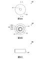
- FIG. 9A to 9C and FIG. 10 are diagrams showing the configuration of the light flux controlling member 220.
- FIG. 9A is a plan view of the light flux controlling member 220
- FIG. 9B is a bottom view
- FIG. 9C is a side view.
- FIG. 10 is a cross-sectional view taken along line AA shown in FIG. 9A. 9A to 9C and FIG. 10, the leg portion 125 is omitted.
- the light flux controlling member 220 includes an incident surface 221, an upper total reflection surface 222 including a second total reflection surface 152, a lower total reflection surface 123, and an output surface 224. And having.
- light flux controlling member 220 has leg portion 125.
- the incident surface 221 has a first incident surface 132 and a second incident surface 133.
- the first incident surface 132 is a first outer inclined surface in the annular convex portion 144 including the first inner inclined surface 145, the first connection surface 147, the ridge line 148, and the first outer inclined surface.
- An annular second outer inclined surface 143 is disposed outside the first incident surface 132.
- the second total reflection surface 152 (upper total reflection surface 222) is such that the distance from the central axis CA gradually increases toward the upper side (the emission direction of the light emitted from the light emitting element 110) along the central axis CA. Is formed.
- the emission surface 224 is rotationally symmetric with the central axis CA as a rotation axis, and is formed in a cylindrical shape. Note that the emission surface 224 may be composed of a plurality of surfaces.
- light flux controlling member 220 has a through hole at the center and does not have third incident surface 131 and first total reflection surface 151.
- the end of the upper total reflection surface 222 (second total reflection surface 152) on the central axis CA side and the end of the incident surface 221 (first inner inclined surface 145) on the central axis CA side are second connected. Connected by a surface 247.
- FIGS. 11A and 11B are optical path diagrams of the light flux controlling member 220 for the light emitted from the light emitting element 110.
- FIG. FIG. 11A shows an optical path of light emitted from the light emitting element 110 and emitted from the optical axis OA of the light emitting element 110 toward the central axis CA.
- FIG. 11B shows the light path emitted from the light emitting element 110.
- An optical path of light emitted from the optical axis OA 110 toward the outer edge side is shown. Since light flux controlling member 220 according to the present embodiment is rotationally symmetric with respect to central axis CA as the rotational axis, only the optical path in the left half of light flux controlling member 220 in the cross section including central axis CA in FIGS. 11A and 11B. Show. Further, in FIGS. 11A and 11B, the leg portion 125 is omitted.
- the first incident surface 132 As shown in FIG. 11A, among the light emitted from the light emitting element 110 and emitted from the optical axis OA of the light emitting element 110 toward the central axis CA, light having a small emission angle is emitted from the first incident surface 132.
- the light enters the light flux controlling member 220.
- the light incident on the first incident surface 132 (first outer inclined surface) is totally reflected by the lower total reflection surface 123 and travels toward the second total reflection surface 152 (upper total reflection surface 122).
- the light that reaches the second total reflection surface 152 is totally reflected toward the emission surface 224.
- the light totally reflected by the second total reflection surface 152 is emitted toward the side or rear of the light flux controlling member 220.
- the light having a large emission angle is located on the opposite side across the central axis CA. Is emitted toward the side or rear of the light flux controlling member 220.
- a part of the light is incident on the second outer inclined surface 143 and is second. The light is emitted from the total reflection surface 152 to the outside.
- most of the light emitted from the light emitting element 110 and emitted toward the outer edge side from the optical axis OA of the light emitting element 110 is the second incident surface 133 or the second light.
- the light enters the light flux controlling member 220 at the outer inclined surface 143.
- Most of the light incident on the second incident surface 133 or the second outer inclined surface 143 is totally reflected by the second total reflection surface 152 toward the emission surface 124 (second emission surface 154).
- the light totally reflected by the second total reflection surface 152 is emitted toward the side or rear of the light flux controlling member 220.
- the illumination device 200 having the light flux controlling member 220 according to Embodiment 2 of the present invention has the lower total reflection surface 123, and thus the light emitting element 110 is arranged in the circumferential direction. Even so, the light emitted from the light emitting element 110 can be appropriately controlled. Therefore, the illuminating device 200 according to the present invention can exhibit a light distribution characteristic closer to that of an incandescent lamp as compared with a conventional illuminating device.
- the lighting device of the present invention can be used in place of an incandescent bulb, it can be widely applied to various lighting devices such as chandeliers and indirect lighting devices.
Abstract
本発明の光束制御部材(120)は、その中心軸を取り囲むように、中心軸から離間して配置された第1入射面(132)および第1入射面を取り囲んで配置された第2入射面(133)を含む入射面(121)と、中心軸に沿って上側に向かうにつれて、中心軸からの距離が漸増するように入射面の反対側に配置され、入射面で入射した光を、中心軸から離れる方向に反射させる上側全反射面(122)と、中心軸を取り囲んで中心軸および第1入射面の間に配置され、第1入射面で入射した光の一部を上側全反射面に反射させる下側全反射面(123)と、中心軸を取り囲んで上側全反射面より外側に配置され、上側全反射面で反射した光を外部に出射させる出射面(124)とを有する。
Description
本発明は、発光素子から出射された光の配光を制御する光束制御部材、当該光束制御部材を有する発光装置および照明装置に関する。
近年、省エネルギーや環境保全の観点から、発光ダイオード(以下「LED」ともいう)を光源とする照明装置(例えば、LED電球)が、白熱電球に代わるものとして使用されている。しかしながら、従来のLEDを光源とする照明装置は、前方方向のみに光を出射し、白熱電球のように幅広い方向に光を出射することができない。このため、従来の照明装置は、白熱電球のように天井や壁面からの反射光を利用して室内を広範囲に照らすことができない。
従来のLEDを光源とする照明装置の配光特性を白熱電球の配光特性に近づけるため、LEDからの出射光の配光を光束制御部材で制御することが提案されている(例えば、特許文献1参照)。図1は、特許文献1に記載の照明装置10の構成を示す模式図である。図1に示されるように、照明装置10は、基板上に配置された複数のLED12と、LED12の周囲に配置された光透過性材料からなる円筒形のケース14とを有する。ケース14の上面は、逆円錐台形状に形成されている。円錐台の斜面は、光を反射させるアルミ板(光束制御部材)16が貼り付けられており、反射面として機能する。一方、円錐台の平面は、光を透過させる透過窓18として機能する。図1において矢印で示されるように、中心部に配置されたLED12から出射された光の一部は、透過窓18を通過して前方方向(上方向)への出射光となる。また、LED12から出射された光の一部は、アルミ板16で反射して側方方向(水平方向)および後方方向(下方向)への出射光となる。
このように光束制御部材を用いて中心部に配置されたLEDからの出射光の進行方向を制御することにより、前方方向だけでなく、側方方向および後方方向への出射光を得ることができる。したがって、特許文献1に記載の光束制御部材(アルミ板)を使用することで、照明装置(LED電球)の配光特性を白熱電球の配光特性にある程度近づけることができる。
しかしながら、特許文献1に記載の照明装置10では、中心部に配置されたLED12から出射された光を制御するように構成されているため、中心部以外に配置されたLED12から出射された光を適切に制御できない。また、発光面の大きいLED12を用いた場合にも同様に、発光面の外周部から出射された光を適切に制御できない。結果として、特許文献1に記載の照明装置10では、この場合に配光特性のバランスが悪いという問題がある。
そこで、本発明の目的は、発光素子を有する照明装置に用いられる光束制御部材であって、複数の発光素子を配置した場合、または発光面の大きい発光素子を用いた場合であっても前方方向、側方方向および後方方向のすべてにバランスよく配光することができる光束制御部材を提供することである。また、本発明の別の目的は、この光束制御部材を有する発光装置および照明装置を提供することである。
本発明に係る光束制御部材は、発光素子から出射された光の配光を制御する光束制御部材であって、前記光束制御部材の中心軸を取り囲むように、前記中心軸から離間して配置された第1入射面と、前記第1入射面を取り囲むように配置された第2入射面とを含み、前記発光素子から出射された光を、前記光束制御部材の内部に入射させる入射面と、前記中心軸に沿って上側に向かうにつれて、前記中心軸からの距離が漸増するように、前記入射面の反対側に配置され、前記入射面で入射した光の一部を、前記中心軸から離れる方向に向けて反射させる上側全反射面と、前記中心軸を取り囲むように前記中心軸および前記第1入射面の間に配置され、前記第1入射面で入射した光の一部を前記上側全反射面に向けて反射させる下側全反射面と、前記中心軸を取り囲むように前記上側全反射面より外側に配置され、主として前記上側全反射面で反射した光を外部に出射させる出射面と、を有し、前記入射面、前記上側全反射面、前記下側全反射面および前記出射面は、前記中心軸を回転軸とする回転対称である。
また、本発明に係る発光装置は、1または2以上の発光素子と、本発明に係る光束制御部材と、を有し、前記光束制御部材は、前記光束制御部材の中心軸が前記1または2以上の発光素子の光軸と合致するように配置されており、前記中心軸から最も離れた位置における前記1または2以上の発光素子の発光面は、前記第2入射面と向かい合って配置されている。
また、本発明に係る照明装置は、本発明に係る発光装置と、前記発光装置からの出射光を拡散させつつ透過させるカバーと、を有する。
本発明の光束制御部材を有する照明装置は、従来の照明装置に比べて、より白熱電球に近い配光特性を示す。
以下、本発明の実施の形態について、図面を参照して詳細に説明する。以下の説明では、本発明の照明装置の代表例として、白熱電球に代えて使用されうる照明装置について説明する。
[実施の形態1]
(照明装置の構成)
図2は、本発明の実施の形態1に係る照明装置100の構成を示す断面図である。なお、図2では、発光装置130およびカバー160のみを断面で示している。図2に示されるように、照明装置100は、発光素子110および光束制御部材120を含む発光装置130と、カバー160および筐体170を有する。以下、各構成要素について説明する。
(照明装置の構成)
図2は、本発明の実施の形態1に係る照明装置100の構成を示す断面図である。なお、図2では、発光装置130およびカバー160のみを断面で示している。図2に示されるように、照明装置100は、発光素子110および光束制御部材120を含む発光装置130と、カバー160および筐体170を有する。以下、各構成要素について説明する。
発光素子110は、照明装置100の光源であり、筐体170に実装されている。たとえば、発光素子110は、白色発光ダイオードなどの発光ダイオード(LED)である。発光素子110の数は、単数でも複数でもよい。また、発光素子110の発光面の大きさも特に限定されない。本実施の形態では、発光素子110の数は1つであり、発光素子110の大きさは、後述の光束制御部材120の第3入射面131および第1入射面132より大きい。また、中心軸CAから最も離れた位置における発光素子110の発光面(発光点)は、後述の第2入射面133と向かい合って配置されている。発光素子110は、その光軸OAが光束制御部材120の中心軸CAと一致するように配置される。ここで、「発光素子の光軸」とは、発光素子110からの立体的な光束の中心における光の進行方向を言う。発光素子110が複数ある場合は、複数の発光素子110からの立体的な光束の中心における光の進行方向を言う。以下、発光素子110の光軸OAに沿う出射方向を前方とし、その反対の方向を後方とする。
光束制御部材120は、発光素子110から出射された光の配光を制御する。光束制御部材120は、その中心軸CAが発光素子110の光軸OAと一致するように筐体170に配置される。本発明の特徴の一つは、光束制御部材120の形状であるため、光束制御部材120の詳細は、後述する。
カバー160は、開口部を含む中空領域を有する。発光装置130は、カバー160の中空領域内に配置される。
カバー160は、光束制御部材120を覆い、光束制御部材120から出射した光を拡散させつつ透過させる。カバー160は、光透過性を有する。たとえば、カバー160の材料は、ポリメタクリル酸メチル(PMMA)やポリカーボネート(PC)、エポキシ樹脂(EP)などの光透過性樹脂、またはガラスである。カバー160は、光拡散性も有する。カバー160に光拡散能を付与する手段は、特に限定されない。たとえば、透明な材料で作製されたカバー160の内面または外面に光拡散処理(例えば、粗面化処理)を行ってもよいし、上記の透明な材料に、ビーズなどの散乱子を含む光拡散性の材料を配合してカバー160を作製してもよい。
カバー160は、光軸OAに対して回転対称な形状を有することが好ましい。カバー160の形状は、例えば、回転対称な形状のみからなる形状であってもよいし、回転対称な形状の一部分を含む形状であってもよい。カバー160の形状は、光束制御部材120からの出射光の配光のバランスをさらに改善することができる形状であることが好ましい。たとえば、カバー160の形状は、後方への光の光量をより多くする観点から、カバー160の最大外径に比べてカバー160の開口部の径が小さい形状であることが好ましい。カバー160の形状は、例えば球冠形状(球面の一部を平面で切り取った形状)である。カバー160の最大外径は、例えば60mmであり、カバー160の開口径は、例えば38mmである(図2参照)。
筐体170は、発光素子110、光束制御部材120およびカバー160を、筐体170の前方端部でそれぞれ支持する。筐体170は、光軸OAを回転軸とする回転対称体である。筐体170は、口金171と、口金171の前方に配置され、前方に向かうにつれて中心軸CAからの距離が漸増する第1テーパー面172と、第1テーパー面172の前端縁から前方に向かうにつれて中心軸CAからの距離が漸減する第2テーパー面173と、第2テーパー面173の前端縁から内側に形成される、中心軸CAに垂直な円環状の平面で構成される環状端面174と、環状端面174の内周縁から前方に突出する円柱状の突出部175と、を有している。
突出部175の円形の前端面には基板(図示せず)が取り付けられ、その基板には発光素子110が実装されている。環状端面174から突出部175の前端面までの距離(突出部175の突出長さ)は、例えば3mmである。環状端面174には、カバー160の開口部が当接している。環状端面174の外径は、カバー160の開口部の外径とほぼ同じである。環状端面174は、カバー160の開口部が当接する台座となっている。第2テーパー面173は、上記台座の周縁から後方に向かうにつれて中心軸CAからの距離が漸増するテーパー面となっている。
筐体170の第1テーパー面172および第2テーパー面173で囲まれる部分の内部には、口金171と発光素子110とを電気的に接続する不図示の電源回路が配設されている。また、筐体170は、発光素子110からの熱を放出するためのヒートシンクを兼ねている。このため、筐体170は、アルミニウムや銅などの熱伝導性の高い金属によって構成されていることが好ましい。
発光素子110から出射された光は、光束制御部材120によって全方向に向かうように制御される。光束制御部材120から出射された光は、カバー160を拡散しつつ透過する。
(光束制御部材の構成)
ここで、光束制御部材120について詳細に説明する。図3A、B、図4A~Cおよび図5A、Bは、光束制御部材120の構成を示す図である。図3Aは、光束制御部材120を前方から見た斜視図であり、図3Bは、後方から見た斜視図である。図4Aは、光束制御部材120の平面図であり、図4Bは、底面図であり、図4Cは、側面図である。図5Aは、図4Aに示されるA-A線の断面図であり、図5Bは、図5Aの部分拡大図である。なお、図3~図5では、脚部125を省略している。
ここで、光束制御部材120について詳細に説明する。図3A、B、図4A~Cおよび図5A、Bは、光束制御部材120の構成を示す図である。図3Aは、光束制御部材120を前方から見た斜視図であり、図3Bは、後方から見た斜視図である。図4Aは、光束制御部材120の平面図であり、図4Bは、底面図であり、図4Cは、側面図である。図5Aは、図4Aに示されるA-A線の断面図であり、図5Bは、図5Aの部分拡大図である。なお、図3~図5では、脚部125を省略している。
図3A、Bに示されるように、光束制御部材120は、入射面121と、第1全反射面151および第2全反射面152を含む上側全反射面122と、下側全反射面123と、出射面124と、を有する。光束制御部材120は、中心軸CAを回転軸とした回転対称である。また、本実施の形態では、光束制御部材120は、発光素子110から発せられる熱を外部に逃がすための間隙を形成するとともに、筐体170に固定するための脚部125を有している(図2参照)。
入射面121は、発光素子110から出射された光を光束制御部材120の内部に入射させる。入射面121は、第3入射面131と、第1入射面132と、第2入射面133と、を有する。本実施の形態では、入射面121は、光束制御部材120の裏側に形成された凹部の内面の少なくとも一部である。
第3入射面131は、中心軸CA(発光素子110の光軸OA)と交わるように発光素子110と対向して配置される。第3入射面131の形状は特に限定されない。第3入射面131の形状は、平面状であってもよいし、曲面状であってもよい。本実施の形態では、第3入射面131は、平面状である。また、第3入射面131の平面視形状は、円形である。すなわち、第3入射面131は、中心軸CAを回転軸とする回転対称である。第3入射面131は、発光素子110の中央部分から出射された光のうち、多くの光を入射させる。
第1入射面132は、第3入射面131を取り囲むように配置される。言い換えると、第1入射面132は、中心軸CAを取り囲むように、中心軸CAから離間して配置されている。第1入射面132は、中心軸CAを回転軸とした回転対称である。第1入射面132は、中心軸CAを取り囲む環状凹部141内に配置された、第1内側傾斜面145および第1外側傾斜面を含む環状凸部144における第1外側傾斜面である。
環状凹部141は、第3入射面131を取り囲むように配置される。環状凹部141は、中心軸CA側(内側)に配置された円環状の第2内側傾斜面142と、外縁部側(外側)に配置された円環状の第2外側傾斜面143と、を有する。環状凹部141の深さは、環状凸部144の高さと同じである。環状凹部141の深さは、第3入射面131で入射して、上側全反射面122で全反射した光が直接到達しない程度の深さであることが好ましい。第3入射面131で入射して、上側全反射面122で全反射した光が第2内側傾斜面142に直接到達すると、配光を適切に制御できないおそれがある。
第2内側傾斜面142は、中心軸CAを回転軸とする回転対称である。第2内側傾斜面142は、中心軸CAから離れるにつれて、中心軸CAに直交し、かつ第3入射面131と中心軸CAとの交点を通る基準平面から離れるように形成されている。第2内側傾斜面142の中心軸CAから外縁部にかけての母線は、直線であってもよいし曲線であってもよい。本実施の形態では、第2内側傾斜面142の中心軸CAから外縁部にかけての母線は、直線である。中心軸CAに対する第2内側傾斜面142の傾斜角度は、特に限定されないが、第3入射面131で入射する光を考慮して設定されることが好ましい。すなわち、中心軸CAに対する第2内側傾斜面142の傾斜角度は、発光素子110から出射され、第3入射面131で入射した光が直接到達しない角度であることが好ましい。第3入射面131から入射した光が第2内側傾斜面142に直接到達すると、配光を適切に制御することができないおそれがある。
第2外側傾斜面143は、中心軸CAを回転軸とする回転対称である。第2外側傾斜面143は、中心軸CAから離れるにつれて、基準平面に近づくように形成されている。第2外側傾斜面143の中心側から外縁部にかけての母線は、直線であってもよいし曲線であってもよい。本実施の形態では、第2外側傾斜面143の中心軸CAから外縁部にかけての母線は、直線である。中心軸CAに対する第2外側傾斜面143の傾斜角度は、特に限定されず適宜設定される。また、第2外側傾斜面143の外縁は、光軸OAを含む断面の光軸OAに直交する方向において、第1全反射面151および第2全反射面152の境界より前記中心軸CAから離れた位置に配置されている。
前述の通り、環状凸部144は、環状凹部141の内部に配置されている。環状凸部144は、中心軸CA側(内側)に配置された円環状の第1内側傾斜面145と、外縁部側(外側)に配置された円環状の第1外側傾斜面と、を有する。なお、第1内側傾斜面145および第1外側傾斜面の間には、第1接続面147が配置されていてもよい。
第1内側傾斜面145は、中心軸CAを回転軸とする回転対称である。第1内側傾斜面145は、第2内側傾斜面142の外縁部に接続されている。第1内側傾斜面145は、中心軸CAから離れるにつれて、基準平面に近づくように形成されている。第1内側傾斜面145の中心軸CAから外縁部にかけての母線は、直線であることが好ましい。なお、詳細は後述するが、第1内側傾斜面145は、第1外側傾斜面で入射した光を反射させる下側全反射面123の一部として機能する。
第1外側傾斜面(第1入射面132)は、中心軸CAを回転軸とする回転対称である。第1外側傾斜面は、第2外側傾斜面143の内縁部に接続されている。第1外側傾斜面は、中心軸CAから離れるにつれて、基準平面から離れるように形成されている。第1外側傾斜面の中心軸CAから外縁部にかけての母線は、直線であってもよいし曲線であってもよい。本実施の形態では、第1外側傾斜面(第1入射面132)の中心軸CAから外縁部にかけての母線は、直線である。また、第1外側傾斜面の内縁部は、第3入射面131と同一平面上に配置されることが好ましい。第1外側傾斜面(第1入射面132)は、発光装置130が複数の発光素子110を有する場合には、突出部175の外周部に配置された発光素子110から出射された光のうち、光軸OA側に向かう光を入射させ、発光素子110が大きな発光面を含む発光素子110を有する場合には、発光面の外周部から出射された光のうち、光軸OA側に向かう光を入射させる。
第1接続面147は、第1内側傾斜面145および第1外側傾斜面(第1入射面132)を接続する。第1接続面147と、第1外側傾斜面との境界には、稜線148が形成される。稜線148は、第3入射面131と同一平面上に配置されることが好ましい。なお、環状凸部144が第1接続面147を有さない場合、第1内側傾斜面145と第1外側傾斜面(第1入射面132)との境界が稜線148となる。また、第1内側傾斜面145および第1接続面147は、下側全反射面123を構成する。
第2入射面133は、第1入射面132を取り囲むように配置されている。第2入射面133の形状は特に限定されない。第2入射面133の形状は、平面状であってもよいし、曲面状であってもよい。本実施の形態では、第2入射面133は、平面状である。また、第2入射面133の平面視形状は、円環状である。第2入射面133は、発光装置130が複数の発光素子110を有する場合には、突出部175の外周部に配置された発光素子110から出射された光のうち、他の一部の光(第1入射面132に向かわない)を入射させ、発光素子110が大きな発光面を含む発光素子110を有する場合には、発光面の外周部から出射された光のうち、他の一部の光(第1入射面132に向かわない)を入射させる。すなわち、第2入射面133は、中心軸CAから最も離れた位置における発光素子110の発光点と向かい合って配置されている。また、第2入射面133は、中心軸CAの方向において、第3入射面131と同じ位置(高さ)に配置されていてもよく、異なる位置(高さ)に配置されていてもよい。本実施の形態では、中心軸CAの方向において、第2入射面133と、第3入射面131との位置(高さ)は、同じである。
上側全反射面122は、中心軸CAから外縁部に向かうにつれて基準平面から離れるように入射面121の反対側に配置される。言い換えると、上側全反射面122は、中心軸CAに沿い、かつ上側に向かうにつれて、中心軸CAからの距離が漸増するように配置されている。上側全反射面122は、中心軸CAを回転軸とする回転対称である。上側全反射面122は、入射面121で入射した光の一部を、中心軸CAから離れる方向に向けて反射させる。本実施の形態では、上側全反射面122は、中心軸CA側に配置された第1全反射面151と、外縁部に配置された第2全反射面152とを有する。
第1全反射面151は、中心軸CA側に配置される。第1全反射面151は、中心軸CAを回転軸とする回転対称である。本実施の形態では、第1全反射面151は、回転対称な非球面形状である。第1全反射面151の中心軸CAから外縁部にかけての母線は、中心軸CAから外縁部に向かうにつれて基準平面から離れる曲線である。より具体的には、中心軸CAを含む断面において、第1全反射面151は、中心軸CAから外縁部に向かうにつれて接線の傾きが除々に小さくなる曲線である。当該曲線は、本実施の形態のように円弧でなくてもよく、円弧であってもよい。すなわち、中心軸CAを含む断面において、中心軸CAを境界とした一方の曲線は、所定の第1の曲率で形成されてもよい。第1全反射面151は、第3入射面131で入射した光のうち、多くの光(中心軸CAに対する角度が小さい光)を出射面124に向けて反射させる。
第2全反射面152は、第1全反射面151を取り囲むように配置される。第2全反射面152は、中心軸CAを回転軸とする回転対称である。本実施の形態では、第2全反射面152は、回転対称な非球面形状である。第2全反射面152の中心から外縁部にかけての母線は、中心軸CAから外縁部に向かうにつれて基準平面から離れる曲線である。より具体的には、中心軸CAを含む断面において、第2全反射面152は、中心軸CAから外縁部に向かうにつれて接線の傾きが除々に小さくなる曲線である。当該曲線は、本実施の形態のように円弧でなくてもよく、円弧であってもよい。すなわち、中心軸CAを含む断面において、中心軸CAを境界とした一方の曲線は、第1の曲率と異なる第2の曲率で形成されていてもよい。第1全反射面151および第2全反射面152がそれぞれ所定の曲率の円弧で形成される場合、第1全反射面151を、第2の曲率より大きな曲率で形成してもよく、第1全反射面151および第2全反射面152を曲率中心の位置をずらして同じ曲率で形成していてもよい。第1全反射面151および第2全反射面152が円弧ではない場合、第2全反射面152の最も中心軸CA側における接線の傾きは、第1全反射面151の最も中心軸CAから離れた位置における接線の傾きよりも大きい。第2全反射面152は、第1入射面132で入射して、後述の下側全反射面123で反射した光と、第3入射面131で入射した光のうち、第1全反射面151に到達しなかった光(中心軸CAに対する角度が大きい光)とを出射面124に向けて反射させる。
第1全反射面151と第2全反射面152との境界は、適宜設定される。前述したように、主として第1入射面132で入射して、下側全反射面123で反射した光は、第2全反射面152で反射させる。よって、中心軸CAに直交する方向における第1全反射面151および第2全反射面152の境界は、後述の下側全反射面123より外周部に位置するように配置される。
下側全反射面123は、前述したように、第1内側傾斜面145を有する。本実施の形態では、下側全反射面123は、第1内側傾斜面145および第1接続面147で構成される。下側全反射面123は、中心軸CAを取り囲むように第3入射面131および第1入射面132の間に配置される。下側全反射面123は、第1入射面132で入射した光を第2全反射面152に向けて反射させる。なお、環状凸部144が第1接続面147を有しない場合には、第1内側傾斜面145が下側全反射面123として機能する。また、下側全反射面123は、中心軸CAに沿う方向において曲率を変化させた曲面で形成されていてもよい。
出射面124は、中心軸CAを取り囲むように上側全反射面122より外側に配置される。出射面124は、中心軸CAを回転軸とする回転対称である。出射面124は、上側全反射面122で反射した光を外部に出射させる。出射面124は、第1出射面153と、第2出射面154とを有する。
第1出射面153は、中心軸CAに沿う方向において、前方に配置される。第1出射面153は、円筒状である。
第2出射面154は、中心軸CAに沿う方向において、後方に配置される。第2出射面154は、中心軸CAから離れるにつれて、基準平面に近づくように形成されている。第2出射面154の中心軸CA側から外縁部に向けての母線は、直線である。
第1出射面153と、第2出射面154との間には、段差面155が形成されている。段差面155は、第3入射面131(第2入射面133)と平行に配置されている。中心軸CAに沿う方向において、出射面124における段差面155の位置は、特に限定されない。本実施の形態では、段差面155は、中心軸CAに沿う方向において、第1全反射面151と同じ高さに形成されている。
なお、出射面124は、段差面155を有していなくてもよい。この場合第1出射面153および第2出射面154が接続される。
図6は、発光素子110から出射された光の脚部125を有さない光束制御部材120における光路図である。図6の破線は、発光素子110の中心から出射された光の光路を示しており、点線は、発光素子110の端部から出射された光の光路を示している。なお、本実施の形態に係る光束制御部材120は、中心軸CAを回転軸とした回転対称であるため、図6では中心軸CAを含む断面において光束制御部材120の左半分における光路のみ示している。
図5Bおよび図6に示されるように、発光素子110の中心から出射された光のうち、多くの光は、第3入射面131で光束制御部材120内に入射する。第3入射面131の中心軸CA側で入射した光(光軸OAに対する出射角度が小さな光)は、第1全反射面151(上側全反射面122)に向けて進行する。第1全反射面151に到達した光は、出射面124(第2出射面154)に向けて全反射される。また、発光素子110の中心から出射され、第3入射面131の外縁部で入射した光(光軸OAに対する出射角度が大きな光)は、第2全反射面152(上側全反射面122)に向けて進行する。第2全反射面152に到達した光は、出射面124(第1出射面153)に向けて全反射される。出射面124(第1出射面153および第2出射面154)に到達した光のうち、多くの光は、光束制御部材120の後方に向けて出射される。
また、図5Bおよび図6に示されるように、発光素子110の発光面の端部から出射された光のうち、多くの光は、第1入射面132および第2入射面133で光束制御部材120内に入射する。第1入射面132(第1外側傾斜面)で入射した光は、下側全反射面123で全反射して第2全反射面152(上側全反射面122)に向けて進行する。第2全反射面152に到達した光は、出射面124(第2出射面154)に向けて全反射される。また、発光素子110の端部から出射され、第2入射面133で入射した光は、第2全反射面152(上側全反射面122)に向けて進行する。第2全反射面152に到達した光は、出射面124(第1出射面153)に向けて全反射される。出射面124(第1出射面153および第2出射面154)に到達した光のうち、多くの光は、光束制御部材120の後方に向けて出射される。なお、複数の発光素子110を有する場合であっても、発光素子110から出射された光は、同様に制御される。この場合、突出部175の前端面の外周部に配置された発光素子110から出射された光は、本実施の形態において、発光素子110の端部から出射された光に相当する。
(発光装置および照明装置の配光特性)
次に、本実施の形態に係る光束制御部材120の効果を確認するために、1個の発光素子110および1個の光束制御部材120を有する発光装置130の配光特性と、発光装置130にカバー160を取り付けた照明装置100の配光特性をそれぞれシミュレーションした。具体的には、発光素子110の発光中心を基準点として、光軸OAを含む平面における全方位の相対照度を求めた。本シミュレーションでは、発光素子110の発光中心から1000mmの距離にある仮想面における照度を算出した。また、比較として、発光素子110のみの配光特性についてもシミュレーションした。
次に、本実施の形態に係る光束制御部材120の効果を確認するために、1個の発光素子110および1個の光束制御部材120を有する発光装置130の配光特性と、発光装置130にカバー160を取り付けた照明装置100の配光特性をそれぞれシミュレーションした。具体的には、発光素子110の発光中心を基準点として、光軸OAを含む平面における全方位の相対照度を求めた。本シミュレーションでは、発光素子110の発光中心から1000mmの距離にある仮想面における照度を算出した。また、比較として、発光素子110のみの配光特性についてもシミュレーションした。
図7は、発光素子110、発光装置130および照明装置100の配光特性を示すグラフである。グラフの外側に記載されている数値は、発光素子110の発光中心に対する角度(°)を示している。0°は光軸方向(前方方向)、90°は水平方向(側方方向)、180°は、後方方向を示している。また、グラフの内側に記載されている数値は、各方向の相対照度(最大値1)を示している。グラフの点線は、発光素子110のみを用いた場合の結果を示しており、実線は、発光素子110および光束制御部材120を組み合わせた場合(発光装置130)の結果を示しており、破線は、発光素子110と、光束制御部材120と、カバー160を組み合わせた場合(照明装置100)の結果を示している。
図7に示されるように、発光装置130では、前方に向かう光に加えて、±120~150°方向に向かう光を適切に生成することが分かった。これは、下側全反射面123により発光素子110の端部から出射された光を適切に後方方向に向けて制御できたためだと考えられる。また、発光装置130にカバー160を取り付けた照明装置100では、前方方向、側方方向および後方方向へ向かう出射光量を均等にすることにより光のムラを低減できることがわかった。
(効果)
以上のように、本発明の実施の形態1に係る光束制御部材120を有する照明装置100は、発光素子110の外周部から出射された光を制御するための下側全反射面123を有しているため、発光素子110の中心から出射された光だけでなく、発光素子110の外周部から出射された光も適切に制御できる。よって、本発明に係る照明装置100は、従来の照明装置に比べて、より白熱電球に近い配光特性を示すことができる。なお、複数の発光素子110を有する照明装置100でも同様の効果を有する。
以上のように、本発明の実施の形態1に係る光束制御部材120を有する照明装置100は、発光素子110の外周部から出射された光を制御するための下側全反射面123を有しているため、発光素子110の中心から出射された光だけでなく、発光素子110の外周部から出射された光も適切に制御できる。よって、本発明に係る照明装置100は、従来の照明装置に比べて、より白熱電球に近い配光特性を示すことができる。なお、複数の発光素子110を有する照明装置100でも同様の効果を有する。
[実施の形態2]
実施の形態2に係る照明装置200は、発光装置230の構成が実施の形態1に係る照明装置100と異なる。そこで、実施の形態1と同様の構成については、同一の符号を付してその説明を省略する。
実施の形態2に係る照明装置200は、発光装置230の構成が実施の形態1に係る照明装置100と異なる。そこで、実施の形態1と同様の構成については、同一の符号を付してその説明を省略する。
(照明装置の構成)
図8Aは、本発明の実施の形態2に係る照明装置200の構成を示す断面図であり、図8Bは、実施の形態2に係る照明装置200における発光素子110の配置を示す平面図である。なお、図8Aでは、発光装置230およびカバー160のみを断面で示している。図8Aに示されるように、照明装置200は、発光素子110および光束制御部材220を含む発光装置230と、カバー160と、筐体170とを有する。
図8Aは、本発明の実施の形態2に係る照明装置200の構成を示す断面図であり、図8Bは、実施の形態2に係る照明装置200における発光素子110の配置を示す平面図である。なお、図8Aでは、発光装置230およびカバー160のみを断面で示している。図8Aに示されるように、照明装置200は、発光素子110および光束制御部材220を含む発光装置230と、カバー160と、筐体170とを有する。
発光素子110は、筐体170に取り付けられた基板(図示せず)上に実装されている。発光素子110の数は、複数であれば特に限定されない。本実施の形態では、発光素子110の数は8つであり、周方向に等間隔に配置されている。各発光素子110の光軸OAは、光束制御部材220に交わるように配置されている。また、発光素子110の発光面は、それぞれ第2入射面133と向かい合って配置されている。
(光束制御部材の構成)
図9A~Cおよび図10は、光束制御部材220の構成を示す図である。図9Aは、光束制御部材220の平面図であり、図9Bは、底面図であり、図9Cは、側面図である。図10は、図9Aに示されるA-A線の断面図である。なお、図9A~Cおよび図10では、脚部125を省略している。
図9A~Cおよび図10は、光束制御部材220の構成を示す図である。図9Aは、光束制御部材220の平面図であり、図9Bは、底面図であり、図9Cは、側面図である。図10は、図9Aに示されるA-A線の断面図である。なお、図9A~Cおよび図10では、脚部125を省略している。
図9A~Cおよび図10に示されるように、光束制御部材220は、入射面221と、第2全反射面152を含む上側全反射面222と、下側全反射面123と、出射面224と、を有する。また、本実施の形態では、光束制御部材220は、脚部125を有している。入射面221は、第1入射面132と、第2入射面133とを有する。
第1入射面132は、第1内側傾斜面145、第1接続面147、稜線148および第1外側傾斜面を含む環状凸部144における第1外側傾斜面である。また、第1入射面132の外側には、円環状の第2外側傾斜面143が配置されている。第2全反射面152(上側全反射面222)は、中心軸CAに沿って上側(発光素子110から出射された光の出射方向)に向かうにつれて、中心軸CAからの距離が漸増するように形成されている。
出射面224は、中心軸CAを回転軸とする回転対称であり、円筒状に形成されている。なお、出射面224は、複数の面で構成されていてもよい。
このように、本実施の形態では、光束制御部材220は、中心に貫通孔を有しており、第3入射面131および第1全反射面151を有していない。そして、上側全反射面222(第2全反射面152)の中心軸CA側の端部と、入射面221(第1内側傾斜面145)の中心軸CA側の端部とは、第2接続面247で接続されている。
第2入射面133と、第1内側傾斜面145、第1接続面147、稜線148および第1外側傾斜面を含む環状凸部144と、第2外側傾斜面143との機能および形状は、実施の形態1と同様であるため、その説明を省略する。
図11A、Bは、発光素子110から出射された光の光束制御部材220における光路図である。図11Aは、発光素子110から出射され、発光素子110の光軸OAより中心軸CA側に向かって出射された光の光路を示しており、図11Bは、発光素子110から出射され、発光素子110の光軸OAより外縁部側に向かって出射された光の光路を示している。なお、本実施の形態に係る光束制御部材220は、中心軸CAを回転軸とした回転対称であるため、図11A、Bでは中心軸CAを含む断面において光束制御部材220の左半分における光路のみ示している。また、図11A、Bでは、脚部125を省略している。
図11Aに示されるように、発光素子110から出射され、発光素子110の光軸OAより中心軸CA側に向かって出射された光のうち、出射角度の小さい光は、第1入射面132で光束制御部材220内に入射する。第1入射面132(第1外側傾斜面)で入射した光は、下側全反射面123で全反射して第2全反射面152(上側全反射面122)に向けて進行する。第2全反射面152に到達した光は、出射面224に向けて全反射される。第2全反射面152で全反射された光は、光束制御部材220の側方または後方に向けて出射される。また、発光素子110から出射され、発光素子110の光軸OAより中心軸CA側に向かって出射された光のうち、出射角度の大きな光は、中心軸CAを挟んで反対側に位置する部分に入射して、光束制御部材220の側方または後方に向けて出射される。なお、発光素子110から出射され、発光素子110の光軸OAより中心軸CA側に向かって出射された光のうち、一部の光は、第2外側傾斜面143で入射して、第2全反射面152から外部に出射される。
図11Bに示されるように、発光素子110から出射され、発光素子110の光軸OAより外縁部側に向かって出射された光のうち、大部分の光は、第2入射面133または第2外側傾斜面143で光束制御部材220内に入射する。第2入射面133または第2外側傾斜面143で入射した光のうち、大部分の光は、出射面124(第2出射面154)に向けて第2全反射面152で全反射される。第2全反射面152で全反射された光は、光束制御部材220の側方または後方に向けて出射される。
(効果)
以上のように、本発明の実施の形態2に係る光束制御部材220を有する照明装置200では、下側全反射面123を有しているため、発光素子110が周方向に配置されている場合であっても、発光素子110から出射された光を適切に制御できる。よって、本発明に係る照明装置200は、従来の照明装置に比べて、より白熱電球に近い配光特性を示すことができる。
以上のように、本発明の実施の形態2に係る光束制御部材220を有する照明装置200では、下側全反射面123を有しているため、発光素子110が周方向に配置されている場合であっても、発光素子110から出射された光を適切に制御できる。よって、本発明に係る照明装置200は、従来の照明装置に比べて、より白熱電球に近い配光特性を示すことができる。
本出願は、2015年5月8日出願の特願2015-095643および2015年11月4日出願の特願2015-216880に基づく優先権を主張する。当該出願明細書および図面に記載された内容は、すべて本願明細書に援用される。
本発明の照明装置は、白熱電球に代えて使用されうるため、シャンデリアや間接照明装置などの各種照明機器に幅広く適用されうる。
10 照明装置
12 LED
14 ケース
16 アルミ板
18 透過窓
100、200 照明装置
110 発光素子
120、220 光束制御部材
121、221 入射面
122、222 上側全反射面
123 下側全反射面
124、224 出射面
125 脚部
130、230 発光装置
131 第3入射面
132 第1入射面(第1外側傾斜面)
133 第2入射面
141 環状凹部
142 第2内側傾斜面
143 第2外側傾斜面
144 環状凸部
145 第1内側傾斜面
147 第1接続面
148 稜線
151 第1全反射面
152 第2全反射面
153 第1出射面
154 第2出射面
155 段差面
160 カバー
170 筐体
171 口金
172 第1テーパー面
173 第2テーパー面
174 環状端面
175 突出部
247 第2接続面
Claims (9)
- 発光素子から出射された光の配光を制御する光束制御部材であって、
前記光束制御部材の中心軸を取り囲むように、前記中心軸から離間して配置された第1入射面と、前記第1入射面を取り囲むように配置された第2入射面とを含み、前記発光素子から出射された光を、前記光束制御部材の内部に入射させる入射面と、
前記中心軸に沿って上側に向かうにつれて、前記中心軸からの距離が漸増するように、前記入射面の反対側に配置され、前記入射面で入射した光の一部を、前記中心軸から離れる方向に向けて反射させる上側全反射面と、
前記中心軸を取り囲むように前記中心軸および前記第1入射面の間に配置され、前記第1入射面で入射した光の一部を前記上側全反射面に向けて反射させる下側全反射面と、
前記中心軸を取り囲むように前記上側全反射面より外側に配置され、主として前記上側全反射面で反射した光を外部に出射させる出射面と、を有し、
前記入射面、前記上側全反射面、前記下側全反射面および前記出射面は、前記中心軸を回転軸とする回転対称である、
光束制御部材。 - 前記入射面は、前記中心軸と交わるように配置された第3入射面をさらに有し、
前記上側全反射面は、前記中心軸と交わるように配置されており、
前記下側全反射面は、前記第1入射面および前記第3入射面の間に配置されている、
請求項1に記載の光束制御部材。 - 前記中心軸を含む断面において、前記上側全反射面は、前記中心軸側に配置された曲線である第1全反射面と、前記第1全反射面の外側に配置された前記第1全反射面に接続する曲線である第2全反射面と、を含み、
前記中心軸を含む断面において、前記第1全反射面および前記第2全反射面は、それぞれ前記中心軸から外縁部に向かうにつれて接線の傾きが除々に小さくなるように形成され、
前記第2全反射面の最も前記中心軸側における接線の傾きは、前記第1全反射面の最も前記中心軸から離れた位置における接線の傾きよりも大きく、
前記第1入射面は、前記中心軸を取り囲む環状凹部内に配置された、第1内側傾斜面および第1外側傾斜面を含む環状凸部における前記第1外側傾斜面であり、
前記下側全反射面は、前記第1内側傾斜面を含み、前記第1入射面で入射した光の一部を前記第2全反射面に向けて反射させる、
請求項2に記載の光束制御部材。 - 前記環状凹部は、第2内側傾斜面および第2外側傾斜面を含み、
前記下側全反射面は、前記中心軸に沿う方向において、前記第3入射面で入射して、前記第1全反射面で全反射した光が直接到達しない位置に配置され、
前記第2内側傾斜面は、前記第3入射面で入射した光が直接到達しない角度に配置されており、
前記第2外側傾斜面の外縁端は、前記中心軸を含む断面の前記中心軸に直交する方向において、前記第1全反射面および前記第2全反射面の境界より前記中心軸から離れた位置に配置されている、
請求項3に記載の光束制御部材。 - 前記第2入射面および前記第3入射面は、それぞれ前記中心軸に垂直な平面である、請求項2~4のいずれか一項に記載の光束制御部材。
- 前記入射面および前記上側反射面は、前記中心軸を取り囲むように離間して配置され、
前記入射面の前記中心軸側の端部および前記上側全反射面の中心軸側の端部は、前記中心軸に沿い、かつ前記中心軸から離間して配置された接続面で接続されている、請求項1に記載の光束制御部材。 - 1または2以上の発光素子と、
請求項1~5のいずれか一項に記載の光束制御部材と、を有し、
前記光束制御部材は、前記光束制御部材の中心軸が前記1または2以上の発光素子の光軸と合致するように配置されており、
前記中心軸から最も離れた位置における前記1または2以上の発光素子の発光面は、前記第2入射面と向かい合って配置されている、
発光装置。 - 複数の発光素子と、
請求項6に記載の光束制御部材と、を有し、
前記複数の発光素子の発光面は、それぞれ前記第2入射面と向かい合って配置されている、
発光装置。 - 請求項7または請求項8に記載の発光装置と、
前記発光装置からの出射光を拡散させつつ透過させるカバーと、
を有する、照明装置。
Priority Applications (2)
| Application Number | Priority Date | Filing Date | Title |
|---|---|---|---|
| CN201680024969.XA CN107533158B (zh) | 2015-05-08 | 2016-04-21 | 光束控制部件、发光装置及照明装置 |
| US15/572,275 US10190730B2 (en) | 2015-05-08 | 2016-04-21 | Light flux controlling member, light emitting device and illuminating device |
Applications Claiming Priority (4)
| Application Number | Priority Date | Filing Date | Title |
|---|---|---|---|
| JP2015-095643 | 2015-05-08 | ||
| JP2015095643 | 2015-05-08 | ||
| JP2015216880A JP6689590B2 (ja) | 2015-05-08 | 2015-11-04 | 光束制御部材、発光装置および照明装置 |
| JP2015-216880 | 2015-11-04 |
Publications (1)
| Publication Number | Publication Date |
|---|---|
| WO2016181789A1 true WO2016181789A1 (ja) | 2016-11-17 |
Family
ID=57248802
Family Applications (1)
| Application Number | Title | Priority Date | Filing Date |
|---|---|---|---|
| PCT/JP2016/062666 WO2016181789A1 (ja) | 2015-05-08 | 2016-04-21 | 光束制御部材、発光装置および照明装置 |
Country Status (1)
| Country | Link |
|---|---|
| WO (1) | WO2016181789A1 (ja) |
Citations (3)
| Publication number | Priority date | Publication date | Assignee | Title |
|---|---|---|---|---|
| JP2012243396A (ja) * | 2011-05-16 | 2012-12-10 | Enplas Corp | 光束制御部材、発光装置、及び面光源装置 |
| JP2012252994A (ja) * | 2011-06-03 | 2012-12-20 | Aether Systems Inc | 発光装置及びその複合レンズ |
| JP2013084346A (ja) * | 2011-10-06 | 2013-05-09 | Hitachi Appliances Inc | 照明装置 |
-
2016
- 2016-04-21 WO PCT/JP2016/062666 patent/WO2016181789A1/ja active Application Filing
Patent Citations (3)
| Publication number | Priority date | Publication date | Assignee | Title |
|---|---|---|---|---|
| JP2012243396A (ja) * | 2011-05-16 | 2012-12-10 | Enplas Corp | 光束制御部材、発光装置、及び面光源装置 |
| JP2012252994A (ja) * | 2011-06-03 | 2012-12-20 | Aether Systems Inc | 発光装置及びその複合レンズ |
| JP2013084346A (ja) * | 2011-10-06 | 2013-05-09 | Hitachi Appliances Inc | 照明装置 |
Similar Documents
| Publication | Publication Date | Title |
|---|---|---|
| JP5363864B2 (ja) | 発光装置および電球型ledランプ | |
| TWI512237B (zh) | 照明裝置 | |
| TWI452232B (zh) | Lens and lighting device | |
| JP6507035B2 (ja) | 光束制御部材、発光装置および照明装置 | |
| TWI439638B (zh) | 光罩及具光罩的燈具 | |
| JP6549595B2 (ja) | 照明デバイス | |
| JP2012160666A (ja) | 光源モジュール及び照明装置 | |
| JP5839674B2 (ja) | 照明装置 | |
| JP6072785B2 (ja) | 光導波路 | |
| JP6446202B2 (ja) | 広角度拡散光学系及びこれを用いた照明装置 | |
| JP6250137B2 (ja) | 光源装置及び照明装置 | |
| JP5547697B2 (ja) | 発光装置および照明装置 | |
| JP6689590B2 (ja) | 光束制御部材、発光装置および照明装置 | |
| JP6383583B2 (ja) | 車両用照明装置 | |
| WO2017002723A1 (ja) | 光束制御部材、発光装置および照明装置 | |
| JP6260349B2 (ja) | 照明器具および光源カバー | |
| WO2016009798A1 (ja) | 光束制御部材、発光装置および照明装置 | |
| WO2016181789A1 (ja) | 光束制御部材、発光装置および照明装置 | |
| JP2017174628A (ja) | 車両用灯具 | |
| JP6429672B2 (ja) | 発光装置及びこれを用いた照明器具 | |
| JP2019169423A (ja) | 光源装置、及び、この光源装置を備えた照明装置 | |
| JP2017174638A (ja) | 車両用灯具 | |
| JP2018063953A (ja) | 照明器具 | |
| JP2014032894A (ja) | 照明器具 |
Legal Events
| Date | Code | Title | Description |
|---|---|---|---|
| 121 | Ep: the epo has been informed by wipo that ep was designated in this application |
Ref document number: 16792514 Country of ref document: EP Kind code of ref document: A1 |
|
| WWE | Wipo information: entry into national phase |
Ref document number: 15572275 Country of ref document: US |
|
| NENP | Non-entry into the national phase |
Ref country code: DE |
|
| 122 | Ep: pct application non-entry in european phase |
Ref document number: 16792514 Country of ref document: EP Kind code of ref document: A1 |