WO2012101774A1 - 半導体装置 - Google Patents
半導体装置 Download PDFInfo
- Publication number
- WO2012101774A1 WO2012101774A1 PCT/JP2011/051458 JP2011051458W WO2012101774A1 WO 2012101774 A1 WO2012101774 A1 WO 2012101774A1 JP 2011051458 W JP2011051458 W JP 2011051458W WO 2012101774 A1 WO2012101774 A1 WO 2012101774A1
- Authority
- WO
- WIPO (PCT)
- Prior art keywords
- value
- unit
- signal
- control
- capacitance
- Prior art date
- Legal status (The legal status is an assumption and is not a legal conclusion. Google has not performed a legal analysis and makes no representation as to the accuracy of the status listed.)
- Ceased
Links
Images









Classifications
-
- H—ELECTRICITY
- H03—ELECTRONIC CIRCUITRY
- H03L—AUTOMATIC CONTROL, STARTING, SYNCHRONISATION OR STABILISATION OF GENERATORS OF ELECTRONIC OSCILLATIONS OR PULSES
- H03L7/00—Automatic control of frequency or phase; Synchronisation
- H03L7/06—Automatic control of frequency or phase; Synchronisation using a reference signal applied to a frequency- or phase-locked loop
- H03L7/08—Details of the phase-locked loop
- H03L7/10—Details of the phase-locked loop for assuring initial synchronisation or for broadening the capture range
-
- H—ELECTRICITY
- H03—ELECTRONIC CIRCUITRY
- H03L—AUTOMATIC CONTROL, STARTING, SYNCHRONISATION OR STABILISATION OF GENERATORS OF ELECTRONIC OSCILLATIONS OR PULSES
- H03L7/00—Automatic control of frequency or phase; Synchronisation
- H03L7/06—Automatic control of frequency or phase; Synchronisation using a reference signal applied to a frequency- or phase-locked loop
- H03L7/08—Details of the phase-locked loop
- H03L7/085—Details of the phase-locked loop concerning mainly the frequency- or phase-detection arrangement including the filtering or amplification of its output signal
- H03L7/093—Details of the phase-locked loop concerning mainly the frequency- or phase-detection arrangement including the filtering or amplification of its output signal using special filtering or amplification characteristics in the loop
-
- H—ELECTRICITY
- H03—ELECTRONIC CIRCUITRY
- H03L—AUTOMATIC CONTROL, STARTING, SYNCHRONISATION OR STABILISATION OF GENERATORS OF ELECTRONIC OSCILLATIONS OR PULSES
- H03L7/00—Automatic control of frequency or phase; Synchronisation
- H03L7/06—Automatic control of frequency or phase; Synchronisation using a reference signal applied to a frequency- or phase-locked loop
- H03L7/08—Details of the phase-locked loop
- H03L7/099—Details of the phase-locked loop concerning mainly the controlled oscillator of the loop
-
- H—ELECTRICITY
- H03—ELECTRONIC CIRCUITRY
- H03L—AUTOMATIC CONTROL, STARTING, SYNCHRONISATION OR STABILISATION OF GENERATORS OF ELECTRONIC OSCILLATIONS OR PULSES
- H03L7/00—Automatic control of frequency or phase; Synchronisation
- H03L7/06—Automatic control of frequency or phase; Synchronisation using a reference signal applied to a frequency- or phase-locked loop
- H03L7/08—Details of the phase-locked loop
- H03L7/10—Details of the phase-locked loop for assuring initial synchronisation or for broadening the capture range
- H03L7/107—Details of the phase-locked loop for assuring initial synchronisation or for broadening the capture range using a variable transfer function for the loop, e.g. low pass filter having a variable bandwidth
- H03L7/1075—Details of the phase-locked loop for assuring initial synchronisation or for broadening the capture range using a variable transfer function for the loop, e.g. low pass filter having a variable bandwidth by changing characteristics of the loop filter, e.g. changing the gain, changing the bandwidth
-
- H—ELECTRICITY
- H04—ELECTRIC COMMUNICATION TECHNIQUE
- H04L—TRANSMISSION OF DIGITAL INFORMATION, e.g. TELEGRAPHIC COMMUNICATION
- H04L7/00—Arrangements for synchronising receiver with transmitter
- H04L7/02—Speed or phase control by the received code signals, the signals containing no special synchronisation information
- H04L7/033—Speed or phase control by the received code signals, the signals containing no special synchronisation information using the transitions of the received signal to control the phase of the synchronising-signal-generating means, e.g. using a phase-locked loop
- H04L7/0332—Speed or phase control by the received code signals, the signals containing no special synchronisation information using the transitions of the received signal to control the phase of the synchronising-signal-generating means, e.g. using a phase-locked loop with an integrator-detector
-
- H—ELECTRICITY
- H04—ELECTRIC COMMUNICATION TECHNIQUE
- H04L—TRANSMISSION OF DIGITAL INFORMATION, e.g. TELEGRAPHIC COMMUNICATION
- H04L7/00—Arrangements for synchronising receiver with transmitter
- H04L7/02—Speed or phase control by the received code signals, the signals containing no special synchronisation information
- H04L7/033—Speed or phase control by the received code signals, the signals containing no special synchronisation information using the transitions of the received signal to control the phase of the synchronising-signal-generating means, e.g. using a phase-locked loop
- H04L7/0337—Selecting between two or more discretely delayed clocks or selecting between two or more discretely delayed received code signals
-
- H—ELECTRICITY
- H03—ELECTRONIC CIRCUITRY
- H03L—AUTOMATIC CONTROL, STARTING, SYNCHRONISATION OR STABILISATION OF GENERATORS OF ELECTRONIC OSCILLATIONS OR PULSES
- H03L2207/00—Indexing scheme relating to automatic control of frequency or phase and to synchronisation
- H03L2207/06—Phase locked loops with a controlled oscillator having at least two frequency control terminals
-
- H—ELECTRICITY
- H03—ELECTRONIC CIRCUITRY
- H03L—AUTOMATIC CONTROL, STARTING, SYNCHRONISATION OR STABILISATION OF GENERATORS OF ELECTRONIC OSCILLATIONS OR PULSES
- H03L2207/00—Indexing scheme relating to automatic control of frequency or phase and to synchronisation
- H03L2207/50—All digital phase-locked loop
-
- H—ELECTRICITY
- H03—ELECTRONIC CIRCUITRY
- H03L—AUTOMATIC CONTROL, STARTING, SYNCHRONISATION OR STABILISATION OF GENERATORS OF ELECTRONIC OSCILLATIONS OR PULSES
- H03L7/00—Automatic control of frequency or phase; Synchronisation
- H03L7/06—Automatic control of frequency or phase; Synchronisation using a reference signal applied to a frequency- or phase-locked loop
- H03L7/07—Automatic control of frequency or phase; Synchronisation using a reference signal applied to a frequency- or phase-locked loop using several loops, e.g. for redundant clock signal generation
-
- H—ELECTRICITY
- H03—ELECTRONIC CIRCUITRY
- H03L—AUTOMATIC CONTROL, STARTING, SYNCHRONISATION OR STABILISATION OF GENERATORS OF ELECTRONIC OSCILLATIONS OR PULSES
- H03L7/00—Automatic control of frequency or phase; Synchronisation
- H03L7/06—Automatic control of frequency or phase; Synchronisation using a reference signal applied to a frequency- or phase-locked loop
- H03L7/08—Details of the phase-locked loop
- H03L7/099—Details of the phase-locked loop concerning mainly the controlled oscillator of the loop
- H03L7/0991—Details of the phase-locked loop concerning mainly the controlled oscillator of the loop the oscillator being a digital oscillator, e.g. composed of a fixed oscillator followed by a variable frequency divider
-
- H—ELECTRICITY
- H03—ELECTRONIC CIRCUITRY
- H03L—AUTOMATIC CONTROL, STARTING, SYNCHRONISATION OR STABILISATION OF GENERATORS OF ELECTRONIC OSCILLATIONS OR PULSES
- H03L7/00—Automatic control of frequency or phase; Synchronisation
- H03L7/06—Automatic control of frequency or phase; Synchronisation using a reference signal applied to a frequency- or phase-locked loop
- H03L7/08—Details of the phase-locked loop
- H03L7/10—Details of the phase-locked loop for assuring initial synchronisation or for broadening the capture range
- H03L7/101—Details of the phase-locked loop for assuring initial synchronisation or for broadening the capture range using an additional control signal to the controlled loop oscillator derived from a signal generated in the loop
- H03L7/102—Details of the phase-locked loop for assuring initial synchronisation or for broadening the capture range using an additional control signal to the controlled loop oscillator derived from a signal generated in the loop the additional signal being directly applied to the controlled loop oscillator
- H03L7/103—Details of the phase-locked loop for assuring initial synchronisation or for broadening the capture range using an additional control signal to the controlled loop oscillator derived from a signal generated in the loop the additional signal being directly applied to the controlled loop oscillator the additional signal being a digital signal
-
- H—ELECTRICITY
- H03—ELECTRONIC CIRCUITRY
- H03L—AUTOMATIC CONTROL, STARTING, SYNCHRONISATION OR STABILISATION OF GENERATORS OF ELECTRONIC OSCILLATIONS OR PULSES
- H03L7/00—Automatic control of frequency or phase; Synchronisation
- H03L7/06—Automatic control of frequency or phase; Synchronisation using a reference signal applied to a frequency- or phase-locked loop
- H03L7/08—Details of the phase-locked loop
- H03L7/10—Details of the phase-locked loop for assuring initial synchronisation or for broadening the capture range
- H03L7/105—Resetting the controlled oscillator when its frequency is outside a predetermined limit
-
- H—ELECTRICITY
- H03—ELECTRONIC CIRCUITRY
- H03L—AUTOMATIC CONTROL, STARTING, SYNCHRONISATION OR STABILISATION OF GENERATORS OF ELECTRONIC OSCILLATIONS OR PULSES
- H03L7/00—Automatic control of frequency or phase; Synchronisation
- H03L7/06—Automatic control of frequency or phase; Synchronisation using a reference signal applied to a frequency- or phase-locked loop
- H03L7/16—Indirect frequency synthesis, i.e. generating a desired one of a number of predetermined frequencies using a frequency- or phase-locked loop
- H03L7/18—Indirect frequency synthesis, i.e. generating a desired one of a number of predetermined frequencies using a frequency- or phase-locked loop using a frequency divider or counter in the loop
Definitions
- the present invention relates to a semiconductor device including a controlled oscillator mainly used in a phase locked loop.
- the RFIC Radio Frequency Integrated Circuit
- the RFIC for communication is equipped with a phase locked loop (PLL) circuit necessary for modulation / demodulation.
- the PLL circuit mainly includes a controlled oscillator, a frequency divider, a phase comparator, and a filter.
- the PLL circuit is a circuit that keeps the oscillation frequency constant by controlling the control voltage (or digital code) applied to the controlled oscillator with a feedback loop. Since the oscillation frequency can be changed by changing the frequency dividing ratio of the frequency divider, the PLL circuit having the above configuration is also called a frequency synthesizer.
- the specific configuration of the PLL circuit is, for example, a paper by Robert Bogdan Staszewski et al. (“All-Digital PLL and Transmitter for Mobile Phones”, IEEE Journal of Solid-State Circuits, Vol. 40, No. 12, December 2005 (non-patented) Reference 1)), Pin-En Su et al. (“Fractional-N Phase-Locked-Loop-Based Frequency Synthesis: A tutorial”, IEEE TRANSACTIONS ON CIRCUITS AND SYSTEMS, Vol.56, No.12, December 2009 ( Non-patent document 2)).
- the former document discloses an all-digital PLL (ADPLL: All Digital PLL) circuit
- the latter document discloses a Fractional-N PLL synthesizer.
- the oscillation frequency can be continuously changed by using ⁇ modulation to make the frequency division number equivalently a non-integer.
- the controlled oscillator is described in, for example, Japanese Patent Application Laid-Open No. 3-196706 (Patent Document 1) and Japanese Patent Application Laid-Open No. 2007-74436 (Patent Document 2).
- the oscillation circuit described in Japanese Patent Laid-Open No. 3-196706 includes a plurality of capacitors in which at least one of the capacitor units that determine the oscillation frequency is connected in parallel. By selecting one or more of the plurality of capacitors, the capacitance value of the capacitor unit is controlled, and thereby the oscillation frequency is controlled.
- Patent Document 2 discloses a configuration of a voltage-controlled oscillation circuit for obtaining a broadband oscillation frequency.
- the voltage-controlled oscillation circuit of this document includes a plurality of switched capacitors in which a MOS (Metal Oxide Semiconductor) switch that is turned on and off by a first external control signal and a fixed capacitor are connected in series, and an external first 2 includes a variable capacitor whose capacitor value can be varied by a control signal of 2, an inductor, and a semiconductor current control element constituting a differential pair.
- MOS Metal Oxide Semiconductor
- the state where the oscillation frequency is constant is called “locked state”, and the unstable state is called “unlocked state”.
- locked state the state where the oscillation frequency is constant
- unlocked state the unstable state
- specifications are defined for the frequency when the mounted PLL circuit is locked and the time required to re-lock from the unlocked state. Must be within the specification.
- an oscillation frequency is reduced by preventing an unnecessary frequency component from being superimposed on an output signal in a lock state in a fractional frequency division type PLL circuit. It is intended to be within specification.
- Patent Document 4 Japanese Patent Application Laid-Open No. 2002-118461
- Patent Document 5 Japanese Patent Application Laid-Open No. 2003-158852
- Patent Document 6 The technique described in Japanese Patent Laid-Open No. 2005-109608 (Patent Document 6) is also aimed at increasing the lock-up time. Specifically, the lock-up time is controlled by making the cut-off frequency of the loop filter variable.
- the distance between the base station and each terminal is increased in order to increase the number of terminals that can communicate at one time. Accordingly, it is necessary to adjust the transmission power of each terminal and keep the power from each terminal received by the base station constant.
- the transmission power is controlled by adjusting the gain of the amplifier in the output part of the RFIC (for example, Kurt Hausmann and 6 others, “A SAW-less CMOS TX for EGPRS and WCDMA”, IEEE Radio Frequency Integrated Circuits Symposium, pp.25-28, May 2010 (Non-Patent Document 3)).
- the power consumption in the RFIC decreases (refer to, for example, GSM Association Official Document DG.09 v5.1 (non-patent document 4) for the battery life measurement method).
- the drive current supplied to the control oscillator of the PLL circuit can be reduced while keeping the noise characteristics not worse than the specifications, the power consumption can be further reduced.
- the drive current amount of the controlled oscillator is changed, there is a problem that the PLL circuit is unlocked due to a jump in the oscillation frequency or phase. For this reason, in the conventional PLL circuit, the drive current supplied to the controlled oscillator is usually fixed at a constant value.
- the unlocking of the PLL circuit may occur when the drive current supplied to the frequency divider is changed. Furthermore, when switching between transmission and reception in time division duplex (TDD), This may also occur when the amplifier amplifier in the transmission output stage is switched on or off.
- TDD time division duplex
- An object of the present invention is to make it possible to shorten the time until re-locking by suppressing the jump amount of the oscillation frequency even when the PLL circuit is unlocked.
- a semiconductor device includes a controlled oscillator and a control unit.
- the controlled oscillator includes a resonance circuit, an amplification unit, and a current adjustment unit.
- the resonant circuit includes one or a plurality of inductors and a first capacitance unit whose capacitance value can be changed.
- the amplifying unit is connected to the resonance circuit and outputs a local oscillation signal having an oscillation frequency corresponding to the resonance frequency of the resonance circuit.
- the current adjustment unit adjusts the value of the drive current supplied to the amplification unit.
- the control unit controls the capacitance value of the first capacitance unit and the current adjustment unit. When the control unit instructs the current adjustment unit to change the value of the drive current supplied to the amplification unit, the control unit also changes the capacitance value of the first capacitance unit.
- the control unit when the control unit instructs the current adjustment unit to change the value of the drive current supplied to the amplification unit, the control unit also adjusts the capacitance value of the first capacitance unit. Therefore, in the PLL circuit including the control oscillator and the control unit having the above-described configuration, the amount of jump of the oscillation frequency accompanying the change in the drive current can be suppressed by adjusting the capacitance value of the first capacitor unit. Detachment can be prevented. Even if the lock is lost, the time until re-locking can be shortened.
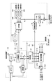
- FIG. 1 is a block diagram showing an overall configuration of a communication device 1 equipped with an RFIC (semiconductor device) 10 according to a first embodiment of the present invention.
- FIG. 2 is a block diagram showing a configuration of a local oscillator 26 in FIG.
- FIG. 3 is a circuit diagram illustrating an example of a configuration of an LC oscillator 50 in FIG. 2. It is a figure which shows an example of a structure of the capacity
- FIG. 5 is a diagram illustrating a relationship between a control voltage and a capacitance value in the voltage control capacitor 102 of FIG. 4.
- FIG. 4 is a diagram illustrating another configuration example of the capacity units 53 and 54 illustrated in FIG. 3.
- FIG. 4 is a diagram showing a change in oscillation frequency when the current adjustment code IC is switched in the LC oscillator 50 in FIG. 3 (when the oscillation frequency is not adjusted by the capacitor 54).
- FIG. 4 is a diagram showing a change in oscillation frequency when the current adjustment code IC is switched in the LC oscillator 50 of FIG. 3 (when the oscillation frequency is adjusted by the capacitor 54).
- It is a block diagram which shows the part relevant to preparation of a table among the local oscillators 26 and the control part 12 of FIG.
- FIG. 6 is a timing chart showing the state of switching units SW1 and SW2, the time change of the values of control codes IC and CN, and the time change of the oscillation frequency during calibration.
- FIG. 7 is a timing chart showing the states of switching units SW1 and SW2, time changes in values of control codes IC and CN, and time changes in oscillation frequency during normal operation.
- It is a block diagram which shows the structure of 26 A of local oscillators and the control part 12 by Embodiment 2 of this invention.
- It is a figure which shows notionally an example of a structure of the digital low-pass filter 62A of FIG.
- It is a figure for demonstrating the relationship between the pass-band width of a digital low-pass filter, and lockup time.
- It is a figure for demonstrating the phase noise characteristic of a PLL circuit.
- It is a block diagram which shows the structure of the local oscillator 26B and the control part 12A by Embodiment 3 of this invention.
- FIG. 50 It is a figure which shows the structure of LC oscillator 50A as a modification of Embodiment 1, and the control part 12B which controls this. It is a figure which shows the structure of LC oscillator 50B and the control part 12C which controls this as a modification of Embodiment 2.
- FIG. It is a figure for demonstrating the suppression method of the oscillation frequency jump more generally.
- FIG. 1 is a block diagram showing an overall configuration of a communication device 1 equipped with an RFIC (semiconductor device) 10 according to Embodiment 1 of the present invention.
- the communication device 1 includes a baseband circuit (BBIC: Baseband IC) 2, an RFIC 10, a converter 3 that converts the impedance of a differential signal and converts the differential signal into a single-ended signal, and a power amplifier (HPA: High (Power Amplifier) 4, a front-end module (FEM) 5, an antenna 6, and a converter 7 that converts a single-end signal into a differential signal and converts the impedance of the differential signal.
- BBIC Baseband IC
- HPA High (Power Amplifier) 4
- FEM front-end module
- T non-inverted signal
- B inverted signal
- the baseband circuit 2 First, at the time of transmission, the baseband circuit 2 generates an I signal and a Q signal that is a quadrature component based on transmission data.
- the generated I signal and Q signal are converted into a serial differential signal S_TX together with a control signal to the RFIC 10, and output to the RFIC 10 by LVDS (Low Voltage Differential Signaling).
- the serial differential signal S_TX is serial-parallel converted by the interface unit 11 of the RFIC 10 and separated into an I signal Di and a Q signal Dq and a control signal to the RFIC 10.
- the RFIC 10 includes a correction value adding unit 21, DACs 22 and 23 (DAC: Digital-to-Analog Converter), LPFs 24 and 25 (LPF: Low Pass Filter), a local oscillator 26, and a phase shifter as a configuration of the transmission device. 27, a quadrature modulator 30, and a TXPGA 31 (PGA: Programmable Gain Amplifier) that controls transmission power.
- the first and second offset correction values are added to the digital I signal Di and Q signal Dq output from the interface unit 11 by the correction value adding unit 21, respectively.
- the offset correction value is for suppressing carrier leak of the quadrature modulator 30.
- the DACs 22 and 23 convert the offset-corrected I signal Di and Q signal Dq into analog differential signals, respectively.
- the analog-converted I signal and Q signal after offset correction pass through the LPFs 24 and 25, respectively, and then are input to the quadrature modulator 30 as differential baseband signals BB_I and BB_Q, respectively.
- the quadrature modulator 30 further receives a local oscillation signal LO_I and a local oscillation signal LO_Q, which are analog differential signals generated by the phase shifter 27 based on the output signal of the local oscillator 26.
- a local oscillation signal LO_I and LO_Q are analog differential signals generated by the phase shifter 27 based on the output signal of the local oscillator 26.
- the phase difference between the local oscillation signals LO_I and LO_Q is 90 degrees, and the phase of LO_Q is delayed from the phase of LO_I.
- the local oscillation signals LO_I and LO_Q may be generated by a 1/2 frequency divider.
- the quadrature modulator 30 multiplies the BB_I signal and the LO_I signal, multiplies the BB_Q signal and the BB_Q signal, and subtracts the multiplication result to generate a transmission signal in the transmission frequency band and output it to the TXPGA 31. To do.
- the power amplifier 4 amplifies the transmission signal output from the converter 3.
- the amplified transmission signal is supplied to the antenna 6 through the front end module 5 and radiated from the antenna 6.
- the front end module 5 is a module including a duplexer that separates a transmission signal and a reception signal, and a switch that switches a connection between the duplexer prepared for each transmission / reception frequency band and the antenna 6.
- the reception signal received by the antenna 6 is input to the converter 7 via the front end module 5.
- the converter 7 converts the received signal, which is a single-ended signal, into a differential signal, performs impedance conversion, and transmits the signal to the RFIC 10.
- the RFIC 10 includes, as a receiving apparatus, an LNA 80 (LNA: Low Noise Amplifier), a quadrature demodulator 81, a local oscillator 82, a phase shifter 83, RXPGAs 84 and 85, LPFs 86 and 87, ADCs 88 and 89 ( ADC: Analog-to-Digital Converter).
- LNA 80 Low Noise Amplifier
- quadrature demodulator 81 a quadrature demodulator
- local oscillator 82 a local oscillator
- a phase shifter 83 a phase shifter 83
- RXPGAs 84 and 85 RXPGAs 84 and 85
- LPFs 86 and 87 local oscillator
- ADCs 88 and 89 ADC: Analog-to-Digital Converter
- the received signal input from the converter 7 is amplified by the LNA 80 and then input to the quadrature demodulator 81.
- the quadrature demodulator 81 receives the local oscillation signal RXLO_I and the local oscillation signal RXLO_Q that are analog differential signals generated by the phase shifter 83 based on the output signal of the local oscillator 82.
- the phase difference between the local oscillation signals RXLO_I and RXLO_Q is 90 degrees, and the phase of RXLO_Q is delayed from the phase of RXLO_I.
- the local oscillation signals RXLO_I and RXLO_Q may be generated by a 1/2 frequency divider.
- the quadrature demodulator 81 generates a baseband I signal by multiplying the reception signal and the local oscillation signal RXLO_I, and generates a baseband Q signal by multiplying the reception signal and the local oscillation signal RXLO_Q.
- the baseband I signal and baseband Q signal generated by the quadrature demodulator 81 are subjected to level adjustment by the RXPGAs 86 and 87 after unnecessary waves are removed by the LPFs 84 and 85, respectively.
- the I and Q signals that have passed through the RXPGAs 86 and 87 are digitally converted by the ADCs 88 and 89, respectively.
- the baseband I signal and the baseband Q signal are converted into a serial differential signal S_RX by the interface unit 11 and output to the baseband circuit 2 by LVDS.
- the baseband circuit 2 demodulates the received signal based on the serial differential signal S_RX including the received I signal and Q signal.
- RFIC 10 further includes a control unit 12.
- the control unit 12 receives a control signal from the baseband circuit 2 separated by the interface unit 11 and controls each element of the above-described transmission device and reception device.
- the control unit 12 outputs a gain adjustment code GC for controlling the gain of the TXPGA 31 and a control code FS, IC, CN for controlling the local oscillator 26.
- FIG. 2 is a block diagram showing the configuration of the local oscillator 26 of FIG. 1 and the configuration of the control unit 12 related to the control of the local oscillator 26. 2 also shows the phase shifter 27, the quadrature modulator 30, and the TXPGA 31 of FIG.
- the local oscillator 26 includes an LC oscillator (digitally controlled oscillator) 50, a divider (DIV) 60, a digital phase comparator (DPFD) 61, and a digital low-pass.
- This is an all-digital PLL circuit including a filter (DLPF: Digital Low Pass Filter) 62.
- the LC oscillator 50 oscillates at a frequency corresponding to the value of the digital output (tracking code TR) of the digital low-pass filter 62.
- the output signal (local oscillation signal LO) of the LC oscillator 50 is a differential signal (0, ⁇ ).
- the phase shifter 27 In response to this differential output signal LO, the phase shifter 27 generates local oscillation signals LO_I (0, ⁇ ) and LO_Q ( ⁇ / 2, 3 ⁇ / 2) having phases different from each other by 90 degrees.
- the detailed configuration of the LC oscillator 50 will be described with reference to FIG.
- the frequency divider 60 outputs a signal obtained by dividing the output signal of the LC oscillator 50 (local oscillation signal LO).
- the digital phase comparator 61 detects, for example, a phase difference between a clock signal CK output from a temperature compensated crystal oscillator (not shown) and an output signal from the frequency divider 60, and the detected phase difference. A phase difference signal corresponding to is output. For example, the digital phase comparator 61 detects the time difference between the rising time (or falling time) of the clock signal CK and the clock signal CK.
- the digital low-pass filter 62 is a digital filter that limits the frequency band of the phase difference signal output from the digital phase comparator 61.
- the digital low-pass filter 62 removes high-frequency noise components from the phase difference signal.
- the above-mentioned LC oscillator 50, frequency divider 60, digital phase comparator 61, and digital low-pass filter 62 constitute a feedback loop.
- feedback is applied until the frequency of the signal output from the frequency divider 60 matches the frequency of the clock signal CK. Locking that the frequencies match in this way is called locking.
- the frequency of the local oscillation signal LO coincides with a value obtained by multiplying the frequency of the clock signal CK by the frequency division ratio.
- control unit 12 includes an adder 41, registers 42, 45A, 45B, and 45C, a logic circuit 43, a comparator 44, and a table storage unit 46.
- the control unit 12 receives power control information (+1: power increase, ⁇ 1: power decrease, 0: power maintenance) from the baseband circuit 2 of FIG.
- the adder 41 adds the power control information and the data held in the register 42.
- the addition result of the adder 41 is overwritten in the register 42.
- the register 42 holds the set value PS of the current output power of the communication device 1.
- the set value PS of the output power is 5-bit digital data.
- the logic circuit 43 converts the set value PS of output power into a gain adjustment code GC and outputs it to the TXPGA 31.
- the output of the TXPGA 31 changes according to the value of the gain adjustment code GC.
- the comparator 44 sets the current output power set value PS held in the register 42 and the comparison values 1, 2, 3 held in the registers 45A, 45B, 45C (for example, comparison value 1 ⁇ comparison value 2 ⁇ By comparing with the comparison value 3), the set value PS of 5-bit output power is converted into a 2-bit current adjustment code IC.
- the value of the drive current supplied to the LC oscillator 50 is adjusted according to the current adjustment code IC.
- the number of bits of the current adjustment code IC is not limited to 2 bits. For example, when the comparison value to be compared with the set value PS of the output power is one, the comparator 44 generates a 1-bit current adjustment code IC.
- the table storage unit 46 stores a value of a cancel code CN set in advance in association with a change in the value of the current adjustment code IC.
- the corresponding cancel code CN is output from the table storage unit 46.
- the capacitance value of the capacitor included in the LC oscillator 50 is adjusted, so that the jump of the oscillation frequency of the LC oscillator 50 is suppressed.
- control unit 12 sets a frequency setting code FS for changing the frequency division ratio of the frequency divider 60 in order to set the oscillation frequency of the local oscillator 26 based on the control signal received from the baseband circuit 2 of FIG. Output.
- the phase comparator 61 and the low-pass filter 62 can be configured by analog circuits.
- the LC oscillator 50 oscillates at a frequency corresponding to the value of the control voltage output from the low pass filter 62.
- a digital control code and an analog control voltage are collectively referred to as a control signal.
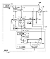
- FIG. 3 is a circuit diagram showing an example of the configuration of the LC oscillator 50 of FIG.
- LC oscillator 50 includes an amplifying unit 201, an LC resonance circuit 202, and a current adjusting unit 56.
- the LC oscillator 50 outputs a differential local oscillation signal LO having an oscillation frequency corresponding to the resonance frequency of the LC resonance circuit 202 from the output nodes ND1 and ND2.
- the amplifying unit 201 includes a pair of NMOS (Negative-channel Metal Oxide Semiconductor) transistors 51 and 52 that are cross-coupled.
- the drain of the NMOS transistor 51 is connected to the first output node ND1, the gate is connected to the second output node ND2, and the source is connected to the connection node ND3.
- the drain of the NMOS transistor 52 is connected to the second output node ND2, the gate is connected to the first output node ND1, and the source is connected to the connection node ND3.
- the LC resonance circuit 202 is connected to the amplification unit 201 as a load of the NMOS transistors 51 and 52.
- the LC resonance circuit 202 includes a capacitor 53, a capacitor 54, and an inductor 55 connected in parallel between the output nodes ND1 and ND2.
- the capacitance value of the capacitance unit 53 changes according to the value of the tracking code TR output from the digital low-pass filter 62 of FIG.
- the capacitance unit 54 is an additional capacitor whose capacitance value changes according to the value of the cancel code CN output from the control unit 12.
- the resonance frequency of the LC resonance circuit 202 is mainly determined by the capacitance value of the capacitor 53 and the inductance value of the inductor 55.
- the midpoint of the inductor 55 is connected to the power supply node VDD.
- the current adjusting unit 56 is connected between the connection node ND3 and the power supply node VSS (ground node).
- the resistance value of the current adjustment unit 56 changes according to the value of the current adjustment code IC output from the control unit 12 of FIG. 2, and accordingly, the drive current (transistor of the amplification unit 201 that flows from the power supply node VDD to the power supply node VSS.
- the collector currents 51 and 52 change.
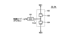
- FIG. 4 is a diagram showing an example of the configuration of the capacity units 53 and 54 shown in FIG.
- each of capacitance units 53 and 54 includes a digital-to-analog converter (DAC) 101 and a voltage control capacitor 102.
- the digital / analog converter 101 converts the control code (tracking code TR or cancel code CN) into an analog control voltage Vcnt.
- the voltage control capacitor 102 includes MOS transistor capacitors (MOSFET Capacitors) 103 and 104 connected in series. The capacitance value of the voltage control capacitor 102 changes according to the control voltage Vcnt applied to the connection node of the MOS transistor capacitors 103 and 104.
- FIG. 5 is a diagram showing the relationship between the control voltage and the capacitance value in the voltage control capacitor 102 of FIG.
- the capacitance value of the voltage control capacitor 102 is determined by the control voltage Vcnt (minimum value VL, maximum value VH) corresponding to the control code.
- FIG. 6 is a diagram showing another configuration example of the capacity units 53 and 54 shown in FIG.
- each of capacitive portions 53 and 54 includes capacitive elements 105 (0) to 105 (m), capacitive elements 106 (0) to 106 (m), and NMOS transistor 107 ( 0) to 107 (m).
- m is an integer determined according to the number of bits of the control code (tracking code TR or cancel code CN).
- the i-th (0 ⁇ i ⁇ m) capacitive element 105 (i), NMOS transistor 107 (i), and capacitive element 106 (i) are connected in series by being connected in series between the output nodes ND1 and ND2. Make up the body.
- Each of the NMOS transistors 107 (0) to 107 (m) is turned on or off in accordance with the value of the control code (tracking code TR, cancel code CN), so that the capacitance values of the capacitance units 53 and 54 change. .
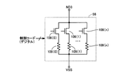
- FIG. 7 is a diagram showing an example of the configuration of the current adjusting unit 56 shown in FIG.
- current adjustment unit 56 includes NMOS transistors 108 (0) to 108 (n) as switching elements and resistance elements 109 (0) to 109 (n).
- n is an integer determined according to the number of bits of the control code (current adjustment code IC).
- the i-th (0 ⁇ i ⁇ n) NMOS transistor 108 (i) and the resistance element 109 (i) are connected in series between the connection node ND3 and the power supply node VSS, thereby forming a series connection body. .
- These n + 1 serially connected bodies are connected in parallel to each other.
- Each of the NMOS transistors 108 (0) to 108 (n) is switched on or off according to the value of the control code (current adjustment code IC), whereby the resistance value of the current adjustment unit 56 changes.
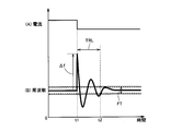
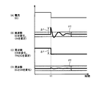
- FIG. 8 is a diagram showing a change in oscillation frequency when the current adjustment code IC is switched in the LC oscillator 50 of FIG.
- the upper graph (A) of FIG. 8 shows the time change of the current flowing through the LC oscillator 50
- the lower graph (B) shows the time change of the oscillation frequency of the LC oscillator 50.
- the drive current flowing through the controlled oscillator is changed by switching the value of the current adjustment code IC at time t1. Due to this change in drive current, a jump of ⁇ f occurs in the oscillation frequency.
- the oscillation frequency returns to the original oscillation frequency by the action of the PLL with the passage of time.
- the time until the oscillation frequency falls within the allowable range FT (from time t1 to time t2) is referred to as a relocking time TRL.
- FIG. 9 is a diagram showing a change in oscillation frequency when the current adjustment code IC is switched in the LC oscillator 50 of FIG.
- the oscillation frequency is adjusted by the capacitor 54 of FIG.
- the graph of (A) shows the time change of the drive current corresponding to the value of the current adjustment code IC.
- the graph of (B) shows the time change of the oscillation frequency when the value of the current adjustment code IC is changed while the cancellation code CN is constant.
- the graph (C) shows the change in the oscillation frequency corresponding to the change in the value of the cancel code CN (the tracking code TR and the current adjustment code IC are constant).
- the graph of (D) shows the time change of the oscillation frequency when both the current adjustment code IC and the value of the cancellation code are changed.
- the drive current flowing through the controlled oscillator is changed by switching the value of the current adjustment code IC at time t1.
- the capacitance value of the capacitor 54 is not adjusted by the cancel code CN, the oscillation frequency jump ⁇ f occurs immediately after time t1, as shown in the graph (B).
- the cancel code CN is switched simultaneously with the switching of the current adjustment code IC at time t1, and thereby, the capacitance unit 54 is configured to cancel the oscillation frequency jump in the graph (B).
- the capacitance value is changed (see graph (C)).
- the jump of the oscillation frequency at time t1 is suppressed, and the oscillation frequency is maintained within the allowable range FT.
- the cancel code CN after the time t1 a value stored in advance in the table storage unit 46 in association with a change in the value of the current adjustment code IC is used.
- a method of creating a table stored in advance in the table storage unit 46 will be described. The table is created during calibration.
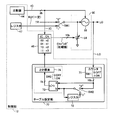
- FIG. 10 is a block diagram showing portions related to the creation of the table in the local oscillator 26 and the control unit 12 in FIG.
- the LC oscillator 50 is shown divided into a capacitor portion 54 and another portion 59.
- local oscillator 26 further includes a switching unit SW1 in addition to the configuration of FIG.
- the control unit 12 further includes a register 47 and a table setting unit 70 in addition to the configuration of FIG.
- the register 47 holds a preset reference code REF.
- REF for example, the median value of the settable range of the tracking code TR is used.
- the table setting unit 70 includes a frequency counter 71, a register 72, a comparator 73, a binary search logic 74, and a switching unit SW2.
- the switching unit SW2 switches whether the frequency counter 71 and the register 72 are connected.
- the register 72 holds the frequency data output from the frequency counter 71.
- the register 72 is connected to the input terminal b of the comparator 73 and outputs the held frequency data to the comparator 73.
- mode 2 the case where the register 72 and the frequency counter 71 are not connected
- the comparator 73 compares the frequency data output from the frequency counter 71 with the frequency data held in the register 72 and outputs the comparison result (1-bit data) to the binary search logic 74 in the operating state. To do. For example, when the value input to the terminal a in FIG. 10 is larger than the value input to the terminal b (a> b), the comparator 73 outputs “1”, and the value input to the terminal a is When the value is less than or equal to the value input to b (a ⁇ b), the comparator 73 outputs “0”.
- the value of the cancel code CN to be supplied after switching is determined by the binary search method.
- the binary search logic 74 sets the initial search range as the entire range from the minimum value to the maximum value of the cancel code CN, and outputs the median value of the search range to the table storage unit 46.
- the median value of the search range is output to the capacity unit 54 of the LC oscillator 50 via the table storage unit 46 and used as the cancel code CN.
- the binary search logic 74 reduces the search range in half. The above process is repeated as many times as the number of bits of the cancel code CN, so that the value of the cancel code CN is finally determined.
- the table storage unit 46 stores the determined value of the cancellation code CN in association with the change in the value of the current adjustment code IC.
- the initial value of the current adjustment code IC is “00”
- the initial value of the cancel code CN is “n0” (n0 means a 10-bit binary number)
- the current A procedure for determining the value of the cancel code CN to be supplied after switching when the adjustment code IC is switched from the initial value “00” to “01” will be described.
- control unit 12 outputs an initial value “00” as current adjustment code IC.
- a constant value reference code REF is input to the LC oscillator 50 instead of the tracking code TR.
- the table setting unit 70 detects the frequency of the local oscillation signal LO output from the LC oscillator 50 and holds it in the register 72.
- control unit 12 outputs a value “01” after switching as current adjustment code IC.
- a constant value reference code REF is input to the LC oscillator 50 instead of the tracking code TR.
- the comparator 73 compares the frequency value of the local oscillation signal LO detected by the frequency counter 71 with the frequency data held in the register 72, and outputs the comparison result to the binary search logic 74. To do.
- the binary search logic 74 reduces the search range by half based on the comparison result of the comparator 73 and outputs the median of the newly set search range to the table storage unit 46.
- the output median value of the search range is given to the capacitance unit 54 of the LC oscillator 50 as a cancel code CN.
- the cancel code CN is 10 bits
- “n1” is determined as the final value of the cancel code CN by repeating the above procedure 10 times.
- the determined value “n1” is stored in the table storage unit 46 in association with the value “01” of the current adjustment code IC after switching.
- “n2” is determined as the value of the cancel code CN supplied after the switching, and is stored by the table storage unit 46.
- “n3” is determined as the value of the cancel code CN supplied after the switching, and stored in the table storage unit 46.
- tracking code TR output from the digital low-pass filter of FIG. 2 is input to LC oscillator 50.
- the frequency counter 71 is in a stopped state (OFF state).
- the cancel code CN output from the table storage unit 46 to the capacity unit 54 in response to this switching is “n0”.
- jumping of the oscillation frequency when switching the current adjustment cord is suppressed.
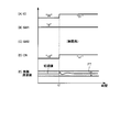
- FIG. 14 is a timing chart showing the state of the switching units SW1 and SW2, the time change of the values of the control codes IC and CN, and the time change of the oscillation frequency during calibration.
- Graph (A) shows the time change of the value of current adjustment code IC
- graph (B) shows the state of switching unit SW1
- graph (C) shows the state of switching unit SW2
- graph (D) shows the cancel code.
- the time variation of the value of CN is shown
- graph (E) shows the time variation of the frequency (oscillation frequency) of the local oscillation signal LO output from the LC oscillator 50.
- the state of switching unit SW1 is “1”.
- the control unit 12 switches the current adjustment code IC from “00” to “01” and switches the state of the switching unit SW2 from “0” to “1” to change the operation mode from mode 1 to mode 2. Transition.
- the control unit 12 adjusts the value of the cancel code CN by the binary search logic 74 so that the oscillation frequency becomes equal to the initial value before the time t1, and finally sets the value of the cancel code CN to “ n1 ".
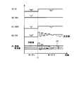
- FIG. 15 is a timing chart showing the state of the switching units SW1 and SW2, the time change of the values of the control codes IC and CN, and the time change of the oscillation frequency during normal operation.
- Graph (A) shows the time change of the value of current adjustment code IC
- graph (B) shows the state of switching unit SW1
- graph (C) shows the state of switching unit SW2
- graph (D) shows the cancel code.
- the time variation of the value of CN is shown
- graph (E) shows the time variation of the frequency (oscillation frequency) of the local oscillation signal LO output from the LC oscillator 50.
- the state of switching unit SW1 is “0” during normal operation, and the state of switching unit SW2 is not related to the operation of control unit 12.
- the control unit 12 switches the value of the current adjustment code IC from “00” to “01”, and switches the value of the cancel code CN from “n0” to “n1”.
- the value of the oscillation frequency can be kept within the allowable range FT with almost no change before and after the time t1.
- the RFIC 10 when the value of the drive current of the LC oscillator 50 is switched by switching the value of the current adjustment code IC, the drive current is changed by adjusting the value of the cancel code CN.
- the amount of oscillation frequency jump before and after the operation can be suppressed. As a result, unlocking can be prevented, and even if unlocking occurs, the time until re-locking can be shortened.
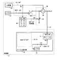
- FIG. 16 is a block diagram showing a configuration of local oscillator 26A and control unit 12 according to the second embodiment of the present invention.
- the local oscillator 26A of FIG. 16 differs from the digital low-pass filter 62 of the first embodiment in the configuration of the digital low-pass filter 62A. Since other local oscillators 26A and control unit 12 are configured in the same manner as in the first embodiment described with reference to FIGS. 2 and 10, the same or corresponding parts are denoted by the same reference numerals. Do not repeat the explanation.
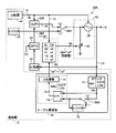
- the digital low-pass filter 62A receives the current adjustment code IC, and increases the pass bandwidth from the normal bandwidth for a predetermined time after the value of the current adjustment code IC is switched. As a result, the jump of the oscillation frequency of the LC oscillator 50 when the current adjustment code IC is switched can be suppressed, and the time (lock-up time) until locking to the desired oscillation frequency can be shortened. Since the digital filter is used, jumping of the oscillation frequency that occurs when the pass bandwidth is returned to the normal bandwidth can be suppressed.
- FIG. 17 is a diagram conceptually illustrating an example of the configuration of the digital low-pass filter 62A in FIG.
- digital low-pass filter 62A includes a calculation unit 110 and a coefficient setting unit 120 that sets a filter coefficient N.
- Arithmetic unit 110 includes multipliers 111 and 112, adders 113 and 114, and delay unit 115.
- the multiplier 111 multiplies the phase difference data PD output from the digital phase comparator 61 of FIG. 16 by 2 ⁇ N (where N is a filter coefficient).
- the adder 113 adds the output of the multiplier 111 and the output of the adder 114 and outputs the result to the delay unit 115.
- the output of the delay device 115 is given as the tracking code TR to the switching unit SW1 in FIG.
- the multiplier 112 multiplies the output of the delay unit 115 by 2 ⁇ N (where N is a filter coefficient). Adder 114 subtracts the output of multiplier 112 from the output of delay unit 115.
- the coefficient setting unit 120 includes exclusive OR (XOR) gates 121 and 122, a logical sum (OR) gate 123, delay circuits 124 and 125, and a determination circuit 126.
- XOR exclusive OR
- the signal IC [1] corresponding to the upper bits is input to the first input terminal of the XOR gate 121 and the delay circuit 124.
- the output of the delay circuit 124 is input to the second input terminal of the XOR gate 121.
- the signal IC [0] corresponding to the lower bits of the current adjustment code IC is input to the first input terminal of the XOR gate 122 and the delay circuit 125.
- the output of the delay circuit 125 is input to the second input terminal of the XOR gate 122.
- the OR gate 123 outputs the logical sum of the outputs of the XOR gates 121 and 122 to the determination circuit 126.
- FIG. 18 is a diagram for explaining the relationship between the passband width of the digital low-pass filter and the lock-up time.
- the graph of A shows the time change of the oscillation frequency when the loop band is widened by making the filter coefficient N relatively small
- the graph of B shows the loop by making the filter coefficient N relatively large.
- the time change of the oscillation frequency when the band is narrowed is shown.
- the lockup time TL1 when the bandwidth is A is shorter than the lockup time TL2 when the bandwidth is B.
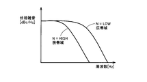
- FIG. 19 is a diagram for explaining the phase noise characteristics of the PLL circuit.
- the horizontal axis represents frequency [Hz]
- the vertical axis represents phase noise [dBc / Hz].
- FIG. 20 is a block diagram showing the configuration of local oscillator 26B and control unit 12A according to the third embodiment of the present invention.
- the local oscillator 26B of FIG. 20 is different from the local oscillator 26A of FIG. 16 in that it does not include the switching unit SW1.
- the tracking code TR is output from the digital low-pass filter 62A to the LC oscillator 50 even during calibration.
- the tracking code TR is input to the comparator 73 provided in the table setting unit 70A and the switching unit SW2.
- the input tracking code TR is held in the register 72.
- mode 2 the input tracking code TR and the tracking code TR held in the register 72 are compared by the comparator 73.
- the binary search logic 74 determines the value of the cancel code CN to be supplied after switching the current adjustment code IC by the binary search method so that the value of the tracking code TR before and after switching the value of the current adjustment code IC becomes equal. To do.
- the binary search logic 74 sets the initial search range as the entire range from the minimum value to the maximum value of the cancel code CN, and outputs the median value of the search range to the table storage unit 46.
- the median value of the search range is output to the capacity unit 54 of the LC oscillator 50 via the table storage unit 46 and used as the cancel code CN.
- the binary search logic 74 reduces the search range in half. The above process is repeated as many times as the number of bits of the cancel code CN, so that the value of the cancel code CN is finally determined.
- the table storage unit 46 stores the determined value of the cancellation code CN in association with the change in the value of the current adjustment code IC.
- the value of the cancel code CN to be output when the 5-bit current adjustment code IC is changed from the initial value “00000” is the value of the current adjustment code IC after the change.
- the value of the cancel code CN to be output when the value of the current adjustment code IC is changed while the oscillation frequency is controlled to a desired value by closed loop control can be determined. it can. Therefore, it is possible to suppress the oscillation frequency jump with higher accuracy than in the first and second embodiments. Since the table is created using the tracking code TR instead of the oscillation frequency, there is an advantage that a frequency counter is not required. Since other points of the third embodiment are the same as those of the first and second embodiments shown in FIGS. 10 and 16, the same or corresponding parts are denoted by the same reference numerals and description thereof will not be repeated.
- the phase comparator 61 and the low-pass filter 62 are digital circuits, but these may be configured by analog circuits. In this case, it is necessary to provide the table setting unit 70A with an analog / digital converter that detects an analog control signal output from the low-pass filter to the LC oscillator, receives the detected analog control signal, and converts it into a digital signal. . The output of the analog / digital converter is input to the comparator 73 and the switching unit SW2.
- FIG. 21 is a diagram illustrating a configuration of an LC oscillator 50A as a modification of the first embodiment and a control unit 12B that controls the LC oscillator 50A.
- the resonant circuit 202A of FIG. 21 is different from the resonant circuit 202 of FIG. 3 in that it further includes a capacitance unit 57 connected between the output nodes ND1 and ND2.
- the capacity value of the capacity unit 57 changes according to the value of the coarse adjustment code CT set in the register 48 in the control unit 12B.
- the oscillation frequency of the LC oscillator 50A can be roughly adjusted by switching the value of the coarse adjustment code CT.
- FIG. 22 is a diagram illustrating a configuration of an LC oscillator 50B and a control unit 12C that controls the LC oscillator 50B as a modification of the second embodiment.
- the configuration of the LC oscillator 50B in FIG. 22 is the same as the configuration of the LC oscillator 50 described in FIG.
- the control unit 12B further includes a register 48 and an adder 49 for holding the coarse adjustment code CT in addition to the configuration shown in FIG.
- the adder 49 adds the coarse adjustment code CT held in the register 48 and the cancel code CN output from the table storage unit 46, and outputs the addition result AD to the capacitor unit 54.
- the capacitance value of the capacitor 54 changes according to the addition result AD. Therefore, the oscillation frequency of the LC oscillator 50A can be roughly adjusted by changing the value of the coarse adjustment code CT.
- the unlocking of the PLL circuit may occur because the load of the LC oscillator fluctuates also by switching the amount of driving current of the frequency divider. Furthermore, when switching transmission / reception in time division duplex (TDD), even if the amplifier amplifier in the transmission output stage is switched on or off, the PLL circuit is unlocked due to voltage fluctuations in the power supply line. May occur.
- TDD time division duplex
- the method for suppressing jumping of the oscillation frequency described in the first to fourth embodiments can be applied to the above case.
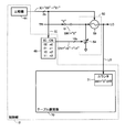
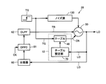
- FIG. 23 is a diagram for explaining a method of suppressing oscillation frequency jump in a more general case.
- the local oscillator (PLL circuit) 26 includes an LC oscillator (controlled oscillator) 50, a frequency divider 60, a digital phase comparator 61, and a digital low-pass filter 62.
- the LC oscillator 50 has the same configuration as that described with reference to FIG. 3, and the oscillation frequency changes according to the tracking code TR output from the digital low-pass filter 62.
- the oscillation frequency of the LC oscillator 50 (frequency of the local oscillation signal LO) jumps when the state of the noise source 130 changes.
- the noise source 130 is, for example, an amplification amplifier at the transmission output stage, and the state change of the noise source 130 (for example, on / off of the amplification amplifier) according to a control signal (referred to as trigger code TG) supplied to the noise source 130 ) Occurs.
- the control unit 12 is a table in which a cancel code CN corresponding to the change in the value is set in advance.
- the capacitance value of the capacitance unit 54 provided in the LC oscillator 50 changes according to the cancel code CN, so that the oscillation frequency jump due to the state change of the noise source 130 does not occur.
- the table stored in advance in the table storage unit 46 can be created by the same method as described in the first embodiment.
- 1 communication device 1 baseband circuit, 4 power amplifier, 10 RFIC (semiconductor device), 11 interface unit, 12, 12A, 12B, 12C control unit, 26, 26A, 26B, 82 local oscillator, 27, 83 phase shifter , 30 quadrature modulator, 46 table storage unit, 50, 50A, 50B LC oscillator, 53, 53, 54, 54, 57 capacitance unit, 55 inductor, 56 current adjustment unit, 60 frequency divider, 61 digital phase comparator, 62, 62A digital low pass filter, 62A digital low pass filter, 70, 70A table setting unit, 71 frequency counter, 74 binary search logic, 81 quadrature demodulator, 201 amplification unit, 202, 202A resonance circuit, CK clock signal, CN cancel Code, CT coarse adjustment code , FS FCW, GC gain adjustment code, IC currents adjustment code, LO local oscillator signal, REF reference code, SW1, SW2 switch unit, TG trigger code, TR tracking code, VDD,
Landscapes
- Engineering & Computer Science (AREA)
- Computer Networks & Wireless Communication (AREA)
- Signal Processing (AREA)
- Stabilization Of Oscillater, Synchronisation, Frequency Synthesizers (AREA)
- Inductance-Capacitance Distribution Constants And Capacitance-Resistance Oscillators (AREA)
Abstract
Description
[通信機1の全体構成]
図1は、この発明の実施の形態1によるRFIC(半導体装置)10を搭載した通信機1の全体構成を示すブロック図である。通信機1は、ベースバンド回路(BBIC:Baseband IC)2と、RFIC10と、差動信号のインピーダンスを変換するとともに差動信号をシングルエンド信号に変換する変換器3と、電力増幅器(HPA:High Power Amplifier)4と、フロントエンドモジュール(FEM:Front-End Module)5と、アンテナ6と、シングルエンド信号を差動信号に変換して、差動信号のインピーダンスを変換する変換器7とを含む。
図2は、図1の局部発振器26の構成と、制御部12のうち局部発振器26の制御に関係する部分の構成を示すブロック図である。図2には、図1の移相器27、直交変調器30、およびTXPGA31も合わせて示される。
図3は、図2のLC発振器50の構成の一例を示す回路図である。図3を参照して、LC発振器50は、増幅部201と、LC共振回路202と、電流調整部56とを含む。LC発振器50は、LC共振回路202の共振周波数に対応した発振周波数を有する差動の局部発振信号LOを出力ノードND1,ND2から出力する。
次に、電流調整コードICが切替わったときにおける発振周波数の跳びの抑制方法について説明する。まず、図3の容量部54によって発振周波数の調整が行なわれない場合、すなわち、発振周波数の跳びが抑制されない場合を説明する。
以下、図11~図15を参照して、電流調整コードICの初期値を“00”、キャンセルコードCNの初期値を“n0”(n0は、10ビットの2進数を意味する)とし、電流調整コードICを初期値“00”から“01”に切替えたとき、切替後に供給すべきキャンセルコードCNの値を決定する手順について説明する。
図16は、この発明の実施の形態2による局部発振器26Aおよび制御部12の構成を示すブロック図である。図16の局部発振器26Aは、デジタルローパスフィルタ62Aの構成が実施の形態1のデジタルローパスフィルタ62と異なる。その他の局部発振器26Aの構成および制御部12の構成は、図2および図10で説明した実施の形態1の場合と同じであるので、同一または相当する部分には同一の参照符号を付して説明を繰返さない。
図20は、この発明の実施の形態3による局部発振器26Bおよび制御部12Aの構成を示すブロック図である。図20の局部発振器26Bは、切替部SW1を含まない点で図16の局部発振器26Aと異なる。実施の形態3の場合には、キャリブレーション時にもデジタルローパスフィルタ62AからLC発振器50にトラッキングコードTRが出力される。
実施の形態4では、図3で説明したLC発振器50の変形例について説明する。
PLL回路のロック外れは、分周器の駆動電流量を切替えることによってもLC発振器の負荷が変動するので生じることがある。さらには、時分割復信(TDD:Time Division Duplex)において送受信の切替を行なうときに、送信出力段の増幅アンプをオンまたはオフに切替えた場合にも、電源ラインの電圧変動によってPLL回路のロック外れが生じることがある。実施の形態1~4で説明した発振周波数の跳びの抑制方法は、上記の場合に対しても適用することができる。
Claims (11)
- 制御発振器(50,50A,50B)を備え、前記制御発振器は、
1または複数のインダクタ(55)および容量値が変更可能な第1の容量部(54)を含む共振回路(202,202A)と、
前記共振回路と接続され、前記共振回路の共振周波数に対応した発振周波数を有する局部発振信号(LO)を出力する増幅部(201)と、
前記増幅部に供給する駆動電流の値を調整する電流調整部(56)とを含み、
前記第1の容量部(54)の容量値および前記電流調整部(56)を制御する制御部(12)をさらに備え、
前記制御部(12)は、前記増幅部(201)に供給する駆動電流の値を変更するように前記電流調整部(56)に指令したときには、前記第1の容量部(54)の容量値も変更する、半導体装置。 - 前記共振回路(202,202A)は、容量値が変更可能な第2の容量部(53)をさらに含み、
前記制御部(12)は、前記第2の容量部(53)の容量値が一定の状態で前記増幅部(201)に供給する駆動電流の値を変更するように前記電流調整部(56)に指令したときには、前記発振周波数を一定に保つように前記第1の容量部(54)の容量値を変更する、請求項1に記載の半導体装置。 - 前記半導体装置は、
前記局部発振信号を分周して出力する分周器(60)と、
前記分周器(60)の出力と与えられた基準信号(CK)との位相差に応じた信号を出力する位相比較器(61)と、
前記位相比較器(61)の出力の高周波成分を除去することによってフィードバック信号(TR)を生成するフィルタ部(62,62A)とをさらに備え、
前記共振回路(50,50A,50B)は、前記フィードバック信号(TR)の値に応じて容量値が変化する第2の容量部(53)をさらに含み、
前記制御部(12,12A,12B,12C)は、前記増幅部(201)に供給する駆動電流の値を変更するように前記電流調整部(56)に指令したときには、前記発振周波数を一定に保つように前記第1の容量部(54)の容量値を変更する、請求項1に記載の半導体装置。 - 与えられたベースバンド信号によって前記局部発振信号(LO)を変調して出力する変調器(30)と、
前記変調器(30)の出力を増幅する、ゲインを調整可能なアンプ(31)とをさらに備える、請求項3に記載の半導体装置。 - 前記制御部は、前記アンプ(31)のゲインに応じて前記増幅部(201)に供給する駆動電流の値を変更するように前記電流調整部(56)に指令する、請求項4に記載の半導体装置。
- 前記半導体装置は、前記フィルタ部(62,62A)と前記制御発振器(50,50A,50B)との間の前記フィードバック信号(TR)の経路に設けられ、前記フィードバック信号(TR)および予め定める一定信号(REF)のいずれか一方を前記制御発振器(50,50A,50B)の前記第2の容量部(53)に供給する切替部(SW1)をさらに含み、
前記第1の容量部(54)の容量値は、前記制御部(12,12B,12C)で生成された第1の制御信号(CN)の値に応じて変化し、
前記電流調整部(56)は、前記制御部(12)で生成された第2の制御信号(IC)の値に応じて前記増幅部(201)に供給する駆動電流の値を調整し、
前記制御部(12,12B,12C)は、キャリブレーション時に、前記切替部(SW1)を切替えることによって前記一定信号(REF)を前記第2の容量部(54)に供給した状態で前記第2の制御信号(IC)の値を変化させ、前記制御部は、前記第2の制御信号(IC)の値を変化させた前後で検出された前記局部発振信号(LO)の周波数が等しくなるように、前記第2の制御信号(IC)の値を変化させた後に供給する前記第1の制御信号(CN)の値を決定し、前記制御部(12)は、決定した前記第1の制御信号(CN)の値を前記第2の制御信号(IC)の値の変化に対応付けてテーブルとして記憶し、
前記制御部(12,12B,12C)は、前記フィードバック信号(TR)が前記切替部(SW1)を介して前記制御発振器(50,50A,50B)に供給される通常動作時において前記第2の制御信号(IC)の値を変化させる場合には、前記第2の制御信号(IC)の値を変化させた後に供給する前記第1の制御信号(CN)の値を前記テーブルに基づいて決定する、請求項3に記載の半導体装置。 - 前記第1の容量部(54)の容量値は、前記制御部(12A,12B,12C)で生成された第1の制御信号(CN)の値に応じて変化し、
前記電流調整部(56)は、前記制御部(12A,12B,12C)で生成された第2の制御信号(IC)の値に応じて前記増幅部(201)に供給する駆動電流の値を調整し、
前記制御部(12A,12B,12C)は、キャリブレーション時に、前記第2の制御信号(IC)の値を変化させ、前記制御部(12A,12B,12C)は、前記第2の制御信号(IC)の値を変化させた前後で検出された前記フィードバック信号(TR)の値が等しくなるように、前記第2の制御信号(IC)の値を変化させた後に供給する前記第1の制御信号(CN)の値を決定し、前記制御部(12A,12B,12C)は、決定した前記第1の制御信号(CN)の値を前記第2の制御信号(IC)の値の変化に対応付けてテーブルとして記憶し、
前記制御部(12A,12B,12C)は、通常動作時に前記第2の制御信号(IC)の値を変化させる場合には、前記第2の制御信号(IC)の値を変化させた後に供給する前記第1の制御信号(CN)の値を前記テーブルに基づいて決定する、請求項3に記載の半導体装置。 - 前記フィルタ部(62A)は、デジタル回路によって構成され、前記制御部(12,12A,12B,12C)からの指令に応じて通過帯域幅を変更可能であり、
前記制御部(12,12A,12B,12C)は、前記増幅部(201)に供給する駆動電流の値を変更するように前記電流調整部(56)に指令したときには、前記フィルタ部(62A)の通過帯域幅を通常の帯域幅よりも増加させる、請求項3に記載の半導体装置。 - 前記半導体装置は、
前記局部発振信号を分周して出力する分周器(60)と、
前記分周器(60)の出力と与えられた基準信号(CK)との位相差に応じた信号を出力する位相比較器(61)と、
前記位相比較器(61)の出力の高周波成分を除去することによってフィードバック信号(TR)を生成するフィルタ部(62,62A)とをさらに備え、
前記共振回路(202A)は、
前記フィードバック信号(TR)の値に応じて容量値が変化する第2の容量部(53)と、
前記制御部(12B)の指令に応じて容量値が変化する第3の容量部(57)とをさらに含み、
前記制御部(12B)は、前記第3の容量部(57)の容量値を一定に保った状態で、前記増幅部(201)に供給する駆動電流の値を変更するように前記電流調整部(56)に指令したときには、前記発振周波数を一定に保つように前記第1の容量部(54)の容量値を変更する、請求項1に記載の半導体装置。 - 前記半導体装置は、
前記局部発振信号を分周して出力する分周器(60)と、
前記分周器(60)の出力と与えられた基準信号(CK)との位相差に応じた信号を出力する位相比較器(61)と、
前記位相比較器(61)の出力の高周波成分を除去することによってフィードバック信号(TR)を生成するフィルタ部(62)とをさらに備え、
前記共振回路(202)は、前記フィードバック信号(TR)の値に応じて容量値が変化する第2の容量部(53)をさらに含み、
前記制御部(12C)は、第1の制御信号(CN)および第2の制御信号(CT)を生成し、
前記第1の容量部(54)の容量値は、前記第1の制御信号(CN)と前記第2の制御信号(CT)とを加算した信号の値に応じて変化し、
前記制御部(12C)は、前記第2の制御信号(CT)を一定に保った状態で、前記増幅部(201)に供給する駆動電流の値を変更するように前記電流調整部(56)に指令したときには、前記発振周波数を一定に保つように前記第1の制御信号(CN)の値を変更する、請求項1に記載の半導体装置。 - 半導体装置であって、制御発振器(50)を備え、
前記制御発振器は、
1または複数のインダクタ(55)、容量値が変更可能な第1の容量部(54)、フィードバック信号(TR)の値に応じて容量値が変化する第2の容量部(53)を含む共振回路(202)と、
前記共振回路(202)と接続され、前記共振回路(202)の共振周波数に対応した発振周波数を有する局部発振信号(LO)を出力する増幅部(201)とを含み、
前記半導体装置は、さらに、
前記局部発振信号(LO)を分周して出力する分周器(60)と、
前記分周器(60)の出力と与えられた基準信号との位相差に応じた信号を出力する位相比較器(61)と、
前記位相比較器(61)の出力の高周波成分を除去することによって前記フィードバック信号(TR)を生成するフィルタ部(62)と、
前記第1の容量部(54)の容量値を制御する制御部(12)とを備え、
前記制御部(12)は、前記発振周波数を変化させるような状態の変化が前記半導体装置に生じたときには、前記発振周波数を一定に保つように前記第1の容量部(54)の容量値を変更する、半導体装置。
Priority Applications (4)
| Application Number | Priority Date | Filing Date | Title |
|---|---|---|---|
| PCT/JP2011/051458 WO2012101774A1 (ja) | 2011-01-26 | 2011-01-26 | 半導体装置 |
| JP2012554564A JP5668082B2 (ja) | 2011-01-26 | 2011-01-26 | 半導体装置 |
| US13/982,249 US9154143B2 (en) | 2011-01-26 | 2011-01-26 | Semiconductor device |
| US14/843,864 US20150381344A1 (en) | 2011-01-26 | 2015-09-02 | Semiconductor device |
Applications Claiming Priority (1)
| Application Number | Priority Date | Filing Date | Title |
|---|---|---|---|
| PCT/JP2011/051458 WO2012101774A1 (ja) | 2011-01-26 | 2011-01-26 | 半導体装置 |
Related Child Applications (2)
| Application Number | Title | Priority Date | Filing Date |
|---|---|---|---|
| US13/982,249 A-371-Of-International US9154143B2 (en) | 2011-01-26 | 2011-01-26 | Semiconductor device |
| US14/843,864 Continuation US20150381344A1 (en) | 2011-01-26 | 2015-09-02 | Semiconductor device |
Publications (1)
| Publication Number | Publication Date |
|---|---|
| WO2012101774A1 true WO2012101774A1 (ja) | 2012-08-02 |
Family
ID=46580381
Family Applications (1)
| Application Number | Title | Priority Date | Filing Date |
|---|---|---|---|
| PCT/JP2011/051458 Ceased WO2012101774A1 (ja) | 2011-01-26 | 2011-01-26 | 半導体装置 |
Country Status (3)
| Country | Link |
|---|---|
| US (2) | US9154143B2 (ja) |
| JP (1) | JP5668082B2 (ja) |
| WO (1) | WO2012101774A1 (ja) |
Cited By (4)
| Publication number | Priority date | Publication date | Assignee | Title |
|---|---|---|---|---|
| JP2014183391A (ja) * | 2013-03-18 | 2014-09-29 | Renesas Electronics Corp | 高周波信号処理装置 |
| JP2017538366A (ja) * | 2014-12-16 | 2017-12-21 | ザイリンクス インコーポレイテッドXilinx Incorporated | MuGFETを含む電圧制御発振器 |
| JP2019004330A (ja) * | 2017-06-15 | 2019-01-10 | ルネサスエレクトロニクス株式会社 | 無線信号処理装置、半導体装置、及び発振周波数変動補正方法 |
| WO2021241268A1 (ja) * | 2020-05-27 | 2021-12-02 | ソニーセミコンダクタソリューションズ株式会社 | Pll回路 |
Families Citing this family (25)
| Publication number | Priority date | Publication date | Assignee | Title |
|---|---|---|---|---|
| US9602113B2 (en) * | 2014-08-27 | 2017-03-21 | Qualcomm Incorporated | Fast frequency throttling and re-locking technique for phase-locked loops |
| WO2016123518A1 (en) * | 2015-01-29 | 2016-08-04 | The Regents Of The University Of California | Switched capacitor dc-to-dc converter and power conversion control methods |
| JP6691287B2 (ja) | 2015-11-18 | 2020-04-28 | 株式会社ソシオネクスト | 電圧制御発振回路及びpll回路 |
| US9762249B1 (en) | 2016-07-29 | 2017-09-12 | Movellus Circuits, Inc. | Reconfigurable phase-locked loop |
| US10158365B2 (en) | 2016-07-29 | 2018-12-18 | Movellus Circuits, Inc. | Digital, reconfigurable frequency and delay generator with phase measurement |
| US9705516B1 (en) * | 2016-07-29 | 2017-07-11 | Movellus Circuits, Inc. | Reconfigurable phase-locked loop with optional LC oscillator capability |
| US9698798B1 (en) * | 2016-07-29 | 2017-07-04 | Movellus Circuits, Inc. | Digital controller for a phase-locked loop |
| US9680480B1 (en) | 2016-07-29 | 2017-06-13 | Movellus Circuits, Inc. | Fractional and reconfigurable digital phase-locked loop |
| US10614182B2 (en) | 2016-10-19 | 2020-04-07 | Movellus Circuits, Inc. | Timing analysis for electronic design automation of parallel multi-state driver circuits |
| US10050634B1 (en) * | 2017-02-10 | 2018-08-14 | Apple Inc. | Quantization noise cancellation for fractional-N phased-locked loop |
| US10740526B2 (en) | 2017-08-11 | 2020-08-11 | Movellus Circuits, Inc. | Integrated circuit design system with automatic timing margin reduction |
| JP7193914B2 (ja) * | 2017-11-17 | 2022-12-21 | ローム株式会社 | 可変遅延回路、pll周波数シンセサイザ、電子機器 |
| WO2019116647A1 (ja) | 2017-12-11 | 2019-06-20 | ソニーセミコンダクタソリューションズ株式会社 | 半導体装置及び無線通信装置 |
| US10594323B2 (en) | 2018-06-13 | 2020-03-17 | Movellus Circuits, Inc. | Locked loop circuit and method with digitally-controlled oscillator (DCO) gain normalization |
| US11496139B2 (en) | 2018-06-13 | 2022-11-08 | Movellus Circuits, Inc. | Frequency measurement circuit with adaptive accuracy |
| US11070215B2 (en) | 2018-06-13 | 2021-07-20 | Movellus Circuits, Inc. | Locked loop circuit and method with digitally-controlled oscillator (DCO) gain normalization |
| US11493950B2 (en) | 2018-06-13 | 2022-11-08 | Movellus Circuits, Inc. | Frequency counter circuit for detecting timing violations |
| KR102681257B1 (ko) * | 2018-12-27 | 2024-07-03 | 에스케이하이닉스 주식회사 | 반도체장치 |
| US11552635B2 (en) * | 2019-05-20 | 2023-01-10 | Cypress Semiconductor Corporation | High performance inductive sensing all digital phase locked loop |
| US10536153B1 (en) * | 2019-06-28 | 2020-01-14 | Dialog Semiconductor B.V. | Signal generator |
| JP7388240B2 (ja) * | 2020-02-27 | 2023-11-29 | セイコーエプソン株式会社 | チャージポンプ回路、pll回路および発振器 |
| US11239849B2 (en) | 2020-04-06 | 2022-02-01 | Movellus Circuits Inc. | Locked loop circuit and method with multi-phase synchronization |
| US12368447B1 (en) | 2022-11-17 | 2025-07-22 | Movellus Circuits Inc. | Clock generator system with dynamic frequency crossover |
| US11831318B1 (en) | 2022-11-17 | 2023-11-28 | Movellus Circuits Inc. | Frequency multiplier system with multi-transition controller |
| US11979165B1 (en) | 2022-11-17 | 2024-05-07 | Movellus Circuits Inc. | Frequency multiplier circuit with programmable frequency transition controller |
Citations (3)
| Publication number | Priority date | Publication date | Assignee | Title |
|---|---|---|---|---|
| JP2009027581A (ja) * | 2007-07-23 | 2009-02-05 | Renesas Technology Corp | 半導体集積回路 |
| JP2009182918A (ja) * | 2008-02-01 | 2009-08-13 | Toyota Industries Corp | 電圧制御発振回路 |
| JP2009201016A (ja) * | 2008-02-25 | 2009-09-03 | Toshiba Corp | 発振器制御装置 |
Family Cites Families (19)
| Publication number | Priority date | Publication date | Assignee | Title |
|---|---|---|---|---|
| JPH0752850B2 (ja) * | 1988-01-19 | 1995-06-05 | 日本電気株式会社 | 送信機 |
| JPH03196706A (ja) | 1989-12-26 | 1991-08-28 | Matsushita Electric Ind Co Ltd | 発振回路 |
| JPH05175858A (ja) * | 1991-12-25 | 1993-07-13 | Japan Radio Co Ltd | Pll回路 |
| US5900785A (en) * | 1996-11-13 | 1999-05-04 | Ericsson Inc. | System and method for offsetting load switching transients in a frequency synthesizer |
| JPH11308285A (ja) * | 1998-04-23 | 1999-11-05 | General Res Of Electronics Inc | Mca用直接変調fsk送信機 |
| JP3434794B2 (ja) | 2000-10-05 | 2003-08-11 | 山形日本電気株式会社 | Pll回路 |
| JP4540247B2 (ja) | 2001-04-13 | 2010-09-08 | 日本テキサス・インスツルメンツ株式会社 | Pll回路 |
| GB0126632D0 (en) | 2001-11-06 | 2002-01-02 | Hitachi Ltd | A communication semiconductor integrated circuit device and a wireless communication system |
| US6838951B1 (en) * | 2002-06-12 | 2005-01-04 | Rf Micro Devices, Inc. | Frequency synthesizer having VCO bias current compensation |
| US20050134336A1 (en) * | 2002-10-31 | 2005-06-23 | Goldblatt Jeremy M. | Adjustable-bias VCO |
| JP2004266571A (ja) * | 2003-02-28 | 2004-09-24 | Nec Electronics Corp | 電圧制御発振器 |
| JP2005109618A (ja) * | 2003-09-29 | 2005-04-21 | Renesas Technology Corp | 通信用半導体集積回路および携帯端末システム |
| JP3840468B2 (ja) | 2003-09-29 | 2006-11-01 | 松下電器産業株式会社 | Pll周波数シンセサイザ |
| EP1583221A1 (en) | 2004-03-31 | 2005-10-05 | NEC Compound Semiconductor Devices, Ltd. | PLL frequency synthesizer circuit and frequency tuning method thereof |
| JP4471849B2 (ja) | 2004-03-31 | 2010-06-02 | Necエレクトロニクス株式会社 | Pll周波数シンセサイザ回路及びその周波数チューニング方法 |
| JP2007074436A (ja) | 2005-09-07 | 2007-03-22 | Asahi Kasei Microsystems Kk | 発振回路 |
| US8073416B2 (en) | 2007-10-25 | 2011-12-06 | Qualcomm Incorporated | Method and apparatus for controlling a bias current of a VCO in a phase-locked loop |
| US8275331B2 (en) * | 2009-04-21 | 2012-09-25 | Qualcomm, Incorporated | PA gain state switching based on waveform linearity |
| JP2010278491A (ja) * | 2009-05-26 | 2010-12-09 | Renesas Electronics Corp | 周波数シンセサイザ |
-
2011
- 2011-01-26 JP JP2012554564A patent/JP5668082B2/ja not_active Expired - Fee Related
- 2011-01-26 WO PCT/JP2011/051458 patent/WO2012101774A1/ja not_active Ceased
- 2011-01-26 US US13/982,249 patent/US9154143B2/en not_active Expired - Fee Related
-
2015
- 2015-09-02 US US14/843,864 patent/US20150381344A1/en not_active Abandoned
Patent Citations (3)
| Publication number | Priority date | Publication date | Assignee | Title |
|---|---|---|---|---|
| JP2009027581A (ja) * | 2007-07-23 | 2009-02-05 | Renesas Technology Corp | 半導体集積回路 |
| JP2009182918A (ja) * | 2008-02-01 | 2009-08-13 | Toyota Industries Corp | 電圧制御発振回路 |
| JP2009201016A (ja) * | 2008-02-25 | 2009-09-03 | Toshiba Corp | 発振器制御装置 |
Non-Patent Citations (1)
| Title |
|---|
| LIANGGE XU ET AL.: "A 2.4-GHz low-power all-digital phase-locked loop", CUSTOM INTEGRATED CIRCUITS CONFERENCE, 2009. CICC '09. IEEE, 13 September 2009 (2009-09-13), pages 331 - 334 * |
Cited By (5)
| Publication number | Priority date | Publication date | Assignee | Title |
|---|---|---|---|---|
| JP2014183391A (ja) * | 2013-03-18 | 2014-09-29 | Renesas Electronics Corp | 高周波信号処理装置 |
| US8963593B2 (en) | 2013-03-18 | 2015-02-24 | Renesas Electronics Corporation | High-frequency signal processing device |
| JP2017538366A (ja) * | 2014-12-16 | 2017-12-21 | ザイリンクス インコーポレイテッドXilinx Incorporated | MuGFETを含む電圧制御発振器 |
| JP2019004330A (ja) * | 2017-06-15 | 2019-01-10 | ルネサスエレクトロニクス株式会社 | 無線信号処理装置、半導体装置、及び発振周波数変動補正方法 |
| WO2021241268A1 (ja) * | 2020-05-27 | 2021-12-02 | ソニーセミコンダクタソリューションズ株式会社 | Pll回路 |
Also Published As
| Publication number | Publication date |
|---|---|
| US20130300477A1 (en) | 2013-11-14 |
| US9154143B2 (en) | 2015-10-06 |
| JP5668082B2 (ja) | 2015-02-12 |
| US20150381344A1 (en) | 2015-12-31 |
| JPWO2012101774A1 (ja) | 2014-06-30 |
Similar Documents
| Publication | Publication Date | Title |
|---|---|---|
| JP5668082B2 (ja) | 半導体装置 | |
| KR101191575B1 (ko) | 프로그램 가능 2점 주파수 합성기 아키텍처, 프로그램 가능 분수 n 분할기, 주파수 합성기 및 주파수 합성기 제어 방법 | |
| KR101344879B1 (ko) | 주파수 튜닝을 위한 오실레이터, 방법 및 컴퓨터-판독가능 저장 매체 | |
| US9344100B2 (en) | Reconfigurable local oscillator for optimal noise performance in a multi-standard transceiver | |
| Vercesi et al. | A dither-less all digital PLL for cellular transmitters | |
| US20160099720A1 (en) | Wideband Digitally Controlled Injection-Locked Oscillator | |
| EP1982410B1 (en) | Oscillator gain equalization | |
| CN102377430B (zh) | 锁相电路和无线电通信设备 | |
| US11411567B2 (en) | Phase interpolation-based fractional-N sampling phase-locked loop | |
| US20100123490A1 (en) | Control circuitry | |
| JP2006080909A (ja) | 位相同期ループ回路 | |
| Lin et al. | Spur minimization techniques for ultra-low-power injection-locked transmitters | |
| US20090206894A1 (en) | Phase-Locked Loop with Adaptive Performance | |
| WO2011002944A1 (en) | Adc-based mixed-mode digital phase-locked loop | |
| Farazian et al. | Fast hopping frequency generation in digital CMOS | |
| US20090243740A1 (en) | Method and system for reduced jitter signal generation | |
| Bruss et al. | A 5-GHz CMOS Type-II PLL With Low $ K_ {\rm VCO} $ and Extended Fine-Tuning Range | |
| JP7857388B2 (ja) | 外部発振器の制御及び較正 | |
| EP3566302B1 (en) | Quadrature oscillator | |
| Cheng et al. | A 2.4-GHz ISM band delta-sigma fractional-n frequency synthesizer with automatic calibration technique | |
| Xu | A Study of Fractional Spur Suppression Techniques in Digital Phase-Locked Loops | |
| WO2024245537A1 (en) | Phase locked loop system and method for tuning oscillator | |
| Soldner | Design of a Delta-sigma fractional-N PLL frequency synthesizer at 1.43 GHz | |
| Lee | Wideband phase-locked loops with high spectral purity for wireless communications | |
| Easwaran et al. | Specification driven design of Phase locked loops |
Legal Events
| Date | Code | Title | Description |
|---|---|---|---|
| 121 | Ep: the epo has been informed by wipo that ep was designated in this application |
Ref document number: 11856983 Country of ref document: EP Kind code of ref document: A1 |
|
| ENP | Entry into the national phase |
Ref document number: 2012554564 Country of ref document: JP Kind code of ref document: A |
|
| NENP | Non-entry into the national phase |
Ref country code: DE |
|
| WWE | Wipo information: entry into national phase |
Ref document number: 13982249 Country of ref document: US |
|
| 122 | Ep: pct application non-entry in european phase |
Ref document number: 11856983 Country of ref document: EP Kind code of ref document: A1 |