WO2012093683A1 - 低分子化合物の分子レジストの蒸着装置 - Google Patents
低分子化合物の分子レジストの蒸着装置 Download PDFInfo
- Publication number
- WO2012093683A1 WO2012093683A1 PCT/JP2012/050079 JP2012050079W WO2012093683A1 WO 2012093683 A1 WO2012093683 A1 WO 2012093683A1 JP 2012050079 W JP2012050079 W JP 2012050079W WO 2012093683 A1 WO2012093683 A1 WO 2012093683A1
- Authority
- WO
- WIPO (PCT)
- Prior art keywords
- film
- substrate
- resist
- vapor
- deposition head
- Prior art date
- Legal status (The legal status is an assumption and is not a legal conclusion. Google has not performed a legal analysis and makes no representation as to the accuracy of the status listed.)
- Ceased
Links
Images




Classifications
-
- H—ELECTRICITY
- H10—SEMICONDUCTOR DEVICES; ELECTRIC SOLID-STATE DEVICES NOT OTHERWISE PROVIDED FOR
- H10P—GENERIC PROCESSES OR APPARATUS FOR THE MANUFACTURE OR TREATMENT OF DEVICES COVERED BY CLASS H10
- H10P72/00—Handling or holding of wafers, substrates or devices during manufacture or treatment thereof
- H10P72/04—Apparatus for manufacture or treatment
- H10P72/0402—Apparatus for fluid treatment
- H10P72/0418—Apparatus for fluid treatment for etching
- H10P72/0421—Apparatus for fluid treatment for etching for drying etching
-
- H—ELECTRICITY
- H10—SEMICONDUCTOR DEVICES; ELECTRIC SOLID-STATE DEVICES NOT OTHERWISE PROVIDED FOR
- H10P—GENERIC PROCESSES OR APPARATUS FOR THE MANUFACTURE OR TREATMENT OF DEVICES COVERED BY CLASS H10
- H10P76/00—Manufacture or treatment of masks on semiconductor bodies, e.g. by lithography or photolithography
- H10P76/20—Manufacture or treatment of masks on semiconductor bodies, e.g. by lithography or photolithography of masks comprising organic materials
- H10P76/204—Manufacture or treatment of masks on semiconductor bodies, e.g. by lithography or photolithography of masks comprising organic materials of organic photoresist masks
- H10P76/2041—Photolithographic processes
-
- G—PHYSICS
- G03—PHOTOGRAPHY; CINEMATOGRAPHY; ANALOGOUS TECHNIQUES USING WAVES OTHER THAN OPTICAL WAVES; ELECTROGRAPHY; HOLOGRAPHY
- G03F—PHOTOMECHANICAL PRODUCTION OF TEXTURED OR PATTERNED SURFACES, e.g. FOR PRINTING, FOR PROCESSING OF SEMICONDUCTOR DEVICES; MATERIALS THEREFOR; ORIGINALS THEREFOR; APPARATUS SPECIALLY ADAPTED THEREFOR
- G03F7/00—Photomechanical, e.g. photolithographic, production of textured or patterned surfaces, e.g. printing surfaces; Materials therefor, e.g. comprising photoresists; Apparatus specially adapted therefor
- G03F7/16—Coating processes; Apparatus therefor
-
- H—ELECTRICITY
- H10—SEMICONDUCTOR DEVICES; ELECTRIC SOLID-STATE DEVICES NOT OTHERWISE PROVIDED FOR
- H10P—GENERIC PROCESSES OR APPARATUS FOR THE MANUFACTURE OR TREATMENT OF DEVICES COVERED BY CLASS H10
- H10P50/00—Etching of wafers, substrates or parts of devices
- H10P50/69—Etching of wafers, substrates or parts of devices using masks for semiconductor materials
- H10P50/691—Etching of wafers, substrates or parts of devices using masks for semiconductor materials for Group V materials or Group III-V materials
- H10P50/692—Etching of wafers, substrates or parts of devices using masks for semiconductor materials for Group V materials or Group III-V materials characterised by their composition, e.g. multilayer masks or materials
-
- H—ELECTRICITY
- H10—SEMICONDUCTOR DEVICES; ELECTRIC SOLID-STATE DEVICES NOT OTHERWISE PROVIDED FOR
- H10P—GENERIC PROCESSES OR APPARATUS FOR THE MANUFACTURE OR TREATMENT OF DEVICES COVERED BY CLASS H10
- H10P50/00—Etching of wafers, substrates or parts of devices
- H10P50/73—Etching of wafers, substrates or parts of devices using masks for insulating materials
-
- H—ELECTRICITY
- H10—SEMICONDUCTOR DEVICES; ELECTRIC SOLID-STATE DEVICES NOT OTHERWISE PROVIDED FOR
- H10P—GENERIC PROCESSES OR APPARATUS FOR THE MANUFACTURE OR TREATMENT OF DEVICES COVERED BY CLASS H10
- H10P72/00—Handling or holding of wafers, substrates or devices during manufacture or treatment thereof
- H10P72/04—Apparatus for manufacture or treatment
- H10P72/0448—Apparatus for applying a liquid, a resin, an ink or the like
-
- H—ELECTRICITY
- H10—SEMICONDUCTOR DEVICES; ELECTRIC SOLID-STATE DEVICES NOT OTHERWISE PROVIDED FOR
- H10P—GENERIC PROCESSES OR APPARATUS FOR THE MANUFACTURE OR TREATMENT OF DEVICES COVERED BY CLASS H10
- H10P72/00—Handling or holding of wafers, substrates or devices during manufacture or treatment thereof
- H10P72/04—Apparatus for manufacture or treatment
- H10P72/0451—Apparatus for manufacturing or treating in a plurality of work-stations
- H10P72/0468—Apparatus for manufacturing or treating in a plurality of work-stations comprising a chamber adapted to a particular process
-
- H—ELECTRICITY
- H10—SEMICONDUCTOR DEVICES; ELECTRIC SOLID-STATE DEVICES NOT OTHERWISE PROVIDED FOR
- H10P—GENERIC PROCESSES OR APPARATUS FOR THE MANUFACTURE OR TREATMENT OF DEVICES COVERED BY CLASS H10
- H10P72/00—Handling or holding of wafers, substrates or devices during manufacture or treatment thereof
- H10P72/04—Apparatus for manufacture or treatment
- H10P72/0451—Apparatus for manufacturing or treating in a plurality of work-stations
- H10P72/0468—Apparatus for manufacturing or treating in a plurality of work-stations comprising a chamber adapted to a particular process
- H10P72/0474—Apparatus for manufacturing or treating in a plurality of work-stations comprising a chamber adapted to a particular process comprising at least one lithography chamber
Definitions
- the present invention relates to a film forming apparatus, a substrate processing system, a substrate processing method, and a semiconductor device manufacturing method for forming a resist film made of a low molecular compound molecular resist on a substrate.
- a resist coating process is performed by applying a resist solution on a semiconductor wafer (hereinafter referred to as “wafer”) to form a resist film, and a predetermined pattern is exposed on the resist film.
- Wafer semiconductor wafer
- An exposure process, a development process for developing the exposed resist film, and the like are sequentially performed to form a predetermined resist pattern on the wafer.
- low molecular resist a low molecular compound molecular resist (hereinafter sometimes referred to as “low molecular resist”) corresponding to an exposure apparatus that outputs light with a short wavelength such as EUV has been proposed (Patent Document 1).
- so-called spin coating is performed in which a resist solution is supplied from a nozzle to the center of a rotating wafer and the resist solution is applied on the wafer by diffusing the resist solution on the wafer by centrifugal force.
- the law is often used.
- the spin coating method when used, it is difficult to uniformly diffuse the resist solution on the wafer, and it is difficult to control the film thickness uniformly, particularly when the resist film is formed in a thin film on the wafer. become.
- low molecular resists are weakly entangled in molecular chains, they are easily crystallized when applied on a wafer. As a result, the LER and LWR of the resist pattern increase.
- the resist solution solvent may remain on the wafer even if the wafer is heat-treated. In such a case, in the subsequent exposure processing, the degree of vacuum in the processing atmosphere deteriorates due to the remaining solvent, and the exposure processing cannot be performed appropriately.
- the present invention has been made in view of such a point, and an object thereof is to appropriately form a resist film made of a low molecular weight molecular resist on a substrate.
- the present invention provides a film forming apparatus for forming a resist film made of a low molecular weight compound molecular resist on a substrate, which is provided in a processing container for accommodating the substrate, and the processing container.
- a low molecular weight compound means the low molecular weight compound whose molecular weight is 2000 or less, for example.
- a resist film can be formed by supplying vapor of the molecular resist onto a substrate in a vacuum atmosphere and depositing the molecular resist on the substrate.
- the thickness of the resist film on the substrate can be adjusted by adjusting the supply amount of the vapor of the molecular resist, and the thickness of the resist film can be made uniform in the substrate plane.
- the vapor is supplied onto the substrate in a vacuum atmosphere, the molecular resist is supplied in an amorphous state. For this reason, even if the molecular resist is a low molecular compound, the molecular resist is difficult to crystallize. Therefore, even if the resist film on the substrate is patterned, LER and LWR of the resist pattern can be suppressed.
- a resist film made of a low molecular weight molecular resist can be appropriately formed on a substrate.
- Another aspect of the present invention is a substrate processing system for forming a resist pattern made of a low molecular weight molecular resist on a substrate, the film forming apparatus for forming a resist film on the substrate, and the film formation An exposure apparatus that exposes the resist film; and a developing apparatus that develops the exposed resist film.
- the film formation apparatus is provided in the processing container and holds the substrate. And a resist film deposition head for supplying the vapor of the molecular resist to the substrate held on the holding table, and a pressure reducing mechanism for reducing the atmosphere in the processing container to a vacuum atmosphere. .
- Another aspect of the present invention is a substrate processing method for forming a resist pattern made of a low molecular weight compound molecular resist on a substrate, the vapor of the molecular resist being supplied onto the substrate in a vacuum atmosphere, A film forming step of depositing a molecular resist on a substrate to form a resist film, a first heat treatment step for heat-treating the resist film, an exposure step for exposing the resist film, and then the step A second heat treatment step for heat-treating the resist film; a development step for developing the resist film; and a third heat treatment step for heat-treating the resist film.
- a method for manufacturing a semiconductor device comprising supplying a vapor of a low molecular compound molecular resist on a substrate in a vacuum atmosphere, and depositing the molecular resist on the substrate to form a resist film
- a first heat treatment step for heat-treating the resist film, an exposure step for exposing the resist film, and a second heat treatment step for heat-treating the resist film is performed.
- a substrate processing method having a development step for developing the resist film and a third heat treatment step for heat-treating the resist film is performed to form a resist pattern made of the molecular resist on the substrate.
- the film to be processed on the substrate is etched using the resist pattern as a mask to manufacture a semiconductor device.
- a resist film made of a low molecular compound molecular resist can be appropriately formed on a substrate.
- (C) shows a state where an antireflection film is formed on the sacrificial film
- (d) shows a state where a resist film is formed on the antireflection film
- (e) shows a state where the resist film is formed.
- a state in which a resist pattern is formed is shown. It is a top view which shows the outline of a structure of the wafer processing system concerning other embodiment. It is a top view which shows the outline of a structure of the wafer processing system concerning other embodiment. It is a longitudinal cross-sectional view which shows the outline of a structure of the film-forming apparatus concerning other embodiment.
- FIG. 1 is a plain view showing an outline of a configuration of a wafer processing system 1 as a substrate processing system according to the present embodiment.
- a photolithography process is performed on a wafer W as a substrate to form a resist pattern on the wafer W.
- a film to be processed for example, a silicon nitride film (SiN) and a silicon oxide film (SiO 2 ) are formed in advance as will be described later.
- the resist used in this embodiment is a so-called chemically amplified resist and has photosensitivity.
- the resist used in this embodiment is a low molecular weight molecular resist having a molecular weight of 2000 or less, more preferably 1000 or less, as will be described later (hereinafter sometimes referred to as “low molecular resist”). It is.
- the wafer processing system 1 carries in / out a plurality of wafers W, for example, between the outside and the wafer processing system 1 in units of cassettes, or loads the wafers W into the cassette C and a main transfer chamber 20 described later. It has a configuration in which a loading / unloading station 2 as a substrate loading / unloading unit for loading / unloading and a processing station 3 including a plurality of processing apparatuses for performing predetermined processing on a wafer W in a single wafer manner are integrally connected. ing.
- the cassette loading table 10 is provided at the loading / unloading station 2.
- the cassette mounting table 10 can mount a plurality of cassettes C in a row in the X direction (vertical direction in FIG. 1). That is, the carry-in / out station 2 is configured to be capable of holding a plurality of wafers W.
- the transfer chamber 11 is adjacent to the cassette mounting table 10 on the Y direction positive direction (right direction in FIG. 1) side.
- the transfer chamber 11 is provided with a wafer transfer body 13 that can move on a transfer path 12 extending in the X direction.
- the wafer carrier 13 can be expanded and contracted in the horizontal direction, and can also move in the vertical direction and around the vertical direction ( ⁇ direction), and the wafer W between the cassette C and load lock chambers 21 and 22 of the processing station 3 described later. Can be transported.
- a main transfer chamber 20 is provided as a substrate transfer unit capable of reducing the pressure inside.
- the main transfer chamber 20 is formed in a substantially polygonal shape (an octagonal shape in the illustrated example) in a plan view, for example, and has a load lock chamber 21 and 22 around it, for example, seven processing devices 23, 24, 25, 26, 27. , 28, 29 are connected.
- the load lock chambers 21, 22 and the processing devices 23, 24, 25, 26, 27, 28, 29 are arranged around the main transfer chamber 20 in this order in the clockwise direction in plan view. .
- each of the gate valves 30 configured to be capable of being provided is provided.
- the main transfer chamber 20 has a transfer chamber chamber 40 having a structure capable of sealing the inside.
- a wafer transfer mechanism 41 that transfers the wafer W is provided in the transfer chamber 40.
- the wafer transfer mechanism 41 has two transfer arms 42 and 42 that hold the wafer W substantially horizontally.
- Each transfer arm 42 is configured to be extendable in the horizontal direction and movable in the vertical direction and the vertical direction ( ⁇ direction).
- the wafer transfer mechanism 41 can transfer the wafer W to the load lock chambers 21 and 22 and the processing apparatuses 23 to 29 around the main transfer chamber 20.
- the load lock chambers 21 and 22 are disposed between the main transfer chamber 20 and the transfer chamber 11 between the carry-in / out station 2 and connect the main transfer chamber 20 and the transfer chamber 11.
- the load lock chambers 21 and 22 have a mounting portion (not shown) for the wafer W, and the chamber can be maintained in a reduced pressure atmosphere.
- the load lock chamber 21 may be referred to as “first load lock chamber 21”
- the load lock chamber 22 may be referred to as “second load lock chamber 22”.
- the processing apparatus 23 is a preprocessing apparatus 23 that cleans the surface of the wafer W (the surface on which the processing target film is formed).
- the pretreatment device 23 for example, the surface of the wafer W is irradiated with ultraviolet rays. Then, organic matter and the like on the wafer W are removed by the ultraviolet rays, and the surface of the wafer W is cleaned.
- the surface of the wafer W may be cleaned by, for example, converting a processing gas such as argon gas into plasma and supplying the plasma to the surface of the wafer W.
- the processing devices 24 and 25 are heat treatment devices 24 and 25 that heat-treat the wafer W.
- the heat treatment apparatuses 24 and 25 include, for example, a hot plate (not shown) for placing and heating the wafer W and a cooling plate (not shown) for placing and cooling the wafer W. Both processes can be performed.
- the heat processing temperature in the heat processing apparatuses 24 and 25 is controlled by the control apparatus 100 mentioned later, for example.
- the processing apparatus 26 is a film forming apparatus 26 that forms a resist film on the wafer W.
- the configuration of the film forming apparatus 26 will be described later.
- the processing device 27 is an exposure device 27 that performs exposure processing on the resist film on the wafer W.
- the exposure device 27 has a light source (not shown) that outputs EUV (wavelength 13 nm to 14 nm).
- EUV wavelength 13 nm to 14 nm.
- the resist film on the wafer W is irradiated with EUV, and a predetermined pattern is selectively exposed on the resist film.
- the processing device 28 is a developing device 28 that develops a resist film on the wafer W.
- a developing solution is supplied to the resist film on the wafer W exposed by the exposure device 27. Then, the resist film is developed by this developer, and a resist pattern is formed on the wafer W.
- the developing device 28 may perform dry development using, for example, a plasma developer instead of the above-described wet development using the developer. That is, the developing process in the developing device 28 may be performed in an air atmosphere or may be performed in a predetermined vacuum atmosphere. Therefore, when the development process is performed in an air atmosphere, the wafer W does not necessarily have to be transferred in a vacuum atmosphere, and the development process may be performed outside the wafer processing system 1.
- the processing apparatus 29 is a dimension measuring apparatus 29 that measures the dimension of the resist pattern on the wafer W.
- the dimension measuring device 29 measures the dimension of the resist pattern by using, for example, a scatterometry method.
- the scatterometry method matches the light intensity distribution in the wafer surface detected by irradiating light to the resist pattern of the wafer W to be measured, and the virtual light intensity distribution stored in advance to obtain the light intensity.
- This is a method for estimating the size of a virtual resist pattern having a suitable distribution as the size of an actual resist pattern. In the present embodiment, for example, the height of the resist pattern is measured as the dimension of the resist pattern.
- the film forming apparatus 26 includes a processing container 50 that accommodates the wafer W and has a structure capable of sealing the inside.
- a loading / unloading port 51 for loading / unloading the wafer W is formed on the side surface of the processing container 50 on the main transfer chamber 20 side.
- the carry-in / out port 51 is provided with the gate valve 30 described above.
- a suction port 52 for reducing the atmosphere inside the processing container 50 to a predetermined vacuum atmosphere is formed on the bottom surface of the processing container 50.
- an intake pipe 54 communicating with a vacuum pump 53 is connected to the intake port 52.
- the intake port 52, the vacuum pump 53, and the intake pipe 54 constitute the decompression mechanism of the present invention.
- a holding table 60 for holding the wafer W horizontally is provided.
- the holding table 60 holds the wafer W by, for example, electrostatic adsorption.
- the wafer W is held on the holding table 60 in a face-up state with the surface on which the processing target film is formed facing upward.
- a drive unit 61 incorporating a motor or the like is provided below the holding base 60.
- the drive unit 61 is provided on the bottom surface of the processing container 50 and is attached to a rail 62 that extends along the Y direction.
- the driving unit 61 the holding table 60 moves along the rail 62 and can transfer the wafer W.
- the Y direction in which the rail 62 extends is the transfer direction L of the wafer W.
- the drive part 61 and the rail 62 comprise the conveyance mechanism of this invention.
- Three vapor deposition heads 70, 71, 72 are arranged in this order in the transfer direction L of the wafer W on the ceiling surface of the processing vessel 50.
- the vapor deposition head 70 uses a carrier gas to form a film forming material (hereinafter also referred to as “sacrificial film material”) that forms a sacrificial film that serves as a mask when etching a film to be processed on the wafer W.
- a sacrificial film deposition head 70 for supplying vapor onto the film to be processed.
- the sacrificial film material a material that is a low molecular weight compound that can be supplied from the sacrificial film deposition head 70 onto the wafer W and that can ensure a good etching selectivity with respect to the film to be processed is used.
- a molecular compound having a benzene ring is used.
- the resist film formed by the film formation apparatus 26 is thin, if the resist pattern formed on the resist film is used as a mask, the film to be processed may not be etched appropriately. is there. Therefore, a sacrificial film is separately formed in the present embodiment in order to complement the resist pattern and use it as a mask for the film to be processed.
- a vapor supply source 73 that supplies vapor of the sacrificial film material to the sacrificial film vapor deposition head 70 is connected to the sacrificial film vapor deposition head 70 via a vapor supply pipe 74.
- the steam supply pipe 74 is provided with a supply device group 75 including a valve for controlling the flow of steam of the sacrificial film material, a supply amount adjusting unit, and the like.
- the vapor supply source 73 is connected to a carrier gas supply pipe 73 a for supplying a carrier gas into the vapor supply source 73.
- an inert gas is used as the carrier gas.
- the carrier gas supplied from the carrier gas supply pipe 73a into the vapor supply source 73 is uniformly mixed with the vapor of the sacrificial film material at a predetermined concentration. Further, the vapor of the sacrificial film material is supplied to the sacrificial film deposition head 70 by the carrier gas, and further supplied from the sacrificial film deposition head 70 onto the film to be processed.
- the vapor deposition head 71 uses a carrier gas to vaporize a film forming material (hereinafter, also referred to as “antireflection film material”) that forms an antireflection film for preventing reflection of light during exposure processing.
- a deposition head 71 for an antireflective film for supplying the film onto the sacrificial film.
- a vapor supply source 76 that supplies vapor of the antireflection film material to the antireflection film vapor deposition head 71 is connected to the antireflection film vapor deposition head 71 via a vapor supply pipe 77.
- the steam supply pipe 77 is provided with a supply device group 78 including a valve for controlling the steam flow of the antireflection film material, a supply amount adjusting unit, and the like.
- the vapor supply source 76 is connected to a carrier gas supply pipe 76 a for supplying a carrier gas into the vapor supply source 76.
- a carrier gas supply pipe 76 a for supplying a carrier gas into the vapor supply source 76.
- an inert gas is used as the carrier gas.
- the carrier gas supplied from the carrier gas supply pipe 76a into the vapor supply source 76 is uniformly mixed with the vapor of the antireflection film material at a predetermined concentration. Further, the vapor of the antireflection film material is supplied to the antireflection film deposition head 71 by the carrier gas, and further supplied from the antireflection film deposition head 71 onto the sacrificial film.
- the vapor deposition head 72 is a resist film vapor deposition head 72 that supplies a low molecular resist vapor onto the antireflection film using a carrier gas.
- the low molecular weight resist is, for example, a low molecular weight compound having a molecular weight of 2000 or less, more preferably a molecular weight of 1000 or less.
- a vapor supply source 79 that supplies vapor of low molecular resist to the resist film vapor deposition head 72 is connected to the resist film vapor deposition head 72 via a vapor supply pipe 80.
- the vapor supply pipe 80 is provided with a supply device group 81 including a valve for controlling the flow of the low molecular resist vapor, a supply amount adjusting unit, and the like.
- the vapor supply source 79 is connected to a carrier gas supply pipe 79 a for supplying a carrier gas into the vapor supply source 79.
- a carrier gas supply pipe 79 a for supplying a carrier gas into the vapor supply source 79.
- an inert gas is used as the carrier gas.
- the carrier gas supplied from the carrier gas supply pipe 79a into the vapor supply source 79 is uniformly mixed with the vapor of the low molecular resist at a predetermined concentration. Further, the vapor of the low molecular resist is supplied to the resist film deposition head 72 by the carrier gas, and further supplied from the resist film deposition head 72 onto the antireflection film.
- the deposition heads 70, 71, 72 have a substantially rectangular parallelepiped shape as shown in FIGS. 2 and 3, and extend in the direction perpendicular to the transfer direction L of the wafer W (X direction in the drawing).
- supply ports 82 for supplying vapors of film forming materials are formed on the wafer W, respectively. .
- Each supply port 82 extends longer than the width in the X direction of the wafer W in the direction perpendicular to the transfer direction L of the wafer W (X direction in the drawing).
- the vapor of the film forming material is uniformly supplied from the vapor heads 70, 71, 72 in the width direction of the wafer W.
- the sacrificial film deposition head 70 is shown in FIG. 3, the antireflection film deposition head 71 and the resist film deposition head 72 have the same configuration.
- the vapor of the sacrificial film material, the vapor of the antireflection film, and the vapor of the low molecular resist are vaporized from the vapor deposition heads 70, 71, 72.
- a sacrificial film, an antireflection film, and a resist film are formed in this order on the film to be processed of the wafer W.
- the vapor deposition heads 70, 71 and 72 supply the vapor of the film forming material using the carrier gas, the vapor of the film forming material is uniformly supplied onto the wafer W.
- the sacrificial film, the antireflection film, and the resist film can be uniformly formed on the film to be processed of the wafer W. Note that by shortening the distance between the vapor deposition heads 70, 71, 72 and the wafer W, the vapor of the film forming material can be used efficiently.
- the sacrificial film on the wafer W is bridged between the sacrificial film vapor deposition head 70 and the antireflection film vapor deposition head 71 on the ceiling surface of the processing vessel 50.
- a first electron beam irradiation unit 90 is provided as a first bridging means for irradiating an electron beam.
- the antireflection film on the wafer W is bridged between the antireflection film deposition head 71 and the resist film deposition head 72, the antireflection film is irradiated with an electron beam as a second bridging means.
- the second electron beam irradiation unit 91 is provided.
- the first electron beam irradiation unit 90 and the second electron beam irradiation unit 91 are each extended longer than the width in the X direction of the wafer W in the direction perpendicular to the transfer direction L of the wafer W (X direction in the drawing). Yes. With this configuration, the electron beams from the first electron beam irradiation unit 90 and the second electron beam irradiation unit 91 are uniformly irradiated in the width direction of the wafer W. In this embodiment, the sacrificial film and the antireflection film are irradiated with the electron beam from the first electron beam irradiation unit 90 and the second electron beam irradiation unit 91, respectively.
- the sacrificial film and the antireflection film may be irradiated with ultraviolet rays, or charged particle beams such as other electron beams may be irradiated.
- the above wafer processing system 1 is provided with a control device 100 as shown in FIG.
- the control device 100 is, for example, a computer and has a program storage unit (not shown).
- the program storage unit stores a program for executing wafer processing in the wafer processing system 1.
- This program is recorded on a computer-readable storage medium H such as a computer-readable hard disk (HD), flexible disk (FD), compact disk (CD), magnetic optical desk (MO), or memory card. May have been installed in the control device 100 from the storage medium H.
- a computer-readable storage medium H such as a computer-readable hard disk (HD), flexible disk (FD), compact disk (CD), magnetic optical desk (MO), or memory card. May have been installed in the control device 100 from the storage medium H.
- FIG. 4 shows the state of the wafer W in the main steps of wafer processing.
- a film F to be processed is formed in advance on the wafer W processed by the wafer processing system 1.
- the film F to be processed is, for example, a silicon nitride film (SiN) and a silicon oxide film (SiO 2 ).
- the wafer W is taken out from the cassette C on the cassette mounting table 10 of the loading / unloading station 2 by the wafer transfer body 13 and transferred to the first load lock chamber 21. Thereafter, the gate valve 30 on the loading / unloading station 2 side of the first load lock chamber 21 is closed. Then, the inside of the first load lock chamber 21 is evacuated, and the inside is decompressed to a predetermined vacuum atmosphere.
- the gate valve 30 between the main transfer chamber 20 and the first load lock chamber 21 is opened, and the wafer W in the first load lock chamber 21 is transferred to the main transfer chamber 20 by the wafer transfer mechanism 41.
- the atmosphere in the main transfer chamber 20 is maintained at a predetermined vacuum atmosphere.
- the gate valve 30 between the main transfer chamber 20 and the first load lock chamber 21 is closed. Thereafter, a predetermined process is performed on the wafer W in each of the processing apparatuses 23 to 29, and the transfer of the wafer W to the processing apparatuses 23 to 29 is performed by the wafer transfer mechanism 41.
- the gate valve 30 is opened and closed each time the wafer transfer mechanism 41 loads and unloads the wafer W with respect to the processing apparatuses 23 to 29. In the following, description of opening and closing of the gate valve 30 between the main transfer chamber 20 and each of the processing apparatuses 23 to 29 is omitted.
- the wafer W in the main transfer chamber 20 is transferred to the pretreatment apparatus 23 by the wafer transfer mechanism 41.
- the surface of the wafer W is irradiated with ultraviolet rays. Then, organic substances and the like on the wafer W, that is, the film F to be processed of the wafer W are removed, and the surface of the wafer W is cleaned.
- the wafer W in the pretreatment apparatus 23 is transferred to the film forming apparatus 26 through the main transfer chamber 20 by the wafer transfer mechanism 41.
- the wafer W transferred to the film forming apparatus 26 is held on the holding table 60 with the surface on which the processing target film F is formed facing upward.
- the wafer W held on the holding table 60 is transferred along the transfer direction L. While the wafer W is processed in the film forming apparatus 26, the atmosphere in the processing container 50 of the film forming apparatus 26 is maintained at a predetermined vacuum atmosphere by the vacuum pump 53.
- the film forming apparatus 26 first, vapor of the sacrificial film material is supplied from the sacrificial film deposition head 70 onto the film F to be processed of the wafer W being transferred. Then, as shown in FIG. 4B, the sacrificial film material is deposited on the film F to be processed, and the sacrificial film H is formed. Subsequently, the sacrificial film H is irradiated with an electron beam from the first electron beam irradiation unit 90, and the sacrificial film material in the sacrificial film H is cross-linked. Thus, the sacrificial film H is appropriately formed on the film F to be processed.
- the vapor of the antireflection film material is supplied from the antireflection film deposition head 71 onto the sacrificial film H of the wafer W. Then, as shown in FIG. 4C, the antireflection film material is deposited on the sacrificial film H to form the antireflection film B. Subsequently, the antireflection film B is irradiated with an electron beam from the second electron beam irradiation unit 91, and the antireflection film material in the antireflection film B is cross-linked. Thus, the antireflection film B is appropriately formed on the sacrificial film H.
- vapor of low molecular resist is supplied from the resist film deposition head 72 onto the antireflection film B of the wafer W. Then, as shown in FIG. 4D, a low molecular resist is deposited on the antireflection film B to form a resist film R.
- the supply amount of the vapor supplied from the vapor deposition heads 70, 71, 72 is such that the film thickness of the sacrificial film H, the film thickness of the antireflection film B, and the film thickness of the resist film R are respectively predetermined. It is adjusted to be a film thickness.
- the wafer transfer mechanism 41 transfers the wafer W in the film forming apparatus 26 to the heat treatment apparatus 24 through the main transfer chamber 20.
- the wafer W is subjected to heat treatment, and so-called pre-baking processing (PAB processing) is performed.
- PAB processing pre-baking processing
- the wafer W in the heat treatment apparatus 24 is transferred to the exposure apparatus 27 through the main transfer chamber 20 by the wafer transfer mechanism 41.
- the resist film R on the wafer W is irradiated with EUV, and a predetermined pattern is selectively exposed on the resist film R.
- the wafer W in the exposure apparatus 27 is transferred to the heat treatment apparatus 25 through the main transfer chamber 20 by the wafer transfer mechanism 41.
- the wafer W is subjected to heat treatment, and so-called post-exposure baking processing (PEB processing) is performed.
- PEB processing post-exposure baking processing
- the wafer W in the heat treatment apparatus 25 is transferred to the developing device 28 through the main transfer chamber 20 by the wafer transfer mechanism 41.
- the developing device 28 a developer is supplied to the exposed resist film R, and the resist film R is developed. In this way, a resist pattern P is formed on the antireflection film B of the wafer W as shown in FIG.
- the wafer W in the developing device 28 is transferred to the heat treatment device 25 through the main transfer chamber 20 by the wafer transfer mechanism 41.
- the wafer W is subjected to heat treatment, and so-called post-baking processing (POST processing) is performed.
- POST processing post-baking processing
- the wafer W in the heat treatment apparatus 25 is transferred by the wafer transfer mechanism 41 to the dimension measuring apparatus 29 through the main transfer chamber 20.
- the height of the resist pattern P on the wafer W is measured by a scatterometry method.
- the measurement result of the dimension measuring device 29 is output to the control device 100.
- the processing conditions of the film forming apparatus 26 are corrected based on the measurement result. Specifically, the temperature and supply amount of the low molecular resist vapor supplied from the resist film deposition head 72 are corrected. Note that only one of the temperature and the supply amount of the vapor of the low molecular resist may be corrected. Thus, the processing conditions of the film forming apparatus 26 are feedback controlled. Then, the subsequent wafer W is processed under the corrected processing conditions, and a resist film R is formed on the wafer W with an appropriate film thickness.
- the wafer W in the dimension measuring device 29 is transferred by the wafer transfer mechanism 41 to the second load lock chamber 22 through the main transfer chamber 20.
- the inside of the second load lock chamber 22 is depressurized to a predetermined vacuum atmosphere.
- the wafer W is transferred by the wafer transfer body 13 to the cassette C on the cassette mounting table 10 of the loading / unloading station 2.
- a series of wafer processing in the wafer processing system 1 is completed.
- the vapor of the low molecular resist is supplied from the resist film vapor deposition head 72 onto the wafer W in a vacuum atmosphere, and the low molecular resist is vapor deposited on the wafer W.
- the resist film R can be formed.
- the film thickness of the resist film R on the wafer W can be adjusted by adjusting the supply amount of the low molecular resist vapor, and the film thickness of the resist film R can be made uniform in the wafer surface. Can do.
- the supply port 82 of the resist vapor deposition head 72 extends longer than the width of the wafer W, the vapor of the low molecular resist is supplied uniformly in the width direction of the wafer W. Therefore, the film thickness of the resist film R can be made more uniform in the wafer plane.
- the vapor of the low molecular resist is supplied onto the wafer W in the vacuum atmosphere in the film forming apparatus 26, the low molecular resist is supplied in an amorphous state. For this reason, even if the molecular resist is a low molecular compound, the low molecular resist is difficult to crystallize. Therefore, LER and LWR of the resist pattern P formed on the wafer W can be suppressed thereafter.
- the film forming apparatus 26 since the low molecular resist vapor supplied onto the wafer W does not contain a solvent for dissolving the molecular resist, the solvent remains on the wafer W as in the prior art. There is no. Therefore, in the subsequent exposure process in the exposure apparatus 27, the degree of vacuum in the processing atmosphere is not deteriorated by the remaining solvent, and the exposure process can be performed appropriately.
- the sacrificial film H, the antireflection film B, and the resist film R are sequentially formed on the film F to be processed of the wafer W.
- the throughput of wafer processing can be improved.
- the sacrificial film H, the antireflection film B, and the resist film R are formed using sacrificial film material vapor, antireflection film material vapor, and low molecular resist vapor, respectively. That is, the solvent for the film forming material is not used to form these films.
- the sacrificial film H, the antireflection film B, and the resist film R can be appropriately stacked without causing the film forming material solvent of one film to damage the other films. Further, the interface between the sacrificial film H, the antireflection film B, and the resist film R can be clearly defined.
- the sacrificial film H and the antireflection film B on the wafer W are irradiated with an electron beam, so that the sacrificial film H and the antireflection film B can be cross-linked. Therefore, the sacrificial film H and the antireflection film B can be appropriately formed.
- the wafer processing system 1 since the wafer processing system 1 includes the film forming apparatus 26 described above, the resist pattern P can be appropriately formed on the wafer W. Further, since the wafer processing system 1 has a configuration in which various processing apparatuses 23 to 29 for performing wafer processing are connected to the main transfer chamber 20, the wafer processing can be performed efficiently.
- the processing conditions of the film forming apparatus 26 are feedback controlled based on the height of the resist pattern P formed on the wafer W in the wafer processing system 1. Can be handled appropriately. As a result, the yield of the semiconductor device as a product can be improved.
- the dimension measuring device 29 measures the height of the resist pattern P on the wafer W, but other dimensions of the resist pattern P may be measured. For example, the line width of the resist pattern P, the sidewall angle of the resist pattern P, the diameter of the contact hole, and the like may be measured. Regardless of the dimension of any resist pattern, the processing conditions of the film forming apparatus 26 can be feedback controlled based on the measurement result.
- the processing conditions of the film forming apparatus 26 are corrected based on the measurement result of the dimension of the resist pattern P in the dimension measuring apparatus 29.
- the processing conditions of the heat treatment apparatuses 24 and 25 The processing conditions of the exposure device 29 may be corrected.
- the treatment conditions of the heat treatment conditions 24 and 25 are, for example, a heat treatment temperature and a heat treatment time of the wafer W.
- the processing conditions of the exposure device 29 are, for example, an exposure amount (a dose amount of light from the exposure light source), a focus value at the time of exposure processing, and the like.
- any one of the processing conditions of the film forming apparatus 26, the processing conditions of the heat treatment apparatuses 24 and 25, and the processing conditions of the exposure apparatus 29 may be corrected, or a plurality of processing conditions may be corrected. May be.
- the wafer processing system 1 has the dimension measuring device 29 that measures the dimension of the resist pattern P on the wafer W, but the film of the resist film R on the wafer W as shown in FIG. You may have the film thickness measuring apparatus 110 which measures thickness.
- the film thickness measuring device 110 is disposed instead of the dimension measuring device 29, but both the dimension measuring device 29 and the film thickness measuring device 110 may be provided in the wafer processing system 1.
- the film thickness measuring apparatus 110 measures the dimension of the resist film R using, for example, an ellipsometry method.
- the ellipsometry method the resist film R of the wafer W to be measured is irradiated with light, the change in the polarization state of incident and reflected when the light is reflected is measured, and the film thickness of the resist film R is determined from the measurement result. This is a calculation method.
- the film thickness of the resist film R is measured by the film thickness measuring apparatus 110.
- the measurement result of the film thickness measuring device 110 is output to the control device 100.
- the processing conditions of the film forming apparatus 26 are corrected based on the measurement result. Specifically, at least the temperature or supply amount of the low molecular resist vapor supplied from the resist film deposition head 72 is corrected. Alternatively, the supply flow rate for transporting the vapor of the low molecular resist may be corrected as a processing condition of the film forming apparatus 26.
- the processing conditions of the film forming apparatus 26 are feedback controlled. Then, the subsequent wafer W is processed under the corrected processing conditions, and a resist film R is formed on the wafer W with an appropriate film thickness.
- the loading / unloading station 2 of the wafer processing system 1 of the above embodiment has loaded and unloaded the wafer W with respect to the processing station 3. However, the loading and unloading portions of the wafer W with respect to the processing station are separated, and the wafer W is loaded. Wafer processing may be performed while transporting in one direction.
- the wafer processing system 200 serves as a substrate carry-in unit that carries a plurality of wafers W into the wafer processing system 200 from the outside or carries a wafer W into a main transfer chamber 210 described later.
- a loading station 201, a processing station 202 including a plurality of processing apparatuses that perform predetermined processing on the wafer W in a single wafer manner, and a plurality of wafers W are unloaded from the wafer processing system 200
- An unloading station 203 as a substrate unloading unit for unloading the wafer W from the transfer chamber 210 is integrally connected in the Y direction.
- the processing station 202 is provided with a main transfer chamber 210 as a substrate transfer unit capable of reducing the pressure inside.
- the main transfer chamber 210 is formed in, for example, a substantially rectangular shape in plan view.
- a first load lock chamber 21 is provided between the main transfer chamber 210 and the carry-in station 201, and a second load lock chamber 22 is provided between the main transfer chamber 210 and the carry-out station 203.
- a pretreatment device 23 On the positive side in the X direction (upward in FIG. 6) of the main transfer chamber 210, a pretreatment device 23, a film formation device 26, an exposure device 27, and a development device 28 are provided in this order from the carry-in station 201 side. It has been.
- On the negative side in the X direction (downward in FIG.
- the main transfer chamber 210 has a transfer chamber chamber 211 having a structure capable of sealing the inside.
- a wafer transfer mechanism 212 for transferring the wafer W is provided in the transfer chamber 211.
- the wafer transfer mechanism 212 has, for example, a transfer arm that can be expanded and contracted in the horizontal direction and movable in the vertical direction and the vertical direction ( ⁇ direction).
- the wafer transfer mechanism 212 can move in the transfer chamber 211 and transfer the wafer W to the load lock chambers 21 and 22 and the processing apparatuses 23 to 29 around the main transfer chamber 20.
- the wafer W is taken out from the cassette C on the cassette mounting table 10 by the wafer transfer body 13 of the carry-in station 201 and transferred to the first load lock chamber 21. Subsequently, the wafer W in the first load lock chamber 21 is transferred into the main transfer chamber 210 by the wafer transfer mechanism 212.
- the wafer W transferred to the main transfer chamber 210 is subjected to a predetermined process in each of the processing apparatuses 23 to 29, and a resist pattern P is formed on the wafer W.
- the predetermined processing in these processing apparatuses 23 to 29 is the same as the wafer processing in the above-described embodiment, and thus description thereof is omitted.
- the wafer W in the main transfer chamber 210 is transferred to the second load lock chamber 22 by the wafer transfer mechanism 212.
- the wafer W is transferred to the cassette C on the cassette mounting table 10 by the wafer transfer body 13 of the unloading station 203.
- a series of wafer processing in the wafer processing system 1 is completed.
- the resist film R can be appropriately formed on the wafer W and the resist pattern P can be appropriately formed, and the same effects as those of the above embodiment can be enjoyed.
- the arrangement and number of processing apparatuses can be arbitrarily set.
- the number of processing devices may be changed according to the processing time required for each processing.
- other processing apparatuses such as a high-accuracy temperature adjusting apparatus that adjusts the temperature of the wafer W under highly accurate temperature management may be arranged.
- the configuration of the film forming apparatus 26 is not limited to the configuration of the above-described embodiment, and any device that deposits a low molecular weight resist in a vacuum atmosphere may be used.
- the film forming apparatus 250 includes a processing container 260 having a structure in which the wafer W is accommodated and the inside can be sealed.
- a loading / unloading port 261 for loading / unloading the wafer W is formed on the side surface of the processing container 260 on the main transfer chamber 20 side.
- the carry-in / out port 261 is provided with the gate valve 30 described above.
- a suction port 262 for reducing the atmosphere inside the processing container 260 to a predetermined vacuum atmosphere is formed on the ceiling surface of the processing container 260.
- an intake pipe 264 communicating with the vacuum pump 263 is connected to the intake port 262.
- a holding table 270 for holding the wafer W horizontally is provided on the ceiling surface in the processing container 260.
- the holding table 270 holds the wafer W by, for example, electrostatic adsorption.
- the wafer W is held on the holding table 270 in a face-down state with the surface on which the processing target film F is formed facing down.
- a so-called point source type vapor deposition head 280 is provided below the holding table 270.
- the vapor deposition head 280 is connected to a vapor supply source 281 that supplies the vapor of the low molecular resist to the vapor deposition head 280 via a vapor supply pipe 282.
- the vapor supply pipe 282 is provided with a supply device group 283 including a valve for controlling the vapor flow of the low molecular resist, a supply amount adjusting unit, and the like.
- the atmosphere in the processing container 260 is maintained in a predetermined vacuum atmosphere by the vacuum pump 263. Thereafter, the vapor of the low molecular resist is supplied from the vapor deposition head 280 to the wafer W. Then, a low molecular resist is deposited on the wafer W to form a resist film R.
- the wafer processing systems 1 and 200 are provided with a reversing mechanism that reverses the front and back surfaces of the wafer W.
- the resist film R is formed on the wafer W in the film forming apparatus 250.
- the resist film R is formed.
- a film forming apparatus having the same configuration as that of the film forming apparatus 250 is separately provided. That is, a film forming apparatus for forming the sacrificial film H and a film forming apparatus for forming the antireflection film B are separately provided.
- the resist pattern P is formed on the wafer W. Thereafter, the processing target film F on the wafer W is etched outside the wafer processing system 1 using the resist pattern P as a mask. Thus, the semiconductor device is manufactured.
- the present invention is not limited to such examples. It is obvious for those skilled in the art that various changes or modifications can be conceived within the scope of the idea described in the claims, and these naturally belong to the technical scope of the present invention. It is understood.
- the present invention is not limited to this example and can take various forms.
- the present invention can also be applied to a case where the substrate is another substrate such as an FPD (flat panel display) other than a wafer or a mask reticle for a photomask.
- FPD flat panel display
Landscapes
- Physics & Mathematics (AREA)
- General Physics & Mathematics (AREA)
- Exposure Of Semiconductors, Excluding Electron Or Ion Beam Exposure (AREA)
- Exposure And Positioning Against Photoresist Photosensitive Materials (AREA)
- Physical Vapour Deposition (AREA)
Abstract
基板上に低分子化合物の分子レジストからなるレジストパターンを形成する基板処理システムは、基板上にレジスト膜を成膜する成膜装置と、前記成膜されたレジスト膜を露光する露光装置と、前記露光されたレジスト膜を現像する現像装置と、を備える。前記成膜装置は、基板を収容する処理容器と、前記処理容器内に設けられ、基板を保持する保持台と、前記保持台に保持された基板に対して、前記分子レジストの蒸気を供給するレジスト膜用蒸着ヘッドと、前記処理容器内の雰囲気を真空雰囲気に減圧する減圧機構と、を有する。
Description
本発明は、基板上に低分子化合物の分子レジストからなるレジスト膜を成膜する成膜装置、基板処理システム、基板処理方法及び半導体装置の製造方法に関する。
例えば半導体装置の製造プロセスにおけるフォトリソグラフィー工程では、例えば半導体ウェハ(以下、「ウェハ」という。)上にレジスト液を塗布しレジスト膜を形成するレジスト塗布処理、当該レジスト膜に所定のパターンを露光する露光処理、露光されたレジスト膜を現像する現像処理などが順次行われ、ウェハ上に所定のレジストパターンが形成される。
上述したレジストパターンを形成する際、半導体装置のさらなる高集積化を図るため、近年、当該レジストパターンの微細化が求められている。このため、露光処理に用いられる光を短波長化することが進められている。具体的には、従来、露光光源として例えばKrFレーザ(波長248nm)やArFレーザ(波長193nm)、F2レーザ(波長157nm)などを出力する光源を用いていたが、これらレーザよりさらに短波長、例えば13nm~14nmの極紫外線(EUV;Extreme Ultra Violet)を出力する光源を用いることが検討されている。
しかしながら、レジスト塗布処理を容易に行うという観点から、従来より、レジスト液中の分子レジストには高分子化合物が用いられていた。この高分子化合物は分子サイズが大きく、分子鎖の絡まり合いが強いため、露光処理工程において微細なパターン通りに解像し難い。この結果、特にレジストパターンのLER(Line Edge Roughness)やLWR(Line Width Roughness)が増大する。
そこで、例えばEUVなどの短波長の光を出力する露光装置に対応した、低分子化合物の分子レジスト(以下、「低分子レジスト」という場合がある。)が提案されている(特許文献1)。
ところで、上述したレジスト塗布処理では、回転中のウェハの中心部にノズルからレジスト液を供給し、遠心力によりウェハ上でレジスト液を拡散することよってウェハ上にレジスト液を塗布する、いわゆるスピン塗布法が多く用いられている。
しかしながら、このスピン塗布法を用いて、特許文献1の低分子レジストを溶媒に溶解させたレジスト液をウェハ上に塗布する場合、下記のような懸念がある。
すなわち、スピン塗布法を用いた場合、ウェハ上でレジスト液を均一に拡散させるのが困難であり、特にウェハ上にレジスト膜を薄膜状に形成する場合、膜厚を均一に制御することが困難になる。また、低分子レジストは分子鎖の絡まり合いが弱いため、ウェハ上に塗布すると結晶化し易い。この結果、レジストパターンのLERやLWRが増大する。さらに、レジスト液をウェハ上に塗布した後、当該ウェハを熱処理しても、ウェハ上にレジスト液の溶媒が残存する場合がある。かかる場合、後続の露光処理において、残った溶媒によって処理雰囲気の真空度が悪化して、露光処理を適切に行うことができない。
本発明は、かかる点に鑑みてなされたものであり、基板上に低分子化合物の分子レジストからなるレジスト膜を適切に成膜することを目的とする。
前記の目的を達成するため、本発明は、基板上に低分子化合物の分子レジストからなるレジスト膜を成膜する成膜装置であって、基板を収容する処理容器と、前記処理容器内に設けられ、基板を保持する保持台と、前記保持台に保持された基板に対して、前記分子レジストの蒸気を供給するレジスト膜用蒸着ヘッドと、前記処理容器内の雰囲気を真空雰囲気に減圧する減圧機構と、を有する。なお、低分子化合物とは、例えば分子量が2000以下の低分子量の化合物をいう。
本発明によれば、真空雰囲気下で、基板上に前記分子レジストの蒸気を供給し、当該分子レジストを基板上に蒸着させてレジスト膜を成膜することができる。かかる場合、分子レジストの蒸気の供給量を調節することで、基板上のレジスト膜の膜厚を調節することができ、当該レジスト膜の膜厚を基板面内で均一にすることができる。また、真空雰囲気下で基板上に蒸気を供給するので、分子レジストがアモルファス状態で供給される。このため、分子レジストが低分子化合物であっても、当該分子レジストが結晶化し難い。したがって、基板上のレジスト膜をパターニングしても、レジストパターンのLERやLWRを抑えることができる。さらに、基板上に供給される蒸気には分子レジストを溶解させるための溶媒が含まれていないので、従来のように基板上に溶媒が残存することがない。したがって、後続の露光処理において、残った溶媒によって処理雰囲気の真空度が悪化することがなく、当該露光処理を適切に行うことができる。以上のように本発明によれば、基板上に低分子化合物の分子レジストからなるレジスト膜を適切に成膜することができる。
別な観点による本発明は、基板上に低分子化合物の分子レジストからなるレジストパターンを形成する基板処理システムであって、基板上にレジスト膜を成膜する成膜装置と、前記成膜されたレジスト膜を露光する露光装置と、前記露光されたレジスト膜を現像する現像装置と、を備え、前記成膜装置は、基板を収容する処理容器と、前記処理容器内に設けられ、基板を保持する保持台と、前記保持台に保持された基板に対して、前記分子レジストの蒸気を供給するレジスト膜用蒸着ヘッドと、前記処理容器内の雰囲気を真空雰囲気に減圧する減圧機構と、を有する。
また別な観点による本発明は、基板上に低分子化合物の分子レジストからなるレジストパターンを形成する基板処理方法であって、真空雰囲気下で、基板上に前記分子レジストの蒸気を供給し、当該分子レジストを基板上に蒸着させてレジスト膜を成膜する成膜工程と、その後、前記レジスト膜を熱処理する第1の熱処理工程と、その後、前記レジスト膜を露光する露光工程と、その後、前記レジスト膜を熱処理する第2の熱処理工程と、その後、前記レジスト膜を現像する現像工程と、その後、前記レジスト膜を熱処理する第3の熱処理工程と、を有する。
さらに別な観点による本発明は、半導体装置の製造方法であって、真空雰囲気下で、基板上に低分子化合物の分子レジストの蒸気を供給し、当該分子レジストを基板上に蒸着させてレジスト膜を成膜する成膜工程と、その後、前記レジスト膜を熱処理する第1の熱処理工程と、その後、前記レジスト膜を露光する露光工程と、その後、前記レジスト膜を熱処理する第2の熱処理工程と、その後、前記レジスト膜を現像する現像工程と、その後、前記レジスト膜を熱処理する第3の熱処理工程と、を有する基板処理法方法を行って、基板上に前記分子レジストからなるレジストパターンを形成した後、前記レジストパターンをマスクとして基板上の被処理膜をエッチングして、半導体装置を製造する。
本発明によれば、基板上に低分子化合物の分子レジストからなるレジスト膜を適切に成膜することができる。
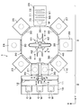
以下、本発明の実施の形態について説明する。図1は本実施の形態にかかる基板処理システムとしてのウェハ処理システム1の構成の概略を示す平明図である。実施の形態のウェハ処理システム1では、基板としてのウェハW上にフォトリソグラフィー処理を行い、ウェハW上にレジストパターンを形成する。また、ウェハ処理システム1で処理されるウェハW上には、後述するように予め被処理膜、例えばシリコン窒化膜(SiN)とシリコン酸化膜(SiO2)が形成されている。
なお、本実施の形態で用いられるレジストは、いわゆる化学増幅型のレジストであって、感光性を有している。また、本実施の形態で用いられるレジストは、後述するように例えば分子量が2000以下、より好ましくは分子量が1000以下の低分子化合物の分子レジスト(以下、「低分子レジスト」という場合がある。)である。
ウェハ処理システム1は、図1に示すように例えば複数のウェハWをカセット単位で外部とウェハ処理システム1との間で搬入出したり、カセットCや後述する主搬送室20に対してウェハWを搬入出したりする基板搬入出部としての搬入出ステーション2と、ウェハWに対して枚葉式に所定の処理を行う複数の処理装置を備えた処理ステーション3とを一体に接続した構成を有している。
搬入出ステーション2には、カセット載置台10が設けられている。カセット載置台10は、複数のカセットCをX方向(図1中の上下方向)に一列に載置自在になっている。すなわち、搬入出ステーション2は、複数のウェハWを保有可能に構成されている。
搬入出ステーション2において、カセット載置台10のY方向正方向(図1中の右方向)側には、搬送室11が隣接されている。搬送室11には、X方向に延伸する搬送路12上を移動可能なウェハ搬送体13が設けられている。ウェハ搬送体13は、水平方向に伸縮自在、且つ鉛直方向及び鉛直周り(θ方向)にも移動自在であり、カセットCと後述する処理ステーション3のロードロック室21、22との間でウェハWを搬送できる。
処理ステーション3の中央部には、内部を減圧可能な基板搬送部としての主搬送室20が設けられている。主搬送室20は、例えば平面視において略多角形状(図示の例では八角形状)に形成され、その周囲にロードロック室21、22と、例えば7つの処理装置23、24、25、26、27、28、29が接続されている。ロードロック室21、22と、処理装置23、24、25、26、27、28、29は、平面視において、主搬送室20の周囲に時計回転方向にこの順で並ぶように配置されている。
搬送室11とロードロック室21、22との間、主搬送室20と各ロードロック室21、22及び各処理装置23~29との間には、これらの間を気密にシールし、かつ開閉可能に構成されたゲートバルブ30がそれぞれ設けられている。
主搬送室20は、内部を密閉可能な構造の搬送室チャンバ40を有している。搬送室チャンバ40内には、ウェハWを搬送するウェハ搬送機構41が設けられている。ウェハ搬送機構41は、ウェハWを略水平に保持する2つの搬送アーム42、42を有している。各搬送アーム42は、水平方向に伸縮自在、且つ鉛直方向及び鉛直周り(θ方向)に移動自在に構成されている。そして、ウェハ搬送機構41は、主搬送室20の周囲のロードロック室21、22及び処理装置23~29に対してウェハWを搬送することができる。
ロードロック室21、22は、主搬送室20と搬入出ステーション2との搬送室11の間に配置され、主搬送室20と搬送室11を接続している。ロードロック室21、22は、ウェハWの載置部(図示せず)を有し、室内を減圧雰囲気に維持できる。なお、以下において、ロードロック室21を「第1のロードロック室21」といい、ロードロック室22を「第2のロードロック室22」という場合がある。
処理装置23は、ウェハWの表面(被処理膜が形成された表面)を洗浄する前処理装置23である。前処理装置23では、例えばウェハWの表面に紫外線を照射する。そして、この紫外線によってウェハW上の有機物等が除去され、当該ウェハWの表面が洗浄される。なお、ウェハWの表面の洗浄は、例えばアルゴンガス等の処理ガスをプラズマ化し、当該プラズマをウェハWの表面に供給して行ってもよい。
処理装置24、25は、ウェハWを熱処理する熱処理装置24、25である。熱処理装置24、25は、例えばウェハWを載置して加熱する熱板(図示せず)と、ウェハWを載置して冷却する冷却板(図示せず)を有し、加熱処理と冷却処理の両方を行うことができる。また、熱処理装置24、25における熱処理温度は、例えば後述する制御装置100により制御される。
処理装置26は、ウェハW上にレジスト膜を成膜する成膜装置26である。成膜装置26の構成については後述する。
処理装置27は、ウェハW上のレジスト膜を露光処理する露光装置27である。露光装置27は、EUV(波長13nm~14nm)を出力する光源(図示せず)を有している。そして、露光装置27では、ウェハW上のレジスト膜にEUVが照射され、当該レジスト膜に所定のパターンが選択的に露光される。
処理装置28は、ウェハW上のレジスト膜を現像処理する現像装置28である。現像装置28では、例えば露光装置27で露光されたウェハW上のレジスト膜に現像液を供給する。そして、この現像液によってレジスト膜が現像され、ウェハW上にレジストパターンが形成される。なお、現像装置28では、上述した現像液によるウェット現像に代えて、例えばプラズマ状の現像液を用いたドライ現像を行ってもよい。すなわち、現像装置28内の現像処理は、大気雰囲気下で行われる場合もあれば、所定の真空雰囲気下で行われる場合もある。したがって、現像処理が大気雰囲気下で行われる場合には、必ずしもウェハWを真空雰囲気下で搬送する必要はなく、当該現像処理をウェハ処理システム1の外部で行ってもよい。
処理装置29は、ウェハW上のレジストパターンの寸法を測定する寸法測定装置29である。寸法測定装置29では、例えばスキャトロメトリ(Scatterometry)法を用いてレジストパターンの寸法を測定する。スキャトロメトリ法は、測定対象のウェハWのレジストパターンに光を照射することで検出されるウェハ面内の光強度分布と、予め記憶されている仮想の光強度分布とをマッチングし、光強度分布が適合した仮想のレジストパターンの寸法を実際のレジストパターンの寸法と推定する方法である。なお、本実施の形態においては、レジストパターンの寸法として、例えばレジストパターンの高さが測定される。
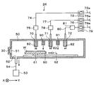
次に、上述した成膜装置26の構成について説明する。成膜装置26は、図2に示すようにウェハWを収容し、内部を密閉可能な構造の処理容器50を有している。処理容器50の主搬送室20側の側面には、ウェハWを搬入出するための搬入出口51が形成されている。搬入出口51には、上述したゲートバルブ30が設けられている。
処理容器50の底面には、当該処理容器50の内部の雰囲気を所定の真空雰囲気まで減圧するための吸気口52が形成されている。吸気口52には、例えば真空ポンプ53に連通する吸気管54が接続されている。なお、本実施の形態においては、吸気口52、真空ポンプ53及び吸気管54が本発明の減圧機構を構成している。
処理容器50の内部には、ウェハWを水平に保持する保持台60が設けられている。保持台60は、例えば静電吸着によってウェハWを保持する。また、ウェハWは、被処理膜が形成された表面を上に向けたフェースアップの状態で保持台60に保持される。保持台60の下方には、例えばモータ等を内蔵した駆動部61が設けられている。駆動部61は、処理容器50の底面に設けられ、Y方向に沿って延伸するレール62に取り付けられている。この駆動部61により、保持台60はレール62に沿って移動し、ウェハWを搬送できる。なお、本実施の形態では、レール62が延伸するY方向がウェハWの搬送方向Lとなる。また、本実施の形態においては、駆動部61とレール62が本発明の搬送機構を構成している。
処理容器50の天井面には、3つの蒸着ヘッド70、71、72が、ウェハWの搬送方向Lにこの順で並べて配置されている。
蒸着ヘッド70は、キャリアガスを用いて、ウェハW上の被処理膜をエッチングする際のマスクとなる犠牲膜を形成する成膜材料(以下、「犠牲膜用材料」という場合がある。)の蒸気を、被処理膜上に供給する犠牲膜用蒸着ヘッド70である。犠牲膜用材料には、犠牲膜用蒸着ヘッド70からウェハW上に供給できる程度に低分子量の化合物であって、且つ被処理膜に対して良好なエッチング選択比を確保できる材料が用いられ、例えばベンゼン環を有する分子化合物が用いられる。なお、本実施の形態では、成膜装置26で成膜されるレジスト膜の膜厚が薄いため、当該レジスト膜に形成されるレジストパターンをマスクとすると、被処理膜を適切にエッチングできない場合がある。このため、レジストパターンを補完して被処理膜のマスクとして用いるために、本実施の形態では犠牲膜を別途形成している。
犠牲膜用蒸着ヘッド70には、当該犠牲膜用蒸着ヘッド70に犠牲膜用材料の蒸気を供給する蒸気供給源73が、蒸気供給管74を介して接続されている。蒸気供給管74には、犠牲膜用材料の蒸気の流れを制御するバルブや供給量調節部等を含む供給機器群75が設けられている。なお、蒸気供給源73には、当該蒸気供給源73内にキャリアガスを供給するためのキャリアガス供給管73aが接続されている。キャリアガスには、例えば不活性ガスが用いられる。そして、キャリアガス供給管73aから蒸気供給源73内に供給されたキャリアガスは犠牲膜用材料の蒸気と所定の濃度で均一に混合される。またこのキャリアガスによって、犠牲膜用材料の蒸気は、犠牲膜用蒸着ヘッド70に供給され、さらに犠牲膜用蒸着ヘッド70から被処理膜上に供給される。
蒸着ヘッド71は、キャリアガスを用いて、露光処理時の光の反射を防止するための反射防止膜を形成する成膜材料(以下、「反射防止膜用材料」という場合がある。)の蒸気を犠牲膜上に供給する反射防止膜用蒸着ヘッド71である。反射防止膜用蒸着ヘッド71には、当該反射防止膜用蒸着ヘッド71に反射防止膜用材料の蒸気を供給する蒸気供給源76が、蒸気供給管77を介して接続されている。蒸気供給管77には、反射防止膜用材料の蒸気の流れを制御するバルブや供給量調節部等を含む供給機器群78が設けられている。なお、蒸気供給源76には、当該蒸気供給源76内にキャリアガスを供給するためのキャリアガス供給管76aが接続されている。キャリアガスには、例えば不活性ガスが用いられる。そして、キャリアガス供給管76aから蒸気供給源76内に供給されたキャリアガスは反射防止膜用材料の蒸気と所定の濃度で均一に混合される。またこのキャリアガスによって、反射防止膜用材料の蒸気は、反射防止膜用蒸着ヘッド71に供給され、さらに反射防止膜用蒸着ヘッド71から犠牲膜上に供給される。
蒸着ヘッド72は、キャリアガスを用いて、低分子レジストの蒸気を反射防止膜上に供給するレジスト膜用蒸着ヘッド72である。低分子レジストは、上述したように例えば分子量が2000以下、より好ましくは分子量が1000以下の低分子量の化合物である。レジスト膜用蒸着ヘッド72には、当該レジスト膜用蒸着ヘッド72に低分子レジストの蒸気を供給する蒸気供給源79が、蒸気供給管80を介して接続されている。蒸気供給管80には、低分子レジストの蒸気の流れを制御するバルブや供給量調節部等を含む供給機器群81が設けられている。なお、蒸気供給源79には、当該蒸気供給源79内にキャリアガスを供給するためのキャリアガス供給管79aが接続されている。キャリアガスには、例えば不活性ガスが用いられる。そして、キャリアガス供給管79aから蒸気供給源79内に供給されたキャリアガスは低分子レジストの蒸気と所定の濃度で均一に混合される。またこのキャリアガスによって、低分子レジストの蒸気は、レジスト膜用蒸着ヘッド72に供給され、さらにレジスト膜用蒸着ヘッド72から反射防止膜上に供給される。
蒸着ヘッド70、71、72は、図2及び図3に示すように略直方体形状を有し、ウェハWの搬送方向Lと垂直方向(図中のX方向)にそれぞれ延伸している。また、蒸着ヘッド70、71、72の下面には、ウェハW上に成膜材料(犠牲膜材料、反射防止膜用材料、低分子レジスト)の蒸気を供給する供給口82がそれぞれ形成されている。各供給口82は、ウェハWの搬送方向Lと垂直方向(図中のX方向)にウェハWのX方向の幅以上に長く延伸している。かかる構成により、蒸気ヘッド70、71、72から成膜材料の蒸気がウェハWの幅方向に均一に供給される。なお、図3では犠牲膜用蒸着ヘッド70を図示したが、反射防止膜用蒸着ヘッド71とレジスト膜用蒸着ヘッド72も同様の構成を有している。
そして、保持台60に保持したウェハWを搬送方向Lに沿って搬送しながら、蒸着ヘッド70、71、72から犠牲膜用材料の蒸気、反射防止膜用材料の蒸気、低分子レジストの蒸気をウェハW上に順次供給することにより、ウェハWの被処理膜上に犠牲膜、反射防止膜、レジスト膜がこの順で成膜される。このとき、蒸着ヘッド70、71、72はキャリアガスを用いて成膜材料の蒸気を供給しているので、当該成膜材料の蒸気はウェハW上に均一に供給される。したがって、ウェハWの被処理膜上に犠牲膜、反射防止膜、レジスト膜をそれぞれ均一に成膜することができる。なお、蒸着ヘッド70、71、72とウェハWとの間の距離を短くすることにより、成膜材料の蒸気を効率よく使用することができる。
処理容器50の天井面には、図2に示すように犠牲膜用蒸着ヘッド70と前記反射防止膜用蒸着ヘッド71との間において、ウェハW上の犠牲膜を架橋させるため、当該犠牲膜に電子ビームを照射する第1の架橋手段としての第1の電子ビーム照射部90が設けられている。また、反射防止膜用蒸着ヘッド71とレジスト膜用蒸着ヘッド72との間には、ウェハW上の反射防止膜を架橋させるため、当該反射防止膜に電子ビームを照射する第2の架橋手段としての第2の電子ビーム照射部91が設けられている。第1の電子ビーム照射部90と第2の電子ビーム照射部91は、それぞれウェハWの搬送方向Lと垂直方向(図中のX方向)にウェハWのX方向の幅以上に長く延伸している。かかる構成により、第1の電子ビーム照射部90及び第2の電子ビーム照射部91からの電子ビームがウェハWの幅方向に均一に照射される。なお、本実施の形態では、第1の電子ビーム照射部90と第2の電子ビーム照射部91からそれぞれ犠牲膜と反射防止膜に電子ビームを照射していたが、犠牲膜と反射防止膜を架橋させることができれば、電子ビーム以外の他の手段を用いることができる。例えば犠牲膜と反射防止膜に対して、紫外線を照射してもよいし、他の電子線等の荷電粒子線などを照射してもよい。
以上のウェハ処理システム1には、図1に示すように制御装置100が設けられている。制御装置100は、例えばコンピュータであり、プログラム格納部(図示せず)を有している。プログラム格納部には、ウェハ処理システム1におけるウェハ処理を実行するプログラムが格納されている。なお、このプログラムは、例えばコンピュータ読み取り可能なハードディスク(HD)、フレキシブルディスク(FD)、コンパクトディスク(CD)、マグネットオプティカルデスク(MO)、メモリーカードなどのコンピュータに読み取り可能な記憶媒体Hに記録されていたものであって、その記憶媒体Hから制御装置100にインストールされたものであってもよい。
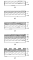
次に、以上のように構成されたウェハ処理システム1で行われるウェハ処理について説明する。図4は、ウェハ処理の主な工程におけるウェハWの状態を示している。なお、図4(a)に示すようにウェハ処理システム1で処理されるウェハW上には、予め被処理膜Fが形成されている。被処理膜Fは、上述したように例えばシリコン窒化膜(SiN)とシリコン酸化膜(SiO2)である。
先ず、ウェハ搬送体13によって、搬入出ステーション2のカセット載置台10上のカセットCからウェハWが取り出され、第1のロードロック室21に搬送される。その後、第1のロードロック室21の搬入出ステーション2側のゲートバルブ30を閉じる。そして、第1のロードロック室21内を排気して、内部を所定の真空雰囲気まで減圧する。
その後、主搬送室20と第1のロードロック室21との間のゲートバルブ30を開き、ウェハ搬送機構41によって第1のロードロック室21内のウェハWが主搬送室20に搬送される。このとき、主搬送室20内の雰囲気は、所定の真空雰囲気に維持されている。
ウェハWが主搬送室20内に搬送されると、主搬送室20と第1のロードロック室21との間のゲートバルブ30を閉じる。なお、その後、各処理装置23~29においてウェハWに所定の処理が行われるが、これら処理装置23~29へのウェハWの搬送はウェハ搬送機構41によって行われる。そして、ウェハ搬送機構41が各処理装置23~29に対してウェハWを搬入出する際には、その都度、ゲートバルブ30の開閉が行われる。以下においては、主搬送室20と各処理装置23~29との間のゲートバルブ30の開閉の説明を省略する。
その後、ウェハ搬送機構41によって、主搬送室20内のウェハWが前処理装置23に搬送される。前処理装置23では、ウェハWの表面に紫外線が照射される。そして、ウェハW上、すなわちウェハWの被処理膜F上の有機物等が除去され、当該ウェハWの表面が洗浄される。
その後、ウェハ搬送機構41によって、前処理装置23内のウェハWが主搬送室20を通って成膜装置26に搬送される。成膜装置26に搬送されたウェハWは、被処理膜Fが形成された表面を上に向けた状態で保持台60に保持される。そして、保持台60に保持されたウェハWは、搬送方向Lに沿って搬送される。なお、成膜装置26においてウェハWを処理する間、当該成膜装置26の処理容器50内の雰囲気は、真空ポンプ53によって所定の真空雰囲気に維持されている。
成膜装置26では、先ず、搬送中のウェハWの被処理膜F上に、犠牲膜用蒸着ヘッド70から犠牲膜用材料の蒸気が供給される。そして、図4(b)に示すように犠牲膜用材料が被処理膜F上に蒸着して犠牲膜Hが形成される。続いて、犠牲膜Hに第1の電子ビーム照射部90から電子ビームが照射され、当該犠牲膜H中の犠牲膜用材料が架橋する。こうして、被処理膜F上に犠牲膜Hが適切に形成される。
続いて、ウェハWの犠牲膜H上に、反射防止膜用蒸着ヘッド71から反射防止膜用材料の蒸気が供給される。そして、図4(c)に示すように反射防止膜用材料が犠牲膜H上に蒸着して反射防止膜Bが形成される。続いて、反射防止膜Bに第2の電子ビーム照射部91から電子ビームが照射され、当該反射防止膜B中の反射防止膜用材料が架橋する。こうして、犠牲膜H上に反射防止膜Bが適切に形成される。
その後、ウェハWの反射防止膜B上に、レジスト膜用蒸着ヘッド72から低分子レジストの蒸気が供給される。そして、図4(d)に示すように低分子レジストが反射防止膜B上に蒸着してレジスト膜Rが形成される。
なお、成膜装置26において、蒸着ヘッド70、71、72から供給される蒸気の供給量は、犠牲膜Hの膜厚、反射防止膜Bの膜厚、レジスト膜Rの膜厚がそれぞれ所定の膜厚になるように調節されている。
ウェハW上にレジスト膜Rが形成されると、ウェハ搬送機構41によって、成膜装置26内のウェハWが主搬送室20を通って熱処理装置24に搬送される。熱処理装置24では、ウェハWが加熱処理され、いわゆるプリベーキング処理(PAB処理)が行われる。
その後、ウェハ搬送機構41によって、熱処理装置24内のウェハWが主搬送室20を通って露光装置27に搬送される。露光装置27では、ウェハW上のレジスト膜RにEUVが照射され、当該レジスト膜Rに所定のパターンが選択的に露光される。
その後、ウェハ搬送機構41によって、露光装置27内のウェハWが主搬送室20を通って熱処理装置25に搬送される。熱処理装置25では、ウェハWが加熱処理され、いわゆるポストエクスポージャーベーキング処理(PEB処理)が行われる。
その後、ウェハ搬送機構41によって、熱処理装置25内のウェハWが主搬送室20を通って現像装置28に搬送される。現像装置28では、露光されたレジスト膜Rに現像液が供給され、当該レジスト膜Rが現像される。こうして、図4(e)に示すようにウェハWの反射防止膜B上にレジストパターンPが形成される。
その後、ウェハ搬送機構41によって、現像装置28内のウェハWが主搬送室20を通って熱処理装置25に搬送される。熱処理装置25では、ウェハWが加熱処理され、いわゆるポストベーキング処理(POST処理)が行われる。
その後、ウェハ搬送機構41によって、熱処理装置25内のウェハWが主搬送室20を通って寸法測定装置29に搬送される。寸法測定装置29では、スキャトロメトリ法によりウェハW上のレジストパターンPの高さが測定される。
寸法測定装置29の測定結果は、制御装置100に出力される。制御装置100では、測定されたレジストパターンPの高さが所望の高さになっていない場合に、当該測定結果に基づいて、成膜装置26の処理条件を補正する。具体的には、レジスト膜用蒸着ヘッド72から供給される低分子レジストの蒸気の温度と供給量が補正される。なお、低分子レジストの蒸気の温度又は供給量のいずれか一方のみを補正してもよい。こうして成膜装置26の処理条件がフィードバック制御される。そして、補正後の処理条件で後続のウェハWが処理されて、当該ウェハW上にレジスト膜Rが適切な膜厚で成膜される。
その後、ウェハ搬送機構41によって、寸法測定装置29内のウェハWが主搬送室20を通って第2のロードロック室22に搬送される。このとき、第2のロードロック室22の内部は、所定の真空雰囲気まで減圧されている。その後、ウェハ搬送体13によって、搬入出ステーション2のカセット載置台10上のカセットCにウェハWが搬送される。こうして、ウェハ処理システム1における一連のウェハ処理が終了する。
以上の実施の形態によれば、成膜装置26において、真空雰囲気下で、レジスト膜用蒸着ヘッド72からウェハW上に低分子レジストの蒸気を供給し、当該低分子レジストをウェハW上に蒸着させてレジスト膜Rを成膜することができる。かかる場合、低分子レジストの蒸気の供給量を調節することで、ウェハW上のレジスト膜Rの膜厚を調節することができ、当該レジスト膜Rの膜厚をウェハ面内で均一にすることができる。また、レジスト用蒸着ヘッド72の供給口82がウェハWの幅以上に長く延伸しているので、低分子レジストの蒸気がウェハWの幅方向に均一に供給される。したがって、レジスト膜Rの膜厚をウェハ面内でより均一にすることができる。
また、成膜装置26において、真空雰囲気下でウェハW上に低分子レジストの蒸気を供給するので、低分子レジストがアモルファス状態で供給される。このため、分子レジストが低分子化合物であっても、当該低分子レジストが結晶化し難い。したがって、その後ウェハW上に形成されるレジストパターンPのLERやLWRを抑えることができる。
さらに、成膜装置26において、ウェハW上に供給される低分子レジストの蒸気には分子レジストを溶解させるための溶媒が含まれていないので、従来のようにウェハW上に溶媒が残存することがない。したがって、後続の露光装置27における露光処理において、残った溶媒によって処理雰囲気の真空度が悪化することがなく、当該露光処理を適切に行うことができる。
また、成膜装置26では、ウェハWの被処理膜F上に犠牲膜H、反射防止膜B、レジスト膜Rが順次形成される。このように一の装置で異なる種類の膜を形成することができるので、ウェハ処理のスループットを向上させることができる。しかも、これら犠牲膜H、反射防止膜B、レジスト膜Rは、それぞれ犠牲膜用材料の蒸気、反射防止膜用材料の蒸気、低分子レジストの蒸気を用いて形成される。すなわち、これらの膜を成膜するために、成膜材料の溶媒が用いられない。したがって、一の膜の成膜材料の溶媒が他の膜にダメージを与えることが無く、犠牲膜H、反射防止膜B、レジスト膜Rを適切に積層することがでる。また、これら犠牲膜H、反射防止膜B、レジスト膜Rの層間の界面も明確にできる。
また、成膜装置26では、ウェハW上の犠牲膜Hと反射防止膜Bに電子ビームを照射するので、これら犠牲膜Hと反射防止膜Bを架橋させることができる。したがって、犠牲膜Hと反射防止膜Bを適切に成膜することができる。
また、ウェハ処理システム1は、上述した成膜装置26を有しているので、ウェハW上にレジストパターンPを適切に形成できる。さらに、ウェハ処理システム1は、ウェハ処理を行う各種処理装置23~29を主搬送室20に接続した構成を有しているので、当該ウェハ処理を効率よく行うことができる。
また、ウェハ処理システム1では、当該ウェハ処理システム1でウェハW上に形成されたレジストパターンPの高さに基づき、成膜装置26の処理条件をフィードバック制御しているので、後続のウェハWを適切に処理することができる。これによって、製品である半導体装置の歩留まりを向上させることができる。
以上の実施の形態では、寸法測定装置29において、ウェハW上のレジストパターンPの高さを測定していたが、レジストパターンPの他の寸法を測定してもよい。例えばレジストパターンPの線幅、レジストパターンPのサイドウォールアングル、コンタクトホールの径などを測定してもよい。いずれのレジストパターンの寸法を測定しても、当該測定結果に基づいて、成膜装置26の処理条件をフィードバック制御できる。
また、以上の実施の形態では、寸法測定装置29におけるレジストパターンPの寸法の測定結果に基づいて、成膜装置26の処理条件を補正していたが、例えば熱処理装置24、25の処理条件や露光装置29の処理条件を補正してもよい。熱処理条件24、25の処理条件とは、例えばウェハWの熱処理温度や熱処理時間等である。また、露光装置29の処理条件とは、例えば露光量(露光光源の光のドーズ量)や露光処理時のフォーカス値等である。また、これら成膜装置26の処理条件、熱処理装置24、25の処理条件、露光装置29の処理条件のうち、いずれか一つの処理条件を補正してもよいし、複数の処理条件を補正してもよい。
以上の実施の形態のウェハ処理システム1は、ウェハW上のレジストパターンPの寸法を測定する寸法測定装置29を有していたが、図5に示すようにウェハW上のレジスト膜Rの膜厚を測定する膜厚測定装置110を有していてもよい。なお、図示の例においては、寸法測定装置29に代えて膜厚測定装置110を配置したが、ウェハ処理システム1内に寸法測定装置29と膜厚測定装置110を両方設けてもよい。
膜厚測定装置110は、例えばエリプソメトリ(Ellipsometry)法を用いてレジスト膜Rの寸法を測定する。エリプソメトリ法は、測定対象のウェハWのレジスト膜Rに光を照射して、光が反射する際の入射と反射の偏光状態の変化を測定し、当該測定結果からレジスト膜Rの膜厚を算出する方法である。
そして、成膜装置26でウェハW上にレジスト膜Rが形成されると、膜厚測定装置110においてレジスト膜Rの膜厚が測定される。この膜厚測定装置110の測定結果は、制御装置100に出力される。制御装置100では、測定されたレジスト膜Rの膜厚が所望の膜厚になっていない場合に、当該測定結果に基づいて、成膜装置26の処理条件を補正する。具体的には、レジスト膜用蒸着ヘッド72から供給される低分子レジストの蒸気の少なくとも温度又は供給量が補正される。あるいは、成膜装置26の処理条件として、低分子レジストの蒸気を搬送するための供給流量を補正してもよい。こうして成膜装置26の処理条件がフィードバック制御される。そして、補正後の処理条件で後続のウェハWが処理されて、当該ウェハW上にレジスト膜Rが適切な膜厚で成膜される。
以上の実施の形態のウェハ処理システム1の搬入出ステーション2は、処理ステーション3に対してウェハWを搬入出していたが、処理ステーションに対するウェハWの搬入部と搬出部を分離し、ウェハWを一方向に搬送しながらウェハ処理を行ってもよい。
かかる場合、図6に示すようにウェハ処理システム200は、複数のウェハWを外部からウェハ処理システム200に搬入したり、後述する主搬送室210にウェハWを搬入したりする基板搬入部としての搬入ステーション201と、ウェハWに対して枚葉式に所定の処理を行う複数の処理装置を備えた処理ステーション202と、複数のウェハWをウェハ処理システム200から外部に搬出したり、後述する主搬送室210からウェハWを搬出したりする基板搬出部としての搬出ステーション203と、をY方向に一体に接続した構成を有している。
搬入ステーション201の構成と搬出ステーション203の構成は、それぞれ上記実施の形態の搬入出ステーション2と同様の構成であるので説明を省略する。
処理ステーション202には、内部を減圧可能な基板搬送部としての主搬送室210が設けられている。主搬送室210は、例えば平面視において略長方形に形成されている。主搬送室210と搬入ステーション201との間には第1のロードロック室21が設けられ、主搬送室210と搬出ステーション203との間には第2のロードロック室22が設けられている。また、主搬送室210のX方向正方向(図6中の上方向)側には、前処理装置23、成膜装置26、露光装置27、現像装置28が搬入ステーション201側からこの順で設けられている。主搬送室210のX方向負方向(図6中の下方向)側には、熱処理装置24、25、25、寸法測定装置29が搬入ステーション201側からこの順で設けられている。搬送室11とロードロック室21、22との間、主搬送室210と各ロードロック室21、22及び各処理装置23~29との間には、これらの間を気密にシールし、かつ開閉可能に構成されたゲートバルブ30がそれぞれ設けられている。なお、これらロードロック室21、22と処理装置23~29の構成は上記実施の形態と同様であるので説明を省略する。
主搬送室210は、内部を密閉可能な構造の搬送室チャンバ211を有している。搬送室チャンバ211内には、ウェハWを搬送するウェハ搬送機構212が設けられている。ウェハ搬送機構212は、例えば水平方向に伸縮自在、且つ鉛直方向及び鉛直周り(θ方向)に移動自在な搬送アームを有している。そして、ウェハ搬送機構212は、搬送室チャンバ211内を移動し、主搬送室20の周囲のロードロック室21、22及び処理装置23~29に対してウェハWを搬送することができる。
以上の構成を有するウェハ処理システム200では、先ず、搬入ステーション201のウェハ搬送体13によって、カセット載置台10上のカセットCからウェハWが取り出され、第1のロードロック室21に搬送される。続いて、ウェハ搬送機構212によって、第1のロードロック室21内のウェハWが主搬送室210内に搬送される。
主搬送室210に搬送されたウェハWには各処理装置23~29において所定の処理が行われ、当該ウェハW上にレジストパターンPが形成される。なお、これら処理装置23~29における所定の処理は上記実施の形態のウェハ処理と同様であるので説明を省略する。
その後、ウェハ搬送機構212によって、主搬送室210内のウェハWが第2のロードロック室22に搬送される。続いて、搬出ステーション203のウェハ搬送体13によって、カセット載置台10上のカセットCにウェハWが搬送される。こうして、ウェハ処理システム1における一連のウェハ処理が終了する。
本実施の形態のウェハ処理システム200においても、ウェハW上にレジスト膜Rを適切に成膜できると共にレジストパターンPを適切に形成することができ、上記実施の形態と同様の効果を享受できる。
なお、以上の実施の形態のウェハ処理システム1、200において、処理装置の配置や数は任意に設定することができる。例えば処理ステーション3、202では、各処理に要する処理時間に応じて各処理装置の数を変更してもよい。また、処理ステーション3、202において、精度の高い温度管理下でウェハWの温度を調節する高精度温度調節装置などの他の処理装置を配置してもよい。
また、成膜装置26の構成は上記実施の形態の構成に限定されず、真空雰囲気下で低分子レジストを蒸着させるものであればよい。例えば図7に示すように成膜装置250は、ウェハWを収容し、内部を密閉可能な構造の処理容器260を有している。処理容器260の主搬送室20側の側面には、ウェハWを搬入出するための搬入出口261が形成されている。搬入出口261には、上述したゲートバルブ30が設けられている。
処理容器260の天井面には、当該処理容器260の内部の雰囲気を所定の真空雰囲気まで減圧するための吸気口262が形成されている。吸気口262には、例えば真空ポンプ263に連通する吸気管264が接続されている。
また、処理容器260内の天井面には、ウェハWを水平に保持する保持台270が設けられている。保持台270は、例えば静電吸着によってウェハWを保持する。また、ウェハWは、被処理膜Fが形成された表面を下に向けたフェースダウンの状態で保持台270に保持される。
保持台270の下方には、いわゆるポイントソース型の蒸着ヘッド280が設けられている。蒸着ヘッド280には、当該蒸着ヘッド280に低分子レジストの蒸気を供給する蒸気供給源281が、蒸気供給管282を介して接続されている。蒸気供給管282には、低分子レジストの蒸気の流れを制御するバルブや供給量調節部等を含む供給機器群283が設けられている。
そして、成膜装置250において、保持台270にウェハWが保持されると、処理容器260内の雰囲気が真空ポンプ263によって所定の真空雰囲気に維持される。その後、蒸着ヘッド280からウェハWに低分子レジストの蒸気が供給される。そして、低分子レジストがウェハW上に蒸着してレジスト膜Rが形成される。
なお、成膜装置250ではウェハWが保持台270にフェースダウンの状態で保持されるため、ウェハ処理システム1、200にはウェハWの表裏面を反転させる反転機構が設けられる。
また、本実施の形態では、成膜装置250においてウェハW上にレジスト膜Rを形成したが、上記実施の形態と同様にウェハW上に犠牲膜Hと反射防止膜Bを形成する場合には、成膜装置250と同様の構成の成膜装置が別途設けられる。すなわち、犠牲膜Hを成膜するための成膜装置と反射防止膜Bを成膜するための成膜装置が別途設けられる。
なお、以上のようにウェハ処理システム1、200では、ウェハW上にレジストパターンPが形成される。その後、ウェハ処理システム1の外部において、レジストパターンPをマスクとしてウェハW上の被処理膜Fがエッチングされる。こうして、半導体装置が製造される。
以上、添付図面を参照しながら本発明の好適な実施の形態について説明したが、本発明はかかる例に限定されない。当業者であれば、特許請求の範囲に記載された思想の範疇内において、各種の変更例または修正例に想到し得ることは明らかであり、それらについても当然に本発明の技術的範囲に属するものと了解される。本発明はこの例に限らず種々の態様を採りうるものである。本発明は、基板がウェハ以外のFPD(フラットパネルディスプレイ)、フォトマスク用のマスクレチクルなどの他の基板である場合にも適用できる。
1 ウェハ処理システム
2 搬入出ステーション
3 処理ステーション
20 主搬送室
21 第1のロードロック室
22 第2のロードロック室
23 前処理装置
24、25 熱処理装置
26 成膜装置
27 露光装置
28 現像装置
29 寸法測定装置
50 処理容器
52 吸気口
53 真空ポンプ
54 吸気管
60 保持台
61 駆動部
62 レール
70 犠牲膜用蒸着ヘッド
71 反射防止膜用蒸着ヘッド
72 レジスト膜用蒸着ヘッド
82 供給口
90 第1の電子ビーム照射部
91 第2の電子ビーム照射部
100 制御装置
110 膜厚測定装置
200 ウェハ処理システム
201 搬入ステーション
202 処理ステーション
203 搬出ステーション
210 主搬送室
B 反射防止膜
F 被処理膜
H 犠牲膜
R レジスト膜
P レジストパターン
W ウェハ
2 搬入出ステーション
3 処理ステーション
20 主搬送室
21 第1のロードロック室
22 第2のロードロック室
23 前処理装置
24、25 熱処理装置
26 成膜装置
27 露光装置
28 現像装置
29 寸法測定装置
50 処理容器
52 吸気口
53 真空ポンプ
54 吸気管
60 保持台
61 駆動部
62 レール
70 犠牲膜用蒸着ヘッド
71 反射防止膜用蒸着ヘッド
72 レジスト膜用蒸着ヘッド
82 供給口
90 第1の電子ビーム照射部
91 第2の電子ビーム照射部
100 制御装置
110 膜厚測定装置
200 ウェハ処理システム
201 搬入ステーション
202 処理ステーション
203 搬出ステーション
210 主搬送室
B 反射防止膜
F 被処理膜
H 犠牲膜
R レジスト膜
P レジストパターン
W ウェハ
Claims (27)
- 基板上に低分子化合物の分子レジストからなるレジスト膜を成膜する成膜装置であって、
基板を収容する処理容器と、
前記処理容器内に設けられ、基板を保持する保持台と、
前記保持台に保持された基板に対して、前記分子レジストの蒸気を供給するレジスト膜用蒸着ヘッドと、
前記処理容器内の雰囲気を真空雰囲気に減圧する減圧機構と、を有する。 - 請求項1に記載の成膜装置であって、
基板上の被処理膜と前記レジスト膜との間に形成され、当該被処理膜をエッチングする際のマスクとなる犠牲膜を形成する成膜材料の蒸気を、前記被処理膜上に供給する犠牲膜用蒸着ヘッドと、
前記犠牲膜と前記レジスト膜との間に反射防止膜を形成する成膜材料の蒸気を、前記犠牲膜上に供給する反射防止膜用蒸着ヘッドと、
前記保持台に保持された基板を搬送する搬送機構と、を有し、
前記犠牲膜用蒸着ヘッド、前記反射防止膜用蒸着ヘッド及び前記レジスト膜用蒸着ヘッドは、基板の搬送方向にこの順で配置されている。 - 請求項2に記載の成膜装置であって、
前記レジスト膜用蒸着ヘッド、前記犠牲膜用蒸着ヘッド及び前記反射防止膜用蒸着ヘッドは、キャリアガスを用いて基板上に蒸気を供給する。 - 請求項2に記載の成膜装置であって、
前記レジスト膜用蒸着ヘッド、前記犠牲膜用蒸着ヘッド及び前記反射防止膜用蒸着ヘッドには、基板の搬送方向と垂直方向に基板の幅以上に長く延伸し、基板上に蒸気を供給する供給口がそれぞれ形成されている。 - 請求項2に記載の成膜装置であって、
前記犠牲膜用蒸着ヘッドと前記反射防止膜用蒸着ヘッドとの間に設けられ、前記犠牲膜を架橋させる第1の架橋手段と、
前記反射防止膜用蒸着ヘッドと前記レジスト膜用蒸着ヘッドとの間に設けられ、前記反射防止膜を架橋させる第2の架橋手段と、を有する。 - 基板上に低分子化合物の分子レジストからなるレジストパターンを形成する基板処理システムであって、
基板上にレジスト膜を成膜する成膜装置と、
前記成膜されたレジスト膜を露光する露光装置と、
前記露光されたレジスト膜を現像する現像装置と、を備え、
前記成膜装置は、
基板を収容する処理容器と、
前記処理容器内に設けられ、基板を保持する保持台と、
前記保持台に保持された基板に対して、前記分子レジストの蒸気を供給するレジスト膜用蒸着ヘッドと、
前記処理容器内の雰囲気を真空雰囲気に減圧する減圧機構と、を有する。 - 請求項6に記載の基板処理システムであって、
前記成膜装置は、
基板上の被処理膜と前記レジスト膜との間に形成され、当該被処理膜をエッチングする際のマスクとなる犠牲膜を形成する成膜材料の蒸気を、前記被処理膜上に供給する犠牲膜用蒸着ヘッドと、
前記犠牲膜と前記レジスト膜との間に反射防止膜を形成する成膜材料の蒸気を、前記犠牲膜上に供給する反射防止膜用蒸着ヘッドと、
前記保持台に保持された基板を搬送する搬送機構と、を有し、
前記犠牲膜用蒸着ヘッド、前記反射防止膜用蒸着ヘッド及び前記レジスト膜用蒸着ヘッドは、基板の搬送方向にこの順で配置されている。 - 請求項7に記載の基板処理システムであって、
前記レジスト膜用蒸着ヘッド、前記犠牲膜用蒸着ヘッド及び前記反射防止膜用蒸着ヘッドは、キャリアガスを用いて基板上に蒸気を供給する。 - 請求項7に記載の基板処理システムであって、
前記レジスト膜用蒸着ヘッド、前記犠牲膜用蒸着ヘッド及び前記反射防止膜用蒸着ヘッドには、基板の搬送方向と垂直方向に基板の幅以上に長く延伸し、基板上に蒸気を供給する供給口がそれぞれ形成されている。 - 請求項7に記載の基板処理システムであって、
前記成膜装置は、
前記犠牲膜用蒸着ヘッドと前記反射防止膜用蒸着ヘッドとの間に設けられ、前記犠牲膜を架橋させる第1の架橋手段と、
前記反射防止膜用蒸着ヘッドと前記レジスト膜用蒸着ヘッドとの間に設けられ、前記反射防止膜を架橋させる第2の架橋手段と、を有する。 - 請求項6に記載の基板処理システムであって、
基板を熱処理する熱処理装置と、
前記現像装置における現像処理後、基板上の前記レジストパターンの寸法を測定する寸法測定装置と、
前記寸法測定装置での測定結果に基づいて、少なくとも前記成膜装置の処理条件、前記露光装置の処理条件又は前記熱処理装置の処理条件を補正する制御装置と、を有する。 - 請求項6に記載の基板処理システムであって、
前記成膜装置における成膜処理後、基板上の前記レジスト膜の膜厚を測定する膜厚測定装置と、
前記膜厚測定装置での測定結果に基づいて、前記成膜装置の処理条件を補正する制御装置と、を有する。 - 請求項11に記載の基板処理システムであって、
前記成膜装置の処理条件は、前記分子レジストの蒸気の少なくとも温度又は供給量である。 - 請求項11に記載の基板処理システムであって、
前記成膜装置の条件は、前記分子レジストの蒸気を搬送するキャリアガスの供給流量である。 - 請求項6に記載の基板処理システムであって、
前記成膜装置、前記露光装置及び前記現像装置に基板を搬送するための基板搬送部と、
前記基板搬送部に対して基板を搬入出する基板搬入出部と、を有する。 - 請求項6に記載の基板処理システムであって、
前記成膜装置、前記露光装置及び前記現像装置に基板を搬送するための基板搬送部と、
前記基板搬送部に基板を搬入する基板搬入部と、
前記基板搬送部から基板を搬出する基板搬出部と、を有する。 - 請求項6に記載の基板処理システムであって、
前記成膜装置において成膜処理を行う前に、基板の表面を洗浄する前処理装置を有する。 - 基板上に低分子化合物の分子レジストからなるレジストパターンを形成する基板処理方法であって、
真空雰囲気下で、基板上に前記分子レジストの蒸気を供給し、当該分子レジストを基板上に蒸着させてレジスト膜を成膜する成膜工程と、
その後、前記レジスト膜を熱処理する第1の熱処理工程と、
その後、前記レジスト膜を露光する露光工程と、
その後、前記レジスト膜を熱処理する第2の熱処理工程と、
その後、前記レジスト膜を現像する現像工程と、
その後、前記レジスト膜を熱処理する第3の熱処理工程と、を有する。 - 請求項18に記載の基板処理方法であって、
前記成膜工程において、
真空雰囲気下で、基板の被処理膜上に所定の成膜材料の蒸気を供給し、当該成膜材料を前記被処理膜上に蒸着させて犠牲膜を形成し、
その後、真空雰囲気下で、前記犠牲膜上に所定の成膜材料の蒸気を供給し、当該成膜材料を前記犠牲膜上に蒸着させて反射防止膜を形成し、
その後、前記反射防止膜上に前記レジスト膜を成膜する。 - 請求項19に記載の基板処理方法であって、
前記成膜工程において、キャリアガスを用いて基板上に蒸気を供給する。 - 請求項19に記載の基板処理方法であって、
前記成膜工程において、
前記犠牲膜を形成した後であって前記反射防止膜を形成する前に、前記犠牲膜を架橋させ、
前記反射防止膜を形成した後であって前記レジスト膜を形成する前に、前記反射防止膜を架橋させる。 - 請求項18に記載の基板処理方法であって、
前記第3の熱処理工程後、基板上の前記レジストパターンの寸法を測定し、当該測定結果に基づいて、少なくとも前記成膜工程の処理条件、前記露光工程の処理条件、前記第1の熱処理工程の処理条件、前記第2の熱処理工程の処理条件又は前記第3の熱処理工程の処理条件を補正する。 - 請求項18に記載の基板処理方法であって、
前記成膜工程後、基板上の前記レジスト膜の膜厚を測定し、当該測定結果に基づいて、前記成膜工程の処理条件を補正する。 - 請求項22に記載の基板処理方法であって、
前記成膜工程の処理条件は、前記分子レジストの蒸気の少なくとも温度又は供給量である。 - 請求項22に記載の基板処理方法であって、
前記成膜工程の条件は、前記分子レジストの蒸気を搬送するキャリアガスの供給流量である。 - 請求項18に記載の基板処理方法であって、
前記成膜工程の前に、基板の表面を洗浄する前処理工程を有する。 - 半導体装置の製造方法であって、
真空雰囲気下で、基板上に低分子化合物の分子レジストの蒸気を供給し、当該分子レジストを基板上に蒸着させてレジスト膜を成膜する成膜工程と、
その後、前記レジスト膜を熱処理する第1の熱処理工程と、
その後、前記レジスト膜を露光する露光工程と、
その後、前記レジスト膜を熱処理する第2の熱処理工程と、
その後、前記レジスト膜を現像する現像工程と、
その後、前記レジスト膜を熱処理する第3の熱処理工程と、を有する基板処理法方法を行って、基板上に前記分子レジストからなるレジストパターンを形成した後、
前記レジストパターンをマスクとして基板上の被処理膜をエッチングして、半導体装置を製造する。
Priority Applications (1)
| Application Number | Priority Date | Filing Date | Title |
|---|---|---|---|
| US13/978,438 US20130330928A1 (en) | 2011-01-05 | 2012-01-05 | Film forming device, substrate processing system and semiconductor device manufacturing method |
Applications Claiming Priority (2)
| Application Number | Priority Date | Filing Date | Title |
|---|---|---|---|
| JP2011-000438 | 2011-01-05 | ||
| JP2011000438A JP5572560B2 (ja) | 2011-01-05 | 2011-01-05 | 成膜装置、基板処理システム、基板処理方法及び半導体装置の製造方法 |
Publications (1)
| Publication Number | Publication Date |
|---|---|
| WO2012093683A1 true WO2012093683A1 (ja) | 2012-07-12 |
Family
ID=46457534
Family Applications (1)
| Application Number | Title | Priority Date | Filing Date |
|---|---|---|---|
| PCT/JP2012/050079 Ceased WO2012093683A1 (ja) | 2011-01-05 | 2012-01-05 | 低分子化合物の分子レジストの蒸着装置 |
Country Status (4)
| Country | Link |
|---|---|
| US (1) | US20130330928A1 (ja) |
| JP (1) | JP5572560B2 (ja) |
| TW (1) | TW201245890A (ja) |
| WO (1) | WO2012093683A1 (ja) |
Families Citing this family (17)
| Publication number | Priority date | Publication date | Assignee | Title |
|---|---|---|---|---|
| TWI564650B (zh) * | 2015-01-30 | 2017-01-01 | Wi A股份有限公司 | 雷射反射型遮罩製造方法 |
| JP6654534B2 (ja) * | 2016-09-15 | 2020-02-26 | 株式会社Screenホールディングス | 基板処理装置および基板処理方法 |
| US10796912B2 (en) | 2017-05-16 | 2020-10-06 | Lam Research Corporation | Eliminating yield impact of stochastics in lithography |
| CN113039486B (zh) | 2018-11-14 | 2024-11-12 | 朗姆研究公司 | 可用于下一代光刻法中的硬掩模制作方法 |
| US12211691B2 (en) | 2018-12-20 | 2025-01-28 | Lam Research Corporation | Dry development of resists |
| TW202514246A (zh) | 2019-03-18 | 2025-04-01 | 美商蘭姆研究公司 | 基板處理方法與設備 |
| US11256180B2 (en) * | 2019-04-29 | 2022-02-22 | Taiwan Semiconductor Manufacturing Co., Ltd. | Processing apparatus and method thereof |
| US12062538B2 (en) | 2019-04-30 | 2024-08-13 | Lam Research Corporation | Atomic layer etch and selective deposition process for extreme ultraviolet lithography resist improvement |
| TWI837391B (zh) | 2019-06-26 | 2024-04-01 | 美商蘭姆研究公司 | 利用鹵化物化學品的光阻顯影 |
| SG11202108851RA (en) | 2020-01-15 | 2021-09-29 | Lam Res Corp | Underlayer for photoresist adhesion and dose reduction |
| CN115244664A (zh) | 2020-02-28 | 2022-10-25 | 朗姆研究公司 | 用于减少euv图案化缺陷的多层硬掩模 |
| EP4078292A4 (en) * | 2020-07-07 | 2023-11-22 | Lam Research Corporation | Integrated dry processes for patterning radiation photoresist patterning |
| US20230107357A1 (en) * | 2020-11-13 | 2023-04-06 | Lam Research Corporation | Process tool for dry removal of photoresist |
| JP7681106B2 (ja) | 2020-12-08 | 2025-05-21 | ラム リサーチ コーポレーション | 有機蒸気によるフォトレジストの現像 |
| KR102725782B1 (ko) | 2022-07-01 | 2024-11-05 | 램 리써치 코포레이션 | 에칭 정지 억제 (etch stop deterrence) 를 위한 금속 옥사이드 기반 포토레지스트의 순환적 현상 |
| US12474640B2 (en) | 2023-03-17 | 2025-11-18 | Lam Research Corporation | Integration of dry development and etch processes for EUV patterning in a single process chamber |
| JP7852072B2 (ja) | 2023-07-27 | 2026-04-27 | ラム リサーチ コーポレーション | 金属含有フォトレジストのためのオールインワン乾式現像 |
Citations (6)
| Publication number | Priority date | Publication date | Assignee | Title |
|---|---|---|---|---|
| JP2002334825A (ja) * | 2001-05-09 | 2002-11-22 | Tokyo Electron Ltd | 基板処理装置および基板処理方法 |
| JP2006310682A (ja) * | 2005-05-02 | 2006-11-09 | Dainippon Screen Mfg Co Ltd | 基板処理装置 |
| JP2006350039A (ja) * | 2005-06-16 | 2006-12-28 | Fujitsu Ltd | レジスト組成物、レジストパターンの形成方法、半導体装置及びその製造方法 |
| JP2007039381A (ja) * | 2005-08-03 | 2007-02-15 | Tokyo Ohka Kogyo Co Ltd | 化合物、ポジ型レジスト組成物およびレジストパターン形成方法 |
| JP2009198605A (ja) * | 2008-02-19 | 2009-09-03 | Toshiba Corp | 感光性組成物およびそれを用いたパターン形成方法 |
| JP2009224653A (ja) * | 2008-03-18 | 2009-10-01 | Sat:Kk | フォトレジスト塗布装置 |
-
2011
- 2011-01-05 JP JP2011000438A patent/JP5572560B2/ja not_active Expired - Fee Related
-
2012
- 2012-01-05 TW TW101100398A patent/TW201245890A/zh unknown
- 2012-01-05 US US13/978,438 patent/US20130330928A1/en not_active Abandoned
- 2012-01-05 WO PCT/JP2012/050079 patent/WO2012093683A1/ja not_active Ceased
Patent Citations (6)
| Publication number | Priority date | Publication date | Assignee | Title |
|---|---|---|---|---|
| JP2002334825A (ja) * | 2001-05-09 | 2002-11-22 | Tokyo Electron Ltd | 基板処理装置および基板処理方法 |
| JP2006310682A (ja) * | 2005-05-02 | 2006-11-09 | Dainippon Screen Mfg Co Ltd | 基板処理装置 |
| JP2006350039A (ja) * | 2005-06-16 | 2006-12-28 | Fujitsu Ltd | レジスト組成物、レジストパターンの形成方法、半導体装置及びその製造方法 |
| JP2007039381A (ja) * | 2005-08-03 | 2007-02-15 | Tokyo Ohka Kogyo Co Ltd | 化合物、ポジ型レジスト組成物およびレジストパターン形成方法 |
| JP2009198605A (ja) * | 2008-02-19 | 2009-09-03 | Toshiba Corp | 感光性組成物およびそれを用いたパターン形成方法 |
| JP2009224653A (ja) * | 2008-03-18 | 2009-10-01 | Sat:Kk | フォトレジスト塗布装置 |
Also Published As
| Publication number | Publication date |
|---|---|
| JP2012142481A (ja) | 2012-07-26 |
| JP5572560B2 (ja) | 2014-08-13 |
| US20130330928A1 (en) | 2013-12-12 |
| TW201245890A (en) | 2012-11-16 |
Similar Documents
| Publication | Publication Date | Title |
|---|---|---|
| JP5572560B2 (ja) | 成膜装置、基板処理システム、基板処理方法及び半導体装置の製造方法 | |
| TWI905661B (zh) | 用於圖案化輻射光阻圖案化的整合型乾式處理系統 | |
| KR102827831B1 (ko) | 금속-함유 포토레지스트의 재작업 | |
| KR102883937B1 (ko) | 포토레지스트의 건식 배면 및 베벨 에지 세정 | |
| US9059224B2 (en) | System and method for treating substrate | |
| KR20150124950A (ko) | 성막 방법, 컴퓨터 기억 매체 및 성막 시스템 | |
| TW202314381A (zh) | 乾式光阻系統及使用方法 | |
| TWI549161B (zh) | 基板處理方法、電腦程式產品、電腦記憶媒體及基板處理系統 | |
| KR102676684B1 (ko) | 금속 함유 포토레지스트로부터 금속성 (metallic) 오염의 제어 | |
| JP5391055B2 (ja) | 半導体装置の製造方法及び半導体装置の製造システム | |
| US20060104635A1 (en) | Substrate processing apparatus and substrate processing method | |
| US20090110532A1 (en) | Method and apparatus for providing wafer centering on a track lithography tool | |
| US8069816B2 (en) | Coating film processing method and apparatus | |
| US20120302066A1 (en) | Method for manufacturing semiconductor device and apparatus for manufacturing semiconductor device | |
| US20090253078A1 (en) | Double exposure lithography using low temperature oxide and uv cure process | |
| US10025190B2 (en) | Substrate treatment system | |
| JP2007208233A (ja) | 基板処理装置及び方法 | |
| KR20220152140A (ko) | 기판 처리 장치, 기판 처리 방법 및 기억 매체 | |
| KR20170060003A (ko) | 기판 처리 방법, 컴퓨터 기억 매체 및 기판 처리 시스템 | |
| US20090023297A1 (en) | Method and apparatus for hmds treatment of substrate edges | |
| WO2020100633A1 (ja) | 基板処理方法及び基板処理装置 | |
| JP3626284B2 (ja) | マスク基板の熱処理方法とその装置 | |
| WO2013051383A1 (ja) | フォトレジストパターン形成方法及びエッチングマスク形成方法 | |
| US20230411155A1 (en) | Manufacturing method of semiconductor element by using extreme ultra violet | |
| TWI457722B (zh) | 微影設備配置及提升半導體工件製程生產率的方法 |
Legal Events
| Date | Code | Title | Description |
|---|---|---|---|
| 121 | Ep: the epo has been informed by wipo that ep was designated in this application |
Ref document number: 12732191 Country of ref document: EP Kind code of ref document: A1 |
|
| NENP | Non-entry into the national phase |
Ref country code: DE |
|
| WWE | Wipo information: entry into national phase |
Ref document number: 13978438 Country of ref document: US |
|
| 122 | Ep: pct application non-entry in european phase |
Ref document number: 12732191 Country of ref document: EP Kind code of ref document: A1 |