WO2012090966A1 - 発光装置およびその製造方法 - Google Patents
発光装置およびその製造方法 Download PDFInfo
- Publication number
- WO2012090966A1 WO2012090966A1 PCT/JP2011/080131 JP2011080131W WO2012090966A1 WO 2012090966 A1 WO2012090966 A1 WO 2012090966A1 JP 2011080131 W JP2011080131 W JP 2011080131W WO 2012090966 A1 WO2012090966 A1 WO 2012090966A1
- Authority
- WO
- WIPO (PCT)
- Prior art keywords
- package
- light emitting
- wavelength conversion
- light
- emitting device
- Prior art date
- Legal status (The legal status is an assumption and is not a legal conclusion. Google has not performed a legal analysis and makes no representation as to the accuracy of the status listed.)
- Ceased
Links
Images


Classifications
-
- H—ELECTRICITY
- H10—SEMICONDUCTOR DEVICES; ELECTRIC SOLID-STATE DEVICES NOT OTHERWISE PROVIDED FOR
- H10H—INORGANIC LIGHT-EMITTING SEMICONDUCTOR DEVICES HAVING POTENTIAL BARRIERS
- H10H20/00—Individual inorganic light-emitting semiconductor devices having potential barriers, e.g. light-emitting diodes [LED]
- H10H20/80—Constructional details
- H10H20/85—Packages
- H10H20/851—Wavelength conversion means
- H10H20/8515—Wavelength conversion means not being in contact with the bodies
-
- H—ELECTRICITY
- H10—SEMICONDUCTOR DEVICES; ELECTRIC SOLID-STATE DEVICES NOT OTHERWISE PROVIDED FOR
- H10H—INORGANIC LIGHT-EMITTING SEMICONDUCTOR DEVICES HAVING POTENTIAL BARRIERS
- H10H20/00—Individual inorganic light-emitting semiconductor devices having potential barriers, e.g. light-emitting diodes [LED]
- H10H20/80—Constructional details
- H10H20/85—Packages
- H10H20/855—Optical field-shaping means, e.g. lenses
- H10H20/856—Reflecting means
Definitions
- the present invention relates to a light emitting device and a manufacturing method thereof.
- a light emitting device that obtain white light by emitting light from a phosphor using light from a light emitting element such as an LED element as excitation light.
- a light-emitting device for example, a phosphor that emits yellow light by blue light emitted from the light-emitting element is used, and a light-emitting device that produces white light by mixing each light, or light emitted from the light-emitting element.
- a light-emitting device that produces white light by using a phosphor that emits blue, green, and red light by ultraviolet light and mixing three colors of light emitted from the phosphor.
- a light emitting device in which a light emitting element is directly sealed with a sealing material in which a phosphor is dispersed has been developed.
- the sealing material in which the phosphor is dispersed corresponds to a “wavelength conversion unit”.
- color misregistration occurs when the light emitting device is viewed from the front because the light of the light emitting element and the fluorescence from the phosphor are mixed to obtain white light. There is.
- Color misregistration here means that when a light emitting device is viewed from the front, a white region is usually formed by a mixed color of blue and yellow (or a mixed color of blue, green and red), but the mixed color is appropriately mixed. In other words, this is a phenomenon in which a region of yellow light or blue light (or blue light, green light, or red light) is partially formed.
- Patent Documents 1 and 2 disclose techniques for solving such a color misregistration problem.
- wavelength conversion portions coating materials 111 and 112 are formed on the top surface of the light emitting element (LED chip 103) and the bottom surface of the package (102) for mounting the light emitting element.
- the recess of the package (12) for mounting the light emitting element (13) is filled with a special silicone resin (resin layer 15 and sealing resin 14), and the entire light emitting element is made of resin.
- color deviation is attempted to be suppressed while preventing the wavelength conversion part from being detached from the package (see paragraphs 0050 to 0054 and FIGS. 5 to 9).
- Patent Document 1 Even when a wavelength conversion unit having a uniform thickness is formed on the upper surface of the light emitting element and the bottom surface of the package, light is emitted from the side surface of the light emitting element, and the emitted light is partially wavelength-divided. Since the light is emitted outside the light emitting device without being converted, color misregistration occurs. According to the technique of Patent Document 2, even when the wavelength conversion unit is manufactured so as to cover the entire light emitting element in the recess of the package, the thickness of the wavelength conversion unit becomes nonuniform at the corners of the light emitting element, and color misregistration occurs. Will occur.
- a main object of the present invention is to provide a light emitting device capable of suppressing the occurrence of color misregistration and a method for manufacturing the same.
- a light emitting device comprising: The wavelength conversion part is formed on the upper surface of the LED element, the bottom surface of the package, and the inner wall surface of the package, and the thicknesses of the wavelength conversion parts on these surfaces are all average values of the thicknesses of the wavelength conversion parts on the surfaces. Is provided within a range of ⁇ 30%.
- a method for manufacturing a light emitting device comprising: A step of dispersing a phosphor and at least one of swellable particles or inorganic particles in at least one of water or an organic solvent to prepare a first mixed solution; The first liquid mixture is applied to the package on which the light emitting element is mounted and heated, and the precursor of the wavelength conversion unit is applied to the upper surface of the light emitting element, the bottom surface of the package, and the inner wall surface of the package.
- a method for manufacturing a light-emitting device is provided.
- the wavelength conversion portion is formed on the inner wall surface of the package in addition to the upper surface of the light emitting element and the bottom surface of the package, the light emitted from the side surface of the light emitting element is the wavelength of the inner wall surface of the package.
- the wavelength conversion unit is incident on the conversion unit for wavelength conversion, and the wavelength conversion unit formed on the upper surface of the light emitting element, the bottom surface of the package, and the inner wall surface of the package is within a predetermined range. As a result, the occurrence of color misregistration can be suppressed.
- FIG. 2A It is drawing which shows schematically the manufacturing apparatus (spray coating device) of a light-emitting device.
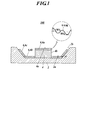
- the light emitting device 100 includes a package 2 having a concave cross section for mounting a light emitting element.
- a rectangular parallelepiped LED element 4 is arranged at the center of the recess of the package 2.
- Inside the package 2 there are a bottom surface 2a and an inner wall surface 2b.
- the bottom surface 2a is a flat surface, and the inner wall surface 2b is inclined upward from the inside toward the outside.
- the inclination angle (wall surface angle ⁇ ) of the inner wall surface 2b is set to 60 °, for example.
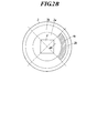
- the package 2 basically has a quadrangular outer shape, and the bottom surface 2a also has a quadrangular shape along the outer shape.
- the LED element 4 is an example of a light emitting element that emits light of a predetermined wavelength.
- the LED element 4 is flip-chip mounted on the package 2 via bumps (not shown).
- a blue LED element is used as the LED element 4.
- a blue LED element is formed by laminating an n-GaN-based cladding layer, an InGaN light-emitting layer, a p-GaN-based cladding layer, and a transparent electrode on a sapphire substrate.
- wavelength converting portions 6 (6a, 6b, 6c) are respectively formed on the upper surface 4a of the LED element 4, the bottom surface 2a of the package 2, and the inner wall surface 2b of the package 2, wavelength converting portions 6 (6a, 6b, 6c) are respectively formed.
- the wavelength conversion unit 6 is a part that converts light having a predetermined wavelength emitted from the LED element 4 into light having a different wavelength from the light having a wavelength different from the wavelength of the LED element 4 in the translucent ceramic layer.
- a phosphor that is excited to emit fluorescence having a wavelength different from the excitation wavelength is added.
- the thickness of each part of the wavelength conversion unit 6 is all within a range of ⁇ 30% with respect to the average thickness of the wavelength conversion unit 6 on the surface on which the wavelength conversion unit 6 is formed (see the enlarged portion in FIG. 1). That is, the thickness of each part of the wavelength conversion part 6a formed on the upper surface 4a of the LED element 4 is within a range of ⁇ 30% with respect to the average value of the thickness of the wavelength conversion part 6a.
- the thickness of each part of the wavelength conversion unit 6b formed on the bottom surface 2a of the package 2 is within a range of ⁇ 30% with respect to the average value of the thickness of the wavelength conversion unit 6b.
- the thickness of each part of the wavelength conversion unit 6c formed on the inner wall surface 2b of the package 2 is within a range of ⁇ 30% with respect to the average value of the thickness of the wavelength conversion unit 6c.
- the thickness of the wavelength converting portion 6c formed on the inner wall surface 2b of the package 2 is preferably 30 to 50% of the thickness of the wavelength converting portion 6a formed on the upper surface 4a of the LED element 4. That is, the wavelength conversion unit 6c is thinner than the wavelength conversion unit 6a, and specifically, the ratio of the thickness of the wavelength conversion unit 6c to the thickness of the wavelength conversion unit 6a is preferably 30 to 50%.
- the wavelength conversion unit 6 is not formed on the side surface 4 b of the LED element 4.
- the side surface 4b of the LED element 4 is basically exposed from between the wavelength conversion portions 6a and 6b formed on the bottom surface 2a of the package 2 and the top surface 4a of the LED element 4, and the inner wall surface 2b of the package 2 is exposed. It faces the wavelength converter 6c formed in the above.
- the side surface 4b of the LED element 4 does not necessarily have to be exposed, and a part (lower part) of the LED element 4 is covered with the wavelength conversion unit 6b.
- a portion (exposed portion) exposed from between the wavelength conversion units 6a and 6b is preferably exposed by 30 to 80% of the entire area of the side surface 4b.
- the area ratio of the wavelength conversion portion 6c formed on the inner wall surface 2b of the package 2 to the inner wall surface 2b is preferably 50% or more, and more preferably 60% or more. That is, as shown in FIG. 2A, the side surface 4b of the LED element 4 and the inner wall surface 2b of the package 2 exist in four surfaces, and each surface is opposed at 1: 1, but the inner wall surface 2b is seen on each surface. In this case, it is preferable that the area where the wavelength conversion portion 6c is formed occupies 50% or more by area ratio on all four surfaces. As shown in FIG. 2B, the package 2 may have a circular outer shape. In this case, the inner wall surface 2b of the package 2 is 90 ° in accordance with the number of side surfaces 4b of the LED element 4. It is only necessary to determine whether or not the formation region of the wavelength conversion unit 6c occupies 50% or more by area ratio for each region.
- the manufacturing method of the light emitting device 100 is mainly as follows. (1) Dispersing phosphor and at least one of swellable particles or inorganic particles in at least one of water or an organic solvent to prepare a first mixed solution; (2) The first mixed liquid is applied to the package 2 on which the LED element 4 is mounted and heated, and wavelength conversion is performed on the upper surface 4a of the LED element 4, the bottom surface 2a of the package 2, and the inner wall surface 2b of the package 2. Forming a precursor of the parts 6a, 6b, 6c; (3) a step of forming (completing) the wavelength conversion unit 6 by applying and heating the second mixed liquid in which the translucent ceramic precursor is dispersed in the solvent on the precursor of the wavelength conversion unit 6; , have.
- the phosphor and additives (swellable particles or inorganic particles) used in the step (1), the first mixed liquid, and the like will be described.
- the phosphor is excited by the wavelength (excitation wavelength) of light emitted from the LED element 4 and emits fluorescence having a wavelength different from the excitation wavelength.
- a YAG (yttrium, aluminum, garnet) phosphor that converts blue light (wavelength 420 nm to 485 nm) emitted from the blue LED element into yellow light (wavelength 550 nm to 650 nm) is used.
- Such phosphors use oxides of Y, Gd, Ce, Sm, Al, La, and Ga, or compounds that easily become oxides at high temperatures, and are mixed well in a stoichiometric ratio. A mixed raw material is obtained.
- a coprecipitated oxide obtained by calcining a solution obtained by coprecipitation of a solution obtained by dissolving a rare earth element of Y, Gd, Ce, or Sm in an acid with a stoichiometric ratio with oxalic acid, and aluminum oxide or gallium oxide.
- an appropriate amount of fluoride such as ammonium fluoride is mixed with the obtained mixed raw material as a flux and pressed to obtain a molded body.
- the obtained molded body is packed in a crucible and fired in air at a temperature range of 1350 to 1450 ° C. for 2 to 5 hours to obtain a sintered body having the light emission characteristics of a phosphor.
- the YAG phosphor is used.
- the type of the phosphor is not limited to this.
- other phosphors such as non-garnet phosphors containing no Ce are used. You can also.
- the larger the particle size of the phosphor the higher the light emission efficiency (wavelength conversion efficiency).
- the gap formed at the interface with the organometallic compound is increased, and the film strength of the formed ceramic layer is lowered. Accordingly, in consideration of the size of the gap generated at the interface between the light emission efficiency and the organometallic compound, it is preferable to use one having an average particle diameter of 1 ⁇ m or more and 50 ⁇ m or less.
- the average particle diameter of the phosphor can be measured, for example, by a Coulter counter method.
- the swellable particles include layered silicate minerals.
- the layered silicate mineral is preferably a swellable clay mineral having a structure such as a mica structure, a kaolinite structure, or a smectite structure, and particularly preferably a smectite structure rich in swellability. This is because by adding water to the mixed solution, a card house structure in which water enters and swells between layers of the smectite structure has an effect of greatly increasing the viscosity of the mixed solution. When the content of the layered silicate mineral in the ceramic layer is less than 1% by weight, the effect of increasing the viscosity of the mixed solution cannot be obtained sufficiently.
- the content of the layered silicate mineral exceeds 20% by weight, the strength of the ceramic layer after heating is lowered. Therefore, the content of the layered silicate mineral is preferably 1% by weight to 20% by weight, and more preferably 1% by weight to 10% by weight.
- a layered silicate mineral whose surface is modified (surface treatment) with an ammonium salt or the like can be used as appropriate.
- Inorganic particles have not only a thickening effect that increases the viscosity of the mixed solution, but also a filling effect that fills the gap generated at the interface between the organometallic compound and the phosphor, Also, it has a film strengthening effect for improving the film strength of the ceramic layer after heating.
- the inorganic particles used in the present invention include oxide fine particles such as silicon oxide, titanium oxide and zinc oxide, fluoride fine particles such as magnesium fluoride, and the like.
- silicon oxide fine particles such as silicon oxide, titanium oxide and zinc oxide
- fluoride fine particles such as magnesium fluoride, and the like.
- silicon oxide fine particles such as silicon oxide, titanium oxide and zinc oxide
- fluoride fine particles such as magnesium fluoride
- the content of the inorganic particles in the ceramic layer is preferably 1% by weight or more and 20% by weight or less, and more preferably 1% by weight or more and 10% by weight or less.
- the average particle diameter of the inorganic particles is preferably 0.001 ⁇ m or more and 50 ⁇ m or less in consideration of the above-described effects.
- the average particle diameter of the inorganic particles can be measured, for example, by a Coulter counter method.
- first mixed solution As a preparation procedure of the first mixed solution, swellable particles or inorganic particles are first premixed in an organic solvent, and then phosphor and / or water are mixed. . Alternatively, first, swellable particles or inorganic particles, a phosphor and water may be premixed, and then an organic solvent may be mixed. Thereby, swellable particle
- the viscosity of the first mixed solution is 10 to 500 cP, preferably 12 to 500 cP, more preferably 20 to 400 cP, and most preferably 100 to 300 cP. These viscosities were measured using a vibration viscometer (VM-10A-L manufactured by CBC).
- the first mixed liquid may contain only swellable particles, may contain only inorganic particles, or may contain both swellable particles and inorganic particles.
- step (2) the details of the step (2) will be described.
- the coating device 10 mainly includes a movable table 20 that can move up and down, right and left, and back and forth, and that can rotate, and a spray device 30 that can discharge the first mixed liquid (40) described above. ing.
- the spray device 30 is disposed above the movable table 20.
- the spray device 30 has a nozzle 32 into which air is sent, and an air compressor (not shown) for sending air is connected to the nozzle 32.
- the hole diameter at the tip of the nozzle 32 is 20 ⁇ m to 2 mm, preferably 0.1 to 0.3 mm.
- the nozzle 32 is movable up and down, left and right, and front and rear, like the moving table 20.
- Anest Iwata's spray gun W-101-142BPG is used as the nozzle 32
- Anest Iwata's OFP-071C is used as the compressor.
- the angle of the nozzle 32 can also be adjusted, and the nozzle 32 can be tilted with respect to the movable table 20 (or the package 2 installed thereon).
- the angle (spray angle ⁇ ) of the nozzle 32 with respect to the discharge target (package 2 or LED element 4) can be adjusted in the range of 0 to 90 ° when the horizontal direction is 0 °.
- a tank 36 is connected to the nozzle 32 via a connecting pipe 34.
- a first mixed solution 40 is stored in the tank 36.
- the tank 36 contains a stirring bar, and the first mixed liquid 40 is constantly stirred.
- the package 2 (with the LED element 4 mounted in advance) is placed on the moving table 20, and the package 2 and the spray are applied.
- the positional relationship with the nozzle 32 of the apparatus 30 is adjusted (position adjustment process).
- the package 2 is installed on the moving table 20, and the package 2 and the tip of the nozzle 32 are disposed to face each other.
- the first mixed liquid 40 can be uniformly applied as the distance between the package 2 and the nozzle 32 increases, but the film strength tends to decrease, so the distance between the package 2 and the tip of the nozzle 32. Is suitably kept in the range of 3 to 30 cm.
- the first mixed solution 40 is discharged from the nozzle 32, and the upper surface 4 a of the LED element 4, the bottom surface 2 a of the package 2, and the package
- the mixed liquid 40 is applied to the inner wall surface 2b of 2 (application process).
- the movable table 20 is rotated to rotate the package 2, and the movable table 20 and the nozzle 32 are moved to move the package 2 and the nozzle 32 back and forth and right and left. Either one of the moving table 20 and the nozzle 32 may be fixed, and the other may be moved back and forth and left and right.
- air is sent to the nozzle 32 and the first mixed solution 40 is discharged from the tip of the nozzle 32 toward the package 2.
- the distance between the package 2 and the nozzle 32 can be adjusted within the above range in consideration of the pressure of the air compressor.
- the pressure of the compressor is adjusted so that the pressure at the inlet (tip) of the nozzle 32 is 0.14 MPa.
- the first mixed liquid 40 can be applied to the upper surface of the LED element 4, the bottom surface 2a of the package 2, and the inner wall surface 2b of the package 2, and then the first mixed liquid 40 after application is applied.
- the precursors of the wavelength converters 6a, 6b, 6c can be formed.
- desired chromaticity can be obtained by adjusting the application amount of the first liquid mixture on the package by adjusting the spray distance, pressure, angle, and moving speed of the nozzle.
- the coating amount of the second mixed solution can be adjusted to obtain a desired film strength.
- the first mixed solution 40 When the first mixed solution 40 is applied to the inner wall surface 2b of the package 2, in the mixed solution in which the phosphor is simply mixed in the solvent, the phosphor is precipitated in the solvent, and the first mixed solution 40 It is difficult to apply such a uniform thickness. On the other hand, in this embodiment, since the swellable particles or the inorganic particles are contained in the first mixed liquid 40, the first mixed liquid 40 is thickened and the precipitation of the phosphor can be prevented. Application that makes the thickness of the first mixed solution 40 uniform can be performed. Furthermore, even when the first mixed solution 40 is applied to the upper surface 4a of the LED element 4, the first mixed solution 40 is thickened as described above, thereby preventing the phosphor from flowing down from the upper surface 4a. You can also
- the second liquid mixture is a solution in which a metal compound as a ceramic precursor is dispersed in a solvent, and is limited to the type of metal as long as a translucent ceramic can be formed. There is no.
- the second mixed solution may be a solution in which ceramics are formed by heating the gel after gelation by a reaction such as hydrolysis (sol-gel solution).
- the ceramic may be directly formed without gelation by volatilizing the solvent component.
- the metal compound may be an organic compound or an inorganic compound.
- preferable metal compounds include metal alkoxides, metal acetylacetonates, metal carboxylates, nitrates, and oxides. Of these, metal alkoxides are preferred because they are easily gelled by hydrolysis and polymerization reaction, and tetraethoxysilane is particularly preferred.
- a plurality of types of metal compounds may be used in combination.
- a 2nd liquid mixture it is preferable to contain suitably the water for hydrolysis, a solvent, a catalyst other than the said metal compound.
- the solvent include alcohols such as methanol, ethanol, propanol, and butanol.
- the catalyst include hydrochloric acid, sulfuric acid, nitric acid, acetic acid, hydrofluoric acid, ammonia and the like.
- tetraethoxysilane it is preferable to use 138 parts by mass of ethyl alcohol and 52 parts by mass of pure water with respect to 100 parts by mass of tetraethoxysilane.
- the heating temperature for heating the gel is preferably 120 to 500 ° C., and more preferably 120 to 150 ° C. from the viewpoint of further suppressing deterioration of the LED element 4 and the like.
- the heating temperature after coating is preferably 120 ° C. to 500 ° C., and more preferably 120 ° C. to 150 ° C. from the viewpoint of further suppressing deterioration of the LED element 4 and the like.
- Polysilazane can also be used as a ceramic precursor.
- the polysilazane used in the present invention is represented by the following general formula (i). (R 1 R 2 SiNR 3 ) n (i)
- R1, R2, and R3 each independently represent a hydrogen atom, an alkyl group, an aryl group, a vinyl group, or a cycloalkyl group, and at least one of R1, R2, and R3 is a hydrogen atom.
- n represents an integer of 1 to 60.
- the molecular shape of polysilazane may be any shape, for example, linear or cyclic.
- Polysilazane represented by the above formula (i) and a reaction accelerator as required are dissolved in an appropriate solvent and cured by heating, excimer light treatment, UV light treatment, and excellent heat resistance and light resistance.
- a ceramic film can be made.
- the effect of preventing penetration of moisture can be further improved by heat curing after irradiation with UVU radiation (eg, excimer light) containing a wavelength component in the range of 170 to 230 nm.
- UVU radiation eg, excimer light
- an acid, a base, or the like is preferably used, but it may not be used.
- reaction accelerators include triethylamine, diethylamine, N, N-diethylethanolamine, N, N-dimethylethanolamine, triethanolamine, triethylamine, hydrochloric acid, oxalic acid, fumaric acid, sulfonic acid, acetic acid, nickel, iron, palladium , Metal carboxylates including iridium, platinum, titanium, and aluminum, but are not limited thereto. Particularly preferred when a reaction accelerator is used is a metal carboxylate, and the addition amount is preferably 0.01 to 5 mol% based on polysilazane.
- the solvent aliphatic hydrocarbons, aromatic hydrocarbons, halogen hydrocarbons, ethers, and esters can be used.
- methyl ethyl ketone Preferred are methyl ethyl ketone, tetrahydrofuran, benzene, toluene, xylene, dimethyl fluoride, chloroform, carbon tetrachloride, ethyl ether, isopropyl ether, dibutyl ether, and ethyl butyl ether.
- the polysilazane concentration is preferably higher, but since the increase in concentration leads to a shortening of the polysilazane storage period, the polysilazane is preferably dissolved in the solvent at 5% by mass or more and 50% by mass or less.
- the wavelength conversion portion 6c is formed on the inner wall surface 2b of the package 2 in addition to the upper surface 4a of the LED element 4 and the bottom surface 2a of the package 2, the side surface 4b of the LED element 4 is formed.
- the light emitted from the light enters the wavelength converter 6c of the inner wall surface 2b of the package 2 and is wavelength-converted.
- the thickness of each wavelength conversion part 6a, 6b, 6c formed in the upper surface 4a of the LED element 4, the bottom face 2a of the package 2, and the inner wall surface 2b of the package 2 is settled in a predetermined range, and a wavelength conversion part is each surface. Since the thickness of 6a, 6b, 6c is made uniform, the occurrence of color misregistration can be suppressed as a result.
- Sample preparation (1.1) Package and blue LED A blue LED having a size of 200 ⁇ m in length, 200 ⁇ m in width, and 200 ⁇ m in height was mounted in a flip chip type in a circular package having an opening diameter of 3 mm, a bottom surface diameter of 2 mm, and a wall surface angle of 60 °.
- (1.2) Fluorescent substance Yellow fluorescent particles prepared by the following method were used. A mixture in which the following phosphor raw materials are sufficiently mixed is filled in an aluminum crucible, and an appropriate amount of fluoride such as ammonium fluoride is mixed therein as a flux, and 1350 to 1450 ° C. in a reducing atmosphere in which hydrogen-containing nitrogen gas is circulated. And calcined for 2 to 5 hours in the temperature range, to obtain a calcined product ((Y 0.72 Gd 0.24 ) 3 Al 5 O 12 : Ce 0.04 ).
- fluoride such as ammonium fluoride
- the fired product obtained was pulverized, washed, separated, and dried to obtain a desired phosphor.
- the obtained phosphor was pulverized into phosphor particles having a particle size of about 10 ⁇ m.
- the composition of the obtained phosphor was examined, it was confirmed that the phosphor was a desired phosphor.
- the emission wavelength of excitation light having a wavelength of 465 nm was examined, it had a peak wavelength at a wavelength of approximately 570 nm.
- the coating device used was the coating device shown in FIG.
- a spray gun W-101-142BPG manufactured by Anest Iwata Co., Ltd. was used as a spray device nozzle (spray nozzle).
- the distance from the spray nozzle to the sample was 15 cm.
- the spray pressure was 0.1 MPa.
- the “spray angle” is an angle ( ⁇ in FIG. 3) in which the spray nozzle is inclined toward the upper side of the package when the horizontal direction is 0 °.
- “Distance” is the distance from the tip of the spray nozzle to the sample when the spray nozzle passes just above the package.
- polysilazane (NN120-20 wt% manufactured by AZ Electronic Materials Co., Ltd.) is spray-applied in the vertical direction (at a spray angle of 90 °) from the wavelength conversion unit precursor with the coating apparatus of FIG.
- the sample of “Comparative Example 1” was produced by fixing the wavelength conversion part by time baking to complete.
- the spray coating in this case was performed by passing the spray nozzle through the package at a speed of 70 mm / s while discharging polysilazane at a pressure of 0.1 MPa.
- the distance from the spray nozzle to the sample was 15 cm
- Example 1 In the step of spray-coating a mixed solution containing phosphors and the like, the spray angle was 40 °, and the distance from the spray nozzle to the sample was 10 cm. In the step of spray-coating polysilazane, the distance from the spray nozzle to the sample was 10 cm. A sample of “Example 1” was produced in the same manner as Comparative Example 1 except for these.
- Example 2 In the step of spray-coating a mixed solution containing phosphors and the like, the spray angle was 50 °, and the distance from the spray nozzle to the sample was 10 cm. In the step of spray-coating polysilazane, the distance from the spray nozzle to the sample was 10 cm. A sample of “Example 2” was produced in the same manner as in Comparative Example 1 except for these.
- Example 3 In the step of spray-coating a mixed solution containing phosphors and the like, the spray angle was 65 °, and the distance from the spray nozzle to the sample was 10 cm. In the step of spray-coating polysilazane, the distance from the spray nozzle to the sample was 10 cm. A sample of “Example 3” was produced in the same manner as in Comparative Example 1 except for these.
- Example 4 In the step of spray-coating a mixed solution containing phosphors and the like, the spray angle was 60 °, and the distance from the spray nozzle to the sample was 12 cm. In the step of spraying polysilazane, the distance from the spray nozzle to the sample was 12 cm. A sample of “Example 4” was produced in the same manner as in Comparative Example 1 except for these.
- Example 5 In the step of spray-coating a mixed solution containing phosphors and the like, the spray angle was 60 °, and the distance from the spray nozzle to the sample was 15 cm. In the step of spraying polysilazane, the distance from the spray nozzle to the sample was 15 cm. A sample of “Example 5” was produced in the same manner as in Comparative Example 1 except for these.
- Example 6 Inorganic particles (RX300 manufactured by Nippon Aerosil Co., Ltd., 0.1 parts by weight) and 0.75 parts by weight of the prepared phosphor were mixed in 0.5 parts by weight of water, and further 1 part of isopropyl alcohol (IPA). Parts were mixed to prepare a mixed solution. Then, using the coating apparatus of FIG. 3, while rotating the package, the spray nozzle was passed over the package at a speed of 150 mm / s to spray the mixed solution. At this time, the spray angle was 65 °, the distance from the spray nozzle to the sample was 10 cm, and the spray pressure was 0.1 MPa.
- IPA isopropyl alcohol
- the spray angle was set to 40 °, and the spray nozzle was passed over the package at a speed of 150 mm / s to spray the mixture.
- the distance from the spray nozzle to the sample was 10 cm, and the spray pressure was 0.1 MPa.
- the coated mixture was dried at 50 ° C. for 1 hour to prepare a wavelength conversion portion precursor.
- polysilazane (NN120-20 wt% manufactured by AZ Electronic Materials Co., Ltd.) is spray-applied in the vertical direction (at a spray angle of 90 °) from the wavelength conversion portion precursor using the coating apparatus shown in FIG.
- the sample was fired for 1 hour to fix and complete the wavelength conversion part, and a sample of “Example 6” was produced.
- the spray coating in this case was performed by passing the spray nozzle through the package at a speed of 70 mm / s while discharging polysilazane at a pressure of 0.1 MPa.
- the distance from the spray nozzle to the sample was 15 cm.
- Example 7 Inorganic particles (RX300 manufactured by Nippon Aerosil Co., Ltd., 0.1 parts by weight) and 0.75 parts by weight of the prepared phosphor were mixed in 0.5 parts by weight of water, and further 1 part of isopropyl alcohol (IPA). Parts were mixed to prepare a mixed solution. Then, using the coating apparatus of FIG. 3, while rotating the package, the spray nozzle was passed over the package at a speed of 150 mm / s to spray the mixed solution. At this time, the spray angle was 65 °, the distance from the spray nozzle to the sample was 10 cm, and the spray pressure was 0.1 MPa.
- IPA isopropyl alcohol
- the spray nozzle was passed through the package at a spray angle of 150 mm / s at a spray angle of 50 °, and the mixture was spray-coated. At this time, the distance from the spray nozzle to the sample was 10 cm, and the spray pressure was 0.1 MPa. After the two spray coatings, the coated mixture was dried at 50 ° C. for 1 hour to prepare a wavelength conversion portion precursor. Thereafter, polysilazane (NN120-20 wt% manufactured by AZ Electronic Materials Co., Ltd.) is spray-applied in the vertical direction (at a spray angle of 90 °) from the wavelength conversion portion precursor using the coating apparatus shown in FIG.
- Example 7 a sample of “Example 7” was produced.
- the spray coating in this case was performed by passing the spray nozzle through the package at a speed of 70 mm / s while discharging polysilazane at a pressure of 0.1 MPa. The distance from the spray nozzle to the sample was 15 cm.
- Example 8 Swellable particles (hydrophilic smectite (Lucentite SWN, manufactured by Co-op Chemical Co., Ltd.) (0.1 part by weight) and the prepared phosphor (0.75 part by weight) were mixed in water (0.5 part by weight), and isopropyl alcohol (IPA ) 1 part by weight was mixed to prepare a mixed solution. Thereafter, using the coating apparatus shown in FIG. 3, the spray solution was applied by spraying the spray nozzle through the package at a speed of 150 mm / s while rotating the package. At this time, the spray angle was 65 °, the distance from the spray nozzle to the sample was 10 cm, and the spray pressure was 0.1 MPa.
- the spray angle was set to 40 ° and the spray nozzle was passed over the package at a speed of 150 mm / s to spray the mixture. At this time, the distance from the spray nozzle to the sample was 8 cm, and the spray pressure was 0.1 MPa.
- the coated mixture was dried at 50 ° C. for 1 hour to prepare a wavelength conversion portion precursor.
- polysilazane (NN120-20 wt% manufactured by AZ Electronic Materials Co., Ltd.) is spray-applied in the vertical direction (at a spray angle of 90 °) from the wavelength conversion portion precursor using the coating apparatus shown in FIG.
- Example 8 a sample of “Example 8” was produced.
- the spray coating in this case was performed by passing the spray nozzle through the package at a speed of 70 mm / s while discharging polysilazane at a pressure of 0.1 MPa. The distance from the spray nozzle to the sample was 15 cm.
- Example 9 Swellable particles (0.02 parts by weight of hydrophilic smectite (Lucentite SWN, manufactured by Corp Chemical) and 0.83 parts by weight of the prepared phosphor were mixed in 0.5 parts by weight of water, and further isopropyl alcohol (IPA ) 1 part by weight was mixed to prepare a mixed solution. Thereafter, using the coating apparatus shown in FIG. 3, the spray solution was applied by spraying the spray nozzle through the package at a speed of 150 mm / s while rotating the package. At this time, the spray angle was 65 °, the distance from the spray nozzle to the sample was 10 cm, and the spray pressure was 0.1 MPa.
- IPA isopropyl alcohol
- the spray angle was set to 40 ° and the spray nozzle was passed over the package at a speed of 150 mm / s to spray the mixture. At this time, the distance from the spray nozzle to the sample was 8 cm, and the spray pressure was 0.1 MPa.
- the coated mixture was dried at 50 ° C. for 1 hour to prepare a wavelength conversion portion precursor. Thereafter, using the coating apparatus shown in FIG. 3, a polysiloxane dispersion (polysiloxane 14% by mass, IPA 86% by mass) is spray-applied in a vertical direction (at a spray angle of 90 °) from the precursor of the wavelength conversion unit, and 150 A sample of “Example 9” was produced by baking at 1 ° C.
- the spray coating in this case was performed by passing the spray nozzle through the package at a speed of 90 mm / s while discharging polysiloxane at a pressure of 0.1 MPa. The distance from the spray nozzle to the sample was 15 cm.
- Example 10 Phosphor 0.75 prepared with swellable particles (0.05 parts by weight of hydrophilic smectite (Lucentite SWN, manufactured by Corp Chemical) and 0.05 parts by weight of inorganic particles (RX300 manufactured by Nippon Aerosil Co., Ltd., particle size: 7 nm) Part by weight was mixed with 0.5 part by weight of water, and 1 part by weight of isopropyl alcohol (IPA) was further mixed to prepare a mixed solution. Thereafter, using the coating apparatus shown in FIG. 3, the spray solution was applied by spraying the spray nozzle through the package at a speed of 150 mm / s while rotating the package.
- IPA isopropyl alcohol
- the spray angle was 65 °
- the distance from the spray nozzle to the sample was 8 cm
- the spray pressure was 0.1 MPa.
- the spray angle was set to 40 ° and the spray nozzle was passed over the package at a speed of 150 mm / s to spray the mixture.
- the distance from the spray nozzle to the sample was 6 cm
- the spray pressure was 0.1 MPa.
- the coated mixture was dried at 50 ° C. for 1 hour to prepare a wavelength conversion portion precursor. Thereafter, using the coating apparatus shown in FIG.
- a polysiloxane dispersion (polysiloxane 14% by mass, IPA 86% by mass) is spray-applied in a vertical direction (at a spray angle of 90 °) from the precursor of the wavelength conversion unit, and 150
- a sample of “Example 10” was produced by baking at 1 ° C. for 1 hour to fix and complete the wavelength conversion part.
- the spray coating in this case was performed by passing the spray nozzle through the package at a speed of 90 mm / s while discharging polysiloxane at a pressure of 0.1 MPa. The distance from the spray nozzle to the sample was 15 cm.
- ⁇ greater than 0.05 “ ⁇ ”: greater than 0.03 and less than or equal to 0.05 “ ⁇ ”: greater than 0.01 and less than or equal to 0.0 “ ⁇ ”: greater than 0.005 , 0.01 or less “ ⁇ ” ... 0.005 or less
- the thickness of the wavelength conversion portion on the inner wall surface of the package to 30 to 50% of the thickness of the wavelength conversion portion on the upper surface of the LED element. Furthermore, it is useful to control the area ratio of the exposed portion on the side surface of the LED element to 30 to 80%, or to control the area ratio of the wavelength conversion portion to the area of the inner wall surface of the package to 50% or more. .
- the present invention can be suitably used to suppress the occurrence of color misregistration.
Landscapes
- Led Device Packages (AREA)
Abstract
発光装置(100)は、内壁面(2b)が傾斜した凹状のパッケージ(2)と、パッケージ(2)の底面(2a)に配置されたLED素子(4)と、LED素子(4)の出射光を特定波長の光に変換する波長変換部(6)と、を備える。発光装置(100)では、波長変換部(6)がLED素子(4)の上面(4a)、パッケージ(2)の底面(2a)およびパッケージ(2)の内壁面(2b)に形成され、これら各面の波長変換部(6)の厚みがすべて、その面の波長変換部(6)の厚みの平均値に対して±30%の範囲内に収まっている。
Description
本発明は発光装置およびその製造方法に関する。
従来から、照明などの用途において、LED素子などの発光素子の光を励起光として用いて蛍光体を発光させ、白色光を得る発光装置が開発されている。
このような発光装置としては、たとえば、発光素子から出射された青色光により黄色光を出射する蛍光体を用い、それぞれの光を混色させることで白色光とする発光装置や、発光素子から出射された紫外光により青色・緑色・赤色の光を出射する蛍光体を用いて、蛍光体から出射された3色の光を混色させることで白色光とする発光装置などが知られている。
このような発光装置としては、たとえば、発光素子から出射された青色光により黄色光を出射する蛍光体を用い、それぞれの光を混色させることで白色光とする発光装置や、発光素子から出射された紫外光により青色・緑色・赤色の光を出射する蛍光体を用いて、蛍光体から出射された3色の光を混色させることで白色光とする発光装置などが知られている。
このような発光装置の構成として、発光素子を、蛍光体が分散された封止材により直接的に封止した発光装置が開発されている。当該発光装置では、蛍光体が分散された上記封止材が「波長変換部」に相当する。
ただ、このような発光装置の特性として、発光素子の光と蛍光体による蛍光とを混色して白色光を得ようとする関係上、発光装置を正面から見た場合に色ズレが発生することがある。ここでいう「色ズレ」とは、発光装置を正面から見た場合に、通常、青色・黄色の混色(または青色・緑色・赤色の混色)による白色領域が形成されるが、適切に混色されずに、黄色光や青色光(または青色光や緑色光、赤色光)による領域が部分的に形成される現象をいう。
ただ、このような発光装置の特性として、発光素子の光と蛍光体による蛍光とを混色して白色光を得ようとする関係上、発光装置を正面から見た場合に色ズレが発生することがある。ここでいう「色ズレ」とは、発光装置を正面から見た場合に、通常、青色・黄色の混色(または青色・緑色・赤色の混色)による白色領域が形成されるが、適切に混色されずに、黄色光や青色光(または青色光や緑色光、赤色光)による領域が部分的に形成される現象をいう。
このような色ズレの問題に対する技術が特許文献1,2に開示されている。
特許文献1の技術では、発光素子(LEDチップ103)の上面と、発光素子を実装するためのパッケージ(102)の底面とに対して波長変換部(コーティング材111,112)を形成し、これら波長変換部の厚みを略等しく均一とすることにより、色ズレを抑制しようとしている(段落0018や図1など参照)。
特許文献2の技術では、発光素子(13)を実装するためのパッケージ(12)の凹部を、特殊なシリコーン樹脂(樹脂層15および封止樹脂14)で充填し、発光素子全体を樹脂製の波長変換部で被覆することにより、波長変換部のパッケージからの剥離を防止しつつ、色ズレを抑制しようとしている(段落0050~0054や図5~図9など参照)。
特許文献1の技術では、発光素子(LEDチップ103)の上面と、発光素子を実装するためのパッケージ(102)の底面とに対して波長変換部(コーティング材111,112)を形成し、これら波長変換部の厚みを略等しく均一とすることにより、色ズレを抑制しようとしている(段落0018や図1など参照)。
特許文献2の技術では、発光素子(13)を実装するためのパッケージ(12)の凹部を、特殊なシリコーン樹脂(樹脂層15および封止樹脂14)で充填し、発光素子全体を樹脂製の波長変換部で被覆することにより、波長変換部のパッケージからの剥離を防止しつつ、色ズレを抑制しようとしている(段落0050~0054や図5~図9など参照)。
しかしながら、特許文献1,2の技術によっても下記のような課題が残る。
特許文献1の技術によれば、発光素子の上面とパッケージの底面とに対し均一な厚みの波長変換部を作製しても、発光素子の側面から光が出射され、その出射光が一部波長変換されずに発光装置の外へ放出されるため、色ズレが発生してしまう。
特許文献2の技術によれば、パッケージの凹部中で発光素子全体を覆うように波長変換部を作製した場合でも、発光素子の角部などにおいて波長変換部の厚みが不均一となり、色ズレが発生してしまう。
特許文献1の技術によれば、発光素子の上面とパッケージの底面とに対し均一な厚みの波長変換部を作製しても、発光素子の側面から光が出射され、その出射光が一部波長変換されずに発光装置の外へ放出されるため、色ズレが発生してしまう。
特許文献2の技術によれば、パッケージの凹部中で発光素子全体を覆うように波長変換部を作製した場合でも、発光素子の角部などにおいて波長変換部の厚みが不均一となり、色ズレが発生してしまう。
したがって、本発明の主な目的は、色ズレの発生を抑制することができる発光装置およびその製造方法を提供することにある。
上記課題を解決するため本発明の一態様によれば、
内壁面が傾斜した凹状のパッケージと、
前記パッケージの底面に配置されたLED素子と、
前記LED素子の出射光を特定波長の光に変換する波長変換部と、
を備える発光装置において、
前記波長変換部が前記LED素子の上面、前記パッケージの底面および前記パッケージの内壁面に形成され、これら各面の前記波長変換部の厚みがすべて、その面の前記波長変換部の厚みの平均値に対して±30%の範囲内に収まっていることを特徴とする発光装置が提供される。
内壁面が傾斜した凹状のパッケージと、
前記パッケージの底面に配置されたLED素子と、
前記LED素子の出射光を特定波長の光に変換する波長変換部と、
を備える発光装置において、
前記波長変換部が前記LED素子の上面、前記パッケージの底面および前記パッケージの内壁面に形成され、これら各面の前記波長変換部の厚みがすべて、その面の前記波長変換部の厚みの平均値に対して±30%の範囲内に収まっていることを特徴とする発光装置が提供される。
本発明の他の態様によれば、
内壁面が傾斜した凹状のパッケージと、
前記パッケージの底面に配置された発光素子と、
前記発光素子の出射光を特定波長の光に変換する波長変換部と、
を備える発光装置の製造方法において、
蛍光体と、膨潤性粒子または無機粒子の少なくとも一方とを、水または有機溶媒の少なくとも一方に分散し、第1の混合液を調製する工程と、
前記第1の混合液を、前記発光素子を実装した前記パッケージ上に塗布して加熱し、前記発光素子の上面、前記パッケージの底面および前記パッケージの内壁面に対し、前記波長変換部の前駆体を形成する工程と、
透光性のセラミック前駆体を溶媒に分散した第2の混合液を、前記波長変換部の前駆体上に塗布して加熱し、前記波長変換部を形成する工程と、
を有することを特徴とする発光装置の製造方法が提供される。
内壁面が傾斜した凹状のパッケージと、
前記パッケージの底面に配置された発光素子と、
前記発光素子の出射光を特定波長の光に変換する波長変換部と、
を備える発光装置の製造方法において、
蛍光体と、膨潤性粒子または無機粒子の少なくとも一方とを、水または有機溶媒の少なくとも一方に分散し、第1の混合液を調製する工程と、
前記第1の混合液を、前記発光素子を実装した前記パッケージ上に塗布して加熱し、前記発光素子の上面、前記パッケージの底面および前記パッケージの内壁面に対し、前記波長変換部の前駆体を形成する工程と、
透光性のセラミック前駆体を溶媒に分散した第2の混合液を、前記波長変換部の前駆体上に塗布して加熱し、前記波長変換部を形成する工程と、
を有することを特徴とする発光装置の製造方法が提供される。
本発明によれば、発光素子の上面およびパッケージの底面に加えて、パッケージの内壁面にも波長変換部が形成されているから、発光素子の側面から出射された光はパッケージの内壁面の波長変換部に入射し波長変換されるし、発光素子の上面、パッケージの底面およびパッケージの内壁面に形成された波長変換部の厚みが所定の範囲内に収まっているから、各面で波長変換部の厚みが均一化され、その結果、色ズレの発生を抑制することができる。
以下、図面を参照しながら本発明の好ましい実施形態について説明する。
図1に示すとおり、発光装置100は、発光素子を実装するための断面凹状のパッケージ2を有している。パッケージ2の凹部の中央部には直方体状のLED素子4が配置されている。
パッケージ2の内部には底面2aと内壁面2bとが存在している。底面2aは平坦面となっており、内壁面2bは内側から外側に向けて上方に傾斜している。内壁面2bの傾斜角度(壁面角度α)はたとえば60°とされている。
図2Aに示すとおり、基本的には、パッケージ2は外形が四角形状を呈しており、底面2aもその外形に沿う四角形状を呈している。
パッケージ2の内部には底面2aと内壁面2bとが存在している。底面2aは平坦面となっており、内壁面2bは内側から外側に向けて上方に傾斜している。内壁面2bの傾斜角度(壁面角度α)はたとえば60°とされている。
図2Aに示すとおり、基本的には、パッケージ2は外形が四角形状を呈しており、底面2aもその外形に沿う四角形状を呈している。
LED素子4は所定波長の光を出射する発光素子の一例である。LED素子4はバンプ(図示略)を介してパッケージ2にフリップチップ実装されている。
本実施形態では、LED素子4として青色LED素子を用いている。青色LED素子は、例えばサファイア基板上にn-GaN系クラッド層、InGaN発光層、p-GaN系クラッド層、及び透明電極を積層してなる。
本実施形態では、LED素子4として青色LED素子を用いている。青色LED素子は、例えばサファイア基板上にn-GaN系クラッド層、InGaN発光層、p-GaN系クラッド層、及び透明電極を積層してなる。
LED素子4の上面4a、パッケージ2の底面2aおよびパッケージ2の内壁面2bには、波長変換部6(6a,6b,6c)がそれぞれ形成されている。
波長変換部6は、LED素子4から出射される所定波長の光を、これとは異なる長波長の光に変換する部分であり、透光性を有するセラミック層中にLED素子4からの波長により励起されて、励起波長と異なる波長の蛍光を出す蛍光体が添加されている。
波長変換部6は、LED素子4から出射される所定波長の光を、これとは異なる長波長の光に変換する部分であり、透光性を有するセラミック層中にLED素子4からの波長により励起されて、励起波長と異なる波長の蛍光を出す蛍光体が添加されている。
波長変換部6の各部の厚みはすべて、それが形成された面の波長変換部6の厚みの平均値に対して±30%の範囲内に収まっている(図1中拡大部参照)。
すなわち、LED素子4の上面4aに形成された波長変換部6aの各部の厚みは、波長変換部6aの厚みの平均値に対して±30%の範囲内に収まっている。パッケージ2の底面2aに形成された波長変換部6bの各部の厚みは、波長変換部6bの厚みの平均値に対して±30%の範囲内に収まっている。パッケージ2の内壁面2bに形成された波長変換部6cの各部の厚みは、波長変換部6cの厚みの平均値に対して±30%の範囲内に収まっている。
すなわち、LED素子4の上面4aに形成された波長変換部6aの各部の厚みは、波長変換部6aの厚みの平均値に対して±30%の範囲内に収まっている。パッケージ2の底面2aに形成された波長変換部6bの各部の厚みは、波長変換部6bの厚みの平均値に対して±30%の範囲内に収まっている。パッケージ2の内壁面2bに形成された波長変換部6cの各部の厚みは、波長変換部6cの厚みの平均値に対して±30%の範囲内に収まっている。
パッケージ2の内壁面2bに形成された波長変換部6cの厚みは、好ましくはLED素子4の上面4aに形成された波長変換部6aの厚みの30~50%である。
すなわち、波長変換部6cは波長変換部6aより厚みが小さく、具体的には波長変換部6aの厚みに対する波長変換部6cの厚みの割合が30~50%であるのがよい。
すなわち、波長変換部6cは波長変換部6aより厚みが小さく、具体的には波長変換部6aの厚みに対する波長変換部6cの厚みの割合が30~50%であるのがよい。
図1に示すとおり、LED素子4の側面4bには波長変換部6が形成されていない。LED素子4の側面4bは、基本的には、パッケージ2の底面2aとLED素子4の上面4aとに形成された波長変換部6a,6bの間から露出しており、パッケージ2の内壁面2bに形成された波長変換部6cと対向している。
LED素子4の側面4bはすべて露出している必要はなく、その一部(下部)が波長変換部6bで被覆されている。LED素子4の側面4bのうち、波長変換部6a,6bの間から露出した部分(露出部)が、側面4bのすべての面積の30~80%露出しているのがよい。
LED素子4の側面4bはすべて露出している必要はなく、その一部(下部)が波長変換部6bで被覆されている。LED素子4の側面4bのうち、波長変換部6a,6bの間から露出した部分(露出部)が、側面4bのすべての面積の30~80%露出しているのがよい。
パッケージ2の内壁面2bに形成された波長変換部6cの内壁面2bに占める面積比は、好ましくは50%以上であり、さらに好ましくは60%以上である。
すなわち、図2Aに示すとおり、LED素子4の側面4bとパッケージ2の内壁面2bはそれぞれ4面ずつ存在し各面が1:1で対向しているが、内壁面2bを1面ごとに見た場合に、4面すべてにおいて、波長変換部6cの形成領域が面積比で50%以上占めているのがよい。
なお、図2Bに示すとおり、パッケージ2は外形が円形状を呈するものであってもよく、この場合には、LED素子4の側面4bの面数に合わせてパッケージ2の内壁面2bを90°ずつ4分割し、各領域ごとに、波長変換部6cの形成領域が面積比で50%以上占めているかどうかを判断すればよい。
すなわち、図2Aに示すとおり、LED素子4の側面4bとパッケージ2の内壁面2bはそれぞれ4面ずつ存在し各面が1:1で対向しているが、内壁面2bを1面ごとに見た場合に、4面すべてにおいて、波長変換部6cの形成領域が面積比で50%以上占めているのがよい。
なお、図2Bに示すとおり、パッケージ2は外形が円形状を呈するものであってもよく、この場合には、LED素子4の側面4bの面数に合わせてパッケージ2の内壁面2bを90°ずつ4分割し、各領域ごとに、波長変換部6cの形成領域が面積比で50%以上占めているかどうかを判断すればよい。
続いて、発光装置100の製造方法について説明する。
発光装置100の製造方法は、主には、
(1)蛍光体と、膨潤性粒子または無機粒子の少なくとも一方とを、水または有機溶媒の少なくとも一方に分散し、第1の混合液を調製する工程と、
(2)第1の混合液を、LED素子4を実装したパッケージ2上に塗布して加熱し、LED素子4の上面4a、パッケージ2の底面2aおよびパッケージ2の内壁面2bに対し、波長変換部6a,6b,6cの前駆体を形成する工程と、
(3)透光性のセラミック前駆体を溶媒に分散した第2の混合液を、波長変換部6の前駆体上に塗布して加熱し、波長変換部6を形成する(完成させる)工程と、
を有している。
(1)蛍光体と、膨潤性粒子または無機粒子の少なくとも一方とを、水または有機溶媒の少なくとも一方に分散し、第1の混合液を調製する工程と、
(2)第1の混合液を、LED素子4を実装したパッケージ2上に塗布して加熱し、LED素子4の上面4a、パッケージ2の底面2aおよびパッケージ2の内壁面2bに対し、波長変換部6a,6b,6cの前駆体を形成する工程と、
(3)透光性のセラミック前駆体を溶媒に分散した第2の混合液を、波長変換部6の前駆体上に塗布して加熱し、波長変換部6を形成する(完成させる)工程と、
を有している。
はじめに、(1)の工程で使用する蛍光体や添加剤(膨潤性粒子または無機粒子)、第1の混合液などについて説明する。
(1.1)蛍光体
蛍光体は、LED素子4からの出射光の波長(励起波長)により励起されて、励起波長と異なる波長の蛍光を出射するものである。本実施形態では、青色LED素子から出射される青色光(波長420nm~485nm)を黄色光(波長550nm~650nm)に変換するYAG(イットリウム・アルミニウム・ガーネット)蛍光体を使用している。
このような蛍光体は、Y、Gd、Ce、Sm、Al、La、Gaの酸化物、または高温で容易に酸化物となる化合物を使用し、それらを化学量論比で十分に混合して混合原料を得る。或いは、Y、Gd、Ce、Smの希土類元素を化学量論比で酸に溶解した溶液をシュウ酸で共沈したものを焼成して得られる共沈酸化物と、酸化アルミニウム、酸化ガリウムとを混合して混合原料を得る。そして、得られた混合原料にフラックスとしてフッ化アンモニウム等のフッ化物を適量混合して加圧し、成形体を得る。得られた成形体を坩堝に詰め、空気中1350~1450℃の温度範囲で2~5時間焼成し、蛍光体の発光特性を持つ焼結体を得る。
なお、本実施形態ではYAG蛍光体を使用しているが、蛍光体の種類はこれに限定されるものではなく、例えばCeを含まない非ガーネット系蛍光体等の他の蛍光体を使用することもできる。また、蛍光体の粒径が大きいほど発光効率(波長変換効率)は高くなる反面、有機金属化合物との界面に生じる隙間が大きくなって形成されたセラミック層の膜強度が低下する。従って、発光効率と有機金属化合物との界面に生じる隙間の大きさを考慮し、平均粒径が1μm以上50μm以下のものを用いることが好ましい。蛍光体の平均粒径は、例えばコールターカウンター法によって測定することができる。
蛍光体は、LED素子4からの出射光の波長(励起波長)により励起されて、励起波長と異なる波長の蛍光を出射するものである。本実施形態では、青色LED素子から出射される青色光(波長420nm~485nm)を黄色光(波長550nm~650nm)に変換するYAG(イットリウム・アルミニウム・ガーネット)蛍光体を使用している。
このような蛍光体は、Y、Gd、Ce、Sm、Al、La、Gaの酸化物、または高温で容易に酸化物となる化合物を使用し、それらを化学量論比で十分に混合して混合原料を得る。或いは、Y、Gd、Ce、Smの希土類元素を化学量論比で酸に溶解した溶液をシュウ酸で共沈したものを焼成して得られる共沈酸化物と、酸化アルミニウム、酸化ガリウムとを混合して混合原料を得る。そして、得られた混合原料にフラックスとしてフッ化アンモニウム等のフッ化物を適量混合して加圧し、成形体を得る。得られた成形体を坩堝に詰め、空気中1350~1450℃の温度範囲で2~5時間焼成し、蛍光体の発光特性を持つ焼結体を得る。
なお、本実施形態ではYAG蛍光体を使用しているが、蛍光体の種類はこれに限定されるものではなく、例えばCeを含まない非ガーネット系蛍光体等の他の蛍光体を使用することもできる。また、蛍光体の粒径が大きいほど発光効率(波長変換効率)は高くなる反面、有機金属化合物との界面に生じる隙間が大きくなって形成されたセラミック層の膜強度が低下する。従って、発光効率と有機金属化合物との界面に生じる隙間の大きさを考慮し、平均粒径が1μm以上50μm以下のものを用いることが好ましい。蛍光体の平均粒径は、例えばコールターカウンター法によって測定することができる。
(1.2)添加剤
第1の混合液の粘度を調整する方法としては膨潤性粒子や無機粒子を溶媒に添加する手法が挙げられるが、第1の混合液を増粘することができればいかなる手法を用いることが可能であり、これに限定されるわけではない。
第1の混合液の粘度を調整する方法としては膨潤性粒子や無機粒子を溶媒に添加する手法が挙げられるが、第1の混合液を増粘することができればいかなる手法を用いることが可能であり、これに限定されるわけではない。
(1.2.1)膨潤性粒子
膨潤性粒子としては例えば層状ケイ酸塩鉱物が挙げられる。
層状ケイ酸塩鉱物は、雲母構造、カオリナイト構造、スメクタイト構造等の構造を有する膨潤性粘土鉱物が好ましく、膨潤性に富むスメクタイト構造が特に好ましい。これは混合液中に水を添加することで、スメクタイト構造の層間に水が進入して膨潤したカードハウス構造をとるため、混合液の粘性を大幅に増加させる効果があるためである。
セラミック層中における層状ケイ酸塩鉱物の含有量が1重量%未満になると混合液の粘性を増加させる効果が十分に得られない。一方、層状ケイ酸塩鉱物の含有量が20重量%を超えると加熱後のセラミック層の強度が低下する。従って、層状ケイ酸塩鉱物の含有量は1重量%以上20重量%以下とすることが好ましく、1重量%以上10重量%以下がより好ましい。
なお、有機溶媒との相溶性を考慮して、層状ケイ酸塩鉱物の表面をアンモニウム塩等で修飾(表面処理)したものを適宜用いることもできる。
膨潤性粒子としては例えば層状ケイ酸塩鉱物が挙げられる。
層状ケイ酸塩鉱物は、雲母構造、カオリナイト構造、スメクタイト構造等の構造を有する膨潤性粘土鉱物が好ましく、膨潤性に富むスメクタイト構造が特に好ましい。これは混合液中に水を添加することで、スメクタイト構造の層間に水が進入して膨潤したカードハウス構造をとるため、混合液の粘性を大幅に増加させる効果があるためである。
セラミック層中における層状ケイ酸塩鉱物の含有量が1重量%未満になると混合液の粘性を増加させる効果が十分に得られない。一方、層状ケイ酸塩鉱物の含有量が20重量%を超えると加熱後のセラミック層の強度が低下する。従って、層状ケイ酸塩鉱物の含有量は1重量%以上20重量%以下とすることが好ましく、1重量%以上10重量%以下がより好ましい。
なお、有機溶媒との相溶性を考慮して、層状ケイ酸塩鉱物の表面をアンモニウム塩等で修飾(表面処理)したものを適宜用いることもできる。
(1.2.2)無機粒子
無機粒子(酸化物微粒子)は、混合液の粘性を増加させる増粘効果だけでなく、有機金属化合物と、蛍光体との界面に生じる隙間を埋める充填効果、及び加熱後のセラミック層の膜強度を向上させる膜強化効果も有する。
本発明に用いられる無機粒子としては、酸化ケイ素、酸化チタン、酸化亜鉛等の酸化物微粒子、フッ化マグネシウム等のフッ化物微粒子等が挙げられる。特に、有機金属化合物としてポリシロキサン等の含ケイ素有機化合物を用いる場合、形成されるセラミック層に対する安定性の観点から酸化ケイ素の微粒子を用いることが好ましい。
セラミック層中における無機粒子の含有量が1重量%未満になると上述したそれぞれの効果が十分に得られない。一方、無機粒子の含有量が20重量%を超えると加熱後のセラミック層の強度が低下する。従って、セラミック層中における無機粒子の含有量は1重量%以上20重量%以下とすることが好ましく、1重量%以上10重量%以下がより好ましい。また、無機粒子の平均粒径は、上述したそれぞれの効果を考慮して0.001μm以上50μm以下のものを用いることが好ましい。無機粒子の平均粒径は、例えばコールターカウンター法によって測定することができる。
無機粒子(酸化物微粒子)は、混合液の粘性を増加させる増粘効果だけでなく、有機金属化合物と、蛍光体との界面に生じる隙間を埋める充填効果、及び加熱後のセラミック層の膜強度を向上させる膜強化効果も有する。
本発明に用いられる無機粒子としては、酸化ケイ素、酸化チタン、酸化亜鉛等の酸化物微粒子、フッ化マグネシウム等のフッ化物微粒子等が挙げられる。特に、有機金属化合物としてポリシロキサン等の含ケイ素有機化合物を用いる場合、形成されるセラミック層に対する安定性の観点から酸化ケイ素の微粒子を用いることが好ましい。
セラミック層中における無機粒子の含有量が1重量%未満になると上述したそれぞれの効果が十分に得られない。一方、無機粒子の含有量が20重量%を超えると加熱後のセラミック層の強度が低下する。従って、セラミック層中における無機粒子の含有量は1重量%以上20重量%以下とすることが好ましく、1重量%以上10重量%以下がより好ましい。また、無機粒子の平均粒径は、上述したそれぞれの効果を考慮して0.001μm以上50μm以下のものを用いることが好ましい。無機粒子の平均粒径は、例えばコールターカウンター法によって測定することができる。
(1.3)第1の混合液の調製
第1の混合液の調製手順としては、膨潤性粒子または無機粒子を、先ず有機溶媒に予備混合し、その後に蛍光体および/または水を混合する。または、先ず膨潤性粒子もしくは無機粒子と蛍光体と水とを予備混合し、その後に有機溶媒を混合してもよい。これにより、膨潤性粒子または無機粒子を均一に混合して増粘効果をより高めることができる。
第1の混合液の粘度は10~500cPであり、好ましくは12~500cPであり、さらに好ましくは20~400cPであり、最も好ましくは100~300cPである。これら粘度は振動式粘度計(CBC社製VM-10A-L)を用いて測定されたものである。
なお、第1の混合液には、膨潤性粒子のみが含有されてもよいし、無機粒子のみが含有されてもよいし、膨潤性粒子と無機粒子との両方が含有されてもよい。
第1の混合液の調製手順としては、膨潤性粒子または無機粒子を、先ず有機溶媒に予備混合し、その後に蛍光体および/または水を混合する。または、先ず膨潤性粒子もしくは無機粒子と蛍光体と水とを予備混合し、その後に有機溶媒を混合してもよい。これにより、膨潤性粒子または無機粒子を均一に混合して増粘効果をより高めることができる。
第1の混合液の粘度は10~500cPであり、好ましくは12~500cPであり、さらに好ましくは20~400cPであり、最も好ましくは100~300cPである。これら粘度は振動式粘度計(CBC社製VM-10A-L)を用いて測定されたものである。
なお、第1の混合液には、膨潤性粒子のみが含有されてもよいし、無機粒子のみが含有されてもよいし、膨潤性粒子と無機粒子との両方が含有されてもよい。
続いて、(2)の工程の詳細について説明する。
(2.1)塗布装置
第1の混合液を塗布する場合、たとえば図3の塗布装置10が使用される。
塗布装置10は、主に、上下,左右,前後に移動可能でかつ回転可能な移動台20と、上記で説明した第1の混合液(40)を吐出可能なスプレー装置30と、を有している。
第1の混合液を塗布する場合、たとえば図3の塗布装置10が使用される。
塗布装置10は、主に、上下,左右,前後に移動可能でかつ回転可能な移動台20と、上記で説明した第1の混合液(40)を吐出可能なスプレー装置30と、を有している。
スプレー装置30は移動台20の上方に配置されている。
スプレー装置30はエアーが送り込まれるノズル32を有しており、ノズル32にはエアーを送り込むためのエアーコンプレッサー(図示略)が接続されている。ノズル32の先端部の孔径は20μm~2mmであり、好ましくは0.1~0.3mmである。ノズル32は移動台20と同様に、上下,左右,前後に移動可能となっている。
たとえば、ノズル32としてはアネスト岩田社製スプレーガンW-101-142BPGが、コンプレッサーとしてはアネスト岩田社製OFP-071Cがそれぞれ使用される。
ノズル32は角度調整も可能であり、移動台20(またはこれに設置されるパッケージ2)に対し傾斜させることができるようになっている。被吐出物(パッケージ2やLED素子4)に対するノズル32の角度(スプレー角度β)は、水平方向を0°とした場合に、0~90°の範囲で調整可能である。
ノズル32には連結管34を介してタンク36が接続されている。タンク36には第1の混合液40が貯留されている。タンク36には撹拌子が入っており、第1の混合液40が常に撹拌されている。第1の混合液40を撹拌すれば、比重の大きい蛍光体の沈降を抑止することができ、蛍光体が第1の混合液40中で分散した状態を保持することができる。
たとえば、タンクとしてはアネスト岩田社製PC-51が使用される。
スプレー装置30はエアーが送り込まれるノズル32を有しており、ノズル32にはエアーを送り込むためのエアーコンプレッサー(図示略)が接続されている。ノズル32の先端部の孔径は20μm~2mmであり、好ましくは0.1~0.3mmである。ノズル32は移動台20と同様に、上下,左右,前後に移動可能となっている。
たとえば、ノズル32としてはアネスト岩田社製スプレーガンW-101-142BPGが、コンプレッサーとしてはアネスト岩田社製OFP-071Cがそれぞれ使用される。
ノズル32は角度調整も可能であり、移動台20(またはこれに設置されるパッケージ2)に対し傾斜させることができるようになっている。被吐出物(パッケージ2やLED素子4)に対するノズル32の角度(スプレー角度β)は、水平方向を0°とした場合に、0~90°の範囲で調整可能である。
ノズル32には連結管34を介してタンク36が接続されている。タンク36には第1の混合液40が貯留されている。タンク36には撹拌子が入っており、第1の混合液40が常に撹拌されている。第1の混合液40を撹拌すれば、比重の大きい蛍光体の沈降を抑止することができ、蛍光体が第1の混合液40中で分散した状態を保持することができる。
たとえば、タンクとしてはアネスト岩田社製PC-51が使用される。
(2.2)第1の混合液の塗布
実際に第1の混合液40を塗布する場合には、(LED素子4をあらかじめ実装した)パッケージ2を移動台20に設置し、パッケージ2とスプレー装置30のノズル32との位置関係を調整する(位置調整工程)。
詳しくは、パッケージ2を移動台20に設置し、パッケージ2とノズル32の先端部とを対向配置する。パッケージ2とノズル32との距離を離すほど第1の混合液40を均一に塗布することが可能であるが、膜強度が低下する傾向もあるため、パッケージ2とノズル32の先端部との距離は3~30cmの範囲に保持することが適している。
実際に第1の混合液40を塗布する場合には、(LED素子4をあらかじめ実装した)パッケージ2を移動台20に設置し、パッケージ2とスプレー装置30のノズル32との位置関係を調整する(位置調整工程)。
詳しくは、パッケージ2を移動台20に設置し、パッケージ2とノズル32の先端部とを対向配置する。パッケージ2とノズル32との距離を離すほど第1の混合液40を均一に塗布することが可能であるが、膜強度が低下する傾向もあるため、パッケージ2とノズル32の先端部との距離は3~30cmの範囲に保持することが適している。
その後、パッケージ2を回転させるとともに、パッケージ2とノズル32とを互いに相対移動させながら、ノズル32から第1の混合液40を吐出して、LED素子4の上面4a、パッケージ2の底面2aおよびパッケージ2の内壁面2bに混合液40を塗布する(塗布工程)。
詳しくは、一方では、移動台20を回転させてパッケージ2を回転させるとともに、移動台20とノズル32とを移動させてパッケージ2とノズル32とを前後左右に移動させる。移動台20とノズル32とのうちいずれか一方の位置を固定し、他方を前後左右に移動させてもよい。他方では、ノズル32にエアーを送り込み、第1の混合液40をノズル32の先端部からパッケージ2に向けて吐出する。パッケージ2とノズル32との距離についてはエアーコンプレッサーの圧力を考慮して上記の範囲で調整可能である。たとえば、ノズル32の入り口部(先端部)の圧力が0.14MPaとなるようにコンプレッサーの圧力を調整する。
詳しくは、一方では、移動台20を回転させてパッケージ2を回転させるとともに、移動台20とノズル32とを移動させてパッケージ2とノズル32とを前後左右に移動させる。移動台20とノズル32とのうちいずれか一方の位置を固定し、他方を前後左右に移動させてもよい。他方では、ノズル32にエアーを送り込み、第1の混合液40をノズル32の先端部からパッケージ2に向けて吐出する。パッケージ2とノズル32との距離についてはエアーコンプレッサーの圧力を考慮して上記の範囲で調整可能である。たとえば、ノズル32の入り口部(先端部)の圧力が0.14MPaとなるようにコンプレッサーの圧力を調整する。
以上の操作により、第1の混合液40を、LED素子4の上面、パッケージ2の底面2aおよびパッケージ2の内壁面2bに塗布することができ、その後に塗布後の第1の混合液40を加熱することで波長変換部6a,6b,6cの前駆体を形成することができる。
なお、スプレー距離、圧力、角度やノズルの移動速度を調整することで、パッケージ上への第1の混合液の塗布量を調整することで所望の色度を得ることができる。
また、第2の混合液についても同様に塗布量を調整して所望の膜強度を得ることができる。
なお、スプレー距離、圧力、角度やノズルの移動速度を調整することで、パッケージ上への第1の混合液の塗布量を調整することで所望の色度を得ることができる。
また、第2の混合液についても同様に塗布量を調整して所望の膜強度を得ることができる。
なお、第1の混合液40をパッケージ2の内壁面2bに塗布する場合に、蛍光体を溶媒中に混合しただけの混合液では、蛍光体が溶媒中で沈殿し、第1の混合液40の厚みを均一にするような塗布は困難である。
これに対し、本実施形態では、第1の混合液40中に膨潤性粒子または無機粒子が含有されているから、第1の混合液40が増粘され、蛍光体の沈殿を防ぐことができ、第1の混合液40の厚みを均一にするような塗布をおこなうことができる。さらに、第1の混合液40をLED素子4の上面4aに塗布する場合にも、第1の混合液40が上記のとおり増粘されることから、蛍光体が上面4aから流れ落ちるのを防止することもできる。
これに対し、本実施形態では、第1の混合液40中に膨潤性粒子または無機粒子が含有されているから、第1の混合液40が増粘され、蛍光体の沈殿を防ぐことができ、第1の混合液40の厚みを均一にするような塗布をおこなうことができる。さらに、第1の混合液40をLED素子4の上面4aに塗布する場合にも、第1の混合液40が上記のとおり増粘されることから、蛍光体が上面4aから流れ落ちるのを防止することもできる。
次に、(3)の工程で使用する第2の混合液(セラミック前駆体)や、工程の詳細などについて説明する。
(3.1)第2の混合液
第2の混合液は、セラミック前駆体としての金属化合物を溶媒に分散させた溶液であり、透光性のセラミックスを形成することができれば金属の種類に制限はない。
第2の混合液は、セラミック前駆体としての金属化合物を溶媒に分散させた溶液であり、透光性のセラミックスを形成することができれば金属の種類に制限はない。
(3.1.1)ゾル-ゲル溶液
第2の混合液としては、加水分解等の反応によりゲル化した後、ゲルを加熱することによりセラミックスが形成されるもの(ゾルゲル溶液)であってもよいし、溶媒成分を揮発させることにより、ゲル化することなく直接セラミックスが形成されるものであってもよい。
前者(ゾルゲル溶液)の場合、金属化合物は有機化合物でもよいし無機化合物でもよい。好ましい金属化合物としては、例えば、金属アルコキシド、金属アセチルアセトネート、金属カルボキシレート、硝酸塩、酸化物などが挙げられる。中でも金属アルコキシドは、加水分解と重合反応によりゲル化し易いため好ましく、特にテトラエトキシシランが好ましい。複数種の金属化合物を組み合わせて使用してもよい。
第2の混合液としては、上記金属化合物の他、加水分解用の水、溶媒、触媒等を適宜含有させることが好ましい。
溶媒としては、例えば、メタノール、エタノール、プロパノール、ブタノールなどのアルコール類が挙げられる。
触媒としては、例えば、塩酸、硫酸、硝酸、酢酸、フッ酸、アンモニア等が挙げられる。
金属化合物としてテトラエトキシシランを用いる場合、テトラエトキシシラン100質量部に対して、エチルアルコール138質量部、純水52質量部とすることが好ましい。この場合、ゲルを加熱する際の加熱温度は120~500℃が好ましく、LED素子4等の劣化をより抑制する観点からは120~150℃とすることがより好ましい。また、金属化合物としてポリシロキサンを用いる場合も、塗布後の加熱温度は120℃~500℃が好ましく、LED素子4等の劣化をより抑制する観点からは120~150℃とすることがより好ましい。
第2の混合液としては、加水分解等の反応によりゲル化した後、ゲルを加熱することによりセラミックスが形成されるもの(ゾルゲル溶液)であってもよいし、溶媒成分を揮発させることにより、ゲル化することなく直接セラミックスが形成されるものであってもよい。
前者(ゾルゲル溶液)の場合、金属化合物は有機化合物でもよいし無機化合物でもよい。好ましい金属化合物としては、例えば、金属アルコキシド、金属アセチルアセトネート、金属カルボキシレート、硝酸塩、酸化物などが挙げられる。中でも金属アルコキシドは、加水分解と重合反応によりゲル化し易いため好ましく、特にテトラエトキシシランが好ましい。複数種の金属化合物を組み合わせて使用してもよい。
第2の混合液としては、上記金属化合物の他、加水分解用の水、溶媒、触媒等を適宜含有させることが好ましい。
溶媒としては、例えば、メタノール、エタノール、プロパノール、ブタノールなどのアルコール類が挙げられる。
触媒としては、例えば、塩酸、硫酸、硝酸、酢酸、フッ酸、アンモニア等が挙げられる。
金属化合物としてテトラエトキシシランを用いる場合、テトラエトキシシラン100質量部に対して、エチルアルコール138質量部、純水52質量部とすることが好ましい。この場合、ゲルを加熱する際の加熱温度は120~500℃が好ましく、LED素子4等の劣化をより抑制する観点からは120~150℃とすることがより好ましい。また、金属化合物としてポリシロキサンを用いる場合も、塗布後の加熱温度は120℃~500℃が好ましく、LED素子4等の劣化をより抑制する観点からは120~150℃とすることがより好ましい。
(3.1.2)ポリシラザン
セラミック前駆体としてポリシラザンも使用可能である。
本発明で用いられるポリシラザンとは下記一般式(i)で表される。
(R1R2SiNR3)n … (i)
式(i)中、R1、R2、およびR3はそれぞれ独立して水素原子またはアルキル基、アリール基、ビニル基、シクロアルキル基を表し、R1、R2、R3のうち少なくとも1つは水素原子であり、好ましくはすべてが水素原子であり、nは1~60の整数を表す。
ポリシラザンの分子形状はいかなる形状であってもよく、例えば、直鎖状または環状であってもよい。
上記式(i)に示すポリシラザンと必要に応じた反応促進剤を、適切な溶媒に溶かして塗布し、加熱やエキシマ光処理、UV光処理を行うことで硬化し、耐熱性、耐光性の優れたセラミック膜を作成することができる。特に、170~230nmの範囲の波長成分を含むUVU放射線(例えばエキシマ光)を照射して硬化させた後に、加熱硬化を行うとさらに水分の浸透防止効果を向上させることができる。
反応促進剤としては酸、塩基などを用いることが好ましいが用いなくても良い。反応促進剤としては例えばトリエチルアミン、ジエチルアミン、N,N-ジエチルエタノールアミン、N,N-ジメチルエタノールアミン、トリエタノールアミン、トリエチルアミン、塩酸、シュウ酸、フマル酸、スルホン酸、酢酸やニッケル、鉄、パラジウム、イリジウム、白金、チタン、アルミニウムを含む金属カルボン酸塩などが挙げられるがこれに限られない。
反応促進剤を用いる場合に特に好ましいのは金属カルボン酸塩であり、添加量はポリシラザンを基準にして0.01~5mol%が好ましい添加量である。
溶媒としては脂肪族炭化水素、芳香族炭化水素、ハロゲン炭化水素、エーテル類、エステル類を使用することができる。好ましくはメチルエチルケトン、テトラヒドロフラン、ベンゼン、トルエン、キシレン、ジメチルフルオライド、クロロホルム、四塩化炭素、エチルエーテル、イソプロピルエーテル、ジブチルエーテル、エチルブチルエーテルである。
また、ポリシラザン濃度は高い方が好ましいが、濃度の上昇はポリシラザンの保存期間の短縮につながるため、ポリシラザンは、溶媒中に5質量%以上50質量%以下で溶解していることが好ましい。
セラミック前駆体としてポリシラザンも使用可能である。
本発明で用いられるポリシラザンとは下記一般式(i)で表される。
(R1R2SiNR3)n … (i)
式(i)中、R1、R2、およびR3はそれぞれ独立して水素原子またはアルキル基、アリール基、ビニル基、シクロアルキル基を表し、R1、R2、R3のうち少なくとも1つは水素原子であり、好ましくはすべてが水素原子であり、nは1~60の整数を表す。
ポリシラザンの分子形状はいかなる形状であってもよく、例えば、直鎖状または環状であってもよい。
上記式(i)に示すポリシラザンと必要に応じた反応促進剤を、適切な溶媒に溶かして塗布し、加熱やエキシマ光処理、UV光処理を行うことで硬化し、耐熱性、耐光性の優れたセラミック膜を作成することができる。特に、170~230nmの範囲の波長成分を含むUVU放射線(例えばエキシマ光)を照射して硬化させた後に、加熱硬化を行うとさらに水分の浸透防止効果を向上させることができる。
反応促進剤としては酸、塩基などを用いることが好ましいが用いなくても良い。反応促進剤としては例えばトリエチルアミン、ジエチルアミン、N,N-ジエチルエタノールアミン、N,N-ジメチルエタノールアミン、トリエタノールアミン、トリエチルアミン、塩酸、シュウ酸、フマル酸、スルホン酸、酢酸やニッケル、鉄、パラジウム、イリジウム、白金、チタン、アルミニウムを含む金属カルボン酸塩などが挙げられるがこれに限られない。
反応促進剤を用いる場合に特に好ましいのは金属カルボン酸塩であり、添加量はポリシラザンを基準にして0.01~5mol%が好ましい添加量である。
溶媒としては脂肪族炭化水素、芳香族炭化水素、ハロゲン炭化水素、エーテル類、エステル類を使用することができる。好ましくはメチルエチルケトン、テトラヒドロフラン、ベンゼン、トルエン、キシレン、ジメチルフルオライド、クロロホルム、四塩化炭素、エチルエーテル、イソプロピルエーテル、ジブチルエーテル、エチルブチルエーテルである。
また、ポリシラザン濃度は高い方が好ましいが、濃度の上昇はポリシラザンの保存期間の短縮につながるため、ポリシラザンは、溶媒中に5質量%以上50質量%以下で溶解していることが好ましい。
(3.2)第2の混合液の塗布
第2の混合液を塗布する場合は、第1の塗布液を塗布した場合と同様にして、図3の塗布装置10を使用し、第2の混合液を波長変換部6a,6b,6cの前駆体上に塗布することができ、その後に塗布後の第2の混合液を加熱することで波長変換部6a,6b,6cを形成する(完成させる)ことができる。
第2の混合液を塗布する場合は、第1の塗布液を塗布した場合と同様にして、図3の塗布装置10を使用し、第2の混合液を波長変換部6a,6b,6cの前駆体上に塗布することができ、その後に塗布後の第2の混合液を加熱することで波長変換部6a,6b,6cを形成する(完成させる)ことができる。
以上の本実施形態によれば、LED素子4の上面4aおよびパッケージ2の底面2aに加えて、パッケージ2の内壁面2bにも波長変換部6cが形成されているから、LED素子4の側面4bから出射された光はパッケージ2の内壁面2bの波長変換部6cに入射し波長変換される。そして、LED素子4の上面4a、パッケージ2の底面2aおよびパッケージ2の内壁面2bに形成された各波長変換部6a,6b,6cの厚みが所定の範囲内に収まり、各面で波長変換部6a,6b,6cの厚みが均一化されているから、結果的に色ズレの発生を抑制することができる。
(1)サンプルの準備
(1.1)パッケージおよび青色LED
開口径3mm,底面直径2mm,壁面角度60°の円形パッケージ中に、縦200μm×横200μm×高さ200μmの大きさの青色LEDを、フリップチップタイプで実装した。
(1.1)パッケージおよび青色LED
開口径3mm,底面直径2mm,壁面角度60°の円形パッケージ中に、縦200μm×横200μm×高さ200μmの大きさの青色LEDを、フリップチップタイプで実装した。
(1.2)蛍光体
黄色蛍光粒子は下記の方法で作製したものを用いた。
下記蛍光体原料を十分に混合した混合物をアルミ坩堝に充填し、これにフラックスとしてフッ化アンモニウム等のフッ化物を適量混合し、水素含有窒素ガスを流通させた還元雰囲気中において、1350~1450℃の温度範囲で2~5時間焼成して焼成品((Y0.72Gd0.24)3Al5O12:Ce0.04)を得た。
Y2O3 … 7.41g
Gd23 … 4.01g
CeO2 … 0.63g
Al2O3 … 7.77g
その後、得られた焼成品を粉砕、洗浄、分離、乾燥することで所望の蛍光体を得た。得られた蛍光体を粉砕して10μm程度の粒径の蛍光体粒子としたものを用いた。得られた蛍光体について、組成を調べたところ、所望の蛍光体であることを確認でき、波長465nmの励起光における発光波長を調べたところ、おおよそ波長570nmにピーク波長を有していた。
(1.3)塗布装置
塗布装置は図3の塗布装置を用いた。スプレー装置のノズル(スプレーノズル)はアネスト岩田社製スプレーガンW-101-142BPGを使用した。
黄色蛍光粒子は下記の方法で作製したものを用いた。
下記蛍光体原料を十分に混合した混合物をアルミ坩堝に充填し、これにフラックスとしてフッ化アンモニウム等のフッ化物を適量混合し、水素含有窒素ガスを流通させた還元雰囲気中において、1350~1450℃の温度範囲で2~5時間焼成して焼成品((Y0.72Gd0.24)3Al5O12:Ce0.04)を得た。
Y2O3 … 7.41g
Gd23 … 4.01g
CeO2 … 0.63g
Al2O3 … 7.77g
その後、得られた焼成品を粉砕、洗浄、分離、乾燥することで所望の蛍光体を得た。得られた蛍光体を粉砕して10μm程度の粒径の蛍光体粒子としたものを用いた。得られた蛍光体について、組成を調べたところ、所望の蛍光体であることを確認でき、波長465nmの励起光における発光波長を調べたところ、おおよそ波長570nmにピーク波長を有していた。
(1.3)塗布装置
塗布装置は図3の塗布装置を用いた。スプレー装置のノズル(スプレーノズル)はアネスト岩田社製スプレーガンW-101-142BPGを使用した。
(2)サンプルの作製
(2.1)比較例1
膨潤性粒子(親水性スメクタイト(ルーセンタイトSWN、コープケミカル社製)0.04重量部と作製した蛍光体0.81重量部とを水0.5重量部中に混合し、さらにイソプロピルアルコール(IPA)1重量部を混合して、混合液を作製した。
その後、この混合液を、図3の塗布装置によりパッケージ上にスプレー塗布し、50℃で1時間乾燥させ、波長変換部の前駆体を作製した。スプレー塗布は、スプレー角度30°とし、パッケージを回転させながら、スプレーノズルを70mm/sの速度で回転しているパッケージ上を通過させて行った。スプレーノズルからサンプルまでの距離は15cmとなるようにした。また、スプレー圧力は0.1MPaとした。ここで、「スプレー角度」とは、水平方向を0°とした場合に、スプレーノズルをパッケージの上方に向けて傾けた角度(図3のβ)のことであり、「スプレーノズルからサンプルまでの距離」はスプレーノズルがパッケージの真上を通過するときのスプレーノズル先端部からサンプルまでの距離とする。
その後、図3の塗布装置により波長変換部の前駆体上から鉛直方向に(スプレー角度90°で)、ポリシラザン(AZエレクトロニックマテリアルズ株式会社製NN120-20wt%)をスプレー塗布し、150℃で1時間焼成して波長変換部を固着し完成させ、「比較例1」のサンプルを作製した。この場合のスプレー塗布は、ポリシラザンを0.1MPaの圧力で吐出しながらスプレーノズルを70mm/sの速度でパッケージ上を通過させて行った。また、スプレーノズルからサンプルまでの距離は15cmとした。
(2.1)比較例1
膨潤性粒子(親水性スメクタイト(ルーセンタイトSWN、コープケミカル社製)0.04重量部と作製した蛍光体0.81重量部とを水0.5重量部中に混合し、さらにイソプロピルアルコール(IPA)1重量部を混合して、混合液を作製した。
その後、この混合液を、図3の塗布装置によりパッケージ上にスプレー塗布し、50℃で1時間乾燥させ、波長変換部の前駆体を作製した。スプレー塗布は、スプレー角度30°とし、パッケージを回転させながら、スプレーノズルを70mm/sの速度で回転しているパッケージ上を通過させて行った。スプレーノズルからサンプルまでの距離は15cmとなるようにした。また、スプレー圧力は0.1MPaとした。ここで、「スプレー角度」とは、水平方向を0°とした場合に、スプレーノズルをパッケージの上方に向けて傾けた角度(図3のβ)のことであり、「スプレーノズルからサンプルまでの距離」はスプレーノズルがパッケージの真上を通過するときのスプレーノズル先端部からサンプルまでの距離とする。
その後、図3の塗布装置により波長変換部の前駆体上から鉛直方向に(スプレー角度90°で)、ポリシラザン(AZエレクトロニックマテリアルズ株式会社製NN120-20wt%)をスプレー塗布し、150℃で1時間焼成して波長変換部を固着し完成させ、「比較例1」のサンプルを作製した。この場合のスプレー塗布は、ポリシラザンを0.1MPaの圧力で吐出しながらスプレーノズルを70mm/sの速度でパッケージ上を通過させて行った。また、スプレーノズルからサンプルまでの距離は15cmとした。
(2.2)実施例1
蛍光体などを含む混合液をスプレー塗布する工程において、スプレー角度を40°と、スプレーノズルからサンプルまでの距離を10cmとした。
ポリシラザンをスプレー塗布する工程において、スプレーノズルからサンプルまでの距離を10cmとした。
これら以外は比較例1と同様にして「実施例1」のサンプルを作製した。
蛍光体などを含む混合液をスプレー塗布する工程において、スプレー角度を40°と、スプレーノズルからサンプルまでの距離を10cmとした。
ポリシラザンをスプレー塗布する工程において、スプレーノズルからサンプルまでの距離を10cmとした。
これら以外は比較例1と同様にして「実施例1」のサンプルを作製した。
(2.3)実施例2
蛍光体などを含む混合液をスプレー塗布する工程において、スプレー角度を50°と、スプレーノズルからサンプルまでの距離を10cmとした。
ポリシラザンをスプレー塗布する工程において、スプレーノズルからサンプルまでの距離を10cmとした。
これら以外は比較例1と同様にして「実施例2」のサンプルを作製した。
蛍光体などを含む混合液をスプレー塗布する工程において、スプレー角度を50°と、スプレーノズルからサンプルまでの距離を10cmとした。
ポリシラザンをスプレー塗布する工程において、スプレーノズルからサンプルまでの距離を10cmとした。
これら以外は比較例1と同様にして「実施例2」のサンプルを作製した。
(2.4)実施例3
蛍光体などを含む混合液をスプレー塗布する工程において、スプレー角度を65°と、スプレーノズルからサンプルまでの距離を10cmとした。
ポリシラザンをスプレー塗布する工程において、スプレーノズルからサンプルまでの距離を10cmとした。
これら以外は比較例1と同様にして「実施例3」のサンプルを作製した。
蛍光体などを含む混合液をスプレー塗布する工程において、スプレー角度を65°と、スプレーノズルからサンプルまでの距離を10cmとした。
ポリシラザンをスプレー塗布する工程において、スプレーノズルからサンプルまでの距離を10cmとした。
これら以外は比較例1と同様にして「実施例3」のサンプルを作製した。
(2.5)実施例4
蛍光体などを含む混合液をスプレー塗布する工程において、スプレー角度を60°と、スプレーノズルからサンプルまでの距離を12cmとした。
ポリシラザンをスプレー塗布する工程において、スプレーノズルからサンプルまでの距離を12cmとした。
これら以外は比較例1と同様にして「実施例4」のサンプルを作製した。
蛍光体などを含む混合液をスプレー塗布する工程において、スプレー角度を60°と、スプレーノズルからサンプルまでの距離を12cmとした。
ポリシラザンをスプレー塗布する工程において、スプレーノズルからサンプルまでの距離を12cmとした。
これら以外は比較例1と同様にして「実施例4」のサンプルを作製した。
(2.6)実施例5
蛍光体などを含む混合液をスプレー塗布する工程において、スプレー角度を60°と、スプレーノズルからサンプルまでの距離を15cmとした。
ポリシラザンをスプレー塗布する工程において、スプレーノズルからサンプルまでの距離を15cmとした。
これら以外は比較例1と同様にして「実施例5」のサンプルを作製した。
蛍光体などを含む混合液をスプレー塗布する工程において、スプレー角度を60°と、スプレーノズルからサンプルまでの距離を15cmとした。
ポリシラザンをスプレー塗布する工程において、スプレーノズルからサンプルまでの距離を15cmとした。
これら以外は比較例1と同様にして「実施例5」のサンプルを作製した。
(2.7)実施例6
無機粒子(日本アエロジル株式会社製RX300,粒径7nm)0.1重量部と作製した蛍光体0.75重量部とを水0.5重量部中に混合し、さらにイソプロピルアルコール(IPA)1重量部を混合して、混合液を作製した。
その後、図3の塗布装置を用い、パッケージを回転させながら、スプレーノズルを150mm/sの速度でパッケージ上を通過させ、混合液をスプレー塗布した。このとき、スプレー角度65°、スプレーノズルからサンプルまでの距離を10cm、スプレー圧力は0.1MPaとした。その後さらに、スプレー角度40°としてスプレーノズルを150mm/sの速度でパッケージ上を通過させ、混合液をスプレー塗布した。このとき、スプレーノズルからサンプルまでの距離10cm、スプレー圧力は0.1MPaとした。この2回のスプレー塗布の後、塗布した混合液を50℃で1時間乾燥させ、波長変換部の前駆体を作製した。
その後、図3の塗布装置を用い、波長変換部の前駆体上から垂直方向に(スプレー角度90°で)、ポリシラザン(AZエレクトロニックマテリアルズ株式会社製NN120-20wt%)をスプレー塗布し、150℃で1時間焼成して波長変換部を固着し完成させ、「実施例6」のサンプルを作製した。この場合のスプレー塗布は、ポリシラザンを0.1MPaの圧力で吐出しながらスプレーノズルを70mm/sの速度でパッケージ上を通過させて行った。なお、スプレーノズルからサンプルまでの距離は15cmとした。
無機粒子(日本アエロジル株式会社製RX300,粒径7nm)0.1重量部と作製した蛍光体0.75重量部とを水0.5重量部中に混合し、さらにイソプロピルアルコール(IPA)1重量部を混合して、混合液を作製した。
その後、図3の塗布装置を用い、パッケージを回転させながら、スプレーノズルを150mm/sの速度でパッケージ上を通過させ、混合液をスプレー塗布した。このとき、スプレー角度65°、スプレーノズルからサンプルまでの距離を10cm、スプレー圧力は0.1MPaとした。その後さらに、スプレー角度40°としてスプレーノズルを150mm/sの速度でパッケージ上を通過させ、混合液をスプレー塗布した。このとき、スプレーノズルからサンプルまでの距離10cm、スプレー圧力は0.1MPaとした。この2回のスプレー塗布の後、塗布した混合液を50℃で1時間乾燥させ、波長変換部の前駆体を作製した。
その後、図3の塗布装置を用い、波長変換部の前駆体上から垂直方向に(スプレー角度90°で)、ポリシラザン(AZエレクトロニックマテリアルズ株式会社製NN120-20wt%)をスプレー塗布し、150℃で1時間焼成して波長変換部を固着し完成させ、「実施例6」のサンプルを作製した。この場合のスプレー塗布は、ポリシラザンを0.1MPaの圧力で吐出しながらスプレーノズルを70mm/sの速度でパッケージ上を通過させて行った。なお、スプレーノズルからサンプルまでの距離は15cmとした。
(2.8)実施例7
無機粒子(日本アエロジル株式会社製RX300,粒径7nm)0.1重量部と作製した蛍光体0.75重量部とを水0.5重量部中に混合し、さらにイソプロピルアルコール(IPA)1重量部を混合して、混合液を作製した。
その後、図3の塗布装置を用い、パッケージを回転させながら、スプレーノズルを150mm/sの速度でパッケージ上を通過させ、混合液をスプレー塗布した。このとき、スプレー角度65°、スプレーノズルからサンプルまでの距離を10cm、スプレー圧力は0.1MPaとした。その後さらに、スプレー角度50°としてスプレーノズルを150mm/sの速度でパッケージ上を通過させ、混合液をスプレー塗布した。このとき、スプレーノズルからサンプルまでの距離10cm、スプレー圧力は0.1MPaとした。この2回のスプレー塗布の後、塗布した混合液を50℃で1時間乾燥させ、波長変換部の前駆体を作製した。
その後、図3の塗布装置を用い、波長変換部の前駆体上から垂直方向に(スプレー角度90°で)、ポリシラザン(AZエレクトロニックマテリアルズ株式会社製NN120-20wt%)をスプレー塗布し、150℃で1時間焼成して波長変換部を固着し完成させ、「実施例7」のサンプルを作製した。この場合のスプレー塗布は、ポリシラザンを0.1MPaの圧力で吐出しながらスプレーノズルを70mm/sの速度でパッケージ上を通過させて行った。なお、スプレーノズルからサンプルまでの距離は15cmとした。
無機粒子(日本アエロジル株式会社製RX300,粒径7nm)0.1重量部と作製した蛍光体0.75重量部とを水0.5重量部中に混合し、さらにイソプロピルアルコール(IPA)1重量部を混合して、混合液を作製した。
その後、図3の塗布装置を用い、パッケージを回転させながら、スプレーノズルを150mm/sの速度でパッケージ上を通過させ、混合液をスプレー塗布した。このとき、スプレー角度65°、スプレーノズルからサンプルまでの距離を10cm、スプレー圧力は0.1MPaとした。その後さらに、スプレー角度50°としてスプレーノズルを150mm/sの速度でパッケージ上を通過させ、混合液をスプレー塗布した。このとき、スプレーノズルからサンプルまでの距離10cm、スプレー圧力は0.1MPaとした。この2回のスプレー塗布の後、塗布した混合液を50℃で1時間乾燥させ、波長変換部の前駆体を作製した。
その後、図3の塗布装置を用い、波長変換部の前駆体上から垂直方向に(スプレー角度90°で)、ポリシラザン(AZエレクトロニックマテリアルズ株式会社製NN120-20wt%)をスプレー塗布し、150℃で1時間焼成して波長変換部を固着し完成させ、「実施例7」のサンプルを作製した。この場合のスプレー塗布は、ポリシラザンを0.1MPaの圧力で吐出しながらスプレーノズルを70mm/sの速度でパッケージ上を通過させて行った。なお、スプレーノズルからサンプルまでの距離は15cmとした。
(2.9)実施例8
膨潤性粒子(親水性スメクタイト(ルーセンタイトSWN、コープケミカル社製)0.1重量部と作製した蛍光体0.75重量部とを水0.5重量部中に混合し、さらにイソプロピルアルコール(IPA)1重量部を混合して、混合液を作製した。
その後、図3の塗布装置を用い、パッケージを回転させながら、スプレーノズルを150mm/sの速度でパッケージ上を通過させ混合液をスプレー塗布した。このとき、スプレー角度65°、スプレーノズルからサンプルまでの距離を10cm、スプレー圧力は0.1MPaとした。その後さらに、スプレー角度40°としてスプレーノズルを150mm/sの速度でパッケージ上を通過させ混合液をスプレー塗布した。このとき、スプレーノズルからサンプルまでの距離8cm、スプレー圧力は0.1MPaとした。この2回のスプレー塗布の後、塗布した混合液を50℃で1時間乾燥させ、波長変換部の前駆体を作製した。
その後、図3の塗布装置を用い、波長変換部の前駆体上から垂直方向に(スプレー角度90°で)、ポリシラザン(AZエレクトロニックマテリアルズ株式会社製NN120-20wt%)をスプレー塗布し、150℃で1時間焼成して波長変換部を固着し完成させ、「実施例8」のサンプルを作製した。この場合のスプレー塗布は、ポリシラザンを0.1MPaの圧力で吐出しながらスプレーノズルを70mm/sの速度でパッケージ上を通過させて行った。なお、スプレーノズルからサンプルまでの距離は15cmとした。
膨潤性粒子(親水性スメクタイト(ルーセンタイトSWN、コープケミカル社製)0.1重量部と作製した蛍光体0.75重量部とを水0.5重量部中に混合し、さらにイソプロピルアルコール(IPA)1重量部を混合して、混合液を作製した。
その後、図3の塗布装置を用い、パッケージを回転させながら、スプレーノズルを150mm/sの速度でパッケージ上を通過させ混合液をスプレー塗布した。このとき、スプレー角度65°、スプレーノズルからサンプルまでの距離を10cm、スプレー圧力は0.1MPaとした。その後さらに、スプレー角度40°としてスプレーノズルを150mm/sの速度でパッケージ上を通過させ混合液をスプレー塗布した。このとき、スプレーノズルからサンプルまでの距離8cm、スプレー圧力は0.1MPaとした。この2回のスプレー塗布の後、塗布した混合液を50℃で1時間乾燥させ、波長変換部の前駆体を作製した。
その後、図3の塗布装置を用い、波長変換部の前駆体上から垂直方向に(スプレー角度90°で)、ポリシラザン(AZエレクトロニックマテリアルズ株式会社製NN120-20wt%)をスプレー塗布し、150℃で1時間焼成して波長変換部を固着し完成させ、「実施例8」のサンプルを作製した。この場合のスプレー塗布は、ポリシラザンを0.1MPaの圧力で吐出しながらスプレーノズルを70mm/sの速度でパッケージ上を通過させて行った。なお、スプレーノズルからサンプルまでの距離は15cmとした。
(2.10)実施例9
膨潤性粒子(親水性スメクタイト(ルーセンタイトSWN、コープケミカル社製)0.02重量部と作製した蛍光体0.83重量部とを水0.5重量部中に混合し、さらにイソプロピルアルコール(IPA)1重量部を混合して、混合液を作製した。
その後、図3の塗布装置を用い、パッケージを回転させながら、スプレーノズルを150mm/sの速度でパッケージ上を通過させ混合液をスプレー塗布した。このとき、スプレー角度65°、スプレーノズルからサンプルまでの距離を10cm、スプレー圧力は0.1MPaとした。その後さらに、スプレー角度40°としてスプレーノズルを150mm/sの速度でパッケージ上を通過させ混合液をスプレー塗布した。このとき、スプレーノズルからサンプルまでの距離8cm、スプレー圧力は0.1MPaとした。この2回のスプレー塗布の後、塗布した混合液を50℃で1時間乾燥させ、波長変換部の前駆体を作製した。
その後、図3の塗布装置を用い、波長変換部の前駆体上から垂直方向に(スプレー角度90°で)、ポリシロキサン分散液(ポリシロキサン14質量%、IPA86質量%)をスプレー塗布し、150℃で1時間焼成して波長変換部を固着し完成させ、「実施例9」のサンプルを作製した。この場合のスプレー塗布は、ポリシロキサンを0.1MPaの圧力で吐出しながらスプレーノズルを90mm/sの速度でパッケージ上を通過させて行った。なお、スプレーノズルからサンプルまでの距離は15cmとした。
膨潤性粒子(親水性スメクタイト(ルーセンタイトSWN、コープケミカル社製)0.02重量部と作製した蛍光体0.83重量部とを水0.5重量部中に混合し、さらにイソプロピルアルコール(IPA)1重量部を混合して、混合液を作製した。
その後、図3の塗布装置を用い、パッケージを回転させながら、スプレーノズルを150mm/sの速度でパッケージ上を通過させ混合液をスプレー塗布した。このとき、スプレー角度65°、スプレーノズルからサンプルまでの距離を10cm、スプレー圧力は0.1MPaとした。その後さらに、スプレー角度40°としてスプレーノズルを150mm/sの速度でパッケージ上を通過させ混合液をスプレー塗布した。このとき、スプレーノズルからサンプルまでの距離8cm、スプレー圧力は0.1MPaとした。この2回のスプレー塗布の後、塗布した混合液を50℃で1時間乾燥させ、波長変換部の前駆体を作製した。
その後、図3の塗布装置を用い、波長変換部の前駆体上から垂直方向に(スプレー角度90°で)、ポリシロキサン分散液(ポリシロキサン14質量%、IPA86質量%)をスプレー塗布し、150℃で1時間焼成して波長変換部を固着し完成させ、「実施例9」のサンプルを作製した。この場合のスプレー塗布は、ポリシロキサンを0.1MPaの圧力で吐出しながらスプレーノズルを90mm/sの速度でパッケージ上を通過させて行った。なお、スプレーノズルからサンプルまでの距離は15cmとした。
(2.11)実施例10
膨潤性粒子(親水性スメクタイト(ルーセンタイトSWN、コープケミカル社製)0.05重量部と無機粒子(日本アエロジル株式会社製RX300,粒径7nm)0.05重量部と作製した蛍光体0.75重量部を水0.5重量部中に混合し、さらにイソプロピルアルコール(IPA)1重量部を混合して、混合液を作製した。
その後、図3の塗布装置を用い、パッケージを回転させながら、スプレーノズルを150mm/sの速度でパッケージ上を通過させ混合液をスプレー塗布した。このとき、スプレー角度65°、スプレーノズルからサンプルまでの距離を8cm、スプレー圧力は0.1MPaとした。その後さらに、スプレー角度40°としてスプレーノズルを150mm/sの速度でパッケージ上を通過させ混合液をスプレー塗布した。このとき、スプレーノズルからサンプルまでの距離6cm、スプレー圧力は0.1MPaとした。この2回のスプレー塗布の後、塗布した混合液を50℃で1時間乾燥させ、波長変換部の前駆体を作製した。
その後、図3の塗布装置を用い、波長変換部の前駆体上から垂直方向に(スプレー角度90°で)、ポリシロキサン分散液(ポリシロキサン14質量%、IPA86質量%)をスプレー塗布し、150℃で1時間焼成して波長変換部を固着し完成させ、「実施例10」のサンプルを作製した。この場合のスプレー塗布は、ポリシロキサンを0.1MPaの圧力で吐出しながらスプレーノズルを90mm/sの速度でパッケージ上を通過させて行った。なお、スプレーノズルからサンプルまでの距離は15cmとした。
膨潤性粒子(親水性スメクタイト(ルーセンタイトSWN、コープケミカル社製)0.05重量部と無機粒子(日本アエロジル株式会社製RX300,粒径7nm)0.05重量部と作製した蛍光体0.75重量部を水0.5重量部中に混合し、さらにイソプロピルアルコール(IPA)1重量部を混合して、混合液を作製した。
その後、図3の塗布装置を用い、パッケージを回転させながら、スプレーノズルを150mm/sの速度でパッケージ上を通過させ混合液をスプレー塗布した。このとき、スプレー角度65°、スプレーノズルからサンプルまでの距離を8cm、スプレー圧力は0.1MPaとした。その後さらに、スプレー角度40°としてスプレーノズルを150mm/sの速度でパッケージ上を通過させ混合液をスプレー塗布した。このとき、スプレーノズルからサンプルまでの距離6cm、スプレー圧力は0.1MPaとした。この2回のスプレー塗布の後、塗布した混合液を50℃で1時間乾燥させ、波長変換部の前駆体を作製した。
その後、図3の塗布装置を用い、波長変換部の前駆体上から垂直方向に(スプレー角度90°で)、ポリシロキサン分散液(ポリシロキサン14質量%、IPA86質量%)をスプレー塗布し、150℃で1時間焼成して波長変換部を固着し完成させ、「実施例10」のサンプルを作製した。この場合のスプレー塗布は、ポリシロキサンを0.1MPaの圧力で吐出しながらスプレーノズルを90mm/sの速度でパッケージ上を通過させて行った。なお、スプレーノズルからサンプルまでの距離は15cmとした。
(3)サンプルの評価
(3.1)厚みの測定および厚みバラツキの評価
各サンプルにおいて、波長変換部の形成前後の高さ(差)を測定し、波長変換部の膜厚(厚み)を測定した。測定装置としてミツトヨ製測定顕微鏡MF-A505Hを用いた。
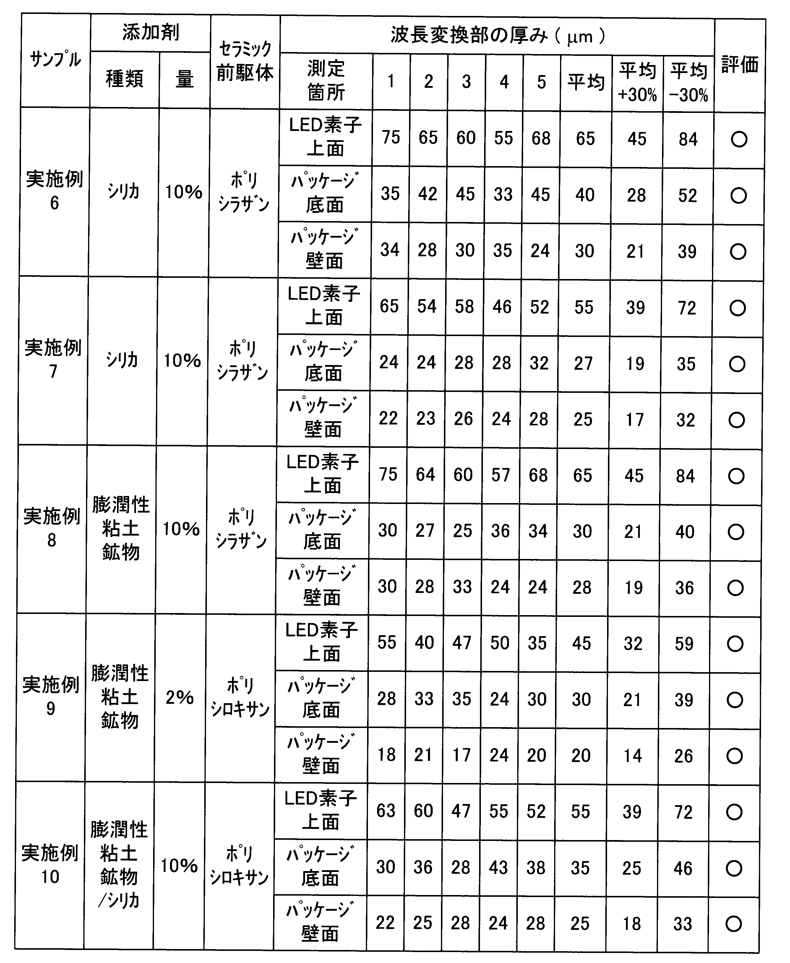
測定箇所として、LED素子上面、パッケージ底面およびパッケージ内壁面の3面を選択し、各面で5箇所ずつ膜厚を測定するとともに、その平均値を求めた。測定結果や算出した平均値を表1~表3(主には表1,表2)に示す。
なお、表中の添加剤の量(%)は波長変換部中の固形分中に占める添加剤の重量比(%)である。
表1~表3中、LED素子上面、パッケージ底面およびパッケージ内壁面それぞれにおいて、測定点のうち、5点すべてがその平均値±30%以内であれば厚みバラツキはないものと評価し(○)、1点でも平均値±30%の範囲に収まらなければ厚みバラツキがあると評価した(×)。
なお、LED素子上面の厚みに対するパッケージ内壁面の厚みの割合(%)も算出し、その結果を表3に示した。
(3.1)厚みの測定および厚みバラツキの評価
各サンプルにおいて、波長変換部の形成前後の高さ(差)を測定し、波長変換部の膜厚(厚み)を測定した。測定装置としてミツトヨ製測定顕微鏡MF-A505Hを用いた。
測定箇所として、LED素子上面、パッケージ底面およびパッケージ内壁面の3面を選択し、各面で5箇所ずつ膜厚を測定するとともに、その平均値を求めた。測定結果や算出した平均値を表1~表3(主には表1,表2)に示す。
なお、表中の添加剤の量(%)は波長変換部中の固形分中に占める添加剤の重量比(%)である。
表1~表3中、LED素子上面、パッケージ底面およびパッケージ内壁面それぞれにおいて、測定点のうち、5点すべてがその平均値±30%以内であれば厚みバラツキはないものと評価し(○)、1点でも平均値±30%の範囲に収まらなければ厚みバラツキがあると評価した(×)。
なお、LED素子上面の厚みに対するパッケージ内壁面の厚みの割合(%)も算出し、その結果を表3に示した。
(3.2)LED素子側面の露出部などの面積測定
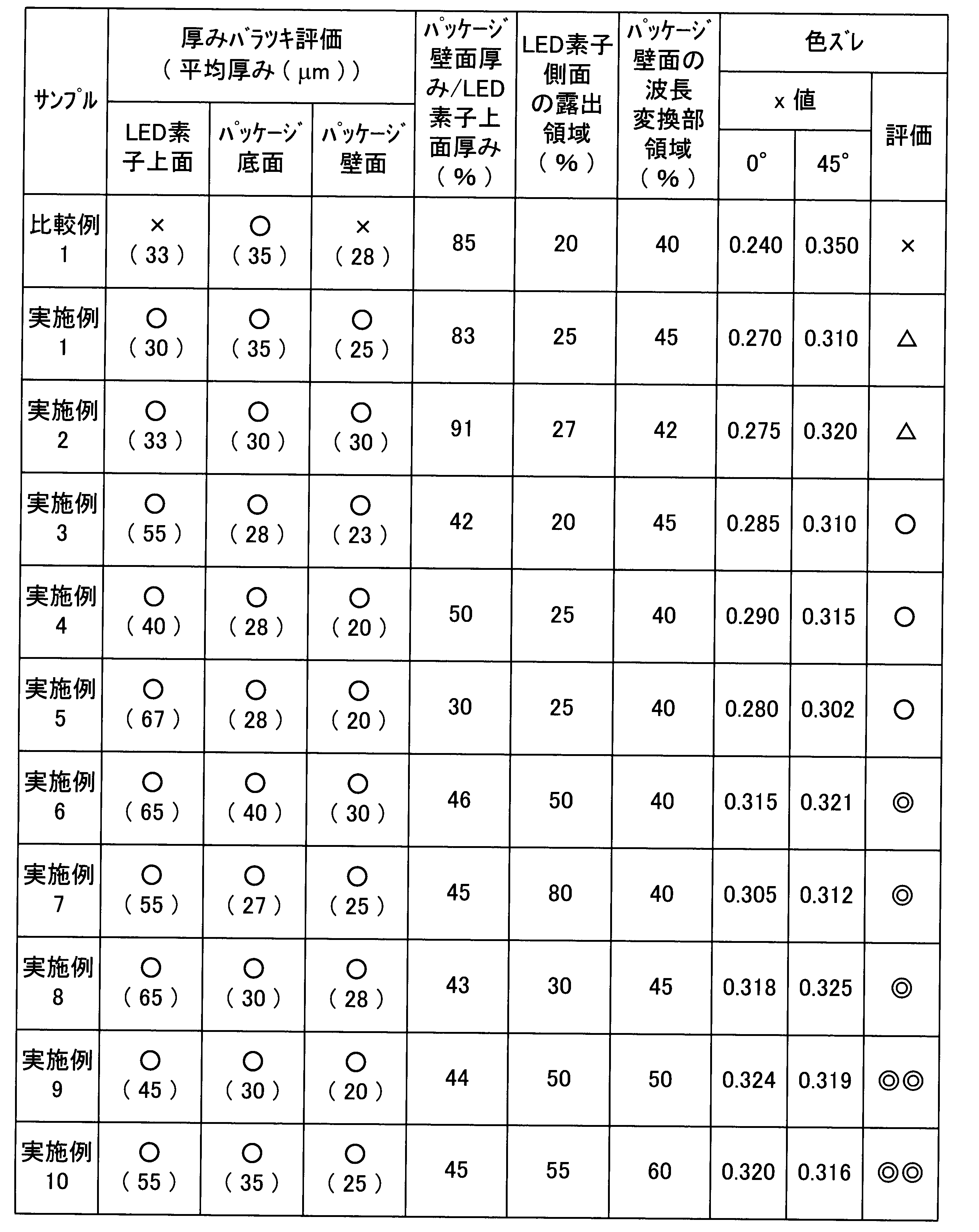
各サンプルにおいて、オリンパス製光学顕微鏡BX50を用いてLED素子の側面を観察し、露出部の面積を測定し、LED素子の全側面の面積に対する当該露出部の面積比(%)を算出した。併せて、パッケージ内壁面に形成した波長変換部の面積を測定し、パッケージの各内壁面の面積に対する当該波長変換部の面積比(%)も算出した。算出結果を表3に示す。
各サンプルにおいて、オリンパス製光学顕微鏡BX50を用いてLED素子の側面を観察し、露出部の面積を測定し、LED素子の全側面の面積に対する当該露出部の面積比(%)を算出した。併せて、パッケージ内壁面に形成した波長変換部の面積を測定し、パッケージの各内壁面の面積に対する当該波長変換部の面積比(%)も算出した。算出結果を表3に示す。
(3.3)色ズレの評価
測定装置としてコニカミノルタセンシング社製分光放射輝度計CS-1000Aを用いて、各サンプルからの発光色を測定した。測定はサンプルと測定装置との角度を0°,45°として行い、それぞれの角度での色度x値を測定した。
ここで色ズレがなければ異なる角度で測定しても色度x値は同様な値となる。
各角度での色度x値の差をサンプルごとに算出し、その算出値でサンプルの良否を判断した。評価結果を表3に示す。表3中、◎◎,◎,○,△,×の基準は下記のとおりである。
「×」…0.05より大きい
「△」…0.03より大きく、0.05以下である
「○」…0.01より大きく、0.03以下である
「◎」…0.005より大きく、0.01以下である
「◎◎」…0.005以下である
測定装置としてコニカミノルタセンシング社製分光放射輝度計CS-1000Aを用いて、各サンプルからの発光色を測定した。測定はサンプルと測定装置との角度を0°,45°として行い、それぞれの角度での色度x値を測定した。
ここで色ズレがなければ異なる角度で測定しても色度x値は同様な値となる。
各角度での色度x値の差をサンプルごとに算出し、その算出値でサンプルの良否を判断した。評価結果を表3に示す。表3中、◎◎,◎,○,△,×の基準は下記のとおりである。
「×」…0.05より大きい
「△」…0.03より大きく、0.05以下である
「○」…0.01より大きく、0.03以下である
「◎」…0.005より大きく、0.01以下である
「◎◎」…0.005以下である

(4)まとめ
表1~表3に示すとおり、比較例1と実施例1~10との各サンプルを比較すると、実施例1~10では結果が良好であった。このことから、色ズレの発生を抑制する上では、LED素子上面、パッケージ底面およびパッケージ内壁面のすべてにおいて、波長変換部の各部の厚みを平均値の±30%以内に収めることが有用であることがわかる。
実施例1~10のサンプルのなかでも、実施例3~10の結果が優れ、実施例6~8ではさらに結果が優れ、実施例9~10では結果が最良であった。これらのことから、色ズレの発生の抑制効果を向上させるには、パッケージ内壁面の波長変換部の厚みをLED素子上面の波長変換部の厚みの30~50%に制御することが有用であり、さらにはLED素子側面の露出部の面積比を30~80%に制御することや、パッケージ内壁面の面積に対する波長変換部の面積比を50%以上に制御することが有用であることがわかる。
表1~表3に示すとおり、比較例1と実施例1~10との各サンプルを比較すると、実施例1~10では結果が良好であった。このことから、色ズレの発生を抑制する上では、LED素子上面、パッケージ底面およびパッケージ内壁面のすべてにおいて、波長変換部の各部の厚みを平均値の±30%以内に収めることが有用であることがわかる。
実施例1~10のサンプルのなかでも、実施例3~10の結果が優れ、実施例6~8ではさらに結果が優れ、実施例9~10では結果が最良であった。これらのことから、色ズレの発生の抑制効果を向上させるには、パッケージ内壁面の波長変換部の厚みをLED素子上面の波長変換部の厚みの30~50%に制御することが有用であり、さらにはLED素子側面の露出部の面積比を30~80%に制御することや、パッケージ内壁面の面積に対する波長変換部の面積比を50%以上に制御することが有用であることがわかる。
本発明は色ズレの発生を抑制するのに好適に利用することができる。
2 パッケージ
2a 底面
2b 内壁面
4 LED素子
4a 上面
4b 側面
6 波長変換部
6a,6b,6c 波長変換部
10 塗布装置
20 移動台
30 スプレー装置
32 ノズル
34 連結管
36 タンク
40 第1の混合液
100 発光装置
2a 底面
2b 内壁面
4 LED素子
4a 上面
4b 側面
6 波長変換部
6a,6b,6c 波長変換部
10 塗布装置
20 移動台
30 スプレー装置
32 ノズル
34 連結管
36 タンク
40 第1の混合液
100 発光装置
Claims (5)
- 内壁面が傾斜した凹状のパッケージと、
前記パッケージの底面に配置された発光素子と、
前記発光素子の出射光を特定波長の光に変換する波長変換部と、
を備える発光装置において、
前記波長変換部が前記発光素子の上面、前記パッケージの底面および前記パッケージの内壁面に形成され、これら各面の前記波長変換部の厚みがすべて、その面の前記波長変換部の厚みの平均値に対して±30%の範囲内に収まっていることを特徴とする発光装置。 - 請求項1に記載の発光装置において、
前記パッケージの内壁面に形成された前記波長変換部の厚みが、前記発光素子の上面に形成された前記波長変換部の厚みの30~50%であることを特徴とする発光装置。 - 請求項2に記載の発光装置において、
前記発光素子の側面が、前記パッケージの底面と前記発光素子の上面とに形成された前記波長変換部の間から露出しており、
前記発光素子の側面の露出部の面積が、前記発光素子の側面のすべての面積の30~80%であることを特徴とする発光装置。 - 請求項3に記載の発光装置において、
前記パッケージの内壁面に形成された前記波長変換部のその内壁面に占める面積比が50%以上であることを特徴とする発光装置。 - 内壁面が傾斜した凹状のパッケージと、
前記パッケージの底面に配置された発光素子と、
前記発光素子の出射光を特定波長の光に変換する波長変換部と、
を備える発光装置の製造方法において、
蛍光体と、膨潤性粒子または無機粒子の少なくとも一方とを、水または有機溶媒の少なくとも一方に分散し、第1の混合液を調製する工程と、
前記第1の混合液を、前記発光素子を実装した前記パッケージ上に塗布して加熱し、前記発光素子の上面、前記パッケージの底面および前記パッケージの内壁面に対し、前記波長変換部の前駆体を形成する工程と、
透光性のセラミック前駆体を溶媒に分散した第2の混合液を、前記波長変換部の前駆体上に塗布して加熱し、前記波長変換部を形成する工程と、
を有することを特徴とする発光装置の製造方法。
Priority Applications (1)
| Application Number | Priority Date | Filing Date | Title |
|---|---|---|---|
| JP2012550953A JP5803940B2 (ja) | 2010-12-27 | 2011-12-26 | 発光装置およびその製造方法 |
Applications Claiming Priority (2)
| Application Number | Priority Date | Filing Date | Title |
|---|---|---|---|
| JP2010289548 | 2010-12-27 | ||
| JP2010-289548 | 2010-12-27 |
Publications (1)
| Publication Number | Publication Date |
|---|---|
| WO2012090966A1 true WO2012090966A1 (ja) | 2012-07-05 |
Family
ID=46383066
Family Applications (1)
| Application Number | Title | Priority Date | Filing Date |
|---|---|---|---|
| PCT/JP2011/080131 Ceased WO2012090966A1 (ja) | 2010-12-27 | 2011-12-26 | 発光装置およびその製造方法 |
Country Status (2)
| Country | Link |
|---|---|
| JP (1) | JP5803940B2 (ja) |
| WO (1) | WO2012090966A1 (ja) |
Cited By (4)
| Publication number | Priority date | Publication date | Assignee | Title |
|---|---|---|---|---|
| JP2014072309A (ja) * | 2012-09-28 | 2014-04-21 | Stanley Electric Co Ltd | 自動車ヘッドランプ用発光装置及びその製造方法 |
| JP2016071271A (ja) * | 2014-10-01 | 2016-05-09 | コニカミノルタ株式会社 | 照明用発光装置および画像読取装置 |
| US9825012B2 (en) | 2012-08-15 | 2017-11-21 | Epistar Corporation | Light-emitting device |
| US11791370B2 (en) | 2012-08-15 | 2023-10-17 | Epistar Corporation | Light-emitting device |
Citations (4)
| Publication number | Priority date | Publication date | Assignee | Title |
|---|---|---|---|---|
| JP2001181614A (ja) * | 1999-12-24 | 2001-07-03 | Teikoku Tsushin Kogyo Co Ltd | El素子用蛍光体ペースト及びその製造方法 |
| JP2002134795A (ja) * | 2000-10-27 | 2002-05-10 | Sanken Electric Co Ltd | 半導体発光装置及びその製法 |
| JP2008135539A (ja) * | 2006-11-28 | 2008-06-12 | Dowa Electronics Materials Co Ltd | 発光装置及びその製造方法 |
| JP2009094262A (ja) * | 2007-10-09 | 2009-04-30 | Toyoda Gosei Co Ltd | 発光装置の製造方法 |
-
2011
- 2011-12-26 WO PCT/JP2011/080131 patent/WO2012090966A1/ja not_active Ceased
- 2011-12-26 JP JP2012550953A patent/JP5803940B2/ja not_active Expired - Fee Related
Patent Citations (4)
| Publication number | Priority date | Publication date | Assignee | Title |
|---|---|---|---|---|
| JP2001181614A (ja) * | 1999-12-24 | 2001-07-03 | Teikoku Tsushin Kogyo Co Ltd | El素子用蛍光体ペースト及びその製造方法 |
| JP2002134795A (ja) * | 2000-10-27 | 2002-05-10 | Sanken Electric Co Ltd | 半導体発光装置及びその製法 |
| JP2008135539A (ja) * | 2006-11-28 | 2008-06-12 | Dowa Electronics Materials Co Ltd | 発光装置及びその製造方法 |
| JP2009094262A (ja) * | 2007-10-09 | 2009-04-30 | Toyoda Gosei Co Ltd | 発光装置の製造方法 |
Cited By (10)
| Publication number | Priority date | Publication date | Assignee | Title |
|---|---|---|---|---|
| US9825012B2 (en) | 2012-08-15 | 2017-11-21 | Epistar Corporation | Light-emitting device |
| US10083945B2 (en) | 2012-08-15 | 2018-09-25 | Epistar Corporation | Light-emitting device |
| US10319703B2 (en) | 2012-08-15 | 2019-06-11 | Epistar Corporation | Light bulb |
| US10593655B2 (en) | 2012-08-15 | 2020-03-17 | Epistar Corporation | Light bulb |
| US10720414B2 (en) | 2012-08-15 | 2020-07-21 | Epistar Corporation | Light bulb |
| US10886262B2 (en) | 2012-08-15 | 2021-01-05 | Epistar Corporation | Light bulb |
| US11791370B2 (en) | 2012-08-15 | 2023-10-17 | Epistar Corporation | Light-emitting device |
| US12132073B2 (en) | 2012-08-15 | 2024-10-29 | Epistar Corporation | Light-emitting device |
| JP2014072309A (ja) * | 2012-09-28 | 2014-04-21 | Stanley Electric Co Ltd | 自動車ヘッドランプ用発光装置及びその製造方法 |
| JP2016071271A (ja) * | 2014-10-01 | 2016-05-09 | コニカミノルタ株式会社 | 照明用発光装置および画像読取装置 |
Also Published As
| Publication number | Publication date |
|---|---|
| JP5803940B2 (ja) | 2015-11-04 |
| JPWO2012090966A1 (ja) | 2014-06-05 |
Similar Documents
| Publication | Publication Date | Title |
|---|---|---|
| JP5870923B2 (ja) | 発光装置の製造方法 | |
| JP5999223B2 (ja) | 発光装置の製造方法および蛍光体混合液 | |
| US20150004728A1 (en) | Led device manufacturing method and fluorescent material-dispersed solution used in same | |
| JP2011238811A (ja) | 波長変換素子および発光装置 | |
| US20110278616A1 (en) | Manufacturing method of wavelength conversion element, wavelength conversion element, and light emitting device | |
| JPWO2013051280A1 (ja) | 蛍光体分散液、及びこれを用いたled装置の製造方法 | |
| JP6076909B2 (ja) | 蛍光体分散液、およびled装置の製造方法 | |
| JP5869769B2 (ja) | 蛍光体層の形成方法および発光装置の製造方法 | |
| JP5803541B2 (ja) | Led装置およびその製造方法、並びにそれに用いる蛍光体分散液 | |
| JP5803940B2 (ja) | 発光装置およびその製造方法 | |
| JPWO2012067200A1 (ja) | 波長変換素子及びその製造方法、発光装置及びその製造方法 | |
| JP5880566B2 (ja) | Led装置 | |
| JP5747994B2 (ja) | 波長変換素子及びその製造方法、発光装置及びその製造方法 | |
| JP2012004475A (ja) | 反りを抑えた基板、それを用いた発光装置及びそれらの製造方法 | |
| JPWO2012090961A1 (ja) | 発光装置、発光装置の製造方法、及び、塗布液 | |
| JP2013165223A (ja) | 波長変換素子及びその製造方法、発光装置及びその製造方法、蛍光体分散液 | |
| JP5765428B2 (ja) | Led装置の製造方法 | |
| JP5803941B2 (ja) | 発光装置の製造方法 | |
| JP2012195522A (ja) | 発光装置の製造方法 | |
| JP2013258339A (ja) | 発光装置及びその製造方法 |
Legal Events
| Date | Code | Title | Description |
|---|---|---|---|
| 121 | Ep: the epo has been informed by wipo that ep was designated in this application |
Ref document number: 11854521 Country of ref document: EP Kind code of ref document: A1 |
|
| ENP | Entry into the national phase |
Ref document number: 2012550953 Country of ref document: JP Kind code of ref document: A |
|
| NENP | Non-entry into the national phase |
Ref country code: DE |
|
| 122 | Ep: pct application non-entry in european phase |
Ref document number: 11854521 Country of ref document: EP Kind code of ref document: A1 |