WO2012090636A1 - 光電変換素子および光電変換素子の製造方法 - Google Patents
光電変換素子および光電変換素子の製造方法 Download PDFInfo
- Publication number
- WO2012090636A1 WO2012090636A1 PCT/JP2011/077614 JP2011077614W WO2012090636A1 WO 2012090636 A1 WO2012090636 A1 WO 2012090636A1 JP 2011077614 W JP2011077614 W JP 2011077614W WO 2012090636 A1 WO2012090636 A1 WO 2012090636A1
- Authority
- WO
- WIPO (PCT)
- Prior art keywords
- nitride semiconductor
- type nitride
- photoelectric conversion
- conversion element
- semiconductor layer
- Prior art date
- Legal status (The legal status is an assumption and is not a legal conclusion. Google has not performed a legal analysis and makes no representation as to the accuracy of the status listed.)
- Ceased
Links
Images






Classifications
-
- H—ELECTRICITY
- H10—SEMICONDUCTOR DEVICES; ELECTRIC SOLID-STATE DEVICES NOT OTHERWISE PROVIDED FOR
- H10F—INORGANIC SEMICONDUCTOR DEVICES SENSITIVE TO INFRARED RADIATION, LIGHT, ELECTROMAGNETIC RADIATION OF SHORTER WAVELENGTH OR CORPUSCULAR RADIATION
- H10F77/00—Constructional details of devices covered by this subclass
- H10F77/70—Surface textures, e.g. pyramid structures
- H10F77/703—Surface textures, e.g. pyramid structures of the semiconductor bodies, e.g. textured active layers
-
- B—PERFORMING OPERATIONS; TRANSPORTING
- B82—NANOTECHNOLOGY
- B82Y—SPECIFIC USES OR APPLICATIONS OF NANOSTRUCTURES; MEASUREMENT OR ANALYSIS OF NANOSTRUCTURES; MANUFACTURE OR TREATMENT OF NANOSTRUCTURES
- B82Y20/00—Nanooptics, e.g. quantum optics or photonic crystals
-
- H—ELECTRICITY
- H10—SEMICONDUCTOR DEVICES; ELECTRIC SOLID-STATE DEVICES NOT OTHERWISE PROVIDED FOR
- H10F—INORGANIC SEMICONDUCTOR DEVICES SENSITIVE TO INFRARED RADIATION, LIGHT, ELECTROMAGNETIC RADIATION OF SHORTER WAVELENGTH OR CORPUSCULAR RADIATION
- H10F10/00—Individual photovoltaic cells, e.g. solar cells
- H10F10/10—Individual photovoltaic cells, e.g. solar cells having potential barriers
- H10F10/17—Photovoltaic cells having only PIN junction potential barriers
-
- H—ELECTRICITY
- H10—SEMICONDUCTOR DEVICES; ELECTRIC SOLID-STATE DEVICES NOT OTHERWISE PROVIDED FOR
- H10F—INORGANIC SEMICONDUCTOR DEVICES SENSITIVE TO INFRARED RADIATION, LIGHT, ELECTROMAGNETIC RADIATION OF SHORTER WAVELENGTH OR CORPUSCULAR RADIATION
- H10F77/00—Constructional details of devices covered by this subclass
- H10F77/10—Semiconductor bodies
- H10F77/12—Active materials
- H10F77/124—Active materials comprising only Group III-V materials, e.g. GaAs
- H10F77/1248—Active materials comprising only Group III-V materials, e.g. GaAs having three or more elements, e.g. GaAlAs, InGaAs or InGaAsP
- H10F77/12485—Active materials comprising only Group III-V materials, e.g. GaAs having three or more elements, e.g. GaAlAs, InGaAs or InGaAsP comprising nitride compounds, e.g. InGaN
-
- H—ELECTRICITY
- H10—SEMICONDUCTOR DEVICES; ELECTRIC SOLID-STATE DEVICES NOT OTHERWISE PROVIDED FOR
- H10F—INORGANIC SEMICONDUCTOR DEVICES SENSITIVE TO INFRARED RADIATION, LIGHT, ELECTROMAGNETIC RADIATION OF SHORTER WAVELENGTH OR CORPUSCULAR RADIATION
- H10F77/00—Constructional details of devices covered by this subclass
- H10F77/10—Semiconductor bodies
- H10F77/14—Shape of semiconductor bodies; Shapes, relative sizes or dispositions of semiconductor regions within semiconductor bodies
- H10F77/146—Superlattices; Multiple quantum well structures
-
- H—ELECTRICITY
- H10—SEMICONDUCTOR DEVICES; ELECTRIC SOLID-STATE DEVICES NOT OTHERWISE PROVIDED FOR
- H10F—INORGANIC SEMICONDUCTOR DEVICES SENSITIVE TO INFRARED RADIATION, LIGHT, ELECTROMAGNETIC RADIATION OF SHORTER WAVELENGTH OR CORPUSCULAR RADIATION
- H10F77/00—Constructional details of devices covered by this subclass
- H10F77/20—Electrodes
- H10F77/206—Electrodes for devices having potential barriers
- H10F77/211—Electrodes for devices having potential barriers for photovoltaic cells
-
- Y—GENERAL TAGGING OF NEW TECHNOLOGICAL DEVELOPMENTS; GENERAL TAGGING OF CROSS-SECTIONAL TECHNOLOGIES SPANNING OVER SEVERAL SECTIONS OF THE IPC; TECHNICAL SUBJECTS COVERED BY FORMER USPC CROSS-REFERENCE ART COLLECTIONS [XRACs] AND DIGESTS
- Y02—TECHNOLOGIES OR APPLICATIONS FOR MITIGATION OR ADAPTATION AGAINST CLIMATE CHANGE
- Y02E—REDUCTION OF GREENHOUSE GAS [GHG] EMISSIONS, RELATED TO ENERGY GENERATION, TRANSMISSION OR DISTRIBUTION
- Y02E10/00—Energy generation through renewable energy sources
- Y02E10/50—Photovoltaic [PV] energy
- Y02E10/544—Solar cells from Group III-V materials
-
- Y—GENERAL TAGGING OF NEW TECHNOLOGICAL DEVELOPMENTS; GENERAL TAGGING OF CROSS-SECTIONAL TECHNOLOGIES SPANNING OVER SEVERAL SECTIONS OF THE IPC; TECHNICAL SUBJECTS COVERED BY FORMER USPC CROSS-REFERENCE ART COLLECTIONS [XRACs] AND DIGESTS
- Y02—TECHNOLOGIES OR APPLICATIONS FOR MITIGATION OR ADAPTATION AGAINST CLIMATE CHANGE
- Y02E—REDUCTION OF GREENHOUSE GAS [GHG] EMISSIONS, RELATED TO ENERGY GENERATION, TRANSMISSION OR DISTRIBUTION
- Y02E10/00—Energy generation through renewable energy sources
- Y02E10/50—Photovoltaic [PV] energy
- Y02E10/548—Amorphous silicon PV cells
-
- Y—GENERAL TAGGING OF NEW TECHNOLOGICAL DEVELOPMENTS; GENERAL TAGGING OF CROSS-SECTIONAL TECHNOLOGIES SPANNING OVER SEVERAL SECTIONS OF THE IPC; TECHNICAL SUBJECTS COVERED BY FORMER USPC CROSS-REFERENCE ART COLLECTIONS [XRACs] AND DIGESTS
- Y02—TECHNOLOGIES OR APPLICATIONS FOR MITIGATION OR ADAPTATION AGAINST CLIMATE CHANGE
- Y02P—CLIMATE CHANGE MITIGATION TECHNOLOGIES IN THE PRODUCTION OR PROCESSING OF GOODS
- Y02P70/00—Climate change mitigation technologies in the production process for final industrial or consumer products
- Y02P70/50—Manufacturing or production processes characterised by the final manufactured product
Definitions
- the present invention relates to a photoelectric conversion element and a method for manufacturing the photoelectric conversion element.
- photoelectric conversion elements are generally made of silicon (for example, amorphous silicon, microcrystalline silicon, or polycrystalline silicon).
- silicon for example, amorphous silicon, microcrystalline silicon, or polycrystalline silicon.
- the band gap of silicon is 1.1 eV to 1.8 eV, there is a problem that the sensitivity to light in a short wavelength region with a high energy of 0.5 ⁇ m or less is small and sunlight cannot be effectively used. .
- the band gap of the nitride semiconductor represented by the formula of Al x In y Ga (1-xy) N (0 ⁇ x ⁇ 1, 0 ⁇ y ⁇ 1, 0 ⁇ x + y ⁇ 1) has been discussed for a long time.
- the nitride semiconductor is generally formed by vapor deposition such as metal organic chemical vapor deposition (MOCVD), hydride vapor deposition (HVPE), molecular beam vapor deposition (MBE), or pulsed laser deposition (PLD). It can be formed on a substrate using a phase growth method.
- MOCVD metal organic chemical vapor deposition
- HVPE hydride vapor deposition
- MBE molecular beam vapor deposition
- PLD pulsed laser deposition
- nitride semiconductor is suitable as a material for a light emitting element such as a light emitting diode (LED), it has been actively developed.
- a light emitting element such as a light emitting diode (LED)
- LED light emitting diode
- research on forming a nitride semiconductor using a vapor phase growth method as a material for a next-generation photoelectric conversion element has been actively conducted by elucidating the band gap of the nitride semiconductor.
- Patent Document 1 Japanese Patent Laid-Open No. 7-288334
- Patent Document 2 US Patent Application Publication No. 2004/0118451
- Patent Document 3 US Pat. No. 7,217,882
- generating a large number of photocarriers means increasing the short-circuit current. Therefore, for the purpose of improving the characteristics of the photoelectric conversion element, the photoelectric conversion element using a nitride semiconductor can be activated by the active layer of the photoelectric conversion element. It is desired to generate a large number of carriers.
- an object of the present invention is to provide a photoelectric conversion element capable of improving characteristics and a method for manufacturing the photoelectric conversion element.
- the present invention includes a substrate, a semiconductor stacked body provided on the substrate, and a conductive layer provided on the semiconductor stacked body, and the semiconductor stacked body includes a p-type nitride semiconductor layer and an i-type nitride semiconductor.
- the semiconductor stack includes a pin structure having a layer and an n-type nitride semiconductor layer, and the semiconductor stack is a photoelectric conversion element having irregularities at the interface on the conductive layer side of the semiconductor stack.
- the unevenness has a plurality of linear grooves arranged at intervals, and the depth of the grooves is 0.5 ⁇ m or more and 3 ⁇ m or less.
- the width is 0.35 ⁇ m or more and 1 ⁇ m or less
- the interval is 0.35 ⁇ m or more and 1 ⁇ m or less
- the width of the groove is preferably equal to or less than the above-described interval.
- the pin structure includes an n-type nitride semiconductor layer on the substrate side, a p-type nitride semiconductor layer on the conductive layer side, and the n-type nitride semiconductor layer.
- An i-type nitride semiconductor layer is preferably provided between the p-type nitride semiconductor layer and the p-type nitride semiconductor layer.
- the surface roughness RMS of the surface of the conductive layer opposite to the uneven side is preferably 0.003 ⁇ m or more and 0.005 ⁇ m or less.
- the thickness of the conductive layer is preferably 0.25 ⁇ m or more and 0.5 ⁇ m or less.
- the conductive layer preferably has a refractive index smaller than that of the p-type nitride semiconductor layer.
- the conductive layer is preferably a single layer including at least one selected from the group consisting of Zn, In, Sn, and Mg, or a multiple layer in which a plurality of single layers are stacked. .
- the substrate is made of Al x In y Ga z N (0 ⁇ x ⁇ 1, 0 ⁇ y ⁇ 1, 0 ⁇ z ⁇ 1, x + y + z ⁇ 0), GaP, GaAs, NdGaO 3. , LiGaO 2 , Al 2 O 3 , MgAl 2 O 4 , ZnO, Si, SiC, SiGe, or a material represented by the formula ZrB 2 is preferably included.
- the present invention is a method for manufacturing any one of the above photoelectric conversion elements, the step of forming a semiconductor stacked body on a substrate, the step of forming irregularities on the semiconductor stacked body, Forming a conductive layer, and forming the irregularities by at least one selected from the group consisting of laser light irradiation, RIE, dry etching, and plasma CVM. .
- the present invention it is possible to provide a photoelectric conversion element capable of improving characteristics and a method for manufacturing the photoelectric conversion element.
- FIG. 1 is a schematic cross-sectional view of a photoelectric conversion element according to an embodiment which is an example of the photoelectric conversion element of the present invention.
- the photoelectric conversion element of the embodiment includes a substrate 1, a semiconductor stacked body 12 provided on the substrate 1, and a conductive layer 5 provided on the semiconductor stacked body 12.
- the semiconductor stacked body 12 has a pin structure in which an n-type nitride semiconductor layer 2, an i-type nitride semiconductor layer 3, and a p-type nitride semiconductor layer 4 are stacked in this order from the substrate 1 side. is doing.
- the pin structure includes an n-type nitride semiconductor layer 2 on the substrate 1 side and a p-type nitride semiconductor layer 4 on the conductive layer 5 side.
- the n-type nitride semiconductor layer 2 and the p-type nitride are included in the pin structure.
- An i-type nitride semiconductor layer 3 is provided between the semiconductor layer 4 and the semiconductor layer 4.
- the n-type nitride semiconductor layer 2 and the i-type nitride semiconductor layer 3 are in contact with each other, and the i-type nitride semiconductor layer 3 and the p-type nitride semiconductor layer 4 are in contact with each other. It is constituted by.
- n pad electrode 6 is formed on the surface of the n-type nitride semiconductor layer 2, and a p pad electrode 7 is formed on the surface of the conductive layer 5.
- the n pad electrode 6 and the p pad electrode 7 do not have to be installed, but are preferably installed.
- the semiconductor laminate 12 has irregularities 11 at the interface on the conductive layer 5 side of the semiconductor laminate 12.
- the unevenness 11 includes a plurality of linear grooves 8 extending on the front surface and / or the back surface of the paper surface of FIG. And the adjacent groove
- the light that has entered the semiconductor stacked body 12 from the conductive layer 5 side and is not absorbed by the i-type nitride semiconductor layer 3 but returned to the p-type nitride semiconductor layer 4 side Multiple reflections can be made by the grooves 8 of the unevenness 11 and the light can enter the i-type nitride semiconductor layer 3 again.
- the optical path length in the i-type nitride semiconductor layer 3 serving as a photoelectric conversion layer can be increased, and therefore, photocarriers generated by light absorption in the i-type nitride semiconductor layer 3 are increased. Can do.
- a photoelectric conversion element having high characteristics can be obtained.
- FIG. 2 is a schematic enlarged cross-sectional view of the vicinity of the unevenness 11 of the photoelectric conversion element of the embodiment.
- the depth d of the groove 8 is preferably 0.5 ⁇ m or more and 3 ⁇ m or less, and more preferably 0.8 ⁇ m or more and 1.5 ⁇ m or less.
- the depth d of the groove 8 is 0.5 ⁇ m or more and 3 ⁇ m or less, particularly when the depth d is 0.8 ⁇ m or more and 1.5 ⁇ m or less, the multiple reflection on the irregularities 11 of the light once incident on the semiconductor laminate 12 is promoted.
- the optical confinement in the semiconductor stacked body 12 tends to be further effective, and the deterioration of the characteristics due to the step coverage on the surface of the p-type nitride semiconductor layer 4 tends to be suppressed. Thereby, it exists in the tendency which can improve the characteristic of a photoelectric conversion element.
- the width l of the groove 8 is preferably 0.35 ⁇ m or more and 1 ⁇ m or less.
- the width l of the groove 8 is not less than 0.35 ⁇ m and not more than 1 ⁇ m, the multiple reflection at the irregularities 11 of the light once incident on the semiconductor stacked body 12 is promoted to make the optical confinement in the semiconductor stacked body 12 more effective. Therefore, the characteristics of the photoelectric conversion element tend to be higher.
- the interval L between adjacent grooves 8 is preferably 0.35 ⁇ m or more and 1 ⁇ m or less.
- the interval L between the grooves 8 is not less than 0.35 ⁇ m and not more than 1 ⁇ m, the multiple reflection at the irregularities 11 of the light once incident on the semiconductor stacked body 12 is promoted to make the optical confinement in the semiconductor stacked body 12 more effective. Therefore, the characteristics of the photoelectric conversion element tend to be higher.
- the method for measuring the depth d, width l, and interval L of the groove 8 is not particularly limited.
- measurement using an atomic force microscope (AFM) or a contact-type step measuring instrument is used. Measurement can be used.
- the surface roughness RMS (mean square error) of the surface 5a opposite to the side having the irregularities 11 of the conductive layer 5 is preferably 0.003 ⁇ m or more and 0.005 ⁇ m or less.
- the surface roughness RMS of the surface 5a of the conductive layer 5 is 0.003 ⁇ m or more and 0.005 ⁇ m or less.
- the surface roughness RMS of the surface 5a of the conductive layer 5 can be calculated by measuring an arbitrary square region having a side of 40 ⁇ m on the surface 5a using an atomic force microscope.
- the thickness t of the conductive layer 5 is preferably 0.25 ⁇ m or more and 0.5 ⁇ m or less.
- the conductive layer 5 can form good ohmic contact with the surface of the p-type nitride semiconductor layer 4 on the unevenness 11 side. Therefore, F.A.
- F (fill factor) There is a tendency that the characteristics of the photoelectric conversion element can be further improved by suppressing a decrease in F (fill factor).
- the thickness t of the conductive layer 5 is 0.25 ⁇ m or more and 0.5 ⁇ m or less, the sensitivity to light in a short wavelength region of 0.4 ⁇ m or more and 0.5 ⁇ m or less is increased, and the above-described unevenness 11 is multiplexed.
- the amount of photocarriers generated in the i-type nitride semiconductor layer 3 can be increased by a synergistic effect with an increase in the light confinement effect due to reflection. Thereby, since the amount of short circuit current can be increased, it exists in the tendency which can make the characteristic of a photoelectric conversion element higher.
- the conductive layer 5 preferably has a smaller refractive index than the p-type nitride semiconductor layer 4.
- the refractive index of the conductive layer 5 is smaller than the refractive index of the p-type nitride semiconductor layer 4, the amount of reflection of light incident from the conductive layer 5 at the interface between the conductive layer 5 and the p-type nitride semiconductor layer 4 is calculated.
- the amount of incident light into the p-type nitride semiconductor layer 4 can be reduced and the amount of photocarriers generated in the i-type nitride semiconductor layer 3 can be increased. Thereby, since the amount of short circuit current can be increased, it exists in the tendency which can make the characteristic of a photoelectric conversion element higher.
- the refractive index of the p-type nitride semiconductor layer 4 is 2.3, for example, it is preferable to use a material having a refractive index smaller than 2.3 as the conductive layer 5.
- the refractive index means an absolute refractive index.
- FIG. 3 shows a schematic enlarged plan view of the unevenness 11 of the photoelectric conversion element of the embodiment.
- the unevenness 11 of the photoelectric conversion element according to the embodiment has stripe-like grooves 8 in which linear grooves 8 having a width l are periodically arranged at intervals L.
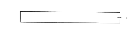
- a substrate 1 is prepared.
- Al x In y Ga z N (0 ⁇ x ⁇ 1,0 ⁇ y ⁇ 1,0 ⁇ z ⁇ 1, x + y + z ⁇ 0)
- GaP GaAs, NdGaO 3, LiGaO 2, Al 2 O 3 , MgAl 2 O 4 , ZnO, Si, SiC, SiGe, or a substrate having at least a material represented by the formula ZrB 2 is preferably used.
- the n-type nitride semiconductor layer 2 and the i-type nitride are formed.
- the semiconductor stacked body 12 can be formed by stacking the physical semiconductor layer 3 and the p-type nitride semiconductor layer 4 by vapor phase growth.
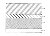
- an n-type nitride semiconductor layer 2 is stacked on the surface of the substrate 1.
- the n-type nitride semiconductor layer 2 can be laminated by, for example, MOCVD (Metal Organic Chemical Vapor Deposition) method.
- N-type nitride semiconductor layer 2 can be stacked with a thickness of 0.1 ⁇ m or more and 4 ⁇ m or less, for example.
- n-type nitride semiconductor layer 2 for example, a nitride semiconductor represented by the formula of Al x1 In y1 Ga z1 N (0 ⁇ x1 ⁇ 1, 0 ⁇ y1 ⁇ 1, 0 ⁇ z1 ⁇ 1, x1 + y1 + z1 ⁇ 0)
- a material doped with an n-type dopant can be used.
- silicon or the like can be used as the n-type dopant.
- the i-type nitride semiconductor layer 3 is laminated on the surface of the n-type nitride semiconductor layer 2.
- the i-type nitride semiconductor layer 3 can be laminated by, for example, the MOCVD method.
- i-type nitride semiconductor layer 3 can be laminated with a thickness of 0.001 ⁇ m or more and 0.3 ⁇ m or less, for example.
- a layer having an SQW (Single Quantum Well) structure or an MQW (Multiple Quantum Well) structure can be used as the i-type nitride semiconductor layer 3.
- the i-type nitride semiconductor layer 3 having the MQW structure is represented by, for example, an expression of Al x2 In y2 Ga z2 N (0 ⁇ x2 ⁇ 1, 0 ⁇ y2 ⁇ 1, 0 ⁇ z2 ⁇ 1, x2 + y2 + z2 ⁇ 0).
- a layer in which barrier layers are alternately stacked can be used.
- the well layer and / or the barrier layer may be doped with an n-type dopant and / or a p-type dopant.
- the thickness of the well layer can be, for example, 0.001 ⁇ m or more and 0.02 ⁇ m or less
- the thickness of the barrier layer can be, for example, 0.001 ⁇ m or more and 0.01 ⁇ m or less.
- a p-type nitride semiconductor layer 4 is stacked on the surface of the i-type nitride semiconductor layer 3.
- the p-type nitride semiconductor layer 4 can be laminated by, for example, the MOCVD method.
- the p-type nitride semiconductor layer 4 can be laminated with a thickness of 0.05 ⁇ m or more and 4 ⁇ m or less, for example.
- a material doped with a p-type dopant can be used.
- magnesium etc. can be used, for example.
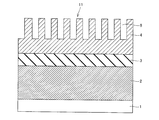
- irregularities 11 are formed on the surface of the p-type nitride semiconductor layer 4.
- the method for forming the irregularities 11 is not particularly limited, but for example, at least one selected from the group consisting of laser light irradiation, reactive ion etching (RIE), dry etching, and plasma CVM (Chemical Vaporization Machining) Can be formed.
- RIE reactive ion etching
- CVM Chemical Vaporization Machining
- the grooves 8 of the irregularities 11 tend to be formed more efficiently.
- laser light for example, the fundamental wave, second harmonic, or third harmonic of YAG laser light can be used.
- a conductive layer 5 is formed on the surface of the p-type nitride semiconductor layer 4.
- the method for forming the conductive layer 5 is not particularly limited, but can be formed by a sputtering method such as a magnetron sputtering method, a vacuum deposition method, or an ion plating method, for example.
- the conductive layer 5 it is preferable to use a magnetron sputtering method.
- the surface 5a of the conductive layer 5 on the side opposite to the unevenness 11 side tends to be flatter.
- the depth d of the groove 8 is less than 2 ⁇ m and the thickness t of the conductive layer 5 is 0.05 ⁇ m or more
- the surface 5a of the conductive layer 5 has excellent step coverage,
- the surface roughness RMS of the surface 5a tends to be 0.003 ⁇ m or more and 0.005 ⁇ m or less.
- a conductive material can be used, and when light is incident from the conductive layer 5 side, a material capable of transmitting incident light is preferably used.
- the conductive layer 5 it is preferable to use a single layer including at least one selected from the group consisting of Zn, In, Sn, and Mg, or a plurality of layers in which a plurality of single layers are stacked. In this case, the amount of light transmitted through the conductive layer 5 tends to be increased.
- the single layer containing Zn includes, for example, an AZO (Aluminum doped Zinc Oxide) layer in which Zn is doped with Al, a GZO (Gallium doped Zinc Oxide) layer in which ZnO is doped with Ga, and ZnO is doped with Mg.
- an MZO (Magnesium doped Zinc Oxide) layer, an IZO (Indium doped Zinc Oxide) layer in which Zn is doped with In, or the like can be given.
- Examples of the single layer containing In and the single layer containing Sn include ITO (Indium Tin Oxide) which is a composite oxide of In and Sn.
- Examples of the single layer containing Mg include Mg (OH) 2 doped with carbon (C).
- AZO formed by magnetron sputtering using a ZnO target doped with Al and having a partial pressure of oxygen and argon (O 2 / Ar) of 3% to 10% has a conductivity and a light It can be set as the conductive layer 5 excellent in the transmittance
- the n-type nitride semiconductor layer 2, the i-type nitride semiconductor layer 3, the p-type nitride semiconductor layer 4, and the conductive layer until the surface of the n-type nitride semiconductor layer 2 is exposed. A part of each of 5 is removed by etching.
- the n-pad electrode 6 and the p-pad electrode 7 are formed on the exposed surface of the n-type nitride semiconductor layer 2 and the surface of the conductive layer 5, respectively. Can be manufactured.
- FIG. 11 is a schematic enlarged cross-sectional view of another example of the groove 8 of the photoelectric conversion element of the embodiment.
- the groove 8 shown in FIG. 11 is characterized in that the bottom surface of the linear groove 8 extending on the front surface and / or back surface of FIG. 11 is a curved surface. Also in this case, the same effect as the groove 8 shown in FIG. 1 in which the bottom surface of the groove 8 is a flat surface can be obtained.
- the width l of the groove 8 shown in FIG. 11 means the width at the opening of the groove 8, and the depth d of the groove 8 is the shortest distance between the opening of the groove 8 and the deepest part of the bottom surface of the groove 8. means.
- FIG. 12 shows a schematic enlarged sectional view of another example of the groove 8 of the photoelectric conversion element of the embodiment.
- the groove 8 shown in FIG. 12 is characterized in that the cross-sectional shape of the linear groove 8 extending on the front surface and / or back surface of FIG. 12 is trapezoidal. Also in this case, the same effect as the groove 8 shown in FIG. 1 in which the cross-sectional shape of the groove 8 is a square shape can be obtained.
- the width l of the groove 8 shown in FIG. 12 means the width at a position where the length from the bottom surface of the groove 8 to the upper side of the groove 8 is d / 2 with respect to the bottom surface of the groove 8.
- the angle ⁇ formed by the bottom surface 8a and the side surface 8b of the groove 8 shown in FIG. 12 is preferably 100 ° or more and 160 ° or less.
- the angle ⁇ is not less than 100 ° and not more than 160 °, the light traveling from the p-type nitride semiconductor layer 4 to the conductive layer 5 is totally reflected at the interface between the p-type nitride semiconductor layer 4 and the conductive layer 5. Therefore, the characteristics of the photoelectric conversion element can be further enhanced.
- FIG. 13 is a schematic enlarged cross-sectional view of another example of the groove 8 of the photoelectric conversion element of the embodiment.
- the groove 8 shown in FIG. 13 is characterized in that the cross-sectional shape of the linear groove 8 extending on the front surface and / or back surface of FIG. 13 is triangular. Also in this case, the same effect as the groove 8 shown in FIG. 1 in which the cross-sectional shape of the groove 8 is a square shape can be obtained.
- the width l of the groove 8 shown in FIG. 13 also means a width at a position where the length from the bottom surface of the groove 8 to the upper side of the groove 8 is d / 2 with respect to the bottom surface of the groove 8.
- the step coverage of the surface (side surface and bottom surface) of the groove 8 is excellent.
- the unevenness 11 including the groove 8 is suitable for multiple reflection of light traveling from the p-type nitride semiconductor layer 4 toward the conductive layer 5, and light absorption by the i-type nitride semiconductor layer 3. Therefore, the amount of short circuit current can be increased.
- the shape and size of the irregularities 11 correlate with the electric field strength and leakage current component in the photoelectric conversion element, but the irregularities 11 including the grooves 8 do not have a large difference in height and suppress the occurrence of poor step coverage.
- the unevenness 11 on the surface of the p-type nitride semiconductor layer 4 increases the area where the p-type nitride semiconductor layer 4 and the conductive layer 5 are in contact with each other, and can improve the adhesion at the interface between these layers. , F. A decrease in F can be suppressed.
- the photoelectric conversion element of the embodiment is a photoelectric conversion element having high characteristics.
- the semiconductor stacked body 12 includes one pin structure has been described, but the semiconductor stacked body 12 may include two or more pin structures.
- a metal layer for reflecting the light from the conductive layer 5 may be provided on the surface of the conductive layer 5 opposite to the unevenness 11 side.
- a contact layer for obtaining ohmic contact between the semiconductor layer 4 and the conductive layer 5 may be included.
- a buffer layer between the n-type nitride semiconductor layer 2 and the i-type nitride semiconductor layer 3 for example, a well layer made of In x Ga 1-x N (x ⁇ 0.1) having a thickness of less than 2 nm is used.
- a buffer layer in which 20 barrier layers made of GaN having a thickness of less than 2 nm are alternately stacked can be used.
- the buffer layer and the contact layer may be made of a semiconductor other than the nitride semiconductor.
- n-type and p-type conductivity may be interchanged.
- a photoelectric conversion module may be formed by electrically connecting the p pad electrode 7 of one photoelectric conversion element and the n pad electrode 6 of another photoelectric conversion element.
- the photoelectric conversion is performed by electrically connecting the conductive layer 5 of one photoelectric conversion element and the n-pad electrode 6 of another photoelectric conversion element. Modules may be formed.
- a template substrate was prepared in which a buffer layer made of non-doped GaN was formed on the c-plane of the sapphire substrate. Then, a template substrate is set in the MOCVD apparatus, the template substrate is heated to 1100 ° C. to 1120 ° C., and in this state, an n-type nitride composed of an n-type GaN layer having a thickness of 1.5 ⁇ m is formed on the surface of the template substrate.
- the semiconductor layer was vapor-phase grown by MOCVD.
- the n-type nitride semiconductor layer was an n-type GaN layer doped with Si at a concentration of 2 ⁇ 10 18 / cm 3 .
- a well layer made of In 0.2 Ga 0.8 N having a thickness of 3.5 nm and a thickness of 6 nm are formed on the surface of the n-type nitride semiconductor layer.
- An i-type nitride semiconductor layer having an MQW structure in which six layers of GaN barrier layers were alternately stacked was vapor-grown by MOCVD.
- a p-type nitride semiconductor layer made of a p-type GaN layer having a thickness of 1.05 ⁇ m is MOCVDed on the surface of the i-type nitride semiconductor layer.
- Vapor phase growth was performed by the method.
- the p-type nitride semiconductor layer was a p-type GaN layer doped with Mg at a concentration of 4 ⁇ 10 19 / cm 3 .
- a semiconductor multilayer body in which the n-type nitride semiconductor layer, the i-type nitride semiconductor layer, and the p-type nitride semiconductor layer were laminated in this order was formed on the surface of the template substrate.
- the template substrate on which the semiconductor laminate was formed was taken out from the MOCVD apparatus, and irregularities having a plurality of linear grooves were formed on the surface of the p-type nitride semiconductor layer.
- the groove was formed by irradiating the surface of the p-type nitride semiconductor layer with a third harmonic YAG laser beam and moving the YAG laser beam in a straight line to remove the p-type nitride semiconductor layer at the irradiated portion. .
- each groove was 0.4 ⁇ m and the depth was 1 ⁇ m.
- the grooves are arranged so that the interval between adjacent grooves is 0.5 ⁇ m, and irregularities having stripe-like grooves in which the grooves are periodically arranged are formed on the surface of the p-type nitride semiconductor layer.
- the template substrate after the formation of the irregularities was placed in an annealing furnace, and the p-type nitride semiconductor layer was heat-treated.
- the heat treatment was performed by holding the template substrate after forming the irregularities in a nitrogen atmosphere at 800 ° C. for 5 minutes.
- the heat-treated template substrate was taken out of the annealing furnace, and the template substrate and a ZnO target doped with an Al concentration of 2 atomic% were placed in a magnetron sputtering apparatus. Then, after raising the temperature of the template substrate to 180 ° C., oxygen and argon were introduced into the magnetron sputtering apparatus so that the partial pressure (O 2 / Ar) of oxygen and argon was 3.8%. Then, a conductive layer made of AZO having a thickness of 0.34 ⁇ m was formed on the surface of the p-type nitride semiconductor layer after the formation of the irregularities by magnetron sputtering using the above target.
- the conductive layer made of AZO is 2.0 and the refractive index of the p-type nitride semiconductor layer is 2.3, the conductive layer made of AZO is smaller than the p-type nitride semiconductor layer. It had a refractive index.
- the template substrate is taken out from the magnetron sputtering apparatus and placed in an annealing furnace, the crystallinity of the conductive layer, the adhesion between the conductive layer and the p-type nitride semiconductor layer, and the conductive layer and the p-type nitride semiconductor layer.
- the conductive layer was heat-treated for the purpose of improving the contact property with the conductive layer. The heat treatment was performed by holding the template substrate after forming the conductive layer for 10 minutes in a vacuum atmosphere at 600 ° C. and an oxygen partial pressure of 2%.
- the heat-treated template substrate was taken out of the annealing furnace, and a mask having a predetermined shape was placed on the surface of the conductive layer and placed in the etching apparatus.
- a part of each of the conductive layer, the p-type nitride semiconductor layer, the i-type nitride semiconductor layer, and the n-type nitride semiconductor layer is etched from above the mask to thereby remove the surface of the n-type nitride semiconductor layer. Exposed.
- a resist mask having openings of predetermined shapes is formed on the surface of the conductive layer and the exposed surface of the n-type nitride semiconductor layer, respectively, and then in the vacuum deposition apparatus. installed. Then, a Ni film, a Pt film, and an Au film were deposited in this order on the surfaces of the conductive layer and the n-type nitride semiconductor layer on which the resist mask was formed, and then the resist mask was removed by lift-off.
- a p-pad electrode and an n-pad electrode in which a Ni film, a Pt film, and an Au film were stacked in this order were formed on the surfaces of the conductive layer and the n-type nitride semiconductor layer.
- the template substrate after the formation of the p-pad electrode and the n-pad electrode was taken out from the vacuum deposition apparatus and placed in a lamp annealing apparatus. Then, the p-pad electrode and the n-pad electrode were heat-treated at 400 ° C. to 600 ° C. with a lamp annealing apparatus, and the template substrate was divided at a predetermined location to obtain the photoelectric conversion element of the example.
- the surface roughness RMS of the surface of the conductive layer of the photoelectric conversion element of the example on the side opposite to the above-described unevenness formation side was measured and found to be 0.004 ⁇ m.
- the surface roughness RMS is obtained by measuring an arbitrary square region having a side of 40 ⁇ m on the surface of the conductive layer of the photoelectric conversion element of the example on the side opposite to the above-described unevenness formation side using an atomic force microscope. Calculated.
- the p-pad electrode and the n-pad electrode of the photoelectric conversion element of the example are electrically connected to the lead frame with gold wires, respectively, and a probe is brought into contact with the positive electrode and the negative electrode of the lead frame so that a circuit for measuring current and voltage is obtained. Formed.
- an IV curve of the photoelectric conversion element of the example is obtained by irradiating AM1.5 pseudo-sunlight from the conductive layer side at 25 ° C. with an energy density of 100 mW / cm 2 using a solar simulator. From the IV curve, the open-circuit voltage (V oc ), short-circuit current density (J sc ), fill factor (FF), and photoelectric conversion efficiency (Eff) of the photoelectric conversion element of Example 1 were calculated.
- V oc of the photoelectric conversion element of the example is 1.82 V
- J sc is 1.4 mA / cm 2
- F.I. F was 0.51 and Eff was 1.3%.
- a photoelectric conversion element of a comparative example was produced in the same manner as in Example 1 except that the unevenness having a plurality of linear grooves was not formed on the surface of the p-type nitride semiconductor layer.
- V oc of the photoelectric conversion element of the comparative example is 1.8 V
- J sc is 0.99 mA / cm 2
- F.I. F was 0.47 and Eff was 0.84%.
- each of the photoelectric conversion elements of the example has V oc , J sc , F.V. It was excellent in all characteristics of F and Eff. This is because each of the photoelectric conversion elements of the example causes more light in the i-type nitride semiconductor layer by multiply-reflecting light traveling from the p-type nitride semiconductor layer side to the conductive layer side with the above-described unevenness. It is considered that one of the major factors is that it was able to confine
- the present invention can be used for a photoelectric conversion element and a method for manufacturing the photoelectric conversion element, and particularly for a solar cell using a nitride semiconductor and a method for manufacturing the solar cell.
Landscapes
- Chemical & Material Sciences (AREA)
- Engineering & Computer Science (AREA)
- Nanotechnology (AREA)
- Physics & Mathematics (AREA)
- Life Sciences & Earth Sciences (AREA)
- Biophysics (AREA)
- Optics & Photonics (AREA)
- Crystallography & Structural Chemistry (AREA)
- Photovoltaic Devices (AREA)
Abstract
基板(1)上に設けられた半導体積層体(12)と、半導体積層体(12)上に設けられた導電層(5)とを備え、半導体積層体(12)が、p型窒化物半導体層(4)、i型窒化物半導体層(3)およびn型窒化物半導体層(2)を有するpin構造体を含み、半導体積層体(12)は、半導体積層体(12)の導電層(5)側の界面に凹凸を有する光電変換素子とその製造方法である。
Description
本発明は、光電変換素子および光電変換素子の製造方法に関する。
現在、光電変換素子は、シリコン(たとえば、非晶質シリコン、微結晶シリコンまたは多結晶シリコン)により作製されるのが一般的である。しかしながら、シリコンのバンドギャップは1.1eV~1.8eVであるため、エネルギの高い0.5μm以下の短波長領域の光に対しての感度が小さく、太陽光を有効活用できないという課題があった。
これに対し、AlxInyGa(1-x-y)N(0≦x≦1、0≦y≦1、0≦x+y≦1)の式で表わされる窒化物半導体のバンドギャップについては長らく議論されてきたが、近年、その組成に対応して、0.7eV~6.0eVという極めて広い範囲で変化することが明らかとなった。これは、0.5μm以下の短波長領域の光に対しても感度を持たせることができる可能性を示唆するものであるため、窒化物半導体は、次世代の光電変換素子として大変注目されている。
上記の窒化物半導体は、通常、有機金属気相成長法(MOCVD)、ハイドライド気相成長法(HVPE)、分子線気相成長法(MBE)、またはパルスレーザデポジション法(PLD)などの気相成長法を用いて基板上に形成することができる。
上記の窒化物半導体は、発光ダイオード(LED)等の発光素子用の材料として好適であるため、開発が盛んに行なわれてきた経緯がある。また、近年では上記の窒化物半導体のバンドギャップの解明により、次世代の光電変換素子用の材料として、気相成長法を用いて窒化物半導体を形成する研究が盛んに行なわれている。
光電変換素子では、活性層が光を吸収してフォトキャリアを生成するため、活性層に多くの光を採り入れることが強く望まれる。たとえば、特許文献1(特開平7-288334号公報)、特許文献2(米国特許出願公開第2004/0118451号明細書)および特許文献3(米国特許公報第7217882号明細書)には、窒化物半導体を用いた光電変換素子の構造が開示されているが、活性層に多くの光を採り入れることについての議論は存在しない。光電変換素子にとってフォトキャリアを多く生成することは短絡電流を増加させることを意味しているため、光電変換素子の特性を向上させる目的から、窒化物半導体を用いた光電変換素子の活性層でフォトキャリアを多く生成することが要望されている。
上記の事情に鑑みて、本発明は、特性を向上することができる光電変換素子および光電変換素子の製造方法を提供することを目的とする。
本発明は、基板と、基板上に設けられた半導体積層体と、半導体積層体上に設けられた導電層と、を備え、半導体積層体は、p型窒化物半導体層、i型窒化物半導体層およびn型窒化物半導体層を有するpin構造体を含み、半導体積層体は、半導体積層体の導電層側の界面に凹凸を有する、光電変換素子である。
ここで、本発明の光電変換素子において、凹凸は、間隔を空けて配置された、線状の複数の溝を有しており、溝の深さは、0.5μm以上3μm以下であり、溝の幅は、0.35μm以上1μm以下であり、間隔は、0.35μm以上1μm以下であって、溝の幅は上記の間隔以下であることが好ましい。
また、本発明の光電変換素子において、pin構造体は、基板側にn型窒化物半導体層を有し、導電層側にp型窒化物半導体層を有しており、n型窒化物半導体層とp型窒化物半導体層との間にi型窒化物半導体層を有することが好ましい。
また、本発明の光電変換素子において、導電層の凹凸を有する側と反対側の表面の表面粗さRMSは、0.003μm以上0.005μm以下であることが好ましい。
また、本発明の光電変換素子において、導電層の厚さは、0.25μm以上0.5μm以下であることが好ましい。
また、本発明の光電変換素子において、導電層は、p型窒化物半導体層よりも小さい屈折率を有することが好ましい。
また、本発明の光電変換素子において、導電層は、Zn、In、SnおよびMgからなる群から選択される少なくとも1種を含む単層、または単層を複数積層した複数層であることが好ましい。
また、本発明の光電変換素子において、基板は、AlxInyGazN(0≦x≦1、0≦y≦1、0≦z≦1、x+y+z≠0)、GaP、GaAs、NdGaO3、LiGaO2、Al2O3、MgAl2O4、ZnO、Si、SiC、SiGe、またはZrB2の式で表わされる材料を含むことが好ましい。
また、本発明は、上記のいずれかの光電変換素子を製造する方法であって、基板上に半導体積層体を形成する工程と、半導体積層体に凹凸を形成する工程と、半導体積層体上に導電層を形成する工程と、を含み、凹凸をレーザ光の照射、RIE、ドライエッチングおよびプラズマCVMからなる群から選択された少なくとも1種により形成する工程を含む、光電変換素子の製造方法である。
本発明によれば、特性を向上することができる光電変換素子および光電変換素子の製造方法を提供することができる。
以下、本発明の実施の形態について説明する。なお、本発明の図面において、同一の参照符号は、同一部分または相当部分を表わすものとする。
図1に、本発明の光電変換素子の一例である実施の形態の光電変換素子の模式的な断面図を示す。ここで、実施の形態の光電変換素子は、基板1と、基板1上に設けられた半導体積層体12と、半導体積層体12上に設けられた導電層5と、を備えている。
半導体積層体12は、基板1側から、n型窒化物半導体層2と、i型窒化物半導体層3と、p型窒化物半導体層4と、がこの順序で積層されたpin構造体を有している。pin構造体は、基板1側にn型窒化物半導体層2を有し、導電層5側にp型窒化物半導体層4を有しており、n型窒化物半導体層2とp型窒化物半導体層4との間にi型窒化物半導体層3を有している。本実施の形態において、pin構造体は、n型窒化物半導体層2とi型窒化物半導体層3とが接するとともに、i型窒化物半導体層3とp型窒化物半導体層4とが接することによって構成されている。
また、n型窒化物半導体層2の表面上にはnパッド電極6が形成されているとともに、導電層5の表面上にはpパッド電極7が形成されている。なお、nパッド電極6およびpパッド電極7はそれぞれ設置しなくてもよいが、設置しておくことが好ましい。
さらに、半導体積層体12は、半導体積層体12の導電層5側の界面に凹凸11を有している。凹凸11は、図1の紙面の表面および/または裏面に伸長する線状の複数の溝8を含んでいる。そして、隣り合う溝8同士が間隔を空けて配置されている。
実施の形態の光電変換素子においては、導電層5側から半導体積層体12内に入射してi型窒化物半導体層3で吸収されずにp型窒化物半導体層4側に戻った光を、凹凸11の溝8で多重反射させて再度i型窒化物半導体層3内に入射させることができる。これにより、光電変換層の役割を果たすi型窒化物半導体層3内での光路長を増加させることができるため、i型窒化物半導体層3での光吸収により発生するフォトキャリアを増加させることができる。その結果、高い特性を有する光電変換素子を得ることができる。
図2に、実施の形態の光電変換素子の凹凸11近傍の模式的な拡大断面図を示す。ここで、溝8の深さdは、0.5μm以上3μm以下であることが好ましく、0.8μm以上1.5μm以下であることがより好ましい。溝8の深さdが0.5μm以上3μm以下である場合、特に0.8μm以上1.5μm以下である場合には、半導体積層体12に一旦入射した光の凹凸11における多重反射を促進して半導体積層体12内における光閉じ込めをさらに有効にすることができる傾向にあるとともに、p型窒化物半導体層4の表面のステップカバレッジによる特性の低下も抑制することができる傾向にある。これにより、光電変換素子の特性を向上することができる傾向にある。
溝8の幅lは、0.35μm以上1μm以下であることが好ましい。溝8の幅lが0.35μm以上1μm以下である場合には、半導体積層体12に一旦入射した光の凹凸11における多重反射を促進して半導体積層体12内における光閉じ込めをさらに有効にすることができるため、光電変換素子の特性をより高くすることができる傾向にある。
隣り合う溝8の間隔Lは、0.35μm以上1μm以下であることが好ましい。溝8の間隔Lが0.35μm以上1μm以下である場合には、半導体積層体12に一旦入射した光の凹凸11における多重反射を促進して半導体積層体12内における光閉じ込めをさらに有効にすることができるため、光電変換素子の特性をより高くすることができる傾向にある。
なお、溝8の深さd、幅lおよび間隔Lの測定方法はそれぞれ特に限定されないが、たとえば、原子間力顕微鏡(AFM:Atomic Force Microscopy)を用いた測定、または接触式段差測定器を用いた測定などを用いることができる。
導電層5の凹凸11を有する側と反対側の表面5aの表面粗さRMS(平均二乗誤差)は、0.003μm以上0.005μm以下であることが好ましい。導電層5の表面5aの表面粗さRMSが0.003μm以上0.005μm以下である場合には、導電層5に入射する入射光の表面5aにおける散乱を抑制して導電層5内に入射する入射光量を増大させることができるため、i型窒化物半導体層3内で発生するフォトキャリア量を多くすることできる。これにより、短絡電流量を増大させることができるため、光電変換素子の特性をより高くすることができる傾向にある。
なお、導電層5の表面5aの表面粗さRMSは、表面5aにおける1辺40μmの任意の正方形の領域を原子間力顕微鏡を用いて測定することにより算出することができる。
導電層5の厚さtは、0.25μm以上0.5μm以下であることが好ましい。導電層5の厚さtが0.25μm以上0.5μm以下である場合には、導電層5がp型窒化物半導体層4の凹凸11側の表面と良好なオーミック接触を形成することができるため、F.F(フィルファクタ)の低下を抑制して、光電変換素子の特性をより高くすることができる傾向にある。また、導電層5の厚さtが0.25μm以上0.5μm以下である場合には、0.4μm以上0.5μm以下の短波長領域の光に対する感度の増大と、上述の凹凸11における多重反射による光閉じ込め効果の増大との相乗効果により、i型窒化物半導体層3内で発生するフォトキャリア量を多くすることできる。これにより、短絡電流量を増大させることができるため、光電変換素子の特性をより高くすることができる傾向にある。
導電層5は、p型窒化物半導体層4よりも小さい屈折率を有することが好ましい。導電層5の屈折率がp型窒化物半導体層4の屈折率よりも小さい場合には、導電層5から入射する光の導電層5とp型窒化物半導体層4との界面における反射量を低減して、p型窒化物半導体層4内への入射量を増大させることができるため、i型窒化物半導体層3内で発生するフォトキャリア量を多くすることできる。これにより、短絡電流量を増大させることができるため、光電変換素子の特性をより高くすることができる傾向にある。
p型窒化物半導体層4の屈折率がたとえば2.3である場合には、導電層5としては屈折率が2.3よりも小さい材料を用いることが好ましい。なお、本明細書において、屈折率は、絶対屈折率のことを意味する。
図3に、実施の形態の光電変換素子の凹凸11の模式的な拡大平面図を示す。図3に示すように、実施の形態の光電変換素子の凹凸11は、幅lの直線状の溝8が間隔Lを空けて周期的に配列されたストライプ状の溝8を有している。
以下、図4~図10の模式的断面図を参照して、実施の形態の光電変換素子の製造方法の一例について説明する。
まず、図4に示すように、基板1を用意する。基板1としては、AlxInyGazN(0≦x≦1、0≦y≦1、0≦z≦1、x+y+z≠0)、GaP、GaAs、NdGaO3、LiGaO2、Al2O3、MgAl2O4、ZnO、Si、SiC、SiGe、またはZrB2の式で表わされる材料を少なくとも表面に有する基板を用いることが好ましい。この場合には、基板1の表面上に、n型窒化物半導体層2との格子不整合を緩和するためのバッファ層を形成しておいた後に、n型窒化物半導体層2、i型窒化物半導体層3、およびp型窒化物半導体層4を気相成長させることによって積層して半導体積層体12を形成することができる。
次に、図5に示すように、基板1の表面上にn型窒化物半導体層2を積層する。n型窒化物半導体層2は、たとえば、MOCVD(Metal Organic Chemical Vapor Deposition)法などによって積層することができる。n型窒化物半導体層2は、たとえば0.1μm以上4μm以下の厚さで積層することができる。
n型窒化物半導体層2としては、たとえば、Alx1Iny1Gaz1N(0≦x1≦1、0≦y1≦1、0≦z1≦1、x1+y1+z1≠0)の式で表わされる窒化物半導体にn型ドーパントをドープさせたものなどを用いることができる。n型ドーパントとしては、たとえば、シリコンなどを用いることができる。
次に、図6に示すように、n型窒化物半導体層2の表面上にi型窒化物半導体層3を積層する。i型窒化物半導体層3は、たとえば、MOCVD法などによって積層することができる。i型窒化物半導体層3は、たとえば0.001μm以上0.3μm以下の厚さで積層することができる。
i型窒化物半導体層3としては、たとえば、SQW(Single Quantum Well)構造またはMQW(Multiple Quantum Well)構造を有するものを用いることができる。MQW構造を有するi型窒化物半導体層3としては、たとえば、Alx2Iny2Gaz2N(0≦x2≦1、0≦y2≦1、0≦z2≦1、x2+y2+z2≠0)の式で表わされる窒化物半導体からなる井戸層と、Alx3Iny3Gaz3N(0≦x3≦1、0≦y3≦1、0≦z3≦1、x3+y3+z3≠0)の式で表わされる窒化物半導体からなる障壁層と、が交互に積層されてなるものを用いることができる。なお、井戸層および/または障壁層には、n型ドーパントおよび/またはp型ドーパントがドープされていてもよい。また、井戸層の厚さはたとえば0.001μm以上0.02μm以下とすることができ、障壁層の厚さはたとえば0.001μm以上0.01μm以下とすることができる。
次に、図7に示すように、i型窒化物半導体層3の表面上にp型窒化物半導体層4を積層する。p型窒化物半導体層4は、たとえば、MOCVD法などによって積層することができる。p型窒化物半導体層4は、たとえば0.05μm以上4μm以下の厚さで積層することができる。
p型窒化物半導体層4としては、たとえば、Alx4Iny4Gaz4N(0≦x4≦1、0≦y4≦1、0≦z4≦1、x4+y4+z4≠0)の式で表わされる窒化物半導体にp型ドーパントをドープさせたものなどを用いることができる。なお、p型ドーパントとしては、たとえば、マグネシウムなどを用いることができる。
次に、図8に示すように、p型窒化物半導体層4の表面に凹凸11を形成する。凹凸11の形成方法は特に限定されないが、たとえば、レーザ光の照射、反応性イオンエッチング(RIE:Reactive Ion Etching)、ドライエッチングおよびプラズマCVM(Chemical Vaporization Machining)からなる群から選択された少なくとも1種により形成するこ
とができる。
とができる。
なかでも、凹凸11の形成方法としては、加工跡が直ちに溝8の形状となるレーザ光の照射による方法を用いることが好ましい。この場合には、凹凸11の溝8をより効率的に形成することができる傾向にある。このようなレーザ光としては、たとえば、YAGレーザ光の基本波、第2高調波または第3高調波などを用いることができる。
次に、図9に示すように、p型窒化物半導体層4の表面上に導電層5を形成する。導電層5の形成方法は特に限定されないが、たとえば、マグネトロンスパッタ法などのスパッタ法、真空蒸着法、またはイオンプレーティング法などの方法により形成することができる。
なかでも、導電層5の形成方法としては、マグネトロンスパッタ法を用いることが好ましい。マグネトロンスパッタ法を用いて導電層5を形成した場合には、導電層5の凹凸11側とは反対側の表面5aをより平坦にすることができる傾向にある。たとえば、溝8の深さdが2μm未満であって、導電層5の厚さtが0.05μm以上であるときに導電層5の表面5aが優れたステップカバレッジを有し、導電層5の表面5aの表面粗さRMSが0.003μm以上0.005μm以下となるようにすることができる傾向にある。
導電層5としては、導電性を有する材料を用いることができ、導電層5側から光を入射させる場合には入射光を透過させることができる材料を用いることが好ましい。なかでも、導電層5としては、Zn、In、SnおよびMgからなる群から選択される少なくとも1種を含む単層、または単層を複数積層した複数層を用いることが好ましい。この場合には、導電層5を透過する透過光量を増大することができる傾向にある。
なお、Znを含む単層としては、たとえば、ZnOにAlがドープされたAZO(Aluminum doped Zinc Oxide)層、ZnOにGaがドープされたGZO(Gallium doped Zinc Oxide)層、ZnOにMgがドープされたMZO(Magnesium doped Zinc Oxide)層、またはZnOにInがドープされたIZO(Indium doped Zinc Oxide)層などが挙げられる。また、Inを含む単層およびSnを含む単層としては、たとえば、InとSnの複合酸化物であるITO(Indium Tin Oxide)などが挙げられる。また、Mgを含む単層としては、たとえば、炭素(C)がドープされたMg(OH)2などが挙げられる。たとえば、AlがドープされたZnOターゲットを用いて、酸素とアルゴンとの分圧(O2/Ar)が3%~10%の条件でマグネトロンスパッタ法によって形成されたAZOは、導電率および光の透過率に優れた導電層5とすることができる。
次に、図10に示すように、n型窒化物半導体層2の表面が露出するまで、n型窒化物半導体層2、i型窒化物半導体層3、p型窒化物半導体層4および導電層5のそれぞれの一部をエッチングにより除去する。
その後、図1に示すように、n型窒化物半導体層2の露出した表面および導電層5の表面にそれぞれnパッド電極6およびpパッド電極7を形成することによって実施の形態の光電変換素子を製造することができる。
図11に、実施の形態の光電変換素子の溝8の他の一例の模式的な拡大断面図を示す。図11に示す溝8は、図11の紙面の表面および/または裏面に伸長する直線状の溝8の底面が曲面となっていることを特徴としている。この場合にも、溝8の底面が平面となっている図1に示す溝8と同様の効果を得ることができる。
図11に示す溝8の幅lは、溝8の開口部における幅を意味し、溝8の深さdは、溝8の開口部と溝8の底面の最深部との間の最短距離を意味する。
図12に、実施の形態の光電変換素子の溝8の他の一例の模式的な拡大断面図を示す。図12に示す溝8は、図12の紙面の表面および/または裏面に伸長する直線状の溝8の断面形状が台形状となっていることを特徴としている。この場合にも、溝8の断面形状が四角形状となっている図1に示す溝8と同様の効果を得ることができる。
図12に示す溝8の幅lは、溝8の底面に対する垂線の溝8の底面から上方への長さがd/2の箇所における幅を意味する。
図12に示す溝8の底面8aと側面8bとが為す角度θは、100°以上160°以下であることが好ましい。角度θが100°以上160°以下である場合には、p型窒化物半導体層4から導電層5に進行する光をp型窒化物半導体層4と導電層5との界面で全反射させることができるため、光電変換素子の特性をさらに高めることができる。
図13に、実施の形態の光電変換素子の溝8の他の一例の模式的な拡大断面図を示す。図13に示す溝8は、図13の紙面の表面および/または裏面に伸長する直線状の溝8の断面形状が三角形状となっていることを特徴としている。この場合にも、溝8の断面形状が四角形状となっている図1に示す溝8と同様の効果を得ることができる。
図13に示す溝8の幅lも、溝8の底面に対する垂線の溝8の底面から上方への長さがd/2の箇所における幅を意味する。
上記の図1および図11~図13に示す溝8はそれぞれ、複雑な加工により形成する必要がないことから、溝8の表面(側面および底面)のステップカバレッジに優れている。
上述したように、溝8を含む凹凸11は、p型窒化物半導体層4から導電層5側に進行する光を多重反射させるのに適しており、i型窒化物半導体層3での光吸収により発生するフォトキャリアを増加させることができるために短絡電流量を増大させることができる。
また、凹凸11の形状および大きさは、光電変換素子内の電界強度や漏れ電流成分と相関があるが、溝8を含む凹凸11は、高低差が大きくなく、ステップカバレッジの不良の発生を抑止することができるとともに、凹部を起点に発生する応力差によってp型窒化物半導体層4に欠陥が生じることを抑止することができるため、F.Fの低下および開放電圧の低下を抑制することができる。
さらに、p型窒化物半導体層4の表面の凹凸11は、p型窒化物半導体層4と導電層5とが接する面積を増加させ、これらの層の界面における密着性を向上させることができることから、F.Fの低下を抑制することができる。
以上の理由により、実施の形態の光電変換素子は、高い特性を有する光電変換素子となる。
なお、上記においては、半導体積層体12がpin構造体を1つ含む場合について説明したが、半導体積層体12はpin構造体を2つ以上含んでいてもよい。
また、上記の各層の間には他の層が含まれていてもよい。たとえば、基板1側から光を入射させる場合には、導電層5の凹凸11側とは反対側の表面に導電層5からの光を反射するための金属層を備えていてもよい。また、たとえば、基板1とn型窒化物半導体層2との間に基板1とn型窒化物半導体層2との格子不整合を緩和するためのバッファ層、n型窒化物半導体層2とi型窒化物半導体層3との間および/またはi型窒化物半導体層3とp型窒化物半導体層4との間に半導体層間の格子不整合を緩和するためのバッファ層、およびp型窒化物半導体層4と導電層5との間のオーミック接触を得るためのコンタクト層などを含んでいてもよい。n型窒化物半導体層2とi型窒化物半導体層3との間のバッファ層としては、たとえば、厚さ2nm未満のInxGa1-xN(x<0.1)からなる井戸層と、厚さ2nm未満のGaNからなる障壁層とが交互に20層ずつ積層されたバッファ層などを用いることができる。なお、バッファ層およびコンタクト層は窒化物半導体以外の半導体からなっていてもよい。
また、上記においては、n型とp型の導電型を入れ替えてもよいことは言うまでもない。
さらに、1つの光電変換素子のpパッド電極7と他の光電変換素子のnパッド電極6とを電気的に接続して光電変換モジュールを形成してもよい。また、導電層5の表面上にpパッド電極7を形成しない場合には、1つの光電変換素子の導電層5と他の光電変換素子のnパッド電極6とを電気的に接続して光電変換モジュールを形成してもよい。
<実施例>
まず、サファイア基板のc面上にノンドープGaNからなるバッファ層が形成されたテンプレート基板を用意した。そして、MOCVD装置内にテンプレート基板を設置し、テンプレート基板を1100℃~1120℃まで加熱し、その状態でテンプレート基板の表面上に、厚さ1.5μmのn型GaN層からなるn型窒化物半導体層をMOCVD法により気相成長させた。ここで、n型窒化物半導体層は、Siが2×10¹⁸個/cm3の濃度でドープされたn型GaN層であった。
まず、サファイア基板のc面上にノンドープGaNからなるバッファ層が形成されたテンプレート基板を用意した。そして、MOCVD装置内にテンプレート基板を設置し、テンプレート基板を1100℃~1120℃まで加熱し、その状態でテンプレート基板の表面上に、厚さ1.5μmのn型GaN層からなるn型窒化物半導体層をMOCVD法により気相成長させた。ここで、n型窒化物半導体層は、Siが2×10¹⁸個/cm3の濃度でドープされたn型GaN層であった。
次に、テンプレート基板の温度を750℃~800℃まで低下させた後、n型窒化物半導体層の表面上に、厚さ3.5nmのIn0.2Ga0.8Nからなる井戸層と、厚さ6nmのGaNからなる障壁層とを交互に6層ずつ積層したMQW構造を有するi型窒化物半導体層をMOCVD法により気相成長させた。
次に、テンプレート基板の温度を1000℃~1070℃まで上昇させた後、i型窒化物半導体層の表面上に、厚さ1.05μmのp型GaN層からなるp型窒化物半導体層をMOCVD法により気相成長させた。ここで、p型窒化物半導体層は、Mgが4×10¹⁹個/cm3の濃度でドープされたp型GaN層であった。
これにより、テンプレート基板の表面上に、n型窒化物半導体層、i型窒化物半導体層およびp型窒化物半導体層がこの順序で積層された半導体積層体が形成された。
次に、半導体積層体が形成されたテンプレート基板をMOCVD装置から取り出し、p型窒化物半導体層の表面に直線状の溝を複数本有する凹凸を形成した。溝は、第3高調波のYAGレーザ光をp型窒化物半導体層の表面に照射し、YAGレーザ光を直線状に移動して照射部分のp型窒化物半導体層を除去することによって形成した。
ここで、それぞれの溝の幅は0.4μmであって、深さは1μmであった。溝は、隣り合う溝の間隔が0.5μmとなるように配置されており、p型窒化物半導体層の表面に溝が周期的に配列されたストライプ状の溝を有する凹凸が形成された。
次に、凹凸の形成後のテンプレート基板をアニール炉内に設置して、p型窒化物半導体層の熱処理を行なった。熱処理は、800℃の窒素雰囲気中に凹凸形成後のテンプレート基板を5分間保持することにより行なった。
次に、熱処理後のテンプレート基板をアニール炉から取り出し、テンプレート基板およびAl濃度が2原子%でドープされたZnOターゲットをマグネトロンスパッタ装置内に設置した。そして、テンプレート基板の温度を180℃まで上昇させた後、マグネトロンスパッタ装置内に酸素とアルゴンとの分圧(O2/Ar)が3.8%となるように酸素とアルゴンとを導入した。そして、上記のターゲットを用いたマグネトロンスパッタ法によって、凹凸形成後のp型窒化物半導体層の表面上に厚さ0.34μmのAZOからなる導電層を形成した。なお、AZOからなる導電層の屈折率は2.0であり、p型窒化物半導体層の屈折率は2.3であるため、AZOからなる導電層は、p型窒化物半導体層よりも小さい屈折率を有していた。
次に、テンプレート基板をマグネトロンスパッタ装置から取り出し、アニール炉内に設置して、導電層の結晶性、導電層とp型窒化物半導体層との密着性、および導電層とp型窒化物半導体層とのコンタクト性の向上を図ることを目的として、導電層の熱処理を行なった。熱処理は、600℃の酸素分圧2%の真空雰囲気中に導電層形成後のテンプレート基板を10分間保持することにより行なった。
次に、熱処理後のテンプレート基板をアニール炉から取り出し、導電層の表面上に所定の形状のマスクを設置してエッチング装置内に設置した。エッチング装置において、マスクの上方から、導電層、p型窒化物半導体層、i型窒化物半導体層およびn型窒化物半導体層のそれぞれの一部をエッチングしてn型窒化物半導体層の表面を露出させた。
次に、エッチング後のテンプレート基板をエッチング装置から取り出し、導電層の表面およびn型窒化物半導体層の露出した表面にそれぞれ所定の形状の開口部を有するレジストマスクを形成した後に真空蒸着装置内に設置した。そして、レジストマスクが形成された導電層およびn型窒化物半導体層のそれぞれの表面上に、Ni膜、Pt膜およびAu膜をこの順序で堆積した後にリフトオフによりレジストマスクを除去した。これにより、導電層およびn型窒化物半導体層のそれぞれの表面上に、Ni膜、Pt膜およびAu膜がこの順序で積層されたpパッド電極およびnパッド電極が形成された。
その後、pパッド電極およびnパッド電極の形成後のテンプレート基板を真空蒸着装置から取り出し、ランプアニール装置内に設置した。そして、ランプアニール装置でpパッド電極およびnパッド電極を400℃~600℃で熱処理を行ない、テンプレート基板を所定の箇所で分割することによって、実施例の光電変換素子を得た。
実施例の光電変換素子の導電層の上記凹凸の形成側と反対側の表面の表面粗さRMSを測定したところ、0.004μmであった。なお、表面粗さRMSは、実施例の光電変換素子の導電層の上記凹凸の形成側と反対側の表面における1辺40μmの任意の正方形の領域を原子間力顕微鏡を用いて測定することにより算出した。
実施例の光電変換素子のpパッド電極およびnパッド電極をそれぞれ、金線でリードフレームに電気的に接続し、リードフレームの正極と負極にそれぞれプローブを接触して電流および電圧測定用の回路を形成した。
そして、ソーラシミュレータを用いてAM1.5の擬似太陽光を100mW/cm2のエネルギ密度で25℃のもとで導電層側から照射することによって実施例の光電変換素子のI-V曲線を求め、そのI-V曲線から実施例1の光電変換素子の開放電圧(Voc)、短絡電流密度(Jsc)、フィルファクタ(F.F)および光電変換効率(Eff)を算出した。
その結果、実施例の光電変換素子のVocは1.82Vであり、Jscは1.4mA/cm2であり、F.Fは0.51であり、Effは1.3%であった。
<比較例>
p型窒化物半導体層の表面に直線状の溝を複数本有する凹凸を形成しなかったこと以外は実施例1と同様にして比較例の光電変換素子を作製した。
p型窒化物半導体層の表面に直線状の溝を複数本有する凹凸を形成しなかったこと以外は実施例1と同様にして比較例の光電変換素子を作製した。
そして、実施例と同様にして、比較例の光電変換素子のVoc、Jsc、F.FおよびEffを算出した。
その結果、比較例の光電変換素子のVocは1.8Vであり、Jscは0.99mA/cm2であり、F.Fは0.47であり、Effは0.84%であった。
<分析>
上記のとおり、実施例の光電変換素子はそれぞれ、比較例の光電変換素子よりも、Voc、Jsc、F.FおよびEffのすべての特性に優れていた。これは、実施例の光電変換素子は、それぞれ、p型窒化物半導体層側から導電層側に進行する光を上記の凹凸で多重反射させることによって、i型窒化物半導体層内により多くの光を閉じ込めることができたことが大きな要因の1つであると考えられる。
上記のとおり、実施例の光電変換素子はそれぞれ、比較例の光電変換素子よりも、Voc、Jsc、F.FおよびEffのすべての特性に優れていた。これは、実施例の光電変換素子は、それぞれ、p型窒化物半導体層側から導電層側に進行する光を上記の凹凸で多重反射させることによって、i型窒化物半導体層内により多くの光を閉じ込めることができたことが大きな要因の1つであると考えられる。
今回開示された実施の形態および実施例はすべての点で例示であって制限的なものではないと考えられるべきである。本発明の範囲は上記した説明ではなくて請求の範囲によって示され、請求の範囲と均等の意味および範囲内でのすべての変更が含まれることが意図される。
本発明は、光電変換素子および光電変換素子の製造方法に利用することができ、特に窒化物半導体を用いた太陽電池およびその製造方法に利用することができる。
1 基板、2 n型窒化物半導体層、3 i型窒化物半導体層、4 p型窒化物半導体層、5 導電層、5a 表面、6 nパッド電極、7 pパッド電極、8 溝、8a 底面、8b 側面、9 凸部、11 凹凸、12 半導体積層体。
Claims (9)
- 基板(1)と、
前記基板(1)上に設けられた半導体積層体(12)と、
前記半導体積層体(12)上に設けられた導電層(5)と、を備え、
前記半導体積層体(12)は、p型窒化物半導体層(4)、i型窒化物半導体層(3)およびn型窒化物半導体層(2)を有するpin構造体を含み、
前記半導体積層体(12)は、前記半導体積層体(12)の前記導電層(5)側の界面に凹凸(11)を有する、光電変換素子。 - 前記凹凸(11)は、間隔を空けて配置された、線状の複数の溝(8)を有しており、
前記溝(8)の深さは、0.5μm以上3μm以下であり、
前記溝(8)の幅は、0.35μm以上1μm以下であり、
前記間隔は、0.35μm以上1μm以下であって、
前記溝(8)の前記幅は、前記間隔以下である、請求項1に記載の光電変換素子。 - 前記pin構造体は、前記基板(1)側に前記n型窒化物半導体層(2)を有し、前記導電層(5)側に前記p型窒化物半導体層(4)を有しており、前記n型窒化物半導体層(2)と前記p型窒化物半導体層(4)との間に前記i型窒化物半導体層(3)を有する、請求項1または2に記載の光電変換素子。
- 前記導電層(5)の前記凹凸(11)を有する側と反対側の表面の表面粗さRMSが、0.003μm以上0.005μm以下である、請求項1から3のいずれかに記載の光電変換素子。
- 前記導電層(5)の厚さが、0.25μm以上0.5μm以下である、請求項1から4のいずれかに記載の光電変換素子。
- 前記導電層(5)は、前記p型窒化物半導体層(4)よりも小さい屈折率を有する、請求項1から5のいずれかに記載の光電変換素子。
- 前記導電層(5)は、Zn、In、SnおよびMgからなる群から選択される少なくとも1種を含む単層、または前記単層を複数積層した複数層である、請求項1から6のいずれかに記載の光電変換素子。
- 前記基板(1)は、AlxInyGazN(0≦x≦1、0≦y≦1、0≦z≦1、x+y+z≠0)、GaP、GaAs、NdGaO3、LiGaO2、Al2O3、MgAl2O4、ZnO、Si、SiC、SiGe、またはZrB2の式で表わされる材料を含む、請求項1から7のいずれかに記載の光電変換素子。
- 請求項1から8のいずれかに記載の光電変換素子を製造する方法であって、
前記基板(1)上に前記半導体積層体(12)を形成する工程と、
前記半導体積層体(12)に前記凹凸(11)を形成する工程と、
前記半導体積層体(12)上に導電層(5)を形成する工程と、を含み、
前記凹凸(11)をレーザ光の照射、RIE、ドライエッチングおよびプラズマCVMからなる群から選択された少なくとも1種により形成する工程を含む、光電変換素子の製造方法。
Applications Claiming Priority (2)
| Application Number | Priority Date | Filing Date | Title |
|---|---|---|---|
| JP2010292772 | 2010-12-28 | ||
| JP2010-292772 | 2010-12-28 |
Publications (1)
| Publication Number | Publication Date |
|---|---|
| WO2012090636A1 true WO2012090636A1 (ja) | 2012-07-05 |
Family
ID=46382756
Family Applications (1)
| Application Number | Title | Priority Date | Filing Date |
|---|---|---|---|
| PCT/JP2011/077614 Ceased WO2012090636A1 (ja) | 2010-12-28 | 2011-11-30 | 光電変換素子および光電変換素子の製造方法 |
Country Status (1)
| Country | Link |
|---|---|
| WO (1) | WO2012090636A1 (ja) |
Citations (7)
| Publication number | Priority date | Publication date | Assignee | Title |
|---|---|---|---|---|
| JPH05308148A (ja) * | 1992-03-05 | 1993-11-19 | Tdk Corp | 太陽電池 |
| JPH1070298A (ja) * | 1996-08-28 | 1998-03-10 | Nippon Telegr & Teleph Corp <Ntt> | 太陽電池およびその製造方法 |
| JP2000261025A (ja) * | 1999-03-12 | 2000-09-22 | Toyoda Gosei Co Ltd | 受光素子 |
| JP2001127313A (ja) * | 1999-10-25 | 2001-05-11 | Sony Corp | 薄膜半導体素子およびその製造方法 |
| JP2003298076A (ja) * | 2002-03-29 | 2003-10-17 | Tdk Corp | 太陽電池およびその製造方法 |
| JP2005072388A (ja) * | 2003-08-26 | 2005-03-17 | Kyocera Corp | 太陽電池素子の製造方法 |
| JP2010098033A (ja) * | 2008-10-15 | 2010-04-30 | Stanley Electric Co Ltd | 光起電力発生装置及びその製造方法 |
-
2011
- 2011-11-30 WO PCT/JP2011/077614 patent/WO2012090636A1/ja not_active Ceased
Patent Citations (7)
| Publication number | Priority date | Publication date | Assignee | Title |
|---|---|---|---|---|
| JPH05308148A (ja) * | 1992-03-05 | 1993-11-19 | Tdk Corp | 太陽電池 |
| JPH1070298A (ja) * | 1996-08-28 | 1998-03-10 | Nippon Telegr & Teleph Corp <Ntt> | 太陽電池およびその製造方法 |
| JP2000261025A (ja) * | 1999-03-12 | 2000-09-22 | Toyoda Gosei Co Ltd | 受光素子 |
| JP2001127313A (ja) * | 1999-10-25 | 2001-05-11 | Sony Corp | 薄膜半導体素子およびその製造方法 |
| JP2003298076A (ja) * | 2002-03-29 | 2003-10-17 | Tdk Corp | 太陽電池およびその製造方法 |
| JP2005072388A (ja) * | 2003-08-26 | 2005-03-17 | Kyocera Corp | 太陽電池素子の製造方法 |
| JP2010098033A (ja) * | 2008-10-15 | 2010-04-30 | Stanley Electric Co Ltd | 光起電力発生装置及びその製造方法 |
Similar Documents
| Publication | Publication Date | Title |
|---|---|---|
| KR102098250B1 (ko) | 반도체 버퍼 구조체, 이를 포함하는 반도체 소자 및 반도체 버퍼 구조체를 이용한 반도체 소자 제조방법 | |
| KR101662037B1 (ko) | 발광 소자 및 그 제조 방법 | |
| US20130099198A1 (en) | Semiconductor light emitting element and method of manufacturing the same | |
| CN114207845A (zh) | 功率光电二极管结构、制造方法和使用方法 | |
| Saron et al. | Interface properties determined the performance of thermally grown GaN/Si heterojunction solar cells | |
| US8772800B2 (en) | Semiconductor light-emitting device | |
| JP5405545B2 (ja) | 光電変換素子 | |
| Ho et al. | Hierarchical structures consisting of SiO 2 nanorods and p-GaN microdomes for efficiently harvesting solar energy for InGaN quantum well photovoltaic cells | |
| KR20160134483A (ko) | 태양 전지 및 이의 제조 방법 | |
| JP5090543B2 (ja) | 光電変換素子および光電変換素子の製造方法 | |
| JP5931653B2 (ja) | 光電変換素子 | |
| Lin et al. | Solar energy harvesting scheme using syringe-like ZnO nanorod arrays for InGaN/GaN multiple quantum well solar cells | |
| WO2012090636A1 (ja) | 光電変換素子および光電変換素子の製造方法 | |
| JPWO2012073941A1 (ja) | 光電変換素子 | |
| KR20120046632A (ko) | 그래핀층 및 나노결정층을 포함하는 발광 소자 | |
| JP2011082248A (ja) | 半導体発光素子及びその製造方法、並びにランプ | |
| JP5265742B2 (ja) | 光電変換素子 | |
| JP2000261025A (ja) | 受光素子 | |
| WO2012117871A1 (ja) | 光電変換素子および光電変換素子の製造方法 | |
| TWI395340B (zh) | 多接面太陽能電池 | |
| JP5367780B2 (ja) | 光電変換素子 | |
| JP5367781B2 (ja) | 光電変換素子 | |
| WO2010143342A1 (ja) | 窒化物半導体太陽電池 | |
| JP2025528611A (ja) | 高い電力変換効率および正の温度係数を有するフォトダイオード | |
| KR20120130493A (ko) | 태양전지 및 이의 제조 방법 |
Legal Events
| Date | Code | Title | Description |
|---|---|---|---|
| 121 | Ep: the epo has been informed by wipo that ep was designated in this application |
Ref document number: 11852436 Country of ref document: EP Kind code of ref document: A1 |
|
| NENP | Non-entry into the national phase |
Ref country code: DE |
|
| 122 | Ep: pct application non-entry in european phase |
Ref document number: 11852436 Country of ref document: EP Kind code of ref document: A1 |
|
| NENP | Non-entry into the national phase |
Ref country code: JP |