WO2012086724A1 - 連結基板およびその製造方法、並びに素子基板、発光装置 - Google Patents
連結基板およびその製造方法、並びに素子基板、発光装置 Download PDFInfo
- Publication number
- WO2012086724A1 WO2012086724A1 PCT/JP2011/079722 JP2011079722W WO2012086724A1 WO 2012086724 A1 WO2012086724 A1 WO 2012086724A1 JP 2011079722 W JP2011079722 W JP 2011079722W WO 2012086724 A1 WO2012086724 A1 WO 2012086724A1
- Authority
- WO
- WIPO (PCT)
- Prior art keywords
- substrate
- region
- surface roughness
- light emitting
- sealing
- Prior art date
- Legal status (The legal status is an assumption and is not a legal conclusion. Google has not performed a legal analysis and makes no representation as to the accuracy of the status listed.)
- Ceased
Links
Images





Classifications
-
- H—ELECTRICITY
- H10—SEMICONDUCTOR DEVICES; ELECTRIC SOLID-STATE DEVICES NOT OTHERWISE PROVIDED FOR
- H10H—INORGANIC LIGHT-EMITTING SEMICONDUCTOR DEVICES HAVING POTENTIAL BARRIERS
- H10H20/00—Individual inorganic light-emitting semiconductor devices having potential barriers, e.g. light-emitting diodes [LED]
- H10H20/80—Constructional details
- H10H20/85—Packages
- H10H20/8506—Containers
-
- H—ELECTRICITY
- H10—SEMICONDUCTOR DEVICES; ELECTRIC SOLID-STATE DEVICES NOT OTHERWISE PROVIDED FOR
- H10H—INORGANIC LIGHT-EMITTING SEMICONDUCTOR DEVICES HAVING POTENTIAL BARRIERS
- H10H20/00—Individual inorganic light-emitting semiconductor devices having potential barriers, e.g. light-emitting diodes [LED]
- H10H20/01—Manufacture or treatment
- H10H20/036—Manufacture or treatment of packages
- H10H20/0362—Manufacture or treatment of packages of encapsulations
-
- H—ELECTRICITY
- H10—SEMICONDUCTOR DEVICES; ELECTRIC SOLID-STATE DEVICES NOT OTHERWISE PROVIDED FOR
- H10W—GENERIC PACKAGES, INTERCONNECTIONS, CONNECTORS OR OTHER CONSTRUCTIONAL DETAILS OF DEVICES COVERED BY CLASS H10
- H10W72/00—Interconnections or connectors in packages
- H10W72/50—Bond wires
- H10W72/541—Dispositions of bond wires
- H10W72/547—Dispositions of multiple bond wires
- H10W72/5473—Dispositions of multiple bond wires multiple bond wires connected to a common bond pad
-
- H—ELECTRICITY
- H10—SEMICONDUCTOR DEVICES; ELECTRIC SOLID-STATE DEVICES NOT OTHERWISE PROVIDED FOR
- H10W—GENERIC PACKAGES, INTERCONNECTIONS, CONNECTORS OR OTHER CONSTRUCTIONAL DETAILS OF DEVICES COVERED BY CLASS H10
- H10W90/00—Package configurations
-
- H—ELECTRICITY
- H10—SEMICONDUCTOR DEVICES; ELECTRIC SOLID-STATE DEVICES NOT OTHERWISE PROVIDED FOR
- H10W—GENERIC PACKAGES, INTERCONNECTIONS, CONNECTORS OR OTHER CONSTRUCTIONAL DETAILS OF DEVICES COVERED BY CLASS H10
- H10W90/00—Package configurations
- H10W90/701—Package configurations characterised by the relative positions of pads or connectors relative to package parts
- H10W90/751—Package configurations characterised by the relative positions of pads or connectors relative to package parts of bond wires
- H10W90/754—Package configurations characterised by the relative positions of pads or connectors relative to package parts of bond wires between a chip and a stacked insulating package substrate, interposer or RDL
Definitions
- connection substrate for light emitting elements
- element substrate an element mounting substrate on which each electronic component is mounted.
- the present invention also relates to an element substrate obtained by dividing the connecting substrate and a light emitting device using the element substrate.
- LED light emitting diode
- a light-emitting device using a light-emitting element such as an LED element has a light-emitting element and a pair of leads electrically connected to each electrode of the light-emitting element mounted on a resin substrate, or these are mounted on a resin substrate. It is configured to be accommodated in the recess.
- Patent Document 1 discloses a light emitting device in which each lead is disposed on the bottom surface of a recess of a resin stem, and the recess is filled with a light transmissive member made of silicone resin.
- an alumina substrate has been used as a light emitting element mounting substrate instead of a resin substrate.
- a low temperature co-fired ceramic substrate (hereinafter referred to as LTCC substrate) is used as a light emitting element mounting substrate having a higher reflectance than a ceramic substrate such as an alumina substrate.
- the LTCC substrate is made of a sintered body of ceramic powder such as alumina powder and glass, and has a large refractive index difference between the glass and ceramic, and a large proportion of the interface between the two facing the light incident direction. Since the particle size (thickness) of the powder is larger than the wavelength used, high reflectance can be obtained.
- the amount of heat generated can be reduced because the light from the light emitting element can be used efficiently. Moreover, since it consists of an inorganic oxide with little deterioration by a light source, a color tone is stabilized over a long period of time.
- the inorganic material substrate such as the ceramic substrate or the LTCC substrate described above
- a sealing material such as a silicone resin
- the sealing portion and the non-sealing portion In the boundary area, the sealing material soaks into the concavo-convex surface, the appearance of the substrate is impaired, and the light emitting area during light emission is disturbed. For this reason, it is required to reduce the surface roughness of the substrate body and make it denser.
- Patent Document 2 proposes a method in which wet blasting is performed on the surface of the LTCC substrate before the plating step to remove the glass raised on the surface of the conductor layer to smooth the surface (for example, , See Patent Document 2).
- Patent Document 3 discloses a method for improving the adhesion of a plated metal layer by polishing and cleaning an insulating substrate and the surface of an external lead terminal integrated therewith by sandblasting.
- Patent Document 4 discloses a wiring board in which the surface of an electroless nickel layer is subjected to blasting and the center line average roughness Ra is adjusted to a predetermined range for the purpose of improving adhesion with a gold plating layer. It is disclosed.
- a dividing groove is provided in a connection wiring substrate in which a plurality of substrates are assembled, and the substrate is divided into individual pieces after performing plating treatment, element mounting, and the like.
- connection wiring board is divided into a plurality of element substrate regions 3 that are element substrates arranged vertically and horizontally in the center of a large-area mother substrate 2, and each element substrate region 3 is divided. Grooves 5 were formed vertically and horizontally. A plurality of element substrates can be efficiently manufactured by dividing the mother substrate 2 along the dividing grooves 5.
- the present invention has been made to solve the above-described problems, and is a connection that has excellent division accuracy, can reduce the occurrence of burrs and chips on each element substrate after division, and can suppress the penetration of the sealing material into the substrate.
- the purpose is to provide a substrate.
- Another object of the present invention is to provide an element substrate that has few cracks and chips in the substrate body, is excellent in mounting accuracy of the light emitting element, can suppress the penetration of the sealing material, and can obtain a good appearance.
- a further object of the present invention is to provide a light emitting device using the element substrate.
- penetration means that the sealing material applied on the substrate spreads and extends on the substrate.
- connection board of the present invention is a connection board in which a plurality of unit element substrates partitioned by vertical and horizontal dividing grooves are formed on a mother substrate made of an inorganic insulating material, and each of the element substrates is mounted with a light emitting element in part.
- the entire light emitting element has a sealing region that is sealed with a sealing material, the surface roughness Ra of the peripheral region in contact with the sealing region is 0.15 ⁇ m or less, and
- the groove has a surface roughness Ra of 0.15 to 0.5 ⁇ m.
- a frame-like frame body is formed around each upper surface of the plurality of unit element substrates formed on the mother substrate so as to contact the sealing region, and the upper surface of the frame-shaped frame body
- the surface roughness Ra of the peripheral region at least on the sealing region side is 0.15 ⁇ m or less
- the surface roughness Ra of the inner surface of the dividing groove is 0.15 to 0.5 ⁇ m.
- the peripheral region in contact with the sealing region is preferably a peripheral region having a distance of more than 0 to 100 ⁇ m outward from the outer peripheral edge of the sealing region.
- the width of the opening where the dividing groove opens with respect to the main surface of the mother substrate is preferably 1 to 30 ⁇ m.
- the mother substrate is preferably a low-temperature fired ceramic made of a sintered body of a glass ceramic composition containing glass powder and a ceramic filler.
- the element substrate of the present invention is an element substrate in which a light emitting element is partially mounted on a substrate body made of an inorganic insulating material, and a sealing region in which the entire light emitting element is sealed with a sealing material is formed.
- the surface roughness Ra of the peripheral region in contact with the sealing region is 0.15 ⁇ m or less, and the inclined surface descends from one main surface side of the substrate body to the other main surface side of the substrate body side surface.
- the surface roughness Ra is characterized by 0.15 to 0.5 ⁇ m.
- a frame-shaped frame is formed around the upper surface of the element substrate so as to be in contact with the sealing region, and at least a peripheral region on the sealing region side of the upper surface of the frame-shaped frame.
- the surface roughness Ra of the surface is preferably 0.15 ⁇ m or less, and the surface roughness Ra of the inner surface of the dividing groove is preferably 0.15 to 0.5 ⁇ m.
- the peripheral region in contact with the sealing region is preferably a region having a distance of more than 0 to 100 ⁇ m outward from the outer peripheral edge of the sealing region. Further, the distance from the upper end to the lower end of the inclined surface is preferably 100 to 400 ⁇ m.
- the element substrate of the present invention is preferably obtained by dividing the above-described connection substrate of the present invention along the dividing grooves.
- the light-emitting device of the present invention includes the above-described element substrate of the present invention and a light-emitting element mounted on the element mounting region of the element substrate.
- the method for manufacturing a connection substrate according to the present invention includes a step of forming divided grooves on a main surface of an unfired mother substrate, and firing the unfired mother substrate on which the divided grooves are formed, so that at least a region of the groove inner surface of the divided grooves is formed.
- a step of setting the surface roughness Ra of the main surface to 0.15 ⁇ m or less.
- the firing temperature of the unfired mother substrate is preferably 800 ° C. to 930 ° C., and the firing time is preferably 20 to 60 minutes.
- an abrasive having a particle diameter of 1 to 10 times the width of the opening of the dividing groove on the main surface of the mother substrate after firing.
- the abrasive used for the wet blast treatment is ceramic powder having a particle size of 25 to 150 ⁇ m, and the medium is preferably water.
- the mixing ratio of the abrasive is preferably 20 to 60% by volume with respect to the total amount of the abrasive and the water.
- the spray pressure of the blast liquid composed of the abrasive and the water is preferably 1.2 to 1.8 kg / cm 2 .
- the surface roughness Ra of the peripheral region in contact with the sealing region is set to 0.15 ⁇ m or less, and the surface roughness Ra of the inner surface of the dividing groove is set to 0.15 to 0.5 ⁇ m.
- the connecting substrate that is excellent in division accuracy and reduced in occurrence of burrs and chips during division.
- it can be set as the element board
- FIG. 2 is a cross-sectional view of the connection board shown in FIG. 1 along the line AA. It is the top view which looked at the element substrate of this invention from the upper surface (mounting surface) side.
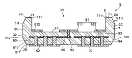
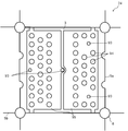
- FIG. 4 is a cross-sectional view of the element substrate of FIG. 3 taken along line X-X ′. It is the top view which looked at one Embodiment of the light-emitting device of this invention from the upper surface side.
- FIG. 6 is a cross-sectional view of the light emitting device of FIG. 5 taken along line Y-Y ′.
- connection board of the present invention is a connection board in which a plurality of unit element substrates partitioned by vertical and horizontal dividing grooves are formed on a mother substrate made of an inorganic insulating material, and each of the element substrates is mounted with a light emitting element in part.
- the entire light emitting element has a sealing region that is sealed with a sealing material, and a peripheral region in contact with the sealing region (that is, in contact with or close to the sealing region of the element substrate of each unit).
- the surface roughness Ra of the surface of the upper surface of the element substrate outside the sealing region is 0.15 ⁇ m or less, and the surface roughness Ra of the inner surface of the dividing groove is 0.15 to 0. It is characterized by being 5 ⁇ m.
- the surface roughness Ra of the peripheral region in contact with the sealing region is 0.15 ⁇ m or less, the penetration of the sealing material in the vicinity of the sealing region can be suppressed in each element substrate. Bleeding on the substrate can be suppressed. Further, by setting the surface roughness Ra of the inner surface of the divided groove to 0.15 to 0.5 ⁇ m, the division accuracy can be improved, and a connected substrate with less occurrence of burrs and chips on each substrate obtained after the division can be obtained.
- the surface roughness Ra is represented by 3 “Definition and display of defined arithmetic average roughness” of JIS: B0601 (1994), and Surfcom 1400D (model name, manufactured by Tokyo Seimitsu Co., Ltd.) Is a value measured by
- FIG. 1 is a plan view showing an example of an embodiment of a connection board of the present invention
- FIG. 2 is a cross-sectional view of the connection board 1 shown in FIG.
- a connecting substrate 1 has a substantially flat mother board 2 made of an inorganic insulating material.
- the mother board 2 in the central portion of the mother board 2, there are 9 columns in total, 3 columns (a column, b column, c column) and 3 rows (A row, B row, C row) horizontally.
- the element substrates 3 are arranged adjacent to each other as structural units.
- the “substantially flat plate” refers to what appears to be a flat plate at the visual level
- the term “substantially” refers to what appears to be at the visual level hereinafter.
- the boundary line between nine adjacent element substrates 3 in the structural unit and the boundary line between the mother substrate surplus portion 4 and the element substrate 3 are composed of a vertical division groove 5a and a horizontal division groove 5b.
- Divided grooves 5 are provided on one main surface 2A (hereinafter referred to as upper surface 2A) of mother substrate 2. Further, as shown in FIG. 2, the dividing groove 5 is also provided at a position corresponding to the dividing groove 5 on the upper surface 2 ⁇ / b> A on the lower surface 2 ⁇ / b> B that is the main surface opposite to the upper surface 2 ⁇ / b> A.
- the connecting substrate 1 is finally divided by means such as applying stress to the dividing grooves 5 to become nine independent element substrates 3.
- a total of 16 division holes 6 penetrating from the upper surface 2A side to the lower surface 2B side of the mother substrate 2 so as to cut out four corners of each element substrate 3 are provided. Is formed.
- Examples of the inorganic insulating material constituting the mother substrate 2 include an aluminum oxide sintered body (alumina ceramics), an aluminum nitride sintered body, a mullite sintered body, and a glass ceramic composition containing glass powder and ceramic powder.
- Examples thereof include LTCC (Low Temperature Co-fired Ceramics).
- LTCC Low Temperature Co-fired Ceramics
- LTCC is preferable from the viewpoints of high reflectivity, ease of production, easy processability, economy, and the like.
- a frame 7 is formed on the upper surface 2A of each element substrate 3 so as to surround the periphery of each unit element substrate.
- the frame body 7 is formed in a convex frame shape around the element substrate 3 of each unit, and the convex frame body 7 forms a circular shape inside the frame body 7.
- a cavity having a bottom as a part is formed, and a region in the cavity is a sealing region 22 into which a sealing material such as silicone resin is injected later and sealed.
- a circular bottom surface surrounded by the frame body 7 is an element mounting surface 21 on which a light emitting element is actually mounted.
- a peripheral region 8 is formed in contact with the sealing region 22 via the outer peripheral edge 711 of the cavity. That is, the peripheral region 8 is a peripheral region of the upper surface 71 of the frame body 7 on the side in contact with the upper peripheral edge of the side wall portion of the frame body 7 that forms the periphery of the sealing region 22. Indicates the above region.
- the surface roughness Ra of the peripheral region 8 is 0.15 ⁇ m or less. When the surface roughness Ra of the peripheral region 8 exceeds 0.15 ⁇ m, the silicone resin injected into the cavity is near the boundary between the peripheral region 8 and the sealing region 22 (that is, the outer peripheral edge 711). It becomes easy to penetrate into the peripheral region 8 due to the unevenness of the surface, and bleeding or the like is likely to occur on the upper surface 2A after sealing.
- the surface roughness Ra of the peripheral region 8 is more preferably 0.01 to 0.1 ⁇ m.
- the peripheral region 8 is the entire peripheral region 8 formed by the upper surface 71 of the frame body 7, but the peripheral region 8 is connected to the sealing region 22 on the upper surface 71 of the frame body 7. As long as it is circumscribed, it does not necessarily have to be the entire region of the upper surface 71 of the frame body 7, and may be a region formed with a predetermined distance from the outer peripheral edge 711 to the outside (dividing grooves 5 a, 5 b side).
- the peripheral region 8 is preferably a region having a distance of 100 ⁇ m outward from the outer peripheral edge 711 (that is, more than 0 to 100 ⁇ m outward from the outer peripheral edge 711).
- the surface roughness Ra of the groove inner surface 51 of the divided grooves 5 (5a, 5b) provided on the upper surface 2A and the lower surface 2B of the mother substrate 2 is 0.15 to 0.5 ⁇ m.
- the surface roughness of the groove inner surface 51 of the dividing groove 5 is less than 0.15, the division accuracy of the connection substrate 1 (that is, the connection substrate is divided along the division groove, and each element substrate is obtained with desired accuracy. And the burrs and chips are likely to occur in each element substrate obtained after the division.
- the surface roughness of the groove inner surface 51 of the dividing groove 5 exceeds 0.5 ⁇ m, the moldability as a substrate cannot be maintained sufficiently.
- the surface roughness Ra of the groove inner surface 51 of the divided groove 5 (5a, 5b) is more preferably 0.2 to 0.3 ⁇ m.
- the width of the opening 52 in which the dividing groove 5 opens in the upper surface 2A and the lower surface 2B of the mother substrate is preferably 1 to 30 ⁇ m.
- the width of the opening 52 is less than 1 ⁇ m, the division accuracy of the connection substrate 1 is lowered, and burrs and chips are easily generated on each element substrate 3 after division.
- the width of the opening 52 exceeds 30 ⁇ m, the abrasive particles used for the blasting process easily enter the divided grooves 5 in the wet blasting process described later. For this reason, the groove inner surface 51 of the dividing groove 5 is polished, and it is difficult to obtain a desired surface roughness Ra on the groove inner surface 51.
- the width of the opening 52 is more preferably 5 to 10 ⁇ m.
- the distance from the surface of the opening 52 of the dividing groove 5 (that is, the surface formed by the extended virtual surface of the upper surface 71 of the frame 7 in the opening 52) to the lower end 512 (that is, the depth of the dividing groove 5) is 100 to 400 ⁇ m is preferable. If the distance from the opening 52 to the lower end 512 is less than 100 ⁇ m, sufficient division accuracy cannot be obtained. On the other hand, if the distance from the opening 52 to the lower end 512 exceeds 400 ⁇ m, the moldability of the mother substrate is lowered.
- the distance from the opening 52 to the lower end 512 of the dividing groove 5 is more preferably 200 to 300 ⁇ m.
- the distance from the upper end 511 to the lower end 512 is more preferably 200 to 300 ⁇ m. This distance corresponds to the length of the inclined surface of the element substrate after division.
- the cross-sectional shape of the dividing groove 5 is preferably a triangular shape or an inverted triangular shape, but is not necessarily limited to such a shape, and is not necessarily limited to a trapezoidal shape, an inverted trapezoidal shape, a U shape, or an inverted U shape. It may be a letter shape or a rectangular shape.
- the dividing grooves 5 are provided on both main surfaces (2A, 2B) of the mother board 2, but are not necessarily provided on both main surfaces, and are provided only on the upper surface 2A or the lower surface 2B. You can also In addition, the depth of the dividing groove 5 and the length of the inclined surface of the dividing groove 5 may be substantially the same because the width of the opening 52 is sufficiently narrow with respect to the depth.
- connection substrate 1 of the present invention has been described with an example, but the configuration can be appropriately changed as long as it does not contradict the gist of the present invention.
- substrate 1 of this invention showed the structure which has the mother board
- substrate is provided on the mother board
- the connection substrate does not mean that the element substrates 3 are joined or bonded to each other, but is a substrate in which the element substrates 3 of each unit to be obtained are formed in a row. Means.
- the element substrate of the present invention is an element substrate in which a light emitting element is partially mounted on a substrate body made of an inorganic insulating material, and a sealing region in which the entire light emitting element is sealed with a sealing material is formed.
- the surface roughness Ra of the surface of the peripheral region in contact with the sealing region is 0.15 ⁇ m or less, and the inclination of the substrate body side surface descends from one main surface side to the other main surface side of the substrate body
- the surface roughness Ra of the surface is 0.15 to 0.5 ⁇ m.
- Such an element substrate is obtained, for example, by dividing the connecting substrate 1 shown in FIG. 1 along the dividing grooves 5.
- 3 is a plan view of the element substrate 3 of the present invention as viewed from the upper surface side
- FIG. 4 is a cross-sectional view of the element substrate of FIG. 3 cut along the line XX ′.
- the element substrate 3 has a substrate body 32 having a substantially square shape corresponding to each element substrate 3 of the connection substrate 1.
- the substrate body 32 is made of an inorganic insulating material.
- the frame body 7 is formed in a frame shape on the periphery of the substrate body 32.
- a cavity is formed by the frame 7, and a region in the cavity is a sealing region 22 to be sealed by a sealing material such as silicone resin later injected.
- a circular bottom surface surrounded by the frame body 7 is an element mounting surface 21 on which a light emitting element is actually mounted.
- a wiring conductor layer 91 that is electrically connected to the light emitting element is provided on the element mounting surface 21 of the substrate body 32.
- the wiring conductor layer 91 has a first electrode 911 and a second electrode 912.
- the first electrode 911 is one anode side or cathode side electrode (first electrode) disposed in the center of the element mounting surface 21.
- the second electrode 912 is a plurality of electrodes (second electrodes) disposed on the periphery of the element mounting surface 21 on the side opposite to the first electrode. In the second electrode 912, eight electrodes having the same number as that of the light-emitting element to be mounted are disposed on the circumference surrounding the first electrode 911 at substantially equal intervals.
- a region excluding such a portion where the wiring conductor layer 91 is formed from the element mounting surface 21 of the substrate body 32 is a light-emitting element mountable region T (hereinafter simply referred to as a mounting portion T).
- the number of second electrodes 912 in the wiring conductor layer 91 disposed on the element mounting surface 21 is eight, which is the same as the number of light emitting elements to be mounted. If there is an electrode or the like, the wiring conductor layer 91 can be formed as necessary. That is, the planar shape and arrangement position of the first electrode 911 constituting the wiring conductor layer 91 and the planar shape and number of the second electrodes 912 are not limited to those illustrated.
- the constituent material of the wiring conductor layer 91 is not particularly limited as long as it is the same as the wiring conductor layer used for a normal light emitting element substrate. Specifically, it will be described in the manufacturing method described later.
- the thickness of the wiring conductor layer 91 is preferably 5 to 15 ⁇ m.
- a pair of external electrode terminals 92 are provided on the lower surface 2B of the substrate body 32. These external electrode terminals 92 are electrically connected to the first electrode 911 and the second electrode 912 provided on the upper surface 2A side of the substrate body 32 through connection vias 93 formed in the substrate body 32 and the like, respectively. Connected.
- the shape and constituent materials of the external electrode terminal 92 and the connection via 93 can be used without particular limitation as long as they are the same as those used for a normal light emitting element substrate. Further, regarding the arrangement of the external electrode terminals 92 and the connection vias 93, the eight light emitting elements to be mounted are electrically connected in parallel via these, the first electrode 911 and the second electrode 912. It only has to be arranged. This will be specifically described in the section of the substrate manufacturing method described later.
- the thermal via 94 and the heat radiation layer 95 are embedded in the substrate body 32.
- the thermal via 94 is penetrated from the lower surface 2B of the substrate body 32 to the mounting portion T, the thermal resistance can be reduced, but the flatness of the mounting portion T is deteriorated, and the thermal contact between the mounted element and the mounting portion T is poor.
- the thermal via 94 is preferably columnar, for example, smaller than the mounting portion T of the light emitting element, and is preferably disposed from the lower surface 2B to the heat radiation layer 95 embedded therein.
- the thermal via 94 and the mounting portion T are arranged with a substrate material or the like, the flatness of the element mounting surface 21, particularly the mounting portion T can be improved, the thermal resistance is reduced, and the light emitting element Inclination when equipped with can also be suppressed.
- the shape and arrangement of the thermal via 94 and the heat dissipation layer 95 will be specifically described in the section of the substrate manufacturing method described later.
- a peripheral region 8 that is in contact with the sealing region 22 via an outer peripheral edge 711 is formed on the upper surface 71 of the frame body 7.
- the surface roughness Ra of the peripheral region 8 is 0.15 ⁇ m or less.
- the silicone resin injected into the cavity near the boundary (outer peripheral edge 711) between the peripheral region 8 and the sealing region 22 is formed on the surface of the substrate body 32. It becomes easy to penetrate into the peripheral region 8 due to the unevenness, and bleeding or the like is likely to occur on the peripheral region 8 after sealing.
- the peripheral region 8 is the entire peripheral region 8 formed by the upper surface 71 of the frame body 7, but the peripheral region 8 is connected to the sealing region 22 on the upper surface 71 of the frame body 7.
- the entire area of the upper surface 71 of the frame body 7 is not necessarily required, and may be an area formed on the outer peripheral edge side of the upper surface 2A with a predetermined distance outside the outer peripheral edge 711.
- the peripheral region 8 is preferably a region having a distance of more than 0 to 100 ⁇ m outward from the outer peripheral edge 711.
- the side surface 2C of the substrate body 32 is formed with an inclined surface 510 that descends from the upper surface 2A side to the lower surface 2B side of the frame body 7 of the substrate body 32 (see FIG. 4).
- the inclined surface 510 is formed with the side edge of the upper surface 2 ⁇ / b> A of the frame body 7 of the substrate body 32 as the upper end 511.
- the element substrate 3 is formed by dividing the connection substrate 1 of FIG. 1, and in this case, the inclined surface 510 is a surface formed by exposing the groove inner surface 51 of the divided groove 5.
- the lower end 512 of the inclined surface 510 corresponds to the lower end 512 of the groove inner surface 51 of the dividing groove 5.
- the inclined surface 510 that is inclined toward the upper surface 2A side is also formed on the lower surface 2B side of the side surface 2C (see FIG. 4).
- the inclined surface 510 may be formed only on the upper surface 2A side or the lower surface 2B side.
- the surface roughness Ra of the inclined surface 510 is 0.15 to 0.5 ⁇ m. If the surface roughness Ra of the inclined surface 510 is less than 0.15 ⁇ m, the presence of burrs and chips existing on the end face of the substrate body 32 is excessive, and the outer dimensions fluctuate due to the burrs. It becomes easy to produce the malfunction by, and the appearance is also inferior. On the other hand, if the surface roughness Ra of the inclined surface 510 exceeds 0.5 ⁇ m, the moldability as a substrate is not sufficient, and the presence of burrs on the substrate increases. The surface roughness Ra of the inclined surface 510 is more preferably 0.17 to 0.3 ⁇ m.
- the distance from the upper end 511 to the lower end 512 of the inclined surface 510 is preferably 100 to 400 ⁇ m. If the distance from the upper end 511 to the lower end 512 is less than 100 ⁇ m, the presence of burrs and chips on the substrate becomes excessive. On the other hand, when the distance from the upper end 511 to the lower end 512 exceeds 400 ⁇ m, the strength of the substrate body 32 and the frame body 7 is lowered.
- the element substrate 3 has a structure having the substrate body 32 in which the cavity is formed.
- the element substrate 3 of the present invention is not limited to such a mode, and for example, a flat substrate body.
- a structure having 32 may be used.
- FIG. 5 is a plan view of an embodiment of the light emitting device of the present invention as viewed from the upper surface side
- FIG. 6 is a cross-sectional view of the light emitting device of FIG. FIG. 5 shows a state where the resin sealing layer is removed.
- the light emitting device 10 of the present invention is mounted on the above-described element substrate 3 of the present invention and the mounting portion T of the element substrate 3, and the pair of electrodes are the first electrode 911 and the first electrode of the predetermined wiring conductor layer 91, respectively.
- a light emitting element 11 such as eight LED elements of a two-wire type, which is wire-bonded to two electrodes 912 and connected in parallel.
- all the eight light emitting elements 11 are rectangular parallelepiped light emitting elements whose bottom surfaces are squares of the same size, and are arranged on the eight mounting portions T of the element substrate 3 and bonded. It is fixed to the mounting portion T using a silicone die bond material (not shown) that is an agent.
- each light emitting element 11 is connected to the first electrode 911 located at the center of the element mounting surface 21 of the element substrate 3 by the bonding wire 12, and the other electrode is A bonding wire 12 is connected to the closest electrode of the eight second electrode 912 groups.
- the 16 bonding wires 12 connecting the 8 to 16 electrodes of the 8 light emitting elements 11 are arranged so as not to cross each other. Further, a sealing layer 13 made of mold resin is provided so as to cover these light emitting elements 11 and bonding wires 12. Thereby, the whole sealing region 22 is sealed.
- the arrangement of the light emitting element 11 in the light emitting device 10 of the present invention is an arrangement in which the bonding wires 12 do not intersect when at least the electrode of the light emitting element 11 is connected to the first electrode 911 and the second electrode 912 of the element substrate 3. There is no limitation to the arrangement shown in FIG.
- the upper surface 71 of the frame body 7 formed on the substrate body 32 is in contact with the upper peripheral edge of the inner side wall portion of the frame body 7 that forms the periphery of the sealing region 22.
- the element substrate in which the surface roughness Ra of the peripheral region 8 is 0.15 ⁇ m or less and the surface roughness Ra of the inclined surface 510 formed on the side surface 2C of the substrate body 32 is 0.15 to 0.5 ⁇ m. 3 is used, the substrate main body 32 is less cracked or chipped, the mounting accuracy of the light emitting element is excellent, and the penetration of the sealing material into the substrate main body 32 can be suppressed, and a good appearance can be obtained.
- connection board capable of obtaining an element substrate for mounting eight 2-wire type light emitting elements connected in parallel. To do.
- FIGS. 7 to 9 one region of the plurality of element substrates 3 formed on the green sheets 23 to 25 is shown in an enlarged manner.
- connection substrate and the unfired connection substrate are denoted by the same reference numeral 1
- first electrode and the first electrode conductor paste layer are denoted by the same reference numeral 911
- thermal via and thermal The via conductor paste layer is denoted by the same reference numeral 94, and the others are the same.
- the main body green sheet includes an upper layer green sheet for forming an upper layer, an inner layer green sheet for forming an inner layer, and a lower layer green sheet for forming a lower layer.
- a green sheet for a frame is also produced in order to form a frame.
- the green sheet for the main body is prepared by adding a binder and, if necessary, a plasticizer, a dispersant, a solvent, etc. to a glass ceramic composition containing glass powder and ceramic powder, and preparing a slurry by a doctor blade method or the like. It can be manufactured by molding into a sheet and drying. Moreover, the green sheet produced in this way is processed into a predetermined shape to obtain a green sheet for a frame.
- the glass powder for main body for producing the green sheet for main body preferably has a glass transition point (Tg) of 550 ° C. or higher and 700 ° C. or lower.
- Tg glass transition point
- degreasing may be difficult
- 700 ° C. the shrinkage start temperature becomes high and the dimensional accuracy may be lowered.
- the glass powder is preferably one in which crystals precipitate when fired at 800 ° C. or higher and 930 ° C. or lower. In the case where crystals do not precipitate, there is a possibility that sufficient mechanical strength cannot be obtained. Furthermore, the thing whose crystallization peak temperature (Tc) measured by DTA (differential thermal analysis) is 880 degrees C or less is preferable. When Tc exceeds 880 ° C., the dimensional accuracy may be reduced.
- SiO 2 is 57 to 65%
- B 2 O 3 is 13 to 18%
- CaO is 9 to 23%
- Al 2 O 3 is 3% in terms of mol% based on oxide.
- Those containing at least one selected from K 2 O and Na 2 O in a total of 0.5 to 6% are preferable.
- SiO 2 becomes a glass network former.
- the content of SiO 2 is preferably 58% or more, more preferably 59% or more, and particularly preferably 60% or more. Further, the content of SiO 2 is preferably 64% or less, more preferably 63% or less.
- B 2 O 3 is a glass network former. If the content of B 2 O 3 is less than 13%, there is a possibility that the glass melting temperature or Tg may be too high. On the other hand, when the content of B 2 O 3 exceeds 18%, it is difficult to obtain a stable glass, and the chemical durability may be lowered.
- the content of B 2 O 3 is preferably 14% or more, more preferably 15% or more. Further, the content of B 2 O 3 is preferably 17% or less, more preferably 16% or less.
- Al 2 O 3 is added to increase the stability, chemical durability, and strength of the glass. If the content of Al 2 O 3 is less than 3%, the glass may become unstable. On the other hand, when the content of Al 2 O 3 exceeds 8%, the glass melting temperature and Tg may be excessively high.
- the content of Al 2 O 3 is preferably 4% or more, more preferably 5% or more. Further, the content of Al 2 O 3 is preferably 7% or less, more preferably 6% or less.
- CaO is added to increase glass stability and crystal precipitation, and to lower the glass melting temperature and Tg.
- the content of CaO is less than 9%, the glass melting temperature may be excessively high.
- the content of CaO exceeds 23%, the glass may become unstable.
- the content of CaO is preferably 12% or more, more preferably 13% or more, and particularly preferably 14% or more. Further, the content of CaO is preferably 22% or less, more preferably 21% or less, and particularly preferably 20% or less.
- K 2 O and Na 2 O are added to lower Tg.
- the glass melting temperature and Tg may be excessively high.
- the total content of K 2 O and Na 2 O exceeds 6%, chemical durability, particularly acid resistance may be lowered, and electrical insulation may be lowered.
- the total content of K 2 O and Na 2 O is preferably 0.8% or more and 5% or less.
- the glass powder for main bodies is not necessarily limited to what consists only of the said component, Other components can be contained in the range with which various characteristics, such as Tg, are satisfy
- the glass powder for main body is obtained by producing glass by melting a glass raw material so as to have the glass composition as described above, and grinding the obtained glass by a dry grinding method or a wet grinding method.
- a dry grinding method or a wet grinding method it is preferable to use water or ethyl alcohol as a solvent.
- the pulverizer include a roll mill, a ball mill, and a jet mill.
- the 50% particle size (D 50 ) of the glass powder for main body is preferably 0.5 ⁇ m or more and 2 ⁇ m or less. If D 50 of the glass powder is less than 0.5 [mu] m, handling the glass powder is likely to agglomerate are not only difficult, uniform dispersion becomes difficult. On the other hand, if the D 50 of the glass powder exceeds 2 ⁇ m, there is a possibility that increase and insufficient sintering of the glass softening temperature is generated.
- the particle diameter may be adjusted by classification as necessary after pulverization, for example. In the present specification, the particle diameter is measured by a particle diameter measuring apparatus using a laser diffraction / scattering method.
- the ceramic powder those conventionally used for the production of LTCC substrates can be used.
- alumina powder, zirconia powder, or a mixture of alumina powder and zirconia powder can be suitably used.
- the high refractive index ceramic powder is a component for improving the reflectance of the LTCC substrate that is a sintered body, and examples thereof include titania powder, zirconia powder, and stabilized zirconia powder. While the refractive index of alumina is about 1.8, the refractive index of titania is about 2.7 and the refractive index of zirconia is about 2.2, which is higher than that of alumina. .
- the D 50 of these ceramic powders is preferably 0.05 ⁇ m or more and 5 ⁇ m or less.
- Such glass powder and ceramic powder are mixed and mixed so that, for example, the glass powder is 30% by mass or more and 50% by mass or less, and the ceramic powder is 50% by mass or more and 70% by mass or less.
- a composition is obtained.
- a slurry can be obtained by adding a binder and, if necessary, a plasticizer, a dispersant, a solvent, and the like to the glass ceramic composition.
- binder for example, polyvinyl butyral, acrylic resin or the like can be suitably used.
- plasticizer for example, dibutyl phthalate, dioctyl phthalate, butyl benzyl phthalate and the like can be used.
- solvent organic solvents such as toluene, xylene, 2-propanol and 2-butanol can be preferably used.
- the slurry thus obtained is formed into a sheet by a doctor blade method or the like and dried to produce three green sheets for the main body (upper layer green sheet, lower layer green sheet and inner layer green sheet). . Further, a green sheet manufactured in the same manner is processed into a predetermined shape to produce a frame green sheet.
- Conductive paste layer forming step Conductive paste layer for forming a wiring conductive layer, external electrode terminals, connection vias, thermal vias, heat dissipation layers, etc. on the surface and inside of the main body green sheet produced in the above step ( That is, an unsintered wiring conductor layer, unsintered external electrode terminals, unsintered connection vias, unsintered thermal vias, unsintered heat dissipation layers, and the like are formed. That is, as shown in FIG. 7, a circular first electrode conductive paste layer 911 is formed in the center of the element mounting surface 21 of each element substrate 3 in the upper layer green sheet 23.
- a ring-shaped connecting conductor paste layer 913 is formed so as to surround the first electrode conductor paste layer 911, and the eight second electrode conductor paste layers 912 are connected to the connecting conductor paste layer 913. It is formed at substantially equal intervals so as to extend inward from the inside. Further, a conductive paste layer 93 for connection via is formed through the upper green sheet 23 at a predetermined position of the central portion of the first electrode conductive paste layer 911 and the connecting conductive paste layer 913.
- a heat radiation layer conductor paste layer 95 is formed on the upper surface thereof, and a plurality of connection via conductor paste layers 93 are formed so as to penetrate the green sheet.
- a plurality of thermal via conductor paste layers 94 are formed.
- connection via conductor paste layers 93 and a plurality of thermal via conductor paste layers 94 are formed so as to penetrate the lower layer green sheet 25, and A conductor paste layer 92 for external electrode terminals is formed on the lower surface.
- the first electrode conductor paste layer 911 of the upper layer green sheet 23 is thermally connected to the heat dissipating layer conductor paste layer 95 by the connection via conductor paste layer 93.
- the external electrode terminal conductor paste layer 92 is thermally connected to the heat radiation layer conductor paste layer 95 by a thermal via conductor paste layer 94.
- the electrode conductor paste layer 911 is electrically connected to the heat dissipation layer conductor paste layer 95 by the connection via conductor paste layer 93, and the heat dissipation layer conductor paste layer 95 is connected via the connection via conductor paste layer 95.
- 93 is electrically connected to one of the external electrode terminal conductive paste layers 92.
- the other external electrode terminal conductor paste layer 92 is electrically connected to the electrode conductor paste layer 912 by a connection via conductor paste layer 93.
- Examples of the method for forming the conductive paste layer 92 include a method of applying or filling the conductive paste by screen printing. The thickness of these formed conductive paste layers is such that the first and second electrodes, connection wirings, connection vias, heat dissipation layers, thermal vias, and external electrode terminals finally obtained have a predetermined thickness. It is adjusted to become.
- a paste obtained by adding a vehicle such as ethyl cellulose to a metal powder mainly composed of copper, silver, gold or the like, and a solvent or the like as required can be used.
- a metal powder silver powder, metal powder composed of silver and platinum, and metal powder composed of silver and palladium are preferably used.
- step (C) Laminating step Green sheet 25 for lower layer with unfired conductor paste layer, green sheet 24 for inner layer with unfired conductor paste layer, and upper layer with unfired conductor paste layer obtained in step (B)
- the green sheet 23 is overlapped in this order to form an unfired main body member, and the frame green sheet is further stacked on the upper layer green sheet 23 and then integrated by thermocompression bonding.
- a green sheet molded body unfired mother substrate
- the dividing groove 5 formed on the unfired mother substrate is preferably formed so that the width of the opening 52 opened on the upper surface 2A and the lower surface 2B on the fired mother substrate 2 is 5 to 50 ⁇ m.
- (E) Firing step The unfired connecting substrate 1 obtained in the above step is degreased with a binder or the like as necessary, and then fired to sinter the glass ceramic composition or the like to obtain the connecting substrate 1.
- the surface roughness Ra of the region including at least the groove inner surface of the divided groove of the mother substrate after firing can be 0.15 to 0.5 ⁇ m.
- Degreasing is performed, for example, under the condition of holding at a temperature of 500 ° C. to 600 ° C. for 1 hour to 10 hours.
- the degreasing temperature is less than 500 ° C. or the degreasing time is less than 1 hour, the binder or the like may not be sufficiently removed.
- the degreasing temperature is about 600 ° C. and the degreasing time is about 10 hours, the binder and the like can be sufficiently removed, and if it exceeds this, productivity and the like may be lowered.
- the time can be appropriately adjusted in the temperature range of 800 ° C. to 930 ° C. in consideration of acquisition of a dense structure of the mother substrate 2, division accuracy, and productivity. Specifically, holding at a temperature of 850 ° C. or higher and 900 ° C. or lower for 20 minutes or longer and 60 minutes or shorter is preferable, and a temperature of 860 ° C. or higher and 880 ° C. or lower is particularly preferable.
- the firing temperature is less than 800 ° C., the mother substrate 2 may not be obtained as a dense structure.
- the firing temperature exceeds 930 ° C.
- the structure of the mother board 2 becomes too dense, the surface roughness Ra of the groove inner surface 51 of the dividing groove 5 becomes excessively low, and the dividing accuracy of the mother board 2 may be lowered. There is. In addition, productivity and the like may be reduced due to deformation of the mother board 2.
- a conductive paste containing a metal powder containing silver as a main component is used as the conductive paste, if the firing temperature exceeds 880 ° C., the predetermined shape may not be maintained due to excessive softening. .
- (F) Wet blasting process The upper surface 2A and the lower surface 2B of the mother substrate 2 in which the dividing grooves 5 are formed, the side wall portion inside the frame body 7, the element mounting surface 21, and the element mounting surface 21 are formed.
- the wiring conductor layer 91 is subjected to a wet blasting process in which a blast liquid obtained by mixing an abrasive with a liquid medium such as water is sprayed at a high pressure.
- a wet blasting process the convex portions of the fired surface forming a surface roughness of 0.15 to 0.5 ⁇ m are removed, and the surface of the mother substrate 2 is smoothed.
- the surface roughness Ra of the mother substrate 2 after the processing can be made 0.15 ⁇ m or less.
- a polishing material having a particle diameter that is 1 to 10 times the opening width of the opening 52 opened on the main surface (upper surface 2A, lower surface 2B) of the fired mother substrate 2. . It is preferable to use such an abrasive because the abrasive hardly penetrates into the grooves of the dividing grooves 5 and only the surface of the mother substrate 2 can be polished.
- the particle diameter of the abrasive is less than 1 times the opening width of the opening 52 of the divided groove 5
- the abrasive may enter the divided groove 5 during the blasting process, and the groove inner surface 51 may be polished. In this case, the surface roughness Ra becomes excessively low, and sufficient division accuracy cannot be obtained in the obtained connecting substrate 1.
- abrasive for example, ceramic powder such as alumina or zirconia can be used. In order to increase the efficiency of blasting, it is preferable to use crushed alumina powder.
- the 50% particle size (D 50 ) of the abrasive is preferably in the range of 25 to 150 ⁇ m. Is less than D 50 of the abrasive 25 [mu] m, abrasive enters the dividing groove 5, the surface roughness Ra is polished inner wall surface 51 becomes too low, divided accuracy may be degraded. In addition, the abrasive that enters the dividing groove 5 may become a foreign substance and hinder the mounting of the light emitting element.
- D 50 of the abrasive exceeds 150 [mu] m, in the peripheral region 8, there may not be efficiently blasted area near the outer peripheral edge 711 which is a boundary between the sealing region 22.
- the D 50 of the abrasive is preferably in the range of 80 to 100 ⁇ m. A more preferable D 50 is 90 ⁇ m.
- the mixing ratio of the abrasive and water as the liquid medium is preferably 20 to 60% by volume of the abrasive as a whole.
- the mixing ratio of the abrasive is less than 20% by volume, the efficiency of wet blasting is extremely low, and the surface of the mother substrate 2 cannot be sufficiently smoothed.
- the ratio of the abrasive exceeds 60% by volume, the viscosity of the blast liquid becomes too high, and the blasting efficiency is lowered.
- a specific example of the most preferable mixing ratio is a ratio of 40% by volume of the abrasive and 60% by volume of water.
- the pressure for injecting the blast liquid mixed at such a ratio is preferably 1.2 to 1.8 kg / cm 2 when, for example, the injection port of the boron carbide nozzle has a diameter of 8 mm. If the spray pressure of the blast liquid is less than 1.2 kg / cm 2 , it becomes difficult to sufficiently smooth the surface roughness Ra of the mother substrate 2 to 0.15 ⁇ m or less, and the effect of preventing the penetration of the sealing material is sufficient. May not be granted. If the spray pressure of the blast liquid exceeds 1.8 kg / cm 2 , alumina powder as a blast material adheres to the upper surface 2A of the mother substrate 2 and the effect of smoothing the surface of the mother substrate 2 becomes small.
- the diameter of the nozzle of the boron carbide nozzle can be 5 to 10 mm. If the thickness is 5 mm or less, the flow velocity becomes too strong, and a large amount of glass and ceramic powder on the mother substrate 2 is removed to reduce the strength, or alumina powder adheres, and the surface of the mother substrate 2 is smoothed. Get smaller. When the thickness is 10 mm or more, sufficient smoothing such that the surface roughness Ra of the mother substrate is 0.15 ⁇ m or less cannot be performed.
- a blast liquid is injected from an ejection port having a diameter of 8 mm of a boron carbide nozzle disposed about 5 cm above the conveying surface toward the upper surface 2A of the mother substrate 2 continuously conveyed by the belt conveyor. Can be taken.
- the conveying speed of the conveyor is preferably 1 to 1.5 m / min. When the conveyance speed is less than 1 m / min, alumina powder as a blast material adheres to the upper surface 2A and the like, and the effect of smoothing the surface is small. When the conveyance speed exceeds 1.5 m / min, the effect of blasting is small, and smoothing sufficient to prevent the penetration of the sealing material in the peripheral region 8 cannot be performed.
- the surface of the mother substrate 2 subjected to the blasting treatment of the connecting substrate 1 obtained as described above has a surface roughness Ra as low as 0.15 ⁇ m or less and a dense structure, and prevents the penetration of the sealing material.
- the groove inner surface 51 of the dividing groove 5 is not subjected to the blasting process, so that an appropriate surface roughness can be maintained and a connection substrate with good division accuracy can be obtained.
- wet blasting is performed on the entire surface of the mother substrate 2 after firing.
- the wet blasting may be performed at least on the upper surface 2A of the mother substrate 2, and is not necessarily performed on the mother substrate 2. It is not necessary to treat the entire surface.
- the case where the glass ceramic composition (LTCC) is used as the mother substrate has been described.
- the ceramic sintered body constituting the mother substrate 2 as described above, the aluminum oxide sintered body is used.
- an aluminum nitride sintered body, a mullite sintered body, or the like may be used.
- add binder, plasticizer, dispersant, solvent, etc. as necessary to the raw material composition of the ceramic sintered body to be used, as with LTCC.
- a firing temperature suitable for the ceramic sintered body to be used for example, aluminum oxide A sintered body obtained by firing at 1400 to 1700 ° C. for the sintered material and 1700 to 1950 ° C. for the aluminum nitride sintered body is used.
- a raw material of the ceramic sintered body containing the above aluminum as a main component for example, a compound such as aluminum oxide, aluminum hydroxide, aluminum halide, aluminum sulfate, aluminum nitrate, aluminum sulfide, aluminum nitride, feldspar ( NaAlSi 3 O 8 ), alum (KAl 3 (OH) 6 (SO 4 ) 2 ), boehmite (AlO (OH)), corundum (Al 2 O 3 ), kaolinite (Al 2 Si 2 O 5 (OH) 4 ), Mullite (Al 6 Si 2 O 13 ), sericite (KAl 2 (AlSi 3 O 10 ) (OH) 2 ) and other minerals containing the compound, or composites made from the compound as raw materials.
- a compound such as aluminum oxide, aluminum hydroxide, aluminum halide, aluminum sulfate, aluminum nitrate, aluminum sulfide, aluminum nitride, feldspar ( NaAlS
- the plasticizer, dispersant, solvent, and the like, which are binders and optional components for preparing the slurry, can be the same as those of the LTCC.
- it can carry out similarly to the said LTCC except the said baking conditions.
- connection substrate 1 The manufacturing method of the connection substrate 1 has been described above, but the frame green sheet need not be a single green sheet, and may be a laminate of a plurality of green sheets. Further, the number of main body green sheets excluding the frame green sheet is not necessarily three, and may be two or four or more. Furthermore, the order of forming each part can be changed as appropriate as long as the connection substrate 1 can be manufactured.
- connection substrate shown in FIGS. 1 and 2 was manufactured by the method described below.
- main body green sheets (upper layer green sheet, lower layer green sheet, and inner layer green sheet) for preparing the mother substrate 2 of the connection substrate 1 were prepared.
- SiO 2 is 60.4%
- B 2 O 3 is 15.6%
- Al 2 O 3 is 6%
- CaO is 15%
- K 2 O is 1%
- Na 2 O is blended glass raw materials to be 2% of the glass composition, mixing, after the raw material mixture was melted for 60 minutes at placed in 1600 ° C. in a platinum crucible and molten glass Was poured out and cooled.
- This glass was pulverized with an alumina ball mill for 40 hours to produce a glass powder for a main body.
- ethyl alcohol was used as a solvent for pulverization.
- the glass powder, alumina filler (product name: AL-45H, manufactured by Showa Denko KK), and zirconia filler (product name: HSY-3F-J, manufactured by Daiichi Rare Element Chemical Industry Co., Ltd.) are shown in Table 1, respectively.
- the glass ceramic compositions for substrate bodies of Examples 1 and 2 and Comparative Examples 1 and 2 were produced by blending in the proportions shown and mixing. In addition, the composition ratio of each component in Table 1 is expressed in mass%.
- this glass ceramic composition 15 g of an organic solvent (mixed with toluene, xylene, 2-propanol, 2-butanol in a mass ratio of 4: 2: 2: 1), a plasticizer (di-2-ethylhexyl phthalate) 2.5 g of polyvinyl butyral (trade name: PVK # 3000K, manufactured by Denka Co., Ltd.) as a binder, 5 g, and 0.5 g of a dispersant (trade name: BYK180, manufactured by Big Chemie) were blended and mixed to prepare a slurry. .
- an organic solvent mixed with toluene, xylene, 2-propanol, 2-butanol in a mass ratio of 4: 2: 2: 1
- a plasticizer di-2-ethylhexyl phthalate
- polyvinyl butyral trade name: PVK # 3000K, manufactured by Denka Co., Ltd.
- a dispersant trade name
- This slurry is applied onto a PET film by a doctor blade method and dried to produce a green sheet.
- the green sheet is laminated, is approximately flat, has a size after baking of 170 mm ⁇ 170 mm, and a thickness of 0.00.
- a green sheet for a main body of 5 mm was produced.
- a green sheet manufactured in the same manner as the green sheet for the main body is laminated to produce a substrate green sheet for a frame having a size of 170 mm ⁇ 170 mm and a thickness of 0.5 mm after firing. did.
- the central portion of nine element substrates 3 (5 mm ⁇ 5 mm in each region) was cut into a circle having a diameter of 4.4 mm using a green sheet punching machine. Further, at the 16 intersections of the boundary line 5 between the element substrates 3 and the boundary line 5 between the element substrate 3 and the mother board surplus part 4, a circular through-hole having a diameter of 0.6 mm centering on the intersection point is formed. To form divided holes 6.
- conductive metal powder (silver powder: manufactured by Daiken Chemical Industry Co., Ltd., trade name: S550) and ethyl cellulose as a vehicle are blended at a mass ratio of 85:15 so that the solid content is 85 mass%.
- conductive metal powder silver powder: manufactured by Daiken Chemical Industry Co., Ltd., trade name: S550
- ethyl cellulose as a vehicle are blended at a mass ratio of 85:15 so that the solid content is 85 mass%.
- the mixture was kneaded in a porcelain mortar for 1 hour and further dispersed three times with a three roll to produce a conductor paste.
- the conductor paste is screen-printed in the pattern shown in FIG. 7 on the upper surface of the upper layer green sheet 23 of the main body green sheet, and each conductor paste layer for the first electrode, the second electrode, and the connection is used. 911, 912, and 913 are formed, a through hole having a diameter of 0.15 mm is formed in a portion corresponding to the connection via using a hole puncher, and a conductive paste is filled by a screen printing method. Layer 93 was formed.
- the conductor paste is screen-printed with the pattern shown in FIG. 8 to form the conductor paste layer 95 for the heat dissipation layer, and a hole puncher is formed in a portion corresponding to the thermal via and the connection via.
- a through-hole having a diameter of 0.2 mm and a diameter of 0.15 mm was formed using, and a conductor paste was filled by a screen printing method to form a thermal via conductor paste layer 94 and a connection via conductor paste layer 93.
- a conductor paste is screen-printed on the lower surface of the lower layer green sheet 25 in the pattern shown in FIG. 9 to form a conductor paste layer 92 for external electrode terminals, and holes are formed in portions corresponding to thermal vias and connection vias. Through holes having a diameter of 0.2 mm and a diameter of 0.15 mm were formed using a machine, and a conductor paste was filled by screen printing to form a thermal via conductor paste layer 94 and a connection via conductor paste layer 93.
- the upper layer green sheet 23 with the conductor paste layer, the inner layer green sheet 24 with the conductor paste layer, and the lower layer green sheet 25 thus prepared are laminated in a predetermined order. After laminating a green sheet for a frame, it was integrated by heating and pressing. In this way, a green sheet molded body serving as a mother substrate was obtained. Next, on each of the front and back surfaces of the green sheet molded body, four divided grooves 5 (5a, 5b) having a depth of 300 ⁇ m are formed vertically and horizontally using a ceramic green sheet laminate cutting machine (G-cut 6 manufactured by UHT). And the unbaking connection board
- G-cut 6 manufactured by UHT ceramic green sheet laminate cutting machine
- the dividing groove 5 was formed so that the element substrate region 3 partitioned on the unfired connecting substrate 1 was 5.7 ⁇ 5.7 mm in each region.
- the division grooves 5 were formed so that the width of the opening 52 was 5 ⁇ m and the inclined surface after division was 350 ⁇ m in the dimension after sintering.
- the obtained green sheet molded body to be a mother substrate was degreased by holding at 550 ° C. for 5 hours.
- the substrate was held at 870 ° C. for 30 minutes and baked to produce a connection substrate 1.
- the surface roughness Ra of the upper surface 2A was measured with Surfcom 1400D (manufactured by Tokyo Seimitsu Co., Ltd.). The measurement results are shown in Table 1.
- the wet blast treatment was performed on the upper surface 2A of the connection substrate 1 of Examples 1 and 2 and Comparative Example 1 under the following conditions.
- the mixing ratio of the abrasive (blast powder) and the liquid medium (water) in the blast liquid was such that the abrasive was 40% by volume of the entire blast liquid. Furthermore, the injection pressure for injecting the blast liquid mixed at such a ratio is 1.5 kg / cm 2, and it is 5 cm above the transfer surface toward the upper surface 2A of the mother board while being continuously transferred by the belt conveyor. Blasting of the upper surface 2A was performed by injecting blast liquid from an injection port having a diameter of 8 mm of the boron carbide nozzle arranged. The conveyor speed of the belt conveyor was 1.2 m / min. Here, the blasting, D 50 was used 80 ⁇ m abrasive.
- the surface roughness Ra of the upper surface 2A of the mother substrate 2 in the connection substrate 1 of Examples 1 and 2 and Comparative Example 1 after blasting treatment and the connection substrate 1 of Comparative Example 2 where blasting treatment is not performed is as above. Measurements were made in the same way and position. The measurement results are shown in Table 1.
- connection substrates 1 of Examples 1 and 2 and Comparative Examples 1 and 2 are divided along the division grooves 5a and 5b, and the surface roughness Ra of the inclined surface 510 of each element substrate 3 obtained is obtained.
- the measurement was performed in the same manner as described above. Further, in Examples 1 and 2 and Comparative Examples 1 and 2, the number of burrs and chips generated on the surface of the obtained element substrate 3 was measured to evaluate the division property. The measurement results are shown in Table 1.
- the evaluation of the splitting property (that is, dividing the connecting substrate along the dividing groove, and the division surface of the obtained element substrate, the degree of quality of the divided portion) is to observe the surface of the element substrate with an optical microscope, A sample having no burr of 100 ⁇ m or more and no chipping was indicated by “ ⁇ ”, and a sample having burr and chipping of 100 ⁇ m or more by “x”.
- the evaluation results are shown in Table 1.
- a sealing agent manufactured by Shin-Etsu Chemical Co., Ltd., trade name: SCR-1016A
- SCR-1016A a sealing agent
- ⁇ a sample in which no seepage was observed at 100 ⁇ m or more on the outside
- X a sample that was exuded on the outer side from the outer peripheral edge 711 of the sealing region 22 by 100 ⁇ m or more
- connection substrate 1 of Example 1 the surface roughness Ra of the upper surface 2A after blasting is 0.15 ⁇ m or less, and the surface of the inclined surface 510 corresponding to the groove inner surface 51 Since the roughness Ra is 0.15 to 0.5 ⁇ m, the penetration prevention property of the sealing material is excellent as “ ⁇ ”, and there is no occurrence of burrs or chips on the substrate after division. It was confirmed that a good splitting property could be obtained.
- the connection substrate 1 of Comparative Example 1 although the penetration preventing property of the sealing material is excellent as “ ⁇ ”, the separation accuracy is inferior, and burrs and chips are generated on the element substrate obtained after the division. Admitted.
- connection substrate 1 of Comparative Example 2 although there is no generation of burrs or chips on the substrate after the division and good division properties can be obtained, the value of the surface roughness Ra of the upper surface 2A exceeds 0.15 ⁇ m. In the vicinity of the outer peripheral edge 711, bleeding was recognized, and the penetration preventing property of the sealing material was poor.
- the light-emitting device using the element substrate of the present invention can be suitably used as a backlight for mobile phones, liquid crystal TVs, liquid crystal displays, etc., illumination for automobiles or decoration, and other light sources.
Landscapes
- Led Device Packages (AREA)
Abstract
分割精度に優れ、分割後の各素子基板のバリや欠けの発生が低減されるとともに、搭載面上での封止材の浸透を抑制できる連結基板を提供する。 無機絶縁材料からなる母基板2に、縦横の分割溝5によって区画された複数の素子基板3が形成された連結基板1で、各素子基板3は、一部に発光素子が搭載され、当該発光素子の全体が封止材で封止される封止領域8を有しており、封止領域8と接する周縁領域の表面粗さRaが0.15μm以下であり、分割溝5の溝内面51の表面粗さRaが0.15~0.5μmの連結基板1。
Description
本発明は、発光素子用連結基板(以下、連結基板と言う)およびその製造方法に係り、より詳細には、各々が電子部品を搭載するための素子搭載用基板(以下、素子基板と言う)を一つの構成単位として、複数個連結して配列形成された連結基板に関する。
また、本発明は、この連結基板を分割して得られる素子基板及びこれを用いた発光装置に関する。
また、本発明は、この連結基板を分割して得られる素子基板及びこれを用いた発光装置に関する。
近年、発光ダイオード(LED)素子の高輝度、白色化に伴い、携帯電話や液晶TV、液晶ディスプレイのバックライト等としてLED素子を用いた発光装置が使用されている。
LED素子等の発光素子を用いた発光装置は、従来、発光素子と、この発光素子の各電極に電気的に接続された一対のリードとを樹脂基板上に搭載し、またはこれらを樹脂基板の凹部に収容して構成されている。
例えば特許文献1では、樹脂ステムの凹部底面に各リードが配置されており、この凹部にシリコーン樹脂からなる光透過性部材が充填されて構成された発光装置が開示されている。
例えば特許文献1では、樹脂ステムの凹部底面に各リードが配置されており、この凹部にシリコーン樹脂からなる光透過性部材が充填されて構成された発光装置が開示されている。
近年、LED素子の高輝度化に伴って発熱量が増加しているため、LED素子等の発光素子を搭載するための基板として、上記の樹脂基板に代わり、耐熱性が高くかつ発光素子から発生する熱を速やかに放散して、十分な発光輝度が得られるものが求められている。
樹脂基板に代わる発光素子搭載用基板として、従来より、例えばアルミナ基板が用いられている。また、アルミナ基板のようなセラミックス基板に比べて反射率の高い発光素子搭載用基板として、低温同時焼成セラミックス基板(以下、LTCC基板という。)が使用されている。LTCC基板は、アルミナ粉末のようなセラミックス粉末とガラスとの焼結体からなり、ガラスとセラミックスとの屈折率差が大きく、光の入射方向に面する両者の界面の占める割合が多く、かつセラミックス粉末の粒径(厚み)が使用波長より大きいことから、高い反射率が得られる。そのため、発光素子からの光を効率よく利用できるため発熱量を低減できる。また、光源による劣化の少ない無機酸化物からなるため、長期間に亘って色調が安定する。
しかしながら、上記のセラミックス基板やLTCC基板等の無機材料基板において、基板表面に凹凸面が多いと、この表面をシリコーン樹脂等の封止材で封止したときに、封止部と非封止部との境界域において、凹凸面に封止材が染み込み、基板の外観が損なわれたり、発光時の発光エリアが乱れたりする。このため、基板本体の表面粗さを低減し、より緻密化することが求められている。
基板や金属導体表面の平滑化に関しては、例えば、基板等の表面を研磨剤でブラスト処理する。例えば特許文献2には、メッキ工程の前にLTCC基板の表面に対してウェットブラスト処理を施し、導体層の表面に浮き出したガラスを除去して表面を平滑化する方法が提案されている(例えば、特許文献2参照。)。また、特許文献3には、絶縁基板およびこれと一体化された外部リード端子表面を、サンドブラスト処理により研磨洗浄して表面を平滑化し、メッキ金属層の付着性を向上させる方法が開示されている。また、特許文献4には、金メッキ層との密着性を向上させることを目的として、無電解ニッケル層の表面にブラスト処理を施し、中心線平均粗さRaを所定の範囲に調整した配線基板が開示されている。
ところで、このような発光装置では、近年小型化の要求が高まっており、素子基板の基板サイズの小型化が進んでいる。小型の基板を作製する場合には、取扱い性を向上させるために、複数の基板が集合した連結配線基板に分割溝を設け、めっき処理や素子の実装等を行った後に個片に分割する。
連結配線基板は、例えば図1で示すように、広面積の母基板2の中央部に、素子基板となる素子基板領域3を縦横に複数個配列形成し、各素子基板領域3を区分する分割溝5を縦横に形成した。この分割溝5に沿って母基板2を分割して、複数の素子基板を効率的に製造できる。
しかしながら、上記の連結基板を分割溝5に沿って分割すると、分割後の素子基板3の表面に、分割溝5近傍の位置を中心として、バリや欠けが発生する。
特に、上記のように、基板の表面粗さRaを低減し、緻密化した場合には、個片分割性が低下し、バリや欠けが発生し易くなる。素子基板3にバリや欠けが存在すると、この素子基板3に電子部品を搭載する際、実装位置の精度が低下するおそれがある。
特に、上記のように、基板の表面粗さRaを低減し、緻密化した場合には、個片分割性が低下し、バリや欠けが発生し易くなる。素子基板3にバリや欠けが存在すると、この素子基板3に電子部品を搭載する際、実装位置の精度が低下するおそれがある。
本発明は、上記課題を解決するためになされたもので、分割精度に優れ、分割後の各素子基板のバリや欠けの発生を低減でき、また基板への封止材の浸透を抑制できる連結基板の提供を目的とする。また、本発明は、基板本体の割れや欠けが少なく、発光素子の搭載精度に優れるとともに、封止材の浸透を抑制でき、良好な外観を得られる素子基板の提供を目的とする。さらに本発明は、上記素子基板を用いた発光装置の提供を目的とする。
なお、本明細書で「浸透」とは、基板上に塗布された封止材が、基板上を広がり伸びることを意味している。
なお、本明細書で「浸透」とは、基板上に塗布された封止材が、基板上を広がり伸びることを意味している。
本発明の連結基板は、無機絶縁材料からなる母基板に、縦横の分割溝によって区画された複数単位の素子基板が形成された連結基板で、前記各素子基板は、一部に発光素子が搭載され、当該発光素子の全体が封止材で封止される封止領域を有しており、前記封止領域と接する周縁領域の表面粗さRaが0.15μm以下であり、前記分割溝の溝内面の表面粗さRaが0.15~0.5μmを特徴とする。
また、前記母基板に形成された複数単位の素子基板のそれぞれの上面の周囲には、額縁状の枠体が前記封止領域と接するように形成されており、前記額縁状の枠体の上面の少なくとも前記封止領域側の周縁領域の表面の表面粗さRaを0.15μm以下とし、前記分割溝の溝内面の表面粗さRaを0.15~0.5μmとするのが好ましい。また、前記封止領域と接する周縁領域は、前記封止領域の外周縁から外側に0超~100μmの距離を有する周縁領域が好ましい。また、前記分割溝が前記母基板の主面に対して開口する開口部の幅は1~30μmが好ましい。また、前記母基板の少なくとも分割溝を含む領域の表面は、ウェットブラストによるブラスト処理が施されたものが好ましい。また、前記母基板は、ガラス粉末とセラミックスフィラーとを含むガラスセラミックス組成物の焼結体からなる低温焼成セラミックが好ましい。
また、前記母基板に形成された複数単位の素子基板のそれぞれの上面の周囲には、額縁状の枠体が前記封止領域と接するように形成されており、前記額縁状の枠体の上面の少なくとも前記封止領域側の周縁領域の表面の表面粗さRaを0.15μm以下とし、前記分割溝の溝内面の表面粗さRaを0.15~0.5μmとするのが好ましい。また、前記封止領域と接する周縁領域は、前記封止領域の外周縁から外側に0超~100μmの距離を有する周縁領域が好ましい。また、前記分割溝が前記母基板の主面に対して開口する開口部の幅は1~30μmが好ましい。また、前記母基板の少なくとも分割溝を含む領域の表面は、ウェットブラストによるブラスト処理が施されたものが好ましい。また、前記母基板は、ガラス粉末とセラミックスフィラーとを含むガラスセラミックス組成物の焼結体からなる低温焼成セラミックが好ましい。
本発明の素子基板は、無機絶縁材料からなる基板本体に、一部に発光素子が搭載され、当該発光素子の全体が封止材で封止される封止領域が形成された素子基板で、前記封止領域と接する周縁領域の表面粗さRaが0.15μm以下であり、前記基板本体側面のうち該基板本体の一の主面側から他方の主面側に向けて下降する傾斜面の表面粗さRaが0.15~0.5μmを特徴とする。
また、前記素子基板の上面の周囲には、額縁状の枠体が前記封止領域と接するように形成されており、前記額縁状の枠体の上面の少なくとも前記封止領域側の周縁領域の表面の表面粗さRaを0.15μm以下とし、前記分割溝の溝内面の表面粗さRaを0.15~0.5μmとするのが好ましい。
また、前記封止領域と接する周縁領域は、前記封止領域の外周縁から外側に0超~100μmの距離を有する領域が好ましい。また、前記傾斜面の上端から下端までの距離が100~400μmが好ましい。また、本発明の素子基板は、上記した本発明の連結基板を分割溝に沿って分割して得たものが好ましい。
また、前記素子基板の上面の周囲には、額縁状の枠体が前記封止領域と接するように形成されており、前記額縁状の枠体の上面の少なくとも前記封止領域側の周縁領域の表面の表面粗さRaを0.15μm以下とし、前記分割溝の溝内面の表面粗さRaを0.15~0.5μmとするのが好ましい。
また、前記封止領域と接する周縁領域は、前記封止領域の外周縁から外側に0超~100μmの距離を有する領域が好ましい。また、前記傾斜面の上端から下端までの距離が100~400μmが好ましい。また、本発明の素子基板は、上記した本発明の連結基板を分割溝に沿って分割して得たものが好ましい。
本発明の発光装置は上記した本発明の素子基板と、この素子基板の前記素子搭載領域に搭載される発光素子と、を有することを特徴とする。
本発明の連結基板の製造方法は、未焼成母基板の主面上に分割溝を形成する工程と、前記分割溝を形成した未焼成母基板を焼成して、少なくとも分割溝の溝内面の領域を含む表面の表面粗さRaが0.15~0.5μmである母基板を形成する工程と、焼成後の前記母基板の表面にウェットブラスト処理を施して、前記母基板表面のうち少なくとも一の主面の表面粗さRaを0.15μm以下とする工程と、を有することを特徴とする。
また、前記未焼成母基板の焼成温度は800℃~930℃であり、焼成時間は20~60分が好ましい。また、前記ウェットブラスト処理は、焼成後の前記母基板の主面上の前記分割溝の開口部の幅の1~10倍の粒子径を有する研磨材の使用が好ましい。また、前記ウェットブラスト処理に使用される研磨材は、粒子径が25~150μmのセラミックス粉末であり、媒体は水が好ましい。また、前記研磨材の混合比率は、前記研磨材と前記水との全量に対して20~60体積%が好ましい。また、前記ウェットブラスト処理において、前記研磨材と前記水とからなるブラスト液の噴射圧力は、1.2~1.8kg/cm2が好ましい。
上記した数値範囲を示す「~」とは、特段の定めがない限り、その前後に記載された数値を下限値及び上限値として含む意味で使用され、特段の定めがない限り、以下本明細書において「~」は、同様の意味をもって使用される。
また、前記未焼成母基板の焼成温度は800℃~930℃であり、焼成時間は20~60分が好ましい。また、前記ウェットブラスト処理は、焼成後の前記母基板の主面上の前記分割溝の開口部の幅の1~10倍の粒子径を有する研磨材の使用が好ましい。また、前記ウェットブラスト処理に使用される研磨材は、粒子径が25~150μmのセラミックス粉末であり、媒体は水が好ましい。また、前記研磨材の混合比率は、前記研磨材と前記水との全量に対して20~60体積%が好ましい。また、前記ウェットブラスト処理において、前記研磨材と前記水とからなるブラスト液の噴射圧力は、1.2~1.8kg/cm2が好ましい。
上記した数値範囲を示す「~」とは、特段の定めがない限り、その前後に記載された数値を下限値及び上限値として含む意味で使用され、特段の定めがない限り、以下本明細書において「~」は、同様の意味をもって使用される。
本発明によれば、封止領域と接する周縁領域の表面粗さRaを0.15μm以下とするとともに、分割溝の溝内面の表面粗さRaを0.15~0.5μmとして、基板への封止材の浸透を抑制できるとともに、分割精度に優れ、分割時のバリや欠けの発生が低減された連結基板とすることができる。
また、本発明によれば、基板本体の割れや欠けが少なく、また封止材の浸透を抑制できる素子基板とすることができる。さらに本発明によれば、発光素子の実装精度が高く、また封止部と外接する周縁領域のにじみ等の発生が抑制された発光装置とすることができる。
また、本発明によれば、基板本体の割れや欠けが少なく、また封止材の浸透を抑制できる素子基板とすることができる。さらに本発明によれば、発光素子の実装精度が高く、また封止部と外接する周縁領域のにじみ等の発生が抑制された発光装置とすることができる。
以下、本発明の実施形態について詳細に説明する。
本発明の連結基板は、無機絶縁材料からなる母基板に、縦横の分割溝によって区画された複数単位の素子基板が形成された連結基板で、前記各素子基板は、一部に発光素子が搭載され、当該発光素子の全体が封止材で封止される封止領域を有しており、前記封止領域と接する周縁領域(すなわち、各単位の素子基板の封止領域に接する、あるいは近接する、封止領域の外側の素子基板の上面の周縁の領域)の表面の表面粗さRaが0.15μm以下であり、前記分割溝の溝内面の表面粗さRaが0.15~0.5μmであることを特徴とする。
本発明によれば、封止領域と接する周縁領域の表面粗さRaを0.15μm以下として、各素子基板において、封止領域近傍域での封止材の浸透を抑制できるため、封止後における基板上のにじみを抑制できる。また、分割溝の溝内面の表面粗さRaを0.15~0.5μmとして、分割精度を向上でき、分割後に得られる各基板上でのバリや欠けの発生が少ない連結基板とできる。
なお、本明細書において、表面粗さRaは、JIS:B0601(1994年)の3「定義された算術平均粗さの定義及び表示」によって表され、サーフコム1400D(機種名、東京精密社製)により測定された値である。
図1は本発明の連結基板の実施形態の一例を示す平面図であり、図2は、図1で示す連結基板1のA-A線断面図である。
図1において、連結基板1は、無機絶縁材料からなり略平板状の母基板2を有している。
図1に示した例では、母基板2の中央部には、縦に3列(a列、b列、c列)、横に3行(A行、B行、C行)、合計9個の素子基板3が構成単位として互いに隣接して配列されている。9個の素子基板3の外側には、これを囲むようにして母基板余剰部4が存在している。
ここで略平板とは目視レベルで平板と見えるものであり、以後、略とは目視レベルでそのように見えるものを指す。
図1において、連結基板1は、無機絶縁材料からなり略平板状の母基板2を有している。
図1に示した例では、母基板2の中央部には、縦に3列(a列、b列、c列)、横に3行(A行、B行、C行)、合計9個の素子基板3が構成単位として互いに隣接して配列されている。9個の素子基板3の外側には、これを囲むようにして母基板余剰部4が存在している。
ここで略平板とは目視レベルで平板と見えるものであり、以後、略とは目視レベルでそのように見えるものを指す。
構成単位の9個の隣接し合う素子基板3の境界線、および母基板余剰部4と素子基板3との境界線には、縦方向の分割溝5aと、横方向の分割溝5bとからなる分割溝5が、母基板2の一方の主面2A(以下、上面2Aと示す。)に設けられている。また、図2に示すように、上面2Aと反対側の主面である下面2Bにも、上面2Aの分割溝5に対応する位置に、分割溝5が設けられている。
連結基板1は、最終的に、分割溝5に応力を負荷する等の手段により分割されて、独立した9個の素子基板3となる。また、この分割における欠け等の不具合発生を防止するために、各素子基板3の4隅を切り欠くように、母基板2の上面2A側から下面2B側まで貫通する分割孔6が合計16個形成されている。
連結基板1は、最終的に、分割溝5に応力を負荷する等の手段により分割されて、独立した9個の素子基板3となる。また、この分割における欠け等の不具合発生を防止するために、各素子基板3の4隅を切り欠くように、母基板2の上面2A側から下面2B側まで貫通する分割孔6が合計16個形成されている。
母基板2を構成する無機絶縁材料としては、酸化アルミニウム質焼結体(アルミナセラミックス)や窒化アルミニウム質焼結体、ムライト質焼結体、ガラス粉末とセラミックス粉末とを含むガラスセラミックス組成物の焼結体(LTCC:Low Temperature Co-fired Ceramics)等が挙げられる。本発明においては、高反射性、製造の容易性、易加工性、経済性等の観点から、LTCCが好ましい。
各素子基板3の上面2Aには、それぞれの単位の素子基板の周囲を囲むように枠体7が形成されている。この枠体7は、各単位の素子基板3の周囲に凸状の額縁状に形成されており、この凸状となった枠体7により、この枠体7に囲まれた内側に、円形状部分を底面とするキャビティが形成されており、このキャビティ内の領域が、後にシリコーン樹脂等の封止材が注入されて封止される封止領域22とされている。
枠体7で囲まれた円形状の底面は、実際に発光素子の搭載される素子搭載面21とされている。
枠体7で囲まれた円形状の底面は、実際に発光素子の搭載される素子搭載面21とされている。
枠体7の上面71上には、キャビティの外周縁711を介して封止領域22と接する周縁領域8が形成されている。すなわち、周縁領域8は、封止領域22の周囲を構成する枠体7の側壁部の上方の周縁と接する側の枠体7の上面71の周縁領域であり、以下、本発明において周縁領域とは上記の領域を示す。この周縁領域8の表面粗さRaは、0.15μm以下である。周縁領域8の表面粗さRaが0.15μmを超えると、周縁領域8と封止領域22との境界(すなわち、外周縁711)域近傍で、キャビティに注入されたシリコーン樹脂が母基板2の表面の凹凸によって周縁領域8に浸透し易くなり、封止後の上面2Aににじみ等が生じ易くなる。周縁領域8の表面粗さRaは、より好ましくは0.01~0.1μmである。
なお、本実施形態では、周縁領域8は、枠体7の上面71で形成された領域全てを周縁領域8としたが、周縁領域8は、枠体7の上面71上で封止領域22と外接するものであれば、必ずしも枠体7の上面71の全領域でなくてもよく、外周縁711から外側(分割溝5a、5b側)に所定距離をもって形成された領域であればよい。
周縁領域8は、好ましくは、外周縁711から外側に100μmまでの距離(すなわち、外周縁711から外側に0超~100μm)を有する領域がよい。
周縁領域8は、好ましくは、外周縁711から外側に100μmまでの距離(すなわち、外周縁711から外側に0超~100μm)を有する領域がよい。
母基板2の上面2A及び下面2Bに設けた分割溝5(5a、5b)の溝内面51の表面粗さRaは、0.15~0.5μmである。
分割溝5の溝内面51の表面粗さが0.15未満であると、連結基板1の分割精度(すなわち、連結基板をその分割溝に沿って分割し、所望の精度をもって各素子基板を得ることができる程度)が低下し、分割後に得られた各素子基板に、バリや欠けが発生し易くなる。一方、分割溝5の溝内面51の表面粗さが0.5μmを超えると、基板としての成形性が十分に保たれない。
分割溝5(5a、5b)の溝内面51の表面粗さRaは、より好ましくは0.2~0.3μmである。
分割溝5の溝内面51の表面粗さが0.15未満であると、連結基板1の分割精度(すなわち、連結基板をその分割溝に沿って分割し、所望の精度をもって各素子基板を得ることができる程度)が低下し、分割後に得られた各素子基板に、バリや欠けが発生し易くなる。一方、分割溝5の溝内面51の表面粗さが0.5μmを超えると、基板としての成形性が十分に保たれない。
分割溝5(5a、5b)の溝内面51の表面粗さRaは、より好ましくは0.2~0.3μmである。
分割溝5が、母基板の上面2A及び下面2Bに開口する開口部52の幅は、1~30μmが好ましい。
開口部52の幅が1μm未満であると、連結基板1の分割精度が低下し、分割後の各素子基板3上に、バリや欠けが発生し易くなる。一方、開口部52の幅が30μmを超えると、後述するウェットブラスト処理において、ブラスト処理に用いる研磨粒子が分割溝5内部に侵入し易くなる。このため、分割溝5の溝内面51が研磨され、溝内面51において所望の表面粗さRaを得難くなる。開口部52の幅は、5~10μmがより好ましい。
開口部52の幅が1μm未満であると、連結基板1の分割精度が低下し、分割後の各素子基板3上に、バリや欠けが発生し易くなる。一方、開口部52の幅が30μmを超えると、後述するウェットブラスト処理において、ブラスト処理に用いる研磨粒子が分割溝5内部に侵入し易くなる。このため、分割溝5の溝内面51が研磨され、溝内面51において所望の表面粗さRaを得難くなる。開口部52の幅は、5~10μmがより好ましい。
分割溝5の開口部52の表面(すなわち、開口部52において枠体7の上面71の延長仮想面によって形成される面)から下端部512までの距離(すなわち、分割溝5の深さ)は、100~400μmが好ましい。開口部52から下端部512までの距離が100μm未満であると、十分な分割精度を得られない。一方、開口部52から下端部512までの距離が400μmを超えると、母基板の成形性が低下する。分割溝5の開口部52から下端部512までの距離は、より好ましくは200~300μmである。
分割溝5の溝内面51において、上端511から下端512までの距離(分割溝の傾斜面の長さ)は、200~300μmがより好ましい。この距離は、分割後の素子基板の傾斜面の長さに相当する。
分割溝5の断面形状は、図2で示すように、三角形状や逆三角形状がよいが、必ずしもこのような形状には必ずしも限定されず、台形状、逆台形状、U字形状、逆U字形状、もしくは長方形状でもよい。
なお、分割溝5は、母基板2の両主面(2A、2B)上に設けることとしたが、必ずしも両主面上に設ける必要はなく、上面2A上または下面2B上のみに設けることとすることもできる。また、上記した分割溝5の深さと分割溝5の傾斜面の長さとは、深さに対して、開口部52の幅が充分に狭いので、略同等の長さとなることがある。
以上、本発明の連結基板1について一例を挙げて説明したが、本発明の趣旨に反しない限度において、また必要に応じて、その構成を適宜変更できる。
また、本発明の連結基板1は、各素子基板3にキャビティが形成された母基板2を有する構成を示したが、必ずしもこのような構成に限定されず、例えば、母基板2上に素子基板3が平板状に形成されたものでもよい。
なお、連結基板は、各素子基板3が接合または接着されて連結されたことを意味するものでなく、得ようとする各単位の素子基板3が連なって形成されて1枚となっている基板を意味するものである。
また、本発明の連結基板1は、各素子基板3にキャビティが形成された母基板2を有する構成を示したが、必ずしもこのような構成に限定されず、例えば、母基板2上に素子基板3が平板状に形成されたものでもよい。
なお、連結基板は、各素子基板3が接合または接着されて連結されたことを意味するものでなく、得ようとする各単位の素子基板3が連なって形成されて1枚となっている基板を意味するものである。
本発明の素子基板は、無機絶縁材料からなる基板本体に、一部に発光素子が搭載され、当該発光素子の全体が封止材で封止される封止領域が形成された素子基板で、前記封止領域と接する周縁領域の表面の表面粗さRaが0.15μm以下であり、前記基板本体側面のうち該基板本体の一の主面側から他方の主面側に向けて下降する傾斜面の表面粗さRaが0.15~0.5μmである。
このような素子基板は、例えば、図1に示す連結基板1を分割溝5に沿って分割して得られる。
図3は、本発明の素子基板3を、上面側から見た平面図であり、図4は、図3の素子基板をX-X’線で切断した断面図である。
このような素子基板は、例えば、図1に示す連結基板1を分割溝5に沿って分割して得られる。
図3は、本発明の素子基板3を、上面側から見た平面図であり、図4は、図3の素子基板をX-X’線で切断した断面図である。
以下、本発明の素子基板3の一実施形態を図面に基づいて説明する。この実施形態は、2ワイヤタイプの発光素子8個を電気的に並列接続して搭載するために適用される素子基板の例を示すが、本発明はこれに限定されない。
本実施形態において、素子基板3は、連結基板1の各素子基板3に対応し、平面形状が略正方形の基板本体32を有している。基板本体32は、無機絶縁材料で形成されている。
基板本体32には、その周辺部に額縁状に枠体7が形成されている。この枠体7により、キャビティが形成されており、このキャビティ内の領域が、後にシリコーン樹脂等の封止材が注入されて封止される封止領域22とされている。枠体7で囲まれた円形状の底面は、実際に発光素子の搭載される素子搭載面21とされている。
基板本体32の素子搭載面21には、発光素子と電気的に接続される配線導体層91が設けられている。配線導体層91は、第1の電極911および第2の電極912を有する。第1の電極911は素子搭載面21の中央に配設された、1個のアノード側またはカソード側電極(第1の電極)である。第2の電極912は素子搭載面21の周辺部に配設された、第1の電極と反対極側の複数の電極(第2の電極)である。第2の電極912は、搭載される発光素子と同数の8個の電極が、それぞれ第1の電極911を囲む円周上に略等間隔で配設されている。なお、基板本体32の素子搭載面21から、このような配線導体層91の形成部を除いた領域が、発光素子の搭載可能領域T(以下、単に搭載部Tと示す。)となる。
本実施形態において、素子搭載面21に配設された配線導体層91のうちで第2の電極912の個数は、搭載される発光素子の個数と同数の8個であるが、それ以外に必要とする電極等があれば、必要に応じて配線導体層91を形成できる。すなわち、配線導体層91を構成する第1の電極911の平面形状と配設位置、および第2の電極912の平面形状、個数等は、図示のものに限定されない。また、配線導体層91の構成材料は、通常の発光素子基板に用いられる配線導体層と同様のものであれば特に制限されない。具体的には、後述する製造方法において説明する。配線導体層91の厚さは、5~15μmが好ましい。
基板本体32の下面2Bには、一対(アノード側およびカソード側)の外部電極端子92が設けられている。これらの外部電極端子92は、それぞれ基板本体32の内部等に形成された接続ビア93を介して、基板本体32の上面2A側に設けられた第1の電極911および第2の電極912と電気的に接続されている。
外部電極端子92および接続ビア93の形状や構成材料としては、通常発光素子基板に用いられるものと同様のものであれば、特に制限なく使用できる。また、外部電極端子92および接続ビア93の配置については、これらと第1の電極911および第2の電極912を介して、搭載される8個の発光素子が電気的に並列接続されるように配置されていればよい。後述する基板の製造方法の項で具体的に説明する。
また、本実施形態においては、基板本体32の熱抵抗を低減するために、基板本体32の内部にサーマルビア94および放熱層95が埋設されている。サーマルビア94を基板本体32の下面2Bから搭載部Tまで貫通させた場合、熱抵抗は小さくできるが搭載部Tの平坦度が悪くなり、搭載する素子と搭載部Tの熱的な接触が悪くなる。サーマルビア94は、例えば発光素子の搭載部Tより小さい柱状で、下面2Bから内部に埋設された放熱層95にかけて配設するのが好ましい。このようにサーマルビア94と搭載部Tとの間を基板材料などで距離を持たせる配置で、素子搭載面21、特に搭載部Tの平坦度を向上でき、熱抵抗を低減し、また発光素子を搭載したときの傾きも抑制できる。サーマルビア94と放熱層95の形状や配置については、後述する基板の製造方法の項で具体的に説明する。
枠体7の上面71上には、外周縁711を介して封止領域22と接する周縁領域8が形成されている。
周縁領域8の表面粗さRaは、0.15μm以下である。周縁領域8の表面粗さRaが0.15μmを超えると、周縁領域8と封止領域22との境界(外周縁711)域近傍で、キャビティに注入されたシリコーン樹脂が基板本体32の表面の凹凸によって周縁領域8に浸透し易くなり、封止後の周縁領域8上ににじみ等が生じ易くなる。
周縁領域8の表面粗さRaは、0.15μm以下である。周縁領域8の表面粗さRaが0.15μmを超えると、周縁領域8と封止領域22との境界(外周縁711)域近傍で、キャビティに注入されたシリコーン樹脂が基板本体32の表面の凹凸によって周縁領域8に浸透し易くなり、封止後の周縁領域8上ににじみ等が生じ易くなる。
なお、本実施形態では、周縁領域8は、枠体7の上面71で形成された領域全てを周縁領域8としたが、周縁領域8は、枠体7の上面71上で封止領域22と接するものであれば、必ずしも枠体7の上面71の全領域でなくてもよく、外周縁711から外側の、上面2Aの外周縁側に所定距離をもって形成された領域であればよい。
周縁領域8は、好ましくは、外周縁711から外側に0超~100μmの距離を有する領域がよい。
周縁領域8は、好ましくは、外周縁711から外側に0超~100μmの距離を有する領域がよい。
図4に示すように、基板本体32の側面2Cには、基板本体32の枠体7の上面2A側から下面2B側に向けて下降する傾斜面510が形成されている(図4参照)。この傾斜面510は、基板本体32の枠体7の上面2Aの側縁部を上端511として形成されている。
本実施形態において、素子基板3は、図1の連結基板1を分割して形成したものであり、この場合、傾斜面510は、分割溝5の溝内面51が露出して形成された面であり、傾斜面510の下端512は分割溝5の溝内面51の下端512に対応する。
なお、本実施形態では、基板本体32において、側面2Cの下面2B側にも、上面2A側に向けて傾斜する傾斜面510が形成されているが(図4参照)、本発明はこのような態様に限定されず、例えば、上面2A側または下面2B側にのみ、傾斜面510が形成されていてもよい。
本実施形態において、素子基板3は、図1の連結基板1を分割して形成したものであり、この場合、傾斜面510は、分割溝5の溝内面51が露出して形成された面であり、傾斜面510の下端512は分割溝5の溝内面51の下端512に対応する。
なお、本実施形態では、基板本体32において、側面2Cの下面2B側にも、上面2A側に向けて傾斜する傾斜面510が形成されているが(図4参照)、本発明はこのような態様に限定されず、例えば、上面2A側または下面2B側にのみ、傾斜面510が形成されていてもよい。
傾斜面510の表面粗さRaは、0.15~0.5μmである。傾斜面510の表面粗さRaが0.15μm未満であると、基板本体32の端面に存在するバリや欠けの存在が過多であり、バリにより外寸法が変動し、後の製造工程で寸法精度による不具合が生じ易くなり、また外観上も劣る。
一方、傾斜面510の表面粗さRaが0.5μmを超えると、基板としての成形性が十分でなく、かえって基板上のバリの存在が多くなる。傾斜面510の表面粗さRaは、より好ましくは0.17~0.3μmである。
一方、傾斜面510の表面粗さRaが0.5μmを超えると、基板としての成形性が十分でなく、かえって基板上のバリの存在が多くなる。傾斜面510の表面粗さRaは、より好ましくは0.17~0.3μmである。
傾斜面510の上端511から下端512までの距離は、100~400μmが好ましい。上端511から下端512までの距離が100μm未満であると、基板上のバリや欠けの存在が過多となる。一方、上端511から下端512までの距離が400μmを超えると、基板本体32や枠体7の強度が低下する。
なお、本実施形態では、素子基板3は、キャビティが形成された基板本体32を有する構造を示したが、本発明の素子基板3はこのような態様に限定されず、例えば平板状の基板本体32を有する構造でもよい。
次に、本発明の素子基板3を有する発光装置の好ましい実施形態を、図面に基づいて説明する。ただし、本発明の発光装置はこれに限定されない。図5は、本発明の発光装置の一実施形態を上面側から見た平面図であり、図6は、図5の発光装置をY-Y’線で切断した断面図である。なお、図5では、樹脂封止層を除いた状態を示す。
本発明の発光装置10は、上記した本発明の素子基板3と、該素子基板3の搭載部Tに搭載され、かつ一対の電極がそれぞれ所定の配線導体層91の第1の電極911および第2の電極912にワイヤボンディングされて並列に接続された2ワイヤタイプの8個のLED素子などの発光素子11を備えている。
本発明の発光装置10において、8個の発光素子11は、全て下面が同サイズの正方形である直方体の発光素子であり、素子基板3の前記した8個の搭載部Tにそれぞれ配置され、接着剤であるシリコーンダイボンド材(図示せず)を用いて搭載部Tに固定されている。
そして、各発光素子11の電極(図示せず)の一方が、素子基板3の素子搭載面21の中央に位置する第1の電極911に、ボンディングワイヤ12によって接続されており、他方の電極が8個の第2の電極912グループのうちで最も近い電極に、ボンディングワイヤ12によって接続されている。8個の発光素子11の8対16個の電極を接続する16本のボンディングワイヤ12は、互いに交差しないように配置されている。さらに、これらの発光素子11やボンディングワイヤ12を覆うように、モールド樹脂からなる封止層13が設けられている。これにより、封止領域22全域が封止される。
本発明の発光装置10における発光素子11の配置は、少なくとも発光素子11の電極と素子基板3の第1の電極911および第2の電極912を接続した際に、ボンディングワイヤ12が交差しない配置であればよく、図5に示す配置に限定されない。
本発明の発光装置10によれば、基板本体32に形成された枠体7の上面71上で、封止領域22の周囲を構成する枠体7の内側の側壁部の上方の周縁部に接する周縁領域8の表面粗さRaが0.15μm以下とされており、かつ基板本体32の側面2Cに形成された傾斜面510の表面粗さRaが0.15~0.5μmとされた素子基板3を使用しているので、基板本体32の割れや欠けが少なく、発光素子の実装精度に優れており、また基板本体32への封止材の浸透を抑制でき、良好な外観を得る。
以下に、2ワイヤタイプの発光素子を8個、電気的に並列接続して搭載するための素子基板を得られる連結基板を製造する方法を例にして、本発明の連結基板の製造方法を説明する。なお、図7~9では、各グリーンシート23~25に形成された複数の素子基板3のうちの一の領域を拡大して示している。
図1~図2に示す連結基板1は、以下の(A)~(F)の各工程を含む製造方法により製造できる。なお、以下の説明では、その製造に用いる部材について、完成品の部材と同一の符号を付して説明する。例えば、連結基板と未焼成連結基板は、同じ1の符号を持って表記し、第1の電極と第1の電極用導体ペースト層とは、同じ911の符号をもって表記し、またサーマルビアとサーマルビア用導体ペースト層とは、同じ94の符号をもって表記しており、他も同様である。
以下、各工程についてさらに説明する。
(A)本体用グリーンシート作製工程
ガラス粉末とセラミックス粉末とを含むガラスセラミックス組成物を用いて、連結基板1の母基板2を形成するためのグリーンシート(本体用グリーンシート)等を作製する。なお、後述するように、本体用グリーンシートは、上層を形成するための上層用グリーンシート、内層を形成するための内層用グリーンシート、下層を形成するための下層用グリーンシートを含む。この工程では、枠体を形成するために枠体用グリーンシートの作製も行われる。
ガラス粉末とセラミックス粉末とを含むガラスセラミックス組成物を用いて、連結基板1の母基板2を形成するためのグリーンシート(本体用グリーンシート)等を作製する。なお、後述するように、本体用グリーンシートは、上層を形成するための上層用グリーンシート、内層を形成するための内層用グリーンシート、下層を形成するための下層用グリーンシートを含む。この工程では、枠体を形成するために枠体用グリーンシートの作製も行われる。
本体用グリーンシートは、ガラス粉末とセラミックス粉末とを含むガラスセラミックス組成物に、バインダー、必要に応じて可塑剤、分散剤、溶剤等を添加してスラリーを調製し、これをドクターブレード法等によりシート状に成形し、乾燥させることで製造できる。また、こうして作製されたグリーンシートを、所定の形状に加工して、枠体用グリーンシートが得られる。
本体用グリーンシートを作製するための本体用ガラス粉末としては、ガラス転移点(Tg)が550℃以上700℃以下のものが好ましい。Tgが550℃未満の場合には、脱脂が困難となるおそれがあり、700℃を超える場合には、収縮開始温度が高くなり、寸法精度が低下するおそれがある。
また、このガラス粉末は、800℃以上930℃以下で焼成したときに結晶が析出するものが好ましい。結晶が析出しないものの場合、十分な機械的強度を得ることができないおそれがある。さらに、DTA(示差熱分析)により測定される結晶化ピーク温度(Tc)が880℃以下のものが好ましい。Tcが880℃を超える場合、寸法精度が低下するおそれがある。
このような本体用ガラス粉末としては、酸化物基準のモル%表示で、SiO2を57~65%、B2O3を13~18%、CaOを9~23%、Al2O3を3~8%、K2OおよびNa2Oから選ばれる少なくとも一方を合計で0.5~6%含有するものが好ましい。このような成分を含むガラスを用いることで、基板本体32の表面平坦度の向上が容易となる。
ここで、SiO2は、ガラスのネットワークフォーマとなる。SiO2の含有量が57%未満の場合、安定なガラスを得ることが難しく、また化学的耐久性も低下するおそれがある。一方、SiO2の含有量が65%を超える場合には、ガラス溶融温度やTgが過度に高くなるおそれがある。SiO2の含有量は、好ましくは58%以上、より好ましくは59%以上、特に好ましくは60%以上である。また、SiO2の含有量は、好ましくは64%以下、より好ましくは63%以下である。
B2O3は、ガラスのネットワークフォーマとなる。B2O3の含有量が13%未満の場合、ガラス溶融温度やTgが過度に高くなるおそれがある。一方、B2O3の含有量が18%を超える場合、安定なガラスを得ることが難しく、また化学的耐久性も低下するおそれがある。B2O3の含有量は、好ましくは14%以上、より好ましくは15%以上である。また、B2O3の含有量は、好ましくは17%以下、より好ましくは16%以下である。
Al2O3は、ガラスの安定性、化学的耐久性、および強度を高めるために添加される。Al2O3の含有量が3%未満の場合、ガラスが不安定となるおそれがある。一方、Al2O3の含有量が8%を超える場合、ガラス溶融温度やTgが過度に高くなるおそれがある。Al2O3の含有量は、好ましくは4%以上、より好ましくは5%以上である。また、Al2O3の含有量は、好ましくは7%以下、より好ましくは6%以下である。
CaOは、ガラスの安定性や結晶の析出性を高めるとともに、ガラス溶融温度やTgを低下させるために添加される。CaOの含有量が9%未満の場合、ガラス溶融温度が過度に高くなるおそれがある。一方、CaOの含有量が23%を超える場合、ガラスが不安定になるおそれがある。CaOの含有量は、好ましくは12%以上、より好ましくは13%以上、特に好ましくは14%以上である。また、CaOの含有量は、好ましくは22%以下、より好ましくは21%以下、特に好ましくは20%以下である。
K2O、Na2Oは、Tgを低下させるために添加される。K2OおよびNa2Oの合計した含有量が0.5%未満の場合、ガラス溶融温度やTgが過度に高くなるおそれがある。一方、K2OおよびNa2Oの合計した含有量が6%を超える場合、化学的耐久性、特に耐酸性が低下するおそれがあり、電気的絶縁性も低下するおそれがある。K2OおよびNa2Oの合計した含有量は、0.8%以上5%以下が好ましい。
なお、本体用ガラス粉末は、必ずしも上記成分のみからなるものに限定されず、Tg等の諸特性を満たす範囲で他の成分を含有できる。他の成分を含有する場合、その合計した含有量は10%以下が好ましい。
本体用ガラス粉末は、上記したようなガラス組成となるように、ガラス原料を溶融法によってガラスを製造し、得られたガラスを乾式粉砕法や湿式粉砕法によって粉砕して得られる。湿式粉砕法の場合、溶媒として水またはエチルアルコールを用いることが好ましい。粉砕機としては、例えばロールミル、ボールミル、ジェットミル等が挙げられる。
本体用ガラス粉末の50%粒径(D50)は0.5μm以上2μm以下が好ましい。ガラス粉末のD50が0.5μm未満の場合、ガラス粉末が凝集しやすく取り扱いが困難になるばかりでなく、均一分散が困難になる。一方、ガラス粉末のD50が2μmを超える場合には、ガラス軟化温度の上昇や焼結不足が発生するおそれがある。粒径は、例えば粉砕後に必要に応じて分級して調整してもよい。本明細書において、粒径はレーザ回折・散乱法による粒子径測定装置により測定される。
セラミックス粉末としては、従来からLTCC基板の製造に用いられるものが使用でき、例えばアルミナ粉末、ジルコニア粉末、またはアルミナ粉末とジルコニア粉末との混合物等を好適に使用できる。特に、アルミナ粉末とともに、アルミナよりも高い屈折率を有するセラミックスの粉末(以下、高屈折率セラミックス粉末と示す。)の使用が好ましい。
高屈折率セラミックス粉末は、焼結体であるLTCC基板の反射率を向上させるための成分であり、例えばチタニア粉末、ジルコニア粉末、安定化ジルコニア粉末等が挙げられる。アルミナの屈折率が1.8程度であるのに対して、チタニアの屈折率は2.7程度、ジルコニアの屈折率は2.2程度であり、アルミナに比べて高い屈折率を有している。これらのセラミックスの粉末のD50は、0.05μm以上、5μm以下が好ましい。
このようなガラス粉末とセラミックス粉末とを、例えばガラス粉末が30質量%以上、50質量%以下、セラミックス粉末が50質量%以上、70質量%以下となるように配合し、混合して、ガラスセラミックス組成物が得られる。また、このガラスセラミックス組成物に、バインダー、必要に応じて可塑剤、分散剤、溶剤等を添加してスラリーが得られる。
バインダーとしては、例えばポリビニルブチラール、アクリル樹脂等を好適に使用できる。可塑剤としては、例えばフタル酸ジブチル、フタル酸ジオクチル、フタル酸ブチルベンジル等を使用できる。溶剤としては、トルエン、キシレン、2-プロパノール、2-ブタノール等の有機溶剤を好適に使用できる。
このようにして得られたスラリーをドクターブレード法等によりシート状に成形し、乾燥させて、3枚の本体用グリーンシート(上層用グリーンシート、下層用グリーンシートおよび内層用グリーンシート)を作製する。また、同様にして製造されたグリーンシートを、所定の形状に加工して、枠体用グリーンシートを作製する。
(B)導体ペースト層形成工程
前記工程で作製された本体用グリーンシートの表面および内部に、配線導体層、外部電極端子、接続ビア、サーマルビア、放熱層等を形成するための導体ペースト層(すなわち、未焼成配線導体層、未焼成外部電極端子、未焼成接続ビア、未焼成サーマルビア、未焼成放熱層等)を形成する。すなわち、図7に示すように、上層用グリーンシート23において、各素子基板3の素子搭載面21の中央に、円形の第1の電極用導体ペースト層911を形成する。
前記工程で作製された本体用グリーンシートの表面および内部に、配線導体層、外部電極端子、接続ビア、サーマルビア、放熱層等を形成するための導体ペースト層(すなわち、未焼成配線導体層、未焼成外部電極端子、未焼成接続ビア、未焼成サーマルビア、未焼成放熱層等)を形成する。すなわち、図7に示すように、上層用グリーンシート23において、各素子基板3の素子搭載面21の中央に、円形の第1の電極用導体ペースト層911を形成する。
また、この第1の電極用導体ペースト層911を囲むようにリング状の連結用導体ペースト層913を形成するとともに、8個の第2の電極用導体ペースト層912を、連結用導体ペースト層913から内側に延出するように略等間隔で形成する。さらに、第1の電極用導体ペースト層911の中心部、および連結用導体ペースト層913の所定の位置に、接続ビア用の導体ペースト層93を上層用グリーンシート23を貫通して形成する。
また、図8に示すように、内層用グリーンシート24において、その上面に、放熱層用導体ペースト層95を形成するとともに、このグリーンシートを貫通するように、複数の接続ビア用導体ペースト層93と複数のサーマルビア用導体ペースト層94を形成する。
さらに、図9に示すように、下層用グリーンシート25を貫通するように、複数の接続ビア用導体ペースト層93と複数のサーマルビア用導体ペースト層94を形成するとともに、下層用グリーンシート25の下面に、外部電極端子用導体ペースト層92を形成する。
上記の上層用グリーンシート23の第1の電極用導体ペースト層911は、接続ビア用導体ペースト層93により、放熱層用導体ペースト層95と熱的に接続されており、下層用グリーンシート25の外部電極端子用導体ペースト層92は、サーマルビア用導体ペースト層94により、放熱層用導体ペースト層95と熱的に接続されている。また、電極用導体ペースト層911は、接続ビア用導体ペースト層93により、放熱層用導体ペースト層95と電気的に接続されており、放熱層用導体ペースト層95は、接続ビア用導体ペースト層93により一方の外部電極端子用導体ペースト層92と電気的に接続されている。もう一方の外部電極端子用導体ペースト層92は、接続ビア用導体ペースト層93により電極用導体ペースト層912と電気的に接続されている。
上記の上層用グリーンシート23の第1の電極用導体ペースト層911は、接続ビア用導体ペースト層93により、放熱層用導体ペースト層95と熱的に接続されており、下層用グリーンシート25の外部電極端子用導体ペースト層92は、サーマルビア用導体ペースト層94により、放熱層用導体ペースト層95と熱的に接続されている。また、電極用導体ペースト層911は、接続ビア用導体ペースト層93により、放熱層用導体ペースト層95と電気的に接続されており、放熱層用導体ペースト層95は、接続ビア用導体ペースト層93により一方の外部電極端子用導体ペースト層92と電気的に接続されている。もう一方の外部電極端子用導体ペースト層92は、接続ビア用導体ペースト層93により電極用導体ペースト層912と電気的に接続されている。
第1および第2の電極用導体ペースト層911、912、連結用導体ペースト層913、接続ビア用導体ペースト層93、放熱層用導体ペースト層95、サーマルビア用導体ペースト層94、および外部電極端子用導体ペースト層92の形成方法としては、導体ペーストをスクリーン印刷により塗布、または充填する方法が挙げられる。形成されるこれらの導体ペースト層の膜厚は、最終的に得られる第1および第2の電極、連結配線、接続ビア、放熱層、サーマルビアおよび外部電極端子の膜厚が所定の膜厚となるように調整される。
導体ペーストとしては、例えば銅、銀、金等を主成分とする金属の粉末に、エチルセルロース等のビヒクル、必要に応じて溶剤等を添加してペースト状としたものを使用できる。なお、上記金属粉末としては、銀粉末、銀と白金からなる金属粉末、銀とパラジウムからなる金属粉末が好ましく用いられる。
(C)積層工程
前記(B)工程で得られた未焼成の導体ペースト層付き下層用グリーンシート25、未焼成の導体ペースト層付き内層用グリーンシート24、および未焼成の導体ペースト層付き上層用グリーンシート23とをこの順序で重ね合わせて未焼成本体部材を形成し、さらに上層用グリーンシート23の上に枠体用グリーンシートを重ねた後、熱圧着により一体化する。こうして、グリーンシート成形体(未焼成母基板)が得られる。
前記(B)工程で得られた未焼成の導体ペースト層付き下層用グリーンシート25、未焼成の導体ペースト層付き内層用グリーンシート24、および未焼成の導体ペースト層付き上層用グリーンシート23とをこの順序で重ね合わせて未焼成本体部材を形成し、さらに上層用グリーンシート23の上に枠体用グリーンシートを重ねた後、熱圧着により一体化する。こうして、グリーンシート成形体(未焼成母基板)が得られる。
(D)積層ならびに分割溝および分割孔形成工程
次いで、グリーンシート成形体(未焼成母基板)の表裏両面に、セラミックグリーンシート積層体切断機等を用いて、縦3列、横3行に配列された素子基板3の境界線上に縦4本、横4本の分割溝5(5a、5b)を形成する。さらに、分割溝5の16か所の交点において交点を中心とする円形の貫通孔を分割孔6として孔開け機等を用いて形成し、未焼成連結基板1を得る。
なお、必要に応じて、本体用グリーンシート23~25と枠体用グリーンシートを積層する前に、各グリーンシートについてそれぞれ分割孔6を形成してもよい。
次いで、グリーンシート成形体(未焼成母基板)の表裏両面に、セラミックグリーンシート積層体切断機等を用いて、縦3列、横3行に配列された素子基板3の境界線上に縦4本、横4本の分割溝5(5a、5b)を形成する。さらに、分割溝5の16か所の交点において交点を中心とする円形の貫通孔を分割孔6として孔開け機等を用いて形成し、未焼成連結基板1を得る。
なお、必要に応じて、本体用グリーンシート23~25と枠体用グリーンシートを積層する前に、各グリーンシートについてそれぞれ分割孔6を形成してもよい。
未焼成母基板上に形成する分割溝5は、焼成後の母基板2上で上面2A、下面2B上に開口する開口部52の幅が5~50μmとなるように形成することが好ましい。
(E)焼成工程
上記工程で得られた未焼成連結基板1について、必要に応じてバインダー等を脱脂後、ガラスセラミックス組成物等を焼結させるための焼成を行って連結基板1とする。基板の焼成温度や焼成時間を調整して、焼成後の母基板の少なくとも分割溝の溝内面を含む領域の表面の表面粗さRaを0.15~0.5μmとすることができる。
上記工程で得られた未焼成連結基板1について、必要に応じてバインダー等を脱脂後、ガラスセラミックス組成物等を焼結させるための焼成を行って連結基板1とする。基板の焼成温度や焼成時間を調整して、焼成後の母基板の少なくとも分割溝の溝内面を含む領域の表面の表面粗さRaを0.15~0.5μmとすることができる。
脱脂は、例えば500℃以上、600℃以下の温度で1時間以上10時間以下保持する条件で行う。脱脂温度が500℃未満もしくは脱脂時間が1時間未満の場合、バインダー等を十分に除去できないおそれがある。一方、脱脂温度は600℃程度、脱脂時間は10時間程度とすれば、バインダー等を十分に除去でき、これを超えるとかえって生産性等が低下するおそれがある。
また、焼成は、母基板2の緻密な構造の獲得と分割精度、生産性を考慮して、800℃~930℃の温度範囲で適宜時間を調整できる。具体的には、850℃以上、900℃以下の温度で20分以上、60分以下の保持が好ましく、特に860℃以上、880℃以下の温度が好ましい。焼成温度が800℃未満では、母基板2が緻密な構造のものとして得られないおそれがある。一方、焼成温度は930℃を超えると、母基板2の構造が緻密になり過ぎて分割溝5の溝内面51の表面粗さRaが過度に低くなり、母基板2の分割精度が低下するおそれがある。また、母基板2が変形するなど生産性等が低下するおそれもある。また、上記導体ペーストとして、銀を主成分とする金属粉末を含有する導体ペーストを用いた場合、焼成温度が880℃を超えると、過度に軟化するために所定の形状を維持できなくなるおそれもある。
(F)ウェットブラスト処理
分割溝5が形成された母基板2の上面2Aや下面2Bと、枠体7の内側の側壁部と、素子搭載面21と、この素子搭載面21上に形成された配線導体層91に対して、研磨材を水などの液体媒体と混合してなるブラスト液を、高圧で噴射するというウェットブラスト処理を行なう。このウェットブラスト処理により、表面粗さ0.15~0.5μmを形成している焼成表面の凸部を除去し、母基板2の表面を平滑化する。研磨材の粒径やブラスト液の噴射圧力、処理時間等の調整で、処理後の母基板2の表面粗さRaを0.15μm以下とすることができる。
分割溝5が形成された母基板2の上面2Aや下面2Bと、枠体7の内側の側壁部と、素子搭載面21と、この素子搭載面21上に形成された配線導体層91に対して、研磨材を水などの液体媒体と混合してなるブラスト液を、高圧で噴射するというウェットブラスト処理を行なう。このウェットブラスト処理により、表面粗さ0.15~0.5μmを形成している焼成表面の凸部を除去し、母基板2の表面を平滑化する。研磨材の粒径やブラスト液の噴射圧力、処理時間等の調整で、処理後の母基板2の表面粗さRaを0.15μm以下とすることができる。
研磨材は、焼成後の母基板2の主面(上面2A、下面2B)上に開口する開口部52の開口幅に対して、その1~10倍の粒子径を有するものを用いることが好ましい。
このような研磨材を用いることで、研磨材が分割溝5の溝内部に侵入し難く、母基板2の表面のみを研磨できるため好ましい。
研磨材の粒子径が、分割溝5の開口部52の開口幅に対して1倍未満であると、ブラスト処理時に分割溝5に研磨材が入り込み、溝内面51が研磨されるおそれがある。この場合、表面粗さRaが過度に低くなり、得られる連結基板1において、十分な分割精度を得られない。一方、研磨材の粒子径が、分割溝5の開口部52の開口幅に対して10倍を超えると、周縁領域8における、封止領域22との境界である外周縁711の近傍領域を効率よくブラストできない。
このような研磨材を用いることで、研磨材が分割溝5の溝内部に侵入し難く、母基板2の表面のみを研磨できるため好ましい。
研磨材の粒子径が、分割溝5の開口部52の開口幅に対して1倍未満であると、ブラスト処理時に分割溝5に研磨材が入り込み、溝内面51が研磨されるおそれがある。この場合、表面粗さRaが過度に低くなり、得られる連結基板1において、十分な分割精度を得られない。一方、研磨材の粒子径が、分割溝5の開口部52の開口幅に対して10倍を超えると、周縁領域8における、封止領域22との境界である外周縁711の近傍領域を効率よくブラストできない。
研磨材としては、例えばアルミナまたはジルコニア等のセラミック粉末を使用できる。ブラストの効率を上げるため、アルミナ粉末の破砕粉の使用が好ましい。研磨材の50%粒径(D50)は、25~150μmの範囲が好ましい。研磨材のD50が25μm未満では、分割溝5に研磨材が入り込み、内壁面51が研磨されて表面粗さRaが過度に低くなり、分割精度が低下するおそれがある。また、分割溝5に入り込んだ研磨材が異物となって発光素子の搭載を阻害するおそれもある。一方、研磨材のD50が150μmを超えると、周縁領域8における、封止領域22との境界である外周縁711の近傍領域を効率よくブラストできないおそれがある。研磨材のD50は80~100μmの範囲が好ましい。より好ましいD50は90μmである。
研磨材と液体媒体としての水との混合比率は、研磨材がブラスト液全体の20~60体積%が好ましい。研磨材の混合比率が20体積%未満では、ウェットブラストの効率が著しく低くなり、母基板2の表面を十分に平滑化できない。一方、研磨材の比率が60体積%を超えると、ブラスト液の粘度が高くなりすぎてかえってブラスト効率が低下する。最も好ましい混合比率の具体例は、研磨材が40体積%、水が60体積%の比率である。
また、このような比率で混合されたブラスト液を噴射する圧力は、例えば、ボロンカーバイド製ノズルの噴射口が直径8mmのとき、1.2~1.8kg/cm2が好ましい。ブラスト液の噴射圧力が1.2kg/cm2未満では、母基板2の表面粗さRaが0.15μm以下になるような十分な平滑化が難しくなり、封止材の浸透防止の効果を十分に付与できないおそれがある。ブラスト液の噴射圧力が1.8kg/cm2を超えると、母基板2の上面2A等にブラスト材であるアルミナ粉末が付着してしまい、母基板2表面を平滑化する効果が小さくなる。また、ボロンカーバイド製ノズルの噴射口の直径は5~10mmのものが使用できる。5mm以下では流速が強くなりすぎて、母基板2上のガラス及びセラミック粉末を多量に除去して強度を低下させたり、アルミナ粉末が付着してしまい、母基板2の表面を平滑化する効果が小さくなる。10mm以上では母基板の表面粗さRaが0.15μm以下になるような十分な平滑化ができない。
ウェットブラスト工程では、例えば、ベルトコンベアで連続的に搬送される母基板2の上面2A等に向けて、搬送面より5cm程度上に配置されたボロンカーバイド製ノズルの直径8mmの噴射口からブラスト液を噴射する方法を採ることができる。
コンベアの搬送速度は1~1.5m/分が好ましい。搬送速度が1m/分未満では、上面2A等にブラスト材であるアルミナ粉末が付着してしまい、表面を平滑化する効果が小さい。搬送速度が1.5m/分を超えると、ブラストの効果が小さく、周縁領域8において封止材の浸透防止に十分な平滑化を行うことができない。
コンベアの搬送速度は1~1.5m/分が好ましい。搬送速度が1m/分未満では、上面2A等にブラスト材であるアルミナ粉末が付着してしまい、表面を平滑化する効果が小さい。搬送速度が1.5m/分を超えると、ブラストの効果が小さく、周縁領域8において封止材の浸透防止に十分な平滑化を行うことができない。
上記のようにして得られた連結基板1のブラスト処理された母基板2の表面は、表面粗さRaが0.15μm以下と低く、緻密な構造を有しており、封止材の浸透防止の効果を得られるとともに、分割溝5の溝内面51は、ブラスト処理されないため、適度な表面粗さを維持でき、分割精度の良好な連結基板とできる。
なお、本実施形態では、焼成後の母基板2表面の全面にウェットブラスト処理を施したが、ウェットブラスト処理は、少なくとも母基板2の上面2Aに施されていればよく、必ずしも母基板2の表面全面を処理しなくてもよい。
ここで、上記した例では、母基板としてガラスセラミック組成物(LTCC)を用いた場合について説明したが、母基板2を構成するセラミックス焼結体としては、上記の通り、酸化アルミニウム質焼結体、窒化アルミニウム質焼結体、ムライト質焼結体等を用いてもよい。これらのアルミニウムを主要成分として含んでいるセラミックス焼結体を用いる場合も、LTCCと同様に、用いるセラミックス焼結体の原料組成物にバインダー、必要に応じて可塑剤、分散剤、溶剤等を添加してスラリーを調製し、これをドクターブレード法等により所定の形状のシート状に成形し、乾燥させ、必要に応じて脱脂を行い、用いるセラミックス焼結体に好適な焼成温度、例えば、酸化アルミニウム質焼結体においては、1400~1700℃、窒化アルミニウム質焼結体においては1700~1950℃、で焼成して得られる焼結体が用いられる。
なお、上記アルミニウムを主要成分として含んでいるセラミックス焼結体の原料として、例えば、酸化アルミニウム、水酸化アルミニウム、ハロゲン化アルミニウム、硫酸アルミニウム、硝酸アルミニウム、硫化アルミニウム、窒化アルミニウム等の化合物、曹長石(NaAlSi3O8)、明礬(KAl3(OH)6(SO4)2)、ベーマイト(AlO(OH))、コランダム(Al2O3)、カオリナイト(Al2Si2O5(OH)4)、ムライト(Al6Si2O13)、セリサイト(KAl2(AlSi3O10)(OH)2)等の該化合物を含有する鉱物若しくは該化合物を原料とした合成物等が挙げられる。
スラリーを調製するための、バインダーや任意成分である可塑剤、分散剤、溶剤等については、上記LTCCと同様とできる。その他、セラミックス焼結体の製造工程においても、上記焼成条件を除いて上記LTCCと同様とできる。
以上、連結基板1の製造方法について説明したが、枠体用グリーンシートは単一のグリーンシートからなる必要はなく、複数枚のグリーンシートを積層したものでもよい。また、枠体用グリーンシートを除いた本体用グリーンシートの枚数も、必ずしも3枚である必要はなく、2枚あるいは4枚以上でもよい。さらに、各部の形成順序等については、連結基板1の製造が可能な限度において適宜変更できる。
次に、本発明の具体的な実施例を記載する。なお、本発明はこれらの実施例に限定されない。
実施例1~2、比較例1~2
以下に示す方法で、図1および図2に示す連結基板を製造した。
以下に示す方法で、図1および図2に示す連結基板を製造した。
まず、連結基板1の母基板2を作製するための本体用グリーンシート(上層用グリーンシート、下層用グリーンシート、および内層用グリーンシート)を作製した。本体用グリーンシートの作製においては、酸化物基準のモル%表示で、SiO2が60.4%、B2O3が15.6%、Al2O3が6%、CaOが15%、K2Oが1%、Na2Oが2%のガラス組成となるようにガラス原料を配合、混合し、この原料混合物を白金ルツボに入れて1600℃で60分間溶融させた後、溶融状態のガラスを流し出し冷却した。このガラスをアルミナ製ボールミルにより40時間粉砕して本体用ガラス粉末を製造した。なお、粉砕時の溶媒にはエチルアルコールを用いた。
次いで、このガラス粉末とアルミナフィラー(昭和電工社製、商品名:AL-45H)、ジルコニアフィラー(第一稀元素化学工業社製、商品名:HSY-3F-J)とを、それぞれ表1に示す割合となるように配合し、混合により、実施例1~2、及び比較例1~2の基板本体用のガラスセラミックス組成物を製造した。なお、表1の各成分の構成比は、質量%で表記したものである。
このガラスセラミックス組成物50gに、有機溶剤(トルエン、キシレン、2-プロパノール、2-ブタノールを質量比4:2:2:1で混合したもの)15g、可塑剤(フタル酸ジ-2-エチルヘキシル)2.5g、バインダーとしてのポリビニルブチラール(デンカ社製、商品名:PVK#3000K)5g、さらに分散剤(ビックケミー社製、商品名:BYK180)0.5gを配合し、混合してスラリーを調製した。
このガラスセラミックス組成物50gに、有機溶剤(トルエン、キシレン、2-プロパノール、2-ブタノールを質量比4:2:2:1で混合したもの)15g、可塑剤(フタル酸ジ-2-エチルヘキシル)2.5g、バインダーとしてのポリビニルブチラール(デンカ社製、商品名:PVK#3000K)5g、さらに分散剤(ビックケミー社製、商品名:BYK180)0.5gを配合し、混合してスラリーを調製した。
このスラリーをPETフィルム上にドクターブレード法により塗布し、乾燥させてグリーンシートを作製し、このグリーンシートを積層して、略平板状で焼成後の大きさが170mm×170mm、厚さが0.5mmとなる本体用グリーンシートを製造した。また、図示しないが、本体用グリーンシートと同様にして製造されたグリーンシートを積層して、焼成後の大きさが170mm×170mm、厚さが0.5mmとなる枠体用基板グリーンシートを製造した。
枠体用基板グリーンシートには、9個の素子基板3(各領域とも5mm×5mm)の中央部を、グリーンシート用パンチングマシーンを用いて直径4.4mmの円形にくり抜き形成した。また、素子基板3同士の境界線5および素子基板3と母基板余剰部4の境界線5の16か所の交点において、交点を中心とする直径0.6mmの円形の貫通孔を孔開け機を用いて形成し、分割孔6とした。
一方、導電性金属粉末(銀粉末:大研化学工業社製、商品名:S550)と、ビヒクルとしてのエチルセルロースとを質量比85:15の割合で配合し、固形分が85質量%となるように溶剤としてのαテレピネオールに分散後、磁器乳鉢中で1時間混練し、さらに三本ロールにて3回分散して導体ペーストを製造した。
本体用グリーンシートのうちの上層用グリーンシート23の上面に、前記導体ペーストを図7に示すパターンでスクリーン印刷して、第1の電極用、第2の電極用および連結用の各導体ペースト層911、912、913を形成するとともに、接続ビアに相当する部分に孔空け機を用いて直径0.15mmの貫通孔を形成し、スクリーン印刷法により導体ペーストを充填して、接続ビア用導体ペースト層93を形成した。
また、内層用グリーンシート24の上面に、導体ペーストを図8に示すパターンでスクリーン印刷して、放熱層用導体ペースト層95を形成するとともに、サーマルビア並びに接続ビアに相当する部分に孔空け機を用いて直径0.2mmおよび直径0.15mmの貫通孔をそれぞれ形成し、スクリーン印刷法により導体ペーストを充填してサーマルビア用導体ペースト層94および接続ビア用導体ペースト層93を形成した。
さらに、下層用グリーンシート25の下面に、導体ペーストを図9に示すパターンでスクリーン印刷して、外部電極端子用導体ペースト層92を形成するとともに、サーマルビア並びに接続ビアに相当する部分に孔空け機を用いて直径0.2mmおよび直径0.15mmの貫通孔をそれぞれ形成し、スクリーン印刷法により導体ペーストを充填してサーマルビア用導体ペースト層94および接続ビア用導体ペースト層93を形成した。
次に、こうして作製された導体ペースト層付きの上層用グリーンシート23と、導体ペースト層付きの内層用グリーンシート24および下層用グリーンシート25を所定の順で積層し、さらに上層用グリーンシートの上に枠体用グリーンシートを積層した後、加熱および加圧により一体化した。こうして、母基板となるグリーンシート成形体を得た。
次いで、グリーンシート成形体の表裏両面に、セラミックグリーンシート積層体切断機(UHT社製G-cut6)を用いて深さ300μmの分割溝5(5a、5b)を縦、横に4本ずつ形成し、未焼成連結基板1を得た。分割溝5は、未焼成連結基板1上で仕切られる素子基板領域3が、各領域とも5.7×5.7mmとなるように形成した。ここにおいて、未焼成連結基板1には、焼結後の寸法で、開口部52の幅が5μm、分割後の傾斜面が350μmとなるように分割溝5を形成した。
次いで、グリーンシート成形体の表裏両面に、セラミックグリーンシート積層体切断機(UHT社製G-cut6)を用いて深さ300μmの分割溝5(5a、5b)を縦、横に4本ずつ形成し、未焼成連結基板1を得た。分割溝5は、未焼成連結基板1上で仕切られる素子基板領域3が、各領域とも5.7×5.7mmとなるように形成した。ここにおいて、未焼成連結基板1には、焼結後の寸法で、開口部52の幅が5μm、分割後の傾斜面が350μmとなるように分割溝5を形成した。
得られた母基板となるグリーンシート成形体を、550℃で5時間保持して脱脂した。次いで、実施例1、2、および比較例1~2において、870℃で30分間保持して焼成して、連結基板1を製造した。
得られた実施例1、2、および比較例1~2の連結基板1において、上面2Aの表面粗さRaを、サーフコム1400D(東京精密社製)により測定した。測定結果を表1に示す。
得られた実施例1、2、および比較例1~2の連結基板1において、上面2Aの表面粗さRaを、サーフコム1400D(東京精密社製)により測定した。測定結果を表1に示す。
実施例1、2、および比較例1の連結基板1における上面2Aに以下の条件でウェットブラスト処理を施した。
ブラスト液における研磨材(ブラスト粉末)と液体媒体(水)との混合比率は、研磨材がブラスト液全体の40体積%とした。さらにこのような比率で混合されたブラスト液を噴射する噴射圧力は、1.5kg/cm2とし、ベルトコンベアで連続的に搬送させながら母基板の上面2Aに向けて、搬送面より5cm上に配置されたボロンカーバイド製ノズルの直径8mmの噴射口からブラスト液を噴射して、上面2Aのブラスト処理を行った。尚、ベルトコンベアの搬送速度は1.2m/分とした。ここにおいて、ブラスト処理には、D50が80μmの研磨材を使用した。
ブラスト処理後の実施例1、2、および比較例1の連結基板1、及びブラスト処理を行っていない比較例2の連結基板1において、母基板2の上面2Aの表面粗さRaを、上記と同様の方法及び位置で測定した。測定結果を表1に示す。
次に、実施例1、2、および比較例1、2の連結基板1を、分割溝5a、5bに沿って分割して、得られた各素子基板3の傾斜面510の表面粗さRaを、上記と同様にして測定した。また、実施例1、2、および比較例1、2において、得られた素子基板3表面のバリ、欠けの発生数を測定し、分割性を評価した。測定結果を表1に示す。
なお、分割性(すなわち、連結基板を分割溝にそって分割し、得られた素子基板の分割面、分割部分の良し悪しの程度)の評価は、光学顕微鏡で素子基板の表面を観察し、100μm以上のバリ、欠けの発生が無いものを「○」とし、100μm以上のバリ、欠けの発生が認められたものを「×」とした。評価結果を表1に示す。
なお、分割性(すなわち、連結基板を分割溝にそって分割し、得られた素子基板の分割面、分割部分の良し悪しの程度)の評価は、光学顕微鏡で素子基板の表面を観察し、100μm以上のバリ、欠けの発生が無いものを「○」とし、100μm以上のバリ、欠けの発生が認められたものを「×」とした。評価結果を表1に示す。
さらに、得られた各素子基板のキャビティに、封止剤(信越化学工業社製、商品名:SCR-1016A)を注入し、封止領域22全体が封止されるようにした後、枠体7の上面71における、封止領域22との境界である外周縁711近傍領域でのにじみの発生の有無を光学顕微鏡により観察し、封止領域22の外周縁711(すなわち、周縁領域8)から外側に100μm以上に染み出しが認められないものを「○」とし、封止領域22の外周縁711から外側に100μm以上に染み出しが認められたものを「×」とした。評価結果を表1に示す。

表1から明らかなように、実施例1の連結基板1では、ブラスト処理後の上面2Aの表面粗さRaが0.15μm以下とされており、かつ溝内面51に対応する傾斜面510の表面粗さRaが0.15~0.5μmとされているので、封止材の浸透防止性が「○」と優れており、また分割後の基板上でのバリや欠けの発生もなく、良好な分割性を得られることが認められた。
一方、比較例1の連結基板1では、封止材の浸透防止性は「○」と優れているものの、分割精度に劣っており、分割後に得られた素子基板上にバリや欠けの発生が認められた。
また、比較例2の連結基板1では、分割後の基板上でのバリや欠けの発生がなく、良好な分割性を得られるものの、上面2Aの表面粗さRaの値が0.15μmを超えており、外周縁711近傍領域で染みだしが認められ、封止材の浸透防止性に劣っていた。
一方、比較例1の連結基板1では、封止材の浸透防止性は「○」と優れているものの、分割精度に劣っており、分割後に得られた素子基板上にバリや欠けの発生が認められた。
また、比較例2の連結基板1では、分割後の基板上でのバリや欠けの発生がなく、良好な分割性を得られるものの、上面2Aの表面粗さRaの値が0.15μmを超えており、外周縁711近傍領域で染みだしが認められ、封止材の浸透防止性に劣っていた。
以上、本発明の実施の形態について説明したが、本発明はこれに限定されるものではなく、特許請求の範囲に記載の範囲内で種々の変更を行ってもよい。
本発明の素子基板を利用した発光装置は、携帯電話や液晶TV、液晶ディスプレイ等のバックライト、自動車用あるいは装飾用の照明、その他の光源として好適に用いることができる。
なお、2010年12月24日に出願された日本特許出願2010-287578号の明細書、特許請求の範囲、図面及び要約書の全内容をここに引用し、本発明の開示として取り入れるものである。
なお、2010年12月24日に出願された日本特許出願2010-287578号の明細書、特許請求の範囲、図面及び要約書の全内容をここに引用し、本発明の開示として取り入れるものである。
1…連結基板、2…母基板、2A…上面、2B…下面、21…素子搭載面、22…封止領域、3…素子基板、32…基板本体、4…母基板余剰部、5…分割溝、51…溝内面、52…開口部、6…分割孔、7…枠体、71…枠体7の上面、711…外周縁、8…周縁領域、91…配線導体層、911…第1の電極(第1の電極用導体ペースト層)、912…第2の電極(第2の電極用導体ペースト層)、92…外部電極端子(外部電極端子用ペースト層)、93…接続ビア(接続ビア用導体ペースト層)、94…サーマルビア(サーマルビア用導体ペースト層)、95…放熱層(放熱層用導体ペースト層)、T…搭載部、10…発光装置、11…発光素子、12…ボンディングワイヤ、13…封止層
Claims (18)
- 無機絶縁材料からなる母基板に、縦横の分割溝によって区画された複数単位の素子基板が形成された連結基板で、
前記各素子基板は、一部に発光素子が搭載され、当該発光素子の全体が封止材で封止される封止領域を有しており、前記封止領域と接する周縁領域の表面粗さRaが0.15μm以下であり、前記分割溝の溝内面の表面粗さRaが0.15~0.5μmを特徴とする連結基板。 - 前記母基板に形成された複数単位の素子基板のそれぞれの上面の周囲には、額縁状の枠体が前記封止領域と接するように形成されており、前記額縁状の枠体の上面の少なくとも前記封止領域側の周縁領域の表面の表面粗さRaが0.15μm以下であり、前記分割溝の溝内面の表面粗さRaが0.15~0.5μmである請求項1に記載の連結基板。
- 前記封止領域と接する周縁領域は、前記封止領域の外周縁から外側に0超~100μmの距離を有する領域である請求項1または2に記載の連結基板。
- 前記分割溝が前記母基板の主面に対して開口する開口部の幅が、1~30μmである請求項1乃至3のいずれか1項に記載の連結基板。
- 前記母基板の少なくとも分割溝を含む領域の表面は、ウェットブラストによるブラスト処理が施された請求項1乃至4のいずれか1項に記載の連結基板。
- 前記母基板が、ガラス粉末とセラミックスフィラーとを含むガラスセラミックス組成物の焼結体からなる低温焼成セラミックである請求項1乃至5のいずれか1項に記載の連結基板。
- 無機絶縁材料からなる基板本体に、一部に発光素子が搭載され、当該発光素子の全体が封止材で封止される封止領域が形成された素子基板で、
前記封止領域と接する周縁領域の表面粗さRaが0.15μm以下であり、前記基板本体側面のうち該基板本体の一の主面側から他方の主面側に向けて下降する傾斜面の表面粗さRaが0.15~0.5μmを特徴とする素子基板。 - 前記素子基板の上面の周囲には、額縁状の枠体が前記封止領域と接するように形成されており、前記額縁状の枠体の上面の少なくとも前記封止領域側の周縁領域の表面の表面粗さRaが0.15μm以下であり、前記分割溝の溝内面の表面粗さRaが0.15~0.5μmである請求項7に記載の素子基板。
- 前記封止領域と接する周縁領域は、前記封止領域の外周縁から外側に0超~100μmの距離を有する領域である請求項7または8に記載の素子基板。
- 前記傾斜面の上端から下端までの距離が100~400μmである請求項7乃至9に記載の素子基板。
- 請求項1乃至6のいずれか1項に記載の連結基板を分割溝に沿って分割して得られる請求項7乃至10のいずれか1項に記載の素子基板。
- 請求項7乃至11のいずれか1項に記載の素子基板と、この素子基板の前記素子搭載領域に搭載される発光素子と、を有することを特徴とする発光装置。
- 未焼成母基板の主面上に分割溝を形成する工程と、
前記分割溝を形成した未焼成母基板を焼成して、少なくとも分割溝の溝内面の領域を含む表面の表面粗さRaが0.15~0.5μm
である母基板を形成する工程と、
焼成後の前記母基板の表面にウェットブラスト処理を施して、前記母基板表面のうち少なくとも一の主面の表面粗さRaを0.15μm以下とする工程と、
を有することを特徴とする連結基板の製造方法。 - 前記未焼成母基板の焼成温度が800℃~930℃であり、焼成時間が20~60分である請求項13に記載の連結基板の製造方法。
- 前記ウェットブラスト処理は、焼成後の前記母基板の主面上の前記分割溝の開口部の幅の1~10倍の粒子径を有する研磨材を使用する請求項13または14に記載の連結基板の製造方法。
- 前記ウェットブラスト処理に使用される研磨材は、粒子径が25~150μmのセラミックス粉末であり、媒体は水である請求項13乃至15のいずれか1項に記載の連結基板の製造方法。
- 前記研磨材の混合比率は、前記研磨材と前記水との全量に対して20~60体積%である請求項13乃至16のいずれか1項に記載の連結基板の製造方法。
- 前記ウェットブラスト処理において、前記研磨材と前記水とからなるブラスト液の噴射圧力は、1.2~1.8kg/cm2である請求項13乃至17のいずれか1項に記載の連結基板の製造方法。
Applications Claiming Priority (2)
| Application Number | Priority Date | Filing Date | Title |
|---|---|---|---|
| JP2010-287578 | 2010-12-24 | ||
| JP2010287578A JP2014041851A (ja) | 2010-12-24 | 2010-12-24 | 連結基板およびその製造方法、並びに素子基板、発光装置 |
Publications (1)
| Publication Number | Publication Date |
|---|---|
| WO2012086724A1 true WO2012086724A1 (ja) | 2012-06-28 |
Family
ID=46313992
Family Applications (1)
| Application Number | Title | Priority Date | Filing Date |
|---|---|---|---|
| PCT/JP2011/079722 Ceased WO2012086724A1 (ja) | 2010-12-24 | 2011-12-21 | 連結基板およびその製造方法、並びに素子基板、発光装置 |
Country Status (3)
| Country | Link |
|---|---|
| JP (1) | JP2014041851A (ja) |
| TW (1) | TW201232653A (ja) |
| WO (1) | WO2012086724A1 (ja) |
Cited By (4)
| Publication number | Priority date | Publication date | Assignee | Title |
|---|---|---|---|---|
| CN104377116A (zh) * | 2013-08-16 | 2015-02-25 | 普因特工程有限公司 | 防止在切割过程中产生毛边的底部基板及其制造方法 |
| WO2016136733A1 (ja) * | 2015-02-25 | 2016-09-01 | 京セラ株式会社 | 発光素子搭載用パッケージ、発光装置および発光モジュール |
| JPWO2022014411A1 (ja) * | 2020-07-15 | 2022-01-20 | ||
| CN115003645A (zh) * | 2020-03-06 | 2022-09-02 | 日本电气硝子株式会社 | 连接基板以及使用其的元件基板的制造方法 |
Families Citing this family (3)
| Publication number | Priority date | Publication date | Assignee | Title |
|---|---|---|---|---|
| JP6627495B2 (ja) * | 2015-12-25 | 2020-01-08 | Agc株式会社 | 深紫外発光素子用基板、深紫外発光素子用連結基板、および深紫外発光装置 |
| JP6866664B2 (ja) * | 2017-02-06 | 2021-04-28 | 日亜化学工業株式会社 | 発光装置の製造方法 |
| CN109860164A (zh) * | 2019-02-26 | 2019-06-07 | 深圳市穗晶光电股份有限公司 | 一种基于陶瓷荧光片封装的车用led光源及其封装工艺 |
Citations (4)
| Publication number | Priority date | Publication date | Assignee | Title |
|---|---|---|---|---|
| JP3266490B2 (ja) * | 1996-02-23 | 2002-03-18 | 京セラ株式会社 | 半導体素子収納用パッケージの製造方法 |
| JP3420469B2 (ja) * | 1997-07-10 | 2003-06-23 | 京セラ株式会社 | 配線基板 |
| JP2005191065A (ja) * | 2003-12-24 | 2005-07-14 | Sumitomo Metal Electronics Devices Inc | 発光素子収納用パッケージ及びその製造方法 |
| JP2007266647A (ja) * | 2003-09-30 | 2007-10-11 | Toshiba Corp | 発光装置 |
-
2010
- 2010-12-24 JP JP2010287578A patent/JP2014041851A/ja not_active Withdrawn
-
2011
- 2011-12-21 WO PCT/JP2011/079722 patent/WO2012086724A1/ja not_active Ceased
- 2011-12-23 TW TW100148351A patent/TW201232653A/zh unknown
Patent Citations (4)
| Publication number | Priority date | Publication date | Assignee | Title |
|---|---|---|---|---|
| JP3266490B2 (ja) * | 1996-02-23 | 2002-03-18 | 京セラ株式会社 | 半導体素子収納用パッケージの製造方法 |
| JP3420469B2 (ja) * | 1997-07-10 | 2003-06-23 | 京セラ株式会社 | 配線基板 |
| JP2007266647A (ja) * | 2003-09-30 | 2007-10-11 | Toshiba Corp | 発光装置 |
| JP2005191065A (ja) * | 2003-12-24 | 2005-07-14 | Sumitomo Metal Electronics Devices Inc | 発光素子収納用パッケージ及びその製造方法 |
Cited By (10)
| Publication number | Priority date | Publication date | Assignee | Title |
|---|---|---|---|---|
| CN104377116A (zh) * | 2013-08-16 | 2015-02-25 | 普因特工程有限公司 | 防止在切割过程中产生毛边的底部基板及其制造方法 |
| WO2016136733A1 (ja) * | 2015-02-25 | 2016-09-01 | 京セラ株式会社 | 発光素子搭載用パッケージ、発光装置および発光モジュール |
| CN107251245A (zh) * | 2015-02-25 | 2017-10-13 | 京瓷株式会社 | 发光元件搭载用封装体、发光装置以及发光模块 |
| JPWO2016136733A1 (ja) * | 2015-02-25 | 2017-11-16 | 京セラ株式会社 | 発光素子搭載用パッケージ、発光装置および発光モジュール |
| US10263159B2 (en) | 2015-02-25 | 2019-04-16 | Kyocera Corporation | Light-emitter mounting package, light-emitting device, and light-emitting module |
| CN110943151A (zh) * | 2015-02-25 | 2020-03-31 | 京瓷株式会社 | 发光元件搭载用封装体、发光装置以及发光模块 |
| CN115003645A (zh) * | 2020-03-06 | 2022-09-02 | 日本电气硝子株式会社 | 连接基板以及使用其的元件基板的制造方法 |
| JPWO2022014411A1 (ja) * | 2020-07-15 | 2022-01-20 | ||
| WO2022014411A1 (ja) * | 2020-07-15 | 2022-01-20 | Agc株式会社 | 発光素子用基板 |
| JP7697468B2 (ja) | 2020-07-15 | 2025-06-24 | Agc株式会社 | 発光素子用基板、および発光素子用基板の製造方法 |
Also Published As
| Publication number | Publication date |
|---|---|
| JP2014041851A (ja) | 2014-03-06 |
| TW201232653A (en) | 2012-08-01 |
Similar Documents
| Publication | Publication Date | Title |
|---|---|---|
| JP5429038B2 (ja) | 発光素子搭載用基板および発光装置 | |
| JP5729375B2 (ja) | 発光装置 | |
| EP2317571A1 (en) | Light-emitting device | |
| KR20110089051A (ko) | 소자 탑재용 기판 및 그 제조 방법 | |
| KR20110103307A (ko) | 발광 장치 | |
| CN102007609A (zh) | 发光二极管封装 | |
| KR20110109795A (ko) | 발광 소자용 기판 및 발광 장치 | |
| JP2014041851A (ja) | 連結基板およびその製造方法、並びに素子基板、発光装置 | |
| WO2012015015A1 (ja) | ガラスセラミックス組成物、発光素子用基板、および発光装置 | |
| US20120275166A1 (en) | Substrate for mounting light-emitting element, its production process and light-emitting device | |
| WO2011059070A1 (ja) | 発光素子用基板および発光装置 | |
| JP5862574B2 (ja) | 発光素子用基板および発光装置 | |
| JP2013197236A (ja) | 発光装置および発光装置の製造方法 | |
| JP6098200B2 (ja) | 発光素子用基板および発光装置 | |
| WO2013141322A1 (ja) | 発光素子用基板の製造方法、発光素子用基板、および発光装置 | |
| JP5725029B2 (ja) | 発光素子搭載用基板および発光装置 | |
| JP2012039028A (ja) | 配線基板および連結基板 | |
| WO2012067204A1 (ja) | 発光素子用基板および発光装置 | |
| JP2012209310A (ja) | 発光素子用基板および発光装置 | |
| JP2013182907A (ja) | セラミックス連結基板 | |
| JP2013187222A (ja) | 多数個取り基板、及び、その製造方法 | |
| JP2012248593A (ja) | 発光素子用基板および発光装置 | |
| US20230055612A1 (en) | Connected substrate and method for manufacturing element substrate using same | |
| WO2015111452A1 (ja) | 発光素子用基板および発光装置 | |
| JP2011176303A (ja) | 発光素子搭載用基板およびその製造方法 |
Legal Events
| Date | Code | Title | Description |
|---|---|---|---|
| 121 | Ep: the epo has been informed by wipo that ep was designated in this application |
Ref document number: 11851295 Country of ref document: EP Kind code of ref document: A1 |
|
| NENP | Non-entry into the national phase |
Ref country code: DE |
|
| 122 | Ep: pct application non-entry in european phase |
Ref document number: 11851295 Country of ref document: EP Kind code of ref document: A1 |
|
| NENP | Non-entry into the national phase |
Ref country code: JP |