WO2012081863A2 - 감광성 고분자, 이를 포함하는 포토레지스트 조성물 및 이를 이용한 레지스트 패턴 형성방법 - Google Patents
감광성 고분자, 이를 포함하는 포토레지스트 조성물 및 이를 이용한 레지스트 패턴 형성방법 Download PDFInfo
- Publication number
- WO2012081863A2 WO2012081863A2 PCT/KR2011/009503 KR2011009503W WO2012081863A2 WO 2012081863 A2 WO2012081863 A2 WO 2012081863A2 KR 2011009503 W KR2011009503 W KR 2011009503W WO 2012081863 A2 WO2012081863 A2 WO 2012081863A2
- Authority
- WO
- WIPO (PCT)
- Prior art keywords
- photosensitive polymer
- carbon atoms
- formula
- group
- weight
- Prior art date
Links
- 0 CC1C(CC(C)(C)C(C(F)(F)F)(C(F)(F)F)OC(OC(C)(C)C)=O)*1 Chemical compound CC1C(CC(C)(C)C(C(F)(F)F)(C(F)(F)F)OC(OC(C)(C)C)=O)*1 0.000 description 9
- NLOLTXVQLQBHDM-UHFFFAOYSA-N CCCCOc(cc1)c(cccc2)c2c1S1(C)CCCC1 Chemical compound CCCCOc(cc1)c(cccc2)c2c1S1(C)CCCC1 NLOLTXVQLQBHDM-UHFFFAOYSA-N 0.000 description 1
- VYFFLAZSAPCIHU-UHFFFAOYSA-N CCCCOc(cc1)c(cccc2)c2c1S1CCCC1 Chemical compound CCCCOc(cc1)c(cccc2)c2c1S1CCCC1 VYFFLAZSAPCIHU-UHFFFAOYSA-N 0.000 description 1
- GBGBCPSGWNTKEK-UHFFFAOYSA-N c(cc1)ccc1S(c1ccccc1)c1ccccc1 Chemical compound c(cc1)ccc1S(c1ccccc1)c1ccccc1 GBGBCPSGWNTKEK-UHFFFAOYSA-N 0.000 description 1
- LTYMSROWYAPPGB-UHFFFAOYSA-O c(cc1)ccc1[SH+]c1ccccc1 Chemical compound c(cc1)ccc1[SH+]c1ccccc1 LTYMSROWYAPPGB-UHFFFAOYSA-O 0.000 description 1
Images

Classifications
-
- G—PHYSICS
- G03—PHOTOGRAPHY; CINEMATOGRAPHY; ANALOGOUS TECHNIQUES USING WAVES OTHER THAN OPTICAL WAVES; ELECTROGRAPHY; HOLOGRAPHY
- G03F—PHOTOMECHANICAL PRODUCTION OF TEXTURED OR PATTERNED SURFACES, e.g. FOR PRINTING, FOR PROCESSING OF SEMICONDUCTOR DEVICES; MATERIALS THEREFOR; ORIGINALS THEREFOR; APPARATUS SPECIALLY ADAPTED THEREFOR
- G03F7/00—Photomechanical, e.g. photolithographic, production of textured or patterned surfaces, e.g. printing surfaces; Materials therefor, e.g. comprising photoresists; Apparatus specially adapted therefor
- G03F7/004—Photosensitive materials
- G03F7/0045—Photosensitive materials with organic non-macromolecular light-sensitive compounds not otherwise provided for, e.g. dissolution inhibitors
-
- G—PHYSICS
- G03—PHOTOGRAPHY; CINEMATOGRAPHY; ANALOGOUS TECHNIQUES USING WAVES OTHER THAN OPTICAL WAVES; ELECTROGRAPHY; HOLOGRAPHY
- G03F—PHOTOMECHANICAL PRODUCTION OF TEXTURED OR PATTERNED SURFACES, e.g. FOR PRINTING, FOR PROCESSING OF SEMICONDUCTOR DEVICES; MATERIALS THEREFOR; ORIGINALS THEREFOR; APPARATUS SPECIALLY ADAPTED THEREFOR
- G03F7/00—Photomechanical, e.g. photolithographic, production of textured or patterned surfaces, e.g. printing surfaces; Materials therefor, e.g. comprising photoresists; Apparatus specially adapted therefor
- G03F7/004—Photosensitive materials
- G03F7/0046—Photosensitive materials with perfluoro compounds, e.g. for dry lithography
-
- G—PHYSICS
- G03—PHOTOGRAPHY; CINEMATOGRAPHY; ANALOGOUS TECHNIQUES USING WAVES OTHER THAN OPTICAL WAVES; ELECTROGRAPHY; HOLOGRAPHY
- G03F—PHOTOMECHANICAL PRODUCTION OF TEXTURED OR PATTERNED SURFACES, e.g. FOR PRINTING, FOR PROCESSING OF SEMICONDUCTOR DEVICES; MATERIALS THEREFOR; ORIGINALS THEREFOR; APPARATUS SPECIALLY ADAPTED THEREFOR
- G03F7/00—Photomechanical, e.g. photolithographic, production of textured or patterned surfaces, e.g. printing surfaces; Materials therefor, e.g. comprising photoresists; Apparatus specially adapted therefor
- G03F7/004—Photosensitive materials
- G03F7/0047—Photosensitive materials characterised by additives for obtaining a metallic or ceramic pattern, e.g. by firing
-
- G—PHYSICS
- G03—PHOTOGRAPHY; CINEMATOGRAPHY; ANALOGOUS TECHNIQUES USING WAVES OTHER THAN OPTICAL WAVES; ELECTROGRAPHY; HOLOGRAPHY
- G03F—PHOTOMECHANICAL PRODUCTION OF TEXTURED OR PATTERNED SURFACES, e.g. FOR PRINTING, FOR PROCESSING OF SEMICONDUCTOR DEVICES; MATERIALS THEREFOR; ORIGINALS THEREFOR; APPARATUS SPECIALLY ADAPTED THEREFOR
- G03F7/00—Photomechanical, e.g. photolithographic, production of textured or patterned surfaces, e.g. printing surfaces; Materials therefor, e.g. comprising photoresists; Apparatus specially adapted therefor
- G03F7/004—Photosensitive materials
- G03F7/039—Macromolecular compounds which are photodegradable, e.g. positive electron resists
- G03F7/0392—Macromolecular compounds which are photodegradable, e.g. positive electron resists the macromolecular compound being present in a chemically amplified positive photoresist composition
- G03F7/0397—Macromolecular compounds which are photodegradable, e.g. positive electron resists the macromolecular compound being present in a chemically amplified positive photoresist composition the macromolecular compound having an alicyclic moiety in a side chain
-
- H—ELECTRICITY
- H01—ELECTRIC ELEMENTS
- H01L—SEMICONDUCTOR DEVICES NOT COVERED BY CLASS H10
- H01L21/00—Processes or apparatus adapted for the manufacture or treatment of semiconductor or solid state devices or of parts thereof
- H01L21/02—Manufacture or treatment of semiconductor devices or of parts thereof
- H01L21/027—Making masks on semiconductor bodies for further photolithographic processing not provided for in group H01L21/18 or H01L21/34
- H01L21/0271—Making masks on semiconductor bodies for further photolithographic processing not provided for in group H01L21/18 or H01L21/34 comprising organic layers
-
- C—CHEMISTRY; METALLURGY
- C08—ORGANIC MACROMOLECULAR COMPOUNDS; THEIR PREPARATION OR CHEMICAL WORKING-UP; COMPOSITIONS BASED THEREON
- C08F—MACROMOLECULAR COMPOUNDS OBTAINED BY REACTIONS ONLY INVOLVING CARBON-TO-CARBON UNSATURATED BONDS
- C08F220/00—Copolymers of compounds having one or more unsaturated aliphatic radicals, each having only one carbon-to-carbon double bond, and only one being terminated by only one carboxyl radical or a salt, anhydride ester, amide, imide or nitrile thereof
- C08F220/02—Monocarboxylic acids having less than ten carbon atoms; Derivatives thereof
- C08F220/10—Esters
- C08F220/26—Esters containing oxygen in addition to the carboxy oxygen
- C08F220/28—Esters containing oxygen in addition to the carboxy oxygen containing no aromatic rings in the alcohol moiety
- C08F220/283—Esters containing oxygen in addition to the carboxy oxygen containing no aromatic rings in the alcohol moiety and containing one or more carboxylic moiety in the chain, e.g. acetoacetoxyethyl(meth)acrylate
-
- C—CHEMISTRY; METALLURGY
- C08—ORGANIC MACROMOLECULAR COMPOUNDS; THEIR PREPARATION OR CHEMICAL WORKING-UP; COMPOSITIONS BASED THEREON
- C08F—MACROMOLECULAR COMPOUNDS OBTAINED BY REACTIONS ONLY INVOLVING CARBON-TO-CARBON UNSATURATED BONDS
- C08F220/00—Copolymers of compounds having one or more unsaturated aliphatic radicals, each having only one carbon-to-carbon double bond, and only one being terminated by only one carboxyl radical or a salt, anhydride ester, amide, imide or nitrile thereof
- C08F220/02—Monocarboxylic acids having less than ten carbon atoms; Derivatives thereof
- C08F220/10—Esters
- C08F220/38—Esters containing sulfur
- C08F220/382—Esters containing sulfur and containing oxygen, e.g. 2-sulfoethyl (meth)acrylate
Definitions
- the present invention relates to a photosensitive polymer, and more particularly, in a photolithography process for forming a semiconductor device, a photosensitive film that passes light having an extreme ultraviolet (EUV) wavelength but blocks light having a longer wavelength than extreme ultraviolet light. It relates to a polymer, a photoresist composition comprising the same and a method of forming a resist pattern using the same.
- EUV extreme ultraviolet
- resist patterns for forming semiconductor devices have been miniaturized.
- the wavelength of the exposure source should be reduced, and 30 nm semiconductor devices are manufactured by using extreme ultraviolet lithography (EUVL) technology using an exposure source of 13.5 nm wavelength.
- EUVL extreme ultraviolet lithography
- various problems occur. For example, defects such as a bad resist pattern, a scum, an increase in the line width or edge roughness (LWR) value, and a pattern collapse may occur. This occurs and lowers the production yield of the semiconductor device.
- various countermeasures such as improving the resist material have been developed.
- out band (OBB) wavelength As well as light of in band (IB) wavelength of 13.5 nm is generated from a light source, thereby reducing the resolution of the pattern and profile. It causes distortion, deepening of surface roughness, and the like. That is, in the current EUVL process, out-of-band (OOB) light having a wavelength band of about 5% in the range of about 100% to 300 nm is simultaneously emitted in addition to the light of 13.5 nm wavelength to be used. It is necessary to eliminate the adverse effects caused by (Proc. Of SPIE Vol. 7273, 1W, 2009). Further, in the EUVL process, as an important parameter for determining the performance of the final semiconductor device (circuit), it is necessary to closely manage the LWR (Line Width Roughness) corresponding to the surface roughness of the pattern.
- LWR Line Width Roughness
- An object of the present invention is to provide a photosensitive polymer that can block out-of-band (OOB) light generated from a light source, thereby reducing problems caused by out-of-band light.
- Another object of the present invention is to provide a photosensitive polymer capable of improving LWR of a resist pattern, a photoresist composition comprising the same, and a method of forming a resist pattern using the same.
- the present invention provides a photosensitive polymer represented by the following formula (1).
- each R 1 is independently a hydrogen atom (H), a fluorine atom (F), a methyl group (-CH 3 ), a fluorinated alkyl group of 1 to 20 carbon atoms or a hydroxyalkyl group of 1 to 5 carbon atoms
- R 2 Is a linear, branched or cyclic hydrocarbon group having 1 to 10 carbon atoms
- R 3 is a protecting group deprotected by an acid
- R 4 is a carbon number containing at least one aromatic ring Is a hydrocarbon group of 6 to 40
- X is or (Where n is an integer of 0 to 5, the curve represents a bonding site), Y is an oxygen atom (O), NH or a nitrogen atom (N), and m is the number of X, 1 or 2 , a, b, and c are molar ratios of the repeating units constituting the polymer, and a: b: c is
- the photosensitive polymer according to the present invention can block out-of-band (OOB) light generated from a light source, not only reduce the problem caused by out-off band light, but also improve the LWR of the resist pattern.
- OOB out-of-band
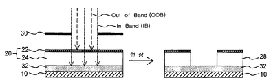
- FIG. 1 is a view for explaining a resist pattern forming method using a photoresist composition according to an embodiment of the present invention.
- the photosensitive polymer according to the present invention is represented by the following formula (1).
- R One are each independently a hydrogen atom (H), a fluorine atom (F), or a methyl group (-CH 3 ), A fluorinated alkyl group having 1 to 20 carbon atoms or a hydroxyalkyl group having 1 to 5 carbon atoms
- R 2 Is a linear, branched or cyclic hydrocarbon group having 1 to 10 carbon atoms, preferably a cyclic hydrocarbon group having 5 to 10 carbon atoms, more preferably a cyclic alkylene having 5 to 10 carbon atoms, that is, 2
- X is or (Where n is an integer of 0 to 5, preferably 0 or 1, and the curve indicates a bonding position), and m is 1 or 2 as the number of X.
- R 3 is an acid-sensitive protecting group, that is, a protecting group deprotected by an acid, and a hydrocarbon group having 1 to 40 carbon atoms, preferably an alkyl group having 1 to 20 carbon atoms or 4 to 40 carbon atoms. It is a cycloalkyl group, More preferably, it is a C1-C10 alkyl group or a C5-C20 cycloalkyl group, If necessary, hetero atoms, such as an oxygen atom (O) and a sulfur atom (S), can be included.
- a protecting group deprotected by an acid and a hydrocarbon group having 1 to 40 carbon atoms, preferably an alkyl group having 1 to 20 carbon atoms or 4 to 40 carbon atoms. It is a cycloalkyl group, More preferably, it is a C1-C10 alkyl group or a C5-C20 cycloalkyl group, If necessary, hetero atoms, such as an oxygen atom (O) and
- Y is an oxygen atom (O), NH or a nitrogen atom (N)
- R 2 may further include.
- R 3 and R 4 is a methyl group with a halogen atom, a hydroxy group, a triple such as fluorine atom (F) (CF 3) or the like.
- the repeating unit corresponding to the content ratio a includes a hexafluoroalcohol group (HFA), which is a strong hydrophobic group, so that when the photosensitive polymer is coated, the photosensitive polymer is photographed by HFA. Automatically arranged into the top layer of the resist film. In addition, the HFA also serves to increase the dissolution rate of the photosensitive polymer during development.
- HFA hexafluoroalcohol group
- the preferred structure of the repeating unit corresponding to the content ratio a is as follows.
- the repeating unit corresponding to the content ratio b is a repeating unit including an acid-sensitive protecting group, and the protecting group is deprotected by an acid generated in an exposure region. During the development process, the photosensitive polymer is easily dissolved and removed.
- the repeating unit corresponding to the content ratio b constitutes a photosensitive polymer for a conventional photoresist used in a conventional ArF, immersion lithography process, and the like, and a preferable structure of the repeating unit is as follows.
- the repeating unit corresponding to the content ratio c while passing in-band (IB) light having a wavelength of 13.5 nm in the extreme ultraviolet lithography (EUVL) process, 100 It functions to absorb and block out-of-band (OOB) light having a wavelength in the range of 500 nm, preferably 100 to 300 nm.
- the repeating unit corresponding to the content ratio c is preferably derived from phenolic monomers with or without salts, and the preferred structure is as follows.
- Each monomer forming the repeating unit of Formula 1 may be prepared according to a conventional organic synthesis method, for example, as disclosed in the Republic of Korea Patent Publication No. 10-2009-0072015, US Patent 7,501,222, etc., the hydroxyl group (OH It can be prepared by reacting each functional group (R 2 , R 3 , R 4 ) having a) with (meth) crylic acid, (meth) cryloyl halide and the like.
- the monomer to form a repeating unit having the content ratio of a ( ) The monomer including (wherein R 1 , R 2 , X, m, n are as defined in Formula 1), 4-dimethylaminopyridine (DMAP), as shown in Scheme 1 below
- DMAP 4-dimethylaminopyridine
- the photosensitive polymer represented by Chemical Formula 1 may be prepared by polymerizing respective monomers forming the repeating unit of Chemical Formula 1 by a conventional method, for example, azobis (isobutyronitrile) (AIBN) and the like. May be polymerized in the presence of a conventional polymerization solvent such as a polymerization initiator and tetrahydrofuran (THF).
- a conventional polymerization solvent such as a polymerization initiator and tetrahydrofuran (THF).
- the molar ratio a: b: c of each repeating unit is preferably from 1 to 50: 1 to 50: 1 to 30, preferably from 1 to 30: 1 to 50: It is still more preferable if it is 1-10, For example, it is 1: 1-10: 0.1-5, Preferably it is 1: 1: 1: 0.2-1.
- the ratio of the repeating units represented by a and / or c is too large, the solubility of the polymer by the developer may be poor, causing pattern defects.
- the weight average molecular weight (Mw) of the photosensitive polymer represented by Formula 1 is 1,000 to 100,000, preferably 2,000 to 50,000, more preferably 3,000 to 10,000, and if the weight average molecular weight of the photosensitive polymer is too small, film formation is If it is too large, it may not be dissolved by the developer.
- the photosensitive polymer according to the present invention has a strong hydrophobic group
- the photosensitive polymer according to the present invention is transferred to the upper layer of the film during the photoresist film coating process. Are moved and arranged automatically.
- the photosensitive polymer arranged on the photoresist film absorbs and blocks unnecessary light in the OOB wavelength band by a light absorbing functional group, thereby solving a pattern defect caused by OOB light.
- the photosensitive polymer according to the present invention may form a uniform micropattern by suppressing a pattern uniformity deterioration caused by light of 100 to 500 nm, specifically, 100 to 300 nm, except for EUV wavelength of 13.5 nm. .
- a photosensitive polymer for a photolithography process having an acid sensitive protecting group can be used without limitation, and for example, a repeating unit represented by the following Chemical Formula 2 It can be used a photosensitive polymer comprising a.
- R 1 and R 3 are as defined in Chemical Formula 1.
- the weight average molecular weight of the conventional photosensitive polymer including the repeating unit represented by Formula 2 is usually 1,000 to 100,000, preferably 3,000 to 20,000. If the weight average molecular weight of the photosensitive polymer is less than 1,000 or more than 100,000, there is a concern that the resist pattern may not be formed correctly.
- the content of the photosensitive polymer represented by Chemical Formula 1 according to the present invention is preferably 1 to 30% by weight, more preferably 2 to 20% by weight, still more preferably 3 to 15% by weight based on the total photosensitive polymer. . If the amount of the photosensitive polymer represented by the formula (1) is less than 1% by weight, the OOB light may not be effectively blocked. If the amount of the photosensitive polymer is greater than 30% by weight, the hydrophobic property may be excessive and the solution may not be dissolved in the developer.
- the photoresist composition according to the present invention includes a (whole) photosensitive polymer, a photoacid generator and a solvent including the photosensitive polymer represented by Chemical Formula 1, and may further include various additives as necessary.
- a photoacid generator conventional photoacid generators such as onium salt and organic sulfonic acid may be used without limitation.
- ethylene glycol monoethyl ether ethylene glycol monomethyl ether, diethylene glycol monoethyl ether, propylene glycol monomethyl ether acetate (PGMEA), toluene, xylene, methyl ethyl ketone, cyclohexanone, 2-hydride Ethyl hydroxypropionate, 2-hydroxy-2-methyl ethyl propionate, ethyl ethoxy acetate, ethyl hydroxy acetate, methyl 2-hydroxy-3-methyl butyrate, 3-methoxy-2-methyl propionate, 3- Conventional solvents for photoresist compositions, such as ethyl ethoxy propionate, 3-methoxy 2-methyl propionate, ethyl acetate, and butyl acetate, can be used without limitation.
- the content of the total photosensitive polymer is 1 to 30% by weight, preferably 2 to 15% by weight based on the photoresist composition, and the content of the photoacid generator is 100% by weight of the total photosensitive polymer.
- the amount is preferably 0.1 to 40 parts by weight, more preferably 2 to 15 parts by weight, and the remaining components are solvents.
- the content of the photosensitive polymer and the photoacid generator is outside the above range, there is a fear that the photoresist pattern is poor.
- the photoresist composition according to the present invention is preferably 0.1 to 10 parts by weight, more preferably 0.5 to 5 parts by weight of organic base (acid diffusion inhibitor (Quencher)) based on 100 parts by weight of the total photosensitive polymer.
- the organic base may include triethylamine, triisobutylamine, triisooctylamine, diethanolamine, triethanolamine, mixtures thereof, and the like.
- the photoresist composition according to the present invention can be prepared by combining the respective components, for example, in the total photoresist composition, each component is mixed so that the concentration of the solid content is 1 to 30% by weight, which is 0.2 ⁇ m It can be used by filtering with a filter.
- FIG. 1 is a view for explaining a resist pattern forming method using a photoresist composition according to the present invention.
- the photoresist composition of the present invention is applied to a substrate 10 such as a silicon wafer or an aluminum substrate using a coating apparatus such as a spin coater, and dried to form a photoresist (PR) film ( 20).
- PR photoresist
- the photosensitive polymer having a strong hydrophobic group represented by the formula (1) is automatically moved and arranged above the film 20 to form the upper photoresist film 22, the general photosensitive The polymer forms the lower photoresist film 24.
- the mask 30 When the mask 30 is mounted on the photoresist (PR) film 20 formed as described above and irradiated with in-band (IB) light having a wavelength of 13.5 nm and out-of-band (OOB) light having a wavelength of 100 to 500 nm,
- IB in-band
- OOB out-of-band
- the out-of-band (OOB) light is blocked by the upper photoresist film 22, while the in-band (IB) light passes through the upper photoresist film 22, so that the entire photoresist film 20 It exposes.
- the photoresist film 20 exposed in this manner is cleaned with baking and ultrapure water as necessary for development and necessity, the photoresist pattern 28 can be formed in which the influence of out-of-band (OOB) light is eliminated.
- OOB out-of-band
- reference numeral 32 denotes an HMDS (hexamethyldisilazane) film which is formed on the substrate 10 as needed to improve the adhesion between the light reflection prevention film or the photoresist film 20 and the substrate 10.
- an alkaline aqueous solution in which alkaline compounds such as sodium hydroxide, potassium hydroxide, sodium carbonate and tetramethylammonium hydroxide (TMAH) are dissolved at a concentration of 0.1 to 10% by weight can be used.
- TMAH tetramethylammonium hydroxide
- an appropriate amount of a water-soluble organic solvent and a surfactant such as methanol and ethanol may be added to the developer.
- a magnetic stirring bar was placed in a 500 ml flask, and 3,5-bis (hexafluoro-2-hydroxy-2-propyl) cyclohexyl methacrylate (3,5-bis (hexafluoro-2) was added.
- -hydroxy-2-propyl) cyclohexyl methacrylate 100g (0.2mol), di-tert-butyldicarbonate 94.06g (0.422mol), 4-dimethylaminopyridine (DMAP) 4.79 g (0.038 mol) and 600 ml of tetrahydrofuran (THF) were added, followed by reaction at room temperature for 20 hours.
- DMAP 4-dimethylaminopyridine
- the weight average molecular weight (Mw) and polydispersity (PD) of the obtained terpolymer were 8,500 and 1.8, respectively.
- the monomers obtained in Preparation Example 1 were used in the combinations described in Tables 1 to 4 below, wherein the molar ratio a: b: c of each monomer was adjusted to 35:50:15, and azobis (isobutyro) as an initiator.
- Nitrile) (AIBN) was used in an amount of 10 parts by weight based on 100 parts by weight of the total monomers, and 300 parts by weight of tetrahydrofuran (THF) was used as the reaction solvent, and the polymerization reaction temperature was 70 ° C., reaction time.
- a photosensitive polymer (terpolymer) was prepared in the same manner as in Preparation Example 2, except that silver was adjusted to 12 hours.
- the weight average molecular weight (Mw), polydispersity (PD) and yield of the obtained photosensitive polymer were measured and shown in Tables 1-4.
- a spin coater to form a 33 nm thick antireflective film by coating DARC-A125 (manufactured by Dongjin Semichem) on a silicon substrate, a photoresist film having a thickness of 60 nm using the photoresist (PR) composition Formed.
- the curing (curing) temperature of the anti-reflective film was 220 °C, after baking the photoresist (PR) composition (Soft Bake: SOB) process was performed for 60 seconds at 115 °C.
- the obtained photoresist film was subjected to EUVL exposure process using an AST ADT (product name) exposure machine (0.25 NA, 0.5 sigma), followed by a post exposure bake (PEB) process at 125 ° C. for 60 seconds. It was then developed for 30 seconds with an aqueous 2.38 wt% tetramethylammonium hydroxide (TMAH) solution to form a resist pattern.
- EUVL exposure process using an AST ADT (product name) exposure machine (0.25 NA, 0.5 sigma), followed by a post exposure bake (PEB) process at 125 ° C. for 60 seconds. It was then developed for 30 seconds with an aqueous 2.38 wt% tetramethylammonium hydroxide (TMAH) solution to form a resist pattern.
- AST ADT product name
- PEB post exposure bake
- Photoresist compositions were prepared in the same manner as in Examples 2-1 to 2-64 except that only the usual EUVL photosensitive polymer obtained in Production Example 2 was used as the photosensitive polymer, to form a resist pattern.
- the thickness of the photoresist film was 60 nm
- the bake (SOB) after coating was 115 ° C.
- the bake after exposure (PEB) was carried out at 125 °C
- EOP Esnergy of Optimization, 30 nm pattern embodied positive energy
- the thickness of each membrane was measured by Opti-2600, a measuring instrument of KLA (Japan), and EOP was measured using Hitachi S9220 CD-SEM equipment of Hitachi, Japan.
- the line width roughness (LWR) was measured using Hitachi S9220 CD-SEM equipment manufactured by Hitachi, Japan, and the results are shown in Tables 5 to 8.
- a photoresist composition comprising a photosensitive polymer according to the present invention (photosensitive polymer obtained by blending a typical photosensitive polymer for EUVL and the photosensitive polymer represented by Formula 1) (Example 2-1 To 2-64) to prepare a photoresist pattern, compared with the case of using a photoresist composition (comparative example) containing only a conventional photosensitive polymer, there is no change in EOP, but effectively block OOB light, It can be seen that the surface roughness (LWR) of the resist pattern is reduced.
- a photosensitive polymer according to the present invention photosensitive polymer obtained by blending a typical photosensitive polymer for EUVL and the photosensitive polymer represented by Formula 1
- the photoresist composition according to the present invention allows LWR to be reduced by effectively suppressing the transmission of OOB light, which is a distorted wavelength, into the resist without passing in-band (IB, 13.5 nm) light and changing the sensitivity of the resist. It can be seen that the improvement.
- the photosensitive polymer according to the present invention, a photoresist composition comprising the same, and a method of forming a resist pattern using the same are useful for forming a fine pattern of a semiconductor device using an extreme ultraviolet lithography (EUVL) process.
- EUVL extreme ultraviolet lithography
Landscapes
- Physics & Mathematics (AREA)
- Spectroscopy & Molecular Physics (AREA)
- General Physics & Mathematics (AREA)
- Engineering & Computer Science (AREA)
- Microelectronics & Electronic Packaging (AREA)
- Computer Hardware Design (AREA)
- Manufacturing & Machinery (AREA)
- Power Engineering (AREA)
- Condensed Matter Physics & Semiconductors (AREA)
- Chemical & Material Sciences (AREA)
- Ceramic Engineering (AREA)
- Addition Polymer Or Copolymer, Post-Treatments, Or Chemical Modifications (AREA)
- Materials For Photolithography (AREA)
- Exposure And Positioning Against Photoresist Photosensitive Materials (AREA)
Abstract
반도체 소자 형성을 위한 포토리쏘그래피 공정에서, 극자외선(Extreme ultraviolet; EUV) 파장의 광은 통과시키되, 극자외선 보다 장파장의 광은 차단시키는 감광성 고분자, 이를 포함하는 포토레지스트 조성물 및 이를 이용한 레지스트 패턴 형성방법이 개시된다. 상기 감광성 고분자는 청구항 1의 화학식 1로 표시된다.
Description
본 발명은 감광성 고분자에 관한 것으로서, 더욱 상세하게는, 반도체 소자 형성을 위한 포토리쏘그래피 공정에서, 극자외선(Extreme ultraviolet; EUV) 파장의 광은 통과시키되, 극자외선 보다 장파장의 광은 차단시키는 감광성 고분자, 이를 포함하는 포토레지스트 조성물 및 이를 이용한 레지스트 패턴 형성방법에 관한 것이다.
최근, 반도체 소자의 소형화 및 집적화에 따라, 반도체 소자 형성을 위한 레지스트 패턴이 미세화되고 있다. 레지스트 패턴의 미세화를 위해서는, 노광원의 파장이 작아져야 하고, 현재는 13.5 nm 파장의 노광원을 이용하는 극자외선 리소그라피(Extreme ultraviolet lithography; EUVL) 기술을 이용하여, 30 nm 급의 반도체 소자를 제조하고 있다. 이와 같은 레지스트 패턴의 미세화에 따라, 여러 가지 문제점들이 발생하고 있으며, 예를 들면, 레지스트 패턴 불량, 스컴(scum) 발생, LWR(line width or edge roughness) 수치 증가, 패턴 쓰러짐 등과 같은 흠결(defect)이 발생하여, 반도체 소자의 생산 수율을 저하시킨다. 따라서, 레지스트 패턴의 미세화에 따른 각종 문제를 해결하기 위하여, 레지스트 재료를 개선하는 등의 다양한 대응 기술이 개발되고 있다.
극자외선 리소그라피(EUVL) 공정에서는, 광원에서 13.5 nm의 인밴드(in band; IB) 파장의 광뿐만 아니라 아웃 오브 밴드(out of band; OOB) 파장의 광이 발생하여, 패턴의 해상력 저하, 프로파일 왜곡, 표면 거칠기 심화 등을 야기한다. 즉, 현재의 EUVL 공정에서는, 사용하고자 하는 13.5 nm 파장의 광 이외에, 약 5% 정도의 100 내지 300 nm 영역의 파장대를 갖는 아웃 오브 밴드(OOB) 광도 동시에 방출되므로, 아웃 오브 밴드(OOB) 광에 의한 악영향을 제거할 필요가 있다(Proc. of SPIE Vol. 7273, 1W, 2009). 또한, EUVL 공정에 있어서는, 최종 반도체 소자(회로)의 성능을 결정하는 중요한 변수로서, 패턴의 표면 거칠기에 해당하는 LWR(Line Width Roughness)을 면밀히 관리하여야 한다.
본 발명의 목적은, 광원에서 발생하는 아웃 오브 밴드(OOB) 광을 차단하여, 아웃 오프 밴드 광에 의한 문제를 감소시킬 수 있는 감광성 고분자를 제공하는 것이다. 본 발명의 다른 목적은, 레지스트 패턴의 LWR을 개선할 수 있는 감광성 고분자, 이를 포함하는 포토레지스트 조성물 및 이를 이용한 레지스트 패턴 형성방법을 제공하는 것이다.
상기 목적을 달성하기 위하여, 본 발명은, 하기 화학식 1로 표시되는 감광성 고분자를 제공한다.
[화학식 1]

상기 화학식 1에서, R1은 각각 독립적으로 수소 원자(H), 불소 원자(F), 메틸기(-CH3), 탄소수 1 내지 20의 불소화 알킬기 또는 탄소수 1 내지 5의 히드록시알킬기이고, R2는 탄소수 1 내지 10의 사슬형, 분지형 또는 고리형 탄화수소기이고, R3는 산에 의하여 탈보호되는 보호기로서, 탄소수 1 내지 40의 탄화수소기이고, R4는 하나 이상의 방향족 고리를 포함하는 탄소수 6 내지 40의 탄화수소기이며, X는  또는
또는  (여기서, n은 0 내지 5의 정수이며, 굴곡선은 결합부위를 나타낸다)이고, Y는 산소 원자(O), NH 또는 질소 원자(N)이고, m은 X의 개수로서, 1 또는 2이며, a, b 및 c는 상기 고분자를 구성하는 반복단위의 몰비율(molar ratio)로서, a : b : c는 1~50 : 1~50 : 1~30이다.
본 발명에 따른 감광성 고분자는, 광원에서 발생하는 아웃 오브 밴드(OOB) 광을 차단하여, 아웃 오프 밴드 광에 의한 문제를 감소시킬 뿐만 아니라, 레지스트 패턴의 LWR을 개선할 수 있다.
도 1은 본 발명의 일실시예에 따른 포토레지스트 조성물을 사용한 레지스트 패턴 형성 방법을 설명하기 위한 도면.
도 2는 본 발명의 제조예 1에 따라 제조된 화학식 c-33으로 표시되는 반복단위 형성 모노머의 H-NMR 데이터.
이하, 본 발명을 상세히 설명하면 다음과 같다.
본 발명에 따른 감광성 고분자는 하기 화학식 1로 표시된다.
[화학식 1]

상기 화학식 1에서, R1은 각각 독립적으로 수소 원자(H), 불소 원자(F), 메틸기(-CH3), 탄소수 1 내지 20의 불소화 알킬기 또는 탄소수 1 내지 5의 히드록시알킬기이고, R2는 탄소수 1 내지 10의 사슬형, 분지형 또는 고리형 탄화수소기로서, 바람직하게는 탄소수 5 내지 10의 고리형 탄화수소기, 더욱 바람직하게는 탄소수 5 내지 10의 고리형 알킬렌(alkylene, 즉, 2가(divalent) 고리형 알킬기, m이 1인 경우)기 또는 알킬리딘(alkylidyne, 즉, 3가(trivalent) 고리형 알킬기, m이 2인 경우)기이고, X는  또는
또는  (여기서, n은 0 내지 5의 정수, 바람직하게는 0 또는 1이며, 굴곡선은 결합 위치를 나타낸다.)이며, m은 X의 개수로서, 1 또는 2이다.
상기 화학식 1에서, R3는 산에 민감한 보호기, 즉, 산에 의하여 탈보호(deprotection)되는 보호기로서, 탄소수 1 내지 40의 탄화수소기, 바람직하게는 탄소수 1 내지 20의 알킬기 또는 탄소수 4 내지 40의 사이클로알킬기이며, 더욱 바람직하게는 탄소수 1 내지 10의 알킬기 또는 탄소수 5 내지 20의 사이클로알킬기로서, 필요에 따라, 산소 원자(O), 황 원자(S) 등의 이종 원자를 포함할 수 있다. 또한, 상기 화학식 1에서, Y는 산소 원자(O), NH 또는 질소 원자(N)이고, R4는 하나 이상의 방향족 고리를 포함하는 탄소수 6 내지 40의 탄화수소기로서, 바람직하게는, 탄소수 6 내지 40의 아릴(aryl)기 또는 아르알킬(aralkyl)기, 탄소수 6 내지 40의 아릴(aryl) 설포닐기(-S(=O)2-) 또는 아르알킬(aralkyl) 설포닐기(-S(=O)2-)이며, 필요에 따라, 산소 원자(O), 황 원자(S) 등의 이종 원자, -SO3
-S+- 등의 설포늄염(sulfonium salt), 아이오도늄염(iodonium salt) 등을 더욱 포함할 수 있다. 또한, 필요에 따라, 상기 R2, R3 및 R4는 불소 원자(F) 등의 할로겐 원자, 히드록시기, 트리플로로메틸기(CF3) 등으로 치환되어 있을 수 있다.
상기 화학식 1로 표시되는 감광성 고분자에 있어서, 함량 비율 a에 해당하는 반복단위는 강한 소수성기인 헥사플루오르알코올기(hexafluoroalcohol; HFA)를 포함하므로, 감광성 고분자의 코팅 시, HFA에 의해, 감광성 고분자가 포토레지스트 필름의 상부 층으로 자동적으로 배열된다. 또한, 상기 HFA는 현상(development) 과정에서 감광성 고분자의 용해속도를 증가시키는 기능도 수행한다. 상기 함량 비율 a에 해당하는 반복단위의 바람직한 구조는 다음과 같다.


상기 화학식 1로 표시되는 감광성 고분자에 있어서, 함량 비율 b에 해당하는 반복단위는 산에 민감한 보호기를 포함하는 반복단위로서, 노광 영역에서 발생한 산(acid)에 의하여 보호기가 탈보호(deprotecting)되어, 현상 과정에서 감광성 고분자가 쉽게 용해 및 제거되도록 한다. 상기 함량 비율 b에 해당하는 반복단위는 통상의 ArF, 액침(immersion) 리소그래피 공정 등에 사용되는 통상의 포토레지스트용 감광성 고분자를 구성하는 것으로서, 상기 반복단위의 바람직한 구조는 다음과 같다.


또한, 상기 화학식 1로 표시되는 감광성 고분자에 있어서, 함량 비율 c에 해당하는 반복단위는, 극자외선 리소그라피(EUVL) 공정에서, 13.5 nm의 파장을 가지는 인밴드(IB) 광은 통과시키는 반면, 100 내지 500 nm, 바람직하게는 100 내지 300 nm 영역의 파장을 가지는 아웃 오브 밴드(OOB) 광을 흡수하여 차단하는 기능을 한다. 상기 함량 비율 c에 해당하는 반복단위는, 바람직하게는 염을 포함하거나 포함하지 않는 페놀류 단량체로부터 유도된 것으로서, 바람직한 구조는 다음과 같다.


상기 화학식 1의 반복단위를 형성하는 각각의 모노머들은 통상의 유기 합성법에 따라 제조될 수 있고, 예를 들면, 대한민국 특허공개 10-2009-0072015호, 미국특허 7,501,222호 등에 개시된 바와 같이, 히드록시기(OH)를 가지는 각각의 작용기(R2, R3, R4)와 (메타)크릴산, (메타)크릴로일할라이드 등을 반응시켜 제조될 수 있다. 또한, 상기 함량 비율이 a인 반복단위를 형성하는 모노머( ) 중,
) 중,  (여기서, R1, R2, X, m, n은 상기 화학식 1에서 정의한 바와 같다)을 포함하는 모노머는, 하기 반응식 1에 나타낸 바와 같이, 4-디메틸아미노피리딘(4-Dimethylaminopyridine: DMAP)을 촉매로 사용하고, 테트라하이드로퓨란(THF)을 용매로 사용하여, 헥사플루오르알코올기 등을 포함하는 모노머, 예를 들면, 3,5-비스(헥사플루오르-2-히드록시-2-프로필)시클로헥실 메타크릴레이트(3,5-bis(hexafluoro-2-hydroxy-2-propyl)cyclohexyl methacrylate)의 히드록시기(-OH)와 디-tert-부틸디카보네이트(di-tert-butyl dicarbonate)를 반응시켜 얻을 수 있다.
[반응식 1]

상기 화학식 1로 표시되는 감광성 고분자는, 화학식 1의 반복단위를 형성하는 각각의 모노머들을 통상의 방법으로 중합하여 제조될 수 있으며, 예를 들어, 아조비스(이소부티로니트릴)(AIBN) 등 통상의 중합개시제와 테트라하이드로퓨란(THF) 등 통상의 중합 용매의 존재 하에서, 중합될 수 있다.
상기 화학식 1로 표시되는 감광성 고분자에 있어서, 각 반복단위의 몰비율(mole ratio) a : b : c는 1~50 : 1~50 : 1~30이 바람직하고, 1~30 : 1~50 : 1~10이면 더욱 바람직하며, 예를 들면, 1 : 1~10 : 0.1~5, 바람직하게는 1 : 1~5 : 0.2~1이다. 여기서, 상기 a 및/또는 c로 표시되는 반복단위의 비율이 너무 많으면, 현상액에 의한 고분자의 용해도가 떨어져 패턴 불량을 유발할 수 있고, a로 표시되는 반복단위의 비율이 너무 적으면, 감광성 고분자가 포토레지스트 필름의 상부층으로 이동되지 않을 우려가 있고, c로 표시되는 반복단위의 비율이 너무 적으면, 아웃 오브 밴드(OOB) 광의 흡수 효율이 저하될 우려가 있다. 상기 화학식 1로 표시되는 감광성 고분자의 중량평균분자량(Mw)은 1,000 내지 100,000, 바람직하게는 2,000 내지 50,000, 더욱 바람직하게는 3,000 내지 10,000이며, 상기 감광성 고분자의 중량평균분자량이 너무 작으면 필름 형성이 되지 않을 우려가 있고, 너무 크면 현상액에 의해서 용해되지 않을 우려가 있다.
본 발명에 따른 감광성 고분자는 강한 소수성기를 가지므로, 통상의 감광성 고분자와 혼합하여(blending) 포토레지스트(PR) 필름을 형성하면, 포토레지스트 필름 코팅 과정에서, 본 발명에 따른 감광성 고분자가 필름 상부층으로 자동적으로 이동 및 배열된다. 이와 같이 포토레지스트 필름 상부에 배열된 감광성 고분자는 흡광성 작용기에 의하여 OOB 파장대의 불필요한 광을 흡수 및 차단하여, OOB 광에 의한 패턴 불량을 해결할 수 있다. 즉, 본 발명에 따른 감광성 고분자는, 13.5 nm의 EUV 파장을 제외한, 100 내지 500 nm, 구체적으로는 100 내지 300 nm의 광에 의한 패턴 균일도 저하 현상을 억제하여 균일한 미세패턴을 형성할 수 있다.
본 발명에 따른 감광성 고분자와 함께 사용될 수 있는 통상의 감광성 고분자로는 산에 민감한 보호기를 가지는 통상의 포토리쏘그래피 공정용 감광성 고분자를 제한 없이 사용할 수 있으며, 예를 들면 하기 화학식 2로 표시되는 반복단위를 포함하는 감광성 고분자를 사용할 수 있다.
[화학식 2]

상기 화학식 2에서, R1 및 R3은 화학식 1에서 정의한 바와 같다. 상기 화학식 2로 표시되는 반복단위를 포함하는 통상적인 감광성 고분자의 중량평균분자량은 통상 1,000 내지 100,000, 바람직하게는 3,000 내지 20,000이다. 상기 감광성 고분자의 중량평균분자량이 1,000 미만이거나, 100,000을 초과하면, 레지스트 패턴이 올바로 형성되지 못할 우려가 있다. 본 발명에 따른 화학식 1로 표시되는 감광성 고분자의 함량은, 전체 감광성 고분자에 대하여 바람직하게는 1 내지 30 중량%이며, 더욱 바람직하게는 2 내지 20 중량%, 더더욱 바람직하게는 3 내지 15 중량% 이다. 화학식 1로 표시되는 감광성 고분자의 혼합량이 1중량% 미만이면 OOB 광을 효과적으로 차단할 수 없으며, 30 중량%를 초과하면, 소수성 특성이 과도하여, 현상액에 용해되지 않을 우려가 있다.
본 발명에 따른 포토레지스트 조성물은, 상기 화학식 1로 표시되는 감광성 고분자를 포함하는 (전체) 감광성 고분자, 광산발생제 및 용매를 포함하며, 필요에 따라 각종 첨가제를 더욱 포함할 수 있다. 상기 광산발생제로는 오니움 염, 유기 술폰산 등 통상의 광산발생제를 제한 없이 사용할 수 있다. 또한, 상기 용매로는 에틸렌글리콜모노에틸에테르, 에틸렌글리콜모노메틸에테르, 디에틸렌글리콜모노에틸에테르, 프로필렌글리콜모노메틸에테르아세테이트(PGMEA), 톨루엔, 크실렌, 메틸에틸케톤, 시클로헥산온, 2-히드록시프로피온에틸, 2-히드록시-2-메틸 프로피온산에틸, 에톡시초산에틸, 히드록시초산에틸, 2-히드록시-3-메틸부탄산메틸, 3-메톡시-2-메틸프로피온산메틸, 3-에톡시프로피온산에틸, 3-메톡시 2-메틸프로피온산에틸, 초산에틸, 초산부틸 등, 통상의 포토레지스트 조성물용 용매를 제한 없이 사용할 수 있다. 본 발명에 따른 포토레지스트 조성물에 있어서, 전체 감광성 고분자의 함량은, 포토레지스트 조성물에 대하여 1 내지 30 중량%, 바람직하게는 2 내지 15 중량%이며, 상기 광산발생제의 함량은 전체 감광성 고분자 100 중량부에 대하여 바람직하게는 0.1 내지 40 중량부, 더욱 바람직하게는 2 내지 15 중량부이며, 나머지 성분은 용매이다. 여기서, 상기 감광성 고분자 및 광산발생제의 함량이 상기 범위를 벗어나면, 포토레지스트 패턴이 불량해질 우려가 있다. 또한, 필요에 따라, 본 발명에 따른 포토레지스트 조성물은, 전체 감광성 고분자 100 중량부에 대하여 바람직하게는 0.1 내지 10 중량부, 더욱 바람직하게는 0.5 내지 5 중량부의 유기염기(산확산 억제제(Quencher))를 더욱 포함할 수 있으며, 상기 유기염기로는 트리에틸아민, 트리이소부틸아민, 트리이소옥틸아민, 디에탄올아민, 트리에탄올아민, 이들의 혼합물 등을 예시할 수 있다. 본 발명에 따른 포토레지스트 조성물은 각각의 성분을 배합하여 제조될 수 있으며, 예를 들면, 전체 포토레지스트 조성물에 있어서, 고형분의 농도가 1 내지 30 중량%가 되도록 각 성분을 혼합하고, 이를 0.2 ㎛ 필터로 여과하여 사용할 수 있다.
도 1은 본 발명에 따른 포토레지스트 조성물을 사용한 레지스트 패턴 형성 방법을 설명하기 위한 도면이다. 도 1에 도시한 바와 같이, 먼저, 스핀 코터 등의 코팅 장비를 이용하여, 실리콘 웨이퍼, 알루미늄 기판 등의 기판(10)에 본 발명의 포토레지스트 조성물을 도포하고 건조하여 포토레지스트(PR) 필름(20)을 형성한다. 상기 포토레지스트 필름(20)의 형성 과정에서, 화학식 1로 표시되는 강한 소수성기를 가지는 감광성 고분자는 필름(20) 상부로 자동적으로 이동 및 배열되어 상부 포토레지스트 필름(22)을 형성하고, 통상의 감광성 고분자는 하부 포토레지스트 필름(24)을 형성한다. 이와 같이 형성된 포토레지스트(PR) 필름(20) 상부에 마스크(30)를 장착하고, 13.5 nm 파장의 인밴드(IB) 광과 100 내지 500 nm 파장의 아웃 오브 밴드(OOB) 광을 조사하면, 상기 아웃 오브 밴드(OOB) 광은 상부 포토레지스트 필름(22)에 의하여 차단되는 반면, 상기 인밴드(IB) 광은 상부 포토레지스트 필름(22)을 통과하여, 상기 포토레지스트 필름(20) 전체를 노광시킨다. 이와 같이 노광된 포토레지스트 필름(20)을 현상 및 필요에 따라 베이크 및 초순수로 세정하면, 아웃 오브 밴드(OOB) 광의 영향이 배제된, 포토레지스트 패턴(28)을 형성할 수 있다. 도 1에 있어서, 도면 부호 32는, 필요에 따라 기판(10) 상부에 형성되는, 광반사방지막 또는 포토레지스트 필름(20)과 기판(10)의 접착력을 향상시켜주는 HMDS(hexamethyldisilazane) 막이다. 상기 현상 공정에 사용되는 현상액으로는 수산화나트륨, 수산화칼륨, 탄산나트륨, 테트라메틸암모늄히드록사이드(TMAH) 등의 알칼리성 화합물을 0.1 내지 10중량%의 농도로 용해시킨 알칼리 수용액을 사용할 수 있다. 또한, 상기 현상액에는 메탄올, 에탄올 등과 같은 수용성 유기용매 및 계면활성제를 적정량 첨가할 수 있다.
이하, 구체적인 실시예 및 비교예를 통하여 본 발명을 더욱 상세히 설명한다. 하기 실시예는 본 발명을 예시하기 위한 것으로서, 본 발명이 하기 실시예에 의해 한정되는 것은 아니다.
[제조예 1] 모노머의 제조
1. 화학식 a-4로 표시되는 반복단위 형성 모노머의 제조
상기 반응식 1에 나타낸 바와 같이, 500ml 플라스크에 자석 교반 막대를 넣고, 3,5-비스(헥사플루오르-2-히드록시-2-프로필)시클로헥실 메타크릴레이트(3,5-bis(hexafluoro-2-hydroxy-2-propyl)cyclohexyl methacrylate) 100g(0.2mol), 디-tert-부틸디카보네이트(di-tert-butyldicarbonate) 94.06g (0.422mol), 4-디메틸아미노피리딘(4-dimethylaminopyridine: DMAP) 4.79g(0.038mol) 및 테트라히드로퓨란(THF) 600ml을 첨가한 후, 상온에서 20시간 동안 반응시켰다. 반응이 완결된 후, 감압 하에서 테트라히드로퓨란을 제거하여 화학식 a-4로 표시되는 반복단위를 형성하는 모노머 134.6g을 얻었다{수율: 96%, NMR: CH3(1.93, 1.4), CH2(1.64, 1.36), CH(3.91, 2.01), H(6.15, 5.58)}.
2. 화학식 c-17로 표시되는 반복단위 형성 모노머의 제조
4-(트리플루오르메틸)벤질알코올(4-(trifluoromethyl)benzylalcohol) 0.28 mol (49.32 g)과 트리에틸아민 0.32 mol(44.48 ml)을 메틸렌클로라이드(MC) 300 ml에 용해시킨 후, 적하 깔대기를 이용하여 메타크릴로일클로라이드 0.32 mol(26 ml)를 천천히 첨가하고, 실온에서 12시간 동안 반응시켰다. 반응이 완결된 후, 로터리 증발기(evaporator)를 사용하여 과량의 MC를 제거하고, 생성물을 물에 부었다. 생성물을 묽은 염산으로 중화하고, 디에틸에테르로 추출한 다음, 무수 마그네슘 설페이트로 건조하여, 화학식 c-17로 표시되는 반복단위 형성 모노머를 얻었다{수율: 72%, NMR: CH3(2.01), CH2(5.16), CH(7.55, 7.16), H(6.48, 6.40)}.
3. 화학식 c-33로 표시되는 반복단위 형성 모노머의 제조
하기 반응식 2에 따라, 화학식 c-33으로 표시되는 반복단위 형성 모노머를 얻었으며(수율: 50%), 얻어진 모노머의 H-NMR 데이터를 도 2에 나타내었다. 하기 반응식 2에서, TEA는 트리에틸아민을 나타내고, RT는 실온(room temperature)를 나타낸다.
[반응식 2]

4. 기타, 상기 항목 1 내지 3에 개시된 방법 또는 히드록시기를 포함하는 작용기와 (메타)크릴산 또는 (메타)크릴로일할라이드를 반응시키는 방법을 따르거나, 시판되는 제품을 구입하여, 화학식 a-1(제조사: Central Glass, 일본), a-13(제조사: Central Glass, 일본), a-16(제조사: Central Glass, 일본), b-3(제조사: 오사카 유키, 일본), c-1, c-3 등으로 표시되는 반복단위 형성 모노머를 얻었다.
[제조예 2] 통상의 EUVL용 감광성 고분자의 제조
2-메틸-2-아다만틸메타크릴레이트 117.2 g(0.5 mol), 3-히드록시-1-아다만틸 메타크릴레이트 23.6 g(0.1 mol), 노보닐락톤 메타크릴레이트(제조사: 오사카 유키, 일본, 제품명: MNBL, 5-oxo-4-oxatricyclo[4,2,1,0] nonan-2-yl methacrylate) 88.9 g(0.4 mol) 및 아조비스(이소부티로니트릴)(AIBN) 6.6 g을 무수 테트라히드로퓨란(THF) 125 g에 용해시키고, 동결방법으로 앰플(ampoule)을 사용하여 가스를 제거한 후, 68 ℃에서 24시간 동안 중합시켰다. 반응이 완결된 후, 과량의 디에틸에테르에 반응물을 천천히 떨어뜨려 침전시키고, 다시 THF에 용해시킨 후, 디에틸에테르에서 재침전시켜 터폴리머(수율: 53%)를 얻었다. 얻어진 터폴리머의 중량평균분자량 (Mw)과 다중분산도(Polydispersity: PD)는 각각 8,500 및 1.8이었다.
[실시예 1-1 내지 1-64] 감광성 고분자의 제조
상기 제조예 1에서 얻어진 모노머들을 하기 표 1 내지 4에 개시된 조합으로 사용하고(여기서, 각 단량체의 몰비율 a : b : c는 35 : 50 : 15로 조절), 개시제로서 아조비스(이소부티로니트릴)(AIBN)을 전체 단량체 100 중량부에 대하여 10 중량부 사용하고, 반응 용매로서 테트라히드로퓨란(THF)을 전체 단량체 100중량부에 대하여 300중량부 사용한 것과 중합 반응 온도는 70 ℃, 반응 시간은 12시간으로 조절한 것을 제외하고는, 상기 제조예 2와 동일한 방법으로 감광성 고분자(터폴리머)를 제조하였다. 얻어진 감광성 고분자의 중량평균분자량(Mw), 다중분산도(PD) 및 수율을 측정하여 표 1 내지 4에 나타내었다.
표 1 
표 2 
표 3 
표 4 
[실시예 2-1 내지 2-64] 포토레지스트 조성물 제조 및 레지스트 패턴 형성
제조예 2에서 얻어진 통상의 EUVL용 감광성 고분자와 실시예 1-1 내지 1-64에서 얻어진 감광성 고분자를 90 : 10의 중량비로 혼합한(blending) (전체) 감광성 고분자, 전체 감광성 고분자 100 중량부에 대하여, 10 중량부의 광산발생제(PAG, 트리페닐설포늄 노나플레이트(TPS-Nf)), 전체 감광성 고분자 100 중량부에 대하여, 2 중량부의 산확산 억제제(Quencher, 트리에탄올아민) 및 용매로서 전체 감광성 고분자 100 중량부에 대하여, 2000 중량부의 프로필렌글리콜 모노메틸에테르 아세테이트(PGMEA)를 혼합하고, 6시간 동안 교반하여 각 성분을 완전히 용해시킨 후, 구멍 크기가 0.01 마이크로미터인 나일론 재질의 필터와 폴리테트라플루오로에틸렌(polytetrafluoroethylene: PTFE) 재질의 필터를 순차적으로 통과시켜, 포토레지스트(PR) 조성물을 제조하였다(실시예 2-1 내지 2-64).
스핀 코터를 사용하여, 실리콘 기판에 DARC-A125(제조사: 동진쎄미켐)을 코팅시킴으로써 33 nm 두께의 광반사방지막을 형성한 후, 상기 포토레지스트(PR) 조성물을 사용하여 60 nm 두께의 포토레지스트 필름을 형성하였다. 이때, 상기 광반사방지막의 큐어링(curing) 온도는 220℃이었고, 포토레지스트(PR) 조성물 코팅 후 베이크(Soft Bake: SOB) 공정은 115℃에서 60초 동안 수행되었다. 얻어진 포토레지스트 필름에 대하여, ASML사의 ADT(제품명) 노광기(0.25 NA, 0.5시그마)를 사용하여 EUVL 노광 공정을 진행하고, 125℃에서 60초 동안 노광 후 베이크(Post Exposure Bake; PEB) 공정을 수행한 다음, 2.38중량% 테트라메틸암모늄히드록사이드 (TMAH) 수용액으로 30초 동안 현상하여, 레지스트 패턴을 형성하였다.
[비교예] 포토레지스트 조성물 제조 및 레지스트 패턴 형성
감광성 고분자로서, 제조예 2에서 얻어진 통상의 EUVL용 감광성 고분자 만을 사용한 것을 제외하고는, 실시예 2-1 내지 2-64와 동일한 방법으로, 포토레지스트 조성물을 제조하고, 레지스트 패턴을 형성하였다.
실시예 2-1 내지 2-64 및 비교예의 레지스트 패턴 형성에 있어서, 포토레지스트 필름 두께(Thickness of PR: TPR)는 60 nm였고, 코팅 후 베이크(SOB)는 115℃, 노광 후 베이크(PEB)는 125℃에서 수행되었으며, EOP(Energy of Optimization, 30 nm 패턴 구현되는 정에너지)는 10.2 mJ였다. 각 막의 두께는 KLA사(일본)의 계측장비인 Opti-2600으로 측정하였고, EOP는 일본 히타치사의 Hitachi S9220 CD-SEM 장비를 사용하여 측정하였다. 또한, 일본 히타치사의 Hitachi S9220 CD-SEM 장비를 사용하여 LWR(line width roughness)을 측정하고, 그 결과를 표 5 내지 8에 나타내었다.
표 5 
표 6 
표 7 
표 8 
상기 실시예 및 비교예로부터, 본 발명에 따른 감광성 고분자(통상의 EUVL용 감광성 고분자와 화학식 1로 표시되는 감광성 고분자를 혼합(blending)한 감광성 고분자)를 포함하는 포토레지스트 조성물(실시예 2-1 내지 2-64)을 사용하여 포토레지스트 패턴을 제조하면, 통상의 감광성 고분자만을 포함하는 포토레지스트 조성물(비교예)을 사용하는 경우와 비교하여, EOP의 변화는 없으나, OOB광을 효과적으로 차단하여, 레지스트 패턴의 표면거칠기(LWR)가 감소시킴을 알 수 있다. 즉, 본 발명에 따른 포토레지스트 조성물은, 인밴드(IB, 13.5 nm) 광은 통과시켜, 레지스트의 감도에 변화를 주지 않고, 왜곡된 파장인 OOB광의 레지스트로의 투과를 효과적으로 억제함으로써, LWR을 향상시킴을 알 수 있다.
본 발명에 따른 감광성 고분자, 이를 포함하는 포토레지스트 조성물 및 이를 이용한 레지스트 패턴 형성방법은 극자외선 리소그라피(EUVL) 공정을 이용한 반도체 소자의 미세 패턴 형성에 유용하다.
Claims (8)
- 하기 화학식 1로 표시되는 감광성 고분자.[화학식 1]
 상기 화학식 1에서, R1은 각각 독립적으로 수소 원자(H), 불소 원자(F), 메틸기(-CH3), 탄소수 1 내지 20의 불소화 알킬기 또는 탄소수 1 내지 5의 히드록시알킬기이고, R2는 탄소수 1 내지 10의 사슬형, 분지형 또는 고리형 탄화수소기이고, R3는 산에 의하여 탈보호되는 보호기로서, 탄소수 1 내지 40의 탄화수소기이고, R4는 하나 이상의 방향족 고리를 포함하는 탄소수 6 내지 40의 탄화수소기이며, X는또는
 (여기서, n은 0 내지 5의 정수이며, 굴곡선은 결합부위를 나타낸다)이고, Y는 산소 원자(O), NH 또는 질소 원자(N)이고, m은 X의 개수로서, 1 또는 2이며, a, b 및 c는 상기 고분자를 구성하는 반복단위의 몰비율(molar ratio)로서, a : b : c는 1~50 : 1~50 : 1~30이다.
- 제1항에 있어서, 상기 감광성 고분자의 중량평균분자량은 1,000 내지 100,000인 것인 감광성 고분자.
- 상기 화학식 1에서, R2는 탄소수 5 내지 10의 고리형 탄화수소기이고, R3는 탄소수 1 내지 20의 알킬기 또는 탄소수 4 내지 40의 사이클로알킬기이며, R4는 탄소수 6 내지 40의 아릴(aryl)기 또는 아르알킬(aralkyl)기, 탄소수 6 내지 40의 아릴(aryl) 또는 아르알킬(aralkyl) 설포닐기(-S(=O)2-)인 것인 감광성 고분자.
- 하기 화학식 1로 표시되는 감광성 고분자를 포함하는 감광성 고분자 1 내지 30 중량%,[화학식 1]
 상기 화학식 1에서, R1은 각각 독립적으로 수소 원자(H), 불소 원자(F), 메틸기(-CH3), 탄소수 1 내지 20의 불소화 알킬기 또는 탄소수 1 내지 5의 히드록시알킬기이고, R2는 탄소수 1 내지 10의 사슬형, 분지형 또는 고리형 탄화수소기이고, R3는 산에 의하여 탈보호되는 보호기로서, 탄소수 1 내지 40의 탄화수소기이고, R4는 하나 이상의 방향족 고리를 포함하는 탄소수 6 내지 40의 탄화수소기이며, X는또는
 (여기서, n은 0 내지 5의 정수이며, 굴곡선은 결합부위를 나타낸다)이고, Y는 산소 원자(O), NH 또는 질소 원자(N)이고, m은 X의 개수로서, 1 또는 2이며, a, b 및 c는 상기 고분자를 구성하는 반복단위의 몰비율(molar ratio)로서, a : b : c는 1~50 : 1~50 : 1~30이다;
 상기 감광성 고분자 100 중량부에 대하여, 0.1 내지 40 중량부의 광산발생제; 및나머지 용매를 포함하는 포토레지스트 조성물.
 - 제4항에 있어서, 전체 감광성 고분자에서, 상기 화학식 1로 표시되는 감광성 고분자의 함량은 1 내지 30 중량%인 것인 포토레지스트 조성물.
- 제4항에 있어서, 상기 감광성 고분자에서, 상기 화학식 1로 표시되는 감광성 고분자를 제외한 나머지 감광성 고분자는 하기 화학식 2로 표시되는 반복단위를 포함하는 감광성 고분자인 것인 포토레지스트 조성물.[화학식 2]
 상기 화학식 2에서, R1 및 R3은 상기 화학식 1에서 정의한 바와 같다.
 - 기판에 하기 화학식 1로 표시되는 감광성 고분자를 포함하는 감광성 고분자 1 내지 30 중량%; 상기 감광성 고분자 100 중량부에 대하여, 0.1 내지 40 중량부의 광산발생제; 및 나머지 용매를 포함하는 포토레지스트 조성물을 도포하고, 건조(베이크)시켜 포토레지스트(PR) 필름을 형성하는 단계,[화학식 1]
 상기 화학식 1에서, R1은 각각 독립적으로 수소 원자(H), 불소 원자(F), 메틸기(-CH3), 탄소수 1 내지 20의 불소화 알킬기 또는 탄소수 1 내지 5의 히드록시알킬기이고, R2는 탄소수 1 내지 10의 사슬형, 분지형 또는 고리형 탄화수소기이고, R3는 산에 의하여 탈보호되는 보호기로서, 탄소수 1 내지 40의 탄화수소기이고, R4는 하나 이상의 방향족 고리를 포함하는 탄소수 6 내지 40의 탄화수소기이며, X는또는
 (여기서, n은 0 내지 5의 정수이며, 굴곡선은 결합부위를 나타낸다)이고, Y는 산소 원자(O), NH 또는 질소 원자(N)이고, m은 X의 개수로서, 1 또는 2이며, a, b 및 c는 상기 고분자를 구성하는 반복단위의 몰비율(molar ratio)로서, a : b : c는 1~50 : 1~50 : 1~30이다;
 형성된 포토레지스트(PR) 필름 상부에 마스크를 장착하고, 13.5 nm 파장의 인밴드(IB) 광과 100 내지 500nm 파장의 아웃 오브 밴드(OOB) 광을 조사하여, 포토레지스트 필름을 노광시키는 단계; 및노광된 포토레지스트 필름을 현상하여, 포토레지스트 패턴을 형성하는 단계를 포함하는 레지스트 패턴 형성방법.
 - 제7항에 있어서, 상기 포토레지스트 필름은 상기 화학식 1로 표시되는 감광성 고분자가 필름 상부로 자동적으로 이동 및 배열되어 형성된 상부 포토레지스트 필름 및 상기 화학식 1로 표시되는 감광성 고분자를 제외한 나머지 감광성 고분자로 형성된 하부 포토레지스트 필름으로 이루어진 것인 레지스트 패턴 형성방법.
Applications Claiming Priority (2)
| Application Number | Priority Date | Filing Date | Title |
|---|---|---|---|
| KR1020100127028A KR101821704B1 (ko) | 2010-12-13 | 2010-12-13 | 감광성 고분자, 이를 포함하는 포토레지스트 조성물 및 이를 이용한 레지스트 패턴 형성방법 |
| KR10-2010-0127028 | 2010-12-13 |
Publications (2)
| Publication Number | Publication Date |
|---|---|
| WO2012081863A2 true WO2012081863A2 (ko) | 2012-06-21 |
| WO2012081863A3 WO2012081863A3 (ko) | 2012-08-23 |
Family
ID=46245196
Family Applications (1)
| Application Number | Title | Priority Date | Filing Date |
|---|---|---|---|
| PCT/KR2011/009503 WO2012081863A2 (ko) | 2010-12-13 | 2011-12-09 | 감광성 고분자, 이를 포함하는 포토레지스트 조성물 및 이를 이용한 레지스트 패턴 형성방법 |
Country Status (2)
| Country | Link |
|---|---|
| KR (1) | KR101821704B1 (ko) |
| WO (1) | WO2012081863A2 (ko) |
Cited By (3)
| Publication number | Priority date | Publication date | Assignee | Title |
|---|---|---|---|---|
| JP2017036440A (ja) * | 2015-08-07 | 2017-02-16 | ローム アンド ハース エレクトロニック マテリアルズ エルエルシーRohm and Haas Electronic Materials LLC | コポリマー及び関連する層状物品、ならびに装置形成方法 |
| US9815930B2 (en) | 2015-08-07 | 2017-11-14 | Rohm And Haas Electronic Materials Llc | Block copolymer and associated photoresist composition and method of forming an electronic device |
| CN114517043A (zh) * | 2022-01-27 | 2022-05-20 | 福建泓光半导体材料有限公司 | 含有有机刚性笼状化合物的底部抗反射涂料组合物及其制备方法和微电子结构的形成方法 |
Families Citing this family (5)
| Publication number | Priority date | Publication date | Assignee | Title |
|---|---|---|---|---|
| KR101983672B1 (ko) * | 2012-11-07 | 2019-05-30 | 삼성전자 주식회사 | 반도체 장치의 제조 방법 |
| JP6267532B2 (ja) | 2014-02-14 | 2018-01-24 | 信越化学工業株式会社 | レジスト保護膜材料及びパターン形成方法 |
| KR102432661B1 (ko) | 2015-07-07 | 2022-08-17 | 삼성전자주식회사 | 극자외선용 포토레지스트 조성물 및 이를 이용하는 포토레지스트 패턴의 형성 방법 |
| CN113943402B (zh) * | 2020-07-15 | 2022-10-21 | 上海大学 | 一种聚吩噻嗪类衍生物及其制备方法和应用 |
| CN114149349A (zh) * | 2021-12-21 | 2022-03-08 | 江苏汉拓光学材料有限公司 | 一种光致产酸剂、光致产酸剂及其中间体的制备方法 |
Citations (4)
| Publication number | Priority date | Publication date | Assignee | Title |
|---|---|---|---|---|
| JP2004271844A (ja) * | 2003-03-07 | 2004-09-30 | Fuji Photo Film Co Ltd | ポジ型レジスト組成物 |
| KR20080085235A (ko) * | 2006-02-17 | 2008-09-23 | 도오꾜오까고오교 가부시끼가이샤 | 액침 노광용 레지스트 조성물 및 레지스트 패턴 형성 방법 |
| JP2010163604A (ja) * | 2008-12-15 | 2010-07-29 | Central Glass Co Ltd | 含フッ素重合性単量体、含フッ素重合体、レジスト材料及びパターン形成方法 |
| JP2010275498A (ja) * | 2009-06-01 | 2010-12-09 | Central Glass Co Ltd | 含フッ素化合物、含フッ素高分子化合物、レジスト組成物、トップコート組成物及びパターン形成方法 |
-
2010
- 2010-12-13 KR KR1020100127028A patent/KR101821704B1/ko active IP Right Grant
-
2011
- 2011-12-09 WO PCT/KR2011/009503 patent/WO2012081863A2/ko active Application Filing
Patent Citations (4)
| Publication number | Priority date | Publication date | Assignee | Title |
|---|---|---|---|---|
| JP2004271844A (ja) * | 2003-03-07 | 2004-09-30 | Fuji Photo Film Co Ltd | ポジ型レジスト組成物 |
| KR20080085235A (ko) * | 2006-02-17 | 2008-09-23 | 도오꾜오까고오교 가부시끼가이샤 | 액침 노광용 레지스트 조성물 및 레지스트 패턴 형성 방법 |
| JP2010163604A (ja) * | 2008-12-15 | 2010-07-29 | Central Glass Co Ltd | 含フッ素重合性単量体、含フッ素重合体、レジスト材料及びパターン形成方法 |
| JP2010275498A (ja) * | 2009-06-01 | 2010-12-09 | Central Glass Co Ltd | 含フッ素化合物、含フッ素高分子化合物、レジスト組成物、トップコート組成物及びパターン形成方法 |
Cited By (6)
| Publication number | Priority date | Publication date | Assignee | Title |
|---|---|---|---|---|
| JP2017036440A (ja) * | 2015-08-07 | 2017-02-16 | ローム アンド ハース エレクトロニック マテリアルズ エルエルシーRohm and Haas Electronic Materials LLC | コポリマー及び関連する層状物品、ならびに装置形成方法 |
| US9815930B2 (en) | 2015-08-07 | 2017-11-14 | Rohm And Haas Electronic Materials Llc | Block copolymer and associated photoresist composition and method of forming an electronic device |
| US9957339B2 (en) | 2015-08-07 | 2018-05-01 | Rohm And Haas Electronic Materials Llc | Copolymer and associated layered article, and device-forming method |
| US20180252645A1 (en) * | 2015-08-07 | 2018-09-06 | The University Of Queensland | Copolymer and associated layered article, and device-forming method |
| CN110204666A (zh) * | 2015-08-07 | 2019-09-06 | 罗门哈斯电子材料有限责任公司 | 共聚物和相关层状制品,以及器件形成方法 |
| CN114517043A (zh) * | 2022-01-27 | 2022-05-20 | 福建泓光半导体材料有限公司 | 含有有机刚性笼状化合物的底部抗反射涂料组合物及其制备方法和微电子结构的形成方法 |
Also Published As
| Publication number | Publication date |
|---|---|
| WO2012081863A3 (ko) | 2012-08-23 |
| KR101821704B1 (ko) | 2018-01-25 |
| KR20120065745A (ko) | 2012-06-21 |
Similar Documents
| Publication | Publication Date | Title |
|---|---|---|
| WO2012081863A2 (ko) | 감광성 고분자, 이를 포함하는 포토레지스트 조성물 및 이를 이용한 레지스트 패턴 형성방법 | |
| JP4516963B2 (ja) | フルオロスルホンアミド含有ポリマーを有するネガ型レジスト組成物およびパターン形成方法 | |
| US6057083A (en) | Polymers and photoresist compositions | |
| KR100261022B1 (ko) | 화학증폭형 레지스트 조성물 | |
| KR100225956B1 (ko) | 아민을 도입한 에이알에프 감광막 수지 | |
| CN103186044B (zh) | 抗蚀剂添加剂及包含该抗蚀剂添加剂的抗蚀剂组合物 | |
| KR20000047909A (ko) | 이타콘산 무수물 중합체 및 이를 함유하는 포토레지스트조성물 | |
| KR20120061757A (ko) | 폴리머, 포토레지스트 조성물 및 포토리소그래피 패턴 형성 방법 | |
| KR100629124B1 (ko) | 고분자 화합물, 이러한 고분자 화합물을 함유하는레지스트 조성물 및 용해 제어제 | |
| KR20120078672A (ko) | 폴리머, 포토레지스트 조성물 및 포토리소그래피 패턴의 형성 방법 | |
| KR102606988B1 (ko) | 감활성광선성 또는 감방사선성 수지 조성물, 레지스트막, 패턴 형성 방법, 전자 디바이스의 제조 방법 | |
| US6777162B2 (en) | Photosensitive polymer and photoresist composition thereof | |
| CN111538210B (zh) | 一种正性光刻胶组合物和形成光刻胶图案的方法 | |
| JP4144957B2 (ja) | レジスト組成物及びレジストパターンの形成方法 | |
| US20040106064A1 (en) | Silicon-containing polymer, negative type resist composition comprising the same, and patterning method for semiconductor device using the same | |
| KR20020038283A (ko) | 포토레지스트 단량체, 그의 중합체 및 이를 함유하는포토레지스트 조성물 | |
| WO2011014020A2 (ko) | 자가정렬 이중 패턴 형성용 포토레지스트 조성물 | |
| KR20040039731A (ko) | 디사이클로헥실이 결합된 펜던트 기를 가지는 화학적으로증폭된 고분자와 그 제조방법, 및 이를 포함하는 레지스트조성물 | |
| WO2010098617A2 (ko) | 포토레지스트 패턴 코팅용 고분자 및 이를 이용한 반도체 소자의 패턴 형성 방법 | |
| US20030215758A1 (en) | Photosensitive polymer and chemically amplified resist composition comprising the same | |
| US6503687B2 (en) | Alicyclic photosensitive polymer, resist composition containing the same and method of preparing the resist composition | |
| KR20000047910A (ko) | 단파장 이미지화에 특히 적합한 포토레지스트 조성물 | |
| WO2010098618A2 (ko) | 포토레지스트 패턴 코팅용 고분자 및 이를 이용한 반도체 소자의 패턴 형성 방법 | |
| CN116462795B (zh) | 一种成膜树脂、化学增幅型紫外正性光刻胶及其使用方法 | |
| US20030224289A1 (en) | Photosensitive polymers and resist compositions containing the same |
Legal Events
| Date | Code | Title | Description |
|---|---|---|---|
| 121 | Ep: the epo has been informed by wipo that ep was designated in this application |
Ref document number: 11849275 Country of ref document: EP Kind code of ref document: A2 |
|
| NENP | Non-entry into the national phase |
Ref country code: DE |
|
| 122 | Ep: pct application non-entry in european phase |
Ref document number: 11849275 Country of ref document: EP Kind code of ref document: A2 |