WO2012073935A1 - 裏面電極型太陽電池セル、太陽電池モジュール、太陽電池ウェハおよび太陽電池モジュールの製造方法 - Google Patents
裏面電極型太陽電池セル、太陽電池モジュール、太陽電池ウェハおよび太陽電池モジュールの製造方法 Download PDFInfo
- Publication number
- WO2012073935A1 WO2012073935A1 PCT/JP2011/077482 JP2011077482W WO2012073935A1 WO 2012073935 A1 WO2012073935 A1 WO 2012073935A1 JP 2011077482 W JP2011077482 W JP 2011077482W WO 2012073935 A1 WO2012073935 A1 WO 2012073935A1
- Authority
- WO
- WIPO (PCT)
- Prior art keywords
- solar cell
- back electrode
- electrode type
- type solar
- positioning portion
- Prior art date
- Legal status (The legal status is an assumption and is not a legal conclusion. Google has not performed a legal analysis and makes no representation as to the accuracy of the status listed.)
- Ceased
Links
Images








Classifications
-
- H—ELECTRICITY
- H10—SEMICONDUCTOR DEVICES; ELECTRIC SOLID-STATE DEVICES NOT OTHERWISE PROVIDED FOR
- H10F—INORGANIC SEMICONDUCTOR DEVICES SENSITIVE TO INFRARED RADIATION, LIGHT, ELECTROMAGNETIC RADIATION OF SHORTER WAVELENGTH OR CORPUSCULAR RADIATION
- H10F10/00—Individual photovoltaic cells, e.g. solar cells
- H10F10/10—Individual photovoltaic cells, e.g. solar cells having potential barriers
- H10F10/14—Photovoltaic cells having only PN homojunction potential barriers
- H10F10/146—Back-junction photovoltaic cells, e.g. having interdigitated base-emitter regions on the back side
-
- H—ELECTRICITY
- H10—SEMICONDUCTOR DEVICES; ELECTRIC SOLID-STATE DEVICES NOT OTHERWISE PROVIDED FOR
- H10F—INORGANIC SEMICONDUCTOR DEVICES SENSITIVE TO INFRARED RADIATION, LIGHT, ELECTROMAGNETIC RADIATION OF SHORTER WAVELENGTH OR CORPUSCULAR RADIATION
- H10F71/00—Manufacture or treatment of devices covered by this subclass
- H10F71/137—Batch treatment of the devices
-
- H—ELECTRICITY
- H10—SEMICONDUCTOR DEVICES; ELECTRIC SOLID-STATE DEVICES NOT OTHERWISE PROVIDED FOR
- H10F—INORGANIC SEMICONDUCTOR DEVICES SENSITIVE TO INFRARED RADIATION, LIGHT, ELECTROMAGNETIC RADIATION OF SHORTER WAVELENGTH OR CORPUSCULAR RADIATION
- H10F77/00—Constructional details of devices covered by this subclass
- H10F77/10—Semiconductor bodies
- H10F77/14—Shape of semiconductor bodies; Shapes, relative sizes or dispositions of semiconductor regions within semiconductor bodies
- H10F77/147—Shapes of bodies
-
- Y—GENERAL TAGGING OF NEW TECHNOLOGICAL DEVELOPMENTS; GENERAL TAGGING OF CROSS-SECTIONAL TECHNOLOGIES SPANNING OVER SEVERAL SECTIONS OF THE IPC; TECHNICAL SUBJECTS COVERED BY FORMER USPC CROSS-REFERENCE ART COLLECTIONS [XRACs] AND DIGESTS
- Y02—TECHNOLOGIES OR APPLICATIONS FOR MITIGATION OR ADAPTATION AGAINST CLIMATE CHANGE
- Y02E—REDUCTION OF GREENHOUSE GAS [GHG] EMISSIONS, RELATED TO ENERGY GENERATION, TRANSMISSION OR DISTRIBUTION
- Y02E10/00—Energy generation through renewable energy sources
- Y02E10/50—Photovoltaic [PV] energy
- Y02E10/547—Monocrystalline silicon PV cells
-
- Y—GENERAL TAGGING OF NEW TECHNOLOGICAL DEVELOPMENTS; GENERAL TAGGING OF CROSS-SECTIONAL TECHNOLOGIES SPANNING OVER SEVERAL SECTIONS OF THE IPC; TECHNICAL SUBJECTS COVERED BY FORMER USPC CROSS-REFERENCE ART COLLECTIONS [XRACs] AND DIGESTS
- Y02—TECHNOLOGIES OR APPLICATIONS FOR MITIGATION OR ADAPTATION AGAINST CLIMATE CHANGE
- Y02P—CLIMATE CHANGE MITIGATION TECHNOLOGIES IN THE PRODUCTION OR PROCESSING OF GOODS
- Y02P70/00—Climate change mitigation technologies in the production process for final industrial or consumer products
- Y02P70/50—Manufacturing or production processes characterised by the final manufactured product
Definitions
- the present invention relates to a back electrode type solar cell, a solar cell module, a solar cell wafer, and a method for manufacturing a solar cell module, and in particular, a back electrode type solar cell in which electrodes having different polarities are provided on a surface opposite to a light receiving surface.
- the present invention relates to a battery cell, a solar battery module, a solar battery wafer, and a method for manufacturing a solar battery module.
- a back electrode type solar cell in which electrodes having different polarities are provided on the surface (back surface) opposite to the light receiving surface is known.
- this back electrode type solar cell since no electrode is provided on the light receiving surface side, the light receiving area of the solar cell is not reduced, and the power generation efficiency can be improved.
- the back electrode type solar cell is provided with electrodes on the back side, it is difficult to align the back side electrode type solar cell and the wiring substrate when the back electrode type solar cell is attached to the wiring substrate. is there.
- Patent Document 1 a cell alignment mark is formed on a back electrode type solar cell (solar cell wafer), a wiring film alignment mark is formed on a wiring film (wiring substrate), and the back electrode type solar cell and wiring are formed.
- the back surface pattern observation method of the back electrode type photovoltaic cell which performs alignment with a film is disclosed.
- a method is also known in which a wafer is divided into back-electrode solar cells having a predetermined shape, and the back-electrode solar cells are electrically connected to a wiring board.
- the solar cell wafer is divided into a plurality of back electrode type solar cells and attached to the wiring board, an alignment mark is required for each back electrode type solar cell, but the step of manufacturing a substantially circular solar cell wafer There is a problem that it is necessary to determine the shape of the back electrode type solar cell and the position of the alignment mark at the stage of manufacturing the impurity region and the electrode.
- the present invention has been made to solve the above-described problems, and an object of the present invention is to provide a low-cost back electrode type solar cell module while suppressing an increase in types of solar cell wafers. It is providing the manufacturing method of the back electrode type solar cell, solar cell module, solar cell wafer, and solar cell module which can be obtained.
- a back electrode type solar cell is a back electrode type solar cell in which electrodes having different polarities are provided on a surface opposite to a light receiving surface.
- a first positioning portion comprising an opening or a recess is formed.
- the back electrode type solar cell can be positioned by the first positioning portion by forming the first positioning portion including the opening or the recess. it can.
- the back electrode type solar cell can be easily positioned simply by using a positioning pin or the like that engages with the first positioning portion.
- the shape of the back electrode type solar cell and the first type in the step of manufacturing the substantially circular solar cell wafer (the step of manufacturing the impurity region and the electrode). There is no need to determine the position of the positioning portion. That is, after manufacturing a substantially circular solar cell wafer, the shape of the back electrode solar cell can be determined, and the first positioning portion can be formed in accordance with the shape of the back electrode solar cell. Thereby, the design freedom of a back electrode type photovoltaic cell can be improved.
- the back electrode type solar cell preferably, at least two first positioning portions are formed. If comprised in this way, the positioning accuracy of a back electrode type photovoltaic cell can be improved easily.
- At least two of the first positioning parts have the longest straight line length across the back electrode type solar battery cell. Are arranged at a distance greater than half of the distance. If comprised in this way, since the distance of 1st positioning parts can be enlarged, the positioning accuracy of a back electrode type photovoltaic cell can be improved more easily.
- the back electrode type solar cell in which at least two of the first positioning parts are formed preferably at least one of the first positioning parts is at or near the edge of the back electrode type solar cell. Is formed.
- the first positioning portion in the edge portion or the vicinity of the edge portion of the back electrode type solar cell having relatively low power generation efficiency, the decrease in power generation efficiency due to the provision of the first positioning portion is Can be suppressed.
- the first positioning portion is formed in a portion different from the electrode. If comprised in this way, it can suppress that the electric power generation efficiency of a back electrode type photovoltaic cell falls.
- a solar cell module includes a back electrode type solar cell having the above-described configuration and a wiring substrate to which the back electrode type solar cell is attached.
- the back electrode type solar cell has an opening.
- a first positioning portion made of a portion or a recess is formed, and a second positioning portion made of an opening or a recess is formed on the wiring board. 2 Arranged on the wiring board so as to overlap the positioning part. If comprised in this way, a low-cost solar cell module can be obtained, suppressing that the kind of solar cell wafer increases.
- the wiring board can be positioned by the second positioning portion.
- a back surface electrode type photovoltaic cell and a wiring board can be easily aligned by the 1st positioning part and the 2nd positioning part.
- the first positioning portion and the second positioning portion are filled with an insulating adhesive. If comprised in this way, the adhesive strength between a back electrode type photovoltaic cell and a wiring board can be improved. Moreover, it can suppress that a water
- the wiring board includes a circuit mounting board on which circuit components are attached. If comprised in this way, the output from a back surface electrode type photovoltaic cell can be directly supplied to a circuit mounting board
- a solar cell wafer according to a third aspect of the present invention is a solar cell wafer in which electrodes having different polarities are provided on a surface opposite to a light receiving surface and divided into a plurality of back electrode type solar cells,
- the 1st positioning part which consists of an opening part or a recessed part is formed for every electrode type photovoltaic cell.
- the back electrode type solar cell is formed by the first positioning portion.
- the cell can be positioned.
- special apparatuses such as an infrared irradiation apparatus and an infrared imaging device, in order to position a back electrode type photovoltaic cell, manufacturing cost can be reduced.
- the back electrode type solar cell can be easily positioned simply by using a positioning pin or the like that engages with the first positioning portion.
- the shape of the back electrode type solar cell and the first positioning portion there is no need to determine the position. That is, after manufacturing a substantially circular solar cell wafer, the shape of the back electrode solar cell can be determined, and the first positioning portion can be formed in accordance with the shape of the back electrode solar cell. Thereby, the design freedom of a back electrode type photovoltaic cell can be improved.
- the electrode may be formed across a plurality of back electrode type solar cells.
- an alignment mark for forming the first positioning portion is formed. If comprised in this way, while manufacturing a substantially circular solar cell wafer, while being able to form a 1st positioning part according to the shape of a back electrode type photovoltaic cell easily, back electrode type solar The battery cell can be easily divided into a desired shape.
- a method for manufacturing a solar cell module provides a solar cell wafer including electrodes having different polarities on a surface opposite to a light receiving surface and including one or more back electrode type solar cells.
- a step of forming a first positioning portion including an opening or a recess for each back electrode type solar cell, a step of cutting the back electrode type solar cell by cutting the solar cell wafer, and an opening A step of preparing a wiring board on which a second positioning portion comprising a portion or a recess is formed, and a step of arranging the back electrode type solar cell on the wiring substrate so that the first positioning portion overlaps the second positioning portion.
- the first positioning portion is formed with the back surface electrode by forming the first positioning portion including an opening or a recess for each back surface electrode type solar cell.
- Type solar cells can be positioned. Thereby, since it is not necessary to use special apparatuses, such as an infrared irradiation apparatus and an infrared imaging device, in order to position a back electrode type photovoltaic cell, manufacturing cost can be reduced. Further, the back electrode type solar cell and the wiring board can be easily positioned simply by using a positioning pin or the like that engages with the first positioning portion and the second positioning portion.
- the shape of the back electrode type solar cell and the first there is no need to determine the position of the positioning portion. That is, after manufacturing a substantially circular solar cell wafer, the shape of the back electrode solar cell can be determined, and the first positioning portion can be formed in accordance with the shape of the back electrode solar cell. Thereby, the design freedom of a back electrode type photovoltaic cell can be improved.
- the step of forming the first positioning portion for each back electrode type solar cell includes the step of forming the first positioning portion for each back electrode type solar cell. Forming at least two. If comprised in this way, the positioning accuracy of a back electrode type photovoltaic cell can be improved easily.
- the step of arranging the back electrode type solar cell on the wiring substrate is performed so that the second positioning portion engages with the positioning member. And a step of arranging the back electrode type solar cell so that the first positioning portion engages with the positioning member. If comprised in this way, since a wiring board and a back surface electrode type photovoltaic cell can be positioned easily, a back surface electrode type solar cell can be easily attached to a wiring substrate.
- the step of preparing a solar cell wafer includes a step of preparing a solar cell wafer on which an alignment mark is formed, for each back electrode type solar cell.
- the process of forming a 1st positioning part includes the process of forming a 1st positioning part for every back surface electrode type photovoltaic cell on the basis of an alignment mark. If comprised in this way, while manufacturing a substantially circular solar cell wafer, while being able to form a 1st positioning part according to the shape of a back electrode type photovoltaic cell easily, back electrode type solar The battery cell can be easily divided into a desired shape.
- a solar cell wafer capable of obtaining a low-cost back electrode type solar cell module while suppressing an increase in types of solar cell wafers, and a solar cell including the solar cell wafer The module can be easily obtained.
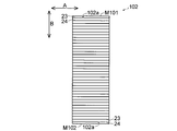
- FIG. 1st Embodiment of this invention It is a side view for demonstrating the structure of the positioning pin of the positioning stand used when manufacturing the solar cell module by 1st Embodiment of this invention. It is sectional drawing for demonstrating the manufacturing process of the solar cell module shown in FIG. It is sectional drawing for demonstrating the manufacturing process of the solar cell module shown in FIG. It is sectional drawing for demonstrating the manufacturing process of the solar cell module shown in FIG. It is sectional drawing for demonstrating the manufacturing process of the solar cell module shown in FIG. It is the bottom view which showed the structure of the back electrode type photovoltaic cell of the solar cell module by 2nd Embodiment of this invention. It is the bottom view which showed the structure of the back electrode type photovoltaic cell of the solar cell module by 2nd Embodiment of this invention.
- the solar cell module 1 includes a plurality of (for example, three) back electrode solar cells 2 and a plurality of back electrode solar cells 2 electrically.
- a flexible substrate 3 to be connected, a sealing material 4 covering the surface of the back electrode type solar cell 2, and a transparent substrate 5 disposed on the sealing material 4 are provided.
- the solar cell module 1 includes a sealing material and a back film (not shown) that cover the back side of the flexible substrate 3, a frame (not shown) that fixes the peripheral portions of the flexible substrate 3 and the transparent substrate 5, and the like. May be included.
- the flexible substrate 3 is an example of the “wiring substrate” in the present invention.
- the back electrode type solar cell 2 is formed in a substantially square shape (substantially rectangular shape) as shown in FIG. Further, as shown in FIG. 3, the back electrode type solar cell 2 includes a semiconductor substrate 20, an antireflection film 21 provided on the light receiving surface 20a of the semiconductor substrate 20, and a back surface (light receiving surface 20a) of the semiconductor substrate 20. A passivation layer 22, an n-electrode 23, and a p-electrode 24 provided on the surface 20b. The n electrode 23 and the p electrode 24 are examples of the “electrode” in the present invention.
- the semiconductor substrate 20 is formed using, for example, an n-type single crystal silicon substrate.
- the semiconductor substrate 20 includes an n-type conductive region 20c, an n-type diffusion region 20d provided on the back surface 20b side of the semiconductor substrate 20 and having an n-type impurity at a higher concentration than the n-type conductive region 20c, and the semiconductor substrate 20 And a p-type diffusion region 20e having a p-type impurity.
- Each of the n-type diffusion region 20d and the p-type diffusion region 20e is formed in a strip shape extending in the short side direction (A direction) of the back electrode type solar cell 2, for example. Further, the n-type diffusion regions 20d and the p-type diffusion regions 20e are alternately arranged in the B direction (a direction orthogonal to the A direction). In FIG. 3, two n-type diffusion regions 20d and two p-type diffusion regions 20e are shown. However, a large number (for example, several tens or more) of n-type diffusion regions 20d and p-type diffusion regions 20e are arranged. May be.
- the n-electrode 23 is in ohmic contact with the n-type diffusion region 20 d through the opening 22 a of the passivation layer 22.
- the p-electrode 24 is in ohmic contact with the p-type diffusion region 20 e through the opening 22 a of the passivation layer 22.
- each of the n electrode 23 and the p electrode 24 is formed in a strip shape extending in the A direction, for example.
- the n electrode 23 and the p electrode 24 have a predetermined line width (for example, about 0.12 mm), and are alternately arranged in the B direction at a predetermined pitch (for example, about 0.75 mm). If the pitch of n electrode 23 and p electrode 24 (n-type diffusion region 20d and p-type diffusion region 20e) is reduced, generally the power generation efficiency is improved.
- a plurality of (for example, two) through holes 2 a are formed in each of the back electrode type solar cells 2.
- the through hole 2a has an inner diameter (diameter) of about 1 mm, for example.
- the through hole 2a is an example of the “opening” and the “first positioning portion” in the present invention.
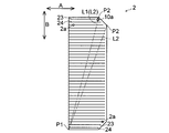
- the through hole 2a is formed in the vicinity of the edge of the back electrode type solar battery cell 2 as shown in FIG. Specifically, one through hole 2 a is formed in the vicinity of two opposing sides M 1 and M 2 of the back electrode type solar battery cell 2.
- the through hole 2a is preferably formed in a region within about 1 cm from the edge of the back electrode type solar cell 2.
- one through hole 2a is formed in each of the two regions S1 and S2 separated by the longest straight line L1 that crosses the back electrode type solar cell 2.
- the through-hole 2a is a back electrode type solar cell 2 that is divided by a straight line L2 that connects one vertex P1 of the back electrode type solar cell 2 and a vertex P2 arranged at a diagonal portion with respect to the vertex P1.
- One region is formed in each of the two regions S1 and S2.
- the two (one set) through-holes 2a are arranged at a distance greater than half the length of the longest straight line L1 that crosses the back electrode type solar battery cell 2. Further, the distance between the two (one set) through-holes 2 a is larger than the length of the shortest side M ⁇ b> 3 of the back electrode type solar cell 2.
- the through-hole 2a is arrange
- the through hole 2 a is formed on the n electrode 23 or the p electrode 24, but may be formed at a position different from the n electrode 23 and the p electrode 24. If comprised in this way, it can suppress that electric power generation efficiency falls.
- a part of the sealing material 4 may be filled in the through hole 2a.
- the back electrode type solar battery cell 2 is obtained by dividing (cutting) the substantially square solar battery wafer 10 shown in FIG. 7 into a plurality (for example, three) as shown in FIG. Is obtained.
- the dashed-two dotted line of FIG. 7 has shown the division position at the time of dividing
- an n electrode 23, a p electrode 24, a through hole 2a, and an alignment mark 10a are formed on the back surface side of the solar cell wafer 10.
- the n electrode 23 and the p electrode 24 are formed across the plurality of back electrode type solar cells 2.
- the n-electrode 23 and the p-electrode 24 are formed at a predetermined distance from the end in the A direction of the solar cell wafer 10, but may be formed up to the end in the A direction. .
- Alignment marks 10a are formed one by one at two corner portions of the solar cell wafer 10 that are positioned diagonally. Moreover, the alignment mark 10a functions as a reference position when forming the through hole 2a, as will be described later.
- the flexible substrate 3 (see FIG. 2) is formed of, for example, a polyimide substrate and can be bent (curved).
- the flexible substrate 3 is formed so that, for example, three back electrode type solar cells 2 are mounted.
- the dashed-two dotted line of FIG. 9 has shown the mounting area
- the flexible substrate 3 includes an insulating base material 30 and electrode layers 31 a, 31 b, 31 c, 31 d, 31 e made of a metal wiring layer formed on one surface of the base material 30, and 31f.
- the electrode layers 31a, 31b, 31c, 31d, 31e and 31f are respectively composed of the n-electrode 23 (see FIG. 4) of the back electrode solar cell 2c and the back electrode solar cell 2c.
- P electrode 24 (see FIG. 4), n electrode 23 of back electrode type solar cell 2d, p electrode 24 of back electrode type solar cell 2d, n electrode 23 of back electrode type solar cell 2e, and back electrode It is formed so as to correspond to the p electrode 24 of the solar cell 2e.
- electrode layer 31a, 31b, 31c, 31d, 31e and 31f are respectively the n electrode 23 of the back electrode type solar cell 2c, the p electrode 24 of the back electrode type solar cell 2c, and the back electrode type solar cell 2d.
- an insulating adhesive layer 6 is provided between the back electrode type solar cell 2 and the flexible substrate 3.
- the back electrode type solar battery cell 2 and the flexible substrate 3 are bonded by the adhesive layer 6. Further, a part of the adhesive layer 6 is filled in the through hole 2 a of the back electrode type solar cell 2 and the through hole 3 a of the flexible substrate 3.
- the adhesive layer 6 is an example of the “adhesive” in the present invention.
- each of the electrode layers 31a to 31f is formed in a comb shape in which a plurality of comb teeth extending in the A direction are connected at the end portions in the A direction.
- the electrode layer 31b and the electrode layer 31c are electrically connected via a plurality of connection portions 31g, and the electrode layer 31d and the electrode layer 31e are electrically connected via a plurality of connection portions 31h. It is connected to the. Thereby, the three back electrode type photovoltaic cells 2 are connected in series.
- the end portions in the A direction of the electrode layers 31a to 31f are arranged to the outside of the mounting region T on which the back electrode type solar cells 2 are mounted. If an insulating layer (not shown) is provided on the end portions in the A direction of the electrode layers 31a to 31f, the electrode layers 31a to 31f can be accommodated inside the mounting region T of the back electrode type solar cell 2. It is also possible to form it. In this case, it is possible to improve the mounting density of the back electrode type solar cells 2.
- the flexible substrate 3 is formed with a through hole 3 a at a position corresponding to the through hole 2 a of the back electrode type solar cell 2. That is, as shown in FIG. 1, in a state where the back electrode type solar cell 2 is mounted on the flexible substrate 3, the through hole 2 a of the back electrode type solar cell 2 and the through hole 3 a of the flexible substrate 3 have a thickness. It is arranged to overlap in the direction.
- the through hole 3a has the same inner diameter (diameter) as the through hole 2a of the back electrode type solar cell 2 (for example, about 1 mm).
- the through hole 3a is an example of the “opening” and the “second positioning portion” in the present invention.
- the sealing material 4 is formed using, for example, a resin transparent to sunlight. Moreover, the sealing material 4 may be formed with polyolefin resin or other resin.
- the transparent substrate 5 is formed using, for example, a PC (polycarbonate resin) or a glass substrate that is transparent to sunlight, but is not particularly limited as long as it is transparent to sunlight.
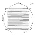
- a substantially square solar cell wafer 10 is prepared. Specifically, the substantially square solar cell wafer 10 is cut out by dividing (cutting) the substantially circular solar cell wafer 10b (see FIG. 11) at the dividing position C1 (two-dot chain line in FIG. 11). It is.
- the substantially circular solar cell wafer 10b can be manufactured using a general wafer manufacturing process, and includes an n-type diffusion region 20d, a p-type diffusion region 20e, an antireflection film 21, a passivation layer 22, The n electrode 23, the p electrode 24, and the alignment mark 10a are formed.
- this solar cell wafer 10b (10) is normally used without being divided into a plurality of back electrode type solar cells 2.
- the through-hole 2a is divided into two regions S1 and S2 (FIG. 4) separated by the longest straight line L1 (see FIG. 4) that crosses the back electrode type solar battery cell 2.
- the through-hole 2a is defined by a straight line L2 connecting one vertex P1 (see FIG. 4) of the back electrode type solar cell 2 and a vertex P2 (see FIG. 4) arranged at a diagonal portion with respect to the vertex P1.
- One is formed in each of the two regions S1 and S2 of the separated back electrode type solar cell 2.
- the through-hole 2a is formed in the vicinity of the two sides M1 and M2 (refer FIG. 4) which the back surface electrode type photovoltaic cell 2 opposes one by one. Further, the distance between the two (one set) of through holes 2 a is set to be longer than the length of the shortest side M ⁇ b> 3 of the back electrode type solar cell 2.
- a through hole 3 a is formed at a position of the flexible substrate 3 corresponding to the through hole 2 a of the back electrode type solar cell 2.
- the flexible substrate 3 is arrange
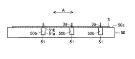
- the positioning pin 51 is an example of the “positioning member” in the present invention.
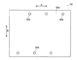
- the positioning table 50 includes a placement surface 50a on which the flexible substrate 3 is disposed, and a plurality of insertion holes 50b formed in the placement surface 50a.
- the insertion portion 51a of the positioning pin 51 (see FIG. 15) is inserted into the insertion hole 50b.
- the pin portion 51b of the positioning pin 51 has a diameter (for example, a diameter of about 0.8 mm) that is slightly smaller than the inner diameters of the through holes 2a and 3a.
- tip (upper end) of the pin part 51b may be formed in the taper shape.
- the adhesive layer 6 having a predetermined thickness is disposed (applied) in the mounting region T (see FIG. 9) of the flexible substrate 3. At this time, the adhesive layer 6 is disposed in a region other than the peripheral portion of the mounting region T and a region other than the vicinity of the positioning pin 51.
- the back surface electrode type photovoltaic cell 2 is arrange
- the through hole 2 a is disposed so as to overlap the through hole 3 a of the flexible substrate 3.
- the adhesive layer 6 is heated and semi-cured. Thereby, the back electrode type solar cell 2 is bonded to the flexible substrate 3 via the adhesive layer 6.
- the adhesive layer 6 spreads outward from the central portion of the back electrode solar cell 2 and flows into the recess between the n electrode 23 and the p electrode 24 of the back electrode solar cell 2.
- the adhesive layer 6 is disposed in a region other than the peripheral portion of the mounting region T and a region other than the vicinity of the positioning pin 51, the adhesive layer 6 is provided in the back electrode type solar cell. 2 (mounting area T) can be prevented from sticking to the positioning table 50 or from the positioning pin 51. Thereby, it is possible to suppress the occurrence of a work loss for cleaning the positioning table 50 (positioning pin 51).
- the sealing material 4 and the transparent substrate 5 are disposed on the back electrode type solar cell 2 and the flexible substrate 3, and the transparent substrate 5 is added downward (to the flexible substrate 3 side).
- the sealing material 4 is heated and cured while pressing.
- the back electrode type solar cell 2 is electrically connected to the flexible substrate 3.
- the adhesive layer 6 is filled in the through hole 2a of the back electrode type solar cell 2 and the through hole 3a of the flexible substrate 3 and is fully cured.
- the solar cell module 1 according to the first embodiment of the present invention shown in FIG. 1 is manufactured.
- the contact bonding layer 6 is heated, pressing the back surface electrode type solar cell 2 downward (positioning stand 50 side). You may make it harden.
- the positioning table 50 may be configured such that the positioning pin 51 moves downward when the back electrode type solar battery cell 2 is pressed downward.
- a spring (not shown) may be disposed in the insertion hole 50b of the positioning table 50 so that the positioning pin 51 moves downward when a force is applied downward to the positioning pin 51.
- a recess for avoiding contact with the positioning pin 51 may be provided on a pressing surface (lower surface) of a member (not shown) that pressurizes the back electrode type solar cell 2 downward.
- the back electrode type solar battery cell 2 can be positioned by the through hole 2a.
- special apparatuses such as an infrared irradiation apparatus and an infrared imaging device, in order to position the back electrode type photovoltaic cell 2, manufacturing cost can be reduced.
- the step of manufacturing the substantially circular solar cell wafer 10b (the step of manufacturing the n-type diffusion region 20d, the p-type diffusion region 20e, the n electrode 23, the p electrode 24, and the like). ), It is not necessary to determine the shape of the back electrode type solar cell 2 and the position of the through hole 2a. That is, after manufacturing the substantially circular solar cell wafer 10b, the shape of the back electrode solar cell 2 can be determined, and the through hole 2a can be formed in accordance with the shape of the back electrode solar cell 2. . Thereby, the design freedom of the back electrode type solar cell 2 can be improved.
- the types of solar cell wafers 10 are increased. Can be suppressed.
- the positioning accuracy of the back electrode type solar battery cell 2 is easily improved. be able to.
- the two (one set) of through holes 2a are separated by a distance larger than half the length of the longest straight line L1 that crosses the back electrode type solar battery cell 2. Deploy. Thereby, since the distance between the through-holes 2a can be enlarged, the positioning accuracy of the back surface electrode type solar battery cell 2 can be improved more easily.
- the through hole 2a is formed in the vicinity of the edge of the back electrode type solar battery cell 2.
- the through hole 2a divides the n electrode 23 or the p electrode 24, the portion outside the through hole 2a does not contribute to power generation.
- the through-hole 2a is formed in the edge part vicinity of the back electrode type photovoltaic cell 2 as mentioned above, the part which does not contribute to electric power generation can be made small. For this reason, as described above, it is particularly effective to form the through hole 2a in the vicinity of the edge of the back electrode type solar battery cell 2.
- the through hole 2 a is formed in accordance with the shape of the back electrode type solar battery cell 2 after manufacturing the substantially circular solar battery wafer 10 b. Can be easily formed, and the back electrode type solar battery cell 2 can be easily divided (cut out) into a desired shape.
- the adhesive layer 6 is filled into the through hole 2 a of the back electrode type solar cell 2 and the through hole 3 a of the flexible substrate 3.
- the adhesive strength of the back electrode type solar cell 2 and the flexible substrate 3 can be improved.
- it can suppress that a water
- the flexible substrate 3 is arranged so that the through hole 3 a engages the positioning pin 51, and the back surface electrode so that the through hole 2 a engages the positioning pin 51. Since the flexible substrate 3 and the back electrode solar cell 2 can be easily positioned by arranging the solar cell 2, the back electrode solar cell 2 can be easily attached to the flexible substrate 3. Can do.
- each of the back electrode type solar cells 102 is formed with a plurality of (for example, two) cutout portions 102a. Yes.
- the notch 102 a is formed at the edge of the back electrode solar cell 102.
- the notch 102 a is formed in a portion different from the n electrode 23 and the p electrode 24. That is, the notch 102 a is formed at a predetermined distance from the n electrode 23 and the p electrode 24.
- the notch 102a is an example of the “opening” and the “first positioning portion” in the present invention.
- the notch portion 102a is formed one by one on two opposing sides M101 and M102 of the back electrode type solar cell 102.
- the back electrode type solar battery cell 102 is obtained by dividing the substantially square solar battery wafer 110 shown in FIG. 22 into a plurality (for example, three). Note that a two-dot chain line in FIG. 22 indicates a division position when dividing the plurality of back electrode type solar cells 102.
- the notch 102a may be formed by forming a through hole on a division position of a substantially circular solar cell wafer (not shown) and dividing the through hole.
- the cutout portion 102a may be formed after the solar cell wafer 110 having a substantially square shape is formed.
- the notch portion 102a is formed in a portion different from the n electrode 23 and the p electrode 24, thereby suppressing the power generation efficiency of the back electrode type solar battery cell 102 from being lowered. can do.
- the notch portion 102a is formed so that the positioning portion (notch portion 102a) is different from the n electrode 23 and the p electrode 24. It can be easily formed on the part.
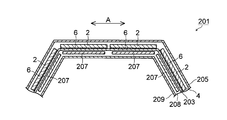
- the solar cell module 201 includes a plurality of (for example, three or more) back electrode type solar cells 2 and a plurality of back electrode type solar cells 2 electrically.
- a flexible substrate 203 connected to the substrate, a sealing material 4 covering the surface of the back electrode type solar cell 2, a transparent sheet 205 disposed on the sealing material 4, and a back surface of the flexible substrate 203.
- a plurality of reinforcing plates 207, a sealing material 208 that covers the back surface side of the flexible substrate 203 and the reinforcing plate 207, and a back film 209 disposed on the back surface of the sealing material 208 are provided.
- the flexible substrate 203 is an example of the “wiring substrate” in the present invention.
- the flexible substrate 203 is formed so that, for example, four (three or more) back electrode type solar cells 2 are mounted.
- the transparent sheet 205 is made of, for example, a sheet material that is transparent to sunlight and can be bent (curved).
- the transparent sheet 205 is formed of a fluorine-based sheet.
- the solar cell module 201 can be bent at a position between the back electrode type solar cells 2. It is. Thereby, the freedom degree of the usage pattern of the solar cell module 201 can be improved.
- the reinforcing plate 207 is formed of a metal thin plate made of, for example, stainless steel. Further, the reinforcing plate 207 is disposed at a position directly below (directly behind) the back electrode type solar battery cell 2 and is provided for each back electrode type solar battery cell 2. Thereby, it is possible to suppress that the back electrode type solar cell 2 is broken. That is, it is possible to bend and use the solar cell module 201 while suppressing the back electrode type solar cell 2 from cracking.
- the sealing material 208 may be formed using the same resin as the sealing material 4. Further, unlike the sealing material 4, the sealing material 208 may be formed using, for example, a resin that is not transparent to sunlight.
- a sheet material made of a weather resistant film can be used.
- an n-type silicon substrate is used.
- the present invention is not limited to this, and a p-type silicon substrate may be used, or a semiconductor substrate other than a silicon substrate may be used. Also good.
- first positioning portions may be provided in the solar cell.
- one first positioning part may be provided in one back electrode type solar cell, and in this case, the shape of the first positioning part is set to a shape other than a circular shape such as a rectangular shape or a cross shape. Also good.
- back electrode type photovoltaic cell was shown about the example formed in substantially square shape (rectangular shape), this invention is not limited to this, A back electrode type photovoltaic cell is substantially triangular shape. It can be formed in any other shape.
- the through-hole is formed in the substantially circular solar cell wafer. Also good.
- an alignment mark 310a may be provided on the outer side of the back electrode type solar cell 2 (outside of the division position C301) like the solar cell wafer 310b according to the first modification of the present invention shown in FIG. .
- the solar cell module by the 2nd modification of this invention shown in FIG. Like 401, you may mount the back electrode type photovoltaic cell 2 in the circuit mounting board
- a back electrode type An ACF (Anisotropic Conductive Film) or ACP (Anisotropic Conductive Paste) is disposed between the solar cell and the flexible substrate (wiring substrate) to form a back electrode type solar cell.
- the cell and the flexible substrate may be electrically connected via ACF or ACP.
- ACF or ACP may not be filled in the through hole of the back electrode type solar cell and the through hole of the flexible substrate.
- the back electrode type solar cell and the flexible substrate may be electrically connected by pressure contact without disposing the adhesive layer, ACF and ACP between the back electrode type solar cell and the flexible substrate. That is, the back electrode type solar cell is directly arranged on the flexible substrate, and the sealing material and the transparent substrate are arranged on the back electrode type solar cell. Then, by pressing the transparent substrate downward, the back electrode solar cell is pressed downward (flexible substrate side), and the n electrode and the p electrode of the back electrode solar cell are applied to the electrode layer of the flexible substrate. You may make it contact. In this case, the n electrode and the p electrode of the back electrode type solar battery cell and the electrode layer of the flexible substrate can be more reliably brought into contact with each other.
- a power supply circuit A circuit mounting board (wiring board) made of a glass epoxy board or the like on which (circuit components) is mounted may be arranged to electrically connect the flexible board and the circuit mounting board.
- the solar cell module functions as a stabilized power source having added value (power supply circuit), and the entire solar cell module (or a solar cell system including the solar cell module) can be downsized. .
- a recessed part is provided in a back electrode type photovoltaic cell. (A hole that does not penetrate) may be provided. In this case, the length of the pin portion of the positioning pin may be reduced.
- a through hole is provided in a flexible substrate (wiring substrate)
- wiring substrate wiring substrate
- the present invention is not limited to this, and a notch portion may be provided in the wiring substrate.
- the said embodiment showed about the example which has arrange
- this invention is not limited to this.
- the wiring board may be arranged on the back electrode type solar cell. In this case, if the thickness of the wiring board is equal to or greater than a predetermined value, the wiring board may be provided with a recess (a hole not penetrating).
- the inner diameter (diameter) of the through hole of the back electrode type solar cell and the through hole of the flexible substrate is about 1 mm, and the diameter of the pin portion of the positioning pin is about 0.8 mm.
- the inner diameters of the through hole of the back electrode type solar cell and the through hole of the flexible substrate may be made larger than about 1 mm.
Landscapes
- Photovoltaic Devices (AREA)
Abstract
太陽電池ウェハの種類が多くなるのを抑制しながら、低コストな裏面電極型太陽電池モジュールを得ることが可能な裏面電極型太陽電池セルを提供する。この裏面電極型太陽電池セル(2)は、太陽電池ウェハ(10)を分割することにより形成されているとともに、裏面(20b)上にn電極(23)およびp電極(24)が設けられ、かつ、貫通穴(2a)が形成されている。
Description
この発明は、裏面電極型太陽電池セル、太陽電池モジュール、太陽電池ウェハおよび太陽電池モジュールの製造方法に関し、特に、受光面とは反対側の面に異なる極性の電極が設けられた裏面電極型太陽電池セル、太陽電池モジュール、太陽電池ウェハおよび太陽電池モジュールの製造方法に関する。
従来、受光面とは反対側の面(裏面)に異なる極性の電極が設けられた裏面電極型太陽電池が知られている。この裏面電極型太陽電池では、受光面側に電極を設けないので、太陽電池の受光面積が小さくなることがなく、発電効率を向上させることが可能である。
しかしながら、裏面電極型太陽電池は、裏面に電極が設けられているので、裏面電極型太陽電池を配線基板に取り付ける際の裏面電極型太陽電池と配線基板との位置合わせが困難であるという不都合がある。
そこで、上記不都合を改善することが可能な方法が提案されている(例えば、特許文献1参照)。上記特許文献1には、裏面電極型太陽電池セル(太陽電池ウェハ)にセルアライメントマークを形成するとともに、配線フィルム(配線基板)に配線フィルムアライメントマークを形成し、裏面電極型太陽電池セルと配線フィルムとの位置合わせを行う裏面電極型太陽電池セルの裏面パターン観察方法が開示されている。そして、上記特許文献1では、裏面電極型太陽電池セルの受光面側から赤外線を照射して、裏面電極型太陽電池セルのセルアライメントマークと配線フィルムの配線フィルムアライメントマークとを認識することにより、裏面電極型太陽電池セルと配線フィルムとの位置合わせを行い、裏面電極型太陽電池セルを配線フィルムに電気的に接続させる。
一方、複雑な形状の領域に効率よく太陽電池を配置したい場合や、大電流は必要としないが小さい面積で比較的高い電圧が要求される携帯機器などに太陽電池を用いる場合などに、太陽電池ウェハを所定の形状の裏面電極型太陽電池セルに分割し、裏面電極型太陽電池セルを配線基板に電気的に接続する方法も知られている。
このように、太陽電池ウェハを複数の裏面電極型太陽電池セルに分割し配線基板に取り付ける場合、裏面電極型太陽電池セル毎にアライメントマークを形成しておけば、裏面電極型太陽電池セルと配線基板との位置合わせを行うことが可能である。
しかしながら、上記特許文献1では、裏面電極型太陽電池セル(太陽電池ウェハ)のセルアライメントマークと配線フィルムの配線フィルムアライメントマークとを認識するために、赤外線を照射する赤外線照射装置や赤外線を撮像する赤外線撮像装置などの特別な装置が必要であるという問題点がある。
また、太陽電池ウェハを複数の裏面電極型太陽電池セルに分割し配線基板に取り付ける場合、裏面電極型太陽電池セル毎にアライメントマークが必要であるが、略円形状の太陽電池ウェハを製造する段階(不純物領域や電極などを製造する段階)で、裏面電極型太陽電池セルの形状およびアライメントマークの位置を決定しておく必要があるという問題点がある。
また、太陽電池ウェハを複数の裏面電極型太陽電池セルに分割する場合と分割しない場合とで異なる太陽電池ウェハを製造する必要があり、太陽電池ウェハの種類が多くなるという問題点もある。
この発明は、上記のような課題を解決するためになされたものであり、この発明の目的は、太陽電池ウェハの種類が多くなるのを抑制しながら、低コストな裏面電極型太陽電池モジュールを得ることが可能な裏面電極型太陽電池セル、太陽電池モジュール、太陽電池ウェハおよび太陽電池モジュールの製造方法を提供することである。
上記目的を達成するために、この発明の第1の局面による裏面電極型太陽電池セルは、受光面とは反対側の面に異なる極性の電極が設けられた裏面電極型太陽電池セルであって、受光面とは反対側の面に異なる極性の電極が設けられた太陽電池ウェハを切断することにより形成されているとともに、開口部または凹部からなる第1位置決め部が形成されている。
第1の局面による裏面電極型太陽電池セルでは、上記のように、開口部または凹部からなる第1位置決め部を形成することによって、第1位置決め部により裏面電極型太陽電池セルを位置決めすることができる。これにより、裏面電極型太陽電池セルを位置決めするために、例えば赤外線照射装置や赤外線撮像装置などの特別な装置を用いる必要がないので、製造コストを低減できる。また、第1位置決め部に係合する位置決めピンなどを用いるだけで、容易に、裏面電極型太陽電池セルを位置決めすることができる。
また、第1の局面による裏面電極型太陽電池セルでは、略円形状の太陽電池ウェハを製造する段階(不純物領域や電極などを製造する段階)において、裏面電極型太陽電池セルの形状および第1位置決め部の位置を決定しておく必要がない。すなわち、略円形状の太陽電池ウェハを製造した後で、裏面電極型太陽電池セルの形状を決定し、裏面電極型太陽電池セルの形状に合わせて第1位置決め部を形成することができる。これにより、裏面電極型太陽電池セルの設計自由度を向上させることができる。
また、太陽電池ウェハを複数の裏面電極型太陽電池セルに分割する場合と分割しない場合とで異なる太陽電池ウェハを製造する必要がないので、太陽電池ウェハの種類が多くなるのを抑制することができる。
上記第1の局面による裏面電極型太陽電池セルにおいて、好ましくは、第1位置決め部は、少なくとも2つ形成されている。このように構成すれば、裏面電極型太陽電池セルの位置決め精度を、容易に向上させることができる。
上記第1位置決め部が少なくとも2つ形成されている裏面電極型太陽電池セルにおいて、好ましくは、第1位置決め部のうちの少なくとも2つは、裏面電極型太陽電池セルを横切る最も長い直線の長さの半分よりも大きい距離を隔てて配置されている。このように構成すれば、第1位置決め部同士の距離を大きくすることができるので、裏面電極型太陽電池セルの位置決め精度を、容易に、より向上させることができる。
上記第1位置決め部が少なくとも2つ形成されている裏面電極型太陽電池セルにおいて、好ましくは、第1位置決め部のうちの少なくとも1つは、裏面電極型太陽電池セルの縁部または縁部近傍に形成されている。このように、裏面電極型太陽電池セルの、比較的発電効率の低い縁部または縁部近傍に、第1位置決め部を形成することによって、第1位置決め部を設けることによる発電効率の低下を、抑制することができる。
上記第1の局面による裏面電極型太陽電池セルにおいて、好ましくは、第1位置決め部は、電極とは異なる部分に形成されている。このように構成すれば、裏面電極型太陽電池セルの発電効率が低下するのを抑制することができる。
この発明の第2の局面による太陽電池モジュールは、上記の構成の裏面電極型太陽電池セルと、裏面電極型太陽電池セルが取り付けられる配線基板とを備え、裏面電極型太陽電池セルには、開口部または凹部からなる第1位置決め部が形成されており、配線基板には、開口部または凹部からなる第2位置決め部が形成されており、裏面電極型太陽電池セルは、第1位置決め部が第2位置決め部に重なるように、配線基板上に配置されている。このように構成すれば、太陽電池ウェハの種類が多くなるのを抑制しながら、低コストな太陽電池モジュールを得ることができる。
また、配線基板に、開口部または凹部からなる第2位置決め部を形成することによって、第2位置決め部により配線基板を位置決めすることができる。そして、第1位置決め部および第2位置決め部により、裏面電極型太陽電池セルと配線基板とを容易に位置合わせすることができる。
上記第2の局面による太陽電池モジュールにおいて、好ましくは、第1位置決め部および第2位置決め部には、絶縁性の接着材が充填されている。このように構成すれば、裏面電極型太陽電池セルと配線基板との間の接着強度を向上させることができる。また、第1位置決め部および第2位置決め部に水分が浸入するのを抑制することができ、信頼性が低下するのを抑制することができる。
上記第2の局面による太陽電池モジュールにおいて、好ましくは、配線基板は、回路部品が取り付けられた回路実装基板を含む。このように構成すれば、裏面電極型太陽電池セルからの出力を回路実装基板に直接供給することができ、太陽電池モジュール(または太陽電池モジュールを含む太陽電池システム)全体を小型化することができる。
この発明の第3の局面による太陽電池ウェハは、受光面とは反対側の面に異なる極性の電極が設けられ、複数の裏面電極型太陽電池セルに分割される太陽電池ウェハであって、裏面電極型太陽電池セル毎に、開口部または凹部からなる第1位置決め部が形成されている。
第3の局面による太陽電池ウェハでは、上記のように、裏面電極型太陽電池セル毎に、開口部または凹部からなる第1位置決め部を形成することによって、第1位置決め部により裏面電極型太陽電池セルを位置決めすることができる。これにより、裏面電極型太陽電池セルを位置決めするために、例えば赤外線照射装置や赤外線撮像装置などの特別な装置を用いる必要がないので、製造コストを低減できる。また、第1位置決め部に係合する位置決めピンなどを用いるだけで、容易に、裏面電極型太陽電池セルを位置決めすることができる。
また、第3の局面による太陽電池ウェハでは、略円形状の太陽電池ウェハを製造する段階(不純物領域や電極などを製造する段階)において、裏面電極型太陽電池セルの形状および第1位置決め部の位置を決定しておく必要がない。すなわち、略円形状の太陽電池ウェハを製造した後で、裏面電極型太陽電池セルの形状を決定し、裏面電極型太陽電池セルの形状に合わせて第1位置決め部を形成することができる。これにより、裏面電極型太陽電池セルの設計自由度を向上させることができる。
また、太陽電池ウェハを複数の裏面電極型太陽電池セルに分割する場合と分割しない場合とで異なる太陽電池ウェハを製造する必要がないので、太陽電池ウェハの種類が多くなるのを抑制することができる。
上記第3の局面による太陽電池ウェハにおいて、電極は、複数の裏面電極型太陽電池セルに跨って形成されていてもよい。
上記第3の局面による太陽電池ウェハにおいて、好ましくは、第1位置決め部を形成するためのアライメントマークが形成されている。このように構成すれば、略円形状の太陽電池ウェハを製造した後で、裏面電極型太陽電池セルの形状に合わせて第1位置決め部を、容易に形成することができるとともに、裏面電極型太陽電池セルを、容易に所望の形状に分割することができる。
この発明の第4の局面による太陽電池モジュールの製造方法は、受光面とは反対側の面に異なる極性の電極が設けられ、1つ以上の裏面電極型太陽電池セルを含む太陽電池ウェハを準備する工程と、裏面電極型太陽電池セル毎に、開口部または凹部からなる第1位置決め部を形成する工程と、太陽電池ウェハを切断することにより、裏面電極型太陽電池セルを切り出す工程と、開口部または凹部からなる第2位置決め部が形成された配線基板を準備する工程と、裏面電極型太陽電池セルを、第1位置決め部が第2位置決め部に重なるように、配線基板上に配置する工程と、裏面電極型太陽電池セルを、配線基板に取り付ける工程とを備える。
第4の局面による太陽電池モジュールの製造方法では、上記のように、裏面電極型太陽電池セル毎に、開口部または凹部からなる第1位置決め部を形成することによって、第1位置決め部により裏面電極型太陽電池セルを位置決めすることができる。これにより、裏面電極型太陽電池セルを位置決めするために、例えば赤外線照射装置や赤外線撮像装置などの特別な装置を用いる必要がないので、製造コストを低減できる。また、第1位置決め部および第2位置決め部に係合する位置決めピンなどを用いるだけで、容易に、裏面電極型太陽電池セルおよび配線基板を位置決めすることができる。
また、第4の局面による太陽電池モジュールの製造方法では、略円形状の太陽電池ウェハを製造する段階(不純物領域や電極などを製造する段階)において、裏面電極型太陽電池セルの形状および第1位置決め部の位置を決定しておく必要がない。すなわち、略円形状の太陽電池ウェハを製造した後で、裏面電極型太陽電池セルの形状を決定し、裏面電極型太陽電池セルの形状に合わせて第1位置決め部を形成することができる。これにより、裏面電極型太陽電池セルの設計自由度を向上させることができる。
また、太陽電池ウェハを複数の裏面電極型太陽電池セルに分割する場合と分割しない場合とで異なる太陽電池ウェハを製造する必要がないので、太陽電池ウェハの種類が多くなるのを抑制することができる。
上記第4の局面による太陽電池モジュールの製造方法において、好ましくは、裏面電極型太陽電池セル毎に、第1位置決め部を形成する工程は、裏面電極型太陽電池セル毎に、第1位置決め部を少なくとも2つ形成する工程を含む。このように構成すれば、裏面電極型太陽電池セルの位置決め精度を、容易に向上させることができる。
上記第4の局面による太陽電池モジュールの製造方法において、好ましくは、裏面電極型太陽電池セルを、配線基板上に配置する工程は、第2位置決め部が位置決め部材に係合するように、配線基板を配置する工程と、第1位置決め部が位置決め部材に係合するように、裏面電極型太陽電池セルを配置する工程とを含む。このように構成すれば、配線基板および裏面電極型太陽電池セルを、容易に位置決めすることができるので、裏面電極型太陽電池セルを、配線基板に容易に取り付けることができる。
上記第4の局面による太陽電池モジュールの製造方法において、好ましくは、太陽電池ウェハを準備する工程は、アライメントマークが形成されている太陽電池ウェハを準備する工程を含み、裏面電極型太陽電池セル毎に、第1位置決め部を形成する工程は、アライメントマークを基準として、裏面電極型太陽電池セル毎に、第1位置決め部を形成する工程を含む。このように構成すれば、略円形状の太陽電池ウェハを製造した後で、裏面電極型太陽電池セルの形状に合わせて第1位置決め部を、容易に形成することができるとともに、裏面電極型太陽電池セルを、容易に所望の形状に分割することができる。
以上のように、本発明によれば、太陽電池ウェハの種類が多くなるのを抑制しながら、低コストな裏面電極型太陽電池モジュールを得ることが可能な太陽電池ウェハおよびそれを備えた太陽電池モジュールを容易に得ることができる。
以下、本発明の実施形態について図面を参照して説明する。なお、理解を容易にするために、断面図であってもハッチングを施さない場合がある。
(第1実施形態)
まず、図1~図9を参照して、本発明の第1実施形態による太陽電池モジュール1の構造について説明する。
まず、図1~図9を参照して、本発明の第1実施形態による太陽電池モジュール1の構造について説明する。
本発明の第1実施形態による太陽電池モジュール1は、図1に示すように、複数(例えば3つ)の裏面電極型太陽電池セル2と、複数の裏面電極型太陽電池セル2が電気的に接続されるフレキシブル基板3と、裏面電極型太陽電池セル2の表面を覆う封止材4と、封止材4上に配置された透明基板5とを備えている。なお、裏面電極型太陽電池セル2は、1つの太陽電池モジュール1において、1つ、2つまたは4つ以上設けられていてもよい。また、太陽電池モジュール1は、フレキシブル基板3の裏面側を覆う封止材および裏面フィルム(図示せず)や、フレキシブル基板3および透明基板5の周縁部を固定する枠体(図示せず)などを含んでいてもよい。また、フレキシブル基板3は、本発明の「配線基板」の一例である。
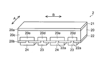
裏面電極型太陽電池セル2は、図2に示すように、略四角形状(略長方形状)に形成されている。また、裏面電極型太陽電池セル2は、図3に示すように、半導体基板20と、半導体基板20の受光面20a上に設けられた反射防止膜21と、半導体基板20の裏面(受光面20aとは反対側の面)20b上に設けられたパッシベーション層22、n電極23およびp電極24とを含んでいる。なお、n電極23およびp電極24は、本発明の「電極」の一例である。
半導体基板20は、例えば、n型の単結晶シリコン基板を用いて形成されている。また、半導体基板20は、n型導電領域20cと、半導体基板20の裏面20b側に設けられ、n型導電領域20cよりも高濃度のn型不純物を有するn型拡散領域20dと、半導体基板20の裏面20b側に設けられ、p型不純物を有するp型拡散領域20eとを含んでいる。
n型拡散領域20dおよびp型拡散領域20eの各々は、裏面電極型太陽電池セル2の例えば短手方向(A方向)に延びる帯状に形成されている。また、n型拡散領域20dおよびp型拡散領域20eは、B方向(A方向と直交する方向)に交互に配置されている。なお、図3では、n型拡散領域20dおよびp型拡散領域20eを、2つずつ示したが、n型拡散領域20dおよびp型拡散領域20eは、多数(例えば数十個以上)配置されていてもよい。
n電極23は、パッシベーション層22の開口部22aを介して、n型拡散領域20dにオーミック接触されている。同様に、p電極24は、パッシベーション層22の開口部22aを介して、p型拡散領域20eにオーミック接触されている。
また、n電極23およびp電極24の各々は、例えばA方向に延びる帯状に形成されている。また、n電極23およびp電極24は、所定の線幅(例えば、約0.12mm)を有するとともに、B方向に交互に、所定のピッチ(例えば、約0.75mm)で配置されている。なお、n電極23およびp電極24(n型拡散領域20dおよびp型拡散領域20e)のピッチを小さくすると、一般的に発電効率が向上する。
ここで、第1実施形態では、図1および図2に示すように、裏面電極型太陽電池セル2の各々には、複数(例えば2つ)の貫通穴2aが形成されている。この貫通穴2aは、例えば、約1mmの内径(直径)を有する。なお、貫通穴2aは、本発明の「開口部」および「第1位置決め部」の一例である。
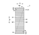
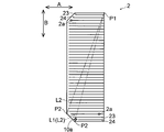
第1実施形態では、貫通穴2aは、図4に示すように、裏面電極型太陽電池セル2の縁部近傍に形成されている。具体的には、貫通穴2aは、裏面電極型太陽電池セル2の対向する2つの辺M1およびM2の近傍に、1つずつ形成されている。なお、貫通穴2aは、裏面電極型太陽電池セル2の縁部から約1cm以内の領域に形成されていることが好ましい。
第1実施形態では、貫通穴2aは、裏面電極型太陽電池セル2を横切る最も長い直線L1により区分けされた2つの領域S1およびS2の各々に、1つ形成されている。言い換えると、貫通穴2aは、裏面電極型太陽電池セル2の1つの頂点P1と、頂点P1に対する対角部分に配置される頂点P2とを結ぶ直線L2により区分けされた裏面電極型太陽電池セル2の2つの領域S1およびS2の各々に、1つ形成されている。
また、第1実施形態では、2つ(1組)の貫通穴2aは、裏面電極型太陽電池セル2を横切る最も長い直線L1の長さの半分よりも大きい距離を隔てて配置されている。また、2つ(1組)の貫通穴2aの間の距離は、裏面電極型太陽電池セル2の最も短い辺M3の長さよりも大きい。
なお、図5および図6に示すように、コーナー部が切り取られた形状の裏面電極型太陽電池セル2においても、貫通穴2aは、同様の位置に配置されている。
また、図4では、貫通穴2aは、n電極23またはp電極24上に形成されているが、n電極23およびp電極24とは異なる位置に形成されていてもよい。このように構成すれば、発電効率が低下するのを抑制することが可能である。
また、貫通穴2aには、図1に示すように、封止材4の一部が充填されていてもよい。
また、裏面電極型太陽電池セル2は、後述するように、図7に示した略正方形状の太陽電池ウェハ10を、図8に示すように複数(例えば3つ)に分割(切断)することにより得られる。なお、図7の2点鎖線は、複数の裏面電極型太陽電池セル2に分割する際の分割位置を示している。
また、図7に示すように、太陽電池ウェハ10の裏面側には、n電極23、p電極24、貫通穴2aおよびアライメントマーク10aが形成されている。
また、裏面電極型太陽電池セル2に分割される前の状態(図7の状態)では、n電極23およびp電極24は、複数の裏面電極型太陽電池セル2に跨って形成されている。なお、図7では、n電極23およびp電極24は、太陽電池ウェハ10のA方向の端部から所定の距離を隔てて形成されているが、A方向の端部まで形成されていてもよい。
アライメントマーク10aは、太陽電池ウェハ10のうちの、対角に位置する2つのコーナー部に、1つずつ形成されている。また、アライメントマーク10aは、後述するように、貫通穴2aを形成する際の基準位置として機能する。
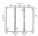
フレキシブル基板3(図2参照)は、例えばポリイミド基板などにより形成されており、屈曲(湾曲)可能である。また、フレキシブル基板3は、図2および図9に示すように、例えば3つの裏面電極型太陽電池セル2が搭載されるように形成されている。なお、図9の2点鎖線は、裏面電極型太陽電池セル2が搭載される搭載領域Tを示している。
また、フレキシブル基板3は、図9に示すように、絶縁性の基材30と、基材30の一方面上に形成された金属配線層からなる電極層31a、31b、31c、31d、31eおよび31fとを含んでいる。
また、図2に示すように、電極層31a、31b、31c、31d、31eおよび31fは、それぞれ、裏面電極型太陽電池セル2cのn電極23(図4参照)、裏面電極型太陽電池セル2cのp電極24(図4参照)、裏面電極型太陽電池セル2dのn電極23、裏面電極型太陽電池セル2dのp電極24、裏面電極型太陽電池セル2eのn電極23、および、裏面電極型太陽電池セル2eのp電極24に対応するように形成されている。そして、電極層31a、31b、31c、31d、31eおよび31fは、それぞれ、裏面電極型太陽電池セル2cのn電極23、裏面電極型太陽電池セル2cのp電極24、裏面電極型太陽電池セル2dのn電極23、裏面電極型太陽電池セル2dのp電極24、裏面電極型太陽電池セル2eのn電極23、および、裏面電極型太陽電池セル2eのp電極24に電気的に接続されている。
また、第1実施形態では、図1に示すように、裏面電極型太陽電池セル2とフレキシブル基板3との間には、絶縁性の接着層6が設けられている。そして、接着層6により、裏面電極型太陽電池セル2とフレキシブル基板3とが接着されている。また、接着層6の一部は、裏面電極型太陽電池セル2の貫通穴2aおよびフレキシブル基板3の貫通穴3aに充填されている。なお、接着層6は、本発明の「接着材」の一例である。
また、図9に示すように、電極層31a~31fの各々は、A方向に延びる複数の櫛歯がA方向の端部で接続された櫛形状に形成されている。また、電極層31bと電極層31cとは、複数の接続部31gを介して、電気的に接続されており、電極層31dと電極層31eとは、複数の接続部31hを介して、電気的に接続されている。これにより、3つの裏面電極型太陽電池セル2が直列に接続されている。
また、電極層31a~31fのA方向の端部は、裏面電極型太陽電池セル2が搭載される搭載領域Tの外側にまで配置されている。なお、電極層31a~31fのA方向の端部上に絶縁層(図示せず)を設ければ、電極層31a~31fを、裏面電極型太陽電池セル2の搭載領域Tの内側に収まるように形成することも可能である。この場合、裏面電極型太陽電池セル2の搭載密度を向上させることが可能である。
また、第1実施形態では、フレキシブル基板3には、裏面電極型太陽電池セル2の貫通穴2aに対応する位置に、貫通穴3aが形成されている。すなわち、図1に示すように、裏面電極型太陽電池セル2がフレキシブル基板3に搭載された状態では、裏面電極型太陽電池セル2の貫通穴2aとフレキシブル基板3の貫通穴3aとは、厚み方向に重なるように配置されている。なお、貫通穴3aは、裏面電極型太陽電池セル2の貫通穴2aと同じ大きさ(例えば、約1mm)の内径(直径)を有する。また、貫通穴3aは、本発明の「開口部」および「第2位置決め部」の一例である。
封止材4は、例えば太陽光に対して透明な樹脂などを用いて形成されている。また、封止材4は、ポリオレフィン樹脂や、その他の樹脂により形成されていてもよい。
透明基板5は、例えば太陽光に対して透明なPC(ポリカーボネート樹脂)やガラス基板などを用いて形成されているが、太陽光に対して透明であれば特に限定されない。
次に、図1、図4および図7~図18を参照して、本発明の第1実施形態による太陽電池モジュール1の製造プロセスについて説明する。
まず、図10に示すように、略正方形状の太陽電池ウェハ10を準備する。具体的には、略正方形状の太陽電池ウェハ10は、略円形状の太陽電池ウェハ10b(図11参照)を、分割位置C1(図11の2点鎖線)で分割(切断)することにより切り出される。また、略円形状の太陽電池ウェハ10bは、一般的なウェハ製造プロセスを用いて製造することが可能であり、n型拡散領域20d、p型拡散領域20e、反射防止膜21、パッシベーション層22、n電極23、p電極24およびアライメントマーク10aが形成されたものである。なお、太陽電池ウェハ10b(10)を製造する段階では、どのような形状の裏面電極型太陽電池セル2に分割するかを決定していなくてもよい。また、この太陽電池ウェハ10b(10)は、通常、複数の裏面電極型太陽電池セル2に分割されずに使用されるものである。
次に、必要な裏面電極型太陽電池セル2の形状が決定した段階で、図7に示すように、アライメントマーク10aを基準として、太陽電池ウェハ10の所定の位置に貫通穴2aを形成する。
このとき、第1実施形態では、上述したように、貫通穴2aを、裏面電極型太陽電池セル2を横切る最も長い直線L1(図4参照)により区分けされた2つの領域S1およびS2(図4参照)の各々に、1つ形成する。言い換えると、貫通穴2aを、裏面電極型太陽電池セル2の1つの頂点P1(図4参照)と、頂点P1に対する対角部分に配置される頂点P2(図4参照)とを結ぶ直線L2により区分けされた裏面電極型太陽電池セル2の2つの領域S1およびS2の各々に、1つ形成する。
また、第1実施形態では、貫通穴2aを、裏面電極型太陽電池セル2の対向する2つの辺M1およびM2(図4参照)の近傍に、1つずつ形成する。また、2つ(1組)の貫通穴2aの間の距離を、裏面電極型太陽電池セル2の最も短い辺M3の長さよりも大きくする。
そして、略正方形状の太陽電池ウェハ10を、分割位置C2(図7の2点鎖線)で分割(切断)することにより、図8に示すように、複数の裏面電極型太陽電池セル2が切り出される。
次に、図9に示すように、フレキシブル基板3の、裏面電極型太陽電池セル2の貫通穴2aに対応する位置に、貫通穴3aを形成する。なお、裏面電極型太陽電池セル2の貫通穴2aに対応する位置に貫通穴3aが形成されたフレキシブル基板3を準備してもよい。そして、図12に示すように、貫通穴3aに位置決めピン51のピン部51bが挿入(係合)されるように、フレキシブル基板3を位置決め台50上に配置する。なお、位置決めピン51は、本発明の「位置決め部材」の一例である。
ここで、位置決め台50の構造を簡単に説明する。位置決め台50は、図13および図14に示すように、フレキシブル基板3が配置される載置面50aと、載置面50aに形成された複数の挿入穴50bとを含んでいる。図12に示すように、挿入穴50bには、位置決めピン51(図15参照)の挿入部51aが挿入されている。また、位置決めピン51のピン部51bは、貫通穴2aおよび3aの内径よりも少しだけ小さい直径(例えば、約0.8mmの直径)を有する。なお、ピン部51bの先端(上端)は、テーパ形状に形成されていてもよい。
その後、図16に示すように、フレキシブル基板3の搭載領域T(図9参照)に、所定の厚みを有する接着層6を配置(塗布)する。このとき、接着層6を、搭載領域Tの周縁部以外の領域、および、位置決めピン51の近傍以外の領域に、配置する。
そして、図17に示すように、貫通穴2aに位置決めピン51のピン部51bが挿入(係合)されるように、裏面電極型太陽電池セル2をフレキシブル基板3および接着層6上に配置する。これにより、貫通穴2aは、フレキシブル基板3の貫通穴3aに重なるように配置される。
その後、接着層6を加熱し半硬化させる。これにより、裏面電極型太陽電池セル2が、接着層6を介して、フレキシブル基板3に接着される。
このとき、接着層6は、裏面電極型太陽電池セル2の中央部から外側に向かって広がり、裏面電極型太陽電池セル2のn電極23とp電極24との間の凹部に流れ込む。ここで、上述のように、接着層6は、搭載領域Tの周縁部以外の領域、および、位置決めピン51の近傍以外の領域に配置されるので、接着層6が、裏面電極型太陽電池セル2(搭載領域T)の外側にはみ出し位置決め台50に付着したり、位置決めピン51に付着するのを抑制することが可能である。これにより、位置決め台50(位置決めピン51)を清掃するための作業上のロスが発生するのを抑制することが可能である。
次に、図18に示すように、裏面電極型太陽電池セル2およびフレキシブル基板3上に、封止材4および透明基板5を配置し、透明基板5を下方向(フレキシブル基板3側)に加圧しながら、封止材4を加熱し硬化させる。これにより、裏面電極型太陽電池セル2がフレキシブル基板3に電気的に接続される。また、接着層6は、裏面電極型太陽電池セル2の貫通穴2aおよびフレキシブル基板3の貫通穴3aに充填されるとともに、本硬化される。
このようにして、図1に示した本発明の第1実施形態による太陽電池モジュール1が製造される。
なお、裏面電極型太陽電池セル2をフレキシブル基板3および接着層6上に配置した後、裏面電極型太陽電池セル2を下方向(位置決め台50側)に加圧しながら、接着層6を加熱し本硬化させてもよい。
また、裏面電極型太陽電池セル2を下方向に加圧する際に位置決めピン51が下方向に移動するように、位置決め台50を構成してもよい。例えば、位置決め台50の挿入穴50bにバネ(図示せず)を配置し、位置決めピン51に下方向に力が加わった際に位置決めピン51が下方向に移動するようにしてもよい。また、例えば、裏面電極型太陽電池セル2を下方向に加圧する部材(図示せず)の加圧面(下面)に、位置決めピン51との接触を避けるための凹部を設けてもよい。
第1実施形態では、上記のように、裏面電極型太陽電池セル2毎に、貫通穴2aを形成することによって、貫通穴2aにより裏面電極型太陽電池セル2を位置決めすることができる。これにより、裏面電極型太陽電池セル2を位置決めするために、例えば赤外線照射装置や赤外線撮像装置などの特別な装置を用いる必要がないので、製造コストを低減できる。
また、第1実施形態では、上記のように、略円形状の太陽電池ウェハ10bを製造する段階(n型拡散領域20d、p型拡散領域20e、n電極23およびp電極24などを製造する段階)において、裏面電極型太陽電池セル2の形状および貫通穴2aの位置を決定しておく必要がない。すなわち、略円形状の太陽電池ウェハ10bを製造した後で、裏面電極型太陽電池セル2の形状を決定し、裏面電極型太陽電池セル2の形状に合わせて貫通穴2aを形成することができる。これにより、裏面電極型太陽電池セル2の設計自由度を向上させることができる。
また、太陽電池ウェハ10を複数の裏面電極型太陽電池セル2に分割する場合と分割しない場合とで異なる太陽電池ウェハ10を製造する必要がないので、太陽電池ウェハ10の種類が多くなるのを抑制することができる。
また、第1実施形態では、上記のように、貫通穴2aを、裏面電極型太陽電池セル2毎に2つ形成することによって、裏面電極型太陽電池セル2の位置決め精度を、容易に向上させることができる。
また、第1実施形態では、上記のように、2つ(1組)の貫通穴2aを、裏面電極型太陽電池セル2を横切る最も長い直線L1の長さの半分よりも大きい距離を隔てて配置する。これにより、貫通穴2a同士の距離を大きくすることができるので、裏面電極型太陽電池セル2の位置決め精度を、容易に、より向上させることができる。
また、第1実施形態では、上記のように、貫通穴2aを、裏面電極型太陽電池セル2の縁部近傍に形成する。このように、裏面電極型太陽電池セル2の、比較的発電効率の低い縁部近傍に、貫通穴2aを形成することによって、貫通穴2aを設けることによる発電効率の低下を、抑制することができる。また、貫通穴2aがn電極23またはp電極24を分断している場合には、貫通穴2aよりも外側の部分は、発電に寄与しない。そして、上記のように、貫通穴2aを裏面電極型太陽電池セル2の縁部近傍に形成すれば、発電に寄与しない部分を小さくすることができる。このため、上記のように、貫通穴2aを裏面電極型太陽電池セル2の縁部近傍に形成することは、特に有効である。
また、第1実施形態では、上記のように、アライメントマーク10aを設けることによって、略円形状の太陽電池ウェハ10bを製造した後で、裏面電極型太陽電池セル2の形状に合わせて貫通穴2aを、容易に形成することができるとともに、裏面電極型太陽電池セル2を、容易に所望の形状に分割する(切り出す)ことができる。
また、第1実施形態では、上記のように、裏面電極型太陽電池セル2の貫通穴2aおよびフレキシブル基板3の貫通穴3aに、接着層6を充填する。これにより、裏面電極型太陽電池セル2とフレキシブル基板3との接着強度を向上させることができる。また、貫通穴2aおよび3aに水分が浸入するのを抑制することができ、信頼性が低下するのを抑制することができる。
また、第1実施形態では、上記のように、貫通穴3aが位置決めピン51に係合するように、フレキシブル基板3を配置し、貫通穴2aが位置決めピン51に係合するように、裏面電極型太陽電池セル2を配置することによって、フレキシブル基板3および裏面電極型太陽電池セル2を、容易に位置決めすることができるので、裏面電極型太陽電池セル2を、フレキシブル基板3に容易に取り付けることができる。
(第2実施形態)
この第2実施形態では、図19~図22を参照して、上記第1実施形態の貫通穴2aの代わりに、裏面電極型太陽電池セル102に切り欠き部102aが形成されている場合について説明する。
この第2実施形態では、図19~図22を参照して、上記第1実施形態の貫通穴2aの代わりに、裏面電極型太陽電池セル102に切り欠き部102aが形成されている場合について説明する。
本発明の第2実施形態による太陽電池モジュールでは、図19~図21に示すように、裏面電極型太陽電池セル102の各々には、複数(例えば2つ)の切り欠き部102aが形成されている。この切り欠き部102aは、裏面電極型太陽電池セル102の縁部に形成されている。また、切り欠き部102aは、n電極23およびp電極24とは異なる部分に形成されている。すなわち、切り欠き部102aは、n電極23およびp電極24から所定の距離を隔てて形成されている。なお、切り欠き部102aは、本発明の「開口部」および「第1位置決め部」の一例である。
また、切り欠き部102aは、裏面電極型太陽電池セル102の対向する2つの辺M101およびM102に、1つずつ形成されている。
また、裏面電極型太陽電池セル102は、図22に示した略正方形状の太陽電池ウェハ110を、複数(例えば3つ)に分割することにより得られる。なお、図22の2点鎖線は、複数の裏面電極型太陽電池セル102に分割する際の分割位置を示している。
なお、切り欠き部102aは、略円形状の太陽電池ウェハ(図示せず)の分割位置上に貫通穴を形成しておき、貫通穴を分割することにより形成してもよい。また、略正方形状の太陽電池ウェハ110を形成してから、切り欠き部102aを形成してもよい。
第2実施形態のその他の構造および製造方法は、上記第1実施形態と同様である。
第2実施形態では、上記のように、切り欠き部102aを、n電極23およびp電極24とは異なる部分に形成することによって、裏面電極型太陽電池セル102の発電効率が低下するのを抑制することができる。
また、第2実施形態では、上記のように、貫通穴2aに代えて、切り欠き部102aを形成することによって、位置決め部(切り欠き部102a)を、n電極23およびp電極24とは異なる部分に、容易に形成することができる。
第2実施形態のその他の効果は、上記第1実施形態と同様である。
(第3実施形態)
この第3実施形態では、図23を参照して、上記第1および第2実施形態と異なり、太陽電池モジュール201が屈曲可能に構成されている場合について説明する。
この第3実施形態では、図23を参照して、上記第1および第2実施形態と異なり、太陽電池モジュール201が屈曲可能に構成されている場合について説明する。
本発明の第3実施形態による太陽電池モジュール201は、図23に示すように、複数(例えば3つ以上)の裏面電極型太陽電池セル2と、複数の裏面電極型太陽電池セル2が電気的に接続されるフレキシブル基板203と、裏面電極型太陽電池セル2の表面を覆う封止材4と、封止材4上に配置された透明シート205と、フレキシブル基板203の裏面側に配置された複数の補強板207と、フレキシブル基板203の裏面側および補強板207を覆う封止材208と、封止材208の裏面上に配置された裏面フィルム209とを備えている。なお、フレキシブル基板203は、本発明の「配線基板」の一例である。
フレキシブル基板203は、例えば4つ(3つ以上)の裏面電極型太陽電池セル2が搭載されるように形成されている。
ここで、第3実施形態では、透明シート205は、例えば太陽光に対して透明で、かつ、屈曲(湾曲)可能なシート材により形成されている。例えば、透明シート205は、フッ素系シートにより形成されている。
このように、封止材4上に、屈曲(湾曲)可能な透明シート205を配置することによって、太陽電池モジュール201を、裏面電極型太陽電池セル2同士の間の位置で屈曲させることが可能である。これにより、太陽電池モジュール201の使用形態の自由度を向上させることが可能である。
補強板207は、例えばステンレスなどからなる金属薄板により形成されている。また、補強板207は、裏面電極型太陽電池セル2の真下(真裏)の位置に配置されているとともに、裏面電極型太陽電池セル2毎に設けられている。これにより、裏面電極型太陽電池セル2が割れてしまうのを抑制することが可能である。すなわち、裏面電極型太陽電池セル2が割れるのを抑制しながら、太陽電池モジュール201を屈曲して使用することが可能である。
封止材208は、封止材4と同じ樹脂を用いて形成してもよい。また、封止材208は、封止材4と異なり、例えば太陽光に対して透明ではない樹脂などを用いて形成してもよい。
裏面フィルム209は、例えば耐候性フィルムからなるシート材などを用いることが可能である。
第3実施形態のその他の構造、製造方法、および、その他の効果は、上記第1および第2実施形態と同様である。
なお、今回開示された実施形態は、すべての点で例示であって制限的なものではないと考えられるべきである。本発明の範囲は、上記した実施形態の説明ではなく請求の範囲によって示され、さらに請求の範囲と均等の意味および範囲内でのすべての変更が含まれる。
例えば、上記実施形態では、n型のシリコン基板を用いた例について示したが、本発明はこれに限らず、p型のシリコン基板を用いてもよいし、シリコン基板以外の半導体基板を用いてもよい。
また、上記実施形態では、略正方形状の太陽電池ウェハを、3つの裏面電極型太陽電池セルに分割する例について示したが、本発明はこれに限らず、略正方形状の太陽電池ウェハを、2つまたは4つ以上の裏面電極型太陽電池セルに分割してもよいし、分割しなくてもよい。
上記実施形態では、1つの裏面電極型太陽電池セルに、2つの第1位置決め部(貫通穴または切り欠き部)を設けた例について示したが、本発明はこれに限らず、1つの裏面電極型太陽電池セルに、3つ以上の第1位置決め部を設けてもよい。また、1つの裏面電極型太陽電池セルに、1つの第1位置決め部を設けてもよく、この場合、第1位置決め部の形状を、例えば長方形状や十字形状などの円形状以外の形状にしてもよい。
また、上記実施形態では、裏面電極型太陽電池セルを、略四角形状(長方形状)に形成した例について示したが、本発明はこれに限らず、裏面電極型太陽電池セルを、略三角形状や、その他の任意の形状に形成することが可能である。
また、上記実施形態では、略正方形状の太陽電池ウェハに、貫通穴を形成した例について示したが、本発明はこれに限らず、略円形状の太陽電池ウェハに、貫通穴を形成してもよい。この場合、例えば図24に示した本発明の第1変形例による太陽電池ウェハ310bのように、裏面電極型太陽電池セル2の外側(分割位置C301の外側)にアライメントマーク310aを設けてもよい。
また、上記実施形態では、裏面電極型太陽電池セルをフレキシブル基板に搭載した例について示したが、本発明はこれに限らず、例えば図25に示した本発明の第2変形例による太陽電池モジュール401のように、裏面電極型太陽電池セル2を、電源回路(回路部品)403aが搭載された回路実装基板(配線基板)403に搭載してもよい。このように構成すれば、裏面電極型太陽電池セル2からの出力を回路実装基板403に直接供給することができる。これにより、太陽電池モジュール401は、付加価値(電源回路403a)を備えた安定化電源として機能するとともに、太陽電池モジュール401(または太陽電池モジュール401を含む太陽電池システム)全体を、小型化することができる。
また、上記実施形態では、裏面電極型太陽電池セルとフレキシブル基板(配線基板)との間に、絶縁性の接着層を配置した例について示したが、本発明はこれに限らず、裏面電極型太陽電池セルとフレキシブル基板(配線基板)との間に、ACF(Anisotropic Conductive Film:異方性導電フィルム)や、ACP(Anisotropic Conductive Paste:異方性導電ペースト)を配置し、裏面電極型太陽電池セルとフレキシブル基板とを、ACFまたはACPを介して電気的に接続してもよい。この場合、ACFまたはACPが裏面電極型太陽電池セルの貫通穴およびフレキシブル基板の貫通穴に充填されないようにしてもよい。
また、裏面電極型太陽電池セルとフレキシブル基板との間に接着層、ACFおよびACPを配置せず、裏面電極型太陽電池セルとフレキシブル基板とを圧接により電気的に接続してもよい。すなわち、裏面電極型太陽電池セルをフレキシブル基板上に直接配置し、裏面電極型太陽電池セル上に封止材および透明基板を配置する。そして、透明基板を下方向に加圧することにより、裏面電極型太陽電池セルを下方向(フレキシブル基板側)に加圧し、裏面電極型太陽電池セルのn電極およびp電極をフレキシブル基板の電極層に接触させてもよい。この場合、裏面電極型太陽電池セルのn電極およびp電極と、フレキシブル基板の電極層とをより確実に接触させることができる。
また、上記第3実施形態では、裏面電極型太陽電池セルの真下(真裏)の位置に、金属薄板からなる補強板を配置した例について示したが、本発明はこれに限らず、例えば電源回路(回路部品)が搭載されたガラスエポキシ基板などからなる回路実装基板(配線基板)を配置し、フレキシブル基板と回路実装基板とを電気的に接続してもよい。この場合にも、太陽電池モジュールは、付加価値(電源回路)を備えた安定化電源として機能するとともに、太陽電池モジュール(または太陽電池モジュールを含む太陽電池システム)全体を、小型化することができる。
また、上記実施形態では、裏面電極型太陽電池セルに開口部(貫通穴または切り欠き部)を設けた例について示したが、本発明はこれに限らず、裏面電極型太陽電池セルに、凹部(貫通していない穴)を設けてもよい。この場合、位置決めピンのピン部の長さを小さくしてもよい。
また、上記実施形態では、フレキシブル基板(配線基板)に貫通穴を設けた例について示したが、本発明はこれに限らず、配線基板に切り欠き部を設けてもよい。
また、上記実施形態では、位置決め台にフレキシブル基板(配線基板)を配置した後に、フレキシブル基板(配線基板)上に裏面電極型太陽電池セルを配置した例について示したが、本発明はこれに限らず、位置決め台に裏面電極型太陽電池セルを配置した後に、裏面電極型太陽電池セル上に配線基板を配置してもよい。この場合において、配線基板の厚みが所定値以上であれば、配線基板に凹部(貫通していない穴)を設けてもよい。
また、上記第1実施形態では、裏面電極型太陽電池セルの貫通穴およびフレキシブル基板の貫通穴の内径(直径)を約1mmにし、位置決めピンのピン部の直径を約0.8mmにした例について示したが、これらの値に限定されない。例えば、加工を容易にするために、裏面電極型太陽電池セルの貫通穴およびフレキシブル基板の貫通穴の内径を約1mmよりも大きくしてもよい。また、発電効率の低下を抑制するために、裏面電極型太陽電池セルの貫通穴の内径を約1mmよりも小さくしてもよい。
1、201、401 太陽電池モジュール
2、102 裏面電極型太陽電池セル
2a 貫通穴(開口部、第1位置決め部)
3、203 フレキシブル基板(配線基板)
3a 貫通穴(開口部、第2位置決め部)
6 接着層(接着材)
10、10b、110、310b 太陽電池ウェハ
10a、310a アライメントマーク
20a 受光面
20b 裏面(受光面とは反対側の面)
23 n電極(電極)
24 p電極(電極)
51 位置決めピン(位置決め部材)
102a 切り欠き部(開口部、第1位置決め部)
403 回路実装基板(配線基板)
403a 回路部品
L1、L2 直線
M1、M2、M3、M101、M102 辺
P1、P2 頂点
S1、S2 領域
2、102 裏面電極型太陽電池セル
2a 貫通穴(開口部、第1位置決め部)
3、203 フレキシブル基板(配線基板)
3a 貫通穴(開口部、第2位置決め部)
6 接着層(接着材)
10、10b、110、310b 太陽電池ウェハ
10a、310a アライメントマーク
20a 受光面
20b 裏面(受光面とは反対側の面)
23 n電極(電極)
24 p電極(電極)
51 位置決めピン(位置決め部材)
102a 切り欠き部(開口部、第1位置決め部)
403 回路実装基板(配線基板)
403a 回路部品
L1、L2 直線
M1、M2、M3、M101、M102 辺
P1、P2 頂点
S1、S2 領域
Claims (15)
- 受光面とは反対側の面に異なる極性の電極が設けられた裏面電極型太陽電池セルであって、
受光面とは反対側の面に異なる極性の電極が設けられた太陽電池ウェハを切断することにより形成されているとともに、開口部または凹部からなる第1位置決め部が形成されていることを特徴とする裏面電極型太陽電池セル。 - 前記第1位置決め部は、少なくとも2つ形成されていることを特徴とする請求項1に記載の裏面電極型太陽電池セル。
- 前記第1位置決め部のうちの少なくとも2つは、前記裏面電極型太陽電池セルを横切る最も長い直線の長さの半分よりも大きい距離を隔てて配置されていることを特徴とする請求項2に記載の裏面電極型太陽電池セル。
- 前記第1位置決め部のうちの少なくとも1つは、前記裏面電極型太陽電池セルの縁部または縁部近傍に形成されていることを特徴とする請求項2に記載の裏面電極型太陽電池セル。
- 前記第1位置決め部は、前記電極とは異なる部分に形成されていることを特徴とする請求項1に記載の裏面電極型太陽電池セル。
- 請求項1に記載の裏面電極型太陽電池セルと、
前記裏面電極型太陽電池セルが取り付けられる配線基板とを備え、
前記裏面電極型太陽電池セルには、開口部または凹部からなる第1位置決め部が形成されており、
前記配線基板には、開口部または凹部からなる第2位置決め部が形成されており、
前記裏面電極型太陽電池セルは、前記第1位置決め部が前記第2位置決め部に重なるように、前記配線基板上に配置されていることを特徴とする太陽電池モジュール。 - 前記第1位置決め部および前記第2位置決め部には、絶縁性の接着材が充填されていることを特徴とする請求項6に記載の太陽電池モジュール。
- 前記配線基板は、回路部品が取り付けられた回路実装基板を含むことを特徴とする請求項6に記載の太陽電池モジュール。
- 受光面とは反対側の面に異なる極性の電極が設けられ、複数の裏面電極型太陽電池セルに分割される太陽電池ウェハであって、
前記裏面電極型太陽電池セル毎に、開口部または凹部からなる第1位置決め部が形成されていることを特徴とする太陽電池ウェハ。 - 前記電極は、前記複数の裏面電極型太陽電池セルに跨って形成されていることを特徴とする請求項9に記載の太陽電池ウェハ。
- 前記第1位置決め部を形成するためのアライメントマークが形成されていることを特徴とする請求項9に記載の太陽電池ウェハ。
- 受光面とは反対側の面に異なる極性の電極が設けられ、1つ以上の裏面電極型太陽電池セルを含む太陽電池ウェハを準備する工程と、
前記裏面電極型太陽電池セル毎に、開口部または凹部からなる第1位置決め部を形成する工程と、
前記太陽電池ウェハを切断することにより、前記裏面電極型太陽電池セルを切り出す工程と、
開口部または凹部からなる第2位置決め部が形成された配線基板を準備する工程と、
前記裏面電極型太陽電池セルを、前記第1位置決め部が前記第2位置決め部に重なるように、前記配線基板上に配置する工程と、
前記裏面電極型太陽電池セルを、前記配線基板に取り付ける工程とを備えることを特徴とする太陽電池モジュールの製造方法。 - 前記裏面電極型太陽電池セル毎に、前記第1位置決め部を形成する工程は、前記裏面電極型太陽電池セル毎に、前記第1位置決め部を少なくとも2つ形成する工程を含むことを特徴とする請求項12に記載の太陽電池モジュールの製造方法。
- 前記裏面電極型太陽電池セルを、前記配線基板上に配置する工程は、
前記第2位置決め部が位置決め部材に係合するように、前記配線基板を配置する工程と、
前記第1位置決め部が前記位置決め部材に係合するように、前記裏面電極型太陽電池セルを配置する工程とを含むことを特徴とする請求項12に記載の太陽電池モジュールの製造方法。 - 前記太陽電池ウェハを準備する工程は、アライメントマークが形成されている前記太陽電池ウェハを準備する工程を含み、
前記裏面電極型太陽電池セル毎に、前記第1位置決め部を形成する工程は、前記アライメントマークを基準として、前記裏面電極型太陽電池セル毎に、前記第1位置決め部を形成する工程を含むことを特徴とする請求項12に記載の太陽電池モジュールの製造方法。
Applications Claiming Priority (2)
| Application Number | Priority Date | Filing Date | Title |
|---|---|---|---|
| JP2010-270120 | 2010-12-03 | ||
| JP2010270120A JP5232213B2 (ja) | 2010-12-03 | 2010-12-03 | 裏面電極型太陽電池セル、太陽電池モジュール、太陽電池ウェハおよび太陽電池モジュールの製造方法 |
Publications (1)
| Publication Number | Publication Date |
|---|---|
| WO2012073935A1 true WO2012073935A1 (ja) | 2012-06-07 |
Family
ID=46171865
Family Applications (1)
| Application Number | Title | Priority Date | Filing Date |
|---|---|---|---|
| PCT/JP2011/077482 Ceased WO2012073935A1 (ja) | 2010-12-03 | 2011-11-29 | 裏面電極型太陽電池セル、太陽電池モジュール、太陽電池ウェハおよび太陽電池モジュールの製造方法 |
Country Status (2)
| Country | Link |
|---|---|
| JP (1) | JP5232213B2 (ja) |
| WO (1) | WO2012073935A1 (ja) |
Cited By (2)
| Publication number | Priority date | Publication date | Assignee | Title |
|---|---|---|---|---|
| JP2015162483A (ja) * | 2014-02-26 | 2015-09-07 | シャープ株式会社 | 太陽電池セル、太陽電池サブセルおよび太陽電池モジュール |
| JP2019050375A (ja) * | 2017-09-11 | 2019-03-28 | エルジー エレクトロニクス インコーポレイティド | 太陽電池パネル |
Families Citing this family (4)
| Publication number | Priority date | Publication date | Assignee | Title |
|---|---|---|---|---|
| JP2017017170A (ja) * | 2015-06-30 | 2017-01-19 | 大日本印刷株式会社 | 太陽電池モジュール |
| CN106653881B (zh) * | 2017-02-24 | 2018-12-25 | 泰州中来光电科技有限公司 | 一种背接触太阳能电池串及其制备方法和组件、系统 |
| KR102374145B1 (ko) * | 2017-08-21 | 2022-03-15 | 엘지전자 주식회사 | 태양 전지 패널 |
| CN120224826A (zh) * | 2019-06-03 | 2025-06-27 | 周星工程股份有限公司 | 太阳能电池制造方法 |
Citations (8)
| Publication number | Priority date | Publication date | Assignee | Title |
|---|---|---|---|---|
| JPH0424998A (ja) * | 1990-05-15 | 1992-01-28 | Matsushita Electric Works Ltd | 多層プリント配線板の製造方法 |
| JPH04206997A (ja) * | 1990-11-30 | 1992-07-28 | Hitachi Chem Co Ltd | 回路基板用積層治具 |
| JPH05145216A (ja) * | 1991-11-20 | 1993-06-11 | Nippon Avionics Co Ltd | ヒートシンク付きプリント配線板の製造方法 |
| JP2001257308A (ja) * | 2000-03-13 | 2001-09-21 | Toshiba Corp | 半導体装置及びその製造方法 |
| JP2006156865A (ja) * | 2004-12-01 | 2006-06-15 | Nippon Mektron Ltd | 回路基板用補材を貼り合せる方法および装置 |
| JP2006237543A (ja) * | 2005-02-25 | 2006-09-07 | Zeo System:Kk | ワンチップ高電圧光電池 |
| JP2007201371A (ja) * | 2006-01-30 | 2007-08-09 | Denso Corp | 多層回路基板の製造方法 |
| JP2010092981A (ja) * | 2008-10-06 | 2010-04-22 | Sharp Corp | 太陽電池、裏面電極型太陽電池、配線基板および太陽電池の製造方法 |
-
2010
- 2010-12-03 JP JP2010270120A patent/JP5232213B2/ja not_active Expired - Fee Related
-
2011
- 2011-11-29 WO PCT/JP2011/077482 patent/WO2012073935A1/ja not_active Ceased
Patent Citations (8)
| Publication number | Priority date | Publication date | Assignee | Title |
|---|---|---|---|---|
| JPH0424998A (ja) * | 1990-05-15 | 1992-01-28 | Matsushita Electric Works Ltd | 多層プリント配線板の製造方法 |
| JPH04206997A (ja) * | 1990-11-30 | 1992-07-28 | Hitachi Chem Co Ltd | 回路基板用積層治具 |
| JPH05145216A (ja) * | 1991-11-20 | 1993-06-11 | Nippon Avionics Co Ltd | ヒートシンク付きプリント配線板の製造方法 |
| JP2001257308A (ja) * | 2000-03-13 | 2001-09-21 | Toshiba Corp | 半導体装置及びその製造方法 |
| JP2006156865A (ja) * | 2004-12-01 | 2006-06-15 | Nippon Mektron Ltd | 回路基板用補材を貼り合せる方法および装置 |
| JP2006237543A (ja) * | 2005-02-25 | 2006-09-07 | Zeo System:Kk | ワンチップ高電圧光電池 |
| JP2007201371A (ja) * | 2006-01-30 | 2007-08-09 | Denso Corp | 多層回路基板の製造方法 |
| JP2010092981A (ja) * | 2008-10-06 | 2010-04-22 | Sharp Corp | 太陽電池、裏面電極型太陽電池、配線基板および太陽電池の製造方法 |
Cited By (3)
| Publication number | Priority date | Publication date | Assignee | Title |
|---|---|---|---|---|
| JP2015162483A (ja) * | 2014-02-26 | 2015-09-07 | シャープ株式会社 | 太陽電池セル、太陽電池サブセルおよび太陽電池モジュール |
| JP2019050375A (ja) * | 2017-09-11 | 2019-03-28 | エルジー エレクトロニクス インコーポレイティド | 太陽電池パネル |
| US11901464B2 (en) | 2017-09-11 | 2024-02-13 | Shangrao Xinyuan Yuedong Technology Development Co. Ltd. | Solar cell panel |
Also Published As
| Publication number | Publication date |
|---|---|
| JP5232213B2 (ja) | 2013-07-10 |
| JP2012119602A (ja) | 2012-06-21 |
Similar Documents
| Publication | Publication Date | Title |
|---|---|---|
| KR101152010B1 (ko) | 태양 전지 모듈 기판 및 태양 전지 모듈 | |
| KR101178765B1 (ko) | 태양 전지 모듈 및 그 제조 방법 | |
| JP5232213B2 (ja) | 裏面電極型太陽電池セル、太陽電池モジュール、太陽電池ウェハおよび太陽電池モジュールの製造方法 | |
| US20110155203A1 (en) | Solar cell module | |
| CN101984772A (zh) | 太阳能电池模块和太阳能电池模块的制造方法 | |
| JP5214755B2 (ja) | 裏面電極型太陽電池セル、裏面電極型太陽電池サブセルおよび太陽電池モジュール | |
| EP2528104A1 (en) | Back contact solar cell, wiring sheet, solar cell having wiring sheet, solar cell module and production method for solar cell having wiring sheet | |
| AU2002255303A1 (en) | Light-receiving panel or light-emitting panel, and manufacturing method thereof | |
| JP5384164B2 (ja) | 太陽電池及び太陽電池モジュール | |
| KR20090071474A (ko) | 태양 전지 모듈 및 그 제조 방법 | |
| JP5232466B2 (ja) | 光電池装置 | |
| JP2013143529A (ja) | 太陽電池モジュール | |
| JPWO2018051658A1 (ja) | 太陽電池モジュール | |
| JP2933003B2 (ja) | 太陽電池素子の実装構造 | |
| JP5289667B2 (ja) | ワンチップ高電圧光電池の製造方法 | |
| JP2006237543A5 (ja) | ||
| JP2013070104A (ja) | 裏面電極型太陽電池セル、太陽電池モジュール、太陽電池ウェハおよび太陽電池モジュールの製造方法 | |
| CN109564946B (zh) | 光电转换元件以及光电转换装置 | |
| JP4509213B1 (ja) | 太陽電池モジュールの製造方法 | |
| JP2014187054A (ja) | 太陽電池モジュール、およびその製造方法 | |
| JP2014179406A (ja) | 太陽電池セル接続体、太陽電池モジュール、配線シートおよび配線シート製造方法 | |
| JP6971749B2 (ja) | 太陽電池モジュールおよび太陽電池モジュールの製造方法 | |
| JP2016046362A (ja) | 光電変換装置 | |
| US9837558B2 (en) | Photovoltaic module and photovoltaic panel | |
| KR20150084517A (ko) | 태양 전지 |
Legal Events
| Date | Code | Title | Description |
|---|---|---|---|
| 121 | Ep: the epo has been informed by wipo that ep was designated in this application |
Ref document number: 11844030 Country of ref document: EP Kind code of ref document: A1 |
|
| NENP | Non-entry into the national phase |
Ref country code: DE |
|
| 122 | Ep: pct application non-entry in european phase |
Ref document number: 11844030 Country of ref document: EP Kind code of ref document: A1 |