WO2012073650A1 - 有機el装置 - Google Patents
有機el装置 Download PDFInfo
- Publication number
- WO2012073650A1 WO2012073650A1 PCT/JP2011/075552 JP2011075552W WO2012073650A1 WO 2012073650 A1 WO2012073650 A1 WO 2012073650A1 JP 2011075552 W JP2011075552 W JP 2011075552W WO 2012073650 A1 WO2012073650 A1 WO 2012073650A1
- Authority
- WO
- WIPO (PCT)
- Prior art keywords
- electrode layer
- organic
- transverse groove
- layer
- electrode
- Prior art date
Links
- 239000010410 layer Substances 0.000 claims abstract description 274
- 238000007789 sealing Methods 0.000 claims abstract description 71
- 239000000758 substrate Substances 0.000 claims abstract description 59
- 239000000463 material Substances 0.000 claims description 59
- 239000000853 adhesive Substances 0.000 claims description 35
- 230000001070 adhesive effect Effects 0.000 claims description 35
- 238000000034 method Methods 0.000 claims description 33
- 238000004891 communication Methods 0.000 claims description 21
- 239000011241 protective layer Substances 0.000 claims description 18
- 239000011521 glass Substances 0.000 claims description 14
- 230000004888 barrier function Effects 0.000 claims description 9
- 239000011810 insulating material Substances 0.000 claims description 4
- 239000002346 layers by function Substances 0.000 abstract description 54
- 238000010030 laminating Methods 0.000 abstract description 9
- 238000005401 electroluminescence Methods 0.000 description 151
- 238000000926 separation method Methods 0.000 description 68
- 229910052757 nitrogen Inorganic materials 0.000 description 15
- -1 unsaturated alicyclic hydrocarbons Chemical class 0.000 description 13
- 229920005989 resin Polymers 0.000 description 11
- 239000011347 resin Substances 0.000 description 11
- 230000002265 prevention Effects 0.000 description 10
- XLYOFNOQVPJJNP-UHFFFAOYSA-N water Substances O XLYOFNOQVPJJNP-UHFFFAOYSA-N 0.000 description 9
- QVGXLLKOCUKJST-UHFFFAOYSA-N atomic oxygen Chemical compound [O] QVGXLLKOCUKJST-UHFFFAOYSA-N 0.000 description 8
- 229910052760 oxygen Inorganic materials 0.000 description 8
- 239000001301 oxygen Substances 0.000 description 8
- 239000000126 substance Substances 0.000 description 8
- 229910052751 metal Inorganic materials 0.000 description 7
- 239000002184 metal Substances 0.000 description 7
- 229910052782 aluminium Inorganic materials 0.000 description 6
- XAGFODPZIPBFFR-UHFFFAOYSA-N aluminium Chemical compound [Al] XAGFODPZIPBFFR-UHFFFAOYSA-N 0.000 description 6
- 230000006866 deterioration Effects 0.000 description 6
- 239000007789 gas Substances 0.000 description 5
- 230000005525 hole transport Effects 0.000 description 5
- 238000002347 injection Methods 0.000 description 5
- 239000007924 injection Substances 0.000 description 5
- 238000004544 sputter deposition Methods 0.000 description 5
- 238000007740 vapor deposition Methods 0.000 description 5
- IJGRMHOSHXDMSA-UHFFFAOYSA-N Atomic nitrogen Chemical compound N#N IJGRMHOSHXDMSA-UHFFFAOYSA-N 0.000 description 4
- 229920008347 Cellulose acetate propionate Polymers 0.000 description 4
- 229920000089 Cyclic olefin copolymer Polymers 0.000 description 4
- OAICVXFJPJFONN-UHFFFAOYSA-N Phosphorus Chemical compound [P] OAICVXFJPJFONN-UHFFFAOYSA-N 0.000 description 4
- 239000004698 Polyethylene Substances 0.000 description 4
- 239000007983 Tris buffer Substances 0.000 description 4
- JFNLZVQOOSMTJK-KNVOCYPGSA-N norbornene Chemical compound C1[C@@H]2CC[C@H]1C=C2 JFNLZVQOOSMTJK-KNVOCYPGSA-N 0.000 description 4
- 229920001643 poly(ether ketone) Polymers 0.000 description 4
- 229920000573 polyethylene Polymers 0.000 description 4
- 229920000139 polyethylene terephthalate Polymers 0.000 description 4
- 239000005020 polyethylene terephthalate Substances 0.000 description 4
- 229920000642 polymer Polymers 0.000 description 4
- 229920012266 Poly(ether sulfone) PES Polymers 0.000 description 3
- NRCMAYZCPIVABH-UHFFFAOYSA-N Quinacridone Chemical compound N1C2=CC=CC=C2C(=O)C2=C1C=C1C(=O)C3=CC=CC=C3NC1=C2 NRCMAYZCPIVABH-UHFFFAOYSA-N 0.000 description 3
- XLOMVQKBTHCTTD-UHFFFAOYSA-N Zinc monoxide Chemical compound [Zn]=O XLOMVQKBTHCTTD-UHFFFAOYSA-N 0.000 description 3
- 230000015572 biosynthetic process Effects 0.000 description 3
- 229920002678 cellulose Polymers 0.000 description 3
- 239000011248 coating agent Substances 0.000 description 3
- 238000000576 coating method Methods 0.000 description 3
- 239000000470 constituent Substances 0.000 description 3
- 150000003949 imides Chemical class 0.000 description 3
- 238000004519 manufacturing process Methods 0.000 description 3
- 229920000728 polyester Polymers 0.000 description 3
- 239000011112 polyethylene naphthalate Substances 0.000 description 3
- 229920000123 polythiophene Polymers 0.000 description 3
- 125000001637 1-naphthyl group Chemical group [H]C1=C([H])C([H])=C2C(*)=C([H])C([H])=C([H])C2=C1[H] 0.000 description 2
- OGGKVJMNFFSDEV-UHFFFAOYSA-N 3-methyl-n-[4-[4-(n-(3-methylphenyl)anilino)phenyl]phenyl]-n-phenylaniline Chemical compound CC1=CC=CC(N(C=2C=CC=CC=2)C=2C=CC(=CC=2)C=2C=CC(=CC=2)N(C=2C=CC=CC=2)C=2C=C(C)C=CC=2)=C1 OGGKVJMNFFSDEV-UHFFFAOYSA-N 0.000 description 2
- XKRFYHLGVUSROY-UHFFFAOYSA-N Argon Chemical compound [Ar] XKRFYHLGVUSROY-UHFFFAOYSA-N 0.000 description 2
- 229920000298 Cellophane Polymers 0.000 description 2
- 229920000623 Cellulose acetate phthalate Polymers 0.000 description 2
- 229920002284 Cellulose triacetate Polymers 0.000 description 2
- IMROMDMJAWUWLK-UHFFFAOYSA-N Ethenol Chemical compound OC=C IMROMDMJAWUWLK-UHFFFAOYSA-N 0.000 description 2
- PXHVJJICTQNCMI-UHFFFAOYSA-N Nickel Chemical compound [Ni] PXHVJJICTQNCMI-UHFFFAOYSA-N 0.000 description 2
- 239000004677 Nylon Substances 0.000 description 2
- 239000004952 Polyamide Substances 0.000 description 2
- 239000004642 Polyimide Substances 0.000 description 2
- 239000004734 Polyphenylene sulfide Substances 0.000 description 2
- 239000004743 Polypropylene Substances 0.000 description 2
- 239000004372 Polyvinyl alcohol Substances 0.000 description 2
- 229920001328 Polyvinylidene chloride Polymers 0.000 description 2
- KAESVJOAVNADME-UHFFFAOYSA-N Pyrrole Chemical compound C=1C=CNC=1 KAESVJOAVNADME-UHFFFAOYSA-N 0.000 description 2
- BQCADISMDOOEFD-UHFFFAOYSA-N Silver Chemical compound [Ag] BQCADISMDOOEFD-UHFFFAOYSA-N 0.000 description 2
- 229920010524 Syndiotactic polystyrene Polymers 0.000 description 2
- NNLVGZFZQQXQNW-ADJNRHBOSA-N [(2r,3r,4s,5r,6s)-4,5-diacetyloxy-3-[(2s,3r,4s,5r,6r)-3,4,5-triacetyloxy-6-(acetyloxymethyl)oxan-2-yl]oxy-6-[(2r,3r,4s,5r,6s)-4,5,6-triacetyloxy-2-(acetyloxymethyl)oxan-3-yl]oxyoxan-2-yl]methyl acetate Chemical compound O([C@@H]1O[C@@H]([C@H]([C@H](OC(C)=O)[C@H]1OC(C)=O)O[C@H]1[C@@H]([C@@H](OC(C)=O)[C@H](OC(C)=O)[C@@H](COC(C)=O)O1)OC(C)=O)COC(=O)C)[C@@H]1[C@@H](COC(C)=O)O[C@@H](OC(C)=O)[C@H](OC(C)=O)[C@H]1OC(C)=O NNLVGZFZQQXQNW-ADJNRHBOSA-N 0.000 description 2
- FJWGYAHXMCUOOM-QHOUIDNNSA-N [(2s,3r,4s,5r,6r)-2-[(2r,3r,4s,5r,6s)-4,5-dinitrooxy-2-(nitrooxymethyl)-6-[(2r,3r,4s,5r,6s)-4,5,6-trinitrooxy-2-(nitrooxymethyl)oxan-3-yl]oxyoxan-3-yl]oxy-3,5-dinitrooxy-6-(nitrooxymethyl)oxan-4-yl] nitrate Chemical class O([C@@H]1O[C@@H]([C@H]([C@H](O[N+]([O-])=O)[C@H]1O[N+]([O-])=O)O[C@H]1[C@@H]([C@@H](O[N+]([O-])=O)[C@H](O[N+]([O-])=O)[C@@H](CO[N+]([O-])=O)O1)O[N+]([O-])=O)CO[N+](=O)[O-])[C@@H]1[C@@H](CO[N+]([O-])=O)O[C@@H](O[N+]([O-])=O)[C@H](O[N+]([O-])=O)[C@H]1O[N+]([O-])=O FJWGYAHXMCUOOM-QHOUIDNNSA-N 0.000 description 2
- NIXOWILDQLNWCW-UHFFFAOYSA-N acrylic acid group Chemical group C(C=C)(=O)O NIXOWILDQLNWCW-UHFFFAOYSA-N 0.000 description 2
- ANAJSSMBLXCCSM-UHFFFAOYSA-K aluminum;4-(4-cyanophenyl)phenolate Chemical compound [Al+3].C1=CC([O-])=CC=C1C1=CC=C(C#N)C=C1.C1=CC([O-])=CC=C1C1=CC=C(C#N)C=C1.C1=CC([O-])=CC=C1C1=CC=C(C#N)C=C1 ANAJSSMBLXCCSM-UHFFFAOYSA-K 0.000 description 2
- HKQOBOMRSSHSTC-UHFFFAOYSA-N cellulose acetate Chemical compound OC1C(O)C(O)C(CO)OC1OC1C(CO)OC(O)C(O)C1O.CC(=O)OCC1OC(OC(C)=O)C(OC(C)=O)C(OC(C)=O)C1OC1C(OC(C)=O)C(OC(C)=O)C(OC(C)=O)C(COC(C)=O)O1.CCC(=O)OCC1OC(OC(=O)CC)C(OC(=O)CC)C(OC(=O)CC)C1OC1C(OC(=O)CC)C(OC(=O)CC)C(OC(=O)CC)C(COC(=O)CC)O1 HKQOBOMRSSHSTC-UHFFFAOYSA-N 0.000 description 2
- 229920006217 cellulose acetate butyrate Polymers 0.000 description 2
- 229940081734 cellulose acetate phthalate Drugs 0.000 description 2
- 239000011651 chromium Substances 0.000 description 2
- VPUGDVKSAQVFFS-UHFFFAOYSA-N coronene Chemical compound C1=C(C2=C34)C=CC3=CC=C(C=C3)C4=C4C3=CC=C(C=C3)C4=C2C3=C1 VPUGDVKSAQVFFS-UHFFFAOYSA-N 0.000 description 2
- 150000001925 cycloalkenes Chemical class 0.000 description 2
- ZSWFCLXCOIISFI-UHFFFAOYSA-N cyclopentadiene Chemical compound C1C=CC=C1 ZSWFCLXCOIISFI-UHFFFAOYSA-N 0.000 description 2
- 239000002274 desiccant Substances 0.000 description 2
- AMGQUBHHOARCQH-UHFFFAOYSA-N indium;oxotin Chemical compound [In].[Sn]=O AMGQUBHHOARCQH-UHFFFAOYSA-N 0.000 description 2
- 239000011261 inert gas Substances 0.000 description 2
- 238000007733 ion plating Methods 0.000 description 2
- 230000001678 irradiating effect Effects 0.000 description 2
- 238000002955 isolation Methods 0.000 description 2
- 239000007788 liquid Substances 0.000 description 2
- IBHBKWKFFTZAHE-UHFFFAOYSA-N n-[4-[4-(n-naphthalen-1-ylanilino)phenyl]phenyl]-n-phenylnaphthalen-1-amine Chemical compound C1=CC=CC=C1N(C=1C2=CC=CC=C2C=CC=1)C1=CC=C(C=2C=CC(=CC=2)N(C=2C=CC=CC=2)C=2C3=CC=CC=C3C=CC=2)C=C1 IBHBKWKFFTZAHE-UHFFFAOYSA-N 0.000 description 2
- 229920001778 nylon Polymers 0.000 description 2
- 230000003287 optical effect Effects 0.000 description 2
- 150000002894 organic compounds Chemical class 0.000 description 2
- 230000003647 oxidation Effects 0.000 description 2
- 238000007254 oxidation reaction Methods 0.000 description 2
- 229920003227 poly(N-vinyl carbazole) Polymers 0.000 description 2
- 229920003229 poly(methyl methacrylate) Polymers 0.000 description 2
- 229920002492 poly(sulfone) Polymers 0.000 description 2
- 229920002647 polyamide Polymers 0.000 description 2
- 229920001230 polyarylate Polymers 0.000 description 2
- 239000004417 polycarbonate Substances 0.000 description 2
- 229920000515 polycarbonate Polymers 0.000 description 2
- 229920001721 polyimide Polymers 0.000 description 2
- 239000004926 polymethyl methacrylate Substances 0.000 description 2
- 229920000306 polymethylpentene Polymers 0.000 description 2
- 239000011116 polymethylpentene Substances 0.000 description 2
- 229920000069 polyphenylene sulfide Polymers 0.000 description 2
- 229920001155 polypropylene Polymers 0.000 description 2
- 229920002451 polyvinyl alcohol Polymers 0.000 description 2
- 239000005033 polyvinylidene chloride Substances 0.000 description 2
- 230000001681 protective effect Effects 0.000 description 2
- BBEAQIROQSPTKN-UHFFFAOYSA-N pyrene Chemical compound C1=CC=C2C=CC3=CC=CC4=CC=C1C2=C43 BBEAQIROQSPTKN-UHFFFAOYSA-N 0.000 description 2
- 229910052709 silver Inorganic materials 0.000 description 2
- 239000004332 silver Substances 0.000 description 2
- 239000007787 solid Substances 0.000 description 2
- 229910001220 stainless steel Inorganic materials 0.000 description 2
- 239000010935 stainless steel Substances 0.000 description 2
- 229920005992 thermoplastic resin Polymers 0.000 description 2
- 229920001187 thermosetting polymer Polymers 0.000 description 2
- 238000001771 vacuum deposition Methods 0.000 description 2
- YGLVWOUNCXBPJF-UHFFFAOYSA-N (2,3,4,5-tetraphenylcyclopenta-1,4-dien-1-yl)benzene Chemical compound C1=CC=CC=C1C1C(C=2C=CC=CC=2)=C(C=2C=CC=CC=2)C(C=2C=CC=CC=2)=C1C1=CC=CC=C1 YGLVWOUNCXBPJF-UHFFFAOYSA-N 0.000 description 1
- JCXLYAWYOTYWKM-UHFFFAOYSA-N (2,3,4-triphenylcyclopenta-1,3-dien-1-yl)benzene Chemical compound C1C(C=2C=CC=CC=2)=C(C=2C=CC=CC=2)C(C=2C=CC=CC=2)=C1C1=CC=CC=C1 JCXLYAWYOTYWKM-UHFFFAOYSA-N 0.000 description 1
- KLCLIOISYBHYDZ-UHFFFAOYSA-N 1,4,4-triphenylbuta-1,3-dienylbenzene Chemical compound C=1C=CC=CC=1C(C=1C=CC=CC=1)=CC=C(C=1C=CC=CC=1)C1=CC=CC=C1 KLCLIOISYBHYDZ-UHFFFAOYSA-N 0.000 description 1
- WECOUKMONWFOGF-UHFFFAOYSA-N 1-[2-[3,5-bis[2-(9h-carbazol-1-yl)-5-methoxyphenyl]phenyl]-4-methoxyphenyl]-9h-carbazole Chemical compound C12=CC=CC=C2NC2=C1C=CC=C2C1=CC=C(OC)C=C1C1=CC(C=2C(=CC=C(OC)C=2)C=2C=3NC4=CC=CC=C4C=3C=CC=2)=CC(C=2C(=CC=C(OC)C=2)C=2C=3NC4=CC=CC=C4C=3C=CC=2)=C1 WECOUKMONWFOGF-UHFFFAOYSA-N 0.000 description 1
- PRUCJKSKYARXJB-UHFFFAOYSA-N 1-[2-[3,5-bis[2-(9h-carbazol-1-yl)phenyl]phenyl]phenyl]-9h-carbazole Chemical compound C12=CC=CC=C2NC2=C1C=CC=C2C1=CC=CC=C1C1=CC(C=2C(=CC=CC=2)C=2C=3NC4=CC=CC=C4C=3C=CC=2)=CC(C=2C(=CC=CC=2)C=2C=3NC4=CC=CC=C4C=3C=CC=2)=C1 PRUCJKSKYARXJB-UHFFFAOYSA-N 0.000 description 1
- AHBDIQVWSLNELJ-UHFFFAOYSA-N 1-[3,5-bis(9h-carbazol-1-yl)phenyl]-9h-carbazole Chemical compound C12=CC=CC=C2NC2=C1C=CC=C2C1=CC(C=2C=3NC4=CC=CC=C4C=3C=CC=2)=CC(C2=C3NC=4C(C3=CC=C2)=CC=CC=4)=C1 AHBDIQVWSLNELJ-UHFFFAOYSA-N 0.000 description 1
- DBDOZRBRAYSLFX-UHFFFAOYSA-N 1-[4-[4-(9h-carbazol-1-yl)-2-methylphenyl]-3-methylphenyl]-9h-carbazole Chemical group N1C2=CC=CC=C2C2=C1C(C=1C=C(C(=CC=1)C=1C(=CC(=CC=1)C=1C3=C(C4=CC=CC=C4N3)C=CC=1)C)C)=CC=C2 DBDOZRBRAYSLFX-UHFFFAOYSA-N 0.000 description 1
- IERDDDBDINUYCD-UHFFFAOYSA-N 1-[4-[4-(9h-carbazol-1-yl)phenyl]phenyl]-9h-carbazole Chemical group C12=CC=CC=C2NC2=C1C=CC=C2C(C=C1)=CC=C1C(C=C1)=CC=C1C1=C2NC3=CC=CC=C3C2=CC=C1 IERDDDBDINUYCD-UHFFFAOYSA-N 0.000 description 1
- IRPGOXJVTQTAAN-UHFFFAOYSA-N 2,2,3,3,3-pentafluoropropanal Chemical compound FC(F)(F)C(F)(F)C=O IRPGOXJVTQTAAN-UHFFFAOYSA-N 0.000 description 1
- RKVIAZWOECXCCM-UHFFFAOYSA-N 2-carbazol-9-yl-n,n-diphenylaniline Chemical compound C1=CC=CC=C1N(C=1C(=CC=CC=1)N1C2=CC=CC=C2C2=CC=CC=C21)C1=CC=CC=C1 RKVIAZWOECXCCM-UHFFFAOYSA-N 0.000 description 1
- ZOKIJILZFXPFTO-UHFFFAOYSA-N 4-methyl-n-[4-[1-[4-(4-methyl-n-(4-methylphenyl)anilino)phenyl]cyclohexyl]phenyl]-n-(4-methylphenyl)aniline Chemical compound C1=CC(C)=CC=C1N(C=1C=CC(=CC=1)C1(CCCCC1)C=1C=CC(=CC=1)N(C=1C=CC(C)=CC=1)C=1C=CC(C)=CC=1)C1=CC=C(C)C=C1 ZOKIJILZFXPFTO-UHFFFAOYSA-N 0.000 description 1
- 229920000178 Acrylic resin Polymers 0.000 description 1
- 239000004925 Acrylic resin Substances 0.000 description 1
- KLZUFWVZNOTSEM-UHFFFAOYSA-K Aluminum fluoride Inorganic materials F[Al](F)F KLZUFWVZNOTSEM-UHFFFAOYSA-K 0.000 description 1
- 102000010637 Aquaporins Human genes 0.000 description 1
- 108010063290 Aquaporins Proteins 0.000 description 1
- OOQAPGNOZVHVDM-UHFFFAOYSA-N CC(C)(C)[Cu](C(C)(C)C)(C(C)(C)C)C(C)(C)C Chemical compound CC(C)(C)[Cu](C(C)(C)C)(C(C)(C)C)C(C)(C)C OOQAPGNOZVHVDM-UHFFFAOYSA-N 0.000 description 1
- OKTJSMMVPCPJKN-UHFFFAOYSA-N Carbon Chemical compound [C] OKTJSMMVPCPJKN-UHFFFAOYSA-N 0.000 description 1
- 229920001747 Cellulose diacetate Polymers 0.000 description 1
- 108091006146 Channels Proteins 0.000 description 1
- VYZAMTAEIAYCRO-UHFFFAOYSA-N Chromium Chemical compound [Cr] VYZAMTAEIAYCRO-UHFFFAOYSA-N 0.000 description 1
- RYGMFSIKBFXOCR-UHFFFAOYSA-N Copper Chemical compound [Cu] RYGMFSIKBFXOCR-UHFFFAOYSA-N 0.000 description 1
- MYMOFIZGZYHOMD-UHFFFAOYSA-N Dioxygen Chemical compound O=O MYMOFIZGZYHOMD-UHFFFAOYSA-N 0.000 description 1
- YAPIJPOCONTNDY-UHFFFAOYSA-N N1C2=CC=CC=C2C2=C1C(C1=CC=C(C=C1)[SiH2]C=1C=CC(=CC=1)C=1C3=C(C4=CC=CC=C4N3)C=CC=1)=CC=C2 Chemical compound N1C2=CC=CC=C2C2=C1C(C1=CC=C(C=C1)[SiH2]C=1C=CC(=CC=1)C=1C3=C(C4=CC=CC=C4N3)C=CC=1)=CC=C2 YAPIJPOCONTNDY-UHFFFAOYSA-N 0.000 description 1
- 239000000020 Nitrocellulose Substances 0.000 description 1
- VCVMIAHADDDFPT-UHFFFAOYSA-N O1C(=O)C=CC2=CC=CC=C12.[P] Chemical compound O1C(=O)C=CC2=CC=CC=C12.[P] VCVMIAHADDDFPT-UHFFFAOYSA-N 0.000 description 1
- 229940123973 Oxygen scavenger Drugs 0.000 description 1
- 229920001609 Poly(3,4-ethylenedioxythiophene) Polymers 0.000 description 1
- 239000004697 Polyetherimide Substances 0.000 description 1
- 239000004721 Polyphenylene oxide Substances 0.000 description 1
- 229910052581 Si3N4 Inorganic materials 0.000 description 1
- VYPSYNLAJGMNEJ-UHFFFAOYSA-N Silicium dioxide Chemical compound O=[Si]=O VYPSYNLAJGMNEJ-UHFFFAOYSA-N 0.000 description 1
- XUIMIQQOPSSXEZ-UHFFFAOYSA-N Silicon Chemical compound [Si] XUIMIQQOPSSXEZ-UHFFFAOYSA-N 0.000 description 1
- 229910006404 SnO 2 Inorganic materials 0.000 description 1
- WGLPBDUCMAPZCE-UHFFFAOYSA-N Trioxochromium Chemical compound O=[Cr](=O)=O WGLPBDUCMAPZCE-UHFFFAOYSA-N 0.000 description 1
- HCHKCACWOHOZIP-UHFFFAOYSA-N Zinc Chemical compound [Zn] HCHKCACWOHOZIP-UHFFFAOYSA-N 0.000 description 1
- LMNSBGIGCYLELB-UHFFFAOYSA-N [P].C1=CC=C2C=CC=C3C4=CC=CC5=CC=CC(C1=C23)=C45 Chemical compound [P].C1=CC=C2C=CC=C3C4=CC=CC5=CC=CC(C1=C23)=C45 LMNSBGIGCYLELB-UHFFFAOYSA-N 0.000 description 1
- DPSJTUBQDJEBDZ-UHFFFAOYSA-N [P].O1CC=CC=C1 Chemical compound [P].O1CC=CC=C1 DPSJTUBQDJEBDZ-UHFFFAOYSA-N 0.000 description 1
- 239000003463 adsorbent Substances 0.000 description 1
- 150000001336 alkenes Chemical class 0.000 description 1
- 150000005010 aminoquinolines Chemical class 0.000 description 1
- 229910021417 amorphous silicon Inorganic materials 0.000 description 1
- RJGDLRCDCYRQOQ-UHFFFAOYSA-N anthrone Chemical compound C1=CC=C2C(=O)C3=CC=CC=C3CC2=C1 RJGDLRCDCYRQOQ-UHFFFAOYSA-N 0.000 description 1
- 229910052786 argon Inorganic materials 0.000 description 1
- 150000004982 aromatic amines Chemical class 0.000 description 1
- SJKRCWUQJZIWQB-UHFFFAOYSA-N azane;chromium Chemical compound N.[Cr] SJKRCWUQJZIWQB-UHFFFAOYSA-N 0.000 description 1
- 238000005452 bending Methods 0.000 description 1
- XJHABGPPCLHLLV-UHFFFAOYSA-N benzo[de]isoquinoline-1,3-dione Chemical compound C1=CC(C(=O)NC2=O)=C3C2=CC=CC3=C1 XJHABGPPCLHLLV-UHFFFAOYSA-N 0.000 description 1
- 229910052790 beryllium Inorganic materials 0.000 description 1
- ATBAMAFKBVZNFJ-UHFFFAOYSA-N beryllium atom Chemical compound [Be] ATBAMAFKBVZNFJ-UHFFFAOYSA-N 0.000 description 1
- 230000000903 blocking effect Effects 0.000 description 1
- 229910052793 cadmium Inorganic materials 0.000 description 1
- BDOSMKKIYDKNTQ-UHFFFAOYSA-N cadmium atom Chemical compound [Cd] BDOSMKKIYDKNTQ-UHFFFAOYSA-N 0.000 description 1
- WUKWITHWXAAZEY-UHFFFAOYSA-L calcium difluoride Chemical compound [F-].[F-].[Ca+2] WUKWITHWXAAZEY-UHFFFAOYSA-L 0.000 description 1
- 229910001634 calcium fluoride Inorganic materials 0.000 description 1
- 229910052799 carbon Inorganic materials 0.000 description 1
- 125000002915 carbonyl group Chemical group [*:2]C([*:1])=O 0.000 description 1
- 239000001913 cellulose Substances 0.000 description 1
- 238000005229 chemical vapour deposition Methods 0.000 description 1
- 229910052804 chromium Inorganic materials 0.000 description 1
- 229910000423 chromium oxide Inorganic materials 0.000 description 1
- 229920001577 copolymer Polymers 0.000 description 1
- 238000007334 copolymerization reaction Methods 0.000 description 1
- 229910052802 copper Inorganic materials 0.000 description 1
- 239000010949 copper Substances 0.000 description 1
- PMHQVHHXPFUNSP-UHFFFAOYSA-M copper(1+);methylsulfanylmethane;bromide Chemical compound Br[Cu].CSC PMHQVHHXPFUNSP-UHFFFAOYSA-M 0.000 description 1
- 238000000151 deposition Methods 0.000 description 1
- 238000007607 die coating method Methods 0.000 description 1
- 229910001882 dioxygen Inorganic materials 0.000 description 1
- 238000007598 dipping method Methods 0.000 description 1
- 239000006185 dispersion Substances 0.000 description 1
- 238000012674 dispersion polymerization Methods 0.000 description 1
- 239000012769 display material Substances 0.000 description 1
- 238000010894 electron beam technology Methods 0.000 description 1
- GVEPBJHOBDJJJI-UHFFFAOYSA-N fluoranthrene Natural products C1=CC(C2=CC=CC=C22)=C3C2=CC=CC3=C1 GVEPBJHOBDJJJI-UHFFFAOYSA-N 0.000 description 1
- 239000011888 foil Substances 0.000 description 1
- 125000000524 functional group Chemical group 0.000 description 1
- 230000012447 hatching Effects 0.000 description 1
- 230000020169 heat generation Effects 0.000 description 1
- 238000010438 heat treatment Methods 0.000 description 1
- RBTKNAXYKSUFRK-UHFFFAOYSA-N heliogen blue Chemical compound [Cu].[N-]1C2=C(C=CC=C3)C3=C1N=C([N-]1)C3=CC=CC=C3C1=NC([N-]1)=C(C=CC=C3)C3=C1N=C([N-]1)C3=CC=CC=C3C1=N2 RBTKNAXYKSUFRK-UHFFFAOYSA-N 0.000 description 1
- 229930195733 hydrocarbon Natural products 0.000 description 1
- 125000002887 hydroxy group Chemical group [H]O* 0.000 description 1
- 229910010272 inorganic material Inorganic materials 0.000 description 1
- 239000011147 inorganic material Substances 0.000 description 1
- 238000009434 installation Methods 0.000 description 1
- 238000003475 lamination Methods 0.000 description 1
- 239000004973 liquid crystal related substance Substances 0.000 description 1
- ORUIBWPALBXDOA-UHFFFAOYSA-L magnesium fluoride Chemical compound [F-].[F-].[Mg+2] ORUIBWPALBXDOA-UHFFFAOYSA-L 0.000 description 1
- 229910001635 magnesium fluoride Inorganic materials 0.000 description 1
- 239000000395 magnesium oxide Substances 0.000 description 1
- CPLXHLVBOLITMK-UHFFFAOYSA-N magnesium oxide Inorganic materials [Mg]=O CPLXHLVBOLITMK-UHFFFAOYSA-N 0.000 description 1
- AXZKOIWUVFPNLO-UHFFFAOYSA-N magnesium;oxygen(2-) Chemical compound [O-2].[Mg+2] AXZKOIWUVFPNLO-UHFFFAOYSA-N 0.000 description 1
- 229910001512 metal fluoride Inorganic materials 0.000 description 1
- 229910044991 metal oxide Inorganic materials 0.000 description 1
- 150000004706 metal oxides Chemical class 0.000 description 1
- 239000000203 mixture Substances 0.000 description 1
- 230000004048 modification Effects 0.000 description 1
- 238000012986 modification Methods 0.000 description 1
- 229910052759 nickel Inorganic materials 0.000 description 1
- 150000004767 nitrides Chemical class 0.000 description 1
- 229920001220 nitrocellulos Polymers 0.000 description 1
- 239000011368 organic material Substances 0.000 description 1
- 150000004866 oxadiazoles Chemical class 0.000 description 1
- 238000006864 oxidative decomposition reaction Methods 0.000 description 1
- TWNQGVIAIRXVLR-UHFFFAOYSA-N oxo(oxoalumanyloxy)alumane Chemical compound O=[Al]O[Al]=O TWNQGVIAIRXVLR-UHFFFAOYSA-N 0.000 description 1
- ATGUVEKSASEFFO-UHFFFAOYSA-N p-aminodiphenylamine Chemical compound C1=CC(N)=CC=C1NC1=CC=CC=C1 ATGUVEKSASEFFO-UHFFFAOYSA-N 0.000 description 1
- 230000035515 penetration Effects 0.000 description 1
- 239000012466 permeate Substances 0.000 description 1
- 125000002080 perylenyl group Chemical group C1(=CC=C2C=CC=C3C4=CC=CC5=CC=CC(C1=C23)=C45)* 0.000 description 1
- CSHWQDPOILHKBI-UHFFFAOYSA-N peryrene Natural products C1=CC(C2=CC=CC=3C2=C2C=CC=3)=C3C2=CC=CC3=C1 CSHWQDPOILHKBI-UHFFFAOYSA-N 0.000 description 1
- 229920003023 plastic Polymers 0.000 description 1
- 239000004033 plastic Substances 0.000 description 1
- 229920000172 poly(styrenesulfonic acid) Polymers 0.000 description 1
- 229920000767 polyaniline Polymers 0.000 description 1
- 229920005668 polycarbonate resin Polymers 0.000 description 1
- 239000004431 polycarbonate resin Substances 0.000 description 1
- 229920000570 polyether Polymers 0.000 description 1
- 229920001601 polyetherimide Polymers 0.000 description 1
- 229920002098 polyfluorene Polymers 0.000 description 1
- 239000002861 polymer material Substances 0.000 description 1
- 229920000098 polyolefin Polymers 0.000 description 1
- 229940005642 polystyrene sulfonic acid Drugs 0.000 description 1
- 229920002635 polyurethane Polymers 0.000 description 1
- 239000004814 polyurethane Substances 0.000 description 1
- 150000004032 porphyrins Chemical class 0.000 description 1
- 238000010248 power generation Methods 0.000 description 1
- 238000007639 printing Methods 0.000 description 1
- RQGPLDBZHMVWCH-UHFFFAOYSA-N pyrrolo[3,2-b]pyrrole Chemical class C1=NC2=CC=NC2=C1 RQGPLDBZHMVWCH-UHFFFAOYSA-N 0.000 description 1
- 230000006798 recombination Effects 0.000 description 1
- 238000005215 recombination Methods 0.000 description 1
- YYMBJDOZVAITBP-UHFFFAOYSA-N rubrene Chemical compound C1=CC=CC=C1C(C1=C(C=2C=CC=CC=2)C2=CC=CC=C2C(C=2C=CC=CC=2)=C11)=C(C=CC=C2)C2=C1C1=CC=CC=C1 YYMBJDOZVAITBP-UHFFFAOYSA-N 0.000 description 1
- 229910052706 scandium Inorganic materials 0.000 description 1
- SIXSYDAISGFNSX-UHFFFAOYSA-N scandium atom Chemical compound [Sc] SIXSYDAISGFNSX-UHFFFAOYSA-N 0.000 description 1
- 238000006748 scratching Methods 0.000 description 1
- 230000002393 scratching effect Effects 0.000 description 1
- 229910052710 silicon Inorganic materials 0.000 description 1
- 239000010703 silicon Substances 0.000 description 1
- HQVNEWCFYHHQES-UHFFFAOYSA-N silicon nitride Chemical compound N12[Si]34N5[Si]62N3[Si]51N64 HQVNEWCFYHHQES-UHFFFAOYSA-N 0.000 description 1
- 229910052814 silicon oxide Inorganic materials 0.000 description 1
- 238000004528 spin coating Methods 0.000 description 1
- 238000005507 spraying Methods 0.000 description 1
- 238000002230 thermal chemical vapour deposition Methods 0.000 description 1
- XOLBLPGZBRYERU-UHFFFAOYSA-N tin dioxide Chemical compound O=[Sn]=O XOLBLPGZBRYERU-UHFFFAOYSA-N 0.000 description 1
- 229910001887 tin oxide Inorganic materials 0.000 description 1
- TVIVIEFSHFOWTE-UHFFFAOYSA-K tri(quinolin-8-yloxy)alumane Chemical compound [Al+3].C1=CN=C2C([O-])=CC=CC2=C1.C1=CN=C2C([O-])=CC=CC2=C1.C1=CN=C2C([O-])=CC=CC2=C1 TVIVIEFSHFOWTE-UHFFFAOYSA-K 0.000 description 1
- 238000007738 vacuum evaporation Methods 0.000 description 1
- 229910052725 zinc Inorganic materials 0.000 description 1
- 239000011701 zinc Substances 0.000 description 1
- YVTHLONGBIQYBO-UHFFFAOYSA-N zinc indium(3+) oxygen(2-) Chemical compound [O--].[Zn++].[In+3] YVTHLONGBIQYBO-UHFFFAOYSA-N 0.000 description 1
- 239000011787 zinc oxide Substances 0.000 description 1
- HTPBWAPZAJWXKY-UHFFFAOYSA-L zinc;quinolin-8-olate Chemical compound [Zn+2].C1=CN=C2C([O-])=CC=CC2=C1.C1=CN=C2C([O-])=CC=CC2=C1 HTPBWAPZAJWXKY-UHFFFAOYSA-L 0.000 description 1
Images


Classifications
-
- H—ELECTRICITY
- H10—SEMICONDUCTOR DEVICES; ELECTRIC SOLID-STATE DEVICES NOT OTHERWISE PROVIDED FOR
- H10K—ORGANIC ELECTRIC SOLID-STATE DEVICES
- H10K50/00—Organic light-emitting devices
- H10K50/80—Constructional details
- H10K50/84—Passivation; Containers; Encapsulations
- H10K50/844—Encapsulations
-
- H—ELECTRICITY
- H05—ELECTRIC TECHNIQUES NOT OTHERWISE PROVIDED FOR
- H05B—ELECTRIC HEATING; ELECTRIC LIGHT SOURCES NOT OTHERWISE PROVIDED FOR; CIRCUIT ARRANGEMENTS FOR ELECTRIC LIGHT SOURCES, IN GENERAL
- H05B33/00—Electroluminescent light sources
- H05B33/02—Details
- H05B33/04—Sealing arrangements, e.g. against humidity
-
- H—ELECTRICITY
- H05—ELECTRIC TECHNIQUES NOT OTHERWISE PROVIDED FOR
- H05B—ELECTRIC HEATING; ELECTRIC LIGHT SOURCES NOT OTHERWISE PROVIDED FOR; CIRCUIT ARRANGEMENTS FOR ELECTRIC LIGHT SOURCES, IN GENERAL
- H05B33/00—Electroluminescent light sources
- H05B33/10—Apparatus or processes specially adapted to the manufacture of electroluminescent light sources
-
- H—ELECTRICITY
- H10—SEMICONDUCTOR DEVICES; ELECTRIC SOLID-STATE DEVICES NOT OTHERWISE PROVIDED FOR
- H10K—ORGANIC ELECTRIC SOLID-STATE DEVICES
- H10K50/00—Organic light-emitting devices
- H10K50/80—Constructional details
- H10K50/805—Electrodes
-
- H—ELECTRICITY
- H10—SEMICONDUCTOR DEVICES; ELECTRIC SOLID-STATE DEVICES NOT OTHERWISE PROVIDED FOR
- H10K—ORGANIC ELECTRIC SOLID-STATE DEVICES
- H10K50/00—Organic light-emitting devices
- H10K50/80—Constructional details
- H10K50/84—Passivation; Containers; Encapsulations
- H10K50/841—Self-supporting sealing arrangements
-
- H—ELECTRICITY
- H10—SEMICONDUCTOR DEVICES; ELECTRIC SOLID-STATE DEVICES NOT OTHERWISE PROVIDED FOR
- H10K—ORGANIC ELECTRIC SOLID-STATE DEVICES
- H10K50/00—Organic light-emitting devices
- H10K50/80—Constructional details
- H10K50/84—Passivation; Containers; Encapsulations
- H10K50/842—Containers
- H10K50/8426—Peripheral sealing arrangements, e.g. adhesives, sealants
-
- H—ELECTRICITY
- H10—SEMICONDUCTOR DEVICES; ELECTRIC SOLID-STATE DEVICES NOT OTHERWISE PROVIDED FOR
- H10K—ORGANIC ELECTRIC SOLID-STATE DEVICES
- H10K50/00—Organic light-emitting devices
- H10K50/80—Constructional details
- H10K50/88—Terminals, e.g. bond pads
-
- H—ELECTRICITY
- H10—SEMICONDUCTOR DEVICES; ELECTRIC SOLID-STATE DEVICES NOT OTHERWISE PROVIDED FOR
- H10K—ORGANIC ELECTRIC SOLID-STATE DEVICES
- H10K59/00—Integrated devices, or assemblies of multiple devices, comprising at least one organic light-emitting element covered by group H10K50/00
- H10K59/80—Constructional details
- H10K59/86—Series electrical configurations of multiple OLEDs
Definitions
- the present invention relates to an organic EL (Electro Luminescence) device.
- organic EL devices have attracted attention as a lighting device that can replace incandescent and fluorescent lamps, and many studies have been made.
- an organic EL method is attracting attention as a method for changing to a liquid crystal method or a plasma method in a display member typified by a television.
- the organic EL device is obtained by laminating an organic EL element on a base material such as a glass substrate or a transparent resin film.
- the organic EL element has two or more light-transmitting electrodes facing each other, and a light emitting layer made of an organic compound is laminated between the electrodes.
- the organic EL device emits light by the energy of recombination of electrically excited electrons and holes. Since the organic EL device is a self-luminous device, a high-contrast image can be obtained when used as a display material. In addition, light of various wavelengths can be emitted by appropriately selecting the material of the light emitting layer. Further, since the thickness is extremely thin compared to incandescent lamps and fluorescent lamps, and the light is emitted in a planar shape, there are few restrictions on the installation location.
- the organic EL element has a problem that when it is driven for a certain period, the light emission characteristics such as light emission luminance, light emission efficiency, and light emission uniformity are significantly deteriorated as compared with the initial case.
- the causes of such deterioration of the light emission characteristics include oxidation of the electrode due to oxygen that has entered the organic EL element, oxidative decomposition of the organic material due to heat generation during driving, and the electrode due to moisture in the air that has entered the organic EL element. Examples thereof include oxidation and modification of organic substances.
- the interface of the structure is peeled off due to the influence of oxygen and moisture, the heat generated during driving and the environment during driving are high temperature, etc. Mechanical deterioration of the structure such as stress is generated at the interface and the interface is peeled off can also be cited as a cause of deterioration of the light emission characteristics.
- a sealing member is placed over the light emitting layer formed on the substrate of the organic EL element, and is sealed with an adhesive. Measures are taken such as enclosing an adsorbent having a hygroscopic action inside.
- an object of the present invention is to develop an organic EL device that can prevent intrusion of moisture or the like into a light emitting portion of the organic EL device.
- An aspect of the present invention for solving the above problems is that a first electrode layer, an organic light emitting layer, and a second electrode layer are laminated on a substrate to form a laminate, and the laminate is a sealing member.
- the sealed organic EL device there is a first electrode communication portion that is electrically connected to the first electrode layer on one side of the substrate, and the second electrode layer is electrically connected to the opposite side of the substrate.
- a second electrode communication portion connected to the first electrode, and a first transverse groove (inner transverse groove) is provided across the laminate from the first electrode communication portion to the second electrode communication portion.
- connection portion between the sealing member and the base material is located outside the first transverse groove.
- electrically connected includes not only a directly connected configuration but also an indirectly connected configuration.
- the connecting portion between the sealing member and the base material is located outside the first transverse groove, even if water or the like enters the organic EL device beyond the connecting portion.
- the movement of water or the like to the light emitting part of the organic EL device can be prevented by the first transverse groove located inside. That is, the lifetime of the organic EL device can be extended.
- a second transverse groove (outer transverse groove) is provided at a position outside the first transverse groove, and at least the organic light emitting layer and the second electrode layer are removed from the second transverse groove. It is preferable that an adhesive material is disposed in the second transverse groove and a sealing member is attached.
- the organic EL device of the present invention has a first longitudinal groove in a direction intersecting the second transverse groove, and at least the organic light emitting layer and the second electrode layer are removed from the first longitudinal groove, It is preferable that at least a first electrode layer is stacked in the first longitudinal groove, and an adhesive material is disposed in the first longitudinal groove and a sealing member is attached.
- the first longitudinal groove and the second transverse groove are formed by a laser scribing process, and a part or all of the bottom surface of the first longitudinal groove has the same layer configuration as the second transverse groove. It is preferable.
- a groove is formed in the first electrode layer, the organic light emitting layer, and the second electrode layer, and the unit EL element is divided into a plurality of unit EL elements. It is preferable that they are connected in series.
- the plurality of unit EL elements can emit light uniformly.
- the first electrode layer extends from the inside of the sealing member to the outside, and the first electrode layer is directly connected to the second electrode layer inside the sealing member.
- the outer side of the sealing member is preferably electrically connected in series with the second electrode communication portion.
- the sealing member is preferably formed of an insulating material.
- sealing member is preferably bonded with an insulating adhesive material.
- the insulating adhesive material preferably contains glass frit as a main component.
- the first transverse groove is preferably formed by a laser scribing process.
- a non-light emitting non-light emitting organic EL element region is provided outside the first transverse groove, and a first electrode layer, an organic light emitting layer, and a second electrode layer are stacked in the non-light emitting organic EL element region. It is preferable.
- a protective layer having a gas barrier property and / or a hygroscopic property is laminated on a part or all of the bottom surface of the first transverse groove.
- connection part of the said sealing member and a base material exists in the position outside the said 1st crossing groove
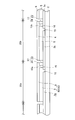
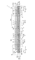
- FIG. 2 is a cross-sectional view in the XX direction of FIG.
- FIG. 2 is a cross-sectional view in the YY direction of FIG.
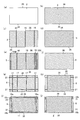
- FIG. 1 is a view at the start of the first electrode layer stacking step
- (b) is a view at the start of the first laser scribing step
- (c) is a view at the start of the functional layer stacking step
- (d) is the first view.
- the figure at the end of the two laser scribe process (e) is the figure at the start of the second electrode layer laminating process
- (f) is the figure at the start of the third laser scribe process
- (g) is the protective member laminating process.
- the figure at the start (h) is the figure at the start of the fourth laser scribe process, (i) is the figure at the start of the sealing process, and (j) is the figure at the end of the sealing process.
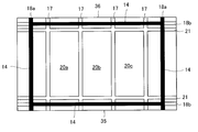
- region of FIG. It is the front view which displayed the area
- sectional drawing which shows the layer structure of the organic EL element part of 1st Embodiment of this invention.
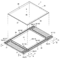
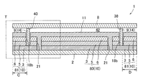
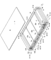
- FIG. 1 shows an organic EL device 1 according to the first embodiment of the present invention.
- the positional relationship between the top, bottom, left, and right will be described based on the posture of FIG. 1 unless otherwise specified.
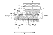
- the organic EL device 1 of the present embodiment is provided with a flat sealing member 8 on the back surface (upper side of the drawing) of the substrate 2 (base material) as in the prior art, and the organic EL element is formed by the sealing member 8.
- the part 10 is covered with the protective layer 11, and the organic EL element part 10 is shielded from the outside by the sealing member 8.
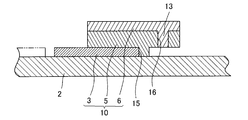
- a portion where three layers of the first electrode layer 3, the functional layer 5, and the second electrode layer 6 are laminated is referred to as an organic EL element portion 10.
- the organic EL element unit 10 includes a light emitting organic EL element region 80 and a non-light emitting organic EL element region 81.
- the light emitting organic EL element region 80 is the organic EL element portion 10 that actually emits light
- the non-light emitting organic EL element region 81 is the organic EL element portion 10 that does not actually emit light other than the light emitting organic EL element region 80.
- an insulating adhesive material 9 (connecting portion) mainly composed of glass frit is used.
- the main component here means that the mass percent concentration with respect to all the components is 50 percent or more and 100 percent or less.
- the mass percent concentration of the glass frit with respect to all the components occupies 70% or more, more preferably 80% or more, and particularly preferably 90% or more.
- the layer structure of the organic EL element part (excluding the protective layer 11) 10 of the organic EL device 1 is as shown in FIGS. 3, 4, and 5.
- the substrate 2 base material
- the first electrode layer 3 and The functional layer 5 (organic light emitting layer) and the second electrode layer 6 are stacked in this order.
- the organic EL device 1 of the present embodiment has a structure in which a protective layer 11 is further laminated on the organic EL element unit 10 shown in FIGS. 3, 4, and 5 as shown in FIGS. Furthermore, these are sealed by the sealing member 8 via the insulating adhesive material 9.
- the substrate 2 is rectangular, and the organic EL element unit 10 is provided thereon.
- a light emitting organic EL element region 80 (including the protective layer 11) that actually emits light is provided at the center of the substrate 2. That is, the first electrode layer 3, the functional layer 5 (organic light emitting layer), and the second electrode layer 6 are provided on the substrate 2, and a protective layer 11 is further laminated on the central portion of the substrate 2. Has been.
- the organic EL element portion 10 is formed on substantially the entire surface of the substrate 2 as shown in FIG. 2, and a part of the organic EL element portion 10 is removed in a groove shape. That is, in the organic EL device 1 of the present embodiment, there is an organic EL element portion 10 (light emitting organic EL element region 80) that actually emits light only at the central portion of the substrate 2.
- non-light-emitting protrusions A and B non-light-emitting organic EL element region 81 that protrude from the light-emitting organic EL element region 80 at both ends in the longitudinal direction of the organic EL device 1, and the short-side substrate
- the organic EL element part 10 exists on 2 except a groove
- the protruding portions A and B are provided with a frit fixing separation groove 18a from which at least a layer located above the first electrode layer 3 is removed. Therefore, immediately after the frit fixing separation groove 18a is formed, the first electrode layer 3 is exposed at the bottom of the frit fixing separation groove 18a.
- non-light-emitting protrusions C and D are provided in the vicinity of the end of the substrate 2 in the short direction as shown in FIGS.
- the protruding portions C and D the first electrode layer 3 and other layers are present. Therefore, when the functional layer 5 and other layers are formed by using the laser scribing process, it is possible to omit a mask process that hides a film formation surface on which the film formation is not performed.
- the protruding portions C and D are provided with a frit fixing separation groove 18b (outer transverse groove) from which at least a layer located above the first electrode layer 3 is removed.
- the intrusion prevention separation groove 21 inner transverse groove in which the first electrode layer 3 and other layers are not present in the protruding portions C and D is parallel to the longitudinal sides 35 and 36 of the substrate 2. Exists.
- the intrusion prevention separation groove 21 also has no first electrode layer 3.
- the first electrode layer 3 and the first electrode layer 3 are arranged in the vicinity of both ends of the organic EL element unit 10 in parallel with the longitudinal sides 35 and 36.
- An intrusion prevention separation groove 21 (inner transverse groove) from which three layers of the two-electrode layer 6 and the functional layer 5 are removed is provided.
- the intrusion preventing separation groove 21 is a laminate from the protruding portion A having the second electrode layer 6M (first electrode communication portion) to the protruding portion B having the second electrode layer 6N (second electrode communication portion). This is a transverse groove that crosses the organic EL element portion 10. Further, the intrusion prevention separation groove 21 is located inside the frit fixing separation groove 18b.
- the frit fixing separation grooves 18a and 18b extend in directions intersecting each other. Specifically, the frit fixing separation groove 18a extends in a direction orthogonal to the frit fixing separation groove 18b. Further, the bonding portions 37, 38, 39, and 40 of the sealing member 8 are bonded to the frit fixing separation grooves 18a and 18b. That is, the sealing member 8 is formed of an insulating material and has a main body portion 41 that is rectangular in plan view. Further, the insulating adhesive material 9 is formed thick in the frit fixing separation grooves 18 a and 18 b, and a gap maintaining space 42 is formed between the sealing member 8 and the organic EL element portion 10.
- the gap maintaining space 42 is filled with an inert gas such as nitrogen or argon. Further, it is preferable to put a desiccant that absorbs moisture and oxygen into the gap maintaining space 42. Then, the vertical adhesive portions 37 and 39 of the sealing member 8 are bonded to the frit fixing separation grooves 18a as shown in FIG. 8 through the insulating adhesive material 9 as shown in FIG. Further, the lateral adhesive portions 38 and 40 of the sealing member 8 are adhered to the frit fixing separation grooves 18b in FIG. 8 through the insulating adhesive material 9 (connection portion) as shown in FIG. .
- an inert gas such as nitrogen or argon.
- the adhesive portions 37 and 39 on the vertical side of the sealing member 8 are bonded to the frit fixing separation groove 18a as described above, as shown in FIG.
- the organic EL element part 10 is exposed outside the member 8. That is, as described above, the light-emitting organic EL element region 80 has non-light-emitting protrusions A and B (non-light-emitting organic EL element region 81). It is exposed outside the sealing member 8 (FIG. 2).
- the laminated structure of one outer edge E is a laminated structure of the organic EL element part 10 as shown in FIGS. 6 and 10, and the first functional layer separation groove 16M is arranged outside the frit fixing separation groove 18a. ing.
- the laminated structure of the outer edge portion F located on the opposite side is the laminated structure of the organic EL element part 10 as shown in FIGS. 6 and 11, and the first functional layer separating groove 16N is provided outside the frit fixing separating groove 18a. It is arranged.
- the second electrode layer 6M at the outer edge E is electrically connected to the first electrode layer 3a in the light emitting organic EL element region 80 (FIG. 10).
- the first electrode layer 3d at the outer edge F is directly connected to the second electrode layer 6 in the light emitting organic EL element region 80 inside the sealing member 8, and the second electrode layer 6N outside the sealing member 8.
- the second electrode communication portion is electrically connected in series (FIG. 11).
- the organic EL element unit 10 employed in the present embodiment is an integrated organic EL element.
- the integrated organic EL element is an organic EL element formed in a strip shape (hereinafter referred to as “unit EL element”) electrically connected in series.
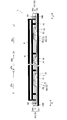
- the basic layer structure of the organic EL element unit 10 is as shown in FIGS. 3 and 4.
- a plurality of grooves are provided, and one planar organic EL element unit 10 is a strip-shaped unit EL element 20 a, It is divided into 20b. That is, the organic EL element unit 10 is formed by sequentially laminating the first electrode layer 3, the functional layer 5, and the second electrode layer 6 on the substrate 2.
- the functional layer 5 is a stacked body layer including a plurality of organic compound layers, and is formed by stacking, for example, a hole injection layer, a hole transport layer, a light emitting layer, an electron transport layer, and a conductive layer.
- the first electrode layer separation groove 15, the first functional layer separation groove 16, the second functional layer separation groove 23, and the second electrode layer separation groove 24 are formed in each layer. Has been.
- the first electrode layer separation groove 15 is formed in the first electrode layer 3, and the first electrode layer 3 is divided into a plurality of parts.
- a first functional layer separation groove 16 is formed in the functional layer 5, and the functional layer 5 is divided into a plurality of parts.
- a part of the second electrode layer 6 enters the first functional layer separation groove 16 and is in contact with the first electrode layer 3 at the bottom of the groove. That is, the first functional layer separation groove 16 is a conductive opening provided in the functional layer 5, and a part of the second electrode layer 6 penetrates into the conductive opening, and the first electrode layer 3 and the first electrode layer 3 are formed at the bottom of the groove. It touches.
- the organic EL device 1 includes a first electrode layer separation groove 15 provided in the first electrode layer 3 and a unit EL element separation groove 17 provided in the functional layer 5 and the second electrode layer 6.
- Each thin layer is partitioned and independent unit EL elements 20a, 20b, 20c... Are formed. That is, as shown in FIG. 3, one of the plurality of first electrode layers 3 defined by the first electrode layer separation grooves 15 and the functional layer 5 stacked on the partitioned first electrode layer 3 are provided.
- a unit EL element 20 is constituted by the section of the second electrode layer 6.
- One unit EL element 20a is electrically connected in series with the adjacent unit EL element 20b. That is, since the first electrode layer separation groove 15 and the first functional layer separation groove 16 are at different positions, the functional layer 5 belonging to one unit EL element 20a and the second electrode layer 6 are formed by the first electrode layer. It protrudes from 3a and straddles adjacent unit EL elements 20b. The intrusion portion 13a that has entered the first functional layer separation groove 16 of the second electrode layer 6 is in contact with the first electrode layer 3b of the adjacent unit EL element 20b. As a result, the unit EL element 20a on the substrate 2 is connected in series with the unit EL element 20b through the penetration part 13a of the second electrode layer 6.
- the terminal 60 connected to the external power source is connected to the second electrode layer 6M located at the outer edge E of the protruding portion A (non-light emitting organic EL element region 81).
- the terminal 61 connected to the external power source is connected to the second electrode layer 6N located at the outer edge F of the protruding portion B (non-light emitting organic EL element region 81).
- the second electrode layer 6M is electrically connected in series with the adjacent unit EL element 20a.
- the intrusion portion 13M in which the second electrode layer 6M belonging to the outer edge portion E enters the first functional layer separation groove 16M is in contact with the first electrode layer 3a. Yes.
- the terminal 60 connected to the external power source is connected to the second electrode layer 6M, and connected in series with the unit EL element 20a via the intrusion portion 13M of the second electrode layer 6M and the first electrode layer 3a. Yes.
- the first electrode layer 3d As shown in FIGS. 6 and 11, at the outer edge portion F, a part of the second electrode layer 6N enters the first functional layer separation groove 16N, and the first electrode layer 3d becomes the second electrode layer 6N ( A part of the second electrode communication portion). As a result, the first electrode layer 3d extending from the light emitting organic EL element region 80 is connected in series with the terminal 61 via the intrusion portion 13N of the second electrode layer 6N at the outer edge portion F.
- FIG. 12 shows an actual current flow with arrows.
- the current supplied from the external power source flows from the terminal 60 connected to the external power source to the second electrode layer 6M belonging to the outer edge E, and then the first electrode in the light emitting organic EL element region 80 from the second electrode layer 6M. It flows toward the layer 3a. That is, a part of the second electrode layer 6M is in contact with the adjacent first electrode layer 3a through the intrusion portion 13M in the first functional layer separation groove 16M, and in the light emitting organic EL element region 80 through the intrusion portion 13M. A current flows through the first electrode layer 3a.
- the first electrode layer 3 a flows from the first electrode layer 3 a to the second electrode layer 6 through the functional layer 5, but a part of the second electrode layer 6 is in the first functional layer separation groove 16. Is in contact with the adjacent first electrode layer 3b through the intrusion portion 13a, and a current flows through the first unit EL element 20a to the first electrode layer 3b of the adjacent unit EL element 20b. Thereafter, a current flows between the unit EL elements 20 similarly to the above, and reaches the first electrode layer 3d.
- the above is the description of the layer configuration of the organic EL element unit 10.
- a method for manufacturing the organic EL device 1 according to this embodiment will be described.
- the organic EL device 1 is manufactured using a vacuum vapor deposition device (not shown) and a laser scribing device (not shown).
- a step of laminating the first electrode layer 3 on the substrate 2 is performed. (FIG. 13 (a) to FIG. 13 (b))
- the first electrode layer 3 is formed by sputtering or CVD.
- the first electrode layer 3 is preferably indium tin oxide (ITO) by sputtering or ion plating, or zinc oxide by low pressure thermal CVD among the CVD methods.
- ITO indium tin oxide
- the average thickness of the first electrode layer 3 is preferably 30 ⁇ m to 500 ⁇ m.
- first laser scribing process is performed to form a first electrode layer separation groove 15 in the first electrode layer 3.
- the first electrode layer separation grooves 15 are respectively formed in the vertical direction of the drawing and are parallel to each other.
- the laser scribing device has an XY table, a laser generator, and an optical system member.
- the first laser scribing step is performed by placing the substrate 2 on an XY table and moving the substrate 2 linearly at a constant speed in the vertical direction while irradiating a laser beam. Then, the X / Y table is moved in the horizontal direction to shift the irradiation position of the laser beam, and the substrate 2 is linearly moved again in the vertical direction while irradiating the laser beam.
- the surface of the substrate is sometimes cleaned.
- the functional layer 5 is formed on the entire surface by sequentially depositing the hole injection layer 28, the hole transport layer 27, the light emitting layer 26, the electron transport layer 25, and the like on this substrate by vacuum vapor deposition.
- the hole injection layer 28 the hole transport layer 27, the light emitting layer 26, the electron transport layer 25, and the like on this substrate by vacuum vapor deposition.
- the first functional layer separation grooves 16 are formed in the vertical direction of the drawing and are parallel to each other. Further, the first functional layer separation groove 16 is shifted from the first electrode layer separation groove 15 by a predetermined distance.
- a third laser scribing step is performed to form unit EL element isolation grooves 17 that extend over both the functional layer 5 and the second electrode layer 6. Further, before and after that, an intrusion prevention separation groove 21 (inner transverse groove) is formed across three layers of the first electrode layer 3, the functional layer 5, and the second electrode layer 6. (FIG. 13 (f) to FIG. 13 (g))
- the unit EL element separation grooves 17 are formed in the vertical direction of the drawing, and are parallel to each other. Further, the intrusion prevention separation groove 21 is formed in a direction (left and right direction in the drawing) orthogonal to the unit EL element separation groove 17. As shown in FIGS.
- the intrusion prevention separation groove 21 is formed over three layers of the first electrode layer 3, the functional layer 5, and the second electrode layer 6.
- the presence of the intrusion prevention separation groove 21 can prevent intrusion of water or the like into the functional layer 5. That is, by operating the organic EL device 1 for a long period of time, the insulating adhesive material 9 deteriorates, moisture enters the organic EL element portion 10, and the penetrated moisture further interfaces with the layers of the organic EL element portion 10.
- Intrusion prevention separation grooves 21 are formed over the three layers of the first electrode layer 3, the functional layer 5, and the second electrode layer 6, so that the intrusion of moisture into the power generation unit can be prevented.
- the protective layer 11 is formed on the second electrode layer 6.
- the protective layer 11 may be formed on the entire surface, but it is preferable not to form the protective layer 11 on both the left and right sides of the drawing for taking out the electrodes. (Protective member laminating step) (FIG. 13 (g) to FIG. 13 (h))
- a fourth laser scribing step is performed to form frit fixing separation grooves 18a and 18b from which at least the layer above the functional layer 5 is removed in the non-light emitting portion.
- the frit fixing separation groove 18a is formed in the vertical direction, and the frit fixing separation groove 18b is formed in the left and right direction.
- the frit fixing separation grooves 18a and 18b are parallel to each other.
- an insulating glass frit 14 is disposed in the frit fixing separation grooves 18a and 18b. That is, the insulating glass frit 14 is disposed at the black solid portion shown in FIG.
- the insulating glass frit 14 is sequentially irradiated with a laser beam to melt the glass frit 14. That is, only the glass frit 14 is partially heated to melt the insulating glass frit 14 in the frit fixing separation grooves 18 a and 18 b to bond the first electrode layer 3 and the sealing member 8. In this way, the sealing member 8 is adhered and the sealing operation is performed to complete the organic EL device. (FIGS. 13 (i) to 13 (j)) (sealing process)
- the shape of the sealing member 8 is a flat plate, but the shape of the sealing member 8 is not particularly limited.
- the insulating adhesive material 9 can be made thin, and the intrusion of moisture due to the deterioration of the insulating adhesive material 9 can be suppressed.
- the gap maintaining space 42 is filled with an inert gas, but the present invention is not limited to this, and a resin is mixed with a desiccant or an oxygen scavenger that absorbs moisture or oxygen.
- the space maintaining space 42 may be filled.
- the material of the substrate 2 is not particularly limited, and a substrate having transparency is adopted.
- a flexible film substrate or a plastic substrate is appropriately selected and used.
- a glass substrate or a film substrate is particularly preferable from the viewpoints of transparency and workability.
- the material of the film substrate includes a thermoplastic resin and a thermosetting resin.
- the thermoplastic resin include acrylic resin, polyester, polycarbonate resin, polyolefin, and cycloolefin polymer.
- An example of the thermosetting resin is polyurethane.
- a substrate composed mainly of a cycloolefin polymer (COP) having both excellent optical isotropy and water vapor barrier properties is preferred.
- COP examples include norbornene polymers, copolymers of norbornene and olefins, and polymers of unsaturated alicyclic hydrocarbons such as cyclopentadiene. From the viewpoint of water vapor barrier properties, it is preferable that the main chain and side chain of the constituent molecules do not contain a functional group having a large polarity, such as a carbonyl group or a hydroxyl group.
- the thickness of the film substrate is preferably about 0.03 mm to 3.0 mm. This film thickness range is preferable from the viewpoint of the strength against bending and scratching of the substrate, in addition to the ease of handling of the substrate and the weight at the time of device fabrication.
- PEN polyethylene naphthalate
- PES polyethersulfone
- the material of the first electrode layer 3 is not particularly limited.
- a metal such as indium tin oxide (ITO), indium zinc oxide (IZO), tin oxide (SnO 2 ), or zinc oxide (ZnO) is used.
- An oxide or a metal such as silver (Ag) or chromium (Cr) is employed.
- ITO or IZO having high transparency can be used particularly preferably.
- the functional layer 5 has an electron transport layer 25, a light emitting layer 26, a hole transport layer 27, and a hole injection layer 28 stacked in this order from the second electrode layer 6 side. It has a structure.
- a known substance can be used as the material of the electron transport layer 25 .
- An azole, an oxadiazole derivative, a bis (10-hydroxybenzo [h] quinolinolato) beryllium complex, a triazole compound, or the like can be used, but the invention is not limited thereto.
- a known substance can be used as the material of the light emitting layer 26, a known substance can be used.
- 9,10-diarylanthracene derivatives, pyrene, coronene, perylene, rubrene, 1,1,4,4-tetraphenylbutadiene tris (8-quinolinolato) aluminum complex, tris (4-methyl-8-quinolinolato) aluminum Complex, bis (8-quinolinolato) zinc complex, tris (4-methyl-5-trifluoromethyl-8-quinolinolato) aluminum complex, tris (4-methyl-5-cyano-8-quinolinolato) aluminum complex, bis (2 -Methyl-5-trifluoromethyl-8-quinolinolato) [4- (4-cyanophenyl) phenolate] aluminum complex, bis (2-methyl-5-cyano-8-quinolinolato) [4- (4-cyanophenyl) Phenolate] aluminum complex, tris (8-ki Linolato) scandium complex
- metal phthalocyanines such as copper phthalocyanine and tetra (t-butyl) copper phthalocyanine and metal-free phthalocyanines, quinacridone compounds, 1,1-bis (4-di-p-tolylaminophenyl) cyclohexane, N, N′— Diphenyl-N, N′-bis (3-methylphenyl) -1,1′-biphenyl-4,4′-diamine, N, N′-di (1-naphthyl) -N, N′-diphenyl-1, Aromatic amine low molecular hole injection and transport materials such as 1'-biphenyl-4,4'-diamine, polyaniline, polythiophene, polyvinylcarbazole, poly (3,4-ethylenedioxythiophene) and polystyrenesulfonic acid Polymer hole transport layer materials such as mixtures
- a known substance can be used as the material of the hole injection layer 28 .
- the constituent layers of these functional layers 5 are well-known as appropriate, such as vacuum deposition, sputtering, CVD, dipping, roll coating (printing), spin coating, bar coating, spraying, die coating, and flow coating.
- the film can be formed by this method.
- a known substance can be used as the material of the second electrode layer 6.
- examples thereof include silver and aluminum. These materials are preferably deposited by sputtering or vacuum evaporation.
- metal oxides such as silicon oxide, aluminum oxide, chromium oxide, and magnesium oxide
- metal fluorides such as aluminum fluoride, magnesium fluoride, and calcium fluoride
- metal nitrides such as silicon nitride, aluminum nitride, and chromium nitride
- Metal oxynitrides such as silicon oxynitride, DLC (diamond-like carbon), inorganic materials such as amorphous silicon film
- polyesters such as polyethylene terephthalate (PET) and polyethylene naphthalate (PEN), polyethylene, polypropylene, cellophane, cellulose Cellulose esters such as diacetate, cellulose triacetate, cellulose acetate butyrate, cellulose acetate propionate (CAP), cellulose acetate phthalate, and cellulose nitrate Derivatives thereof, polyvinylidene chloride, polyvinyl alcohol, polyethylene vinyl alcohol
- the protective layer 11 is preferably a material having a gas barrier property and / or a hygroscopic property.
- the “gas barrier property” represents a property of blocking the ingress of gases such as oxygen and nitrogen.
- the protective layer 11 preferably has an oxygen gas barrier property.
- film forming methods such as resistance heating vapor deposition, electron beam vapor deposition, reactive vapor deposition, ion plating, sputtering, and CVD can be used depending on the material.
- polyesters such as polyethylene terephthalate (PET) and polyethylene naphthalate (PEN), polyethylene, polypropylene, cellophane, cellulose diacetate, cellulose triacetate, cellulose acetate butyrate, cellulose acetate propionate (CAP), cellulose acetate phthalate (TAC) ), Cellulose esters such as cellulose nitrate or derivatives thereof, polyvinylidene chloride, polyvinyl alcohol, polyethylene vinyl alcohol, syndiotactic polystyrene, polycarbonate, norbornene resin, polymethylpentene, polyetherketone, polyimide, polyethersulfone ( PES), polyphenylene sulfide, polysulfones, polyetherimide, Metal film of aluminum, copper, nickel, stainless steel, etc.
- PET polyethylene terephthalate
- PEN polyethylene naphthalate
- CAP cellulose acetate propionate
- TAC cellulose acetate phthalate
- metal foil or resin film such as polyether ketone imide, polyamide, fluororesin, nylon, polymethyl methacrylate, acrylic or polyarylate, cycloolefin resin, aluminum or stainless steel
- a laminated film can be used, the present invention is not limited to these.
- Organic EL device 1 Organic EL device 2 Substrate (base material) 3 First electrode layer 5 Functional layer (organic light emitting layer) 6 2nd electrode layer 6M 2nd electrode layer (1st electrode communication part) 6N second electrode layer (second electrode communication part) 8 Sealing member 9 Insulating adhesive material (connection part) 10 Organic EL element part (laminated body) 14 Insulating frit (adhesive material) 16M, 16N First functional layer separation groove (opening for conduction) 18b Separation groove for fixing frit (outer transverse groove, second transverse groove) 20 Unit EL element 21 Intrusion prevention separation groove (inner transverse groove, first transverse groove)
Landscapes
- Physics & Mathematics (AREA)
- Optics & Photonics (AREA)
- Engineering & Computer Science (AREA)
- Manufacturing & Machinery (AREA)
- Electroluminescent Light Sources (AREA)
Abstract
有用な態様の光を高効率で取り出すことができる有機EL装置を提供する。 基板2上に第1電極層3と、機能層5と、第2電極層6が積層されて有機EL素子部10を形成し、有機EL素子部10が封止部材8で封止された有機EL装置1において、基板2の一辺側に第1電極層3と電気的に接続されてなる第2電極層6Mがあり、基板2の対向する辺側に第2電極層6と電気的に接続された第2電極層6Nがあり、第2電極層6Mから第2電極層6Nにかけて有機EL素子部10を横断する第1横断溝21が設けられ、当該第1横断溝21は、第1電極層3と、機能層5と、第2電極層6のいずれもが除去されており、前記封止部材8と基板2との接続部は前記第1横断溝21よりも外側の位置にある構成としている。
Description
本発明は、有機EL(Electro Luminescence)装置に関するものである。
近年、白熱灯や蛍光灯に代わる照明装置として有機EL装置が注目され、多くの研究がなされている。また、テレビに代表されるディスプレイ部材においても液晶方式やプラズマ方式に変わる方式として有機EL方式が注目されている。
ここで、有機EL装置は、ガラス基板や透明樹脂フィルム等の基材に、有機EL素子を積層したものである。
また、有機EL素子は、一方又は双方が透光性を有する2つの電極を対向させ、この電極の間に有機化合物からなる発光層を積層したものである。有機EL装置は、電気的に励起された電子と正孔との再結合のエネルギーによって発光する。
有機EL装置は、自発光デバイスであるため、ディスプレイ材料として使用すると高コントラストの画像を得ることができる。また、発光層の材料を適宜選択することにより、種々の波長の光を発光することができる。また、白熱灯や蛍光灯に比べて厚さが極めて薄く、且つ面状に発光するので、設置場所の制約が少ない。
また、有機EL素子は、一方又は双方が透光性を有する2つの電極を対向させ、この電極の間に有機化合物からなる発光層を積層したものである。有機EL装置は、電気的に励起された電子と正孔との再結合のエネルギーによって発光する。
有機EL装置は、自発光デバイスであるため、ディスプレイ材料として使用すると高コントラストの画像を得ることができる。また、発光層の材料を適宜選択することにより、種々の波長の光を発光することができる。また、白熱灯や蛍光灯に比べて厚さが極めて薄く、且つ面状に発光するので、設置場所の制約が少ない。
ところで、有機EL素子は、一定期間駆動した場合、発光輝度、発光効率、発光均一性等の発光特性が初期の場合に比べて著しく劣化するという問題がある。このような発光特性の劣化の原因としては、有機EL素子内に侵入した酸素による電極の酸化、駆動時の発熱による有機材料の酸化分解、有機EL素子内に侵入した空気中の水分による電極の酸化、有機物の変性等を挙げることができる。さらに、酸素や水分の影響で構造体の界面が剥離したり、駆動時の発熱や駆動時の環境が高温であったこと等が引き金となり、さらに各構成要素の熱膨張率の違いにより構造体の界面で応力が発生し、界面が剥離したりする等の構造体の機械的劣化も発光特性の劣化の原因として挙げることができる。
即ち、有機EL装置の劣化防止のためには、有機EL素子への水等の液体や酸素等の気体の侵入を防ぐ必要がある。
このような問題を防止するため、有機EL素子を樹脂製の接着剤を用いて封止し、水分や酸素との接触を防止する技術が提案されている。
例えば、酸素及び水分による劣化を防止する技術として、有機EL素子の基板上に形成された発光層の上方の位置に封止部材をかぶせ、それを接着剤で封止し、さらに、封止空間内に吸湿作用のある吸着剤等を封入するなどの対策が採られている。(特許文献1)
しかしながら、従来の接着剤を使った封止では、有機EL装置を長時間駆動させると接着剤部分から水分等が透過し、所望の封止性能が十分得られなかった。そのため、水分等の侵入による発光特性の低下の懸念が未だ残っている。
そこで、本発明は、上記した問題点を解決するものであり、有機EL装置の発光部位への水分等の侵入を防止することができる有機EL装置を開発することを課題とするものである。
上記課題を解決するための本発明の様相は、基材上に第1電極層と、有機発光層と、第2電極層が積層されて積層体を形成し、前記積層体が封止部材で封止された有機EL装置において、基材の一辺側に第1電極層と電気的に接続されてなる第一電極連通部があり、基材の対向する辺側に第2電極層と電気的に接続された第二電極連通部があり、第一電極連通部から第二電極連通部にかけて積層体を横断する第1横断溝(内側横断溝)が設けられ、当該第1横断溝は、第1電極層と、有機発光層と、第2電極層のいずれもが除去されており、前記封止部材と基材との接続部は前記第1横断溝よりも外側の位置にあることを特徴とする有機EL装置である。ここで、「電気的に接続」とは、直接的に接続されている構成のみならず、間接的に接続されている構成も含む。
かかる構成によれば、前記封止部材と基材との接続部は前記第1横断溝よりも外側の位置にあるため、例え接続部を超えて有機EL装置内部に水等が侵入しても内側に位置する第1横断溝により、有機EL装置の発光部位への水等の移動を防止することができる。即ち、有機EL装置の長寿命化が可能である。
本発明の有機EL装置において、第1横断溝よりも外側の位置に第2横断溝(外側横断溝)が設けられ、当該第2横断溝は、少なくとも有機発光層と、第2電極層が除去されており、当該第2横断溝に接着材料が配されて封止部材が取り付けられていることが好ましい。
かかる構成によれば、当該第2横断溝に接着材料が配されて封止部材が取り付けられているため、水等の液体が封止部材の内側に侵入しにくく、有機EL装置の発光部位への侵入をさらに高度に防止できる。
本発明の有機EL装置は、前記第2横断溝と交差する方向に第1縦断溝を有し、当該第1縦断溝は、少なくとも有機発光層と、第2電極層が除去されており、当該第1縦断溝内には、少なくとも第1電極層が積層しており、当該第1縦断溝に接着材料が配されて封止部材が取り付けられていることが好ましい。
前記第1縦断溝及び第2横断溝は、レーザスクライブ処理によって形成されており、前記第1縦断溝の底面の一部または全部は、前記第2横断溝と同一の層構成を有していることが好ましい。
また、本発明の有機EL装置において、第1電極層と、有機発光層と、第2電極層には溝が形成されていて複数の単位EL素子に分割されており、当該単位EL素子が電気的に直列に接続されてなることが好ましい。
かかる構成によれば、複数の単位EL素子を均一に発光させることができる。
また、本発明の有機EL装置において、第1電極層は封止部材の内側から外側に伸延しており、前記第1電極層は封止部材の内側では第2電極層と直接接続されており、封止部材の外側では第二電極連通部と電気的に直列に接続されていることが好ましい。
かかる構成によれば、有機EL装置内への電流の供給が容易である。
封止部材は絶縁材料で成形されたものであることが好ましい。
また、封止部材は、絶縁性接着材料によって、接着されていることが好ましい。
前記絶縁性接着材料は、ガラスフリットを主成分とすることが好ましい。
前記第1横断溝は、レーザスクライブ処理によって形成されていることが好ましい。
前記第1横断溝の外側には、非発光の非発光有機EL素子領域があり、前記非発光有機EL素子領域には、第1電極層と、有機発光層と、第2電極層とが積層していることが好ましい。
前記第1横断溝の底面の一部又は全部は、ガスバリア性及び/又は吸湿性を有する保護層が積層していることが好ましい。
本発明に係る構成を用いれば、前記封止部材と基材との接続部は前記第1横断溝よりも外側の位置にあるため、例え接続部を超えて有機EL装置内部に水等が侵入しても内側に位置する第1横断溝により、有機EL装置の発光部位への水等の移動を防止することができる。即ち、有機EL装置の長寿命化が可能である。
本発明は、有機EL装置に係るものである。図1は、本発明の第1実施形態に係る有機EL装置1を示している。以下、上下左右の位置関係は、特に断りのない限り、図1の姿勢を基準に説明する。
本実施形態の有機EL装置1は、従来技術と同様に、基板2(基材)の背面(図面上側)に平板状の封止部材8を設けており、当該封止部材8で有機EL素子部10を保護層11ごと覆い、封止部材8によって有機EL素子部10を外部と遮蔽するものである。(図1、図2)
なお、本実施形態では、第1電極層3と、機能層5と、第2電極層6との3層が積層した部分を有機EL素子部10と称している。また、有機EL素子部10は発光有機EL素子領域80と非発光有機EL素子領域81を有している。発光有機EL素子領域80は実際に発光する有機EL素子部10であり、非発光有機EL素子領域81は発光有機EL素子領域80以外の実際に発光しない有機EL素子部10である。
また、封止部材8と基板2とを接着する手段として、ガラスフリットを主成分とする絶縁性接着材料9(接続部)を使用している。
ここでいう主成分とは、全成分に対する質量パーセント濃度が、50パーセント以上100パーセント以下であることを表す。絶縁性接着材料9としては、全成分に対するガラスフリットの質量パーセント濃度が70パーセント以上を占めることが好ましく、80パーセント以上を占めることがより好ましく、90パーセント以上を占めることが特に好ましい。
有機EL装置1の有機EL素子部(保護層11を除く)10の層構成は、図3、図4、図5の通りであり、基板2(基材)上に、第1電極層3と、機能層5(有機発光層)と、第2電極層6と、がこの順番に積層された構造を有している。
そして、本実施形態の有機EL装置1は、図3、図4、図5に示した有機EL素子部10にさらに図6、図7の様に保護層11が積層された構造を有しており、さらにこれらが絶縁性接着材料9を介して封止部材8によって封止されている。
そして、本実施形態の有機EL装置1は、図3、図4、図5に示した有機EL素子部10にさらに図6、図7の様に保護層11が積層された構造を有しており、さらにこれらが絶縁性接着材料9を介して封止部材8によって封止されている。
説明の都合上、まず初めに本実施形態の特徴的構成について説明する。なお、有機EL素子部10の詳細な説明は後述する。
本実施形態の有機EL装置1では、図2に示すように、基板2が長方形であり、その上に有機EL素子部10が設けられている。また、基板2の中央部に実際に発光する発光有機EL素子領域80(保護層11も含む)が設けられている。即ち、基板2上に、前記した第1電極層3と、機能層5(有機発光層)と、第2電極層6が設けられ、基板2の中央部では、さらにこれらに保護層11が積層されている。
そして、本実施形態の有機EL装置1では、図2の様に有機EL素子部10が基板2の略全面に成膜されており、その一部分が溝状に除去されている。
即ち、本実施形態の有機EL装置1では、基板2の中央部にだけ実際に発光する有機EL素子部10(発光有機EL素子領域80)がある。詳説すると、有機EL装置1の長手方向の両端部には発光有機EL素子領域80からはみ出した非発光のはみ出し部分A、B(非発光有機EL素子領域81)が存在し、短手方向の基板2上には溝を除いて有機EL素子部10が存在している。そのため、レーザスクライブ処理を用いることで、有機EL素子部10を成膜する際に、成膜を行わない被成膜面を隠すマスクプロセスを省略できる。
そして、当該はみ出し部分A、Bには、少なくとも第1電極層3より上方に位置する層を除去したフリット固定用分離溝18aが設けられている。
従って、フリット固定用分離溝18aを形成した直後は、フリット固定用分離溝18aの底部は第1電極層3が露出した状態となっている。
有機EL装置1の短手方向に目を移すと、図2、図8、図9の様に基板2の短手方向の端部近傍に非発光のはみ出し部分C、Dが設けられている。
はみ出し部分C、Dには第1電極層3並びにその他の層が存在している。そのため、レーザスクライブ処理を用いることで、機能層5並びにその他の層を成膜する際に、成膜を行わない被成膜面を隠すマスクプロセスを省略できる。
また、当該はみ出し部分C、Dには、少なくとも第1電極層3より上方に位置する層を除去したフリット固定用分離溝18b(外側横断溝)が設けられている。
従って、フリット固定用分離溝18bを形成した直後は、フリット固定用分離溝18bの底部は第1電極層3が露出した状態となっている。
そして、本実施形態では、基板2の長手方向の辺35、36と平行に、はみ出し部分C、Dに第1電極層3並びにその他の層が存在しない侵入防止分離溝21(内側横断溝)が存在する。この侵入防止分離溝21には、第1電極層3も無い。
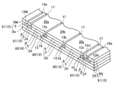
即ち、本実施形態の有機EL装置1では、図8、図9の様に、有機EL素子部10の両端部付近に、長手方向の辺35、36と平行に、第1電極層3と第2電極層6と機能層5の3層を除去した侵入防止分離溝21(内側横断溝)が設けられている。
侵入防止分離溝21(内側横断溝)は、第2電極層6M(第一電極連通部)を有するはみ出し部分Aから第2電極層6N(第二電極連通部)を有するはみ出し部分Bにかけて積層体である有機EL素子部10を横断する横断溝である。また、侵入防止分離溝21はフリット固定用分離溝18bの内側に位置している。
侵入防止分離溝21(内側横断溝)は、第2電極層6M(第一電極連通部)を有するはみ出し部分Aから第2電極層6N(第二電極連通部)を有するはみ出し部分Bにかけて積層体である有機EL素子部10を横断する横断溝である。また、侵入防止分離溝21はフリット固定用分離溝18bの内側に位置している。
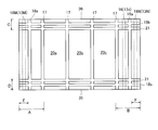
そして、本実施形態では、図2、図6、図7、図9の様に、前記したフリット固定用分離溝18a、18bは、互いに交差する方向に延伸している。具体的には、フリット固定用分離溝18aは、フリット固定用分離溝18bに対して直交する方向に延伸している。 また、フリット固定用分離溝18a、18bには、封止部材8の接着部37、38、39、40が接着されている。
即ち、封止部材8は、絶縁材料で成形されたものであり、平面視が長方形の本体部41を有している。また、フリット固定用分離溝18a、18bには、絶縁性接着材料9が厚く形成されており、封止部材8と有機EL素子部10との間に間隔維持空間42を形成している。間隔維持空間42は窒素やアルゴンなどの不活性ガスで満たされている。また、間隔維持空間42には、水分や酸素を吸収する乾燥材を入れることが好ましい。
そして、図8の縦列たるフリット固定用分離溝18aに、図6のように絶縁性接着材料9を介して封止部材8の縦側の接着部37、39が接着されている。
また、図8の横列たるフリット固定用分離溝18bに、図7のように絶縁性接着材料9(接続部)を介して封止部材8の横側の接着部38、40が接着されている。
本実施形態の有機EL装置1では、前記した様にフリット固定用分離溝18aに封止部材8の縦側の接着部37、39が接着されているから、図1に示すように、封止部材8の外側に、有機EL素子部10が露出する。即ち、前記した様に、発光有機EL素子領域80からはみ出した非発光のはみ出し部分A、B(非発光有機EL素子領域81)を有し、当該はみ出し部分A、Bの外縁部E、Fは、封止部材8の外側に露出している(図2)。
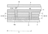
そして、一方の外縁部Eの積層構成は、図6、図10のように有機EL素子部10の積層構成であり、フリット固定用分離溝18aの外側に第1機能層分離溝16Mが配されている。
またその対辺に位置する外縁部Fの積層構成は、図6、図11のように有機EL素子部10の積層構成であり、フリット固定用分離溝18aの外側に第1機能層分離溝16Nが配されている。
外縁部Eの第2電極層6Mは発光有機EL素子領域80内の第1電極層3aと電気的に接続されている(図10)。また、外縁部Fの第1電極層3dは、封止部材8の内側では発光有機EL素子領域80内の第2電極層6と直接接続され、封止部材8の外側では第2電極層6N(第二電極連通部)と電気的に直列に接続されている(図11)。
そのため、露出した外縁部E、Fの第2電極層6M、6Nに電源に接続される端子60、61を接続し通電することにより、電流を有機EL素子部10に給電することができ、有機EL素子部10内の発光有機EL素子領域80を発光させることができる。
以上が本実施形態の特徴的構成の説明である。次に有機EL素子部10の層構成について説明する。
本実施形態で採用する有機EL素子部10は、集積型の有機EL素子である。ここで集積型の有機EL素子とは、短冊状に形成された有機EL素子(以下、「単位EL素子」と称する)を電気的に直列に接続したものである。
有機EL素子部10の基本的な層構成は図3、図4の通りであり、複数の溝が設けられていて、一つの平面状の有機EL素子部10が短冊状の単位EL素子20a、20b・・・に分割されている。
即ち、有機EL素子部10は、基板2に第1電極層3と、機能層5と、第2電極層6が順次積層されたものである。ここで機能層5は、複数の有機化合物層を含む積層体層であり、例えば、正孔注入層、正孔輸送層、発光層、電子輸送層及び導電層が積層されたものである。
そして、有機EL素子部10では、図3のように、各層に第1電極層分離溝15、第1機能層分離溝16、第2機能層分離溝23、第2電極層分離溝24が形成されている。
即ち、有機EL素子部10は、基板2に第1電極層3と、機能層5と、第2電極層6が順次積層されたものである。ここで機能層5は、複数の有機化合物層を含む積層体層であり、例えば、正孔注入層、正孔輸送層、発光層、電子輸送層及び導電層が積層されたものである。
そして、有機EL素子部10では、図3のように、各層に第1電極層分離溝15、第1機能層分離溝16、第2機能層分離溝23、第2電極層分離溝24が形成されている。
具体的に説明すると、第1電極層3に第1電極層分離溝15が形成され、第1電極層3が複数に分割されている。また、機能層5には第1機能層分離溝16が形成され、機能層5が複数に分割されている。さらに、当該第1機能層分離溝16の中に第2電極層6の一部が侵入して溝底部で第1電極層3と接している。即ち第1機能層分離溝16は機能層5に設けられた導通用開口であり、この導通用開口の中に第2電極層6の一部が侵入して溝底部で第1電極層3と接している。
さらに、機能層5の第2機能層分離溝23と第2電極層6に設けられた第2電極層分離溝24が連通し、全体として深い共通溝たる単位EL素子分離溝17が形成されている。
従って、単位EL素子分離溝17は、少なくとも第2電極層6に至る深さを有し、好ましくは機能層5に至る。
さらに、機能層5の第2機能層分離溝23と第2電極層6に設けられた第2電極層分離溝24が連通し、全体として深い共通溝たる単位EL素子分離溝17が形成されている。
従って、単位EL素子分離溝17は、少なくとも第2電極層6に至る深さを有し、好ましくは機能層5に至る。
有機EL装置1は、図4のように、第1電極層3に設けられた第1電極層分離溝15と、機能層5及び第2電極層6に設けられた単位EL素子分離溝17によって各薄層が区画され、独立した単位EL素子20a、20b、20c・・・が形成されている。
即ち、図3の様に、第1電極層分離溝15によって区画された複数の第1電極層3の内の一つと、この区画された第1電極層3に積層された機能層5の区画と、第2電極層6の区画とによって単位EL素子20が構成されている。
即ち、図3の様に、第1電極層分離溝15によって区画された複数の第1電極層3の内の一つと、この区画された第1電極層3に積層された機能層5の区画と、第2電極層6の区画とによって単位EL素子20が構成されている。
そして図3、図4、図5の様に、第1機能層分離溝16の中に第2電極層6の一部が侵入し、第2電極層6の一部が第1電極層3bと接しており、一つの単位EL素子20aは隣接する単位EL素子20bと電気的に直列に接続されている。
即ち、第1電極層分離溝15と第1機能層分離溝16とが異なる位置にあるために、一つの単位EL素子20aに属する機能層5と、第2電極層6が、第1電極層3aからはみ出し、隣接する単位EL素子20bに跨がっている。そして第2電極層6の第1機能層分離溝16内に侵入した侵入部13aが、隣接する単位EL素子20bの第1電極層3bに接している。
その結果、基板2上の単位EL素子20aが、第2電極層6の侵入部13aを介して単位EL素子20bと直列に接続されている。
即ち、第1電極層分離溝15と第1機能層分離溝16とが異なる位置にあるために、一つの単位EL素子20aに属する機能層5と、第2電極層6が、第1電極層3aからはみ出し、隣接する単位EL素子20bに跨がっている。そして第2電極層6の第1機能層分離溝16内に侵入した侵入部13aが、隣接する単位EL素子20bの第1電極層3bに接している。
その結果、基板2上の単位EL素子20aが、第2電極層6の侵入部13aを介して単位EL素子20bと直列に接続されている。
また、図6、図10のように、外部電源と接続される端子60がはみ出し部分A(非発光有機EL素子領域81)の外縁部Eに位置する第2電極層6Mに接続されている。図6、図11のように、外部電源と接続される端子61が、はみ出し部分B(非発光有機EL素子領域81)の外縁部Fに位置する第2電極層6Nに接続されている。
図6、図10のように、外縁部Eでは、第1機能層分離溝16Mの中に第2電極層6Mの一部が侵入し、第2電極層6Mの一部が第1電極層3aと接しており、第2電極層6Mが、隣接する単位EL素子20aと電気的に直列に接続されている。
即ち、第1機能層分離溝16Mが存在するために、外縁部Eに属する第2電極層6Mが第1機能層分離溝16M内に侵入した侵入部13Mが、第1電極層3aに接している。
その結果、外部電源と接続される端子60が第2電極層6Mと接続され、第2電極層6Mの侵入部13Mと第1電極層3aを介して、単位EL素子20aと直列に接続されている。
図6、図10のように、外縁部Eでは、第1機能層分離溝16Mの中に第2電極層6Mの一部が侵入し、第2電極層6Mの一部が第1電極層3aと接しており、第2電極層6Mが、隣接する単位EL素子20aと電気的に直列に接続されている。
即ち、第1機能層分離溝16Mが存在するために、外縁部Eに属する第2電極層6Mが第1機能層分離溝16M内に侵入した侵入部13Mが、第1電極層3aに接している。
その結果、外部電源と接続される端子60が第2電極層6Mと接続され、第2電極層6Mの侵入部13Mと第1電極層3aを介して、単位EL素子20aと直列に接続されている。
また、図6、図11のように、外縁部Fでは、第1機能層分離溝16Nの中に第2電極層6Nの一部が侵入し、第1電極層3dが第2電極層6N(第二電極連通部)の一部と接している。
その結果、発光有機EL素子領域80から伸延する第1電極層3dが外縁部Fの第2電極層6Nの侵入部13Nを介して端子61と直列に接続されている。
その結果、発光有機EL素子領域80から伸延する第1電極層3dが外縁部Fの第2電極層6Nの侵入部13Nを介して端子61と直列に接続されている。
実際の電流の流れについて、図12を元に説明する。図12は実際の電流の流れを矢印で表している。
外部電源から供給される電流は、外部電源と接続される端子60から外縁部Eに属する第2電極層6Mに流れ、その後、第2電極層6Mから発光有機EL素子領域80内の第1電極層3aに向かって流れる。即ち、第2電極層6Mの一部が第1機能層分離溝16M内の侵入部13Mを介して隣の第1電極層3aと接しており、侵入部13Mを経て発光有機EL素子領域80内の第1電極層3aに電流が流れる。
外部電源から供給される電流は、外部電源と接続される端子60から外縁部Eに属する第2電極層6Mに流れ、その後、第2電極層6Mから発光有機EL素子領域80内の第1電極層3aに向かって流れる。即ち、第2電極層6Mの一部が第1機能層分離溝16M内の侵入部13Mを介して隣の第1電極層3aと接しており、侵入部13Mを経て発光有機EL素子領域80内の第1電極層3aに電流が流れる。
また、発光有機EL素子領域80内では、第1電極層3aから機能層5を経て第2電極層6に向かって流れるが、第2電極層6の一部が第1機能層分離溝16内の侵入部13aを介して隣の第1電極層3bと接しており、最初の単位EL素子20aを経て隣の単位EL素子20bの第1電極層3bに電流が流れる。その後、前記と同様に単位EL素子20間を電流が流れていき、第1電極層3dに達する。そして、発光有機EL素子領域80から伸延する第1電極層3dから外縁部Fの侵入部13Nを介して、第2電極層6Nに向かって電流が流れ、外部電源と接続される端子61に達する。
この様に集積型の有機EL素子部10では、各単位EL素子20が全て直列に電気接続され、全ての単位EL素子20が発光する。
この様に集積型の有機EL素子部10では、各単位EL素子20が全て直列に電気接続され、全ての単位EL素子20が発光する。
以上が、有機EL素子部10の層構成についての説明である。続いて、本実施形態に係る有機EL装置1の製造方法について説明する。
有機EL装置1は、図示しない真空蒸着装置と、図示しないレーザスクライブ装置を使用して製造される。
有機EL装置1は、図示しない真空蒸着装置と、図示しないレーザスクライブ装置を使用して製造される。
有機EL装置1に関し、最初の工程として、基板2に第1電極層3を積層する工程(第1電極層積層工程)を実施する。(図13(a)から図13(b))
第1電極層3は、スパッタ法やCVD法によって成膜する。第1電極層3は、スパッタ法又はイオンプレーティング法によるインジウム錫酸化物(ITO)又はCVD法の中でも特に低圧熱CVD法による酸化亜鉛が好ましい。
第1電極層3の平均厚さは30μm~500μmであることが好ましい。
そして続いて、第一レーザスクライブ工程を行い、第1電極層3に対して第1電極層分離溝15を形成する。(図13(b)から図13(c))
この時、第1電極層分離溝15はそれぞれ図面上下方向に向かって形成されており、互いに平行である。
この時、第1電極層分離溝15はそれぞれ図面上下方向に向かって形成されており、互いに平行である。
なお、レーザスクライブ装置は、X・Yテーブルと、レーザ発生装置及び光学系部材を有するものである。第一レーザスクライブ工程は、基板2をX・Yテーブル上に設置し、レーザ光線を照射しつつ、基板2を縦方向に一定の速度で直線移動させることによって行う。そしてX・Yテーブルを横方向に移動してレーザ光線の照射位置をずらし、レーザ光線を照射しつつ基板2を再度縦方向に直線移動させることによって行う。
第一レーザスクライブ工程を終えた基板から飛散した皮膜を除去するために、場合によっては、基板の表面を洗浄する。
次に、真空蒸着により、この基板に、正孔注入層28、正孔輸送層27、発光層26、電子輸送層25等を順次堆積することにより、機能層5を全面に形成する。(機能層積層工程)(図13(c)から図13(d)、図16)
そして、基板に対して第二レーザスクライブ工程を行い、機能層5に第1機能層分離溝16を形成する。(図13(d)から図13(e))
この時、第1機能層分離溝16はそれぞれ図面上下方向に向かって形成されており、互いに平行である。また、第1機能層分離溝16は、第1電極層分離溝15に対して所定の間隔だけずれている。
続いて、真空蒸着装置に前記基板を挿入し、機能層5の上に、第2電極層6を全面に形成する。(第2電極層積層工程)(図13(e)から図13(f))
さらに続いて第三レーザスクライブ工程を行い、機能層5と第2電極層6との双方に亘った単位EL素子分離溝17を形成する。また、その前後に第1電極層3と機能層5と第2電極層6との3層にわたった侵入防止分離溝21(内側横断溝)を形成する。(図13(f)から図13(g))
なお、単位EL素子分離溝17はそれぞれ図面上下方向に向かって形成されており、それぞれが平行である。また、侵入防止分離溝21は単位EL素子分離溝17と直交する方向(図面左右方向)に形成されている。侵入防止分離溝21は、図7、図14のように、第1電極層3と機能層5と第2電極層6との3層にわたって作製されている。この侵入防止分離溝21の存在により、機能層5への水等の侵入を防止することができる。即ち、長期間有機EL装置1を稼働することにより、絶縁性接着材料9が劣化して、有機EL素子部10内に水分が侵入し、侵入した水分がさらに有機EL素子部10の各層の界面に侵入しても、侵入防止分離溝21が第1電極層3と機能層5と第2電極層6との3層にわたって形成されているため、発電部への水分の侵入を防止できる。
なお、単位EL素子分離溝17はそれぞれ図面上下方向に向かって形成されており、それぞれが平行である。また、侵入防止分離溝21は単位EL素子分離溝17と直交する方向(図面左右方向)に形成されている。侵入防止分離溝21は、図7、図14のように、第1電極層3と機能層5と第2電極層6との3層にわたって作製されている。この侵入防止分離溝21の存在により、機能層5への水等の侵入を防止することができる。即ち、長期間有機EL装置1を稼働することにより、絶縁性接着材料9が劣化して、有機EL素子部10内に水分が侵入し、侵入した水分がさらに有機EL素子部10の各層の界面に侵入しても、侵入防止分離溝21が第1電極層3と機能層5と第2電極層6との3層にわたって形成されているため、発電部への水分の侵入を防止できる。
続いて、第2電極層6の上に、保護層11を形成する。保護層11は全面に形成しても良いが、電極取り出しのために、図面の左右両端には保護層11を形成しないことが好ましい。(保護部材積層工程)(図13(g)から図13(h))
さらに続いて第四レーザスクライブ工程を行い、非発光部分に少なくとも機能層5より上の層を除去したフリット固定用分離溝18a、18bを形成する。(図13(h)から図13(i))
フリット固定用分離溝18aは上下方向、フリット固定用分離溝18bは左右方向に向かって形成されており、フリット固定用分離溝18a、18bはそれぞれ分離溝が平行である。
フリット固定用分離溝18aは上下方向、フリット固定用分離溝18bは左右方向に向かって形成されており、フリット固定用分離溝18a、18bはそれぞれ分離溝が平行である。
そして、フリット固定用分離溝18a、18bに絶縁性のガラスフリット14を配置する。即ち、図15で黒ベタ表示した部位に、絶縁性のガラスフリット14を配置する。
そして、絶縁性のガラスフリット14に順次レーザビームを照射し、ガラスフリット14を溶融させる。即ち、ガラスフリット14だけを部分的に加熱し、フリット固定用分離溝18a、18b内の絶縁性のガラスフリット14を溶融して第1電極層3と、封止部材8を接着する。
このようにして封止部材8を接着して、封止の作業を行い、有機EL装置が完成する。(図13(i)から図13(j))(封止工程)
このようにして封止部材8を接着して、封止の作業を行い、有機EL装置が完成する。(図13(i)から図13(j))(封止工程)
本構成によれば、水などの有機EL装置の発光部分への侵入を防ぐことができる。
上記した実施形態では封止部材8の形状を平板状としたが、封止部材8の形状は特に限定されるものではない。例えば、蓋形状であれば、絶縁性接着材料9を薄くでき、絶縁性接着材料9の劣化による水分の侵入を抑制できる。
上記した実施形態では間隔維持空間42内を不活性ガスで満たしたが、本発明はこれに限定されるものではなく、樹脂と、水分や酸素を吸収する乾燥材や脱酸素剤とを混合し、間隔維持空間42内を充填してもよい。
最後に有機EL装置1の構成部材の素材について説明する。
基板2(基材)の材質は、特に限定されるものではなく、透明性を備えた基板が採用される。例えば、フレキシブルなフィルム基板やプラスチック基板などから適宜選択され採用される。ガラス基板やフィルム基板は透明性や加工性の良さの点から特に好ましい。
上記フィルム基板の材質としては、熱可塑性樹脂や熱硬化性樹脂があげられる。熱可塑性樹脂としては、アクリル樹脂やポリエステル、ポリカーボネート樹脂、ポリオレフィン、シクロオレフィンポリマーなどが挙げられる。また、熱硬化製性樹脂としてはポリウレタンが挙げられる。特に、優れた光学等方性と水蒸気遮断性の両方を有するシクロオレフィンポリマー(COP)を主成分とする基板が好ましい。
COPとしては、ノルボルネンの重合体やノルボルネンとオレフィンとの共重合体、シクロペンタジエンなどの不飽和脂環式炭化水素の重合体などが挙げられる。水蒸気遮断性の観点から、構成分子の主鎖および側鎖には大きな極性を示す官能基、例えばカルボニル基やヒドロキシル基、を含まないことが好ましい。
上記フィルム基板の厚みとしては0.03mm~3.0mm程度が好ましい。この膜厚範囲が基板の取り扱いやすさやデバイス作製時の重量の観点に加えて、基板の曲げや引っかきに対する強度の観点から好ましい。その他耐熱性に優れるという観点から、ポリエチレンナフタレート(PEN)やポリエーテルスルホン(PES)なども使用できる。
第1電極層3の材質は、特に限定されるものではなく、例えば、インジウム錫酸化物(ITO)、インジウム亜鉛酸化物(IZO)、酸化錫(SnO2 )、酸化亜鉛(ZnO)等の金属酸化物や、銀(Ag)、クロム(Cr)等のような金属などが採用される。機能層5内の発光層から発生した光を効果的に取り出せる点では、透明性が高いITOあるいはIZOを特に好ましく使用することができる。
機能層5の構成は、図16に示すように、第2電極層6側から順に、電子輸送層25、発光層26、正孔輸送層27、正孔注入層28がこの順番に積層された構造を有している。
電子輸送層25の材料としては、公知の物質を使用することができる。例えば、2-(4-ビフィニルイル)-5-(4-t-ブチルフェニル)-1,3,4-オキサジアゾール、2,5-ビス(1-ナフチル)-1,3,4-オキサジアゾール、オキサジアゾール誘導体やビス(10-ヒドロキシベンゾ[h]キノリノラート)ベリリウム錯体、トリアゾール化合物等を用いることができるが、本発明ではこれらに限定されるわけではない。
発光層26の材料としては、公知の物質を使用することができる。例えば、9,10-ジアリールアントラセン誘導体、ピレン、コロネン、ペリレン、ルブレン、1,1,4,4-テトラフェニルブタジエン、トリス(8-キノリノラート)アルミニウム錯体、トリス(4-メチル-8-キノリノラート)アルミニウム錯体、ビス(8-キノリノラート)亜鉛錯体、トリス(4-メチル-5-トリフルオロメチル-8-キノリノラート)アルミニウム錯体、トリス(4-メチル-5-シアノ-8-キノリノラート)アルミニウム錯体、ビス(2-メチル-5-トリフルオロメチル-8-キノリノラート)[4-(4-シアノフェニル)フェノラート]アルミニウム錯体、ビス(2-メチル-5-シアノ-8-キノリノラート)[4-(4-シアノフェニル)フェノラート]アルミニウム錯体、トリス(8-キノリノラート)スカンジウム錯体、ビス[8-(パラ-トシル)アミノキノリン]亜鉛錯体及びカドミウム錯体、1,2,3,4-テトラフェニルシクロペンタジエン、ペンタフェニルシクロペンタジエン、ポリ-2,5-ジヘプチルオキシ-パラ-フェニレンビニレン、クマリン系蛍光体、ペリレン系蛍光体、ピラン系蛍光体、アンスロン系蛍光体、ポルフィリン系蛍光体、キナクリドン系蛍光体、N,N'-ジアルキル置換キナクリドン系蛍光体、ナフタルイミド系蛍光体、N,N'-ジアリール置換ピロロピロール系蛍光体等、Ir錯体等の燐光性発光体などの低分子系発光材料や、ポリフルオレン、ポリパラフェニレンビニレン、ポリチオフェン、ポリスピロなどの高分子材料や、これら高分子材料に低分子材料の分散または共重合した材料等を用いることができるが、本発明ではこれらに限定されるわけではない。
正孔輸送層27の材料としては、公知の物質を使用することができる。例えば、銅フタロシアニン、テトラ(t-ブチル)銅フタロシアニン等の金属フタロシアニン類及び無金属フタロシアニン類、キナクリドン化合物、1,1-ビス(4-ジ-p-トリルアミノフェニル)シクロヘキサン、N,N'-ジフェニル-N,N'-ビス(3-メチルフェニル)-1,1'-ビフェニル-4,4'-ジアミン、N,N'-ジ(1-ナフチル)-N,N'-ジフェニル-1,1'-ビフェニル-4,4'-ジアミン等の芳香族アミン系低分子正孔注入輸送材料や、ポリアニリン、ポリチオフェン、ポリビニルカルバゾール、ポリ(3,4-エチレンジオキシチオフェン)とポリスチレンスルホン酸との混合物などの高分子正孔輸送層の材料、ポリチオフェンオリゴマー材料等を用いることができるが本発明ではこれらに限定されるわけではない。
正孔注入層28の材料としては、公知の物質を使用することができる。例えば、1, 3, 5-トリカルバゾリルベンゼン、4, 4'-ビスカルバゾリルビフェニル、ポリビニルカルバゾール、m-ビスカルバゾリルフェニル、4, 4'-ビスカルバゾリル-2, 2'-ジメチルビフェニル、4, 4', 4"-トリ(N-カルバゾリル)トリフェニルアミン、1, 3, 5-トリ(2-カルバゾリルフェニル)ベンゼン、1, 3, 5-トリス(2-カルバゾリル-5-メトキシフェニル)ベンゼン、ビス(4-カルバゾリルフェニル)シラン、N, N'-ビス(3-メチルフェニル)-N, N'-ジフェニル-[1, 1-ビフェニル]-4, 4'-ジアミン(TPD)、N, N'-ジ(ナフタレン-1-イル)-N, N'-ジフェニルベンジジン(α-NPD)、N, N'-ジフェニル-N, N'-ビス(1-ナフチル)-(1, 1'-ビフェニル)-4, 4'-ジアミン(NPB)、ポリ(9, 9-ジオクチルフルオレン-co-N-(4-ブチルフェニル)ジフェニルアミン)(TFB)またはポリ(9, 9-ジオクチルフルオレン-co-ビス-N, N-フェニル-1, 4-フェニレンジアミン(PFB)等を用いることができるが、本発明はこれらに限定されるわけではない。
これらの機能層5の構成層は真空蒸着法やスパッタ法、CVD法、ディッピング法、ロールコート法(印刷法)、スピンコート法、バーコート法、スプレー法、ダイコート法、フローコート法など適宜公知の方法によって成膜できる。
第2電極層6に目を移すと、第2電極層6の材料としては、公知の物質を使用することができる。例えば銀やアルミニウムなどが挙げられる。また、これらの材料はスパッタ法又は真空蒸着法によって堆積されることが好ましい。
保護層11の材料としては公知の物質が使用できる。例えば、酸化珪素、酸化アルミニウム、酸化クロム、酸化マグネシウムなどの金属酸化物や、フッ化アルミニウム、フッ化マグネシウム、フッ化カルシウムなどの金属フッ化物、窒化珪素、窒化アルミニウム、窒化クロムなどの金属窒化物、酸窒化珪素などの金属酸窒化物、DLC(ダイヤモンドライクカーボン)、アモルファスシリコン膜などの無機材料や、ポリエチレンテレフタレート(PET)、ポリエチレンナフタレート(PEN)等のポリエステル、ポリエチレン、ポリプロピレン、セロファン、セルロースジアセテート、セルローストリアセテート、セルロースアセテートブチレート、セルロースアセテートプロピオネート(CAP)、セルロースアセテートフタレート、セルロースナイトレート等のセルロースエステル類またはそれらの誘導体、ポリ塩化ビニリデン、ポリビニルアルコール、ポリエチレンビニルアルコール、シンジオタクティックポリスチレン、ポリカーボネート、ノルボルネン樹脂、ポリメチルペンテン、ポリエーテルケトン、ポリイミド、ポリエーテルスルホン(PES)、ポリフェニレンスルフィド、ポリスルホン類、ポリエーテルイミド、ポリエーテルケトンイミド、ポリアミド、フッ素樹脂、ナイロン、ポリメチルメタクリレート、アクリルあるいはポリアリレート類、シクロオレフィン系樹脂などの樹脂材料が用いられる。
保護層11はガスバリア性及び/又は吸湿性を有する材料であることが好ましい。ここでいう「ガスバリア性」とは、酸素や窒素などの気体の進入を遮断する性質を表す。保護層11は酸素ガスバリア性を有することが好ましい。
保護層11の形成方法としては、材料に応じて抵抗加熱蒸着法、電子ビーム蒸着法、反応性蒸着法、イオンプレーティング法、スパッタ法、CVD法などの成膜法を用いることができる。
保護層11の形成方法としては、材料に応じて抵抗加熱蒸着法、電子ビーム蒸着法、反応性蒸着法、イオンプレーティング法、スパッタ法、CVD法などの成膜法を用いることができる。
封止部材8の材料としては、公知の物質を使用することができる。例えば、ポリエチレンテレフタレート(PET)、ポリエチレンナフタレート(PEN)等のポリエステル、ポリエチレン、ポリプロピレン、セロファン、セルロースジアセテート、セルローストリアセテート、セルロースアセテートブチレート、セルロースアセテートプロピオネート(CAP)、セルロースアセテートフタレート(TAC)、セルロースナイトレート等のセルロースエステル類またはそれらの誘導体、ポリ塩化ビニリデン、ポリビニルアルコール、ポリエチレンビニルアルコール、シンジオタクティックポリスチレン、ポリカーボネート、ノルボルネン樹脂、ポリメチルペンテン、ポリエーテルケトン、ポリイミド、ポリエーテルスルホン(PES)、ポリフェニレンスルフィド、ポリスルホン類、ポリエーテルイミド、ポリエーテルケトンイミド、ポリアミド、フッ素樹脂、ナイロン、ポリメチルメタクリレート、アクリルあるいはポリアリレート類、シクロオレフィン系樹脂、アルミニウムやステンレスなどの金属箔や樹脂フィルムにアルミニウム、銅、ニッケル、ステンレスなどの金属膜を積層させたフィルムを用いることができるが、本発明はこれらに限定されるわけではない。
1 有機EL装置
2 基板(基材)
3 第1電極層
5 機能層(有機発光層)
6 第2電極層
6M 第2電極層(第一電極連通部)
6N 第2電極層(第二電極連通部)
8 封止部材
9 絶縁性接着材料(接続部)
10 有機EL素子部(積層体)
14 絶縁性のフリット(接着材料)
16M、16N 第1機能層分離溝(導通用開口)
18b フリット固定用分離溝(外側横断溝、第2横断溝)
20 単位EL素子
21 侵入防止分離溝(内側横断溝、第1横断溝)
2 基板(基材)
3 第1電極層
5 機能層(有機発光層)
6 第2電極層
6M 第2電極層(第一電極連通部)
6N 第2電極層(第二電極連通部)
8 封止部材
9 絶縁性接着材料(接続部)
10 有機EL素子部(積層体)
14 絶縁性のフリット(接着材料)
16M、16N 第1機能層分離溝(導通用開口)
18b フリット固定用分離溝(外側横断溝、第2横断溝)
20 単位EL素子
21 侵入防止分離溝(内側横断溝、第1横断溝)
Claims (15)
- 基材上に第1電極層と、有機発光層と、第2電極層が積層されて積層体を形成し、前記積層体が封止部材で封止された有機EL装置において、基材の一辺側に第1電極層と電気的に接続されてなる第一電極連通部があり、基材の対向する辺側に第2電極層と電気的に接続された第二電極連通部があり、第一電極連通部から第二電極連通部にかけて積層体を横断する第1横断溝が設けられ、当該第1横断溝は、第1電極層と、有機発光層と、第2電極層のいずれもが除去されており、前記封止部材と基材との接続部は前記第1横断溝よりも外側の位置にあることを特徴とする有機EL装置。
- 第1横断溝よりも外側の位置に第2横断溝が設けられ、当該第2横断溝は、少なくとも有機発光層と、第2電極層が除去されており、当該第2横断溝に接着材料が配されて封止部材が取り付けられていることを特徴とする請求項1に記載の有機EL装置。
- 前記第2横断溝と交差する方向に第1縦断溝を有し、
当該第1縦断溝は、少なくとも有機発光層と、第2電極層が除去されており、
当該第1縦断溝内には、少なくとも第1電極層が積層しており、
当該第1縦断溝に接着材料が配されて封止部材が取り付けられていることを特徴とする請求項2に記載の有機EL装置。 - 前記第1縦断溝及び第2横断溝は、レーザスクライブ処理によって形成されており、
前記第1縦断溝の底面の一部または全部は、前記第2横断溝と同一の層構成を有していることを特徴とする請求項3に記載の有機EL装置。 - 第1電極層と、有機発光層と、第2電極層には溝が形成されていて複数の単位EL素子に分割されており、当該単位EL素子が電気的に直列に接続されてなることを特徴とする請求項1乃至4のいずれかに記載の有機EL装置。
- 第1電極層は封止部材の内側から外側に伸延しており、前記第1電極層は封止部材の内側では第2電極層と直接接続されており、封止部材の外側では第二電極連通部と電気的に直列に接続されていることを特徴とする請求項1乃至5のいずれかに記載の有機EL装置。
- 封止部材は絶縁材料で成形されたものであることを特徴とする請求項1乃至6のいずれかに記載の有機EL装置。
- 封止部材は、絶縁性接着材料によって、接着されていることを特徴とする請求項1乃至7のいずれかに記載の有機EL装置。
- 前記絶縁性接着材料は、ガラスフリットを主成分とすることを特徴とする請求項8に記載の有機EL装置。
- 前記第1横断溝はレーザスクライブ処理によって形成されていることを特徴とする請求項1乃至9のいずれかに記載の有機EL装置。
- 前記第1横断溝の外側には、非発光の非発光有機EL素子領域があり、
前記非発光有機EL素子領域には、第1電極層と、有機発光層と、第2電極層とが積層していることを特徴とする請求項1乃至10のいずれかに記載の有機EL装置。 - 第1横断溝の底面の一部又は全部は、ガスバリア性及び/又は吸湿性を有する保護層が積層していることを特徴とする請求項1乃至11のいずれかに記載の有機EL装置。
- 基材上に第1電極層と、有機発光層と、第2電極層が積層されて積層体を形成し、前記積層体が封止部材で封止された有機EL装置において、基材の一辺側に第1電極層と電気的に接続されてなる第一電極連通部があり、基材の対向する辺側に第2電極層と電気的に接続された第二電極連通部があり、第一電極連通部から第二電極連通部にかけて積層体を横断する第1横断溝が設けられ、当該第1横断溝は、第1電極層と、有機発光層と、第2電極層のいずれもが除去されており、前記封止部材と基材との接続部は前記第1横断溝よりも外側の位置にあり、
第1横断溝よりも外側の位置に第2横断溝が設けられ、当該第2横断溝は、少なくとも有機発光層と、第2電極層が除去されており、当該第2横断溝に接着材料が配されて封止部材が取り付けられており、
封止部材は、ガラスフリットを主成分とする絶縁性接着材料によって、接着されていることを特徴とする有機EL装置。 - 基材上に第1電極層と、有機発光層と、第2電極層が積層されて積層体を形成し、前記積層体が封止部材で封止された有機EL装置において、基材の一辺側に第1電極層と電気的に接続されてなる第一電極連通部があり、基材の対向する辺側に第2電極層と電気的に接続された第二電極連通部があり、第一電極連通部から第二電極連通部にかけて積層体を横断する第1横断溝が設けられ、当該第1横断溝は、第1電極層と、有機発光層と、第2電極層のいずれもが除去されており、前記封止部材と基材との接続部は前記第1横断溝よりも外側の位置にあり、
第1横断溝よりも外側の位置に第2横断溝が設けられ、当該第2横断溝は、少なくとも有機発光層と、第2電極層が除去されており、当該第2横断溝に接着材料が配されて封止部材が取り付けられており、
前記第2横断溝と交差する方向に第1縦断溝を有し、
当該第1縦断溝は、少なくとも有機発光層と、第2電極層が除去されており、
当該第1縦断溝内には、少なくとも第1電極層が積層しており、
当該第1縦断溝に接着材料が配されて封止部材が取り付けられており、
前記第1縦断溝及び第2横断溝は、レーザスクライブ処理によって形成されており、
前記第1縦断溝の底面の一部または全部は、前記第2横断溝と同一の層構成を有しており、
第1電極層と、有機発光層と、第2電極層には溝が形成されていて複数の単位EL素子に分割されており、当該単位EL素子が電気的に直列に接続されてなり、
前記第1横断溝はレーザスクライブ処理によって形成されており、
前記第1横断溝の外側には、非発光の非発光有機EL素子領域があり、
前記非発光有機EL素子領域には、第1電極層と、有機発光層と、第2電極層とが積層しており、
第1横断溝の底面の一部又は全部は、ガスバリア性及び/又は吸湿性を有する保護層が積層していることを特徴とする有機EL装置。 - 基材上に第1電極層と、有機発光層と、第2電極層が積層されて積層体を形成し、前記積層体が封止部材で封止された有機EL装置において、基材の一辺側に第1電極層と電気的に接続されてなる第一電極連通部があり、基材の対向する辺側に第2電極層と電気的に接続された第二電極連通部があり、第一電極連通部から第二電極連通部にかけて積層体を横断する第1横断溝が設けられ、当該第1横断溝は、第1電極層と、有機発光層と、第2電極層のいずれもが除去されており、前記封止部材と基材との接続部は前記第1横断溝よりも外側の位置にあり、
第1横断溝よりも外側の位置に第2横断溝が設けられ、当該第2横断溝は、少なくとも有機発光層と、第2電極層が除去されており、当該第2横断溝に接着材料が配されて封止部材が取り付けられており、
前記第2横断溝と交差する方向に第1縦断溝を有し、
当該第1縦断溝は、少なくとも有機発光層と、第2電極層が除去されており、
当該第1縦断溝内には、少なくとも第1電極層が積層しており、
当該第1縦断溝に接着材料が配されて封止部材が取り付けられており、
前記第1縦断溝及び第2横断溝は、レーザスクライブ処理によって形成されており、
前記第1縦断溝の底面の一部または全部は、前記第2横断溝と同一の層構成を有しており、
第1電極層と、有機発光層と、第2電極層には溝が形成されていて複数の単位EL素子に分割されており、当該単位EL素子が電気的に直列に接続されてなり、
第1電極層は封止部材の内側から外側に伸延しており、前記第1電極層は封止部材の内側では第2電極層と直接接続されており、封止部材の外側では第二電極連通部と電気的に直列に接続されており、
封止部材は絶縁材料で成形されたものであり、
封止部材は、ガラスフリットを主成分とした絶縁性接着材料によって、接着されており、
前記第1横断溝はレーザスクライブ処理によって形成されており、
前記第1横断溝の外側には、非発光の非発光有機EL素子領域があり、
前記非発光有機EL素子領域には、第1電極層と、有機発光層と、第2電極層とが積層しており、
第1横断溝の底面の一部又は全部は、ガスバリア性及び/又は吸湿性を有する保護層が積層していることを特徴とする有機EL装置。
Priority Applications (4)
| Application Number | Priority Date | Filing Date | Title |
|---|---|---|---|
| EP11845167.3A EP2648480A4 (en) | 2010-11-30 | 2011-11-07 | Organic el device |
| CN201180052622.3A CN103190199B (zh) | 2010-11-30 | 2011-11-07 | 有机el装置 |
| US13/990,392 US9281498B2 (en) | 2010-11-30 | 2011-11-07 | Organic EL device |
| JP2012546750A JP5894932B2 (ja) | 2010-11-30 | 2011-11-07 | 有機el装置 |
Applications Claiming Priority (2)
| Application Number | Priority Date | Filing Date | Title |
|---|---|---|---|
| JP2010-266271 | 2010-11-30 | ||
| JP2010266271 | 2010-11-30 |
Publications (1)
| Publication Number | Publication Date |
|---|---|
| WO2012073650A1 true WO2012073650A1 (ja) | 2012-06-07 |
Family
ID=46171598
Family Applications (1)
| Application Number | Title | Priority Date | Filing Date |
|---|---|---|---|
| PCT/JP2011/075552 WO2012073650A1 (ja) | 2010-11-30 | 2011-11-07 | 有機el装置 |
Country Status (5)
| Country | Link |
|---|---|
| US (1) | US9281498B2 (ja) |
| EP (1) | EP2648480A4 (ja) |
| JP (1) | JP5894932B2 (ja) |
| CN (1) | CN103190199B (ja) |
| WO (1) | WO2012073650A1 (ja) |
Cited By (1)
| Publication number | Priority date | Publication date | Assignee | Title |
|---|---|---|---|---|
| WO2014208271A1 (ja) * | 2013-06-28 | 2014-12-31 | コニカミノルタ株式会社 | 有機エレクトロルミネッセンス素子、その製造方法、及び有機エレクトロルミネッセンスデバイス |
Families Citing this family (7)
| Publication number | Priority date | Publication date | Assignee | Title |
|---|---|---|---|---|
| WO2013103093A1 (ja) * | 2012-01-05 | 2013-07-11 | 株式会社カネカ | 有機el装置及びその製造方法 |
| JP6245102B2 (ja) * | 2014-07-23 | 2017-12-13 | コニカミノルタ株式会社 | 有機エレクトロルミネッセンスモジュール及び有機エレクトロルミネッセンスモジュールの製造方法 |
| US10600984B2 (en) * | 2015-06-15 | 2020-03-24 | Sumitomo Chemical Company, Limited | Production method of organic EL device |
| KR102649202B1 (ko) * | 2016-05-31 | 2024-03-20 | 엘지디스플레이 주식회사 | 비표시 영역 상으로 연장하는 유기 발광층을 포함하는 유기 발광 표시 장치 |
| KR102618599B1 (ko) * | 2016-11-30 | 2023-12-27 | 엘지디스플레이 주식회사 | 유기발광소자를 이용한 조명장치 및 그 제조방법 |
| KR102207692B1 (ko) * | 2017-01-05 | 2021-01-25 | 후아웨이 테크놀러지 컴퍼니 리미티드 | 단말 장치의 하우징 구성요소 및 단말기 |
| JP6284670B1 (ja) * | 2017-04-25 | 2018-02-28 | 住友化学株式会社 | 有機デバイスの製造方法 |
Citations (7)
| Publication number | Priority date | Publication date | Assignee | Title |
|---|---|---|---|---|
| JP2000100562A (ja) * | 1998-09-22 | 2000-04-07 | Hokuriku Electric Ind Co Ltd | 有機el素子とその製造方法 |
| JP2004235077A (ja) | 2003-01-31 | 2004-08-19 | Nippon Seiki Co Ltd | 有機elパネルとその製造方法 |
| JP2004234868A (ja) * | 2003-01-28 | 2004-08-19 | Matsushita Electric Works Ltd | 有機el照明素子 |
| JP2009224399A (ja) * | 2008-03-13 | 2009-10-01 | Fuji Electric Holdings Co Ltd | 有機elデバイス |
| JP2009283242A (ja) * | 2008-05-21 | 2009-12-03 | Canon Inc | 有機el表示装置 |
| JP2010044961A (ja) * | 2008-08-13 | 2010-02-25 | Rohm Co Ltd | 有機el素子 |
| WO2011024951A1 (ja) * | 2009-08-27 | 2011-03-03 | 株式会社カネカ | 集積化有機発光装置、有機発光装置の製造方法および有機発光装置 |
Family Cites Families (13)
| Publication number | Priority date | Publication date | Assignee | Title |
|---|---|---|---|---|
| JPH065776B2 (ja) * | 1984-03-26 | 1994-01-19 | 株式会社半導体エネルギー研究所 | 光電変換装置の作製方法 |
| US6226890B1 (en) * | 2000-04-07 | 2001-05-08 | Eastman Kodak Company | Desiccation of moisture-sensitive electronic devices |
| JP2004022291A (ja) | 2002-06-14 | 2004-01-22 | Nippon Sheet Glass Co Ltd | El素子用封止板、及び該封止板多面取り用マザーガラス基板、並びにel素子 |
| US7034470B2 (en) * | 2002-08-07 | 2006-04-25 | Eastman Kodak Company | Serially connecting OLED devices for area illumination |
| DE102004024461A1 (de) * | 2004-05-14 | 2005-12-01 | Konarka Technologies, Inc., Lowell | Vorrichtung und Verfahren zur Herstellung eines elektronischen Bauelements mit zumindest einer aktiven organischen Schicht |
| US7733441B2 (en) * | 2004-06-03 | 2010-06-08 | Semiconductor Energy Labortory Co., Ltd. | Organic electroluminescent lighting system provided with an insulating layer containing fluorescent material |
| US20070172971A1 (en) * | 2006-01-20 | 2007-07-26 | Eastman Kodak Company | Desiccant sealing arrangement for OLED devices |
| WO2008064717A1 (de) * | 2006-11-30 | 2008-06-05 | Osram Opto Semiconductors Gmbh | Strukturanordnung und verfahren zur ausfallsicherung einer led- oder oled-kette |
| JP5007598B2 (ja) | 2007-04-12 | 2012-08-22 | ソニー株式会社 | 表示装置およびその製造方法 |
| JP4945327B2 (ja) * | 2007-06-04 | 2012-06-06 | ローム株式会社 | 有機el素子及びその製造方法とそれを用いた有機el表示パネル。 |
| JP2009049001A (ja) * | 2007-07-20 | 2009-03-05 | Canon Inc | 有機発光装置及びその製造方法 |
| DE102008049057B4 (de) * | 2008-09-26 | 2019-01-31 | Fraunhofer-Gesellschaft zur Förderung der angewandten Forschung e.V. | Organisches opto-elektrisches Bauelement und ein Verfahren zur Herstellung eines organischen opto-elektrischen Bauelements |
| US8102119B2 (en) * | 2008-12-17 | 2012-01-24 | General Electric Comapny | Encapsulated optoelectronic device and method for making the same |
-
2011
- 2011-11-07 EP EP11845167.3A patent/EP2648480A4/en not_active Withdrawn
- 2011-11-07 WO PCT/JP2011/075552 patent/WO2012073650A1/ja active Application Filing
- 2011-11-07 US US13/990,392 patent/US9281498B2/en not_active Expired - Fee Related
- 2011-11-07 JP JP2012546750A patent/JP5894932B2/ja not_active Expired - Fee Related
- 2011-11-07 CN CN201180052622.3A patent/CN103190199B/zh not_active Expired - Fee Related
Patent Citations (7)
| Publication number | Priority date | Publication date | Assignee | Title |
|---|---|---|---|---|
| JP2000100562A (ja) * | 1998-09-22 | 2000-04-07 | Hokuriku Electric Ind Co Ltd | 有機el素子とその製造方法 |
| JP2004234868A (ja) * | 2003-01-28 | 2004-08-19 | Matsushita Electric Works Ltd | 有機el照明素子 |
| JP2004235077A (ja) | 2003-01-31 | 2004-08-19 | Nippon Seiki Co Ltd | 有機elパネルとその製造方法 |
| JP2009224399A (ja) * | 2008-03-13 | 2009-10-01 | Fuji Electric Holdings Co Ltd | 有機elデバイス |
| JP2009283242A (ja) * | 2008-05-21 | 2009-12-03 | Canon Inc | 有機el表示装置 |
| JP2010044961A (ja) * | 2008-08-13 | 2010-02-25 | Rohm Co Ltd | 有機el素子 |
| WO2011024951A1 (ja) * | 2009-08-27 | 2011-03-03 | 株式会社カネカ | 集積化有機発光装置、有機発光装置の製造方法および有機発光装置 |
Non-Patent Citations (1)
| Title |
|---|
| See also references of EP2648480A4 |
Cited By (2)
| Publication number | Priority date | Publication date | Assignee | Title |
|---|---|---|---|---|
| WO2014208271A1 (ja) * | 2013-06-28 | 2014-12-31 | コニカミノルタ株式会社 | 有機エレクトロルミネッセンス素子、その製造方法、及び有機エレクトロルミネッセンスデバイス |
| JPWO2014208271A1 (ja) * | 2013-06-28 | 2017-02-23 | コニカミノルタ株式会社 | 有機エレクトロルミネッセンス素子、その製造方法、及び有機エレクトロルミネッセンスデバイス |
Also Published As
| Publication number | Publication date |
|---|---|
| EP2648480A1 (en) | 2013-10-09 |
| JP5894932B2 (ja) | 2016-03-30 |
| CN103190199B (zh) | 2016-03-02 |
| US9281498B2 (en) | 2016-03-08 |
| JPWO2012073650A1 (ja) | 2014-05-19 |
| EP2648480A4 (en) | 2017-05-17 |
| US20130249390A1 (en) | 2013-09-26 |
| CN103190199A (zh) | 2013-07-03 |
Similar Documents
| Publication | Publication Date | Title |
|---|---|---|
| JP5894932B2 (ja) | 有機el装置 | |
| JP6751459B2 (ja) | 有機エレクトロルミネッセンス照明パネル、その製造方法及び有機エレクトロルミネッセンス照明装置 | |
| KR101871289B1 (ko) | 유기 전계발광 소자 | |
| KR101512274B1 (ko) | 유기 발광 소자 및 이의 제조방법 | |
| US8102119B2 (en) | Encapsulated optoelectronic device and method for making the same | |
| KR101701009B1 (ko) | 유기 일렉트로 루미네센스 표시 장치 | |
| JP5738617B2 (ja) | 有機el装置 | |
| KR20140127629A (ko) | 기능성 편광 필름 및 이를 채용하는 유기발광표시장치. | |
| US9263690B2 (en) | Organic el device and manufacturing method thereof | |
| JP2006253055A (ja) | 有機エレクトロルミネッセンス素子用フレキシブル基板及びそれを用いた有機エレクトロルミネッセンス素子 | |
| KR20160000045A (ko) | 표시 장치 | |
| JP5452266B2 (ja) | 発光装置 | |
| JP6661943B2 (ja) | フレキシブル有機elデバイス及びその製造方法 | |
| JP6655403B2 (ja) | 発光装置 | |
| JP2019106245A (ja) | 有機el素子および有機el照明装置 |
Legal Events
| Date | Code | Title | Description |
|---|---|---|---|
| 121 | Ep: the epo has been informed by wipo that ep was designated in this application |
Ref document number: 11845167 Country of ref document: EP Kind code of ref document: A1 |
|
| WWE | Wipo information: entry into national phase |
Ref document number: 2012546750 Country of ref document: JP |
|
| WWE | Wipo information: entry into national phase |
Ref document number: 13990392 Country of ref document: US |
|
| NENP | Non-entry into the national phase |
Ref country code: DE |
|
| WWE | Wipo information: entry into national phase |
Ref document number: 2011845167 Country of ref document: EP |