WO2012056877A1 - 蒸着方法、蒸着装置、及び有機el表示装置 - Google Patents
蒸着方法、蒸着装置、及び有機el表示装置 Download PDFInfo
- Publication number
- WO2012056877A1 WO2012056877A1 PCT/JP2011/073341 JP2011073341W WO2012056877A1 WO 2012056877 A1 WO2012056877 A1 WO 2012056877A1 JP 2011073341 W JP2011073341 W JP 2011073341W WO 2012056877 A1 WO2012056877 A1 WO 2012056877A1
- Authority
- WO
- WIPO (PCT)
- Prior art keywords
- vapor deposition
- deposition source
- substrate
- control plate
- plate unit
- Prior art date
- Legal status (The legal status is an assumption and is not a legal conclusion. Google has not performed a legal analysis and makes no representation as to the accuracy of the status listed.)
- Ceased
Links
Images




Classifications
-
- H—ELECTRICITY
- H10—SEMICONDUCTOR DEVICES; ELECTRIC SOLID-STATE DEVICES NOT OTHERWISE PROVIDED FOR
- H10P—GENERIC PROCESSES OR APPARATUS FOR THE MANUFACTURE OR TREATMENT OF DEVICES COVERED BY CLASS H10
- H10P74/00—Testing or measuring during manufacture or treatment of wafers, substrates or devices
- H10P74/23—Testing or measuring during manufacture or treatment of wafers, substrates or devices characterised by multiple measurements, corrections, marking or sorting processes
-
- C—CHEMISTRY; METALLURGY
- C23—COATING METALLIC MATERIAL; COATING MATERIAL WITH METALLIC MATERIAL; CHEMICAL SURFACE TREATMENT; DIFFUSION TREATMENT OF METALLIC MATERIAL; COATING BY VACUUM EVAPORATION, BY SPUTTERING, BY ION IMPLANTATION OR BY CHEMICAL VAPOUR DEPOSITION, IN GENERAL; INHIBITING CORROSION OF METALLIC MATERIAL OR INCRUSTATION IN GENERAL
- C23C—COATING METALLIC MATERIAL; COATING MATERIAL WITH METALLIC MATERIAL; SURFACE TREATMENT OF METALLIC MATERIAL BY DIFFUSION INTO THE SURFACE, BY CHEMICAL CONVERSION OR SUBSTITUTION; COATING BY VACUUM EVAPORATION, BY SPUTTERING, BY ION IMPLANTATION OR BY CHEMICAL VAPOUR DEPOSITION, IN GENERAL
- C23C14/00—Coating by vacuum evaporation, by sputtering or by ion implantation of the coating forming material
- C23C14/04—Coating on selected surface areas, e.g. using masks
- C23C14/042—Coating on selected surface areas, e.g. using masks using masks
-
- C—CHEMISTRY; METALLURGY
- C23—COATING METALLIC MATERIAL; COATING MATERIAL WITH METALLIC MATERIAL; CHEMICAL SURFACE TREATMENT; DIFFUSION TREATMENT OF METALLIC MATERIAL; COATING BY VACUUM EVAPORATION, BY SPUTTERING, BY ION IMPLANTATION OR BY CHEMICAL VAPOUR DEPOSITION, IN GENERAL; INHIBITING CORROSION OF METALLIC MATERIAL OR INCRUSTATION IN GENERAL
- C23C—COATING METALLIC MATERIAL; COATING MATERIAL WITH METALLIC MATERIAL; SURFACE TREATMENT OF METALLIC MATERIAL BY DIFFUSION INTO THE SURFACE, BY CHEMICAL CONVERSION OR SUBSTITUTION; COATING BY VACUUM EVAPORATION, BY SPUTTERING, BY ION IMPLANTATION OR BY CHEMICAL VAPOUR DEPOSITION, IN GENERAL
- C23C14/00—Coating by vacuum evaporation, by sputtering or by ion implantation of the coating forming material
- C23C14/22—Coating by vacuum evaporation, by sputtering or by ion implantation of the coating forming material characterised by the process of coating
- C23C14/24—Vacuum evaporation
-
- C—CHEMISTRY; METALLURGY
- C23—COATING METALLIC MATERIAL; COATING MATERIAL WITH METALLIC MATERIAL; CHEMICAL SURFACE TREATMENT; DIFFUSION TREATMENT OF METALLIC MATERIAL; COATING BY VACUUM EVAPORATION, BY SPUTTERING, BY ION IMPLANTATION OR BY CHEMICAL VAPOUR DEPOSITION, IN GENERAL; INHIBITING CORROSION OF METALLIC MATERIAL OR INCRUSTATION IN GENERAL
- C23C—COATING METALLIC MATERIAL; COATING MATERIAL WITH METALLIC MATERIAL; SURFACE TREATMENT OF METALLIC MATERIAL BY DIFFUSION INTO THE SURFACE, BY CHEMICAL CONVERSION OR SUBSTITUTION; COATING BY VACUUM EVAPORATION, BY SPUTTERING, BY ION IMPLANTATION OR BY CHEMICAL VAPOUR DEPOSITION, IN GENERAL
- C23C14/00—Coating by vacuum evaporation, by sputtering or by ion implantation of the coating forming material
- C23C14/22—Coating by vacuum evaporation, by sputtering or by ion implantation of the coating forming material characterised by the process of coating
- C23C14/54—Controlling or regulating the coating process
-
- H—ELECTRICITY
- H10—SEMICONDUCTOR DEVICES; ELECTRIC SOLID-STATE DEVICES NOT OTHERWISE PROVIDED FOR
- H10K—ORGANIC ELECTRIC SOLID-STATE DEVICES
- H10K59/00—Integrated devices, or assemblies of multiple devices, comprising at least one organic light-emitting element covered by group H10K50/00
- H10K59/30—Devices specially adapted for multicolour light emission
- H10K59/35—Devices specially adapted for multicolour light emission comprising red-green-blue [RGB] subpixels
-
- H—ELECTRICITY
- H10—SEMICONDUCTOR DEVICES; ELECTRIC SOLID-STATE DEVICES NOT OTHERWISE PROVIDED FOR
- H10K—ORGANIC ELECTRIC SOLID-STATE DEVICES
- H10K71/00—Manufacture or treatment specially adapted for the organic devices covered by this subclass
- H10K71/10—Deposition of organic active material
- H10K71/16—Deposition of organic active material using physical vapour deposition [PVD], e.g. vacuum deposition or sputtering
- H10K71/164—Deposition of organic active material using physical vapour deposition [PVD], e.g. vacuum deposition or sputtering using vacuum deposition
Definitions
- the present invention relates to a vapor deposition method and a vapor deposition apparatus for forming a film having a predetermined pattern on a substrate.
- the present invention also relates to an organic EL (Electro Luminescence) display device having a light emitting layer formed by vapor deposition.
- flat panel displays have been used in various products and fields, and further flat panel displays are required to have larger sizes, higher image quality, and lower power consumption.
- an organic EL display device including an organic EL element using electroluminescence (Electro ⁇ Luminescence) of an organic material is an all-solid-state type that can be driven at a low voltage, has high-speed response, and self-luminous properties. As an excellent flat panel display, it has received a lot of attention.
- a thin-film organic EL element is provided on a substrate on which a TFT (thin film transistor) is provided.
- TFT thin film transistor
- an organic EL layer including a light emitting layer is laminated between a pair of electrodes.
- a TFT is connected to one of the pair of electrodes.
- An image is displayed by applying a voltage between the pair of electrodes to cause the light emitting layer to emit light.
- organic EL elements including light emitting layers of red (R), green (G), and blue (B) are arranged and formed on a substrate as sub-pixels. A color image is displayed by selectively emitting light from these organic EL elements with a desired luminance using TFTs.
- an organic EL display device In order to manufacture an organic EL display device, it is necessary to form a light emitting layer made of an organic light emitting material that emits light of each color in a predetermined pattern for each organic EL element.
- a vacuum deposition method for example, a vacuum deposition method, an ink jet method, and a laser transfer method are known.
- a vacuum deposition method is often used.
- a mask also referred to as a shadow mask in which openings having a predetermined pattern are formed is used.
- the deposition surface of the substrate to which the mask is closely fixed is opposed to the deposition source.
- vapor deposition particles film forming material from the vapor deposition source are vapor deposited on the vapor deposition surface through the opening of the mask, thereby forming a thin film having a predetermined pattern.
- Vapor deposition is performed for each color of the light emitting layer (this is called “separate vapor deposition”).
- Patent Documents 1 and 2 describe a method in which a mask is sequentially moved with respect to a substrate to perform separate deposition of light emitting layers of respective colors.
- a mask having a size equivalent to that of the substrate is used, and the mask is fixed so as to cover the deposition surface of the substrate during vapor deposition.
- the mask and the frame for holding it become huge and its weight increases, which makes it difficult to handle and may hinder productivity and safety.
- the vapor deposition apparatus and its accompanying apparatus are similarly enlarged and complicated, the apparatus design becomes difficult and the installation cost becomes high.
- the vapor deposition material may protrude from the edge of the formed film, resulting in blurring at the edge of the film.
- an organic EL display device when blur occurs at the edge of a light emitting layer formed by separate vapor deposition, a vapor deposition material adheres to adjacent light emitting layers of different colors, resulting in color mixing.
- the brightness decreases when the aperture width of the pixel is narrowed.
- the life of the organic EL element is shortened or is easily damaged, and the reliability is lowered.
- the pixel pitch is increased, high-definition display cannot be realized and display quality is deteriorated.
- the temperature of each part of the vapor deposition apparatus increases, and the dimensions change according to the respective thermal expansion coefficients.
- the vapor deposition material adheres to the adjacent light emitting layers of different colors to cause color mixing.
- An object of the present invention is to provide a vapor deposition method and a vapor deposition apparatus that can be applied to a large-sized substrate, and can form a coating with reduced edge blur at a desired position on the substrate.
- Another object of the present invention is to provide a large-sized organic EL display device excellent in reliability and display quality.
- the vapor deposition method of the present invention is a vapor deposition method for forming a film with a predetermined pattern on a substrate, and includes a vapor deposition step of forming the film by adhering vapor deposition particles on the substrate.
- the vapor deposition step includes a vapor deposition source having a plurality of vapor deposition source openings for emitting the vapor deposition particles, a vapor deposition mask disposed between the plurality of vapor deposition source openings and the substrate, and a normal direction of the substrate.
- the substrate and the vapor deposition using a vapor deposition unit including a plurality of control plates arranged along a first direction orthogonal to each other, and comprising a control plate unit arranged between the vapor deposition source and the vapor deposition mask.
- One of the substrate and the vapor deposition unit is relatively relative to the other along a normal direction of the substrate and a second direction orthogonal to the first direction, with the mask being spaced apart by a certain distance.
- the vapor deposition method further includes a step of detecting a difference in thermal expansion amount in the first direction between the vapor deposition source and the control plate unit, and a step of correcting the difference in thermal expansion amount.
- the organic EL display device of the present invention includes a light emitting layer formed using the vapor deposition method of the present invention.
- a vapor deposition apparatus is a vapor deposition apparatus that forms a film with a predetermined pattern on a substrate, the vapor deposition source having a plurality of vapor deposition source openings that emit vapor deposition particles for forming the film, and the plurality of vapor depositions
- a deposition mask disposed between a source opening and the substrate, and a plurality of control plates disposed along a first direction orthogonal to a normal direction of the substrate, the deposition source and the deposition mask;
- a moving mechanism for moving one of the substrate and the vapor deposition unit relative to the other along the line, and a means for detecting a difference in thermal expansion in the first direction between the vapor deposition source and the control plate unit And the thermal expansion And means for correcting the amount difference.
- the vapor deposition particles that have passed through the mask opening formed in the vapor deposition mask are attached to the substrate while moving one of the substrate and the vapor deposition unit relative to the other. Therefore, a deposition mask smaller than the substrate can be used. Therefore, a film by vapor deposition can be formed even on a large substrate.
- the plurality of control plates provided between the vapor deposition source opening and the vapor deposition mask selectively capture the vapor deposition particles incident on the space between the control plates adjacent in the first direction according to the incident angle, Only the vapor deposition particles having a predetermined incident angle or less enter the mask opening. Thereby, since the maximum incident angle with respect to the board
- the thermal expansion amount difference in the first direction between the vapor deposition source and the control plate unit is detected and corrected. Therefore, even if the thermal expansion amount by the temperature change of a vapor deposition source and a control board unit differs, the position shift in the 1st direction of the film formed on a board
- the organic EL display device of the present invention includes the light emitting layer formed by using the above-described vapor deposition method, positional deviation of the light emitting layer and blurring of the edge of the light emitting layer can be suppressed. Therefore, it is possible to provide an organic EL display device that is excellent in reliability and display quality and can be enlarged.
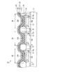
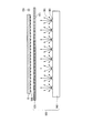
- FIG. 1 is a cross-sectional view showing a schematic configuration of an organic EL display device.
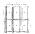
- FIG. 2 is a plan view showing a configuration of a pixel constituting the organic EL display device shown in FIG.
- FIG. 3 is a cross-sectional view of the TFT substrate constituting the organic EL display device taken along line 3-3 in FIG.
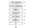
- FIG. 4 is a flowchart showing the manufacturing process of the organic EL display device in the order of steps.
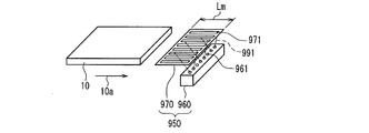
- FIG. 5 is a perspective view showing the basic concept of the new vapor deposition method.
- FIG. 6 is a front cross-sectional view of the vapor deposition apparatus shown in FIG. 5 as viewed along a direction parallel to the traveling direction of the substrate.
- FIG. 1 is a cross-sectional view showing a schematic configuration of an organic EL display device.
- FIG. 2 is a plan view showing a configuration of a pixel constituting the organic EL display device shown in FIG.
- FIG. 3 is a cross-sectional view of the
- FIG. 7 is a cross-sectional view for explaining the cause of blurring occurring at the edge of the coating in the new vapor deposition method of FIG.
- FIG. 8 is a perspective view showing the basic concept of a new vapor deposition method.
- FIG. 9 is a front sectional view of the vapor deposition apparatus shown in FIG. 8 as seen along a direction parallel to the traveling direction of the substrate.
- FIG. 10A is a cross-sectional view showing a film formed on a substrate in an ideal state in the new vapor deposition method
- FIG. 10B shows a difference in thermal expansion between the vapor deposition source and the control plate unit in the new vapor deposition method. It is sectional drawing which showed the film formed in the board
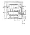
- FIG. 11 is a perspective view showing the main part of the vapor deposition apparatus according to Embodiment 1 of the present invention.
- FIG. 12 is a front cross-sectional view of the vapor deposition apparatus according to Embodiment 1 of the present invention viewed along the substrate scanning direction.
- FIG. 13 is a flowchart of a vapor deposition method using the vapor deposition apparatus according to Embodiment 1 of the present invention.
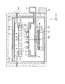
- FIG. 14 is a front cross-sectional view of the vapor deposition apparatus according to Embodiment 2 of the present invention viewed along the substrate scanning direction.
- FIG. 15: is front sectional drawing seen along the scanning direction of the board
- FIG. 16 is a flowchart of a vapor deposition method using the vapor deposition apparatus according to Embodiment 4 of the present invention.
- the vapor deposition method of the present invention is a vapor deposition method for forming a film with a predetermined pattern on a substrate, and includes a vapor deposition step of forming the film by adhering vapor deposition particles on the substrate.
- the vapor deposition step includes a vapor deposition source having a plurality of vapor deposition source openings for emitting the vapor deposition particles, a vapor deposition mask disposed between the plurality of vapor deposition source openings and the substrate, and a normal direction of the substrate.
- the substrate and the vapor deposition using a vapor deposition unit including a plurality of control plates arranged along a first direction orthogonal to each other, and comprising a control plate unit arranged between the vapor deposition source and the vapor deposition mask.
- One of the substrate and the vapor deposition unit is relatively relative to the other along a normal direction of the substrate and a second direction orthogonal to the first direction, with the mask being spaced apart by a certain distance.
- the vapor deposition method further includes a step of detecting a difference in thermal expansion amount in the first direction between the vapor deposition source and the control plate unit, and a step of correcting the difference in thermal expansion amount.
- the thermal expansion amount difference it is preferable to correct the thermal expansion amount difference by rotating the vapor deposition source in a plane parallel to the first direction and the second direction.
- the position shift in the first direction between the vapor deposition source opening and the control plate due to the difference in thermal expansion between the vapor deposition source and the control plate unit can be corrected by a simple method.
- the step of detecting the difference in thermal expansion and the step of correcting the difference in thermal expansion be performed before forming the coating film on the substrate. Thereby, it is possible to correct the positional deviation in the first direction between the vapor deposition source opening and the control plate caused by the difference in thermal expansion between the vapor deposition source and the control plate unit generated in the process of raising the temperature from room temperature to the vapor deposition temperature. .
- the step of detecting the difference in thermal expansion amount and the step of correcting the difference in thermal expansion amount may be performed while forming the film on the substrate. Accordingly, it is possible to correct the positional deviation in the first direction between the vapor deposition source opening and the control plate caused by the difference in thermal expansion between the vapor deposition source and the control plate unit generated by the temperature change during vapor deposition.
- the thermal expansion amount difference may be detected by observing the vapor deposition source and the control plate unit separately from different points other than the vapor deposition source and the control plate unit.
- the thermal expansion amount difference may be detected by simultaneously observing the vapor deposition source and the control plate unit from a common point other than the vapor deposition source and the control plate unit. Thereby, the thermal expansion amount difference can be detected with higher accuracy. In addition, the number of devices for detecting the difference in thermal expansion can be reduced.
- the thermal expansion amount difference may be detected by observing one of the vapor deposition source and the control plate unit from the other. Thereby, the calculation process of the thermal expansion amount difference can be simplified. In addition, the number of devices for detecting the difference in thermal expansion can be reduced.
- the vapor deposition method of the present invention further includes a step of detecting a positional deviation amount in the first direction between the vapor deposition source and the control plate unit and a step of correcting the positional deviation amount. Thereby, the amount of positional deviation in the first direction between the vapor deposition source opening and the control plate can be further reduced.
- the step of detecting the amount of positional deviation and the step of correcting the amount of positional deviation may be performed while forming the film on the substrate. Thereby, the position shift between the vapor deposition source and the control plate unit generated by the temperature change during vapor deposition can be corrected.
- the position deviation amount may be detected by separately observing the vapor deposition source and the control plate unit from different points other than the vapor deposition source and the control plate unit.
- the positional deviation amount may be detected by simultaneously observing the vapor deposition source and the control plate unit from a common point other than the vapor deposition source and the control plate unit. Thereby, it is possible to detect the positional deviation amount with higher accuracy. In addition, the number of devices for detecting the positional deviation amount can be reduced.
- the positional deviation amount may be detected by observing one of the vapor deposition source and the control plate unit from the other. Thereby, it is possible to simplify the calculation processing of the positional deviation amount. In addition, the number of devices for detecting the positional deviation amount can be reduced.
- the coating film is a light emitting layer of an organic EL element. Therefore, it is possible to provide an organic EL display device which is excellent in reliability and display quality and can be enlarged.
- a vapor deposition apparatus is a vapor deposition apparatus that forms a film with a predetermined pattern on a substrate, the vapor deposition source having a plurality of vapor deposition source openings that emit vapor deposition particles for forming the film, and the plurality of vapor depositions
- a deposition mask disposed between a source opening and the substrate, and a plurality of control plates disposed along a first direction orthogonal to a normal direction of the substrate, the deposition source and the deposition mask;
- a moving mechanism for moving one of the substrate and the vapor deposition unit relative to the other along the line, and a means for detecting a difference in thermal expansion in the first direction between the vapor deposition source and the control plate unit And the thermal expansion And means for correcting the amount difference.
- the means for correcting the difference in thermal expansion includes a rotation drive mechanism that rotates the vapor deposition source in a plane parallel to the first direction and the second direction.
- the vapor deposition apparatus of the present invention further includes means for detecting a positional deviation amount in the first direction between the vapor deposition source and the control plate unit, and means for correcting the positional deviation amount. Thereby, the amount of positional deviation in the first direction between the vapor deposition source opening and the control plate can be further reduced.
- the means for correcting the positional deviation amount includes a linear drive mechanism that moves the vapor deposition source in the first direction.
- the position shift in the first direction between the vapor deposition source and the control plate unit can be corrected by a simple method.
- the means for detecting the positional deviation amount includes a member common to the means for correcting the difference in thermal expansion.
- the organic EL display device of this example is a bottom emission type in which light is extracted from the TFT substrate side, and controls light emission of pixels (sub-pixels) composed of red (R), green (G), and blue (B) colors.
- This is an organic EL display device that performs full-color image display.
- FIG. 1 is a cross-sectional view showing a schematic configuration of an organic EL display device.
- FIG. 2 is a plan view showing a configuration of a pixel constituting the organic EL display device shown in FIG.
- FIG. 3 is a cross-sectional view of the TFT substrate constituting the organic EL display device taken along line 3-3 in FIG.
- the organic EL display device 1 includes an organic EL element 20, an adhesive layer 30, and a sealing substrate 40 connected to a TFT 12 on a TFT substrate 10 on which a TFT 12 (see FIG. 3) is provided. It has the structure provided in order.
- the center of the organic EL display device 1 is a display area 19 for displaying an image, and an organic EL element 20 is disposed in the display area 19.
- the organic EL element 20 is sealed between the pair of substrates 10 and 40 by bonding the TFT substrate 10 on which the organic EL element 20 is laminated to the sealing substrate 40 using the adhesive layer 30. As described above, since the organic EL element 20 is sealed between the TFT substrate 10 and the sealing substrate 40, entry of oxygen and moisture into the organic EL element 20 from the outside is prevented.
- the TFT substrate 10 includes a transparent insulating substrate 11 such as a glass substrate as a supporting substrate.
- the insulating substrate 11 does not need to be transparent.
- a plurality of wirings 14 including a plurality of gate lines laid in the horizontal direction and a plurality of signal lines laid in the vertical direction and intersecting the gate lines are provided. It has been.
- a gate line driving circuit (not shown) for driving the gate line is connected to the gate line
- a signal line driving circuit (not shown) for driving the signal line is connected to the signal line.
- sub-pixels 2R, 2G, and 2B made of organic EL elements 20 of red (R), green (G), and blue (B) colors are provided in each region surrounded by the wirings 14, respectively. They are arranged in a matrix.
- the sub-pixel 2R emits red light
- the sub-pixel 2G emits green light
- the sub-pixel 2B emits blue light.
- Sub-pixels of the same color are arranged in the column direction (vertical direction in FIG. 2), and repeating units composed of sub-pixels 2R, 2G, and 2B are repeatedly arranged in the row direction (left-right direction in FIG. 2).
- the sub-pixels 2R, 2G, and 2B constituting the repeating unit in the row direction constitute the pixel 2 (that is, one pixel).
- Each sub-pixel 2R, 2G, 2B includes a light-emitting layer 23R, 23G, 23B responsible for light emission of each color.
- the light emitting layers 23R, 23G, and 23B extend in a stripe shape in the column direction (vertical direction in FIG. 2).
- the configuration of the TFT substrate 10 will be described.
- the TFT substrate 10 is formed on a transparent insulating substrate 11 such as a glass substrate, a TFT 12 (switching element), a wiring 14, an interlayer film 13 (interlayer insulating film, planarizing film), an edge cover 15, and the like. Is provided.
- the TFT 12 functions as a switching element that controls the light emission of the sub-pixels 2R, 2G, and 2B, and is provided for each of the sub-pixels 2R, 2G, and 2B.
- the TFT 12 is connected to the wiring 14.
- the interlayer film 13 also functions as a planarizing film, and is laminated on the entire surface of the display region 19 on the insulating substrate 11 so as to cover the TFT 12 and the wiring 14.
- a first electrode 21 is formed on the interlayer film 13.
- the first electrode 21 is electrically connected to the TFT 12 through a contact hole 13 a formed in the interlayer film 13.
- the edge cover 15 is formed on the interlayer film 13 so as to cover the pattern end of the first electrode 21.
- the edge cover 15 has a short circuit between the first electrode 21 and the second electrode 26 constituting the organic EL element 20 because the organic EL layer 27 is thinned or electric field concentration occurs at the pattern end of the first electrode 21. This is an insulating layer for preventing this.
- the edge cover 15 is provided with openings 15R, 15G, and 15B for each of the sub-pixels 2R, 2G, and 2B.
- the openings 15R, 15G, and 15B of the edge cover 15 serve as light emitting areas of the sub-pixels 2R, 2G, and 2B.
- each of the sub-pixels 2R, 2G, 2B is partitioned by the edge cover 15 having an insulating property.
- the edge cover 15 also functions as an element isolation film.
- the organic EL element 20 will be described.
- the organic EL element 20 is a light emitting element that can emit light with high luminance by low voltage direct current drive, and includes a first electrode 21, an organic EL layer 27, and a second electrode 26 in this order.
- the first electrode 21 is a layer having a function of injecting (supplying) holes into the organic EL layer 27. As described above, the first electrode 21 is connected to the TFT 12 via the contact hole 13a.
- the organic EL layer 27 includes a hole injection layer / hole transport layer 22, light emitting layers 23 ⁇ / b> R, 23 ⁇ / b> G, between the first electrode 21 and the second electrode 26 from the first electrode 21 side. 23B, the electron transport layer 24, and the electron injection layer 25 are provided in this order.
- the first electrode 21 is an anode and the second electrode 26 is a cathode.
- the first electrode 21 may be a cathode and the second electrode 26 may be an anode.
- the organic EL layer 27 is configured. The order of each layer is reversed.
- the hole injection layer / hole transport layer 22 has both a function as a hole injection layer and a function as a hole transport layer.
- the hole injection layer is a layer having a function of increasing hole injection efficiency into the organic EL layer 27.
- the hole transport layer is a layer having a function of improving the efficiency of transporting holes to the light emitting layers 23R, 23G, and 23B.
- the hole injection layer / hole transport layer 22 is uniformly formed on the entire surface of the display region 19 in the TFT substrate 10 so as to cover the first electrode 21 and the edge cover 15.
- the hole injection layer / hole transport layer 22 in which the hole injection layer and the hole transport layer are integrated is provided.
- the hole transport layer may be formed as a layer independent of each other.
- the light emitting layers 23R, 23G, and 23B correspond to the columns of the sub-pixels 2R, 2G, and 2B so as to cover the openings 15R, 15G, and 15B of the edge cover 15, respectively. Is formed.
- the light emitting layers 23R, 23G, and 23B are layers having a function of emitting light by recombining holes injected from the first electrode 21 side and electrons injected from the second electrode 26 side. .
- Each of the light emitting layers 23R, 23G, and 23B includes a material having high light emission efficiency such as a low molecular fluorescent dye or a metal complex.
- the electron transport layer 24 is a layer having a function of increasing the electron transport efficiency from the second electrode 26 to the light emitting layers 23R, 23G, and 23B.
- the electron injection layer 25 is a layer having a function of increasing the efficiency of electron injection from the second electrode 26 to the organic EL layer 27.
- the electron transport layer 24 is formed on the light emitting layers 23R, 23G, 23B and the hole injection / hole transport layer 22 so as to cover the light emitting layers 23R, 23G, 23B and the hole injection / hole transport layer 22. It is uniformly formed over the entire surface of the display area 19 in the substrate 10.
- the electron injection layer 25 is uniformly formed on the entire surface of the display region 19 in the TFT substrate 10 on the electron transport layer 24 so as to cover the electron transport layer 24.
- the electron transport layer 24 and the electron injection layer 25 are provided as independent layers.
- the present invention is not limited to this, and a single layer in which both are integrated (that is, an electron) It may be provided as a transport layer / electron injection layer).
- the second electrode 26 is a layer having a function of injecting electrons into the organic EL layer 27.
- the second electrode 26 is formed uniformly over the entire surface of the display region 19 in the TFT substrate 10 on the electron injection layer 25 so as to cover the electron injection layer 25.
- the organic layers other than the light emitting layers 23R, 23G, and 23B are not essential as the organic EL layer 27, and may be selected according to the required characteristics of the organic EL element 20.
- the organic EL layer 27 may further include a carrier blocking layer as necessary. For example, by adding a hole blocking layer as a carrier blocking layer between the light emitting layers 23R, 23G, and 23B and the electron transport layer 24, holes are prevented from passing through the electron transport layer 24, and the light emission efficiency is improved. can do.
- FIG. 4 is a flowchart showing the manufacturing process of the organic EL display device 1 in the order of steps.
- the manufacturing method of the organic EL display device 1 includes, for example, a TFT substrate / first electrode manufacturing step S1, a hole injection layer / hole transport layer forming step S2, and light emission.
- a layer forming step S3, an electron transporting layer forming step S4, an electron injecting layer forming step S5, a second electrode forming step S6, and a sealing step S7 are provided in this order.
- the first electrode 21 is an anode and the second electrode 26 is a cathode.
- the organic EL the order of layer stacking is reversed from the description below.
- the materials constituting the first electrode 21 and the second electrode 26 are also reversed from the following description.
- the TFT 12 and the wiring 14 are formed on the insulating substrate 11 by a known method.
- the insulating substrate 11 for example, a transparent glass substrate or a plastic substrate can be used.
- a rectangular glass plate having a thickness of about 1 mm and a vertical and horizontal dimension of 500 ⁇ 400 mm can be used as the insulating substrate 11.
- a photosensitive resin is applied on the insulating substrate 11 so as to cover the TFT 12 and the wiring 14, and the interlayer film 13 is formed by patterning using a photolithography technique.
- a material of the interlayer film 13 for example, an insulating material such as an acrylic resin or a polyimide resin can be used.
- the polyimide resin is generally not transparent but colored. For this reason, when the bottom emission type organic EL display device 1 as shown in FIG. 3 is manufactured, it is preferable to use a transparent resin such as an acrylic resin as the interlayer film 13.
- the thickness of the interlayer film 13 is not particularly limited as long as the step on the upper surface of the TFT 12 can be eliminated. In one embodiment, the interlayer film 13 having a thickness of about 2 ⁇ m can be formed using an acrylic resin.
- a contact hole 13 a for electrically connecting the first electrode 21 to the TFT 12 is formed in the interlayer film 13.
- the first electrode 21 is formed on the interlayer film 13. That is, a conductive film (electrode film) is formed on the interlayer film 13. Next, after applying a photoresist on the conductive film and performing patterning using a photolithography technique, the conductive film is etched using ferric chloride as an etchant. Thereafter, the photoresist is stripped using a resist stripping solution, and substrate cleaning is further performed. Thereby, a matrix-like first electrode 21 is obtained on the interlayer film 13.
- transparent conductive materials such as ITO (Indium (Tin Oxide), IZO (Indium Zinc Oxide), gallium-doped zinc oxide (GZO), Metal materials such as gold (Au), nickel (Ni), and platinum (Pt) can also be used.
- a sputtering method As a method for laminating the conductive film, a sputtering method, a vacuum deposition method, a CVD (chemical vapor deposition) method, a plasma CVD method, a printing method, or the like can be used.
- a vacuum deposition method As a method for laminating the conductive film, a sputtering method, a vacuum deposition method, a CVD (chemical vapor deposition) method, a plasma CVD method, a printing method, or the like can be used.
- CVD chemical vapor deposition
- the first electrode 21 having a thickness of about 100 nm can be formed by sputtering using ITO.
- the edge cover 15 having a predetermined pattern is formed.
- the edge cover 15 can use, for example, the same insulating material as that of the interlayer film 13 and can be patterned by the same method as that of the interlayer film 13.
- the edge cover 15 having a thickness of about 1 ⁇ m can be formed using acrylic resin.
- the TFT substrate 10 and the first electrode 21 are manufactured (step S1).
- the TFT substrate 10 that has undergone the step S1 is subjected to a vacuum baking process for dehydration, and further subjected to an oxygen plasma process for cleaning the surface of the first electrode 21.
- a hole injection layer and a hole transport layer are formed on the entire surface of the display region 19 of the TFT substrate 10 on the TFT substrate 10 by vapor deposition. (S2).
- an open mask having the entire display area 19 opened is closely fixed to the TFT substrate 10 and the TFT substrate 10 and the open mask are rotated together.
- the material of the transport layer is deposited on the entire surface of the display area 19 of the TFT substrate 10.
- the hole injection layer and the hole transport layer may be integrated as described above, or may be layers independent of each other.
- the thickness of the layer is, for example, 10 to 100 nm per layer.
- Examples of the material for the hole injection layer and the hole transport layer include benzine, styrylamine, triphenylamine, porphyrin, triazole, imidazole, oxadiazole, polyarylalkane, phenylenediamine, arylamine, oxazole, anthracene, and fluorenone. , Hydrazone, stilbene, triphenylene, azatriphenylene, and derivatives thereof, polysilane compounds, vinylcarbazole compounds, thiophene compounds, aniline compounds, etc., heterocyclic or chain conjugated monomers, oligomers, or polymers Etc.
- 4,4′-bis [N- (1-naphthyl) -N-phenylamino] biphenyl ( ⁇ -NPD) is used to form a hole injection layer / hole transport layer 22 having a thickness of 30 nm. Can be formed.
- the light emitting layers 23R, 23G, and 23B are formed in a stripe shape on the hole injection / hole transport layer 22 so as to cover the openings 15R, 15G, and 15B of the edge cover 15 (S3).
- the light emitting layers 23R, 23G, and 23B are vapor-deposited so that a predetermined region is separately applied for each color of red, green, and blue (separate vapor deposition).
- a material having high luminous efficiency such as a low molecular fluorescent dye or a metal complex is used.
- a material having high luminous efficiency such as a low molecular fluorescent dye or a metal complex.
- the thickness of the light emitting layers 23R, 23G, and 23B can be set to 10 to 100 nm, for example.
- the vapor deposition method and vapor deposition apparatus of the present invention can be used particularly suitably for the separate vapor deposition of the light emitting layers 23R, 23G, and 23B. Details of the method of forming the light emitting layers 23R, 23G, and 23B using the present invention will be described later.
- the electron transport layer 24 is formed on the entire surface of the display region 19 of the TFT substrate 10 by vapor deposition so as to cover the hole injection layer / hole transport layer 22 and the light emitting layers 23R, 23G, and 23B (S4).
- the electron transport layer 24 can be formed by the same method as in the hole injection layer / hole transport layer forming step S2.
- an electron injection layer 25 is formed on the entire surface of the display region 19 of the TFT substrate 10 by vapor deposition so as to cover the electron transport layer 24 (S5).
- the electron injection layer 25 can be formed by the same method as in the hole injection layer / hole transport layer forming step S2.
- Examples of the material for the electron transport layer 24 and the electron injection layer 25 include quinoline, perylene, phenanthroline, bisstyryl, pyrazine, triazole, oxazole, oxadiazole, fluorenone, and derivatives and metal complexes thereof, LiF (lithium fluoride). Etc. can be used.
- the electron transport layer 24 and the electron injection layer 25 may be formed as an integrated single layer or may be formed as independent layers.
- the thickness of each layer is, for example, 1 to 100 nm.
- the total thickness of the electron transport layer 24 and the electron injection layer 25 is, for example, 20 to 200 nm.
- Alq tris (8-hydroxyquinoline) aluminum
- LiF lithium fluoride
- the second electrode 26 is formed on the entire surface of the display region 19 of the TFT substrate 10 by vapor deposition so as to cover the electron injection layer 25 (S6).
- the second electrode 26 can be formed by the same method as in the hole injection layer / hole transport layer forming step S2 described above.
- a material (electrode material) of the second electrode 26 a metal having a small work function is preferably used. Examples of such electrode materials include magnesium alloys (MgAg, etc.), aluminum alloys (AlLi, AlCa, AlMg, etc.), metallic calcium, and the like.
- the thickness of the second electrode 26 is, for example, 50 to 100 nm. In one embodiment, the second electrode 26 having a thickness of 50 nm can be formed using aluminum.
- a protective film may be further provided on the second electrode 26 so as to cover the second electrode 26 and prevent oxygen and moisture from entering the organic EL element 20 from the outside.
- a material for the protective film an insulating or conductive material can be used, and examples thereof include silicon nitride and silicon oxide.
- the thickness of the protective film is, for example, 100 to 1000 nm.
- the organic EL element 20 including the first electrode 21, the organic EL layer 27, and the second electrode 26 can be formed on the TFT substrate 10.
- the TFT substrate 10 on which the organic EL element 20 is formed and the sealing substrate 40 are bonded together with an adhesive layer 30 to encapsulate the organic EL element 20.
- an insulating substrate such as a glass substrate or a plastic substrate having a thickness of 0.4 to 1.1 mm can be used.
- the organic EL display device 1 is obtained.
- step S3 of forming the light emitting layers 23R, 23G, and 23B by separate deposition will be described.
- New vapor deposition method As a method for separately depositing the light emitting layers 23R, 23G, and 23B, the present inventors replaced the evaporation method in which a mask having the same size as the substrate is fixed to the substrate at the time of deposition, as in Patent Documents 1 and 2.
- a new vapor deposition method (hereinafter referred to as “new vapor deposition method”) in which vapor deposition is performed while moving the substrate relative to the vapor deposition source and the vapor deposition mask was studied.
- FIG. 5 is a perspective view showing the basic concept of the new vapor deposition method.
- the vapor deposition source 960 and the vapor deposition mask 970 constitute a vapor deposition unit 950.
- the relative position of the vapor deposition source 960 and the vapor deposition mask 970 is constant.
- the substrate 10 moves in one direction 10a at a constant speed on the opposite side of the vapor deposition mask 970 from the vapor deposition source 960.
- a plurality of vapor deposition source openings 961 each emitting vapor deposition particles 991 are formed on the upper surface of the vapor deposition source 960, and a plurality of mask openings 971 are formed in the vapor deposition mask 970.
- the vapor deposition particles 991 emitted from the vapor deposition source opening 961 pass through the mask opening 971 and adhere to the substrate 10.
- the dimension Lm of the deposition mask 970 in the moving direction 10a of the substrate 10 can be set regardless of the dimension of the substrate 10 in the same direction. Therefore, an evaporation mask 970 smaller than the substrate 10 can be used. For this reason, since it is not necessary to enlarge the vapor deposition mask 970 even if the board
- FIG. 6 is a front view of the vapor deposition apparatus of FIG. 5 as viewed along a direction parallel to the moving direction 10a of the substrate 10.
- a plurality of vapor deposition source openings 961 and a plurality of mask openings 971 are arranged in the left-right direction on the paper surface of FIG.
- the vapor deposition particles 991 are emitted from each vapor deposition source opening 961 with a certain spread (directivity). That is, in FIG. 6, the number of vapor deposition particles 991 emitted from the vapor deposition source opening 961 is the largest in the direction directly above the vapor deposition source opening 961, and as the angle (emission angle) formed with respect to the direct upward direction increases. Gradually decreases.
- Each vapor-deposited particle 991 emitted from the vapor deposition source opening 961 goes straight in the respective emission direction.
- the flow of the vapor deposition particles 991 emitted from the vapor deposition source opening 961 is conceptually indicated by arrows. Therefore, most of the vapor deposition particles 991 emitted from the vapor deposition source opening 961 located immediately below each mask opening 971 fly, but the present invention is not limited to this, and is emitted from the vapor deposition source opening 961 located obliquely below. The vapor deposition particles 991 also fly.
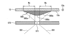
- FIG. 7 is a cross-sectional view of the coating film 990 formed on the substrate 10 by the vapor deposition particles 991 that have passed through a certain mask opening 971, as seen in a direction parallel to the moving direction 10a of the substrate 10 as in FIG. .
- the vapor deposition particles 991 flying from various directions pass through the mask opening 971.
- the number of the vapor deposition particles 991 reaching the vapor deposition surface 10e of the substrate 10 is the largest in the region directly above the mask opening 971, and gradually decreases with increasing distance from the area. Therefore, as shown in FIG.
- a coating main portion 990 c having a thick and substantially constant thickness is formed on the deposition surface 10 e of the substrate 10 in a region where the mask opening 971 is projected onto the substrate 10 in the directly upward direction.
- a blurred portion 990e is formed which becomes gradually thinner as it becomes farther from the coating main portion 990c.
- the blurred portion 990e causes the edge of the coating film 990 to be blurred.
- the distance between the vapor deposition mask 970 and the substrate 10 may be reduced. However, since it is necessary to move the substrate 10 relative to the vapor deposition mask 970 in the new vapor deposition method, the distance between the vapor deposition mask 970 and the substrate 10 cannot be made zero.
- the aperture width of the pixel (meaning the sub-pixels 2R, 2G, and 2B in FIG. 2) is set so that the blurred portion 990e does not reach the adjacent light emitting layer regions of different colors. It is necessary to increase the non-light-emitting region by narrowing or increasing the pixel pitch. However, when the aperture width of the pixel is narrowed, the light emitting area becomes small and the luminance is lowered.
- the new vapor deposition method shown in FIG. 5 has a feature that separate vapor deposition can be performed even on a large substrate, but a blurred portion 990e is generated at the edge of the coating (deposition film). In addition, it is difficult to reduce the width We of the blurred portion 990e.
- New deposition method As a separate vapor deposition method that solves the above-described problems of the new vapor deposition method shown in FIGS. 5 and 6, the present inventors have provided a vapor deposition method in which a plurality of control plates are disposed between a vapor deposition source and a vapor deposition mask ( Hereinafter, “new deposition method” was examined.
- FIG. 8 is a perspective view showing the basic concept of a new vapor deposition method.
- FIG. 9 is a front sectional view of the vapor deposition apparatus shown in FIG. 8 as seen along a direction parallel to the traveling direction of the substrate.
- the same members as those shown in FIGS. 5 and 6 are denoted by the same reference numerals, and description thereof is omitted.
- the horizontal axis along the width direction of the substrate 10 is the X axis
- the horizontal axis perpendicular to the X axis is the Y axis
- the vertical axis perpendicular to the X axis and the Y axis is the Z axis.
- the XYZ rectangular coordinate system to be set is set.
- the Y axis is parallel to the moving direction 10 a of the substrate 10
- the Z axis is parallel to the normal direction of the deposition surface 10 e of the substrate 10.
- a control plate unit 980 having a plurality of control plates 981 is disposed between the vapor deposition source 960 and the vapor deposition mask 970.
- the main surface (surface having the largest area) of each control plate 981 is parallel to the YZ plane.
- the plurality of control plates 981 are arranged at a constant pitch in parallel with the arrangement direction of the plurality of vapor deposition source openings 961 (that is, the X-axis direction).
- the plurality of control plates 981 are, for example, welded to a frame-shaped holding body 985 configured by a pair of first holding members 986 parallel to the X-axis direction and a pair of second holding members 987 parallel to the Y-axis direction. Are held together in a way.
- control plate 981 The operation of the control plate 981 will be described.
- control space 982 the vapor deposition particles 991
- the “incident angle” with respect to the mask opening 971 is defined as an angle formed by the flying direction of the vapor deposition particles 991 with respect to the Z axis in the projection view on the XZ plane.
- the directivity of the vapor deposition particles 991 in the X-axis direction can be improved by using the plurality of control plates 981. Accordingly, the width We of the blurred portion 990e can be reduced.
- the plurality of control plates 981 are parallel to the YZ plane, even the vapor deposition particles 991 having a large Y-axis direction component of the velocity vector are not captured by the control plate 981. Therefore, the use efficiency of the vapor deposition material and the decrease in the vapor deposition rate due to the use of the plurality of control plates 981 are slight.
- the vapor deposition source 960 needs to be maintained at a predetermined high temperature during vapor deposition in order to release the vapor deposition particles 991 from the vapor deposition source opening 961. Accordingly, the vapor deposition source 960 is thermally expanded in the process of raising the temperature from the normal temperature before the vapor deposition is started to the high temperature during the vapor deposition.
- control plate unit 980, the vapor deposition mask 970, and the like disposed in the vicinity of the vapor deposition source 960 are heated by the radiant heat from the vapor deposition source 960 and thermally expanded.
- FIG. 10A is a cross-sectional view showing the coating film 990 formed on the substrate 10 in an ideal state where no difference in thermal expansion occurs between the vapor deposition source 960 and its peripheral members.
- one vapor deposition source opening 961 is arranged for one control space 982, and the vapor deposition source opening 961 is arranged at the center position of the pair of control plates 981 in the X-axis direction.
- the vapor deposition particles 991 emitted from the vapor deposition source opening 961 the vapor deposition particles 991 that have passed through the control space 982 and the mask opening 971 in this order adhere to the substrate 10 and form a coating film 990.
- FIG. 10B is a cross-sectional view showing the coating film 990 formed on the substrate 10 in a state where a difference in thermal expansion occurs between the vapor deposition source 960, the control plate unit 980, and the vapor deposition mask 970.
- the vapor deposition source 960 is thermally expanded, whereas the control plate unit 980 and the vapor deposition mask 970 are not substantially thermally expanded.
- the deposition source opening 961 is displaced in the right direction with respect to the control plate 981 and the deposition mask 970.
- the deposition source opening 961 is displaced relative to the control plate 981 and the deposition mask 970, so that the position of the coating film 990 formed on the substrate 10 is relative to the ideal position 990 ′ shown in FIG. 10A. Shift the position to the left.
- the coating 990 is displaced due to the relative displacement of the deposition source opening 61 because the deposition source opening 961 that emits the deposition particles 991 incident on the respective mask openings 971. This is because the control plate 981 is selected.
- the distance between the vapor deposition mask 970 and the substrate 10 may be reduced.
- the interval between the vapor deposition mask 970 and the substrate 10 cannot be made zero.
- the aperture width of the pixels (meaning the sub-pixels 2R, 2G, and 2B in FIG. 2) is reduced, or the pitch of the pixels is increased to increase the non-light emitting area.
- the aperture width of the pixel is narrowed, the light emitting area becomes small and the luminance is lowered.
- the current density is increased in order to obtain the necessary luminance, the life of the organic EL element is shortened or is easily damaged, and the reliability is lowered.
- the pixel pitch is increased, high-definition display cannot be realized and display quality is deteriorated.
- the inventors of the present invention have intensively studied to solve the above problems of the vapor deposition method, and have completed the present invention.
- the preferred embodiments of the present invention will be described below.
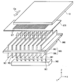
- FIG. 11 is a perspective view showing the main part of the vapor deposition apparatus according to Embodiment 1 of the present invention.
- the horizontal axis along the width direction (first direction) of the substrate 10 is the X axis
- the horizontal axis perpendicular to the X axis is the Y axis
- the vertical direction perpendicular to the X axis and the Y axis is set.
- An XYZ orthogonal coordinate system having the Z axis as an axis is set.
- the Z axis is parallel to the normal direction of the deposition surface of the substrate 10.
- the side of the arrow in the Z-axis direction (the upper side of the paper in FIG. 11) is referred to as the “upper side”.
- a vapor deposition mask 70 is arranged facing the vapor deposition source 60 in the Z-axis direction.
- the vapor deposition source 60 includes a plurality of vapor deposition source openings 61 on the upper surface (that is, the surface facing the vapor deposition mask 70).
- the plurality of vapor deposition source openings 61 are arranged at a constant pitch along a straight line substantially parallel to the X-axis direction.
- Each vapor deposition source opening 61 has a nozzle shape opened upward in parallel with the Z axis, and emits vapor deposition particles 91 serving as a material of the light emitting layer toward the vapor deposition mask 70.
- the vapor deposition mask 70 is a plate-like object whose main surface (surface having the largest area) is parallel to the XY plane, and a plurality of mask openings 71 are formed at different positions in the X-axis direction along the X-axis direction. Yes.
- the opening shape of each mask opening 71 has a slot shape parallel to the Y axis, but the present invention is not limited to this.
- the shape and dimensions of all the mask openings 71 may be the same or different.
- the pitch of the mask openings 71 in the X-axis direction may be constant or different.
- a control plate unit 80 is disposed between the vapor deposition source opening 61 and the vapor deposition mask 70.
- the control plate unit 80 includes a plurality of control plates 81 arranged at a constant pitch along the X-axis direction.
- the plurality of control plates 81 are thin plates having the same dimensions, and their main surfaces (surfaces having the largest areas) are parallel to the Y axis and the Z axis.
- a space between the control plates 81 adjacent in the X-axis direction is a control space 82 through which the vapor deposition particles 91 pass.
- the number of the vapor deposition source openings 61 and the control spaces 82 is four, but the present invention is not limited to this and may be more or less. Moreover, the vapor deposition source openings 61 and the control spaces 82 do not have to be the same number, and either one may be larger than the other.
- control plate unit 80 is formed by forming a rectangular parallelepiped through-hole penetrating in the Z-axis direction at a constant pitch in the X-axis direction.
- Each through hole serves as a control space 82, and a partition between adjacent through holes serves as a control plate 81.
- the manufacturing method of the control unit 80 is not limited to this.
- a plurality of control plates 81 having the same dimensions separately created may be fixed to a substantially rectangular frame-shaped holding body at a constant pitch by welding or the like.
- a shutter 95 made of a thin plate is disposed with its main surface parallel to the XY plane.
- the shutter 95 can reciprocate between a position between the vapor deposition source 60 and the control plate unit 80 and a position retracted from this position.
- a state in which the shutter 95 is positioned between the vapor deposition source 60 and the control plate unit 80 is referred to as a state in which the shutter 95 is closed. In this state, vapor deposition particles 91 emitted from the vapor deposition source opening 61 enter the control space 82. Cannot enter.
- a state in which the shutter 95 is retracted from between the vapor deposition source 60 and the control plate unit 80 is referred to as a state in which the shutter 95 is opened. In this state, the vapor deposition particles 91 emitted from the vapor deposition source opening 61 enter the control space 82. Incident.
- the vapor deposition source opening 61 and the plurality of control plates 81 are separated from each other in the Z-axis direction, and the plurality of control plates 81 and the vapor deposition mask 70 are separated from each other in the Z-axis direction.
- the relative positions of the vapor deposition source 60, the control plate unit 80, and the vapor deposition mask 70 are constant at least during the period in which the separate vapor deposition is performed, except for the position adjustment of the vapor deposition source 60 for performing correction described later.
- the vapor deposition source 60, the shutter 95, the control plate unit 80, and the vapor deposition mask 70 constitute a vapor deposition unit 50.
- the substrate 10 is moved in the Y-axis direction (second direction) 10a at a constant speed in a state where the opposite side of the vapor deposition source 60 from the vapor deposition mask 70 is separated from the vapor deposition mask 70 by a predetermined interval by a moving mechanism (not shown). Scanned (moved).
- the shutter 95 When the shutter 95 is opened in a state where the vapor deposition particles 91 are released from the vapor deposition source opening 61, the vapor deposition particles 91 sequentially pass through the control space 82 of the control plate unit 80 and the mask opening 71 of the vapor deposition mask 70.
- the vapor deposition particles 91 adhere to the vapor deposition surface (that is, the surface of the substrate 10 facing the vapor deposition mask 70) 10e that travels in the Y-axis direction to form a film 90 (see FIG. 12 described later).
- the film 90 has a stripe shape extending in the Y-axis direction.
- the vapor deposition particles 91 forming the coating film 90 always pass through the control space 82 and the mask opening 71.
- the control plate unit 80 and the vapor deposition mask 70 are designed so that the vapor deposition particles 91 emitted from the vapor deposition source opening 61 do not reach the vapor deposition surface 10e of the substrate 10 without passing through the control space 82 and the mask opening 71. Further, if necessary, an adhesion prevention plate or the like (not shown) that prevents the vapor deposition particles 91 from flying may be installed.
- a striped film corresponding to each color of red, green, and blue on the vapor deposition surface 10e of the substrate 10 90 (that is, the light emitting layers 23R, 23G, and 23B) can be formed.
- the control plate 81 is projected onto the XZ plane by colliding and adhering vapor deposition particles 91 having a large X-axis direction component of the velocity vector.
- the incident angle of the vapor deposition particles 91 incident on the mask opening 71 is limited.
- the “incident angle” with respect to the mask opening 71 is defined as an angle formed by the flying direction of the vapor deposition particles 91 with respect to the Z axis in the projection view on the XZ plane.
- the vapor deposition particles 91 passing through the mask opening 71 at a large incident angle are reduced. Accordingly, the width We of the blurred portion 990e shown in FIG.
- the thickness gradually decreasing portion 990e is substantially not generated, so that the occurrence of blurring at the edges on both sides of the striped film 90 is greatly suppressed. Is done.
- the organic EL display device it is not necessary to increase the width of the non-light emitting region between the light emitting regions so that color mixing does not occur. Therefore, high-luminance and high-definition display can be realized.
- a long life can be realized and the reliability is improved.
- FIG. 12 is a front cross-sectional view of the vapor deposition apparatus of Embodiment 1 as viewed along a direction perpendicular to the width direction of the substrate 10. The detailed structure of the vapor deposition apparatus of the first embodiment will be described with reference to FIG.
- the vapor deposition source 60 is installed on the frame bottom plate 111 via a linear drive mechanism 121 and a rotary drive mechanism 125.
- the linear drive mechanism 121 moves the rotational drive mechanism 125 and the vapor deposition source 60 mounted thereon in the X-axis direction, and adjusts the position in the X-axis direction.
- the configuration of the linear drive mechanism 121 is not particularly limited, and a known uniaxial positioning device such as a linear motor can be used.
- the rotation drive mechanism 125 rotates the vapor deposition source 60 mounted thereon in a plane parallel to the XY plane, and adjusts the rotational position of the vapor deposition source 60 in the plane.
- the rotation center axis 125a of the rotation drive mechanism 125 is parallel to the Z axis, and preferably, a central position between the evaporation source openings 61 at both ends in the X-axis direction among the plurality of evaporation source openings 61 formed in the evaporation source 60. It is preferable to pass through this position (referred to as the center position of the vapor deposition source 60 in the X-axis direction).
- the rotation drive mechanism 125 includes a large gear 126 that can rotate around the rotation center shaft 125a, a small gear 127 that meshes with the large gear 126, and a stepping motor 128 that rotates the small gear 127.
- the vapor deposition source 60 is mounted on the large gear 126.
- the configuration of the rotational drive mechanism 125 is not limited to this, and a known rotational positioning device can be used.
- a heater 63 is attached around the vapor deposition source 60 in order to heat and maintain the vapor deposition source 60 at a predetermined temperature and prevent the vapor deposition particles 91 from adhering to the vapor deposition source 60.
- the temperature of the vapor deposition source 60 at the time of vapor deposition is suitably set according to the kind of vapor deposition particle 91, etc., it is about 400 degreeC, for example.
- a vapor deposition particle generator 65 is disposed outside the chamber 101.
- the vapor deposition particle generator 65 heats and vaporizes the vapor deposition material, and sends the vapor of the generated vapor deposition material to the vapor deposition source 60 in the chamber 101 through a pipe.
- a flexible joint 67 for allowing a change in the position of the vapor deposition source 60 is installed.
- the vapor of the vapor deposition material is emitted as vapor deposition particles 91 from the vapor deposition source opening 61 of the vapor deposition source 60.
- the vapor deposition particle generator 65 may have a function of separately heating and evaporating two or more types of vapor deposition materials, mixing the vapors, and sending the vapors to the vapor deposition source 60.
- the shutter 95 is held by the frame side plate 112 via a linear drive mechanism (not shown) that can reciprocate the shutter 95 in the Y-axis direction.
- the control plate unit 80 is held by an arm extending from the frame side plate 112.
- First alignment marks 201 are formed on both ends of the vapor deposition source 60 in the X-axis direction.
- a first recognition unit 211 that recognizes the position of the first alignment mark 201 faces each alignment mark 201 in the Z-axis direction.
- second alignment marks 202 are formed on both ends of the control plate unit 80 in the X-axis direction.
- a second recognition unit 212 that recognizes the position of the second alignment mark 202 faces each alignment mark 202.
- the 1st and 2nd recognition parts 211 and 212 are hold
- the configuration of the first and second recognition units 211 and 212 is not particularly limited as long as the first and second alignment marks 201 and 202 can be recognized.
- a known CCD camera can be used.
- the first and second alignment marks 201 and 202 can be formed of any figure or shape that can be identified by image recognition using a CCD camera, or a combination thereof.
- a heat shield plate 69 is arranged between the first recognition unit 211 and these.
- the structure of the heat shield plate 69 is not particularly limited, for example, it can be formed of a cooling plate with a built-in water cooling pipe or the like.
- the first and second alignment marks 201 and 202 and the first and second recognition units 211 and 212 cannot be directly seen from the vapor deposition source opening 61 so that the vapor deposition particles 91 emitted from the vapor deposition source opening 61 are difficult to adhere. It is preferable to arrange
- the first recognition units 211 may be installed at both ends of the vapor deposition source 60 in the X-axis direction, and the first alignment mark 201 may be installed on an arm extending from the frame side plate 112.
- the second recognition units 212 may be installed at both ends of the control plate unit 80 in the X-axis direction, and the second alignment mark 202 may be installed on an arm extending from the frame side plate 112.
- a heat shield for example, a water cooling pipe or the like is built in between the first recognition unit 211 and the vapor deposition source 60 as necessary so that the first recognition unit 211 is not exposed to a high temperature. It is preferable to interpose a cooling plate).
- the vapor deposition mask 70 is held on an arm extending from the frame side plate 112.
- the vapor deposition mask 70 is preferably accurately positioned with respect to the control plate unit 80, particularly in the X-axis direction.
- the evaporation mask 70 is held via a tension mechanism (not shown) that applies tension in a direction parallel to the main surface of the evaporation mask 70. It is preferable.
- the substrate 10 is transported in the Y-axis direction by a linear transport mechanism 115 installed on the frame side plate 112.
- the configuration of the linear conveyance mechanism 115 is not particularly limited, and for example, a conveyance mechanism that drives a roller on which the substrate 10 is mounted with a stepping motor via a reduction gear mechanism can be used.
- a holding device may be attached to the surface of the substrate 10 opposite to the deposition surface 10 e and the holding device may be transported by the linear transport mechanism 115.
- the holding device for example, an electrostatic chuck that holds the substrate 10 with an electrostatic force can be used.
- the relative position of the substrate 10 in the X-axis direction with respect to the vapor deposition mask 70 is accurate.
- alignment marks similar to the first and second alignment marks 201 and 202 are formed on the vapor deposition mask 70 and the substrate 10, and these images are recognized by a CCD camera or the like (not shown), so that the gap between the substrate 10 and the vapor deposition mask 70 is determined.
- the relative position in the X-axis direction may be controlled.
- the various devices described above are accommodated in the vacuum chamber 101.
- the vacuum chamber 101 is a sealed container, and its internal space is decompressed by the vacuum pump 102 and maintained in a predetermined low pressure state (or vacuum state).
- the first and second alignment marks 201 and 202 and the first and second recognition units 211 and 212 are used in the X-axis direction between the vapor deposition source 60 and the control plate unit 80.
- the thermal expansion amount difference is detected, and then the rotational expansion mechanism 125 is used to correct the thermal expansion amount difference. This will be described below.
- the vapor deposition source 60 is generally made of a material having copper as a base material and having nickel coated on the surface thereof.
- the thermal expansion coefficient of copper is 16.8 ⁇ 10 ⁇ 6 ° C.
- the temperature of the vapor deposition source 60 during vapor deposition is generally about 400 ° C.
- the dimension of the vapor deposition source 60 is 1 m
- the dimension of the vapor deposition source 60 in the X-axis direction is 6 in the process of raising the vapor deposition source 60 from room temperature (20 ° C.) to 400 ° C. for vapor deposition. Increase by 4 mm.
- the control plate unit 80 is generally made of an invar material having a small thermal expansion coefficient.
- the thermal expansion coefficient of Invar material is 1 to 2 ⁇ 10 ⁇ 6 ° C.
- the control plate unit 80 is heated by receiving radiant heat from the vapor deposition source 60, and may be heated to about 220 ° C., for example.
- the dimension of the control plate unit 80 in the X-axis direction is 1 m
- the X-axis of the control plate unit 80 is heated in the process of raising the temperature of the control plate unit 80 from room temperature (20 ° C.) to 220 ° C. during vapor deposition.
- the directional dimension increases by 0.4 mm.
- the amount of thermal expansion in the X-axis direction from before deposition (room temperature) to the time of deposition is about 6 mm larger than that of the control plate unit 80 for the deposition source 60.
- the amount of thermal expansion in the X-axis direction of the vapor deposition source 60 is measured using the first alignment mark 201 and the first recognition unit 211.
- the amount of thermal expansion of the control plate unit 80 in the X-axis direction is measured using the second alignment mark 202 and the second recognition unit 212 (details will be described later). Then, a difference in thermal expansion amount in the X-axis direction between the vapor deposition source 60 and the control plate unit 80 is obtained from these thermal expansion amounts.
- the rotation drive mechanism 125 is driven to rotate the vapor deposition source 60 about the rotation center axis 125a, thereby correcting the obtained thermal expansion amount difference.
- the amount of positional deviation in the X-axis direction of the vapor deposition source opening 61 with respect to the control plate 81 due to the difference in thermal expansion between the vapor deposition source 60 and the control plate unit 80 can be reduced.
- the positional deviation amount in the X-axis direction of the coating film 90 formed on the substrate 10 can be reduced.
- the positional deviation amount with respect to the control plate 81 is set to zero for all of the plurality of vapor deposition source openings 61 by rotating the vapor deposition source 60, but this may be difficult in practice.
- the amount of positional deviation in the X-axis direction between the vapor deposition source opening 61 and the control plate 81 can be 0.1 mm or less for all the vapor deposition source openings 61, the positional deviation amount of the coating film 90 in the X-axis direction can be reduced. It can be within a range where there is substantially no problem.
- the position of each deposition source opening 61 in the Y-axis direction changes.
- the positional accuracy required in the Y-axis direction of the vapor deposition source opening 61 is extremely loose compared with that in the X-axis direction, and therefore the change in the Y-axis direction position of the vapor deposition source opening 61 due to the rotation of the vapor deposition source 60 is It doesn't really matter.
- the direction of rotation of the vapor deposition source 60 may be either a clockwise direction or a counterclockwise direction when viewed from above.
- the relative positional relationship between the two in the X-axis direction may change.
- the center position in the X-axis direction of the vapor deposition source 60 and the center position in the X-axis direction of the control plate unit 80 coincide with each other at room temperature before vapor deposition, they do not coincide when the temperature rises to the vapor deposition temperature.
- the relative position of the vapor deposition source opening 61 with respect to the control plate 81 also changes due to the positional deviation in the X-axis direction between the vapor deposition source 60 and the control plate unit 80. In the present embodiment, this positional deviation can be corrected using the linear drive mechanism 121.
- the linear drive mechanism 121 is driven so that the center position in the X-axis direction of the vapor deposition source 60 (which preferably coincides with the rotation center axis 125a) is the center position in the X-axis direction of the control plate unit 80.
- the position adjustment in the X-axis direction by the linear drive mechanism 121 is preferably performed before the evaporation source 60 is rotated by the rotation drive mechanism 125. Thereby, with respect to all the vapor deposition source openings 61, the positional deviation amount in the X-axis direction between the vapor deposition source openings 61 and the control plate 81 can be easily corrected with a small rotation angle ⁇ .
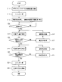
- FIG. 13 is a flowchart of a vapor deposition method using the vapor deposition apparatus according to the first embodiment. The vapor deposition method of this Embodiment 1 is demonstrated using FIG.
- the initial position of the alignment mark is detected at room temperature (step S11). That is, the first identification unit 211 recognizes the first alignment mark 201, and the second identification unit 212 recognizes the second alignment mark 202, and each of the recognized first and second alignment marks 201, 202 is recognized. An absolute position in XY coordinates is detected. If necessary, the rotational drive mechanism 125 is used so that the arrangement direction of the plurality of vapor deposition source openings 61 of the vapor deposition source 60 matches the arrangement direction of the plurality of control plates 81 of the control plate unit 80 (that is, the X-axis direction). The vapor deposition source 60 may be rotated.
- the vapor deposition source 60 may be moved in the X-axis direction using the linear drive mechanism 121 so that the rotation center axis 125a coincides with the center position of the control plate unit 80 in the X-axis direction.
- the vapor deposition source 60 is installed on the rotation drive mechanism 125 so that the rotation center axis
- step S12 the shutter 95 is closed (step S12). Note that the order of step S11 and step S12 may be reversed.
- the vapor deposition source 60 is heated by the heater 63.
- the vapor deposition material is heated and evaporated in the vapor deposition particle generator 65, and the vapor of the vapor deposition material is introduced into the vapor deposition source 60 (step S13).
- release of the vapor deposition particle 91 from the vapor deposition source opening 61 is started.
- the temperature of the vapor deposition source 60, the amount of the vapor deposition particles 91 discharged from the vapor deposition source opening 61, and the like are monitored to determine whether or not vapor deposition is possible (step S14).
- the positional deviation amount of the vapor deposition source 60 with respect to the control plate unit 80 in the X-axis direction is measured (step S15). That is, the first identification unit 211 detects the position of the first alignment mark 201 and compares it with the position detected in step S11, thereby obtaining the displacement amount of the center position of the vapor deposition source 60 in the X-axis direction. Further, the second identification unit 212 detects the position of the second alignment mark 202, and compares it with the position detected in step S11, thereby obtaining the displacement amount of the center position of the control plate unit 80 in the X-axis direction. Then, the amount of positional deviation in the X-axis direction with respect to the control plate unit 80 of the vapor deposition source 60 is obtained from the displacement amount of each central position of the vapor deposition source 60 and the control plate unit 80.
- step S16 it is determined whether or not the amount of positional deviation in the X-axis direction measured in step S15 is equal to or less than a preset threshold value (step S16).
- the threshold value can be set in consideration of the allowable range of the positional deviation amount in the X-axis direction of the vapor deposition source opening 61 with respect to the control plate 81.
- a necessary correction amount is calculated (step S17). That is, the amount of movement of the vapor deposition source 60 in the X-axis direction necessary to reduce the positional deviation amount below the threshold value is calculated.
- step S18 the vapor deposition source 60 is moved in the X-axis direction using the linear drive mechanism 121 according to the correction amount obtained in step S17 (step S18).
- step S15 the process returns to step S15, and the amount of displacement in the X-axis direction with respect to the control plate unit 80 of the vapor deposition source 60 is measured.
- step S16 when the amount of positional deviation measured in step S15 is less than or equal to the threshold value, the difference in thermal expansion amount in the X-axis direction between the vapor deposition source 60 and the control plate unit 80 is measured (step S19). That is, the first identification part 211 detects the position of the first alignment mark 201 and compares it with the position detected in step S11, thereby obtaining the thermal expansion amount of the vapor deposition source 60 in the X-axis direction. Further, the second identification unit 212 detects the position of the second alignment mark 202, and compares it with the position detected in step S11, thereby obtaining the thermal expansion amount of the control plate unit 80 in the X-axis direction. Then, from the respective thermal expansion amounts of the vapor deposition source 60 and the control plate unit 80, a difference in thermal expansion amount in the X-axis direction between the vapor deposition source 60 and the control plate unit 80 is obtained.
- step S20 it is determined whether or not the difference in thermal expansion measured in step S19 is equal to or less than a preset threshold value (step S20).
- the threshold value can be set in consideration of the allowable range of the positional deviation amount in the X-axis direction of the vapor deposition source opening 61 with respect to the control plate 81.
- a necessary correction amount is calculated (step S21). That is, the rotation angle around the rotation center axis 125a of the vapor deposition source 60 necessary to reduce the difference in thermal expansion below the threshold value is calculated.
- step S22 the vapor deposition source 60 is rotated using the rotation drive mechanism 125 according to the correction amount obtained in step S21 (step S22).
- step S19 the process returns to step S19, and the thermal expansion difference in the X-axis direction between the vapor deposition source 60 and the control plate unit 80 is measured.
- step S20 when the difference in thermal expansion measured in step S19 is less than or equal to the threshold value, the shutter 95 is opened (step S23), the substrate 10 is conveyed (step S24), and the deposition surface of the substrate 10 is measured. A film 90 is formed on 10e (see FIG. 12).
- the thermal expansion in the X-axis direction between the vapor deposition source 60 and the control plate unit 80 occurred in the process of raising the temperature from normal temperature to the vapor deposition temperature before the coating 90 is formed. Since the amount difference is detected and corrected, the amount of positional deviation in the X-axis direction of the vapor deposition source opening 61 relative to the control plate 81 due to the difference in thermal expansion amount can be reduced. As a result, a problem of a new deposition method in which the coating film 990 formed on the substrate 10 is displaced in the X-axis direction due to a difference in thermal expansion between the deposition source 960 and the control plate unit 980 (see FIG. 10B). Can be eliminated. That is, according to the first embodiment, the amount of positional deviation in the X-axis direction of the film 90 formed on the substrate 10 can be reduced.
- the positional deviation amount in the X-axis direction of the vapor deposition source 60 with respect to the control plate unit 80 generated in the process of raising the temperature from the normal temperature to the vapor deposition temperature is detected and corrected before the coating 90 is formed,
- the positional shift amount in the X-axis direction of the vapor deposition source opening 61 can be further reduced.
- the amount of positional deviation in the X-axis direction of the film 90 formed on the substrate 10 can be further reduced.
- the vapor deposition source 60 and the control plate unit 80 can be relaxed. Thereby, the production cost of the vapor deposition source 60 and the control plate unit 80 can be reduced, and the production cost of the organic EL display device can be reduced.
- the amount of misalignment in the X-axis direction with respect to the control plate unit 80 of the vapor deposition source 60 can be reduced to an acceptable level in the process of raising the temperature from room temperature to the vapor deposition temperature by devising the design. If possible, steps S15 to S18 shown in FIG. 13 and the linear drive mechanism 121 shown in FIG. 12 may be omitted.
- FIG. 14 is a front cross-sectional view of the vapor deposition apparatus according to Embodiment 2 of the present invention viewed along the scanning direction of the substrate 10.
- the same members as those shown in FIG. 12 are denoted by the same reference numerals, and redundant description thereof will be omitted.
- the second embodiment will be described with a focus on differences from the first embodiment.
- a pair of alignment marks 221 and a pair of recognition units 222 are used instead of the first and second alignment marks 201 and 202 and the first and second recognition units 211 and 212 of the first embodiment.
- Alignment marks 221 are formed on both ends of the control plate unit 80 in the X-axis direction.
- the recognition units 222 are installed at both ends of the vapor deposition source 60 in the X-axis direction. Each recognition unit 222 faces the corresponding alignment mark 221 in the Z-axis direction so that the position of the alignment mark 221 can be recognized.
- the recognition unit 222 is installed on the heat shield plate 69 installed in the vapor deposition source 60 or the heater 63 so that the recognition unit 222 is not heated by the vapor deposition source 60 or the heater 63.
- the heat shield plate 69 can be configured by a cooling plate in which, for example, a water-cooled pipe or the like is incorporated.
- the alignment mark 221 and the recognition unit 222 are arranged at a position that cannot be directly seen from the vapor deposition source opening 61 so that the vapor deposition particles 91 emitted from the vapor deposition source opening 61 are difficult to adhere.
- an adhesion prevention plate (or a shielding plate) for preventing the vapor deposition particles 91 from adhering to the alignment mark 221 and the recognition unit 222 may be installed.
- the configurations of the alignment mark 221 and the recognition unit 222 may be the same as those of the first and second alignment marks 201 and 202 and the first and second recognition units 211 and 212 described in the first embodiment.
- the alignment marks 221 may be formed on both ends of the vapor deposition source 60 in the X-axis direction, and the recognition units 222 may be installed on both ends of the control plate unit 80 in the X-axis direction.
- the heat shield plate 69 may be omitted.
- the vapor deposition using the vapor deposition apparatus according to the second embodiment can be performed in the same manner as FIG. 13 described in the first embodiment. However, steps S11, S15, and S19 are changed as follows.
- the absolute positions of the first and second alignment marks 201 and 202 in the XY coordinates are detected in step S11 of FIG.
- the recognition unit 222 only needs to recognize the alignment mark 221 in step S11.
- step S15 of the second embodiment the alignment mark 221 is recognized by the identification unit 222, and the position thereof is compared with the position of the alignment mark 221 recognized in step S11, so that the X axis with respect to the control plate unit 80 of the vapor deposition source 60 is obtained. Find the amount of misalignment in the direction.
- step S19 of the second embodiment the alignment mark 221 is recognized by the identification unit 222, and the position is compared with the position of the alignment mark 221 identified in step S11. The difference in thermal expansion amount in the X-axis direction is obtained.
- vapor deposition can be performed in the same manner as FIG. 13 described in the first embodiment.
- the first and second alignment marks performed in step S11 of FIG. It is not necessary to measure the absolute position in the XY coordinates. That is, the difference between the thermal expansion amount in the X-axis direction between the vapor deposition source 60 and the control plate unit 80 and the positional deviation amount in the X-axis direction are set to the position of the alignment mark 221 in the image taken by the identification unit 222 at the normal temperature. It can be obtained by comparing with the temperature rise. Therefore, the calculation can be simplified.
- the apparatus cost can be reduced.
- the second embodiment is the same as the first embodiment except for the above, and has the same effect as described in the first embodiment.
- FIG. 15 is a front cross-sectional view of the vapor deposition apparatus according to Embodiment 3 of the present invention, viewed along the scanning direction of the substrate 10.
- the same members as those shown in FIG. 12 are denoted by the same reference numerals, and redundant description thereof will be omitted.
- the third embodiment will be described focusing on differences from the first embodiment.
- a pair of recognition units 232 is used instead of the first and second recognition units 211 and 212 of the first embodiment.
- the pair of recognition units 232 are held by arms that extend from the frame side plate 112 and hold the control plate unit 80.
- a pair of dummy control spaces 82d are formed on both outer sides in the X-axis direction from the region where the plurality of control spaces 82 of the control plate unit 80 are formed.
- the dummy control space 82d is preferably formed at a position where the vapor deposition particles 91 emitted from the vapor deposition source opening 61 hardly enter. Even if the vapor deposition particles 91 are incident on the dummy control space 82 d, the vapor deposition particles 91 do not contribute to the formation of the coating film 90.
- a pair of dummy vapor deposition source openings 61d are formed on both outer sides in the X-axis direction from the region where the plurality of vapor deposition source openings 61 of the vapor deposition source 60 are formed.
- the vapor deposition particles 91 are not emitted from the dummy vapor deposition source opening 61d.
- the recognition unit 232, the dummy control space 82d, and the dummy vapor deposition source opening 61d are arranged substantially along a straight line parallel to the Z axis in this order from the upper side to the lower side.
- the recognition unit 232 recognizes the lower opening edge of the dummy control space 82d and the dummy vapor deposition source opening 61d within one field of view.
- the opening edge of the dummy control space 82d and the dummy vapor deposition source opening 61d function as alignment marks. Therefore, in the third embodiment, the first and second alignment marks 201 and 202 of the first embodiment are not used.
- an adhesion prevention plate (or a shielding plate) for preventing the vapor deposition particles 91 from adhering to the recognition unit 232 may be installed.
- the configuration of the recognition unit 232 may be the same as the first and second recognition units 211 and 212 described in the first embodiment.
- the vapor deposition using the vapor deposition apparatus according to the third embodiment can be performed in the same manner as FIG. 13 described in the first embodiment. However, steps S11, S15, and S19 are changed as follows.
- step S11 the common recognition unit 232 simultaneously detects the absolute position of the opening edge of the dummy control space 82d and the dummy vapor deposition source opening 61d in the XY coordinates.
- step S15 of the third embodiment the positional deviation amount in the X-axis direction with respect to the control plate unit 80 of the vapor deposition source 60 is measured as follows. That is, the position of the dummy vapor deposition source opening 61d is detected by the identification unit 232, and this is compared with the position of the dummy vapor deposition source opening 61d detected in step S11, whereby the displacement amount of the central position in the X-axis direction of the vapor deposition source 60 is detected. Ask for.
- the position of the opening edge of the dummy control space 82d is detected by the identification unit 232, and this is compared with the position of the opening edge of the dummy control space 82d detected in step S11, whereby the X axis of the control plate unit 80 is detected.
- the amount of displacement at the center position in the direction is obtained.
- the amount of positional deviation in the X-axis direction with respect to the control plate unit 80 of the vapor deposition source 60 is obtained from the displacement amount of each central position of the vapor deposition source 60 and the control plate unit 80.
- step S19 of the third embodiment the difference in thermal expansion amount in the X-axis direction between the vapor deposition source 60 and the control plate unit 80 is measured as follows. That is, the position of the dummy vapor deposition source opening 61d is detected by the identification unit 232, and this is compared with the position of the dummy vapor deposition source opening 61d detected in step S11, thereby obtaining the amount of thermal expansion in the X-axis direction of the vapor deposition source 60. .
- the position of the opening edge of the dummy control space 82d is detected by the identification unit 232, and this is compared with the position of the opening edge of the dummy control space 82d detected in step S11, whereby the X axis of the control plate unit 80 is detected. Determine the amount of thermal expansion in the direction. Then, from the respective thermal expansion amounts of the vapor deposition source 60 and the control plate unit 80, a difference in thermal expansion amount in the X-axis direction between the vapor deposition source 60 and the control plate unit 80 is obtained.
- vapor deposition can be performed in the same manner as FIG. 13 described in the first embodiment.
- the common identification unit 232 detects the opening edge of the dummy control space 82d functioning as an alignment mark and the dummy vapor deposition source opening 61d. Therefore, compared to the first embodiment in which the first alignment mark 201 provided on the control plate unit 80 and the second alignment mark 202 provided on the vapor deposition source 60 are recognized by separate identification units, respectively, the vapor deposition source 60 and the control plate unit 80.
- the positional deviation amount in the X-axis direction and the thermal expansion amount difference in the X-axis direction can be obtained more accurately. As a result, the amount of positional deviation in the X-axis direction of the film 90 formed on the substrate 10 can be further reduced.
- the apparatus cost can be reduced.
- the dummy control space 82 and the dummy vapor deposition source opening 61d can be formed by the same method as the control space 82 and the vapor deposition source opening 61, a new process for forming them is unnecessary. Therefore, in the third embodiment, compared with the first embodiment in which the alignment marks 201 and 202 are formed, the device can be easily manufactured and the cost can be reduced.
- the third embodiment is the same as the first embodiment except for the above, and has the same effect as described in the first embodiment.
- FIG. 16 is a flowchart of a vapor deposition method using the vapor deposition apparatus according to Embodiment 4 of the present invention.
- the steps from “START” to step S24 are the same as those in FIG.
- the vapor deposition method of this Embodiment 4 after step S24, ie, after a vapor deposition start, is demonstrated using FIG.
- step S30 it is determined whether or not a predetermined time has elapsed.
- the predetermined time is a time interval for correcting the thermal expansion amount difference and the positional deviation amount, and can be set arbitrarily.
- step S30 When it is confirmed in step S30 that the predetermined time has elapsed, it is determined in step 21 whether or not vapor deposition on the substrate is continued.
- step S31 the amount of positional deviation in the X-axis direction with respect to the control plate unit 80 of the vapor deposition source 60 is measured.
- the measurement of the positional deviation amount can be performed in the same manner as step S15 in FIG.
- step S32 it is determined whether or not the amount of positional deviation in the X-axis direction measured in step S31 is equal to or less than a preset threshold value (step S32).
- the threshold value can be set in consideration of the allowable range of the positional deviation amount in the X-axis direction of the vapor deposition source opening 61 with respect to the control plate 81.
- the value used in step S16 in FIG. 13 can be used.
- step S34 a necessary correction amount is calculated (step S34).
- the calculation of the correction amount can be performed in the same manner as Step S17 in FIG.
- step S35 the vapor deposition source 60 is moved in the X-axis direction using the linear drive mechanism 121 according to the correction amount obtained in step S34 (step S35).
- step S32 the process returns to step S32, and the amount of positional deviation in the X-axis direction with respect to the control plate unit 80 of the vapor deposition source 60 is measured.
- step S33 when the amount of positional deviation measured in step S32 is less than or equal to the threshold value, the difference in thermal expansion amount in the X-axis direction between the vapor deposition source 60 and the control plate unit 80 is measured (step S36).
- the measurement of the difference in thermal expansion can be performed in the same manner as in step S19 in FIG.
- step S37 it is determined whether or not the difference in thermal expansion measured in step S36 is equal to or less than a preset threshold value (step S37).
- the threshold value can be set in consideration of the allowable range of the positional deviation amount in the X-axis direction of the vapor deposition source opening 61 with respect to the control plate 81.
- the value used in step S20 in FIG. 13 can be used.
- step S38 If the thermal expansion amount difference exceeds the threshold value, a necessary correction amount is calculated (step S38). The calculation of the correction amount can be performed in the same manner as Step S21 in FIG.
- step S39 the vapor deposition source 60 is rotated using the rotation drive mechanism 125 according to the correction amount obtained in step S38 (step S39).
- step S36 the process returns to step S36, and the X-axis direction thermal expansion difference between the vapor deposition source 60 and the control plate unit 80 is measured.
- step S37 if the difference in thermal expansion measured in step S36 is less than or equal to the threshold value, the process returns to step S30.
- step S31 when the deposition on the substrate is not continued, the shutter 95 is closed and the deposition process is completed.
- the thermal expansion difference between the vapor deposition source 60 and the control plate unit 80 in the X-axis direction is detected and corrected at predetermined time intervals after the vapor deposition is started.
- the amount of positional deviation in the X-axis direction of the vapor deposition source opening 61 with respect to the control plate 81 due to the amount difference can be reduced.
- a problem of a new deposition method in which the coating film 990 formed on the substrate 10 is displaced in the X-axis direction due to a difference in thermal expansion between the deposition source 960 and the control plate unit 980 see FIG. 10B.
- the amount of positional deviation in the X-axis direction of the coating film 90 formed on the substrate 10 can be further reduced.
- the amount of positional deviation in the X-axis direction of the vapor deposition source 60 with respect to the control plate unit 80 is detected and corrected at predetermined time intervals after the vapor deposition is started, the positional deviation in the X-axis direction of the vapor deposition source opening 61 with respect to the control plate 81 is corrected.
- the amount can be further reduced.
- the amount of positional deviation in the X-axis direction of the film 90 formed on the substrate 10 can be further reduced.
- the fourth embodiment even when the temperatures of the vapor deposition source 60 and the control plate unit 80 change after the vapor deposition starts, the positional deviation in the X-axis direction of the coating film 90 due to such a temperature change is suppressed. be able to.
- step S30 can be omitted.
- the positional deviation amount of the coating film 90 in the X-axis direction can be further reduced.
- step S30 the load required for the arithmetic processing can be reduced.
- the amount of misalignment in the X-axis direction with respect to the control plate unit 80 of the vapor deposition source 60 can be reduced to an acceptable level during the vapor deposition process after the vapor deposition is started by design ingenuity or the like For this, steps S32 to S35 shown in FIG. 16 may be omitted.
- steps S32 and S36 are changed in the same manner as the changes in steps S15 and S19 described in the second and third embodiments.
- the plurality of vapor deposition units 50 shown in FIG. 11 may be arranged with different positions in the X-axis direction and the Y-axis direction.
- the substrate 10 has moved relative to the stationary vapor deposition unit 50.
- the present invention is not limited to this, and one of the vapor deposition unit 50 and the substrate 10 is relative to the other. Move to.
- the position of the substrate 10 may be fixed and the vapor deposition unit 50 may be moved, or both the vapor deposition unit 50 and the substrate 10 may be moved.
- the substrate 10 is disposed above the vapor deposition unit 50, but the relative positional relationship between the vapor deposition unit 50 and the substrate 10 is not limited thereto.
- the substrate 10 may be disposed below the vapor deposition unit 50, or the vapor deposition unit 50 and the substrate 10 may be disposed to face each other in the horizontal direction.
- the application field of the vapor deposition apparatus and vapor deposition method of the present invention is not particularly limited, but can be preferably used for forming a light emitting layer of an organic EL display device.
Landscapes
- Chemical & Material Sciences (AREA)
- Chemical Kinetics & Catalysis (AREA)
- Engineering & Computer Science (AREA)
- Materials Engineering (AREA)
- Mechanical Engineering (AREA)
- Metallurgy (AREA)
- Organic Chemistry (AREA)
- Electroluminescent Light Sources (AREA)
- Physical Vapour Deposition (AREA)
Abstract
Description
本発明を適用して製造可能な有機EL表示装置の一例を説明する。本例の有機EL表示装置は、TFT基板側から光を取り出すボトムエミッション型で、赤(R)、緑(G)、青(B)の各色からなる画素(サブ画素)の発光を制御することによりフルカラーの画像表示を行う有機EL表示装置である。
次に、有機EL表示装置1の製造方法について以下に説明する。
発光層23R,23G,23Bを塗り分け蒸着する方法として、本発明者らは、特許文献1,2のような、蒸着時に基板と同等の大きさのマスクを基板に固定する蒸着方法に代えて、蒸着源及び蒸着マスクに対して基板を移動させながら蒸着を行う新規な蒸着方法(以下、「新蒸着法」という)を検討した。
図5及び図6に示した新蒸着法の上記の問題を解決する塗り分け蒸着方法として、本発明者らは、蒸着源と蒸着マスクとの間に、複数の制御板を配置する蒸着方法(以下、「新々蒸着法」という)を検討した。
図11は、本発明の実施形態1に係る蒸着装置の主要部を示した斜視図である。以下の説明の便宜のため、基板10の幅方向(第1方向)に沿った水平方向軸をX軸、X軸と垂直な水平方向軸をY軸、X軸及びY軸に垂直な上下方向軸をZ軸とするXYZ直交座標系を設定する。Z軸は基板10の被蒸着面の法線方向と平行である。説明の便宜のため、Z軸方向の矢印の側(図11の紙面の上側)を「上側」と称する。
図14は、本発明の実施形態2に係る蒸着装置の、基板10の走査方向に沿って見た正面断面図である。図14において、図12に示した部材と同一の部材には同一の符号が付されており、それらについての重複する説明を省略する。以下、実施形態1と異なる点を中心に、本実施形態2を説明する。
図15は、本発明の実施形態3に係る蒸着装置の、基板10の走査方向に沿って見た正面断面図である。図15において、図12に示した部材と同一の部材には同一の符号が付されており、それらについての重複する説明を省略する。以下、実施形態1と異なる点を中心に、本実施形態3を説明する。
実施形態1では、図13で説明したように、基板への蒸着の開始前に、常温から蒸着時温度まで昇温する過程で生じた、蒸着源60及び制御板ユニット80間のX軸方向の熱膨張量差及びX軸方向の位置ズレ量を補正した。これに対して、本実施形態4では、更に、基板への蒸着を開始した後、蒸着が終了するまでの間に生じる、蒸着源60及び制御板ユニット80間のX軸方向の熱膨張量差及びX軸方向の位置ズレ量を補正する。以下、実施形態1と異なる点を中心に、本実施形態4を説明する。
10e 被蒸着面
20 有機EL素子
23R,23G,23B 発光層
50 蒸着ユニット
60 蒸着源
61 蒸着源開口
70 蒸着マスク
71 マスク開口
80 制御板ユニット
81 制御板
82 制御空間
90 被膜
91 蒸着粒子
95 シャッター
115 直線搬送機構(移動機構)
121 直線駆動機構
125 回転駆動機構
201,202,221 アライメントマーク
211,212,222,232 認識部
Claims (23)
- 基板上に所定パターンの被膜を形成する蒸着方法であって、
前記基板上に蒸着粒子を付着させて前記被膜を形成する蒸着工程を有し、
前記蒸着工程は、前記蒸着粒子を放出する複数の蒸着源開口を備えた蒸着源と、前記複数の蒸着源開口と前記基板との間に配置された蒸着マスクと、前記基板の法線方向に直交する第1方向に沿って配置された複数の制御板を含み、前記蒸着源と前記蒸着マスクとの間に配置された制御板ユニットとを備えた蒸着ユニットを用いて、前記基板と前記蒸着マスクとを一定間隔だけ離間させた状態で、前記基板の法線方向及び前記第1方向に直交する第2方向に沿って前記基板及び前記蒸着ユニットのうちの一方を他方に対して相対的に移動させながら、前記第1方向に隣り合う前記制御板間の空間及び前記蒸着マスクに形成された複数のマスク開口を通過した前記蒸着粒子を前記基板に付着させる工程であり、
前記蒸着源及び前記制御板ユニット間の前記第1方向における熱膨張量差を検出する工程と、
前記熱膨張量差を補正する工程と
を更に有することを特徴とする蒸着方法。 - 前記蒸着源を前記第1方向及び前記第2方向と平行な面内で回転することにより、前記熱膨張量差を補正する請求項1に記載の蒸着方法。
- 前記蒸着源の前記第1方向における中心位置を通る回転中心軸回りに前記蒸着源を回転する請求項2に記載の蒸着方法。
- 前記熱膨張量差を検出する工程と、前記熱膨張量差を補正する工程とを、前記基板上に前記被膜を形成する前に行う請求項1~3のいずれかに記載の蒸着方法。
- 前記熱膨張量差を検出する工程と、前記熱膨張量差を補正する工程とを、前記基板上に前記被膜を形成しながら行う請求項1~4のいずれかに記載の蒸着方法。
- 前記蒸着源及び前記制御板ユニット以外の異なる地点から前記蒸着源及び前記制御板ユニットを別々に観察して、前記熱膨張量差を検出する請求項1~5のいずれかに記載の蒸着方法。
- 前記蒸着源及び前記制御板ユニット以外の共通する地点から前記蒸着源及び前記制御板ユニットを同時に観察して、前記熱膨張量差を検出する請求項1~5のいずれかに記載の蒸着方法。
- 前記蒸着源及び前記制御板ユニットのうちの一方から他方を観察して、前記熱膨張量差を検出する請求項1~5のいずれかに記載の蒸着方法。
- 前記蒸着源及び前記制御板ユニット間の前記第1方向における位置ズレ量を検出する工程と、
前記位置ズレ量を補正する工程と
を更に有する請求項1~8のいずれかに記載の蒸着方法。 - 前記蒸着源を前記第1方向に移動することにより、前記位置ズレ量を補正する請求項9に記載の蒸着方法。
- 前記熱膨張量差を補正する前に、前記位置ズレ量を補正する請求項9又は10に記載の蒸着方法。
- 前記位置ズレ量を検出する工程と、前記位置ズレ量を補正する工程とを、前記基板上に前記被膜を形成する前に行う請求項9~11のいずれかに記載の蒸着方法。
- 前記位置ズレ量を検出する工程と、前記位置ズレ量を補正する工程とを、前記基板上に前記被膜を形成しながら行う請求項9~12のいずれかに記載の蒸着方法。
- 前記蒸着源及び前記制御板ユニット以外の異なる地点から前記蒸着源及び前記制御板ユニットを別々に観察して、前記位置ズレ量を検出する請求項9~13のいずれかに記載の蒸着方法。
- 前記蒸着源及び前記制御板ユニット以外の共通する地点から前記蒸着源及び前記制御板ユニットを同時に観察して、前記位置ズレ量を検出する請求項9~13のいずれかに記載の蒸着方法。
- 前記蒸着源及び前記制御板ユニットのうちの一方から他方を観察して、前記位置ズレ量を検出する請求項9~13のいずれかに記載の蒸着方法。
- 前記被膜が有機EL素子の発光層である請求項1~16のいずれかに記載の蒸着方法。
- 請求項1~16のいずれかに記載の蒸着方法を用いて形成された発光層を備える有機EL表示装置。
- 基板上に所定パターンの被膜を形成する蒸着装置であって、
前記被膜を形成するための蒸着粒子を放出する複数の蒸着源開口を備えた蒸着源、前記複数の蒸着源開口と前記基板との間に配置された蒸着マスク、及び、前記基板の法線方向に直交する第1方向に沿って配置された複数の制御板を含み、前記蒸着源と前記蒸着マスクとの間に配置された制御板ユニットを備えた蒸着ユニットと、
前記基板と前記蒸着マスクとを一定間隔だけ離間させた状態で、前記基板の法線方向及び前記第1方向に直交する第2方向に沿って前記基板及び前記蒸着ユニットのうちの一方を他方に対して相対的に移動させる移動機構と、
前記蒸着源及び前記制御板ユニット間の前記第1方向における熱膨張量差を検出する手段と、
前記熱膨張量差を補正する手段と
を備えることを特徴とする蒸着装置。 - 前記熱膨張量差を補正する手段が、前記蒸着源を前記第1方向及び前記第2方向と平行な面内で回転させる回転駆動機構を含む請求項19に記載の蒸着装置。
- 前記蒸着源及び前記制御板ユニット間の前記第1方向における位置ズレ量を検出する手段と、
前記位置ズレ量を補正する手段と
を更に備える請求項19又は20に記載の蒸着装置。 - 前記位置ズレ量を補正する手段が、前記蒸着源を前記第1方向に移動させる直線駆動機構を含む請求項21に記載の蒸着装置。
- 前記位置ズレ量を検出する手段は、前記熱膨張量差を補正する手段と共通する部材を含む請求項21又は22に記載の蒸着装置。
Priority Applications (3)
| Application Number | Priority Date | Filing Date | Title |
|---|---|---|---|
| CN201180052599.8A CN103189542B (zh) | 2010-10-29 | 2011-10-11 | 蒸镀方法、蒸镀装置和有机el显示装置 |
| JP2012540755A JP5269256B2 (ja) | 2010-10-29 | 2011-10-11 | 蒸着方法及び蒸着装置 |
| US13/824,859 US8609442B2 (en) | 2010-10-29 | 2011-10-11 | Vapor deposition method, vapor deposition device and organic EL display device |
Applications Claiming Priority (2)
| Application Number | Priority Date | Filing Date | Title |
|---|---|---|---|
| JP2010-243646 | 2010-10-29 | ||
| JP2010243646 | 2010-10-29 |
Publications (1)
| Publication Number | Publication Date |
|---|---|
| WO2012056877A1 true WO2012056877A1 (ja) | 2012-05-03 |
Family
ID=45993602
Family Applications (1)
| Application Number | Title | Priority Date | Filing Date |
|---|---|---|---|
| PCT/JP2011/073341 Ceased WO2012056877A1 (ja) | 2010-10-29 | 2011-10-11 | 蒸着方法、蒸着装置、及び有機el表示装置 |
Country Status (4)
| Country | Link |
|---|---|
| US (1) | US8609442B2 (ja) |
| JP (1) | JP5269256B2 (ja) |
| CN (1) | CN103189542B (ja) |
| WO (1) | WO2012056877A1 (ja) |
Cited By (8)
| Publication number | Priority date | Publication date | Assignee | Title |
|---|---|---|---|---|
| JP2014019954A (ja) * | 2012-07-16 | 2014-02-03 | Samsung Display Co Ltd | 有機層蒸着装置、これを用いる有機発光ディスプレイ装置の製造方法、及びこれによって製造された有機発光ディスプレイ装置 |
| KR20140017337A (ko) * | 2012-07-31 | 2014-02-11 | 삼성디스플레이 주식회사 | 증착 장치 및 이를 이용한 증착량 측정 방법 |
| WO2015159428A1 (ja) * | 2014-04-18 | 2015-10-22 | 長州産業株式会社 | ラインソース |
| JP2019145508A (ja) * | 2019-03-27 | 2019-08-29 | 日鉄ケミカル&マテリアル株式会社 | フレキシブル電子デバイスの製造方法 |
| WO2023210096A1 (ja) * | 2022-04-28 | 2023-11-02 | キヤノントッキ株式会社 | 成膜装置、成膜方法、および電子デバイスの製造方法 |
| WO2025079355A1 (ja) * | 2023-10-13 | 2025-04-17 | キヤノントッキ株式会社 | 成膜装置および成膜方法 |
| JP2025066120A (ja) * | 2021-01-25 | 2025-04-22 | 株式会社ジャパンディスプレイ | 表示装置の製造方法 |
| JP7855270B2 (ja) | 2025-01-17 | 2026-05-08 | 株式会社Magnolia White | 表示装置の製造方法 |
Families Citing this family (11)
| Publication number | Priority date | Publication date | Assignee | Title |
|---|---|---|---|---|
| KR101597887B1 (ko) * | 2010-12-20 | 2016-02-25 | 샤프 가부시키가이샤 | 증착 방법 및 증착 장치 |
| CN103238374B (zh) * | 2010-12-27 | 2015-06-24 | 夏普株式会社 | 蒸镀装置、蒸镀方法和有机el显示装置 |
| CN103282538B (zh) * | 2011-01-18 | 2015-04-22 | 夏普株式会社 | 蒸镀装置、蒸镀方法、有机el元件和有机el显示装置 |
| US10312120B2 (en) * | 2013-03-15 | 2019-06-04 | Applied Materials, Inc. | Position and temperature monitoring of ALD platen susceptor |
| JP2015069806A (ja) * | 2013-09-27 | 2015-04-13 | 株式会社ジャパンディスプレイ | 有機エレクトロルミネッセンス表示装置の製造方法 |
| JP6404615B2 (ja) * | 2014-06-26 | 2018-10-10 | シャープ株式会社 | 有機エレクトロルミネッセンス素子製造用マスク、有機エレクトロルミネッセンス素子の製造装置、及び、有機エレクトロルミネッセンス素子の製造方法 |
| DE102015110440A1 (de) * | 2014-11-20 | 2016-05-25 | Aixtron Se | CVD- oder PVD-Reaktor zum Beschichten großflächiger Substrate |
| JP6567349B2 (ja) * | 2015-07-15 | 2019-08-28 | シャープ株式会社 | 蒸着方法及び蒸着装置 |
| CN106591780B (zh) * | 2016-12-22 | 2019-12-31 | 武汉华星光电技术有限公司 | 一种真空蒸镀机及其蒸镀方法 |
| KR102516885B1 (ko) * | 2018-05-10 | 2023-03-30 | 삼성전자주식회사 | 증착 장비 및 이를 이용한 반도체 장치 제조 방법 |
| CN110212013B (zh) | 2019-07-19 | 2022-01-28 | 京东方科技集团股份有限公司 | Oled背板结构和oled背板结构的制作方法 |
Citations (3)
| Publication number | Priority date | Publication date | Assignee | Title |
|---|---|---|---|---|
| JP2003157973A (ja) * | 2001-09-05 | 2003-05-30 | Sony Corp | 有機電界発光素子の製造方法および製造装置並びに有機電界発光素子を用いた表示装置の製造システムおよび製造方法 |
| JP2008208443A (ja) * | 2007-02-28 | 2008-09-11 | Sony Corp | 蒸着成膜装置、蒸着成膜方法、および表示装置の製造方法 |
| JP2010242116A (ja) * | 2009-04-01 | 2010-10-28 | Fujifilm Corp | 成膜方法と成膜装置、マスク、パターン膜、光電変換素子、及び太陽電池 |
Family Cites Families (5)
| Publication number | Priority date | Publication date | Assignee | Title |
|---|---|---|---|---|
| JP3401356B2 (ja) | 1995-02-21 | 2003-04-28 | パイオニア株式会社 | 有機エレクトロルミネッセンスディスプレイパネルとその製造方法 |
| JP3019095B1 (ja) | 1998-12-22 | 2000-03-13 | 日本電気株式会社 | 有機薄膜elデバイスの製造方法 |
| US20030232563A1 (en) | 2002-05-09 | 2003-12-18 | Isao Kamiyama | Method and apparatus for manufacturing organic electroluminescence device, and system and method for manufacturing display unit using organic electroluminescence devices |
| TWI252706B (en) * | 2002-09-05 | 2006-04-01 | Sanyo Electric Co | Manufacturing method of organic electroluminescent display device |
| JP5064810B2 (ja) | 2006-01-27 | 2012-10-31 | キヤノン株式会社 | 蒸着装置および蒸着方法 |
-
2011
- 2011-10-11 WO PCT/JP2011/073341 patent/WO2012056877A1/ja not_active Ceased
- 2011-10-11 CN CN201180052599.8A patent/CN103189542B/zh active Active
- 2011-10-11 JP JP2012540755A patent/JP5269256B2/ja active Active
- 2011-10-11 US US13/824,859 patent/US8609442B2/en not_active Expired - Fee Related
Patent Citations (3)
| Publication number | Priority date | Publication date | Assignee | Title |
|---|---|---|---|---|
| JP2003157973A (ja) * | 2001-09-05 | 2003-05-30 | Sony Corp | 有機電界発光素子の製造方法および製造装置並びに有機電界発光素子を用いた表示装置の製造システムおよび製造方法 |
| JP2008208443A (ja) * | 2007-02-28 | 2008-09-11 | Sony Corp | 蒸着成膜装置、蒸着成膜方法、および表示装置の製造方法 |
| JP2010242116A (ja) * | 2009-04-01 | 2010-10-28 | Fujifilm Corp | 成膜方法と成膜装置、マスク、パターン膜、光電変換素子、及び太陽電池 |
Cited By (14)
| Publication number | Priority date | Publication date | Assignee | Title |
|---|---|---|---|---|
| JP2014019954A (ja) * | 2012-07-16 | 2014-02-03 | Samsung Display Co Ltd | 有機層蒸着装置、これを用いる有機発光ディスプレイ装置の製造方法、及びこれによって製造された有機発光ディスプレイ装置 |
| US10596582B2 (en) | 2012-07-31 | 2020-03-24 | Samsung Display Co., Ltd. | Depositing apparatus and method for measuring deposition quantity using the same |
| KR20140017337A (ko) * | 2012-07-31 | 2014-02-11 | 삼성디스플레이 주식회사 | 증착 장치 및 이를 이용한 증착량 측정 방법 |
| JP2014031581A (ja) * | 2012-07-31 | 2014-02-20 | Samsung Display Co Ltd | 蒸着装置およびこれを用いた蒸着量測定方法 |
| US9724715B2 (en) | 2012-07-31 | 2017-08-08 | Samsung Display Co., Ltd | Depositing apparatus and method for measuring deposition quantity using the same |
| KR101938365B1 (ko) * | 2012-07-31 | 2019-04-12 | 삼성디스플레이 주식회사 | 증착 장치 및 이를 이용한 증착량 측정 방법 |
| WO2015159428A1 (ja) * | 2014-04-18 | 2015-10-22 | 長州産業株式会社 | ラインソース |
| JP2019145508A (ja) * | 2019-03-27 | 2019-08-29 | 日鉄ケミカル&マテリアル株式会社 | フレキシブル電子デバイスの製造方法 |
| JP2025066120A (ja) * | 2021-01-25 | 2025-04-22 | 株式会社ジャパンディスプレイ | 表示装置の製造方法 |
| WO2023210096A1 (ja) * | 2022-04-28 | 2023-11-02 | キヤノントッキ株式会社 | 成膜装置、成膜方法、および電子デバイスの製造方法 |
| JP2023163217A (ja) * | 2022-04-28 | 2023-11-10 | キヤノントッキ株式会社 | 成膜装置、成膜方法、および電子デバイスの製造方法 |
| JP7812280B2 (ja) | 2022-04-28 | 2026-02-09 | キヤノントッキ株式会社 | 成膜装置、成膜方法、および電子デバイスの製造方法 |
| WO2025079355A1 (ja) * | 2023-10-13 | 2025-04-17 | キヤノントッキ株式会社 | 成膜装置および成膜方法 |
| JP7855270B2 (ja) | 2025-01-17 | 2026-05-08 | 株式会社Magnolia White | 表示装置の製造方法 |
Also Published As
| Publication number | Publication date |
|---|---|
| CN103189542B (zh) | 2014-12-03 |
| US8609442B2 (en) | 2013-12-17 |
| JP5269256B2 (ja) | 2013-08-21 |
| CN103189542A (zh) | 2013-07-03 |
| US20130196454A1 (en) | 2013-08-01 |
| JPWO2012056877A1 (ja) | 2014-03-20 |
Similar Documents
| Publication | Publication Date | Title |
|---|---|---|
| JP5269256B2 (ja) | 蒸着方法及び蒸着装置 | |
| JP5259886B2 (ja) | 蒸着方法及び蒸着装置 | |
| JP5623598B2 (ja) | 蒸着装置、蒸着方法、並びに、有機エレクトロルミネッセンス表示装置の製造方法 | |
| JP5350547B2 (ja) | 被成膜基板および有機el表示装置 | |
| JP5612106B2 (ja) | 蒸着方法、蒸着装置、及び有機el表示装置 | |
| JP5766239B2 (ja) | 蒸着装置及び蒸着方法 | |
| JP5384755B2 (ja) | 被成膜基板、有機el表示装置 | |
| JP6567349B2 (ja) | 蒸着方法及び蒸着装置 | |
| JP6199967B2 (ja) | 有機エレクトロルミネッセンス素子の製造方法 | |
| JP6429491B2 (ja) | 蒸着装置用マスク、蒸着装置、蒸着方法、及び、有機エレクトロルミネッセンス素子の製造方法 | |
| WO2012099019A1 (ja) | 被成膜基板、有機el表示装置および蒸着方法 | |
| WO2015186796A1 (ja) | 蒸着方法及び蒸着装置 | |
| WO2012090777A1 (ja) | 蒸着方法、蒸着膜および有機エレクトロルミネッセンス表示装置の製造方法 | |
| JP5313406B2 (ja) | 被成膜基板、有機el表示装置 | |
| US9614155B2 (en) | Vapor deposition apparatus, vapor deposition method, and method for producing organic electroluminescent element | |
| WO2012108363A1 (ja) | 坩堝、蒸着装置、蒸着方法、有機エレクトロルミネッセンス表示装置の製造方法 |
Legal Events
| Date | Code | Title | Description |
|---|---|---|---|
| 121 | Ep: the epo has been informed by wipo that ep was designated in this application |
Ref document number: 11836016 Country of ref document: EP Kind code of ref document: A1 |
|
| ENP | Entry into the national phase |
Ref document number: 2012540755 Country of ref document: JP Kind code of ref document: A |
|
| WWE | Wipo information: entry into national phase |
Ref document number: 13824859 Country of ref document: US |
|
| NENP | Non-entry into the national phase |
Ref country code: DE |
|
| 122 | Ep: pct application non-entry in european phase |
Ref document number: 11836016 Country of ref document: EP Kind code of ref document: A1 |