WO2012108363A1 - 坩堝、蒸着装置、蒸着方法、有機エレクトロルミネッセンス表示装置の製造方法 - Google Patents
坩堝、蒸着装置、蒸着方法、有機エレクトロルミネッセンス表示装置の製造方法 Download PDFInfo
- Publication number
- WO2012108363A1 WO2012108363A1 PCT/JP2012/052549 JP2012052549W WO2012108363A1 WO 2012108363 A1 WO2012108363 A1 WO 2012108363A1 JP 2012052549 W JP2012052549 W JP 2012052549W WO 2012108363 A1 WO2012108363 A1 WO 2012108363A1
- Authority
- WO
- WIPO (PCT)
- Prior art keywords
- vapor deposition
- injection
- film formation
- particles
- substrate
- Prior art date
Links
Images


Classifications
-
- C—CHEMISTRY; METALLURGY
- C23—COATING METALLIC MATERIAL; COATING MATERIAL WITH METALLIC MATERIAL; CHEMICAL SURFACE TREATMENT; DIFFUSION TREATMENT OF METALLIC MATERIAL; COATING BY VACUUM EVAPORATION, BY SPUTTERING, BY ION IMPLANTATION OR BY CHEMICAL VAPOUR DEPOSITION, IN GENERAL; INHIBITING CORROSION OF METALLIC MATERIAL OR INCRUSTATION IN GENERAL
- C23C—COATING METALLIC MATERIAL; COATING MATERIAL WITH METALLIC MATERIAL; SURFACE TREATMENT OF METALLIC MATERIAL BY DIFFUSION INTO THE SURFACE, BY CHEMICAL CONVERSION OR SUBSTITUTION; COATING BY VACUUM EVAPORATION, BY SPUTTERING, BY ION IMPLANTATION OR BY CHEMICAL VAPOUR DEPOSITION, IN GENERAL
- C23C14/00—Coating by vacuum evaporation, by sputtering or by ion implantation of the coating forming material
- C23C14/06—Coating by vacuum evaporation, by sputtering or by ion implantation of the coating forming material characterised by the coating material
- C23C14/12—Organic material
-
- C—CHEMISTRY; METALLURGY
- C23—COATING METALLIC MATERIAL; COATING MATERIAL WITH METALLIC MATERIAL; CHEMICAL SURFACE TREATMENT; DIFFUSION TREATMENT OF METALLIC MATERIAL; COATING BY VACUUM EVAPORATION, BY SPUTTERING, BY ION IMPLANTATION OR BY CHEMICAL VAPOUR DEPOSITION, IN GENERAL; INHIBITING CORROSION OF METALLIC MATERIAL OR INCRUSTATION IN GENERAL
- C23C—COATING METALLIC MATERIAL; COATING MATERIAL WITH METALLIC MATERIAL; SURFACE TREATMENT OF METALLIC MATERIAL BY DIFFUSION INTO THE SURFACE, BY CHEMICAL CONVERSION OR SUBSTITUTION; COATING BY VACUUM EVAPORATION, BY SPUTTERING, BY ION IMPLANTATION OR BY CHEMICAL VAPOUR DEPOSITION, IN GENERAL
- C23C14/00—Coating by vacuum evaporation, by sputtering or by ion implantation of the coating forming material
- C23C14/22—Coating by vacuum evaporation, by sputtering or by ion implantation of the coating forming material characterised by the process of coating
- C23C14/24—Vacuum evaporation
-
- H—ELECTRICITY
- H10—SEMICONDUCTOR DEVICES; ELECTRIC SOLID-STATE DEVICES NOT OTHERWISE PROVIDED FOR
- H10K—ORGANIC ELECTRIC SOLID-STATE DEVICES
- H10K71/00—Manufacture or treatment specially adapted for the organic devices covered by this subclass
- H10K71/10—Deposition of organic active material
- H10K71/16—Deposition of organic active material using physical vapour deposition [PVD], e.g. vacuum deposition or sputtering
- H10K71/164—Deposition of organic active material using physical vapour deposition [PVD], e.g. vacuum deposition or sputtering using vacuum deposition
Definitions
- the present invention relates to a vapor deposition technique for forming a pattern of vapor deposition particles on a film formation substrate.
- flat panel displays have been used in various products and fields, and further flat panel displays are required to have larger sizes, higher image quality, and lower power consumption.
- an organic EL display device including an organic EL element using electroluminescence (hereinafter referred to as “EL”) of an organic material is an all-solid-state type, low voltage driving, high speed response, As a flat panel display excellent in terms of self-luminous property and the like, it is attracting a great deal of attention.
- the organic EL display device has, for example, a configuration in which an organic EL element connected to a TFT is provided on a substrate made of a glass substrate or the like provided with a TFT (thin film transistor).
- the organic EL element is a light emitting element that can emit light with high luminance by low-voltage direct current drive, and has a structure in which a first electrode, an organic EL layer, and a second electrode are stacked in this order. Of these, the first electrode is connected to the TFT. In addition, between the first electrode and the second electrode, as the organic EL layer, a hole injection layer, a hole transport layer, an electron blocking layer, a light emitting layer, a hole blocking layer, an electron transport layer, an electron injection layer The organic layer which laminated
- organic EL elements including light emitting layers of red (R), green (G), and blue (B) are arranged and formed on a substrate as sub-pixels. A color image is displayed by selectively emitting light from these organic EL elements with a desired luminance using TFTs.
- an organic EL display device In order to manufacture an organic EL display device, it is necessary to form a light emitting layer made of an organic light emitting material that emits light of each color in a predetermined pattern for each organic EL element. In addition, for a layer that does not require pattern formation for each organic EL element, a thin film is collectively formed on the entire pixel region constituted by the organic EL element.
- a vacuum deposition method for example, a vacuum deposition method, an ink jet method, and a laser transfer method are known.
- a vacuum deposition method is often used.
- a mask also referred to as a deposition mask in which openings having a predetermined pattern are formed is used.
- the deposition surface of the substrate to which the mask is closely fixed is opposed to the deposition source.
- vapor deposition particles film forming material from the vapor deposition source are vapor deposited on the vapor deposition surface through the opening of the mask, thereby forming a thin film having a predetermined pattern.
- Vapor deposition is performed for each color of the light emitting layer (this is called “separate vapor deposition”).
- the evaporation source 201 of the evaporation material and the evaporation material Va which is installed on the opposite side of the evaporation source 201 from the evaporation region R where the evaporation material Va is to be deposited are reflected.
- the vapor deposition apparatus 200 provided with the reflecting member 202 to perform is disclosed.
- the reflecting member 202 of Patent Document 1 is configured such that the cross section has a concave curve and extends in a direction perpendicular to the cross section, and the evaporation source 201 is disposed near the focal point of the curve. ing.
- Japanese Patent Publication Japanese Patent Laid-Open No. 2008-138261 (published on June 19, 2008)
- the entire member constituting the evaporation source 201 (hereinafter referred to as a vapor deposition source component member) is installed in the flow area of the reflected evaporation substance. For this reason, the vapor deposition flow is disturbed by the vapor deposition source component member, and the film thickness distribution of the vapor deposition film on the target surface on which the vapor deposition film is formed is not uniform, or the rate at which the vapor deposition material is deposited on the vapor deposition film formation target surface is reduced. It can be considered that this problem occurs.
- the present invention has been made in view of the above-described problems, and provides a crucible, a vapor deposition apparatus, a vapor deposition method, and a method for manufacturing an organic electroluminescence display device that can prevent a decrease in the vapor deposition rate as much as possible. With the goal.
- a crucible according to the present invention comprises a vapor deposition particle injection member provided with an injection port for injecting vapor deposition particles for forming a vapor deposition film on a deposition film formation target surface of a deposition target substrate, A reflective surface having a concave curved shape that reflects the vapor deposition particles emitted from the injection port toward the vapor deposition film formation target surface, and at least a part of the vapor deposition particle injection member forms the reflection surface and the vapor deposition film. It is installed so that it may be located in the exterior of the flow area of the vapor deposition particle between target surfaces.
- the vapor deposition method according to the present invention is a vapor deposition method for forming a vapor deposition film on a vapor deposition film formation target surface of a deposition target substrate, and an injection step of injecting vapor deposition particles from an injection port of a vapor deposition particle injection member;
- the vapor deposition particle injection member is installed so that at least a part thereof is located outside the flow area of the vapor deposition particles between the reflective surface and the vapor deposition film formation target surface. It is possible to prevent as much as possible a situation in which the flow of vapor deposition particles (hereinafter referred to as vapor deposition flow) is disturbed by the injection member and the film thickness of the vapor deposition film on the vapor deposition film formation target surface is not uniform.
- the organic electroluminescence display device manufacturing method includes a TFT substrate / first electrode manufacturing step of forming a first electrode on a TFT substrate, and an organic layer including an organic layer including at least a light-emitting layer on the TFT substrate.
- An organic electroluminescence display device comprising: a layer vapor deposition step; a second electrode vapor deposition step of vapor depositing a second electrode; and a sealing step of sealing an organic electroluminescence element including the organic layer and the second electrode with a sealing member
- the method of manufacturing, wherein at least one of the organic layer deposition step, the second electrode deposition step, and the sealing step includes each step of any one of the deposition methods. It is.
- the film thickness distribution is made uniform while obtaining a constant deposition rate, an organic electroluminescence display device with little display unevenness can be realized.
- the crucible according to the present invention includes a vapor deposition particle injection member provided with an injection port for injecting vapor deposition particles for forming a vapor deposition film on a surface on which a vapor deposition film is to be formed, and vapor deposition particles injected from the injection port And a concavely curved reflecting surface that reflects toward the surface on which the vapor deposition film is to be formed, and at least part of the vapor deposition particle injection member is vapor deposition particles between the reflection surface and the surface on which the vapor deposition film is to be formed. It is installed outside the basin.
- the vapor deposition method according to the present invention is a vapor deposition method for forming a vapor deposition film on a vapor deposition film formation target surface of a deposition target substrate, and an injection step of injecting vapor deposition particles from an injection port of a vapor deposition particle injection member;
- the vapor deposition particle injection member is disposed so that at least a part thereof is located outside the flow area of the vapor deposition particles between the reflection surface and the vapor deposition film formation target surface, and thus vapor deposition is performed by the vapor deposition particle injection member. It is possible to prevent or suppress as much as possible the situation that the flow is disturbed and the film thickness of the vapor deposition film on the vapor deposition film formation target surface is not uniform.
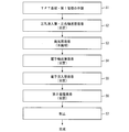
- FIG. 1 It is a schematic diagram of the vapor deposition apparatus which concerns on the 1st Embodiment of this invention. It is a figure which shows the specific structure of a vapor deposition apparatus. It is a figure which shows the structure of a crucible. It is a disassembled perspective view which shows the structure of the container for injection. It is a figure for demonstrating a parabola principle. It is a figure for demonstrating the function of a reflective surface. It is the figure which showed the result of having formed the vapor deposition film on the film-forming board
- FIG. 10 is a cross-sectional view taken along line AA of the TFT substrate in the organic EL display device shown in FIG. 9.
- It is a flowchart which shows the manufacturing process of the organic electroluminescence display concerning the 1st Embodiment of this invention in process order.
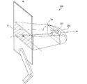
- It is a model perspective view which shows the external appearance structure of the crucible which concerns on the 2nd Embodiment of this invention.
- FIG. 1 It is a figure which shows the vapor deposition apparatus which concerns on the 3rd Embodiment of this invention. It is a perspective view which shows arrangement
- a method for manufacturing a bottom emission type organic EL display device for RGB full color display in which light is extracted from the TFT substrate side is given as an example. explain.
- FIG. 8 is a cross-sectional view showing a schematic configuration of an organic EL display device for RGB full color display.
- 9 is a plan view showing a configuration of a pixel constituting the organic EL display device shown in FIG. 8, and
- FIG. 10 is a cross-sectional view taken along line AA of the TFT substrate in the organic EL display device shown in FIG. FIG.
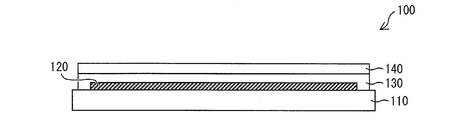
- the organic EL display device 100 manufactured in this embodiment includes an organic EL element 120 connected to a TFT 112, an adhesive layer on a TFT substrate 110 provided with a TFT 112 (see FIG. 10). 130 and the sealing substrate 140 have the structure provided in this order.
- the organic EL element 120 includes a pair of substrates (TFT substrates) by bonding a TFT substrate 110 on which the organic EL element 120 is laminated to a sealing substrate 140 using an adhesive layer 130. 110, sealing substrate 140).
- TFT substrates substrates
- the organic EL element 120 is sealed between the TFT substrate 110 and the sealing substrate 140 as described above, so that oxygen or moisture can enter the organic EL element 120 from the outside. It is prevented.
- the TFT substrate 110 includes a transparent insulating substrate 111 such as a glass substrate as a supporting substrate.
- a plurality of wirings 114 each including a plurality of gate lines laid in the horizontal direction and a plurality of signal lines laid in the vertical direction and intersecting the gate lines are provided. It has been.
- a gate line driving circuit (not shown) for driving the gate line is connected to the gate line, and a signal line driving circuit (not shown) for driving the signal line is connected to the signal line.
- the organic EL display device 100 is a full-color active matrix type organic EL display device. On the insulating substrate 111, red (R), green (G), and blue are shown in regions surrounded by the wirings 114, respectively.
- the sub-pixels 102R, 102G, and 102B of the respective colors including the organic EL elements 120 of the respective colors (B) are arranged in a matrix.
- a region surrounded by these wirings 114 is one subpixel (dot), and R, G, and B light emitting regions are defined for each subpixel.
- the pixel (that is, one pixel) has three sub-pixels: a red sub-pixel 102R that transmits red light, a green sub-pixel 102G that transmits green light, and a blue sub-pixel 102B that transmits blue light. 102R / 102G / 102B.
- Each of the sub-pixels 102R, 102G, and 102B includes openings 115R and 115G that are covered with stripe-shaped light-emitting layers 123R, 123G, and 123B as light-emitting regions of the respective colors that emit light in the sub-pixels 102R, 102G, and 102B. -115B is provided.
- the light emitting layers 123R, 123G, and 123B are patterned by vapor deposition for each color.
- the openings 115R, 115G, and 115B will be described later.
- These sub-pixels 102R, 102G, and 102B are provided with TFTs 112 connected to the first electrode 121 in the organic EL element 120, respectively.
- the light emission intensity of each of the sub-pixels 102R, 102G, and 102B is determined by scanning and selection by the wiring 114 and the TFT 112.
- the organic EL display device 100 realizes image display by selectively causing the organic EL element 120 to emit light with a desired luminance using the TFT 112.
- the TFT substrate 110 will be described.
- the TFT substrate 110 has a TFT 112 (switching element), an interlayer film 113 (interlayer insulating film, planarization film), a wiring 114, and an edge cover 115 on a transparent insulating substrate 111 such as a glass substrate. It has the structure formed in this order.
- TFTs 112 are provided corresponding to the sub-pixels 102R, 102G, and 102B, respectively.
- the structure of the TFT is conventionally well known. Therefore, illustration and description of each layer in the TFT 112 are omitted.
- the interlayer film 113 is laminated on the insulating substrate 111 over the entire area of the insulating substrate 111 so as to cover the TFTs 112.
- the first electrode 121 in the organic EL element 120 is formed.
- the interlayer film 113 is provided with a contact hole 113a for electrically connecting the first electrode 121 in the organic EL element 120 to the TFT 112. Thereby, the TFT 112 is electrically connected to the organic EL element 120 through the contact hole 113a.
- the edge cover 115 detects that the first electrode 121 and the second electrode 126 in the organic EL element 120 are short-circuited when the organic EL layer becomes thin or the electric field concentration occurs at the pattern end of the first electrode 121. It is an insulating layer for preventing.
- the edge cover 115 is formed on the interlayer film 113 so as to cover the pattern end of the first electrode 121.
- the edge cover 115 is provided with openings 115R, 115G, and 115B for each of the sub-pixels 102R, 102G, and 102B.
- the openings 115R, 115G, and 115B of the edge cover 115 serve as light emitting regions of the sub-pixels 102R, 102G, and 102B.
- the sub-pixels 102R, 102G, and 102B are partitioned by the edge cover 115 having an insulating property.
- the edge cover 115 also functions as an element isolation film.
- the organic EL element 120 is a light emitting element that can emit light with high luminance by low-voltage direct current drive, and a first electrode 121, an organic EL layer, and a second electrode 126 are stacked in this order.
- the first electrode 121 is a layer having a function of injecting (supplying) holes into the organic EL layer. As described above, the first electrode 121 is connected to the TFT 112 through the contact hole 113a.
- a hole injection layer / hole transport layer 122, light emitting layers 123R, 123G, 123B, the electron carrying layer 124, and the electron injection layer 125 have the structure formed in this order.
- the stacking order is that in which the first electrode 121 is an anode and the second electrode 126 is a cathode, and when the first electrode 121 is a cathode and the second electrode 126 is an anode, the organic EL layer is used. The order of stacking is reversed.
- the hole injection layer is a layer having a function of increasing the hole injection efficiency into the light emitting layers 123R, 123G, and 123B.
- the hole transport layer is a layer having a function of improving the efficiency of transporting holes to the light emitting layers 123R, 123G, and 123B.
- the hole injection / hole transport layer 122 is uniformly formed on the entire display region of the TFT substrate 110 so as to cover the first electrode 121 and the edge cover 115.
- the hole injection layer / hole transport layer 122 in which the hole injection layer and the hole transport layer are integrated is provided as the hole injection layer and the hole transport layer.
- An example will be described.
- the present embodiment is not limited to this.
- the hole injection layer and the hole transport layer may be formed as independent layers.
- the light emitting layers 123R, 123G, and 123B correspond to the sub-pixels 102R, 102G, and 102B so as to cover the openings 115R, 115G, and 115B of the edge cover 115, respectively. Is formed.
- the light emitting layers 123R, 123G, and 123B are layers having a function of emitting light by recombining holes injected from the first electrode 121 side with electrons injected from the second electrode 126 side. .
- the light emitting layers 123R, 123G, and 123B are each formed of a material having high light emission efficiency, such as a low molecular fluorescent dye or a metal complex.
- the electron transport layer 124 is a layer having a function of increasing the electron transport efficiency from the second electrode 126 to the light emitting layers 123R, 123G, and 123B.
- the electron injection layer 125 is a layer having a function of increasing the electron injection efficiency from the second electrode 126 to the light emitting layers 123R, 123G, and 123B.
- the electron transport layer 124 is formed on the light emitting layer 123R / 123G / 123B and the hole injection layer / hole transport layer 122 so as to cover the light emitting layer 123R / 123G / 123B and the hole injection layer / hole transport layer 122.
- the TFT substrate 110 is uniformly formed over the entire display area.
- the electron injection layer 125 is uniformly formed on the entire surface of the display region of the TFT substrate 110 on the electron transport layer 124 so as to cover the electron transport layer 124.
- the electron transport layer 124 and the electron injection layer 125 may be formed as independent layers as described above, or may be provided integrally with each other. That is, the organic EL display device 100 may include an electron transport layer / electron injection layer instead of the electron transport layer 124 and the electron injection layer 125.
- the second electrode 126 is a layer having a function of injecting electrons into the organic EL layer composed of the organic layers as described above.
- the second electrode 126 is uniformly formed on the electron injection layer 125 over the entire display region of the TFT substrate 110 so as to cover the electron injection layer 125.
- organic layers other than the light-emitting layers 123R, 123G, and 123B are not essential layers as the organic EL layer, and may be appropriately formed according to the required characteristics of the organic EL element 120.
- a carrier blocking layer can also be added to the organic EL layer as necessary. For example, by adding a hole blocking layer as a carrier blocking layer between the light emitting layers 123R, 123G, and 123B and the electron transport layer 124, holes are prevented from passing through the electron transport layer 124, thereby improving luminous efficiency. can do.
- first electrode / light emitting layer / second electrode (2) First electrode / hole transport layer / light emitting layer / electron transport layer / second electrode (3) First electrode / hole transport layer / light emitting layer / Hole blocking layer (carrier blocking layer) / electron transport layer / second electrode (4) first electrode / hole transport layer / light emitting layer / hole blocking layer / electron transport layer / electron injection layer / second electrode (5 ) 1st electrode / hole injection layer / hole transport layer / light emitting layer / electron transport layer / electron injection layer / second electrode (6) 1st electrode / hole injection layer / hole transport layer / light emitting layer / positive Hole blocking layer / electron transport layer / second electrode (7) first electrode / hole injection layer / hole transport layer / light emitting layer / hole blocking layer / electron transport layer / electron injection layer / second electrode (8) 1st electrode
- the configuration of the organic EL element 120 is not limited to the above-described exemplary layer configuration, and a desired layer configuration can be adopted according to the required characteristics of the organic EL element 120 as described above.
- FIG. 11 is a flowchart showing the manufacturing process of the organic EL display device 100 in the order of steps.
- the manufacturing method of the organic EL display device 100 includes, for example, a TFT substrate / first electrode manufacturing step (S1), a hole injection layer / hole transport layer deposition configuration (S2). ), A light emitting layer vapor deposition step (S3), an electron transport layer vapor deposition step (S4), an electron injection layer vapor deposition step (S5), a second electrode vapor deposition step (S6), and a sealing step (S7).
- the stacking order described in the present embodiment uses the first electrode 121 as an anode and the second electrode 126 as a cathode, and conversely, uses the first electrode 121 as a cathode and the second electrode 126. Is used as the anode, the stacking order of the organic EL layers is reversed. Similarly, the materials constituting the first electrode 121 and the second electrode 126 are also inverted.
- a photosensitive resin is applied on an insulating substrate 111 such as glass on which TFTs 112 and wirings 114 are formed by a known technique, and patterning is performed by a photolithography technique, thereby insulating substrate 111.
- An interlayer film 113 is formed thereon.
- the insulating substrate 111 has, for example, a thickness of 0.7 to 1.1 mm, a length in the y-axis direction (vertical length) of 400 to 500 mm, and a length in the x-axis direction (horizontal length) of 300.
- a glass substrate or a plastic substrate of ⁇ 400 mm is used. In this embodiment, a glass substrate is used.
- an acrylic resin or a polyimide resin can be used as the interlayer film 113.
- the acrylic resin include Optomer series manufactured by JSR Corporation.
- a polyimide resin the photo nice series by Toray Industries, Inc. is mentioned, for example.
- the polyimide resin is generally not transparent but colored. Therefore, when a bottom emission type organic EL display device is manufactured as the organic EL display device 100 as shown in FIG. 10, a transparent resin such as an acrylic resin is more preferably used as the interlayer film 113. Used.
- the film thickness of the interlayer film 113 is not particularly limited as long as the step due to the TFT 112 can be compensated. In this embodiment, for example, the thickness is about 2 ⁇ m.
- a contact hole 113 a for electrically connecting the first electrode 121 to the TFT 112 is formed in the interlayer film 113.
- an ITO (Indium Tin Oxide: Indium Tin Oxide) film is formed with a thickness of 100 nm by a sputtering method or the like.
- the ITO film is etched using ferric chloride as an etchant. Thereafter, the photoresist is stripped using a resist stripping solution, and substrate cleaning is further performed. As a result, the first electrodes 121 are formed in a matrix on the interlayer film 113.
- Examples of the conductive film material used for the first electrode 121 include transparent conductive materials such as ITO, IZO (Indium Zinc Oxide), gallium-doped zinc oxide (GZO), gold (Au), Metal materials such as nickel (Ni) and platinum (Pt) can be used.
- transparent conductive materials such as ITO, IZO (Indium Zinc Oxide), gallium-doped zinc oxide (GZO), gold (Au), Metal materials such as nickel (Ni) and platinum (Pt) can be used.
- a method for laminating the conductive film in addition to the sputtering method, a vacuum deposition method, a CVD (chemical vapor deposition) method, a plasma CVD method, a printing method, or the like can be used.
- the thickness of the first electrode 121 is not particularly limited, it can be set to, for example, a thickness of 100 nm as described above.
- the edge cover 115 is patterned and formed with a film thickness of about 1 ⁇ m, for example.
- an insulating material similar to that of the interlayer film 113 can be used.
- the TFT substrate 110 and the first electrode 121 are manufactured (S1).
- the TFT substrate 110 that has undergone the above-described steps is subjected to oxygen plasma treatment as a vacuum baking for dehydration and surface cleaning of the first electrode 121.
- a hole injection layer and a hole transport layer are displayed on the TFT substrate 110 on the TFT substrate 110 using a conventional deposition apparatus. Vapor deposition is performed on the entire area (S2).
- an open mask having an entire display area opened is aligned and adhered to the TFT substrate 110 and then scattered from the evaporation source while rotating the TFT substrate 110 and the open mask together. Vapor deposition particles are uniformly deposited on the entire display region through the opening of the open mask.
- vapor deposition on the entire surface of the display area means that vapor deposition is performed continuously between adjacent sub-pixels of different colors.
- Examples of the material for the hole injection layer and the hole transport layer include benzine, styrylamine, triphenylamine, porphyrin, triazole, imidazole, oxadiazole, polyarylalkane, phenylenediamine, arylamine, oxazole, anthracene, and fluorenone. , Hydrazone, stilbene, triphenylene, azatriphenylene, and derivatives thereof, polysilane compounds, vinylcarbazole compounds, thiophene compounds, aniline compounds, etc., heterocyclic or chain conjugated monomers, oligomers, or polymers , Etc.
- the hole injection layer and the hole transport layer may be integrated as described above, or may be formed as independent layers.
- Each film thickness is, for example, 10 to 100 nm.
- the hole injection layer / hole transport layer 122 is provided as the hole injection layer and the hole transport layer, and 4,4′-bis [ N- (1-naphthyl) -N-phenylamino] biphenyl ( ⁇ -NPD) was used.
- the film thickness of the hole injection layer / hole transport layer 122 was 30 nm.
- the light emitting layers 123R, 123G, and 102B corresponding to the sub-pixels 102R, 102G, and 102B are formed on the hole injection layer / hole transport layer 122 so as to cover the openings 115R, 115G, and 115B of the edge cover 115.
- 123B is separately formed (pattern formation) (S3).
- the light emitting layers 123R, 123G, and 123B are made of a material having high luminous efficiency such as a low molecular fluorescent dye or a metal complex.
- Examples of materials for the light emitting layers 123R, 123G, and 123B include anthracene, naphthalene, indene, phenanthrene, pyrene, naphthacene, triphenylene, anthracene, perylene, picene, fluoranthene, acephenanthrylene, pentaphen, pentacene, coronene, butadiene, and coumarin.
- the film thickness of the light emitting layers 123R, 123G, and 123B is, for example, 10 to 100 nm.
- the vapor deposition method and the vapor deposition apparatus according to the present embodiment can be particularly preferably used for such separate formation (pattern formation) of the light emitting layers 123R, 123G, and 123B.
- the electron transport layer 124, the hole injection layer / hole transport layer 122 and the light emitting layers 123R, 123G, 123B are formed.
- the entire surface of the display area of the TFT substrate 110 is deposited so as to cover (S4).
- the electron injection layer 125 is applied to the entire surface of the display region of the TFT substrate 110 so as to cover the electron transport layer 124 by the same method as the hole injection layer / hole transport layer deposition step (S2) described above. Evaporation is performed (S5).
- Examples of the material for the electron transport layer 124 and the electron injection layer 125 include tris (8-quinolinolato) aluminum complex, oxadiazole derivative, triazole derivative, phenylquinoxaline derivative, silole derivative, and the like.
- Alq tris (8-hydroxyquinoline) aluminum
- anthracene naphthalene
- phenanthrene pyrene
- anthracene perylene
- butadiene coumarin
- acridine stilbene
- 1,10-phenanthroline and derivatives and metal complexes thereof
- LiF LiF
- the electron transport layer 124 and the electron injection layer 125 may be integrated or formed as independent layers.
- Each film thickness is, for example, 1 to 100 nm.
- the total film thickness of the electron transport layer 124 and the electron injection layer 125 is, for example, 20 to 200 nm.
- Alq is used as the material of the electron transport layer 124
- LiF is used as the material of the electron injection layer 125.
- the thickness of the electron transport layer 124 was 30 nm
- the thickness of the electron injection layer 125 was 1 nm.
- the second electrode 126 is applied to the entire surface of the display region of the TFT substrate 110 so as to cover the electron injection layer 125 by the same method as in the hole injection layer / hole transport layer deposition step (S2). Evaporation is performed (S6).
- Electrode material of the second electrode 126 a metal having a small work function is preferably used.
- examples of such electrode materials include magnesium alloys (MgAg, etc.), aluminum alloys (AlLi, AlCa, AlMg, etc.), metallic calcium, and the like.
- the thickness of the second electrode 126 is, for example, 50 to 100 nm.
- the organic EL element 120 composed of the organic EL layer, the first electrode 121, and the second electrode 126 was formed on the TFT substrate 110.
- the TFT substrate 110 on which the organic EL element 120 was formed and the sealing substrate 140 were bonded together with an adhesive layer 130, and the organic EL element 120 was sealed.
- sealing substrate 140 for example, an insulating substrate such as a glass substrate or a plastic substrate having a thickness of 0.4 to 1.1 mm is used. In this embodiment, a glass substrate is used.
- the vertical length and horizontal length of the sealing substrate 140 may be appropriately adjusted according to the size of the target organic EL display device 100, and an insulating substrate having substantially the same size as the insulating substrate 111 in the TFT substrate 110 is used. After sealing the organic EL element 120, the organic EL element 120 may be divided according to the size of the target organic EL display device 100.
- sealing method of the organic EL element 120 it is not limited to an above-described method.
- Other sealing methods include, for example, a method of using engraved glass as the sealing substrate 140 and sealing in a frame shape with a sealing resin, frit glass, or the like, or between the TFT substrate 110 and the sealing substrate 140.
- a method of filling the resin in between The manufacturing method of the organic EL display device 100 does not depend on the sealing method, and any sealing method can be applied.
- a protective film (not shown) that prevents oxygen and moisture from entering the organic EL element 120 from the outside is provided on the second electrode 126 so as to cover the second electrode 126. Good.
- the protective film is made of an insulating or conductive material. Examples of such a material include silicon nitride and silicon oxide. Further, the thickness of the protective film is, for example, 100 to 1000 nm.
- the organic EL display device 100 is completed through the above steps.
- a predetermined image is displayed by controlling the light emission luminance of each of the sub-pixels 102R, 102G, and 102B.
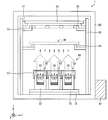
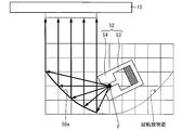
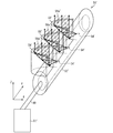
- FIG. 1 is a schematic diagram of a vapor deposition apparatus 1 according to the present embodiment.
- the insulating substrate 111 in FIG. 10 is an example of the deposition target substrate 10 in FIG. 1.
- the vapor deposition apparatus 1 is an apparatus that deposits vapor deposition particles on a predetermined region (hereinafter referred to as a vapor deposition film formation target region) of the deposition target substrate 10, and vapor deposition particles that inject the vapor deposition particles toward the deposition target substrate 10. It has the injection
- the vapor deposition film formation target surface in the claims is a surface having a vapor deposition film formation target region.
- the vapor deposition mask 20 and the vapor deposition particle injection mechanism 84 are disposed to face each other with a certain gap (gap) (that is, separated by a certain distance).
- gap a certain gap
- the vapor deposition mask 20 is made of, for example, a metal member.
- the vapor deposition mask 20 is a rectangular (band-shaped) vapor deposition mask in which at least one side is formed shorter than the width of the vapor deposition film formation target region of the deposition target substrate 10.
- the vapor deposition mask 20 has an opening (through hole) 21 corresponding to a film formation pattern to be formed on the film formation substrate 10.
- the opening 21 has a strip shape
- the vapor deposition mask 20 has a stripe-shaped opening pattern in which a plurality of the openings 21 are arranged in one direction (here, the long side direction of the vapor deposition mask 20).
- the openings 21 are formed so as to be long in the short side direction of the vapor deposition mask 20, and a plurality of openings 21 are provided side by side in the long side direction of the vapor deposition mask 20.
- the deposition target substrate 10 is scanned in the short side direction (scanning direction) of the vapor deposition mask 20 while fixing the relative position between the vapor deposition mask 20 and the vapor deposition particle injection mechanism 84. As a result, a predetermined stripe-shaped vapor deposition pattern is formed in the vapor deposition film formation target region of the deposition target substrate 10.
- the deposition mask 20 and the vapor deposition particle ejection mechanism 84 are fixed to the deposition substrate 10 while the relative position relationship between the vapor deposition mask 20 and the vapor deposition particle ejection mechanism 84 is maintained with the deposition substrate 10 fixed. You may make it move. Alternatively, both the deposition target substrate 10, the vapor deposition mask 20, and the vapor deposition particle injection mechanism 84 may be moved.
- the present invention is not limited to a vapor deposition apparatus of a type that deposits vapor deposition particles on the film formation substrate 10 by moving at least one of the film formation substrate 10 and the vapor deposition mask 20 relative to the other.
- the deposition mask 20 has an area equal to or larger than the deposition film formation target region of the deposition target substrate 10 and can be applied to a deposition apparatus in which the deposition target substrate 10 and the deposition mask 20 are fixed. Is possible.
- the vapor deposition mask 20 having the above configuration can be omitted when a solid pattern is formed on the deposition target substrate 10.
- the vapor deposition particle injection mechanism 84 is disposed below the film formation substrate 10, and the film formation substrate 10 is held with the vapor deposition film formation target region facing downward.
- the vapor deposition particle injection mechanism 84 deposits vapor deposition particles on the vapor deposition film formation target region of the deposition target substrate 10 from below through the opening 21 of the vapor deposition mask 20.
- the vapor deposition particle injection mechanism 84 includes a plurality of crucibles 50.
- the plurality of crucibles 50 are arranged in a line along the arrangement direction of the openings 21 of the vapor deposition mask 20.
- the plurality of crucibles 50 have substantially the same configuration, and have an injection port 86 for injecting (scattering) vapor deposition particles on the surface facing the vapor deposition mask 20.
- the crucible 50 is installed such that the injection port 86 faces the opening 21 of the vapor deposition mask 20.
- the injection ports 86 of the crucible 50 are arranged in a line along the direction in which the openings 21 of the vapor deposition mask 20 are arranged in a state of facing the openings 21 of the vapor deposition mask 20.
- the relative positions of the vapor deposition mask 20 and each crucible 50 are fixed. That is, the gap between the surface of the crucible 50 where the injection port 86 is formed and the vapor deposition mask 20 is always kept constant, and the opening 21 of the vapor deposition mask 20 and the injection port 86 of the crucible 50 The relative position of is fixed.
- the injection port 86 of the crucible 50 is disposed so as to be positioned at the center of the opening 21 of the vapor deposition mask 20 when the vapor deposition mask 20 is viewed from the back surface of the deposition target substrate 10 (that is, in plan view). Is preferred.
- FIG. 2 is a diagram showing a specific configuration of the vapor deposition apparatus 1.
- the vapor deposition apparatus 1 includes a chamber 80 and a vacuum pump mechanism 81 as a casing. Except for the vacuum pump mechanism 81, components of the vapor deposition apparatus 1 including the vapor deposition mask 20 and the vapor deposition particle injection mechanism 84 are accommodated in the chamber 80. The deposition target substrate 10 is also set in the chamber 80.
- the vacuum pump mechanism 81 sets the inside of the chamber 80 to a vacuum state (for example, 1.0 ⁇ 10 ⁇ 4 Pa or less). Specifically, the vacuum pump mechanism 81 exhausts the inside of the chamber 80 to a vacuum state via an exhaust port (not shown) provided in the chamber 80 in order to keep the inside of the chamber 80 in a vacuum state during vapor deposition.
- a vacuum state for example, 1.0 ⁇ 10 ⁇ 4 Pa or less.
- the vapor deposition apparatus 1 includes a frame 60, a movable support 61, a fixed support 62, a shutter 40, a movable support 64, a support base 70, and an actuator 75. Have.
- the frame 60 is erected in the chamber 80 and supports the movable support portion 61, the fixed support portion 62, and the movable support portion 64.
- the movable support 61 is supported by the frame 60 at the highest position, and the movable support 64 is supported at the lowest position.
- the movable support unit 61 supports the deposition target substrate 10 in a horizontal posture.
- the movable support portion 61 can be moved in the X-axis direction (the front side of the drawing in FIG. 2) by an unillustrated drive portion (an example of a drive portion in claims) composed of a stepping motor, a roller, a gear, and the like. It has become.
- the drive unit drives the movable support unit 61, the deposition target substrate 10 moves in the X-axis direction.
- the fixed support part 62 supports the vapor deposition mask 20 in a horizontal posture.
- the shutter 40 is a member for blocking the vapor deposition particles ejected from each crucible 50 of the vapor deposition particle ejection mechanism 84 from reaching the deposition target substrate 10.
- a region of the deposition target substrate 10 where a vapor deposition film is not required hereinafter referred to as a vapor deposition film formation unnecessary region
- the shutter 40 is moved to each crucible 50 of the vapor deposition particle injection mechanism 84.
- the movable support part 64 supports the shutter 40.
- the movable support portion 64 can be moved in the X-axis direction (the front side in the drawing of FIG. 1) by a drive unit similar to the movable support portion 61.
- the drive unit drives the movable support unit 64, the shutter 40 moves in the X-axis direction.
- the support base 70 is placed on an actuator 75 installed on the bottom surface of the chamber 80 and supports the vapor deposition particle injection mechanism 84.
- the actuator 75 moves the support base 70 in the X-axis direction.
- the plurality of crucibles 50 constituting the vapor deposition particle injection mechanism 84 are directions perpendicular to both the relative movement direction (X-axis direction) of the deposition target substrate 10 and the normal direction (Z-axis direction) of the deposition target substrate 10. It is arranged along (Y-axis direction).
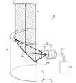
- FIG. 3 is a diagram showing an internal configuration of the crucible 50.
- the crucible 50 has a storage container 51 and an injection container 52.
- the storage container 51 and the injection container 52 are connected via a pipe 55.
- the storage container 51 a solid or liquid vapor deposition material is stored.
- the storage container 51 can be heated by a heater not shown.
- the temperature of the storage container 51 is the temperature at which the vapor deposition material evaporates into vapor deposition particles when the vapor deposition material stored in the storage container 51 is liquid (evaporation). Temperature).
- the temperature of the storage container 51 is set to a temperature higher than the temperature at which the vapor deposition material sublimates to become vapor deposition particles (sublimation temperature).
- the temperature at which the vapor deposition material vaporizes and becomes vapor deposition particles is defined as “vapor deposition particle generation temperature”.
- the vapor deposition material stored in the storage container 51 is vaporized into vapor deposition particles, regardless of whether the vapor deposition material is solid or liquid.
- the vapor deposition particles generated in the storage container 51 are supplied to the injection container 52 via the pipe 55.
- the vapor deposition particle injection mechanism 84 is configured such that vapor deposition particles from the crucible 50 are perpendicularly incident on the deposition target substrate 10. That is, the vapor deposition particle injection mechanism 84 injects a vapor deposition flow parallel to the normal direction of the deposition target substrate 10 from the crucible 50.
- FIG. 4 is an exploded perspective view showing the configuration of the injection container 52.
- the injection container 52 corresponds to a vapor deposition particle injection member, and includes a vapor deposition particle storage member 53 and an injection nozzle member 54. These two members 53 and 54 are joined by, for example, screw machining. It is preferable that the temperature of the vapor deposition particle storage member 53 and the injection nozzle member 54 can be adjusted independently.
- the vapor deposition particle storage member 53 is in the form of a cylindrical container for storing vapor deposition particles in this embodiment.
- the vapor deposition particle storage member 53 of the injection container 52 is connected to the storage container 51 via a pipe 55, and the vapor deposition particles supplied from the storage container 51 are supplied to the vapor deposition particle storage member 53 via the pipe 55. Is done.
- the vapor deposition particle storage member 53 temporarily stores the vapor deposition particles supplied from the storage container 51.
- the injection nozzle member 54 is a member in which an injection port 54a and a rotation inclined surface 54b are formed.
- the rotationally inclined surface 54b is a conical surface, and the conical shape formed by the rotationally inclined surface 54b is set to a shape that improves the utilization efficiency of the vapor deposition material (vapor deposition particles). Is preferred.
- the injection port 54a is provided at the apex of the conical shape formed by the rotation inclined surface 54b.
- the conical shape formed by the rotationally inclined surface 54b has as many vapor deposition particles as possible to be ejected from the injection port 54a, and more preferably, all the vapor deposition particles reach the reflection surface 56a (reflection region) of the reflection member 56 described later.
- the radiation shape is set so as to spread from the exit port 54a at such a radiation angle.
- the crucible 50 includes a reflection member 56 in addition to the storage container 51 and the injection container 52. 2 and 3, the case surrounding the storage container 51, the injection container 52, and the reflection member 56 and the injection port 86 formed on the upper surface of the case are not shown.
- the reflection member 56 has a reflection surface 56 a that reflects the vapor deposition particles emitted from the injection nozzle member 54 toward the vapor deposition film formation target surface of the deposition target substrate 10.
- the reflecting member 56 is installed so that the reflecting surface 56 a faces the injection nozzle member 54 in the crucible 50.
- the relative positional relationship between the reflecting member 56 and the crucible 50 will be described later.
- the temperature of at least the reflecting surface 56a of the reflecting member 56 is controlled by the reflecting member temperature control unit 57 shown in FIG.
- the temperature of at least the reflection surface 56a of the reflection member 56 is set to a temperature higher than the evaporation temperature (deposition particle generation temperature) when vapor deposition particles are generated by evaporating a liquid vapor deposition material in the storage container 51.
- the vapor deposition particles are set to a temperature higher than the sublimation temperature (vapor deposition particle generation temperature).
- the vapor deposition particles are reflected by the reflection surface 56a. More preferably, the temperature of the reflecting surface 56a is set to a temperature at which the vapor deposition particles are completely elastically reflected.
- the reflection surface 56a is formed in a concave curved surface shape.
- the reflecting surface 56a is formed on a rotating paraboloid (parabolic surface) as an example of a concave curved surface shape.
- the reflection surface 56a is formed on one plane when the paraboloid is divided by a plane passing through the apex and the focal point of the paraboloid or the plane parallel to the plane.
- the injection port 54a formed in the injection nozzle member 54 of the crucible 50 is disposed at the position of the focal point F of the paraboloid of revolution.
- FIG. 5 is a diagram for explaining the parabolic principle
- FIG. 6 is a diagram for explaining the function of the reflecting surface 56a in the present embodiment.
- the position of the injection port 54a is defined using this parabola principle. That is, as shown in FIG. 6, the exit port 54a is provided at the focal position of the reflecting surface 56a that is a paraboloid of revolution. Thereby, the reflective surface 56a injects vapor deposition particles in parallel to the normal direction (Z-axis direction) of the deposition target substrate 10.
- the vapor deposition material is vaporized into particles by heating in the storage container 51 of the crucible 50, and the vapor deposition particles are supplied to the injection container 52 of the crucible 50.
- the vapor deposition particles supplied to the injection container 52 are temporarily stored in the vapor deposition particle storage member 53 of the injection container 52 and appropriately discharged from the injection port 54a of the injection nozzle member 54 at a fixed radiation angle.
- the temperature of the reflection surface 56a is set to a predetermined temperature, preferably a temperature at which the vapor deposition particles are completely elastically reflected, so that the vapor deposition particles do not adhere to the reflection surface 56a and are reflected by the reflection surface 56a (including complete elastic reflection). Is done.
- the shape of the reflecting surface 56a is a paraboloid of revolution
- the injection port 54a of the injection nozzle member 54 is disposed at the position of the focal point F of the paraboloid of revolution. Therefore, the vapor deposition particles reflected by the reflecting surface 56 a pass through the injection port 86 toward the vapor deposition mask 20 while being parallel to the normal direction (Z-axis direction) of the deposition target substrate 10.
- the vapor deposition particles that have passed through the opening 21 of the vapor deposition mask 20 reach the vapor deposition film formation target region of the deposition target substrate 10, the vapor deposition particles are vapor deposited on the vapor deposition film formation target region.
- a member that constitutes a vapor deposition source (evaporation particle injection source) in the flow region of the vapor deposition particles between the reflecting member 56 and the deposition target substrate 10. Since the entire structure is disposed, the vapor deposition source component can hinder the flow of the vapor deposition particles.
- the vapor deposition particles are blocked by the vapor deposition source component, and accordingly, an area where the vapor deposition amount is smaller than the surrounding area or an area where no vapor deposition is performed (hereinafter referred to as a shadow area) is generated on the deposition target substrate 10.
- a shadow area an area where the vapor deposition amount is smaller than the surrounding area or an area where no vapor deposition is performed
- the injection container 52 since at least a part of the injection container 52 is installed outside the flow area X of the vapor deposition particles between the reflective surface 56a and the vapor deposition film formation target region, the reflective surface 56a The injection container 52 does not obstruct the flow of the vaporized particles reflected and collimated (vapor deposition flow). As a result, it is possible to prevent or suppress the situation where the film thickness of the vapor deposition film in the vapor deposition film formation target region becomes non-uniform.
- the vapor deposition particles adhere to the injection container 52, the vapor deposition material is not effectively used by the adhering amount. However, in this embodiment, the vapor deposition particles adhere to the injection container 52 and the storage container 51. Since this is avoided, it is also possible to avoid a situation in which the effective utilization rate of the vapor deposition material (a ratio representing how much the vapor deposition material has been effectively utilized without wasting it) is reduced.
- the effective utilization rate of the vapor deposition material is expressed by, for example, “amount of vapor deposition particles vapor deposited on the deposition target substrate 10 / amount of vapor deposition particles injected from the injection container 52”.
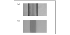
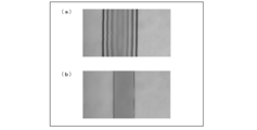
- the inventor of the present application sets the separation distance between the silicon film formation substrate 10 and the vapor deposition mask 20 to 1 mm, and forms a 100 nm vapor deposition film on the film formation substrate 10 with an Alq3 single film. And the vapor deposition apparatus 1 which concerns on this embodiment, respectively, and compared both vapor deposition films. The results of observation with an optical microscope are shown in FIG.
- the film thickness of the film formation pattern was formed evenly over the entire area of the film formation target region of the film formation substrate 10. As a result, it is possible to form a panel with higher display quality than in the prior art.
- the vapor deposition particle storage member 53 that stores the vapor deposition particles is provided corresponding to the injection nozzle member 54.
- the present invention is not limited to this, and a single space for storing the vapor deposition particles is used. You may comprise so that vapor deposition particle
- grains may be distributed to each injection nozzle member. Hereinafter, this specific configuration will be described.
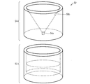
- FIG. 12 is a perspective view schematically showing the external configuration of the crucible 50 ′ according to the present embodiment
- FIG. 13 is a plan view schematically showing the external configuration of the crucible 50 ′.
- the crucible 50 includes a plurality of injection containers 52 and a plurality of reflecting members 56.
- the crucible 50 ′ is a single injection container instead of the plurality of injection containers 52 in the crucible 50 according to the first embodiment. 52 '.
- the crucible 50 ' according to the present embodiment is provided with a plurality of reflecting members 56'.
- the arrangement of the reflection member 56 ' is the same as the arrangement of the reflection member 56 of each crucible 50 in the first embodiment.
- the injection container 52 ′ has an injection nozzle member 54 ′ for injecting vapor deposition particles corresponding to each reflection member 56 ′.
- the crucible 50 ′ has a single storage container 51 ′, and the storage container 51 ′ is connected to the injection container 52 ′ via a pipe 90.
- the storage container 51 ' has a function similar to that of the storage container 51 in the first embodiment.
- the injection container 52 ′ has a space S for temporarily storing the vapor deposition particles supplied from the storage container 51 ′, and the space S is shared by the plurality of injection nozzle members 54 ′. It has become.
- the vapor deposition particles supplied to the space S are ejected from the ejection nozzle member 54 'to the reflecting member 56'.
- the injection container 52 ′ in the present embodiment constitutes the vapor deposition particle injection member in the claims.
- the injection container 52 ′ shown in FIGS. 12 and 13 has a long shape in the arrangement direction of the injection nozzle members 54 ′ in accordance with the plurality of injection nozzle members 54 arranged in one direction. It has a configuration.
- the connection portion between the injection container 52 ′ and the pipe 90, the injection position Due to this positional relationship, it is possible to suppress the occurrence of unevenness in the injection amount of the vapor deposition particles between the injection nozzle members 54 ′.
- the nozzle diameter of the injection nozzle member 54 ′ may be corrected according to the film formation amount for each injection nozzle member 54 ′ obtained by a previously conducted experiment, and the nozzle diameter between the injection nozzle members 54 ′ may be corrected. May be different.
- the injection container 52 ′ and the pipe 90 are connected at a plurality of suitable locations.
- the part on the tank member 53 'side of the pipe 90 may be branched into a plurality of pipes, and each branch part may be connected to an appropriate position of the injection container 52'.
- a plurality of storage containers 51 ′ may be provided, and each storage container 51 ′ and the injection container 52 ′ may be connected by a plurality of pipes 90.
- the injection container 52 ′ is outside the flow region X of the vapor deposition particles between the reflection surface of the reflection member 56 ′ and the vapor deposition film formation target surface of the deposition target substrate (not shown). is set up.
- the injection container 52 ′, the reflection member 56 ′, and the pipe 90 it is desirable to set the injection container 52 ′, the reflection member 56 ′, and the pipe 90 to a temperature higher than the vapor deposition particle generation temperature.
- the storage container 51 ′ may be provided inside the chamber 80 or outside the chamber 80. If the storage container 51 ′ is installed outside the chamber 80, the structure of the chamber 80 can be simplified, and the temperature control of the vapor deposition material is facilitated.
- FIG. 14 is a diagram showing the vapor deposition apparatus 2 according to the present embodiment.
- the same members as those in the above-described embodiment are denoted by the same reference numerals, and differences from the above-described embodiment will be mainly described.
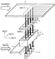
- the vapor deposition apparatus 2 shown in FIG. 14 includes a limiting plate 30 and a fixed support portion 63 in addition to the constituent members of the vapor deposition apparatus 1 including the crucible 50 according to the first embodiment.
- the fixed support portion 63 is supported by the frame 60 between the fixed support portion 62 and the movable support portion 64. Therefore, the limiting plate 30 is disposed between the vapor deposition mask 20 and the shutter 40 and is fixed at that position.
- FIG. 15 is a perspective view showing the arrangement of the deposition target substrate 10, the vapor deposition mask 20, the limiting plate 30, the shutter 40, and the vapor deposition particle injection mechanism 84 in the vapor deposition apparatus 2.
- the limiting plate 30 has an opening 31 that faces the opening 21 of the vapor deposition mask 20.
- the vapor deposition particle injection mechanism 84 the vapor deposition particles injected from the crucible 50 (the injection port 54 a of the injection nozzle member 54, see FIG. 3) pass through the opening 31 of the limiting plate 30 and the opening 21 of the vapor deposition mask 20. A flow path for vapor deposition particles reaching the deposition target substrate 10 is formed.
- the vapor deposition particles reflected by the reflection surface 56a (see FIG. 3) of the reflection member 56 may include vapor deposition particles that are not completely parallel to the normal direction of the deposition target substrate 10. is there.
- the limiting plate 30 removes some of the vapor deposition particles that are not completely parallel as unnecessary vapor deposition particles from the vapor deposition flow injected into the vapor deposition film formation target region of the deposition target substrate 10.
- the limiting plate 30 is set to a temperature lower than the vapor deposition particle generation temperature by a temperature control unit (not shown). In addition, you may provide the cooling mechanism which cools the restriction
- the blurring of the film formation pattern formed on the film formation substrate 10 can be further reduced.
- the inventor of the present application sets the separation distance between the silicon deposition substrate 10 and the vapor deposition mask 20 to 1 mm, and forms a 100 nm Alq3 vapor deposition film (single film) on the deposition target substrate 10.
- Each was formed by the apparatus and the vapor deposition apparatus according to the present example, and both vapor deposition films were compared. The results of observation with an optical microscope are shown in FIG.
- the inventor of the present application produced a large blur of the film formation pattern as shown in FIG. As shown in FIG. 16B, it was confirmed that the pattern blur was improved.
- the vapor deposition film can be formed over the entire region where the vapor deposition film is to be formed on the deposition target substrate 10 without the occurrence of film thickness unevenness in the film formation pattern. As a result, a panel with high display quality can be formed.
- the vapor deposition apparatus in each of the above embodiments was configured to up-deposit (deposit up) vapor deposition particles on the deposition target substrate from below to above through the opening of the vapor deposition mask.
- a deposition apparatus for down deposition (down deposition) in which vapor deposition particles are vapor-deposited on a film formation substrate from the upper side to the lower side through an opening of the vapor deposition mask,
- the present invention can also be applied to a vapor deposition apparatus that causes vapor deposition particles to be side-positioned (side deposit) from the side on the film formation substrate.
- the configuration in which the injection nozzle member is provided one-dimensionally is shown. Therefore, the injection nozzle member may be provided two-dimensionally.
- the number of the injection nozzle members 54 is three, but the number is not limited to this number, and any number is possible. In the case of a vapor deposition apparatus that relatively moves the deposition target substrate 10 and the deposition mask 20 in one direction, the larger the number of injection nozzle members 54, the larger the deposition target substrate 10 can be handled.
- the reflecting surface of the reflecting member is a rotating paraboloid, but it need not be a complete rotating paraboloid, and may be a concave curved surface close to the rotating paraboloid. Further, a part of the reflecting surface may be a paraboloid of revolution.
- the injection port is preferably provided outside the basin.
- the injection port is preferably provided outside the basin.
- the whole of the vapor deposition particle injection member is located outside the basin.
- the entire vapor-deposited particle injection member is located outside the basin.
- the reflecting surface is a rotating paraboloid, and the injection port is provided at a focal position of the rotating paraboloid.
- the reflection surface is a paraboloid of revolution, and the exit is provided at a focal position of the paraboloid of revolution.
- the traveling direction of the vapor deposition particles reflected by the reflecting member can be made parallel to the normal direction of the deposition target substrate.
- parallel includes not only a case where the film is completely parallel to the normal direction of the film formation substrate but also a direction that can be regarded as parallel to the normal direction of the film formation substrate.
- a plurality of the injection ports are provided on a plane parallel to the deposition film formation target surface.
- a plurality of the injection ports are provided on a plane parallel to the vapor deposition film formation target surface.
- the time required to form the vapor deposition film on the surface on which the vapor deposition film is to be formed can be shortened as compared with the case where there is one injection port.
- the temperature of the reflecting surface is higher than the vapor generation particle generation temperature at which the vapor deposition material of the vapor deposition particles vaporizes.
- the temperature of the reflecting surface is higher than a vapor generation particle generation temperature at which the vapor deposition material of the vapor deposition particles vaporizes.
- the vapor deposition particles are completely elastically reflected on the reflecting surface. be able to.
- a vapor deposition apparatus includes any one of the above crucibles.
- the vapor deposition apparatus includes a drive unit that relatively moves the vapor deposition film formation target surface and the crucible.
- the vapor deposition method according to the embodiment of the present invention includes a moving step of relatively moving the vapor deposition film formation target surface, the ejection port, and the reflection surface when vapor deposition particles are ejected.
- the deposition substrate is large, when forming a deposition film with the deposition substrate stationary, a deposition source area that is almost the same size as the deposition substrate is required, and a large number of crucibles are required. Thus, there is a problem that the device cost increases.
- the number of crucibles can be reduced by adopting the above configuration. Thereby, apparatus cost can be reduced.
- the vapor deposition apparatus which concerns on embodiment of this invention is provided with the vapor deposition mask for forming the film-forming pattern of the said vapor deposition film.
- the vapor deposition method according to the embodiment of the present invention includes a vapor deposition mask preparation step of preparing a vapor deposition mask for forming a deposition pattern of the vapor deposition film before the injection step.
- the pixel since the parallelized vapor deposition flow passes through the vapor deposition mask and reaches the vapor deposition film formation target surface, by appropriately setting the size of the vapor deposition particle passage region in the vapor deposition mask, the pixel It becomes possible to form a pattern with a fine unit.
- the vapor deposition apparatus includes a limiting plate for bringing the traveling direction of the vapor deposition particles close to the normal direction of the deposition target substrate.
- the vapor deposition method according to an embodiment of the present invention includes a limiting plate preparation step of preparing a limiting plate for bringing the traveling direction of the vapor deposition particles close to the normal direction of the film formation substrate before the injection step. It is preferable to provide.
- the traveling direction of the vapor deposition particles reflected by the reflecting member further approaches the normal direction of the film formation substrate, it is possible to further parallelize the vapor deposition flow.
- the crucible according to the present invention can be suitably used for, for example, a manufacturing apparatus and a manufacturing method of an organic EL display device used for a film forming process of an organic film in the organic EL display device.
Abstract
被成膜基板(10)の蒸着膜形成対象領域に蒸着膜を形成するための蒸着粒子を射出する射出口(54a)を備えた射出用容器(52)と、射出口(54a)から射出された蒸着粒子を前記蒸着膜形成対象面に向けて反射する凹曲形状の反射面(56a)とを坩堝(50)に備え、射出用容器(52)を、その少なくとも一部が、反射面(56a)と前記蒸着膜形成対象領域との間における蒸着粒子の流域Xの外部に位置するように設置した。
Description
本発明は、被成膜基板に蒸着粒子のパターンを成膜するための蒸着技術に関するものである。
近年、様々な商品や分野でフラットパネルディスプレイが活用されており、フラットパネルディスプレイのさらなる大型化、高画質化、低消費電力化が求められている。
そのような状況下、有機材料の電界発光(Electroluminescence;以下、「EL」と記す)を利用した有機EL素子を備えた有機EL表示装置は、全固体型で、低電圧駆動、高速応答性、自発光性等の点で優れたフラットパネルディスプレイとして、高い注目を浴びている。
有機EL表示装置は、例えば、TFT(薄膜トランジスタ)が設けられたガラス基板等からなる基板上に、TFTに接続された有機EL素子が設けられた構成を有している。
有機EL素子は、低電圧直流駆動による高輝度発光が可能な発光素子であり、第1電極、有機EL層、および第2電極が、この順に積層された構造を有している。そのうち、第1電極はTFTと接続されている。また、第1電極と第2電極との間には、上記有機EL層として、正孔注入層、正孔輸送層、電子ブロッキング層、発光層、正孔ブロッキング層、電子輸送層、電子注入層等を積層させた有機層が設けられている。
フルカラーの有機EL表示装置では、一般的に、赤(R)、緑(G)、青(B)の各色の発光層を備えた有機EL素子がサブ画素として基板上に配列形成される。TFTを用いて、これら有機EL素子を選択的に所望の輝度で発光させることによりカラー画像表示を行う。
有機EL表示装置を製造するためには、各色に発光する有機発光材料からなる発光層を有機EL素子ごとに所定パターンで形成する必要がある。また、有機EL素子ごとにパターン形成が必要ない層については、有機EL素子で構成される画素領域全面に対して、一括して薄膜形成を行う。
発光層を所定パターンで形成する方法としては、例えば、真空蒸着法、インクジェット法、レーザ転写法が知られている。例えば、低分子型有機EL表示装置(OLED)では、真空蒸着法が用いられることが多い。
真空蒸着法では、所定パターンの開口が形成されたマスク(蒸着マスクとも称される)が使用される。マスクが密着固定された基板の被蒸着面を蒸着源に対向させる。そして、蒸着源からの蒸着粒子(成膜材料)を、マスクの開口を通して被蒸着面に蒸着させることにより、所定パターンの薄膜が形成される。蒸着は発光層の色ごとに行われる(これを「塗り分け蒸着」という)。
下記特許文献1には、蒸発物質の蒸発源201と、蒸発源201に対して蒸発物質Vaを蒸着すべき蒸着領域Rと反対側に設置され、蒸発源201から射出された蒸発物質Vaを反射する反射部材202とを備えた蒸着装置200が開示されている。また、同特許文献1の反射部材202は、断面が凹状の曲線をなし前記断面に垂直な方向に延びるものとされ、蒸発源201が前記曲線の焦点近傍位置に配置されている点が記載されている。これにより、蒸発物質Vaの進行方向が蒸着領域Rの法線にほぼ平行となるので、蒸着膜の厚さの均一化を図ることができる。
前記特許文献1にあっては、蒸発源201を構成する部材(以下、蒸着源構成部材という)全体が、反射された蒸発物質の流域内に設置されている。そのため、蒸着源構成部材によって蒸着流が乱れ、蒸着膜を形成する対象面における蒸着膜の膜厚分布が均一とならなかったり、蒸着材料が蒸着膜形成対象面に蒸着する割合が低下したりするという問題が生じることが考えられる。
本発明は、上記問題点に鑑みてなされたものであり、蒸着率の低下を可及的に防止することのできる坩堝、蒸着装置、蒸着方法及び有機エレクトロルミネッセンス表示装置の製造方法を提供することを目的とする。
上記目的を達成するために、本発明に係る坩堝は、被成膜基板の蒸着膜形成対象面に蒸着膜を形成するための蒸着粒子を射出する射出口を備えた蒸着粒子射出部材と、前記射出口から射出された蒸着粒子を前記蒸着膜形成対象面に向けて反射する凹曲形状の反射面とを備え、前記蒸着粒子射出部材は、少なくとも一部が、前記反射面と前記蒸着膜形成対象面との間における蒸着粒子の流域の外部に位置するように設置されていることを特徴とするものである。
また、本発明に係る蒸着方法は、被成膜基板の蒸着膜形成対象面に蒸着膜を形成するための蒸着方法であって、蒸着粒子を蒸着粒子射出部材の射出口から射出する射出工程と、前記射出口から射出された蒸着粒子を凹曲形状の反射面によって前記蒸着膜形成対象面に向けて反射する反射工程とを備え、前記蒸着粒子射出部材は、少なくとも一部が、前記反射面と前記蒸着膜形成対象面との間における蒸着粒子の流域の外部に位置するように設置されていることを特徴とするものである。
これらの発明によれば、前記蒸着粒子射出部材は、少なくとも一部が前記反射面と前記蒸着膜形成対象面との間における蒸着粒子の流域の外部に位置するように設置されるので、蒸着粒子射出部材によって蒸着粒子の流れ(以下、蒸着流という)が乱れ、前記蒸着膜形成対象面における蒸着膜の膜厚が均一にならなくなるという事態を可及的に防止することができる。
本発明に係る有機エレクトロルミネッセンス表示装置の製造方法は、TFT基板上に第1電極を作製するTFT基板・第1電極作製工程と、前記TFT基板上に少なくとも発光層を含む有機層を蒸着する有機層蒸着工程と、第2電極を蒸着する第2電極蒸着工程と、前記有機層および第2電極を含む有機エレクトロルミネッセンス素子を封止部材で封止する封止工程とを有する有機エレクトロルミネッセンス表示装置の製造方法であって、前記有機層蒸着工程、前記第2電極蒸着工程、および前記封止工程の少なくともいずれかの工程は、前記何れかの蒸着方法の各工程を有することを特徴とするものである。
この発明によれば、一定の蒸着率を得つつ、膜厚分布が均一化されるので、表示ムラの少ない有機エレクトロルミネッセンス表示装置を実現することができる。
本発明に係る坩堝は、被成膜基板の蒸着膜形成対象面に蒸着膜を形成するための蒸着粒子を射出する射出口を備えた蒸着粒子射出部材と、前記射出口から射出された蒸着粒子を前記蒸着膜形成対象面に向けて反射する凹曲形状の反射面とを備え、前記蒸着粒子射出部材は、少なくとも一部が、前記反射面と前記蒸着膜形成対象面との間における蒸着粒子の流域の外部に位置するように設置されている。
また、本発明に係る蒸着方法は、被成膜基板の蒸着膜形成対象面に蒸着膜を形成するための蒸着方法であって、蒸着粒子を蒸着粒子射出部材の射出口から射出する射出工程と、前記射出口から射出された蒸着粒子を凹曲形状の反射面によって前記蒸着膜形成対象面に向けて反射する反射工程とを備え、前記蒸着粒子射出部材は、少なくとも一部が、前記反射面と前記蒸着膜形成対象面との間における蒸着粒子の流域の外部に位置するように設置されている。
これにより、前記蒸着粒子射出部材は、少なくとも一部が前記反射面と前記蒸着膜形成対象面との間における蒸着粒子の流域の外部に位置するように設置されるので、蒸着粒子射出部材によって蒸着流が乱れ、前記蒸着膜形成対象面における蒸着膜の膜厚が均一にならなくなるという事態を可及的に防止又は抑制することができる。
以下、本発明の実施形態について、詳細に説明する。
〔実施形態1〕
本発明の第1の実施形態について図1~図16に基づいて説明すれば以下のとおりである。
本発明の第1の実施形態について図1~図16に基づいて説明すれば以下のとおりである。
本実施の形態では、本実施の形態にかかる蒸着装置を用いた蒸着方法の一例として、TFT基板側から光を取り出すボトムエミッション型でRGBフルカラー表示の有機EL表示装置の製造方法を例に挙げて説明する。
まず、上記有機EL表示装置の全体構成について以下に説明する。
図8は、RGBフルカラー表示の有機EL表示装置の概略構成を示す断面図である。また、図9は、図8に示す有機EL表示装置を構成する画素の構成を示す平面図であり、図10は、図9に示す有機EL表示装置におけるTFT基板のA-A線矢視断面図である。
図8に示すように、本実施の形態で製造される有機EL表示装置100は、TFT112(図10参照)が設けられたTFT基板110上に、TFT112に接続された有機EL素子120、接着層130、封止基板140が、この順に設けられた構成を有している。
図8に示すように、有機EL素子120は、該有機EL素子120が積層されたTFT基板110を、接着層130を用いて封止基板140と貼り合わせることで、これら一対の基板(TFT基板110、封止基板140)間に封入されている。
上記有機EL表示装置100は、このように有機EL素子120がTFT基板110と封止基板140との間に封入されていることで、有機EL素子120への酸素や水分の外部からの浸入が防止されている。
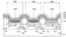
TFT基板110は、図10に示すように、支持基板として、例えばガラス基板等の透明な絶縁基板111を備えている。絶縁基板111上には、図9に示すように、水平方向に敷設された複数のゲート線と、垂直方向に敷設され、ゲート線と交差する複数の信号線とからなる複数の配線114が設けられている。ゲート線には、ゲート線を駆動する図示しないゲート線駆動回路が接続され、信号線には、信号線を駆動する図示しない信号線駆動回路が接続されている。
有機EL表示装置100は、フルカラーのアクティブマトリクス型の有機EL表示装置であり、絶縁基板111上には、これら配線114で囲まれた領域に、それぞれ、赤(R)、緑(G)、青(B)の各色の有機EL素子120からなる各色のサブ画素102R・102G・102Bが、マトリクス状に配列されている。
すなわち、これら配線114で囲まれた領域が1つのサブ画素(ドット)であり、サブ画素毎にR、G、Bの発光領域が画成されている。
画素(すなわち、1画素)は、赤色の光を透過する赤色のサブ画素102R、緑色の光を透過する緑色のサブ画素102G、青色の光を透過する青色のサブ画素102Bの、3つのサブ画素102R・102G・102Bによって構成されている。
各サブ画素102R・102G・102Bには、各サブ画素102R・102G・102Bにおける発光を担う各色の発光領域として、ストライプ状の各色の発光層123R・123G・123Bによって覆われた開口部115R・115G・115Bがそれぞれ設けられている。
これら発光層123R・123G・123Bは、各色毎に、蒸着によりパターン形成されている。なお、開口部115R・115G・115Bについては後述する。
これらサブ画素102R・102G・102Bには、有機EL素子120における第1電極121に接続されたTFT112がそれぞれ設けられている。各サブ画素102R・102G・102Bの発光強度は、配線114およびTFT112による走査および選択により決定される。このように、有機EL表示装置100は、TFT112を用いて、有機EL素子120を選択的に所望の輝度で発光させることにより画像表示を実現している。
次に、上記有機EL表示装置100におけるTFT基板110および有機EL素子120の構成について詳述する。
まず、TFT基板110について説明する。
TFT基板110は、図10に示すように、ガラス基板等の透明な絶縁基板111上に、TFT112(スイッチング素子)、層間膜113(層間絶縁膜、平坦化膜)、配線114、エッジカバー115がこの順に形成された構成を有している。
上記絶縁基板111上には、配線114が設けられているとともに、各サブ画素102R・102G・102Bに対応して、それぞれTFT112が設けられている。なお、TFTの構成は従来よく知られている。したがって、TFT112における各層の図示並びに説明は省略する。
層間膜113は、各TFT112を覆うように、上記絶縁基板111上に、上記絶縁基板111の全領域に渡って積層されている。
層間膜113上には、有機EL素子120における第1電極121が形成されている。
また、層間膜113には、有機EL素子120における第1電極121をTFT112に電気的に接続するためのコンタクトホール113aが設けられている。これにより、TFT112は、上記コンタクトホール113aを介して、有機EL素子120に電気的に接続されている。
エッジカバー115は、第1電極121のパターン端部で有機EL層が薄くなったり電界集中が起こったりすることで、有機EL素子120における第1電極121と第2電極126とが短絡することを防止するための絶縁層である。
エッジカバー115は、層間膜113上に、第1電極121のパターン端部を被覆するように形成されている。
エッジカバー115には、サブ画素102R・102G・102B毎に開口部115R・115G・115Bが設けられている。このエッジカバー115の開口部115R・115G・115Bが、各サブ画素102R・102G・102Bの発光領域となる。
言い換えれば、各サブ画素102R・102G・102Bは、絶縁性を有するエッジカバー115によって仕切られている。エッジカバー115は、素子分離膜としても機能する。
次に、有機EL素子120について説明する。
有機EL素子120は、低電圧直流駆動による高輝度発光が可能な発光素子であり、第1電極121、有機EL層、第2電極126が、この順に積層されている。
第1電極121は、上記有機EL層に正孔を注入(供給)する機能を有する層である。第1電極121は、前記したようにコンタクトホール113aを介してTFT112と接続されている。
第1電極121と第2電極126との間には、図10に示すように、有機EL層として、第1電極121側から、正孔注入層兼正孔輸送層122、発光層123R・123G・123B、電子輸送層124、電子注入層125が、この順に形成された構成を有している。
なお、上記積層順は、第1電極121を陽極とし、第2電極126を陰極としたものであり、第1電極121を陰極とし、第2電極126を陽極とする場合には、有機EL層の積層順は反転する。
正孔注入層は、発光層123R・123G・123Bへの正孔注入効率を高める機能を有する層である。また、正孔輸送層は、発光層123R・123G・123Bへの正孔輸送効率を高める機能を有する層である。正孔注入層兼正孔輸送層122は、第1電極121およびエッジカバー115を覆うように、上記TFT基板110における表示領域全面に一様に形成されている。
なお、本実施の形態では、上記したように、正孔注入層および正孔輸送層として、正孔注入層と正孔輸送層とが一体化された正孔注入層兼正孔輸送層122を設けた場合を例に挙げて説明する。しかしながら、本実施の形態はこれに限定されるものではない。正孔注入層と正孔輸送層とは互いに独立した層として形成されていてもよい。
正孔注入層兼正孔輸送層122上には、発光層123R・123G・123Bが、エッジカバー115の開口部115R・115G・115Bを覆うように、それぞれ、サブ画素102R・102G・102Bに対応して形成されている。
発光層123R・123G・123Bは、第1電極121側から注入されたホール(正孔)と第2電極126側から注入された電子とを再結合させて光を出射する機能を有する層である。発光層123R・123G・123Bは、それぞれ、低分子蛍光色素、金属錯体等の、発光効率が高い材料で形成されている。
電子輸送層124は、第2電極126から発光層123R・123G・123Bへの電子輸送効率を高める機能を有する層である。また、電子注入層125は、第2電極126から発光層123R・123G・123Bへの電子注入効率を高める機能を有する層である。
電子輸送層124は、発光層123R・123G・123Bおよび正孔注入層兼正孔輸送層122を覆うように、これら発光層123R・123G・123Bおよび正孔注入層兼正孔輸送層122上に、上記TFT基板110における表示領域全面に渡って一様に形成されている。また、電子注入層125は、電子輸送層124を覆うように、電子輸送層124上に、上記TFT基板110における表示領域全面に渡って一様に形成されている。
なお、電子輸送層124と電子注入層125とは、上記したように互いに独立した層として形成されていてもよく、互いに一体化して設けられていてもよい。すなわち、上記有機EL表示装置100は、電子輸送層124および電子注入層125に代えて、電子輸送層兼電子注入層を備えていてもよい。
第2電極126は、上記のような有機層で構成される有機EL層に電子を注入する機能を有する層である。第2電極126は、電子注入層125を覆うように、電子注入層125上に、上記TFT基板110における表示領域全面に渡って一様に形成されている。
なお、発光層123R・123G・123B以外の有機層は有機EL層として必須の層ではなく、要求される有機EL素子120の特性に応じて適宜形成すればよい。また、有機EL層には、必要に応じ、キャリアブロッキング層を追加することもできる。例えば、発光層123R・123G・123Bと電子輸送層124との間にキャリアブロッキング層として正孔ブロッキング層を追加することで、正孔が電子輸送層124に抜けるのを阻止し、発光効率を向上することができる。
上記有機EL素子120の構成としては、例えば、下記(1)~(8)に示すような層構成を採用することができる。
(1)第1電極/発光層/第2電極
(2)第1電極/正孔輸送層/発光層/電子輸送層/第2電極
(3)第1電極/正孔輸送層/発光層/正孔ブロッキング層(キャリアブロッキング層)/電子輸送層/第2電極
(4)第1電極/正孔輸送層/発光層/正孔ブロッキング層/電子輸送層/電子注入層/第2電極
(5)第1電極/正孔注入層/正孔輸送層/発光層/電子輸送層/電子注入層/第2電極
(6)第1電極/正孔注入層/正孔輸送層/発光層/正孔ブロッキング層/電子輸送層/第2電極
(7)第1電極/正孔注入層/正孔輸送層/発光層/正孔ブロッキング層/電子輸送層/電子注入層/第2電極
(8)第1電極/正孔注入層/正孔輸送層/電子ブロッキング層(キャリアブロッキング層)/発光層/正孔ブロッキング層/電子輸送層/電子注入層/第2電極
なお、上記したように、例えば正孔注入層と正孔輸送層とは、一体化されていてもよい。また、電子輸送層と電子注入層とは一体化されていてもよい。
また、有機EL素子120の構成は上記例示の層構成に限定されるものではなく、上記したように、要求される有機EL素子120の特性に応じて所望の層構成を採用することができる。
次に、上記有機EL表示装置100の製造方法について以下に説明する。
図11は、上記有機EL表示装置100の製造工程を工程順に示すフローチャートである。
図11に示すように、本実施の形態にかかる有機EL表示装置100の製造方法は、例えば、TFT基板・第1電極作製工程(S1)、正孔注入層・正孔輸送層蒸着構成(S2)、発光層蒸着工程(S3)、電子輸送層蒸着工程(S4)、電子注入層蒸着工程(S5)、第2電極蒸着工程(S6)、封止工程(S7)を備えている。
以下に、図11に示すフローチャートに従って、図8および図10を参照して上記した各工程について説明する。
但し、本実施の形態に記載されている各構成要素の寸法、材質、形状等はあくまで一実施形態に過ぎず、これによって本発明の範囲が限定解釈されるべきではない。
また、前記したように、本実施形態に記載の積層順は、第1電極121を陽極、第2電極126を陰極としたものであり、反対に第1電極121を陰極とし、第2電極126を陽極とする場合には、有機EL層の積層順は反転する。同様に、第1電極121および第2電極126を構成する材料も反転する。
まず、図10に示すように、公知の技術でTFT112並びに配線114等が形成されたガラス等の絶縁基板111上に感光性樹脂を塗布し、フォトリソグラフィ技術によりパターニングを行うことで、絶縁基板111上に層間膜113を形成する。
上記絶縁基板111としては、例えば厚さが0.7~1.1mmであり、y軸方向の長さ(縦長さ)が400~500mmであり、x軸方向の長さ(横長さ)が300~400mmのガラス基板あるいはプラスチック基板が用いられる。なお、本実施の形態では、ガラス基板を用いた。
層間膜113としては、例えば、アクリル樹脂やポリイミド樹脂等を用いることができる。アクリル樹脂としては、例えば、JSR株式会社製のオプトマーシリーズが挙げられる。また、ポリイミド樹脂としては、例えば、東レ株式会社製のフォトニースシリーズが挙げられる。但し、ポリイミド樹脂は一般に透明ではなく、有色である。このため、図10に示すように上記有機EL表示装置100としてボトムエミッション型の有機EL表示装置を製造する場合には、上記層間膜113としては、アクリル樹脂等の透明性樹脂が、より好適に用いられる。
上記層間膜113の膜厚としては、TFT112による段差を補償することができればよく、特に限定されるものではない。本実施の形態では、例えば、約2μmとした。
次に、層間膜113に、第1電極121をTFT112に電気的に接続するためのコンタクトホール113aを形成する。
次に、導電膜(電極膜)として、例えばITO(Indium Tin Oxide:インジウム錫酸化物)膜を、スパッタ法等により、100nmの厚さで成膜する。
次いで、上記ITO膜上にフォトレジストを塗布し、フォトリソグラフィ技術を用いてパターニングを行った後、塩化第二鉄をエッチング液として、上記ITO膜をエッチングする。その後、レジスト剥離液を用いてフォトレジストを剥離し、さらに基板洗浄を行う。これにより、層間膜113上に、第1電極121をマトリクス状に形成する。
なお、上記第1電極121に用いられる導電膜材料としては、例えば、ITO、IZO(Indium Zinc Oxide:インジウム亜鉛酸化物)、ガリウム添加酸化亜鉛(GZO)等の透明導電材料、金(Au)、ニッケル(Ni)、白金(Pt)等の金属材料、を用いることができる。
また、上記導電膜の積層方法としては、スパッタ法以外に、真空蒸着法、CVD(chemical vapor deposition、化学蒸着)法、プラズマCVD法、印刷法等を用いることができる。
上記第1電極121の厚さとしては特に限定されるものではないが、上記したように、例えば、100nmの厚さとすることができる。
次に、層間膜113と同様にして、エッジカバー115を、例えば約1μmの膜厚でパターニング形成する。エッジカバー115の材料としては、層間膜113と同様の絶縁材料を使用することができる。
以上の工程により、TFT基板110および第1電極121が作製される(S1)。
次に、上記のような工程を経たTFT基板110に対し、脱水のための減圧ベークおよび第1電極121の表面洗浄として酸素プラズマ処理を施す。
次いで、従来の蒸着装置を用いて、上記TFT基板110上に、正孔注入層および正孔輸送層(本実施の形態では正孔注入層兼正孔輸送層122)を、上記TFT基板110における表示領域全面に蒸着する(S2)。
具体的には、表示領域全面が開口したオープンマスクを、TFT基板110に対しアライメント調整を行った後に密着して貼り合わせ、TFT基板110とオープンマスクとを共に回転させながら、蒸着源より飛散した蒸着粒子を、オープンマスクの開口部を通じて表示領域全面に均一に蒸着する。
ここで表示領域全面への蒸着とは、隣接した色の異なるサブ画素間に渡って途切れなく蒸着することを意味する。
正孔注入層および正孔輸送層の材料としては、例えば、ベンジン、スチリルアミン、トリフェニルアミン、ポルフィリン、トリアゾール、イミダゾール、オキサジアゾール、ポリアリールアルカン、フェニレンジアミン、アリールアミン、オキザゾール、アントラセン、フルオレノン、ヒドラゾン、スチルベン、トリフェニレン、アザトリフェニレン、およびこれらの誘導体、ポリシラン系化合物、ビニルカルバゾール系化合物、チオフェン系化合物、アニリン系化合物等の、複素環式または鎖状式共役系のモノマー、オリゴマー、またはポリマー、等が挙げられる。
正孔注入層と正孔輸送層とは、前記したように一体化されていてもよく、独立した層として形成されていてもよい。各々の膜厚としては、例えば、10~100nmである。
本実施の形態では、正孔注入層および正孔輸送層として、正孔注入層兼正孔輸送層122を設けるとともに、正孔注入層兼正孔輸送層122の材料として、4,4’-ビス[N-(1-ナフチル)-N-フェニルアミノ]ビフェニル(α-NPD)を使用した。また、正孔注入層兼正孔輸送層122の膜厚は30nmとした。
次に、上記正孔注入層兼正孔輸送層122上に、エッジカバー115の開口部115R・115G・115Bを覆うように、サブ画素102R・102G・102Bに対応して発光層123R・123G・
123Bをそれぞれ塗り分け形成(パターン形成)する(S3)。
123Bをそれぞれ塗り分け形成(パターン形成)する(S3)。
前記したように、発光層123R・123G・123Bには、低分子蛍光色素、金属錯体等の発光効率が高い材料が用いられる。
発光層123R・123G・123Bの材料としては、例えば、アントラセン、ナフタレン、インデン、フェナントレン、ピレン、ナフタセン、トリフェニレン、アントラセン、ペリレン、ピセン、フルオランテン、アセフェナントリレン、ペンタフェン、ペンタセン、コロネン、ブタジエン、クマリン、アクリジン、スチルベン、およびこれらの誘導体、トリス(8-キノリノラト)アルミニウム錯体、ビス(ベンゾキノリノラト)ベリリウム錯体、トリ(ジベンゾイルメチル)フェナントロリンユーロピウム錯体、ジトルイルビニルビフェニル、等が挙げられる。
発光層123R・123G・123Bの膜厚としては、例えば、10~100nmである。
本実施の形態にかかる蒸着方法並びに蒸着装置は、このような発光層123R・123G・123Bの塗り分け形成(パターン形成)に特に好適に使用することができる。
本実施の形態にかかる蒸着方法並びに蒸着装置を用いた発光層123R・123G・123Bの塗り分け形成については、後で詳述する。
次に、上記した正孔注入層・正孔輸送層蒸着工程(S2)と同様の方法により、電子輸送層124を、上記正孔注入層兼正孔輸送層122および発光層123R・123G・123Bを覆うように、上記TFT基板110における表示領域全面に蒸着する(S4)。
続いて、上記した正孔注入層・正孔輸送層蒸着工程(S2)と同様の方法により、電子注入層125を、上記電子輸送層124を覆うように、上記TFT基板110における表示領域全面に蒸着する(S5)。
電子輸送層124および電子注入層125の材料としては、例えば、トリス(8-キノリノラト)アルミニウム錯体、オキサジアゾール誘導体、トリアゾール誘導体、フェニルキノキサリン誘導体、シロール誘導体等が挙げられる。
具体的には、Alq(トリス(8-ヒドロキシキノリン)アルミニウム)、アントラセン、ナフタレン、フェナントレン、ピレン、アントラセン、ペリレン、ブタジエン、クマリン、アクリジン、スチルベン、1,10-フェナントロリン、およびこれらの誘導体や金属錯体、LiF、等が挙げられる。
前記したように電子輸送層124と電子注入層125とは、一体化されていても独立した層として形成されていてもよい。各々の膜厚としては、例えば、1~100nmである。また、電子輸送層124および電子注入層125の合計の膜厚は、例えば20~200nmである。
本実施の形態では、電子輸送層124の材料にAlqを使用し、電子注入層125の材料には、LiFを使用した。また、電子輸送層124の膜厚は30nmとし、電子注入層125の膜厚は1nmとした。
次に、上記した正孔注入層・正孔輸送層蒸着工程(S2)と同様の方法により、第2電極126を、上記電子注入層125を覆うように、上記TFT基板110における表示領域全面に蒸着する(S6)。
第2電極126の材料(電極材料)としては、仕事関数の小さい金属等が好適に用いられる。このような電極材料としては、例えば、マグネシウム合金(MgAg等)、アルミニウム合金(AlLi、AlCa、AlMg等)、金属カルシウム等が挙げられる。第2電極126の厚さは、例えば50~100nmである。
本実施の形態では、第2電極126としてアルミニウムを50nmの膜厚で形成した。これにより、TFT基板110上に、上記した有機EL層、第1電極121、および第2電極126からなる有機EL素子120を形成した。
次いで、図8に示すように、有機EL素子120が形成された上記TFT基板110と、封止基板140とを、接着層130にて貼り合わせ、有機EL素子120の封入を行った。
上記封止基板140としては、例えば厚さが0.4~1.1mmのガラス基板あるいはプラスチック基板等の絶縁基板が用いられる。なお、本実施の形態では、ガラス基板を用いた。
なお、封止基板140の縦長さおよび横長さは、目的とする有機EL表示装置100のサイズにより適宜調整してもよく、TFT基板110における絶縁基板111と略同一のサイズの絶縁基板を使用し、有機EL素子120を封止した後で、目的とする有機EL表示装置100のサイズに従って分断してもよい。
なお、有機EL素子120の封止方法としては、上記した方法に限定されない。他の封止方式としては、例えば、掘り込みガラスを封止基板140として使用し、封止樹脂やフリットガラス等により枠状に封止を行う方法や、TFT基板110と封止基板140との間に樹脂を充填する方法等が挙げられる。上記有機EL表示装置100の製造方法は、上記封止方法に依存せず、あらゆる封止方法を適用することが可能である。
また、上記第2電極126上には、該第2電極126を覆うように、酸素や水分が外部から有機EL素子120内に浸入することを阻止する、図示しない保護膜が設けられていてもよい。
上記保護膜は、絶縁性や導電性の材料で形成される。このような材料としては、例えば、窒化シリコンや酸化シリコンが挙げられる。また、上記保護膜の厚さは、例えば100~1000nmである。
上記の工程により、有機EL表示装置100が完成される。
このような有機EL表示装置100において、配線114からの信号入力によりTFT112をON(オン)させると、第1電極121から有機EL層へ正孔が注入される。一方で、第2電極126から有機EL層に電子が注入され、正孔と電子とが発光層123R・123G・123B内で再結合する。再結合した正孔および電子がエネルギーを失活する際に、光として出射される。
上記有機EL表示装置100においては、各サブ画素102R・102G・102Bの発光輝度を制御することで、所定の画像が表示される。
次に、本実施形態に係る蒸着装置1の構成について説明する。図1は、本実施形態に係る蒸着装置1の模式図である。なお、図10の絶縁基板111は、図1における被成膜基板10の一例である。
蒸着装置1は、被成膜基板10の所定領域(以下、蒸着膜形成対象領域という)に蒸着粒子の成膜を行う装置であり、被成膜基板10に向けて蒸着粒子を射出する蒸着粒子射出機構84と、選択的に設けられる蒸着マスク20とを有する。特許請求の範囲における蒸着膜形成対象面は、蒸着膜形成対象領域を有する面である。蒸着マスク20と蒸着粒子射出機構84とは、一定の隙間(空隙)を有して(つまり一定距離離間して)対向配置されている。以下、蒸着マスク20の説明を先に行う。
蒸着マスク20は、例えば金属製の部材で構成されている。本実施形態においては、蒸着マスク20は、少なくとも1辺が被成膜基板10の蒸着膜形成対象領域の幅よりも短く形成された矩形状(帯状)の蒸着マスクとされている。
蒸着マスク20には、被成膜基板10に成膜する成膜パターンに対応した開口部(貫通口)21が形成されている。本実施形態では、開口部21は、帯状を呈しており、蒸着マスク20は、この開口部21が一方向(ここでは蒸着マスク20の長辺方向)に複数配列して成るストライプ状の開口パターンを有する。すなわち、開口部21は、蒸着マスク20の短辺方向に長尺となるように形成されており、また、蒸着マスク20の長辺方向に複数並んで設けられている。
本実施形態では、蒸着マスク20と蒸着粒子射出機構84との相対位置を固定しながら、蒸着マスク20の短辺方向(走査方向)に被成膜基板10が走査される。これにより、被成膜基板10の蒸着膜形成対象領域に所定のストライプ状の蒸着パターンが形成される。
なお、被成膜基板10を固定した状態で、蒸着マスク20と蒸着粒子射出機構84との相対位置関係を保ったまま、蒸着マスク20および蒸着粒子射出機構84を被成膜基板10に対して移動させるようにしてもよい。或いは、被成膜基板10と蒸着マスク20および蒸着粒子射出機構84との両方を移動させるようにしてもよい。
さらに、本発明は、被成膜基板10及び蒸着マスク20の少なくとも一方を他方に対して相対移動させることで、被成膜基板10に蒸着粒子の成膜を行うタイプの蒸着装置に限定されず、蒸着マスク20が被成膜基板10の蒸着膜形成対象領域と同一以上の面積を有し、被成膜基板10と蒸着マスク20とが固定されているタイプの蒸着装置にも適用することが可能である。
なお、以上の構成を有する蒸着マスク20は、被成膜基板10にベタパターンを形成する場合には省略することができる。
本実施形態では、蒸着粒子射出機構84が被成膜基板10の下方に配設されており、蒸着膜形成対象領域を下方に向けた状態で被成膜基板10が保持される。蒸着粒子射出機構84は、蒸着マスク20の開口部21を介して蒸着粒子を下方から上方に向かって被成膜基板10の蒸着膜形成対象領域に蒸着(アップデポジション(デポアップ))させる。
図1に示すように、蒸着粒子射出機構84は、複数の坩堝50を備えている。本実施形態においては、複数の坩堝50は、蒸着マスク20の開口部21の配列方向に沿って一列に配列されている。複数の坩堝50は、互いに略同一の構成を有しており、蒸着マスク20と対向する面に、蒸着粒子を射出(飛散)させる射出口86を有する。
坩堝50は、射出口86が蒸着マスク20の開口部21に対向するように設置されている。坩堝50の射出口86は、蒸着マスク20の開口部21に対向する状態で、蒸着マスク20の開口部21の並設方向に沿って一列に並んでいる。
蒸着マスク20と各坩堝50とは相対的な位置が固定されている。すなわち、坩堝50のうち射出口86が形成されている面と蒸着マスク20との間の隙間は、常に一定に保たれているとともに、蒸着マスク20の開口部21と坩堝50の射出口86との相対位置は、固定されている。
なお、坩堝50の射出口86は、蒸着マスク20を被成膜基板10の裏面から見たときに(つまり平面視で)、蒸着マスク20の開口部21の中央に位置するように配置されるのが好ましい。
図2は、蒸着装置1の具体的な構成を示す図である。
図2に示すように、蒸着装置1は、筐体としてのチャンバ80と真空ポンプ機構81とを有する。真空ポンプ機構81を除き、蒸着マスク20及び蒸着粒子射出機構84を含む蒸着装置1の構成部材は、チャンバ80内に収容されている。被成膜基板10もチャンバ80内にセットされる。
真空ポンプ機構81は、チャンバ80の内部を真空状態(例えば1.0×10⁻⁴Pa以下)に設定する。具体的には、真空ポンプ機構81は、蒸着時にチャンバ80内を真空状態に保つために、チャンバ80に設けられた図略の排気口を介してチャンバ80内を真空状態となるまで排気する。
蒸着装置1は、チャンバ80及び真空ポンプ機構81の他、フレーム60と、可動支持部61と、固定支持部62と、シャッタ40と、可動支持部64と、支持台70と、アクチュエータ75とを有する。
フレーム60は、チャンバ80内に立設されており、可動支持部61と、固定支持部62と、可動支持部64とを支持する。可動支持部61、固定支持部62及び可動支持部64のうち、可動支持部61が最も高い位置で、また、可動支持部64が最も低い位置でそれぞれフレーム60により支持される。
可動支持部61は、被成膜基板10を水平姿勢に支持するものである。可動支持部61は、ステッピングモータ、コロ及びギヤ等で構成される図略の駆動部(特許請求の範囲の駆動部の一例)によって、X軸方向(図2の紙面手前方向)に移動可能となっている。上記駆動部が可動支持部61を駆動することにより、被成膜基板10はX軸方向に移動する。
固定支持部62は、蒸着マスク20を水平姿勢に支持するものである。
シャッタ40は、蒸着粒子射出機構84の各坩堝50から射出される蒸着粒子が被成膜基板10に到達するのを遮断するための部材である。被成膜基板10のうち蒸着膜の形成が不要な領域(以下、蒸着膜形成不要領域という)が蒸着マスク20上を通過しているときに、シャッタ40を蒸着粒子射出機構84の各坩堝50の直上位置に移動させることで、前記蒸着膜形成不要領域への蒸着粒子の蒸着が防止(回避)される。
可動支持部64は、シャッタ40を支持するものである。可動支持部64は、可動支持部61と同様の駆動部によって、X軸方向(図1の紙面手前方向)に移動可能となっている。上記駆動部が可動支持部64を駆動することにより、シャッタ40はX軸方向に移動する。
支持台70は、チャンバ80の底面に設置されたアクチュエータ75に載置されており、蒸着粒子射出機構84を支持するものである。アクチュエータ75は、支持台70をX軸方向に移動させるものである。
蒸着粒子射出機構84を構成する複数の坩堝50は、被成膜基板10の相対移動方向(X軸方向)と被成膜基板10の法線方向(Z軸方向)との両方に垂直な方向(Y軸方向)に沿って配置されている。図3は、坩堝50の内部構成を示す図である。
坩堝50は、貯留用容器51と射出用容器52とを有する。貯留用容器51と射出用容器52とは配管55を介して接続されている。
貯留用容器51には、固体又は液体の蒸着材が貯留されている。貯留用容器51は、図略の加熱ヒータにより加熱され得る。貯留用容器51が加熱ヒータにより加熱される際、貯留用容器51の温度は、貯留用容器51に貯留されている蒸着材が液体のときには、蒸着材が蒸発して蒸着粒子になる温度(蒸発温度)よりも高い温度に設定される。一方、上記蒸着材が固体のときには、貯留用容器51の温度は、蒸着材が昇華して蒸着粒子になる温度(昇華温度)よりも高い温度に設定される。本明細書では、蒸着材が気化して蒸着粒子になる温度を「蒸着粒子発生温度」と定義する。
これにより、貯留用容器51に貯留されている蒸着材は、該蒸着材が固体であっても液体であっても気化して気体の蒸着粒子となる。貯留用容器51内に生成された蒸着粒子は、配管55を介して射出用容器52に供給される。
蒸着粒子射出機構84は、坩堝50からの蒸着粒子が被成膜基板10に垂直に入射するように構成されている。すなわち、蒸着粒子射出機構84は、被成膜基板10の法線方向に平行な蒸着流を坩堝50から射出する。以下、被成膜基板10の法線方向に平行な蒸着流を射出するための構成について説明する。図4は、射出用容器52の構成を示す分解斜視図である。
図3,図4に示すように、射出用容器52は、蒸着粒子射出部材に相当し、蒸着粒子貯留部材53と、射出ノズル部材54とを備える。これら2つの部材53,54は、例えばねじ加工により接合される。蒸着粒子貯留部材53及び射出ノズル部材54は、温度がそれぞれ独立に調整可能であることが好ましい。
蒸着粒子貯留部材53は、本実施形態では、蒸着粒子を貯留するための円筒形容器の形態を成す。射出用容器52のうち蒸着粒子貯留部材53が、配管55によって貯留用容器51と接続されており、貯留用容器51から供給される蒸着粒子は、配管55を介して蒸着粒子貯留部材53に供給される。蒸着粒子貯留部材53は、貯留用容器51から供給された蒸着粒子を一時的に貯留する。
射出ノズル部材54は、内部に射出口54a及び回転傾斜面54bが形成された部材である。本実施形態においては、回転傾斜面54bは円錐面とされており、回転傾斜面54bが成す円錐形状は、蒸着材(蒸着粒子)の利用効率の向上が図られた形状に設定されているのが好ましい。
具体的には、射出口54aは、回転傾斜面54bが成す円錐形状の頂点に設けられている。また、回転傾斜面54bが成す円錐形状は、射出口54aから射出される蒸着粒子ができるだけ多く、より好ましくは全ての蒸着粒子が、後述する反射部材56の反射面56a(反射領域)内に到達するような放射角度で射出口54aから広がる放射形状に設定される。
坩堝50は、貯留用容器51及び射出用容器52の他、反射部材56を備える。なお、図2,図3においては、貯留用容器51、射出用容器52及び反射部材56を囲むケースや該ケースの上面に形成された射出口86の図示は省略している。
反射部材56は、射出ノズル部材54から射出された蒸着粒子を被成膜基板10の蒸着膜形成対象面に向けて反射する反射面56aを有する。
図3に示すように、反射部材56は、反射面56aが坩堝50における射出ノズル部材54に対向するように設置されている。反射部材56と坩堝50との相対位置関係については後述する。
反射部材56の少なくとも反射面56aは、図2に示す反射部材温度制御ユニット57により温度制御される。反射部材56の少なくとも反射面56aの温度は、貯留用容器51において蒸着粒子が液体の蒸着材を蒸発させて生成される場合、前記蒸発温度(蒸着粒子発生温度)より高い温度に設定される一方、上記蒸着粒子が固体の蒸着材を昇華させて生成される場合、前記昇華温度(蒸着粒子発生温度)より高い温度に設定される。
これにより、蒸着粒子が反射面56aで反射される。より好ましくは、反射面56aの温度は、蒸着粒子が完全弾性反射されるような温度に設定される。
反射面56aは、凹曲面形状に形成されている。本実施形態では、反射面56aは、凹曲面形状の一例として、回転放物面(パラボラ形状面)に形成されている。具体的には、反射面56aは、前記回転放物面の頂点及び焦点を通る平面、若しくは該平面と平行な面で回転放物面を分断したときの一方の面に形成されている。
本実施形態では、図6に示すように、坩堝50の射出ノズル部材54に形成されている射出口54aは、前記回転放物面の焦点Fの位置に配置されている。
図5は、パラボラ原理を説明するための図であり、図6は、本実施形態における反射面56aの機能を説明するための図である。
図5における横方向をY軸、縦方向をZ軸とすると、回転放物面をYZ平面で切った断面は、下方に凸の放物線となる。ここで、放物線をZ=aY2とすると、焦点の座標(Y,Z)は(0、1/(4a))となる。
Z軸に平行に入射し且つ回転放物面で反射した蒸着粒子は、すべて焦点Fを通過する。すなわち、焦点Fの位置から射出された蒸着粒子が回転放物面で反射されると、その反射後の蒸着粒子の進行方向は、Z軸に平行となる。
本実施形態においては、このパラボラ原理を用いて射出口54aの位置を規定している。すなわち、図6に示すように、射出口54aは、回転放物面である反射面56aの焦点位置に備えられている。これにより、反射面56aは、被成膜基板10の法線方向(Z軸方向)に平行に蒸着粒子を射出する。
以上の構成を有する蒸着装置1においては、まず、坩堝50の貯留用容器51で蒸着材料が加熱によって蒸着粒子化され、この蒸着粒子が坩堝50の射出用容器52に供給される。射出用容器52に供給された蒸着粒子は、該射出用容器52の蒸着粒子貯留部材53に一時的に貯留され、適宜、射出ノズル部材54の射出口54aから一定の放射角度で放出される。
この放出された蒸着粒子のうち大部分、好ましくは全ての蒸着粒子は反射部材56の反射面56aに到達する。反射面56aの温度は、所定温度、好ましくは蒸着粒子を完全弾性反射する温度に設定されていることにより、蒸着粒子は反射面56aに付着しないで反射面56aで反射(完全弾性反射を含む)される。
ここで、反射面56aの形状が回転放物面であり、この回転放物面の焦点Fの位置に射出ノズル部材54の射出口54aが配置されている。そのため、反射面56aで反射された蒸着粒子は、被成膜基板10の法線方向(Z軸方向)に平行化された状態で、射出口86を通過して蒸着マスク20へ向かう。そして、蒸着マスク20の開口部21を通過した蒸着粒子が被成膜基板10の蒸着膜形成対象領域に到達すると、該蒸着粒子が前記蒸着膜形成対象領域に蒸着する。
このような蒸着装置1において、本実施形態では、図3に示すように、射出用容器52の少なくとも一部が、反射部材56の反射面56aと前記蒸着膜形成対象面との間における蒸着粒子(蒸着流)の流域Xの外部に設置されている。この構成を採用することで、次のような利点を有する。
すなわち、前記特許文献1の構成では、反射部材56と被成膜基板10との間における蒸着粒子の流域内に、蒸着源(蒸着粒子の射出源)を構成する部材(以下、蒸着源構成部材という)全体が配置されているため、蒸着源構成部材が蒸着粒子の流れの障害となり得る。
その結果、蒸着源構成部材によって蒸着粒子が遮られることにより、その遮られた分、周囲より蒸着量が少ない領域や、全く蒸着されない領域(以下、影領域という)が被成膜基板10に生じたりする可能性がある。
これに対し、本実施形態では、射出用容器52の少なくとも一部が、反射面56aから蒸着膜形成対象領域までの間の蒸着粒子の流域Xの外部に設置されているため、反射面56aで反射され平行化された蒸着粒子の流れ(蒸着流)を射出用容器52が阻害することがない。その結果、前記蒸着膜形成対象領域における蒸着膜の膜厚が不均一になるという事態を防止又は抑制することができる。
また、蒸着粒子が射出用容器52に付着すると、その付着した分だけ蒸着材が有効に利用されなくなるが、本実施形態では、蒸着粒子が射出用容器52及び貯留用容器51に付着するのを回避するようにしたので、蒸着材の有効利用率(蒸着材をどれだけ無駄にせずに有効に利用したかを表す割合)が低下するという事態も回避することができる。なお、蒸着材の有効利用率は、例えば「被成膜基板10に蒸着した蒸着粒子の量/射出用容器52から射出された蒸着粒子の量」で表される。
本出願の発明者は、シリコン製の被成膜基板10と蒸着マスク20との間の離間距離を1mmとし、Alq3単膜を被成膜基板10上に100nmの蒸着膜を、従来の蒸着装置と、本実施形態に係る蒸着装置1とでそれぞれ形成し、両蒸着膜を比較した。これらを光学顕微鏡で観察した結果を図7に示す。
本出願の発明者は、従来技術を採用した場合、図7の(a)に示すように、成膜パターンの大きなボケが生じていたのに対し、本実施形態を採用した場合、図7の(b)に示すように、パターンボケは改善できていることを確認した。
さらに、被成膜基板10の蒸着膜形成対象領域全域に亘って成膜パターンの膜厚がムラ無く形成されていることも確認した。これにより、従来に比してより表示品質の高いパネルを形成できるようになった。
〔実施形態2〕
本発明の第2の実施形態について図12,図13に基づいて説明すれば以下のとおりである。
本発明の第2の実施形態について図12,図13に基づいて説明すれば以下のとおりである。
前記第1の実施形態においては、蒸着粒子を貯留する蒸着粒子貯留部材53を射出ノズル部材54に対応して設ける構成としたが、これに限定されず、蒸着粒子を貯留する単一のスペースから各射出ノズル部材に蒸着粒子が分配されるように構成してもよい。以下、この具体的な構成について説明する。
図12は、本実施形態に係る坩堝50’の外観構成を模式的に示す斜視図であり、図13は、坩堝50’の外観構成を模式的に示す平面図である。
前記第1の実施形態においては、坩堝50は射出用容器52および反射部材56をそれぞれ複数備えていた。一方、本実施形態においては、図12,図13に示すように、坩堝50’は、第1の実施形態に係る坩堝50において、複数の射出用容器52の代わりに、単一の射出用容器52’を備えた構成である。
本実施形態に係る坩堝50’には、反射部材56’が複数設けられている。反射部材56’の配設態様は、前記第1の実施形態における各坩堝50の反射部材56の配設態様と同様である。また、射出用容器52’は、各反射部材56’に対応して、蒸着粒子を射出する射出ノズル部材54’を有する。
また、本実施形態に係る坩堝50’は、単一の貯留用容器51’を有し、貯留用容器51’は、配管90を介して射出用容器52’に接続されている。貯留用容器51’は、第1の実施形態における貯留用容器51と同様の機能を有するものである。
また、射出用容器52’は、貯留用容器51’から供給された蒸着粒子を一時的に貯留するスペースSを有しており、スペースSが複数の射出ノズル部材54’によって共用される構成となっている。スペースSに供給された蒸着粒子は、射出ノズル部材54’から反射部材56’に射出される。
本実施形態における射出用容器52’が、特許請求の範囲における蒸着粒子射出部材を構成する。
なお、図12,図13に示す射出用容器52’は、複数の射出ノズル部材54が一方向に配列されているのに合わせ、射出ノズル部材54’の配列方向において長尺の形状を有した構成となっている。
射出用容器52’のスペースSの容量をノズル径(射出ノズル部材54’の口径)に対して充分大きなものとすることで、射出用容器52’と配管90との接続部と、射出位置との位置関係に起因して、射出ノズル部材54’間で蒸着粒子の射出量にムラが生じるのを抑制することができる。
また、射出ノズル部材54’のノズル径については、予め実施された実験によって得られた射出ノズル部材54’毎の成膜量に応じて補正してもよく、射出ノズル部材54’間でノズル径が異なっていてもよい。
また、射出ノズル部材54’に供給される蒸着粒子の量を射出ノズル部材54’間で同一とするために、射出用容器52’と配管90とを複数の好適な箇所で接続するようにしてもよい。例えば、配管90のうちタンク部材53’側の部位を複数本に分岐させ、各分岐部分を射出用容器52’の適所にそれぞれ接続する構成としてもよい。あるいは、貯留用容器51’を複数設け、各貯留用容器51’と射出用容器52’とを、複数の配管90によって接続してもよい。これにより、射出ノズル部材54同士の成膜量(射出量)のムラを低減することができる。
本実施形態に係る坩堝50’において、射出用容器52’が、反射部材56’の反射面と図略の被成膜基板の蒸着膜形成対象面との間における蒸着粒子の流域Xの外部に設置されている。
これにより、反射部材56’の反射面56a’で反射され平行化された蒸着粒子の流れを射出用容器52’が阻害することがなくなる。その結果、前記蒸着膜形成対象領域における成膜パターンの膜厚が不均一になるという事態を可及的に防止又は抑制することができる。
また、蒸着粒子が射出用容器52’に付着するのを回避するようにしたので、蒸着粒子の有効利用率が低下するという事態も回避することができる。
なお、本実施形態においては、射出用容器52’、反射部材56’及び配管90を蒸着粒子発生温度よりも高い温度に設定することが望ましい。
なお、貯留用容器51’は、チャンバ80内に設けても良いし、チャンバ80外に設けても良い。貯留用容器51’をチャンバ80の外部に設置すると、チャンバ80の構造を簡略化することができ、また、蒸着材の温度制御が容易となる。
〔実施形態3〕
本発明の第3の実施形態について図14~図16に基づいて説明すれば以下のとおりである。
本発明の第3の実施形態について図14~図16に基づいて説明すれば以下のとおりである。
図14は、本実施形態に係る蒸着装置2を示す図である。以下、本実施形態の説明を行うにあたり、前記実施形態と同一の部材については同一の番号を付し、前記実施形態との相違点を主に説明することとする。
図14に示す蒸着装置2は、前記第1の実施形態に係る坩堝50を備えた蒸着装置1の各構成部材に加えて、制限板30と固定支持部63とを有する。
固定支持部63は、固定支持部62と可動支持部64との間においてフレーム60に支持されている。したがって、制限板30は、蒸着マスク20とシャッタ40との間に配設されており、その位置で固定されている。
図15は、蒸着装置2における、被成膜基板10、蒸着マスク20、制限板30、シャッタ40および蒸着粒子射出機構84の配置を示す斜視図である。
図15に示すように、制限板30は、蒸着マスク20の開口部21に対向する開口部31を有する。蒸着粒子射出機構84には、坩堝50(射出ノズル部材54の射出口54a、図3参照)から射出された蒸着粒子が、制限板30の開口部31及び蒸着マスク20の開口部21を通って被成膜基板10に到達する蒸着粒子の流路が形成されている。
ここで、反射部材56の反射面56a(図3参照)で反射された蒸着粒子の中には、被成膜基板10の法線方向と完全に平行とならない蒸着粒子が含まれている場合がある。制限板30は、この完全に平行とならない一部の蒸着粒子を不要な蒸着粒子として、被成膜基板10の蒸着膜形成対象領域に射出される蒸着流から除去する。
制限板30は、図略の温度制御ユニットにより蒸着粒子発生温度より低い温度に設定される。なお、必要に応じて、制限板30を冷却する冷却機構を設けても良い。これにより、上記不要な蒸着粒子が制限板30により冷却され該蒸着粒子が固化される。すなわち、制限板30は、蒸着粒子の進行方向を被成膜基板10の法線方向にさらに近づける。
その結果、被成膜基板10に形成される成膜パターンのボケを更にさらに低減することができる。
本出願の発明者は、シリコンの被成膜基板10と蒸着マスク20との間の離間距離を1mmとし、被成膜基板10上に100nmのAlq3の蒸着膜(単膜)を、従来の蒸着装置と、本実施例による蒸着装置とでそれぞれ形成し、両蒸着膜を比較した。これらを光学顕微鏡で観察した結果を図16に示す。
本出願の発明者は、従来技術を採用した場合には、図16の(a)に示すように、成膜パターンの大きなボケを生じていたのに対し、本実施形態を採用した場合には、図16の(b)に示すように、パターンボケは改善できていることを確認した。
また、被成膜基板10の蒸着膜形成対象領域全域に亘り、成膜パターンの膜厚ムラが発生することなく蒸着膜を形成できることを確認した。これにより、表示品位の高いパネルを形成できるようになった。
〔付記事項〕
本発明は上述した各実施形態に限定されるものではなく、請求項に示した範囲で種々の変更が可能であり、異なる実施形態にそれぞれ開示された技術的手段を適宜組み合わせて得られる実施形態についても本発明の技術的範囲に含まれる。
本発明は上述した各実施形態に限定されるものではなく、請求項に示した範囲で種々の変更が可能であり、異なる実施形態にそれぞれ開示された技術的手段を適宜組み合わせて得られる実施形態についても本発明の技術的範囲に含まれる。
前記各実施形態における蒸着装置は、蒸着マスクの開口部を介して蒸着粒子を下方から上方に向かって被成膜基板に蒸着させるアップデポジション(デポアップ)させる構成であったが、これに限らず、本発明は、蒸着マスクの開口部を介して蒸着粒子を上方から下方に向かって被成膜基板に蒸着させるダウンデポジション(ダウンデポ)の蒸着装置や、被成膜基板を垂直に起立させて、その被成膜基板に蒸着粒子を側方からサイドポジション(サイドデポ)させる蒸着装置にも適用可能である。
前記各実施形態では、射出ノズル部材を1次元的に設けた構成を示したが、これに限らず、蒸着材に係る有効利用率の向上や被成膜基板における蒸着膜の膜厚ムラを抑制するため、射出ノズル部材を2次元的に設けても良い。
また、図2においては、射出ノズル部材54の個数を3つとしたが、この個数に限定されるものではなく、いくつでもよい。被成膜基板10と蒸着マスク20とを一方向に相対移動させる蒸着装置の場合、射出ノズル部材54の個数を多くするほど、大面積の被成膜基板10に対応することができる。
前記各実施形態では、反射部材の反射面は回転放物面であったが、完全な回転放物面である必要はなく、回転放物面に近い凹曲面であってもよい。また、反射面の一部が回転放物面であってもよい。
〔要点概要〕
以上のように、本発明の実施形態に係る坩堝は、前記射出口が前記流域の外部に備えられていることが好ましい。
以上のように、本発明の実施形態に係る坩堝は、前記射出口が前記流域の外部に備えられていることが好ましい。
本発明の実施形態に係る蒸着方法は、前記射出口が前記流域の外部に備えられていることが好ましい。
前記射出口が前記流域の内部に存在する場合には、反射面から反射された蒸着粒子の蒸着流が前記蒸着粒子射出部材によって乱れるだけでなく、射出口から射出される蒸着粒子の蒸着流も乱れる可能性がある。
これらの形態によれば、前記射出口を前記流域の外部に備えることで、反射面から反射された蒸着粒子の蒸着流が前記蒸着粒子射出部材によって乱れるのを防止又は抑制するだけでなく、射出口から射出される蒸着粒子の蒸着流が乱れるのを防止することができる。
本発明の実施形態に係る坩堝は、前記蒸着粒子射出部材の全体が、前記流域の外部に位置することが好ましい。
本発明の実施形態に係る蒸着方法は、前記蒸着粒子射出部材の全体が、前記流域の外部に位置することが好ましい。
これらの形態によれば、蒸着粒子射出部材によって蒸着流が乱れ、前記蒸着膜形成対象面における蒸着膜の膜厚が均一にならなくなるという事態を確実に防止することができる。
本発明の実施形態に係る坩堝は、前記反射面の少なくとも一部は、回転放物面であり、前記射出口は、前記回転放物面の焦点位置に備えられていることが好ましい。
また、本発明の実施形態に係る蒸着方法は、前記反射面の少なくとも一部は、回転放物面であり、前記射出口は、前記回転放物面の焦点位置に備えられていることが好ましい。
これらにより、前記反射部材によって反射された蒸着粒子の進行方向を、被成膜基板の法線方向に対して平行とすることができる。なお、本明細書において、「平行」とは、被成膜基板の法線方向に完全に平行となる場合だけでなく、被成膜基板の法線方向と平行とみなせる方向も含む。
また、本発明の実施形態に係る坩堝は、前記射出口が前記蒸着膜形成対象面と平行な面上に複数備えられていることが好ましい。
また、本発明の実施形態に係る蒸着方法は、前記射出口が前記蒸着膜形成対象面と平行な面上に複数備えられていることが好ましい。
これらにより、前記蒸着膜形成対象面に蒸着膜を形成するのに要する時間を前記射出口が1つの場合に比して短縮することができる。
また、本発明の実施形態に係る坩堝は、前記反射面の温度は、前記蒸着粒子の蒸着材が気化する蒸着粒子発生温度よりも高いことが好ましい。
また、本発明の実施形態に係る蒸着方法は、前記反射面の温度は、前記蒸着粒子の蒸着材が気化する蒸着粒子発生温度よりも高いことが好ましい。
これらの形態によれば、蒸着粒子が液体の蒸着材を蒸発させて生成されたものか固体の蒸着材を昇華させて生成されたものかに拘わらず、蒸着粒子を反射面で完全弾性反射させることができる。
本発明の実施形態に係る蒸着装置は、前記何れかの坩堝を備える。
この形態によれば、蒸着率の低下を可及的に防止することのできる蒸着装置が得られる。
また、本発明の実施形態に係る蒸着装置は、前記蒸着膜形成対象面と前記坩堝とを相対移動させる駆動部を備える。
また、本発明の実施形態に係る蒸着方法は、蒸着粒子の射出時に前記蒸着膜形成対象面と前記射出口および前記反射面とを相対移動させる移動工程を備える。
特に被成膜基板が大型であると、被成膜基板を静止させて蒸着膜を形成する場合、被成膜基板のサイズとほぼ同じ大きさの蒸着源領域が必要となり、多数の坩堝が必要となり、装置コストが増大するという問題がある。
これに対し、本発明の実施形態では、上記の構成を採用することで、坩堝の個数を減らすことができる。これにより、装置コストを低減することができる。
また、本発明の実施形態に係る蒸着装置は、前記蒸着膜の成膜パターンを形成するための蒸着マスクを備えることが好ましい。
また、本発明の実施形態に係る蒸着方法は、前記射出工程の前に、前記蒸着膜の成膜パターンを形成するための蒸着マスクを準備する蒸着マスク準備工程を備えることが好ましい。
これらの形態によれば、平行化された蒸着流が蒸着マスクを通過して蒸着膜形成対象面に到達するので、蒸着マスクのうち蒸着粒子の通過領域の大きさを適宜設定することで、画素単位の細かいパターンを形成することが可能となる。
また、本発明の実施形態に係る蒸着装置は、前記蒸着粒子の進行方向を前記被成膜基板の法線方向に近づけるための制限板を備えることが好ましい。
また、本発明の実施形態に係る蒸着方法は、前記射出工程の前に、前記蒸着粒子の進行方向を前記被成膜基板の法線方向に近づけるための制限板を準備する制限板準備工程を備えることが好ましい。
これらの形態によれば、前記反射部材によって反射された蒸着粒子の進行方向がさらに被成膜基板の法線方向に近づくため、蒸着流のさらなる平行化を図ることができる。
本発明に係る坩堝は、例えば、有機EL表示装置における有機膜の成膜プロセスに用いられる、有機EL表示装置の製造装置及び製造方法等に好適に用いることができる。
1、2 蒸着装置
10 被成膜基板
30 制限板
50、50’ 坩堝
51、51’ 貯留用容器
52、52’ 射出用容器
54、54’ 射出ノズル部材
54a 射出口
54b 円錐面
56 反射部材
56a 反射面
F 焦点
S スペース
X 流域
10 被成膜基板
30 制限板
50、50’ 坩堝
51、51’ 貯留用容器
52、52’ 射出用容器
54、54’ 射出ノズル部材
54a 射出口
54b 円錐面
56 反射部材
56a 反射面
F 焦点
S スペース
X 流域
Claims (20)
- 被成膜基板の蒸着膜形成対象面に蒸着膜を形成するための蒸着粒子を射出する射出口を備えた蒸着粒子射出部材と、
前記射出口から射出された蒸着粒子を前記蒸着膜形成対象面に向けて反射する凹曲形状の反射面と
を備え、
前記蒸着粒子射出部材は、少なくとも一部が、前記反射面と前記蒸着膜形成対象面との間における蒸着粒子の流域の外部に位置するように設置されていることを特徴とする坩堝。 - 前記射出口が前記流域の外部に備えられていることを特徴とする請求項1に記載の坩堝。
- 前記蒸着粒子射出部材の全体が、前記流域の外部に位置することを特徴とする請求項1または2に記載の坩堝。
- 前記反射面の少なくとも一部は、回転放物面であり、
前記射出口は、前記回転放物面の焦点位置に備えられていることを特徴とする請求項1~3の何れか一項に記載の坩堝。 - 前記射出口が前記蒸着膜形成対象面と平行な面上に複数備えられていることを特徴とする請求項1~4の何れか一項に記載の坩堝。
- 前記反射面の温度は、前記蒸着粒子の蒸着材が気化する蒸着粒子発生温度よりも高いことを特徴とする請求項1~5の何れか一項に記載の坩堝。
- 請求項1~6の何れか一項に記載の坩堝を備えることを特徴とする蒸着装置。
- 前記蒸着膜形成対象面と前記射出口および前記反射面とを相対移動させる駆動部を備えることを特徴とする請求項7に記載の蒸着装置。
- 前記蒸着膜の成膜パターンを形成するための蒸着マスクを備えることを特徴とする請求項7または8に記載の蒸着装置。
- 前記蒸着粒子の進行方向を前記被成膜基板の法線方向に近づけるための制限板を備えることを特徴とする請求項7~9の何れか一項に記載の蒸着装置。
- 被成膜基板の蒸着膜形成対象面に蒸着膜を形成するための蒸着方法であって、
蒸着粒子を蒸着粒子射出部材の射出口から射出する射出工程と、
前記射出口から射出された蒸着粒子を凹曲形状の反射面によって前記蒸着膜形成対象面に向けて反射する反射工程とを備え、
前記蒸着粒子射出部材は、少なくとも一部が、前記反射面と前記蒸着膜形成対象面との間における蒸着粒子の流域の外部に位置するように設置されていることを特徴とする蒸着方法。 - 前記射出口が前記流域の外部に備えられていることを特徴とする請求項11に記載の蒸着方法。
- 前記蒸着粒子射出部材の全体が、前記流域の外部に位置することを特徴とする請求項11または12に記載の蒸着方法。
- 前記反射面の少なくとも一部は、回転放物面であり、
前記射出口は、前記回転放物面の焦点位置に備えられていることを特徴とする請求項11~13の何れか一項に記載の蒸着方法。 - 前記射出口が前記蒸着膜形成対象面と平行な面上に複数備えられていることを特徴とする請求項11~14の何れか一項に記載の蒸着方法。
- 前記反射面の温度は、前記蒸着粒子の蒸着材が気化する蒸着粒子発生温度よりも高いことを特徴とする請求項11~15の何れか一項に記載の蒸着方法。
- 蒸着粒子の射出時に前記蒸着膜形成対象面と前記射出口および前記反射面とを相対移動させる移動工程を備えることを特徴とする請求項11~16の何れか一項に記載の蒸着方法。
- 前記射出工程の前に、前記蒸着膜の成膜パターンを形成するための蒸着マスクを準備する蒸着マスク準備工程を備えることを特徴とする請求項11~17の何れか一項に記載の蒸着方法。
- 前記射出工程の前に、前記蒸着粒子の進行方向を前記被成膜基板の法線方向に近づけるための制限板を準備する制限板準備工程を備えることを特徴とする請求項11~18の何れか一項に記載の蒸着方法。
- TFT基板上に第1電極を作製するTFT基板・第1電極作製工程と、
前記TFT基板上に少なくとも発光層を含む有機層を蒸着する有機層蒸着工程と、
第2電極を蒸着する第2電極蒸着工程と、
前記有機層および第2電極を含む有機エレクトロルミネッセンス素子を封止部材で封止する封止工程とを有する有機エレクトロルミネッセンス表示装置の製造方法であって、
前記有機層蒸着工程、前記第2電極蒸着工程、および前記封止工程の少なくともいずれかの工程は、請求項11~19の何れか一項に記載の蒸着方法の各工程を有することを特徴とする有機エレクトロルミネッセンス表示装置の製造方法。
Applications Claiming Priority (2)
| Application Number | Priority Date | Filing Date | Title |
|---|---|---|---|
| JP2011-027873 | 2011-02-10 | ||
| JP2011027873 | 2011-02-10 |
Publications (1)
| Publication Number | Publication Date |
|---|---|
| WO2012108363A1 true WO2012108363A1 (ja) | 2012-08-16 |
Family
ID=46638579
Family Applications (1)
| Application Number | Title | Priority Date | Filing Date |
|---|---|---|---|
| PCT/JP2012/052549 WO2012108363A1 (ja) | 2011-02-10 | 2012-02-03 | 坩堝、蒸着装置、蒸着方法、有機エレクトロルミネッセンス表示装置の製造方法 |
Country Status (1)
| Country | Link |
|---|---|
| WO (1) | WO2012108363A1 (ja) |
Cited By (1)
| Publication number | Priority date | Publication date | Assignee | Title |
|---|---|---|---|---|
| CN111979517A (zh) * | 2020-08-24 | 2020-11-24 | 京东方科技集团股份有限公司 | 温度调节方法及装置、蒸镀设备 |
Citations (5)
| Publication number | Priority date | Publication date | Assignee | Title |
|---|---|---|---|---|
| JPS6059064A (ja) * | 1983-08-20 | 1985-04-05 | ライボルト・アクチエンゲゼルシャフト | 基材上に真空蒸着法で薄層を製造する際に蒸発装置の局部的蒸発パワーを制御するための方法及び装置 |
| JPH04198474A (ja) * | 1990-11-29 | 1992-07-17 | Nkk Corp | イオンプレーティング方法および装置 |
| JPH04346656A (ja) * | 1991-05-21 | 1992-12-02 | Hitachi Ltd | 金属蒸気の加速方法および高速金属蒸気発生装置 |
| JPH0995778A (ja) * | 1995-09-29 | 1997-04-08 | Sony Corp | 真空蒸着装置 |
| JP2008163365A (ja) * | 2006-12-27 | 2008-07-17 | Seiko Epson Corp | 蒸着用坩堝、蒸着法および蒸着装置 |
-
2012
- 2012-02-03 WO PCT/JP2012/052549 patent/WO2012108363A1/ja active Application Filing
Patent Citations (5)
| Publication number | Priority date | Publication date | Assignee | Title |
|---|---|---|---|---|
| JPS6059064A (ja) * | 1983-08-20 | 1985-04-05 | ライボルト・アクチエンゲゼルシャフト | 基材上に真空蒸着法で薄層を製造する際に蒸発装置の局部的蒸発パワーを制御するための方法及び装置 |
| JPH04198474A (ja) * | 1990-11-29 | 1992-07-17 | Nkk Corp | イオンプレーティング方法および装置 |
| JPH04346656A (ja) * | 1991-05-21 | 1992-12-02 | Hitachi Ltd | 金属蒸気の加速方法および高速金属蒸気発生装置 |
| JPH0995778A (ja) * | 1995-09-29 | 1997-04-08 | Sony Corp | 真空蒸着装置 |
| JP2008163365A (ja) * | 2006-12-27 | 2008-07-17 | Seiko Epson Corp | 蒸着用坩堝、蒸着法および蒸着装置 |
Cited By (2)
| Publication number | Priority date | Publication date | Assignee | Title |
|---|---|---|---|---|
| CN111979517A (zh) * | 2020-08-24 | 2020-11-24 | 京东方科技集团股份有限公司 | 温度调节方法及装置、蒸镀设备 |
| CN111979517B (zh) * | 2020-08-24 | 2022-12-20 | 京东方科技集团股份有限公司 | 温度调节方法及装置、蒸镀设备 |
Similar Documents
| Publication | Publication Date | Title |
|---|---|---|
| JP5623598B2 (ja) | 蒸着装置、蒸着方法、並びに、有機エレクトロルミネッセンス表示装置の製造方法 | |
| US9136310B2 (en) | Thin film deposition apparatus, method of manufacturing organic light-emitting display device by using the apparatus, and organic light-emitting display device manufactured by using the method | |
| TWI540777B (zh) | 薄膜沉積裝置以及使用該裝置製造有機發光顯示元件的方法 | |
| KR101760897B1 (ko) | 증착원 및 이를 구비하는 유기막 증착 장치 | |
| US8951349B2 (en) | Thin film deposition apparatus and method of manufacturing organic light-emitting display device by using the same | |
| JP5269256B2 (ja) | 蒸着方法及び蒸着装置 | |
| JP5710734B2 (ja) | 蒸着粒子射出装置および蒸着装置 | |
| JP5367195B2 (ja) | 蒸着装置、蒸着方法、及び有機el表示装置の製造方法 | |
| US20120009332A1 (en) | Method of manufacturing organic light-emitting display device | |
| WO2012124512A1 (ja) | 蒸着装置、蒸着方法、及び有機el表示装置 | |
| WO2012099011A1 (ja) | 被成膜基板、製造方法、および有機el表示装置 | |
| WO2012098927A1 (ja) | 蒸着装置、蒸着方法、有機el素子、及び有機el表示装置 | |
| WO2012124564A1 (ja) | 蒸着粒子射出装置および蒸着装置並びに蒸着方法 | |
| WO2012099019A1 (ja) | 被成膜基板、有機el表示装置および蒸着方法 | |
| WO2012098994A1 (ja) | 被成膜基板、有機el表示装置 | |
| WO2012090777A1 (ja) | 蒸着方法、蒸着膜および有機エレクトロルミネッセンス表示装置の製造方法 | |
| WO2012086568A1 (ja) | 蒸着装置、蒸着方法、並びに、有機エレクトロルミネッセンス表示装置の製造方法 | |
| JP6567349B2 (ja) | 蒸着方法及び蒸着装置 | |
| WO2015083600A1 (ja) | 蒸着装置、蒸着方法、及び、有機エレクトロルミネッセンス素子の製造方法 | |
| US9614155B2 (en) | Vapor deposition apparatus, vapor deposition method, and method for producing organic electroluminescent element | |
| JP5718362B2 (ja) | 蒸着装置、蒸着方法、並びに、有機エレクトロルミネッセンス表示装置の製造方法 | |
| JP5512881B2 (ja) | 蒸着処理システム及び蒸着処理方法 | |
| WO2012108363A1 (ja) | 坩堝、蒸着装置、蒸着方法、有機エレクトロルミネッセンス表示装置の製造方法 |
Legal Events
| Date | Code | Title | Description |
|---|---|---|---|
| 121 | Ep: the epo has been informed by wipo that ep was designated in this application |
Ref document number: 12744249 Country of ref document: EP Kind code of ref document: A1 |
|
| NENP | Non-entry into the national phase |
Ref country code: DE |
|
| 122 | Ep: pct application non-entry in european phase |
Ref document number: 12744249 Country of ref document: EP Kind code of ref document: A1 |
|
| NENP | Non-entry into the national phase |
Ref country code: JP |