WO2012056667A1 - はんだ接続装置及び方法 - Google Patents
はんだ接続装置及び方法 Download PDFInfo
- Publication number
- WO2012056667A1 WO2012056667A1 PCT/JP2011/005918 JP2011005918W WO2012056667A1 WO 2012056667 A1 WO2012056667 A1 WO 2012056667A1 JP 2011005918 W JP2011005918 W JP 2011005918W WO 2012056667 A1 WO2012056667 A1 WO 2012056667A1
- Authority
- WO
- WIPO (PCT)
- Prior art keywords
- circuit board
- acceleration
- solder
- board holder
- fulcrum
- Prior art date
- Legal status (The legal status is an assumption and is not a legal conclusion. Google has not performed a legal analysis and makes no representation as to the accuracy of the status listed.)
- Ceased
Links
Images





Classifications
-
- B—PERFORMING OPERATIONS; TRANSPORTING
- B23—MACHINE TOOLS; METAL-WORKING NOT OTHERWISE PROVIDED FOR
- B23K—SOLDERING OR UNSOLDERING; WELDING; CLADDING OR PLATING BY SOLDERING OR WELDING; CUTTING BY APPLYING HEAT LOCALLY, e.g. FLAME CUTTING; WORKING BY LASER BEAM
- B23K1/00—Soldering, e.g. brazing, or unsoldering
- B23K1/0008—Soldering, e.g. brazing, or unsoldering specially adapted for particular articles or work
- B23K1/0016—Soldering of electronic components
-
- B—PERFORMING OPERATIONS; TRANSPORTING
- B23—MACHINE TOOLS; METAL-WORKING NOT OTHERWISE PROVIDED FOR
- B23K—SOLDERING OR UNSOLDERING; WELDING; CLADDING OR PLATING BY SOLDERING OR WELDING; CUTTING BY APPLYING HEAT LOCALLY, e.g. FLAME CUTTING; WORKING BY LASER BEAM
- B23K1/00—Soldering, e.g. brazing, or unsoldering
- B23K1/008—Soldering within a furnace
-
- B—PERFORMING OPERATIONS; TRANSPORTING
- B23—MACHINE TOOLS; METAL-WORKING NOT OTHERWISE PROVIDED FOR
- B23K—SOLDERING OR UNSOLDERING; WELDING; CLADDING OR PLATING BY SOLDERING OR WELDING; CUTTING BY APPLYING HEAT LOCALLY, e.g. FLAME CUTTING; WORKING BY LASER BEAM
- B23K1/00—Soldering, e.g. brazing, or unsoldering
- B23K1/06—Soldering, e.g. brazing, or unsoldering making use of vibrations, e.g. supersonic vibrations
-
- B—PERFORMING OPERATIONS; TRANSPORTING
- B23—MACHINE TOOLS; METAL-WORKING NOT OTHERWISE PROVIDED FOR
- B23K—SOLDERING OR UNSOLDERING; WELDING; CLADDING OR PLATING BY SOLDERING OR WELDING; CUTTING BY APPLYING HEAT LOCALLY, e.g. FLAME CUTTING; WORKING BY LASER BEAM
- B23K3/00—Tools, devices or special appurtenances for soldering, e.g. brazing, or unsoldering, not specially adapted for particular methods
- B23K3/08—Auxiliary devices therefor
- B23K3/087—Soldering or brazing jigs, fixtures or clamping means
-
- H—ELECTRICITY
- H05—ELECTRIC TECHNIQUES NOT OTHERWISE PROVIDED FOR
- H05K—PRINTED CIRCUITS; CASINGS OR CONSTRUCTIONAL DETAILS OF ELECTRIC APPARATUS; MANUFACTURE OF ASSEMBLAGES OF ELECTRICAL COMPONENTS
- H05K3/00—Apparatus or processes for manufacturing printed circuits
- H05K3/30—Assembling printed circuits with electric components, e.g. with resistors
- H05K3/32—Assembling printed circuits with electric components, e.g. with resistors electrically connecting electric components or wires to printed circuits
- H05K3/34—Assembling printed circuits with electric components, e.g. with resistors electrically connecting electric components or wires to printed circuits by soldering
- H05K3/341—Surface mounted components
- H05K3/3431—Leadless components
- H05K3/3436—Leadless components having an array of bottom contacts, e.g. pad grid array or ball grid array components
-
- B—PERFORMING OPERATIONS; TRANSPORTING
- B23—MACHINE TOOLS; METAL-WORKING NOT OTHERWISE PROVIDED FOR
- B23K—SOLDERING OR UNSOLDERING; WELDING; CLADDING OR PLATING BY SOLDERING OR WELDING; CUTTING BY APPLYING HEAT LOCALLY, e.g. FLAME CUTTING; WORKING BY LASER BEAM
- B23K2101/00—Articles made by soldering, welding or cutting
- B23K2101/36—Electric or electronic devices
- B23K2101/42—Printed circuits
-
- H—ELECTRICITY
- H05—ELECTRIC TECHNIQUES NOT OTHERWISE PROVIDED FOR
- H05K—PRINTED CIRCUITS; CASINGS OR CONSTRUCTIONAL DETAILS OF ELECTRIC APPARATUS; MANUFACTURE OF ASSEMBLAGES OF ELECTRICAL COMPONENTS
- H05K2201/00—Indexing scheme relating to printed circuits covered by H05K1/00
- H05K2201/10—Details of components or other objects attached to or integrated in a printed circuit board
- H05K2201/10613—Details of electrical connections of non-printed components, e.g. special leads
- H05K2201/10621—Components characterised by their electrical contacts
- H05K2201/10734—Ball grid array [BGA]; Bump grid array
-
- H—ELECTRICITY
- H05—ELECTRIC TECHNIQUES NOT OTHERWISE PROVIDED FOR
- H05K—PRINTED CIRCUITS; CASINGS OR CONSTRUCTIONAL DETAILS OF ELECTRIC APPARATUS; MANUFACTURE OF ASSEMBLAGES OF ELECTRICAL COMPONENTS
- H05K2203/00—Indexing scheme relating to apparatus or processes for manufacturing printed circuits covered by H05K3/00
- H05K2203/01—Tools for processing; Objects used during processing
- H05K2203/0147—Carriers and holders
- H05K2203/0165—Holder for holding a Printed Circuit Board [PCB] during processing, e.g. during screen printing
-
- H—ELECTRICITY
- H05—ELECTRIC TECHNIQUES NOT OTHERWISE PROVIDED FOR
- H05K—PRINTED CIRCUITS; CASINGS OR CONSTRUCTIONAL DETAILS OF ELECTRIC APPARATUS; MANUFACTURE OF ASSEMBLAGES OF ELECTRICAL COMPONENTS
- H05K2203/00—Indexing scheme relating to apparatus or processes for manufacturing printed circuits covered by H05K3/00
- H05K2203/15—Position of the PCB during processing
- H05K2203/159—Using gravitational force; Processing against the gravity direction; Using centrifugal force
-
- H—ELECTRICITY
- H05—ELECTRIC TECHNIQUES NOT OTHERWISE PROVIDED FOR
- H05K—PRINTED CIRCUITS; CASINGS OR CONSTRUCTIONAL DETAILS OF ELECTRIC APPARATUS; MANUFACTURE OF ASSEMBLAGES OF ELECTRICAL COMPONENTS
- H05K3/00—Apparatus or processes for manufacturing printed circuits
- H05K3/30—Assembling printed circuits with electric components, e.g. with resistors
- H05K3/32—Assembling printed circuits with electric components, e.g. with resistors electrically connecting electric components or wires to printed circuits
- H05K3/34—Assembling printed circuits with electric components, e.g. with resistors electrically connecting electric components or wires to printed circuits by soldering
- H05K3/3494—Heating processes for reflow soldering
-
- Y—GENERAL TAGGING OF NEW TECHNOLOGICAL DEVELOPMENTS; GENERAL TAGGING OF CROSS-SECTIONAL TECHNOLOGIES SPANNING OVER SEVERAL SECTIONS OF THE IPC; TECHNICAL SUBJECTS COVERED BY FORMER USPC CROSS-REFERENCE ART COLLECTIONS [XRACs] AND DIGESTS
- Y02—TECHNOLOGIES OR APPLICATIONS FOR MITIGATION OR ADAPTATION AGAINST CLIMATE CHANGE
- Y02P—CLIMATE CHANGE MITIGATION TECHNOLOGIES IN THE PRODUCTION OR PROCESSING OF GOODS
- Y02P70/00—Climate change mitigation technologies in the production process for final industrial or consumer products
- Y02P70/50—Manufacturing or production processes characterised by the final manufactured product
Definitions
- the present invention relates to a technique for connecting an electronic component with solder bumps such as a ball grid array and a circuit board by soldering.
- Solder is widely used for connecting electronic components and circuit boards. Conventionally, Sn-37Pb (unit: mass%) that can be soldered at around 220 ° C. has been widely used. However, since lead (Pb) has a large environmental load, the use of solder that does not use lead is required. Lead-free solder alloys are less toxic but generally have poor wettability.
- the present invention relates to a method of connecting an electronic component with solder bumps such as a ball grid array (BGA (Ball Grid Array)) and a circuit board using lead-free solder without using lead wires.
- BGA Ball Grid Array
- solder connection portion In addition to the poor wettability, lead-free solder has a higher surface tension during melting than conventional Sn-37Pb solder. For this reason, during reflow soldering, even if the solder bumps of the ball grid array and the solder paste supplied on the circuit board melt and become liquid, the shape is difficult to change, and the supplied flux Due to the presence between the molten solders, a large force is required to fuse the molten solders. This is the main cause of the unconnected occurrence of the solder connection portion.
- FIG. 1 is a diagram showing a state in which an electronic component with a ball grid array solder bump and a circuit board 1 are connected.
- component electrodes 11 such as a circle are formed in a matrix on a ball grid array 10, and solder bumps 12 are further formed thereon.
- circuit board electrodes 2 are formed in a matrix corresponding to the component electrodes 11 of the ball grid array 10.
- a solder paste 20 is formed on the circuit board electrode 2 by printing or the like.
- the component electrode 11 may be referred to as a ball grid array electrode
- the circuit board electrode 2 may be referred to as a board land.
- FIG. 1 (b) shows a state in which the ball grid array 10 and the circuit board 1 are connected by soldering, but the following problems may occur during this connection.
- ⁇ Lead-free solder has poor wettability and has a higher surface tension when melted than conventional Sn-37Pb solder.
- Assisting force to compensate for this force includes a method of improving the wettability of solder and reducing defects by vibrating the circuit board and obtaining an inertial force acting on the components (see, for example, Patent Document 1).
- a means for vibrating the circuit board a method of obtaining an inertial force by vibrating the board in a sine wave, such as a crank mechanism or a vibration motor, is generally used.
- An object of the present invention is to provide a method for obtaining an inertial force acting on a component by vibrating a circuit board, and increasing the vertical drag received by the component when the acceleration of the movement of the component is maximum and minimum, as much as possible, It is possible to improve the performance.
- the present invention provides a solder connection device that reflow-connects a circuit board while moving the circuit board up and down, and asymmetrical upward and downward movements of the circuit board holder on which the circuit board is placed. It is characterized by quick and slow movement.
- a large force is applied to compress the solder in the upward movement, and the force in the direction of releasing the solder is small in the downward movement, so that the wettability of the solder can be improved and the reliability of the solder connection can be improved.
- FIG. 1 It is a figure which shows a mode that a ball grid array and a circuit board are connected. It is a schematic diagram showing the configuration of a control system to which an actuator for moving up and down and a motion program are input for moving the circuit board up and down. It is a schematic diagram which shows the structure by the mechanism which attached the cam to the axis
- FIG. 6 is a schematic diagram showing the mechanism in the case of FIG. 5 when a certain point on the rotating shaft of the disk is not at the same height. It is a schematic diagram when the mechanism of FIG. 6 is incorporated in a reflow furnace. It is an example which showed the change of the acceleration which components receive by the influence of the inertial force which acts on components, and the combined force of gravity by using the reflow furnace of FIG. It is a schematic diagram when a normal crank mechanism is incorporated in a reflow furnace.
- FIG. 10 is an example showing a change in acceleration received by a component due to the influence of the resultant force of inertia and gravity acting on the component by using the crank mechanism of FIG. 9. It is an example which showed the change of the acceleration which components receive by the influence of the inertial force which acts on components, and the combined force of gravity by using the reflow furnace of FIG.
- the upward and downward movements of the circuit board are asymmetric. It is necessary to have a mechanism. At this time, the mechanism is such that the acceleration in the upward direction is increased when the circuit board is raised and the acceleration in the downward direction is reduced when the circuit board is lowered.
- the vertical movement in one axis direction is taken out from one point of constant-speed circumferential movement such as a disk attached to the motor.
- the conventional crank mechanism since the conventional crank mechanism has a vertically symmetric motion, it is considered to obtain a vertically asymmetric motion by improving this.
- a mechanism as shown in FIG. 4 is manufactured, and a fulcrum 61 is provided on the outer side of a disk 60 that rotates around the shaft 40 by a motor of this mechanism, and a constant-speed circumferential movement of a point 62 on the disk 60 from the fulcrum 61 is performed. Let's take a look.
- a line connecting the shaft 40 and the fulcrum 61 of the motor of this mechanism is horizontal, and a first linear guide 71 that can move vertically (up and down) is provided, and a straight second connecting the disk and the fulcrum.
- a mechanism capable of extracting the motion of the linear guide 72 and the intersection 73 of the first linear guide is produced.
- the first linear guide 71 has an outer portion fixed to a non-moving portion.
- the second linear guide 72 has two outer portions, and the outer portion far from the inner fulcrum is connected to the disk via a pivot at one point 62 of the disk, and the outer outer portion closer to the fulcrum is connected.
- the part is coupled to the inner part of the first linear guide 71 via a pivot.
- the inner part of the second linear guide 72 is fixed to the stationary part via a pivot.
- circuit board holder is coupled to the apex of the inner part of the first linear guide 71, and the circuit board is attached to the circuit board holder at the time of reflow connection.
- FIG. 6 shows an example having the above-described mechanism.
- a difference in distance h is given to the height of the shaft 40 and the fulcrum 61 of a motor with a disk, and the first linear guide 71 has an outer portion thereof.
- the first linear guide 71 is coupled to the bottom surface of the mechanism, and is attached vertically to the mechanism.
- this mechanism can be assembled only by combining the linear guide and pivot, in addition to the motor and disk, so it does not use an expensive process and does not require high-precision processing. Since reflow connection is possible while giving an asymmetric vertical movement to the substrate, this is proposed as the best method.
- FIG. 7 is a schematic view when this mechanism is incorporated in the reflow furnace 100 in order to use this mechanism when soldering the circuit board.
- the circuit board holder 110 is coupled to the vertex of the inner part of the first linear guide 71 and exists in the reflow furnace chamber 101, and the circuit board 1 is attached to the circuit board holder 110.
- the vertical (z) direction displacement of the circuit board is calculated as follows.
- soldering that can contribute to a decrease in the occurrence rate of unconnected solder, rather than using a method of obtaining an inertial force by oscillating a circuit board such as a crank mechanism or a vibration motor.
- a lead-free solder is used to connect an electronic component with a solder bump such as a ball grid array (BGA) and a circuit board without using a lead wire, the solder bump of the ball grid array is used.
- the assist force that the component receives from the board can be increased (more than twice the gravity acting on the component), and soldering that can contribute to a decrease in the unconnected occurrence rate becomes possible. .
- a ball grid having solder bumps of Sn-3Ag-0.5Cu (unit: mass%) solder which is a general-purpose lead-free solder, using the reflow furnace of FIG. 7 incorporating the mechanism of FIG.
- the array was connected to the circuit board with Sn-3Ag-0.5Cu (unit: mass%) solder paste.
- the ball grid array used for connection is Package size: 42mm Bump size: 0.76mm Bump pitch: 1.27mm Number of bumps: 784 (28 x 28) It is.
- each dimension and number of rotations in the mechanism that moves the circuit board up and down p: horizontal distance between the fulcrum and the first linear guide arranged vertically q: horizontal distance between the first linear guide arranged vertically and the center of the rotating disk h: height between the fulcrum and the center of the rotating disk Difference in height (vertical distance) r: Radius of the rotating disk f: The number of rotations of the rotating disk is as follows.
- the maximum acceleration that the component receives vertically upward from the board due to the effect of the inertial force acting on the component and the gravity is 2.84 times the gravitational acceleration
- the minimum acceleration that the component receives vertically upward is the gravitational acceleration. It was found that it can be 0.41 times as large as. This is shown in FIG. In FIG. 8, the vertical axis is 1 due to gravity acceleration, and the difference from this is due to the acceleration of the circuit board. In this embodiment, the acceleration when rising is larger than the acceleration when falling.
- the maximum acceleration when rising is larger than the maximum acceleration when falling, and the average acceleration when rising is also larger than the average acceleration when falling. This is because the ascending time is shorter than the descending time, and indicates that it rises quickly in a short time and descends slowly in a long time.
- crank mechanism as shown in FIG. 9 is used, which is symmetrically moved up and down, and the circuit board is reflow-connected while giving vertical movement so that the frequency and amplitude are the same as those described above. Carried out.
- connection failure rate of BGA was greatly improved by the reflow furnace according to this example.
- a chip size having solder bumps of Sn-3Ag-0.5Cu (unit: mass%) solder which is a general-purpose lead-free solder, using the reflow furnace of FIG. 7 incorporating the mechanism of FIG.
- the package (CSP (Chip Size Package)) was connected to the circuit board with Sn-3Ag-0.5Cu (unit: mass%) solder paste.
- the chip size package used for connection is Package size: 19mm Bump size: 0.5mm Bump pitch: 0.8mm Since the number of bumps is 484 and the mass of the component is smaller than that of the BGA, the force of the component's gravity pressing the component against the circuit board is small under the gravity of 1G.
- each dimension and number of rotations in the mechanism that moves the circuit board up and down p: horizontal distance between the fulcrum and the first linear guide arranged vertically q: horizontal distance between the first linear guide arranged vertically and the center of the rotating disk h: height between the fulcrum and the center of the rotating disk Difference in height (vertical distance) r: Radius of the rotating disk f: The number of rotations of the rotating disk is as follows.
- crank mechanism as shown in FIG. 9 is used, which is symmetrically moved up and down, and the circuit board is reflow-connected while giving vertical movement so that the frequency and amplitude are the same as those described above. It was investigated.
- the CSP is Preheat temperature: 160 ° C Preheating time: 70 seconds Peak temperature: 235 ° C Reflow connection was performed with a temperature profile of 220 ° C. over 35 seconds.
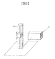
- FIG. 2 it can be realized by a single actuator 30 that moves up and down and a control system 31 to which the above-described motion program is input.
- the actuator 30 may be connected to the circuit board holder 110 (FIG. 6) so that the movement of the actuator 30 is reflected.
- the control system 31 can use the actuator 30 to perform the same vertical movement as in the first and second embodiments, and can perform an asymmetrical movement of a large ascending acceleration and a small descending acceleration having the same effect as the present invention. You can also.
- the accelerations during the ascending movement and the descending movement may be determined in advance, and the position may be determined for each time of the circuit board by integrating twice in time.
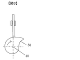
- FIG. 3 a mechanism that creates a vertical motion from a cam by attaching a cam 50 to a shaft 40 that performs a rotational motion, such as a motor, can also be realized.
- the acceleration in the ascending motion and the descending motion is determined in advance, and integration is performed twice in time, as described above.
- the cam can be produced by obtaining a cam curve from the determined position of the circuit board for each time. Also with the cam of the present embodiment, it is possible to perform an asymmetrical movement with a large ascending acceleration and a small descending acceleration.
Landscapes
- Engineering & Computer Science (AREA)
- Mechanical Engineering (AREA)
- Manufacturing & Machinery (AREA)
- Microelectronics & Electronic Packaging (AREA)
- Electric Connection Of Electric Components To Printed Circuits (AREA)
Abstract
本発明の目的は、鉛フリーはんだ使用時の、回路基板とはんだバンプ接続部品における、はんだバンプとはんだペーストの融合不良を、クランク機構やバイブレーションモータなど、基板を上下方向に正弦波振動させて慣性力を得る方法を使用する場合よりも減少させ、接続の信頼性を向上させることである。上記目的のために、回路基板を上下運動させながら、回路基板をリフロー接続するはんだ接続装置において、回路基板を載置する回路基板ホルダの上下運動を非対称とし、上昇運動は素早く、下降運動はゆっくり行うことのできる駆動機構を有するはんだ接続装置を提供する。
Description
本発明は、ボールグリッドアレイ等のはんだバンプ付き電子部品と回路基板とを、はんだによって接続する技術に関する。
電子部品と回路基板の接続には、はんだが広く用いられているが、従来このはんだには220℃付近ではんだ付けすることが出来るSn-37Pb(単位:質量%)が広く用いられてきた。しかし、鉛(Pb)は環境負荷が大きいので、鉛を用いないはんだの使用が求められている。鉛フリーはんだ合金は毒性が少ないが、一般的にぬれ性が悪い。本発明は、鉛フリーはんだを用いてボールグリッドアレイ(BGA(Ball Grid Array))等のはんだバンプ付き電子部品と回路基板とをリード線を用いずに接続する方法に関するものである。
また、鉛フリーはんだは、濡れ性が悪いほかに、溶融時の表面張力が従来のSn-37Pbはんだに比べて大きい。このため、リフローはんだ付け時に、ボールグリッドアレイのはんだバンプと、回路基板上に供給されたはんだペーストが溶融して液体になっても、その形状が変わりにくいことや、供給されたフラックスが各々の溶融はんだ間に存在することで、各々の溶融したはんだが融合するのには、大きな力が必要となっている。そして、このことが、はんだ接続部の未接続発生の主な原因となっている。
図1はボールグリッドアレイはんだバンプ付き電子部品と回路基板1を接続する様子を示す図である。図1(a)において、ボールグリッドアレイ10には円形などの部品電極11がマトリクス状に形成されており、さらにその上には、はんだバンプ12が形成されている。一方、回路基板1には、ボールグリッドアレイ10の部品電極11に対応して回路基板電極2がマトリクス状に形成されている。回路基板電極2には印刷等によってはんだペースト20が形成されている。以後、部品電極11のことをボールグリッドアレイ電極、回路基板電極2のことを基板ランドということもある。
図1(b)は、ボールグリッドアレイ10と回路基板1をはんだによって接続した状態を示すものであるが、この接続の際、以下の問題が発生する場合がある。
鉛フリーはんだでは、濡れ性が悪いほかに、溶融時の表面張力が従来のSn-37Pbはんだに比べて大きい。
このため、リフローはんだ付け時に、ボールグリッドアレイのはんだバンプと、回路基板上に供給されたはんだペーストが溶融して液体になっても、その形状が変わりにくいことや、供給されたフラックスが各々の溶融はんだ間に存在することで、各々の溶融したはんだが融合するのには、大きな力が必要となっており、この力が不足することで、はんだバンプとはんだペースの融合不良が生じる。
この力を補うためのアシスト力としては、回路基板を振動させ、部品に働く慣性力を得ることで、はんだの濡れ性を向上させ不良を低減させる方法がある(例えば、特許文献1参照)。
この場合、回路基板を振動させる手段としては、クランク機構やバイブレーションモータなど、基板を正弦波振動させて慣性力を得る方法が一般的である。
しかし、正弦波振動では、質量mの実装部品が受ける垂直抗力ベクトルは慣性力m・g‘と重力m・g(g:重力加速度)の和の逆方向ベクトル(向きが逆で大きさが等しい)となり、また垂直方向の慣性力の大きさがサインカーブ的な時間変化、
(数1) m・g‘ =m・g‘0・sin(2πft) (g‘0:一定値)
をするのが一般的である。そのため、部品は、
(数2) a=g‘0・sin(2πft)+g
の加速度で運動していることとなり、加速度が最大のときは、
(数3) g‘0+g
となり、部品が受ける垂直抗力が最大となる。
一方、最小のときは、
(数4) -g‘0+g
となり、部品が受ける垂直抗力も最小となるがこれが負の値になると部品は基板から離れてしまうためこれを避ける必要がある。
よって、未接続を防止する(部品が受ける垂直抗力を大きくする)ため、g’0を大きくするには限界があり、g‘0はg(g:重力加速度)以下にしなくてはいけないことから、加速度の最大値は
(数5) 2・g
となってしまう。
これは、一般的な機械的振動による慣性力では、部品が回路基板から受ける力は部品の重量の2倍以下となってしまうことを意味する。
(数1) m・g‘ =m・g‘0・sin(2πft) (g‘0:一定値)
をするのが一般的である。そのため、部品は、
(数2) a=g‘0・sin(2πft)+g
の加速度で運動していることとなり、加速度が最大のときは、
(数3) g‘0+g
となり、部品が受ける垂直抗力が最大となる。
一方、最小のときは、
(数4) -g‘0+g
となり、部品が受ける垂直抗力も最小となるがこれが負の値になると部品は基板から離れてしまうためこれを避ける必要がある。
よって、未接続を防止する(部品が受ける垂直抗力を大きくする)ため、g’0を大きくするには限界があり、g‘0はg(g:重力加速度)以下にしなくてはいけないことから、加速度の最大値は
(数5) 2・g
となってしまう。
これは、一般的な機械的振動による慣性力では、部品が回路基板から受ける力は部品の重量の2倍以下となってしまうことを意味する。
本発明の課題は、回路基板を振動させ、部品に働く慣性力を得る方法において、部品の運動の加速度が最大のとき及び最小のときの部品が受ける垂直抗力をできるだけ大きくし、はんだの接続信頼性の向上を可能とすることである。
上記課題を解決するために、本願発明は、回路基板を上下運動させながら、回路基板をリフロー接続するはんだ接続装置において、回路基板を載置する回路基板ホルダの上下運動を非対称し、上昇運動は素早く、下降運動はゆっくり行うことを特徴とする。
本発明によれば、上昇運動でははんだを圧縮する大きな力がかかるとともに、下降運動でははんだをはなす方向の力が小さいため、はんだの濡れ性を向上させはんだ接続の信頼性を向上させることができる。
本発明を実現する方法としては、回路基板に上下運動(上下とは鉛直方向を意味する)を与えながら回路基板をリフロー接続する装置において、この回路基板の上昇運動と下降運動がそれぞれ非対称となる機構が備わっている必要がある。そのとき、回路基板が上昇するときに上方向への加速度を大きく、回路基板が下降するときは下方向への加速度を小さくさせるような機構とする。
以下、実施例にて詳述する。
高価な機構や複雑な形状の部品を使用せず、回路基板に上下運動を与えるには、モータに取り付けた円盤などの一点の等速円周運動から上下方向の一軸方向の運動を取り出し、これを回路基板に与える方法としては、従来のクランク機構では上下対称運動となるため、これを改良することにより上下非対称運動を得ることを考える。
図4のような機構を作製し、この機構のモータなどにより軸40を中心に回転運動する円盤60の外側に支点61を設け、支点61から円盤60上の一点62の等速円周運動を眺めることとする。
また、大きな加速度が得られる可能性のある、速度の符号が反転するところを含むように、A点,B点を境界とし、円盤60上の一点62がA点からB点に動く場合(図4(a))と、B点からA点に動く場合(図4(b))とに分割して考える。
こうすると、支点61から見た円盤の一点62の運動は、図4(a)の運動と図4(b)の運動は、対称的な運動となってしまう。
こうすると、支点61から見た円盤の一点62の運動は、図4(a)の運動と図4(b)の運動は、対称的な運動となってしまう。
さらに、図5のように、この機構のモータなどの軸40と支点61を結ぶ線を水平とし、垂直(上下)運動できる第一のリニアガイド71を設け、円盤と支点を結ぶ真っ直ぐな第二のリニアガイド72とこの第一のリニアガイドの交点73の運動を取り出せるような機構を作製する。
なお、第一のリニアガイド71は、アウター部が不動部に固定されている。
また、第二のリニアガイド72には2個のアウター部が存在し、その内支点から遠い方のアウター部は円盤の一点62にあるピボットを介して円盤と結合され、支点に近い方のアウター部は第一のリニアガイド71のインナー部とピボットを介して結合されている。
さらに、第二のリニアガイド72のインナー部は、ピボットを介して不動部に固定されている。
さらに、回路基板ホルダは、第一のリニアガイド71のインナー部の頂点に結合されており、回路基板は、リフロー接続時には、回路基板ホルダに取り付けられる。
いま、図4(a)の運動と(b)の運動は、対称的な運動となっているので、図5の垂直(上下)運動も対称的となる。従って、上方向、下方向への加速度は共に等しくなってしまう。
そこで、上方向、下方向への加速度が等しくなることを避けるために、この機構のモータなどの軸40と支点61を結ぶ線と、第一のリニアガイド71が直交しないようにすることを考える。
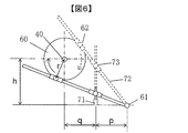
図6は、前述した機構を有する一つの例であり、円盤のついたモータなどの軸40と支点61の高さに距離hの差を与え、第一のリニアガイド71は、そのアウター部が機構底面に結合されており、この第一のリニアガイド71は機構に垂直に取り付けられた状態としている。
こうすれば、この機構は、モーターと円盤以外に、リニアガイドとピボットを組合わせるだけで組み立てることが可能なため、高価なプロセスを使用せず、かつ、精度の高い加工を必要とせずに回路基板に非対称な上下運動を与えながらリフロー接続が可能となるため、これを最良の方法として提案する。
図7は、この機構を回路基板のはんだ付け時に使用するため、この機構をリフロー炉100に組み込んだときの概略図である。
回路基板ホルダ110は、第一のリニアガイド71のインナー部の頂点に結合されておりリフロー炉チャンバー101内に存在し、回路基板1は、回路基板ホルダ110に取り付けられている。
回路基板ホルダ110は、第一のリニアガイド71のインナー部の頂点に結合されておりリフロー炉チャンバー101内に存在し、回路基板1は、回路基板ホルダ110に取り付けられている。
この機構を組み込んだリフロー炉100を使用すれば、回路基板の垂直(z)方向変位は計算によると以下の式のようになる。
z(t)={-p(h/r+sin(2πft))}/{(p+q)/r-cos(2πft)}
ただし、各記号は以下の数値である。
z:回路基板の垂直方向変位
t:時間
p:支点と、垂直に配置した第一のリニアガイド間の水平距離
q:垂直に配置した第一のリニアガイドと、回転円盤の中心間の水平距離
h:支点と回転円盤の中心間の高さの差(垂直距離)
r:回転円盤の半径
f:回転円盤の回転数
また、これを時間で二階微分したものと、g(g:重力加速度)を加えれば、回路基板に搭載された部品の垂直(z)方向の加速度が算出できるが、この値が2・gを超えることが可能となる。
ただし、各記号は以下の数値である。
z:回路基板の垂直方向変位
t:時間
p:支点と、垂直に配置した第一のリニアガイド間の水平距離
q:垂直に配置した第一のリニアガイドと、回転円盤の中心間の水平距離
h:支点と回転円盤の中心間の高さの差(垂直距離)
r:回転円盤の半径
f:回転円盤の回転数
また、これを時間で二階微分したものと、g(g:重力加速度)を加えれば、回路基板に搭載された部品の垂直(z)方向の加速度が算出できるが、この値が2・gを超えることが可能となる。
これにより、一般的な機械的振動を使用する場合と比較して、部品が基板から受ける力を大きく(部品の重力の2倍以上と)することができる。
このことにより、クランク機構やバイブレーションモータなど、回路基板を正弦波振動させて慣性力を得る方法を使用するよりも、はんだ未接続発生率の低下により貢献できるはんだ付けが可能となる。
本発明により、鉛フリーはんだを用いてボールグリッドアレイ(BGA(Ball Grid Array))等のはんだバンプ付き電子部品と回路基板とをリード線を用いずに接続する場合において、ボールグリッドアレイのはんだバンプと、回路基板上に供給されたはんだペーストが溶融して液体になった際の、各々の溶融したはんだが融合不良が原因となって起きる、はんだ接続部の未接続を、一般的な機械的振動を使用する場合と比較して、部品が基板から受けるアシスト力を大きく(部品に働く重力の2倍以上と)することができ、未接続発生率の低下に貢献できるはんだ付けが可能となる。
本発明により、鉛フリーはんだを用いてボールグリッドアレイ(BGA(Ball Grid Array))等のはんだバンプ付き電子部品と回路基板とをリード線を用いずに接続する場合において、ボールグリッドアレイのはんだバンプと、回路基板上に供給されたはんだペーストが溶融して液体になった際の、各々の溶融したはんだが融合不良が原因となって起きる、はんだ接続部の未接続を、一般的な機械的振動を使用する場合と比較して、部品が基板から受けるアシスト力を大きく(部品に働く重力の2倍以上と)することができ、未接続発生率の低下に貢献できるはんだ付けが可能となる。
本実施例では、図6の機構を組み込んだ図7のリフロー炉を用いて、汎用的な鉛フリーはんだであるSn-3Ag-0.5Cu(単位:質量%)はんだによるはんだバンプを持つボールグリッドアレイを、Sn-3Ag-0.5Cu(単位:質量%)はんだペーストにより回路基板に接続した。
なお、接続に使用したボールグリッドアレイは、
パッケージサイズ:42mm
バンプサイズ:0.76mm
バンプピッチ:1.27mm
バンプ数:784個(28×28)
である。
パッケージサイズ:42mm
バンプサイズ:0.76mm
バンプピッチ:1.27mm
バンプ数:784個(28×28)
である。
また、回路基板を上下運動させる機構部における、各寸法や回転数、
p:支点と、垂直に配置した第一のリニアガイド間の水平距離
q:垂直に配置した第一のリニアガイドと、回転円盤の中心間の水平距離
h:支点と回転円盤の中心間の高さの差(垂直距離)
r:回転円盤の半径
f:回転円盤の回転数
は、以下となっている。
p=2mm
q=12mm
h=63mm
r=7mm
f=5rps
上記の例では、部品に働く慣性力と重力の合力の影響で部品が基板から垂直上向きに受ける加速度の最大値は、重力加速度の2.84倍、垂直上向きに受ける加速度の最小値は重力加速度の0.41倍とできることがわかった。これを図8に示す。図8では、縦軸が1が重力加速度によるものであり、ここからの差分は回路基板の加速度によるものである。本実施例では、上昇するときの加速度は下降するときの加速度よりも大きくなっている。さらに、上昇するときの最大加速度も下降するときの最大加速度よりも大きく、上昇するときの平均加速度も下降するときの平均加速度よりも大きい。これは、上昇する時間が下降する時間より短くなっているためであり、短時間で素早く上昇し、長時間でゆっくりと下降することを表している。
p:支点と、垂直に配置した第一のリニアガイド間の水平距離
q:垂直に配置した第一のリニアガイドと、回転円盤の中心間の水平距離
h:支点と回転円盤の中心間の高さの差(垂直距離)
r:回転円盤の半径
f:回転円盤の回転数
は、以下となっている。
p=2mm
q=12mm
h=63mm
r=7mm
f=5rps
上記の例では、部品に働く慣性力と重力の合力の影響で部品が基板から垂直上向きに受ける加速度の最大値は、重力加速度の2.84倍、垂直上向きに受ける加速度の最小値は重力加速度の0.41倍とできることがわかった。これを図8に示す。図8では、縦軸が1が重力加速度によるものであり、ここからの差分は回路基板の加速度によるものである。本実施例では、上昇するときの加速度は下降するときの加速度よりも大きくなっている。さらに、上昇するときの最大加速度も下降するときの最大加速度よりも大きく、上昇するときの平均加速度も下降するときの平均加速度よりも大きい。これは、上昇する時間が下降する時間より短くなっているためであり、短時間で素早く上昇し、長時間でゆっくりと下降することを表している。
また、比較のために、上下対称運動となる図9のようなクランク機構を使用し、これに回路基板に前述の方式と振動数や振幅が同じになるように、上下運動を与えながらリフロー接続を実施した。
その結果、部品に働く慣性力と重力の合力の影響で部品が基板から垂直上向きに受ける加速度の最大値は、重力加速度の1.62倍、垂直上向きに受ける加速度の最小値は重力加速度の0.38倍とできることがわかった。これを図10に示す。
これらのリフロー炉を使用して、
プリヒート温度:160℃
プリヒート時間:90秒
ピーク温度:235℃
220℃超過時間:40秒
の温度プロファイルでリフロー接続を行った。
プリヒート温度:160℃
プリヒート時間:90秒
ピーク温度:235℃
220℃超過時間:40秒
の温度プロファイルでリフロー接続を行った。
その結果、図7の本案のリフロー炉では、BGA100個中、接続不良が発生したものは、0個であった。
しかし、図9のクランク機構を使用したリフロー炉では、BGA100個中、接続不良が発生したものは、5個であった。
上記の結果より、本実施例によるリフロー炉により、BGAの接続不良率は大きく改善されていることが確認できた。
本実施例では、図6の機構を組み込んだ図7のリフロー炉を用いて、汎用的な鉛フリーはんだであるSn-3Ag-0.5Cu(単位:質量%)はんだによるはんだバンプを持つチップサイズパッケージ(CSP(Chip Size Package))を、Sn-3Ag-0.5Cu(単位:質量%)はんだペーストにより回路基板に接続した。
なお、接続に使用したチップサイズパッケージは、
パッケージサイズ:19mm
バンプサイズ:0.5mm
バンプピッチ:0.8mm
バンプ数:484個
であり、この部品は、BGAと比較すると部品の質量が小さいため、1Gの重力下では部品の重力が部品を回路基板に押し付ける力が小さくなっている。
パッケージサイズ:19mm
バンプサイズ:0.5mm
バンプピッチ:0.8mm
バンプ数:484個
であり、この部品は、BGAと比較すると部品の質量が小さいため、1Gの重力下では部品の重力が部品を回路基板に押し付ける力が小さくなっている。
また、回路基板を上下運動させる機構部における、各寸法や回転数、
p:支点と、垂直に配置した第一のリニアガイド間の水平距離
q:垂直に配置した第一のリニアガイドと、回転円盤の中心間の水平距離
h:支点と回転円盤の中心間の高さの差(垂直距離)
r:回転円盤の半径
f:回転円盤の回転数
は、以下となっている。
p=2mm
q=12mm
h=63mm
r=4.5mm
f=10rps
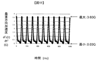
上記の例では、部品に働く慣性力と重力の合力の影響で部品が基板から垂直上向きに受ける加速度の最大値は、重力加速度の3.60倍、垂直上向きに受ける加速度の最小値は重力加速度の0.03倍とできることがわかった。これを図11に示す。
p:支点と、垂直に配置した第一のリニアガイド間の水平距離
q:垂直に配置した第一のリニアガイドと、回転円盤の中心間の水平距離
h:支点と回転円盤の中心間の高さの差(垂直距離)
r:回転円盤の半径
f:回転円盤の回転数
は、以下となっている。
p=2mm
q=12mm
h=63mm
r=4.5mm
f=10rps
上記の例では、部品に働く慣性力と重力の合力の影響で部品が基板から垂直上向きに受ける加速度の最大値は、重力加速度の3.60倍、垂直上向きに受ける加速度の最小値は重力加速度の0.03倍とできることがわかった。これを図11に示す。
また、比較のために、上下対称運動となる図9のようなクランク機構を使用し、これに回路基板に前述の方式と振動数や振幅が同じになるように、上下運動を与えながらリフロー接続を検討した。
その結果、部品に働く慣性力と重力の合力の影響で部品が基板から垂直上向きに受ける加速度の最大値は、重力加速度の2.34倍となるが、部品が基板から垂直上向きに受ける加速度は0より小さくなり、部品に力が全く働かなくなることにより浮遊してしまうことがわかったため、クランク機構の実験は断念した。
そこで、図7のリフロー炉における上下動機構のスイッチを入れた場合と、入れなかった場合の比較をすることにした。
なお、CSPは、
プリヒート温度:160℃
プリヒート時間:70秒
ピーク温度:235℃
220℃超過時間:35秒
の温度プロファイルでリフロー接続を行った。
プリヒート温度:160℃
プリヒート時間:70秒
ピーク温度:235℃
220℃超過時間:35秒
の温度プロファイルでリフロー接続を行った。
その結果、図7のリフロー炉における上下動機構のスイッチを入れた場合では、CSP100個中、接続不良が発生したものは、0個であった。
しかし、リフロー炉における上下動機構のスイッチを入れなかった場合では、CSP100個中、接続不良が発生したものは、4個であった。
上記の結果より、BGAと比較すると部品の質量が小さいため、1Gの重力下では部品の重力が部品を回路基板に押し付ける力が小さいCSPに対しても、本実施例によるリフロー炉により、接続不良率は大きく改善されていることが確認できた。
本発明の他の実施例を説明する。本実施例では、図2のように、上下運動する一本のアクチュエータ30と前述の運動プログラムがインプットされた制御系31とで実現することができる。アクチュエータ30を回路基板ホルダ110(図6)に接続し、アクチュエータ30の動きが反映されるようにすればよい。制御系31は、アクチュエータ30を用いて、実施例1,2と同様の上下運動を行うこともできるし、本発明と効果を有する、大きな上昇加速度と小さな下降加速度の上下非対称の運動を行うこともできる。
なお、運動プログラムは上昇運動時と下降運動時の各々の加速度を先に決めておき、時間で2回の積分をすることにより、決定した回路基板の各時間ごとの位置とすれば良い。
さらに、他の実施例を説明する。図3のように、モータなどの回転運動をする軸40にカム50を取り付け、カムから上下運動を作り出す機構でも、実現することができる。
この機構には、回路基板に目的の上下運動をさせるために、上記と同様に、上昇運動時と下降運動時の各々の加速度を先に決めておき、時間で2回の積分をすることにより、決定した回路基板の各時間ごとの位置からカム曲線を求めてカムを作製すれば良いことになる。本実施例のカムによっても、大きな上昇加速度と小さな下降加速度の上下非対称の運動を行うことができる。
1・・・回路基板
2・・・回路基板ランド(回路基板電極)
10・・・ボールグリッドアレイ
11・・・部品電極
12・・・はんだバンプ
20・・・はんだペースト
30・・・上下運動アクチュエータ
31・・・制御系
40・・・モータなどの軸
50・・・カム
60・・・回転運動する円盤
61・・・支点
62・・・円盤上の一点
71・・・垂直(上下)運動できる第一のリニアガイド
72・・・第二のリニアガイド
100・・・リフロー炉
101・・・リフロー炉チャンバー
110・・・回路基板ホルダ
2・・・回路基板ランド(回路基板電極)
10・・・ボールグリッドアレイ
11・・・部品電極
12・・・はんだバンプ
20・・・はんだペースト
30・・・上下運動アクチュエータ
31・・・制御系
40・・・モータなどの軸
50・・・カム
60・・・回転運動する円盤
61・・・支点
62・・・円盤上の一点
71・・・垂直(上下)運動できる第一のリニアガイド
72・・・第二のリニアガイド
100・・・リフロー炉
101・・・リフロー炉チャンバー
110・・・回路基板ホルダ
Claims (9)
- 回路基板を保持する回路基板ホルダと、
前記回路基板を加熱する加熱手段と、
前記回路基板ホルダに上下運動を与える駆動手段とを備え、
回路基板に上下運動を与えながら回路基板をリフロー接続するはんだ接続装置において、
前記駆動手段は、前記回路基板ホルダを、上昇するときの加速度が下降するときの加速度よりも大きくなるように上下運動させることを特徴とするはんだ接続装置。 - 請求項1において、
前記駆動手段は、前記回路基板ホルダを、上昇するときの最大加速度が下降するときの最大加速度よりも大きくなるように上下運動させることを特徴とするはんだ接続装置。 - 請求項1または請求項2において、
前記駆動手段は、前記回路基板ホルダを、上昇するときの平均加速度が下降するときの平均加速度よりも大きくなるように上下運動させることを特徴とするはんだ接続装置。 - 請求項1乃至3のいずれかにおいて、
前記駆動手段は、前記回路基板ホルダを、上昇する時間が下降する時間よりも短くなるように上下運動させることを特徴とするはんだ接続装置。 - 請求項2において、
前記上昇するときの最大加速度の絶対値は、重力による加速度の絶対値よりも大きく、
前記下降するときの最大加速度の絶対値は、重力による加速度の絶対値よりも小さいことを特徴とするはんだ接続装置。 - 請求項1乃至5のいずれかにおいて、
前記駆動手段は、
回転軸を中心に回転する円盤と、
前記回転軸よりも下方にある第1の支点と、
前記支点と前記円盤上の第2の支点を通すように設けられた第1のロッドと、
前記支点と前記円盤上の一点との間で前記第1のロッドに、略鉛直方向に可動に接続され、前記回路基板ホルダに前記上下方向の運動を伝達する第2のロッドとを備えたことを特徴とするはんだ接続装置。 - 請求項1乃至5のいずれかにおいて、
前記駆動手段は、上下運動をする一本のアクチュエータと、当該アクチュエータを制御する制御手段とを有することを特徴とする請求項1に記載の装置。 - 請求項1乃至5のいずれかにおいて、
前記駆動手段は、カムと、当該カムにより上下運動するロッドとを有することを特徴とする請求項1に記載の装置。 - 回路基板を上下運動させながら加熱してリフロー接続を行うはんだ接続方法において、
前記回路基板の上下運動は、上昇するときの加速度が下降するときの加速度よりも大きいことを特徴とするはんだ接続方法。
Applications Claiming Priority (2)
| Application Number | Priority Date | Filing Date | Title |
|---|---|---|---|
| JP2010-242966 | 2010-10-29 | ||
| JP2010242966A JP2012094789A (ja) | 2010-10-29 | 2010-10-29 | はんだ接続装置及び方法 |
Publications (1)
| Publication Number | Publication Date |
|---|---|
| WO2012056667A1 true WO2012056667A1 (ja) | 2012-05-03 |
Family
ID=45993415
Family Applications (1)
| Application Number | Title | Priority Date | Filing Date |
|---|---|---|---|
| PCT/JP2011/005918 Ceased WO2012056667A1 (ja) | 2010-10-29 | 2011-10-24 | はんだ接続装置及び方法 |
Country Status (2)
| Country | Link |
|---|---|
| JP (1) | JP2012094789A (ja) |
| WO (1) | WO2012056667A1 (ja) |
Citations (3)
| Publication number | Priority date | Publication date | Assignee | Title |
|---|---|---|---|---|
| JPH08330722A (ja) * | 1995-05-30 | 1996-12-13 | Nec Corp | 電子部品のはんだ付け方法 |
| JP2007281272A (ja) * | 2006-04-10 | 2007-10-25 | Matsushita Electric Ind Co Ltd | リフロー装置及び方法 |
| JP2009094370A (ja) * | 2007-10-11 | 2009-04-30 | Hitachi Ltd | はんだ付け方法及びリフローはんだ付け装置 |
-
2010
- 2010-10-29 JP JP2010242966A patent/JP2012094789A/ja active Pending
-
2011
- 2011-10-24 WO PCT/JP2011/005918 patent/WO2012056667A1/ja not_active Ceased
Patent Citations (3)
| Publication number | Priority date | Publication date | Assignee | Title |
|---|---|---|---|---|
| JPH08330722A (ja) * | 1995-05-30 | 1996-12-13 | Nec Corp | 電子部品のはんだ付け方法 |
| JP2007281272A (ja) * | 2006-04-10 | 2007-10-25 | Matsushita Electric Ind Co Ltd | リフロー装置及び方法 |
| JP2009094370A (ja) * | 2007-10-11 | 2009-04-30 | Hitachi Ltd | はんだ付け方法及びリフローはんだ付け装置 |
Also Published As
| Publication number | Publication date |
|---|---|
| JP2012094789A (ja) | 2012-05-17 |
Similar Documents
| Publication | Publication Date | Title |
|---|---|---|
| JP5160450B2 (ja) | 回路基板上への半導体部品の搭載方法 | |
| JP4938980B2 (ja) | 非共晶はんだ組成物 | |
| CN103295991B (zh) | 用于使半导体组合件中的焊料凸块自对准的双焊料半导体芯片、装置以及双焊料方法 | |
| US9978709B2 (en) | Solder bump stretching method for forming a solder bump joint in a device | |
| JP6365841B2 (ja) | 実装構造体とその製造方法 | |
| JP5097038B2 (ja) | はんだ付け方法及びはんだ付け装置 | |
| JP2009224471A (ja) | 電子部品及びその製造方法 | |
| JP2011171427A (ja) | 積層型半導体装置 | |
| WO2012056667A1 (ja) | はんだ接続装置及び方法 | |
| JP5607694B2 (ja) | 自重を用いる半田ボール実装装置、これを含む半田ボール実装システム、及びこれを用いる半田ボール実装方法 | |
| JP6124032B2 (ja) | 実装構造体と実装構造体の製造方法 | |
| JP5004549B2 (ja) | 電子部品の基板への搭載方法及びはんだ面の形成方法 | |
| JP5226937B2 (ja) | フリップチップボンディング技術を用いた、半導体チップの基板への実装方法 | |
| CN202555931U (zh) | 一种激光软钎焊中激光头升降与焊锡丝旋转的装置 | |
| JP4696110B2 (ja) | 電子部品の実装方法及び電子部品実装装置 | |
| JP4283091B2 (ja) | 電子部品の実装方法 | |
| JP4260712B2 (ja) | 電子部品実装方法及び装置 | |
| US20130221074A1 (en) | Solder bump stretching method | |
| JP4940662B2 (ja) | はんだバンプ、はんだバンプの形成方法及び半導体装置 | |
| CN118893261A (zh) | 一种用于cga器件封装的摩擦钎焊方法 | |
| JP2011198777A (ja) | はんだ接合方法及びはんだ継手 | |
| JP2007048987A (ja) | フリップチップ実装方法 | |
| JP4606376B2 (ja) | 半導体装置 | |
| JP2010206166A (ja) | 回路基板構造体 | |
| CN1929950A (zh) | 包括抗疲劳三元焊接合金的半导体装置的组装方法 |
Legal Events
| Date | Code | Title | Description |
|---|---|---|---|
| 121 | Ep: the epo has been informed by wipo that ep was designated in this application |
Ref document number: 11835814 Country of ref document: EP Kind code of ref document: A1 |
|
| NENP | Non-entry into the national phase |
Ref country code: DE |
|
| 122 | Ep: pct application non-entry in european phase |
Ref document number: 11835814 Country of ref document: EP Kind code of ref document: A1 |