WO2012053161A1 - 薄膜トランジスタ基板の製造方法およびその方法により製造された薄膜トランジスタ基板 - Google Patents
薄膜トランジスタ基板の製造方法およびその方法により製造された薄膜トランジスタ基板 Download PDFInfo
- Publication number
- WO2012053161A1 WO2012053161A1 PCT/JP2011/005681 JP2011005681W WO2012053161A1 WO 2012053161 A1 WO2012053161 A1 WO 2012053161A1 JP 2011005681 W JP2011005681 W JP 2011005681W WO 2012053161 A1 WO2012053161 A1 WO 2012053161A1
- Authority
- WO
- WIPO (PCT)
- Prior art keywords
- semiconductor layer
- film
- oxide semiconductor
- forming
- insulating film
- Prior art date
- Legal status (The legal status is an assumption and is not a legal conclusion. Google has not performed a legal analysis and makes no representation as to the accuracy of the status listed.)
- Ceased
Links
Images



Classifications
-
- H—ELECTRICITY
- H10—SEMICONDUCTOR DEVICES; ELECTRIC SOLID-STATE DEVICES NOT OTHERWISE PROVIDED FOR
- H10D—INORGANIC ELECTRIC SEMICONDUCTOR DEVICES
- H10D30/00—Field-effect transistors [FET]
- H10D30/01—Manufacture or treatment
- H10D30/021—Manufacture or treatment of FETs having insulated gates [IGFET]
- H10D30/031—Manufacture or treatment of FETs having insulated gates [IGFET] of thin-film transistors [TFT]
-
- H—ELECTRICITY
- H10—SEMICONDUCTOR DEVICES; ELECTRIC SOLID-STATE DEVICES NOT OTHERWISE PROVIDED FOR
- H10D—INORGANIC ELECTRIC SEMICONDUCTOR DEVICES
- H10D30/00—Field-effect transistors [FET]
- H10D30/60—Insulated-gate field-effect transistors [IGFET]
- H10D30/67—Thin-film transistors [TFT]
- H10D30/6704—Thin-film transistors [TFT] having supplementary regions or layers in the thin films or in the insulated bulk substrates for controlling properties of the device
-
- H—ELECTRICITY
- H10—SEMICONDUCTOR DEVICES; ELECTRIC SOLID-STATE DEVICES NOT OTHERWISE PROVIDED FOR
- H10D—INORGANIC ELECTRIC SEMICONDUCTOR DEVICES
- H10D30/00—Field-effect transistors [FET]
- H10D30/60—Insulated-gate field-effect transistors [IGFET]
- H10D30/67—Thin-film transistors [TFT]
- H10D30/674—Thin-film transistors [TFT] characterised by the active materials
- H10D30/6755—Oxide semiconductors, e.g. zinc oxide, copper aluminium oxide or cadmium stannate
-
- H—ELECTRICITY
- H10—SEMICONDUCTOR DEVICES; ELECTRIC SOLID-STATE DEVICES NOT OTHERWISE PROVIDED FOR
- H10D—INORGANIC ELECTRIC SEMICONDUCTOR DEVICES
- H10D30/00—Field-effect transistors [FET]
- H10D30/60—Insulated-gate field-effect transistors [IGFET]
- H10D30/67—Thin-film transistors [TFT]
- H10D30/674—Thin-film transistors [TFT] characterised by the active materials
- H10D30/6755—Oxide semiconductors, e.g. zinc oxide, copper aluminium oxide or cadmium stannate
- H10D30/6756—Amorphous oxide semiconductors
-
- H—ELECTRICITY
- H10—SEMICONDUCTOR DEVICES; ELECTRIC SOLID-STATE DEVICES NOT OTHERWISE PROVIDED FOR
- H10D—INORGANIC ELECTRIC SEMICONDUCTOR DEVICES
- H10D99/00—Subject matter not provided for in other groups of this subclass
-
- H—ELECTRICITY
- H10—SEMICONDUCTOR DEVICES; ELECTRIC SOLID-STATE DEVICES NOT OTHERWISE PROVIDED FOR
- H10D—INORGANIC ELECTRIC SEMICONDUCTOR DEVICES
- H10D30/00—Field-effect transistors [FET]
- H10D30/01—Manufacture or treatment
- H10D30/021—Manufacture or treatment of FETs having insulated gates [IGFET]
- H10D30/031—Manufacture or treatment of FETs having insulated gates [IGFET] of thin-film transistors [TFT]
- H10D30/0312—Manufacture or treatment of FETs having insulated gates [IGFET] of thin-film transistors [TFT] characterised by the gate electrodes
Definitions
- the present invention relates to a method of manufacturing a thin film transistor substrate, and more particularly to a method of manufacturing a thin film transistor substrate using a semiconductor layer of an oxide semiconductor and a thin film transistor substrate manufactured by the method.
- a thin film transistor (hereinafter also referred to as “TFT”) is provided as a switching element for each pixel which is the minimum unit of an image.
- a typical bottom gate type TFT has, for example, a gate electrode provided on an insulating substrate, a gate insulating film provided so as to cover the gate electrode, and an island shape so as to overlap the gate electrode on the gate insulating film. And a source electrode and a drain electrode provided to face each other on the semiconductor layer.
- an IGZO In-Ga-Zn-O
- a conventional thin film transistor that uses an amorphous silicon semiconductor layer as a switching element of each pixel that is the minimum unit of an image.
- a TFT using an oxide semiconductor layer hereinafter also referred to as an “oxide semiconductor layer” formed of an oxide semiconductor film is proposed.
- an insulating layer a gate electrode provided over the insulating layer, an oxide semiconductor layer provided over the gate electrode through a gate insulating film, and a gate over the oxide semiconductor layer
- the source electrode and the drain electrode that are provided so as to sandwich the electrode, and the oxide that is provided between the source electrode, the drain electrode, and the oxide semiconductor layer and is exposed from the source electrode and the drain electrode on the gate electrode
- a thin film transistor substrate including a channel protective film covering at least a part of a side surface of a semiconductor layer is disclosed.
- a step of forming a gate electrode on the substrate, a step of forming a gate insulating film on the gate electrode, and an oxide semiconductor layer on the gate insulating film are formed.
- a step and a step of forming a channel protective film so as to cover at least part of the side surface of the oxide semiconductor layer over the gate electrode are performed.
- the oxide semiconductor layer and the channel protective film are heat-treated at a temperature of 160 ° C. or higher, and then a source electrode and a drain electrode are formed over the oxide semiconductor layer and the channel protective film, and five sheets are formed.
- the photomask is used to manufacture a thin film transistor substrate (see, for example, Patent Document 1).
- the present invention has been made in view of the above-described problems, and provides a thin film transistor substrate manufacturing method capable of manufacturing a thin film transistor substrate with a smaller number of masks than before and a thin film transistor substrate manufactured by the method. With the goal.
- a first thin film transistor substrate manufacturing method of the present invention includes an insulating substrate, a gate electrode provided on the insulating substrate, a gate insulating film provided to cover the gate electrode, and gate insulation.
- a thin film transistor including an oxide semiconductor layer provided over a film and having a channel region, a source electrode provided over the oxide semiconductor layer so as to overlap with a gate electrode, and a channel protective film provided so as to cover the channel region
- a thin film transistor substrate comprising: an interlayer insulating film provided to cover the thin film transistor; and a planarizing film provided to cover the interlayer insulating film, wherein the insulating film is insulated using a first photomask.
- a gate electrode forming step for forming a gate electrode on the substrate, and a gate insulation for forming a gate insulating film on the insulating substrate so as to cover the gate electrode Forming a channel, forming a semiconductor layer on the gate insulating film, forming a semiconductor layer, and forming a channel protective film on the oxide semiconductor layer so as to cover the channel region using the second photomask
- a source electrode formation step for forming a source electrode on the oxide semiconductor layer, and an oxide semiconductor layer, a channel protection film, and an interlayer insulating film that covers the source electrode are formed using a third photomask
- a channel protective film removing step of removing the Mamorumaku characterized in that at least and a plasma treatment step for performing a plasma treatment on the oxide semiconductor layer at the opening.
- the thin film transistor can be manufactured with a smaller number of masks (4) than the prior art, the manufacturing cost can be reduced and the yield can be effectively suppressed.
- a thin film transistor substrate can be manufactured with a smaller number of masks (four) than the conventional technique without causing the disadvantage that it is difficult to form a fine pattern. .
- the second thin film transistor substrate manufacturing method of the present invention includes an insulating substrate, a gate electrode provided on the insulating substrate, a gate insulating film provided to cover the gate electrode, a gate insulating film provided on the gate insulating film, and a channel region.
- a thin film transistor including a source electrode provided on the oxide semiconductor layer so as to overlap with the gate electrode, a channel protective film provided so as to cover the channel region, and a thin film transistor provided so as to cover the thin film transistor A method of manufacturing a thin film transistor substrate including the interlayer insulating film, wherein the gate electrode is formed on the insulating substrate using the first photomask, and the gate electrode is covered on the insulating substrate.
- Gate insulating film forming step for forming a gate insulating film and a semiconductor layer forming process for forming an oxide semiconductor layer on the gate insulating film A channel protective film forming step of forming a channel protective film so as to cover the channel region on the oxide semiconductor layer using the second photomask; and a source on the oxide semiconductor layer using the third photomask.
- the thin film transistor can be manufactured with a smaller number of masks (4) than the prior art, the manufacturing cost can be reduced and the yield can be effectively suppressed.
- a thin film transistor substrate can be manufactured with a smaller number of masks (four) than the conventional technique without causing the disadvantage that it is difficult to form a fine pattern. .
- a reducing plasma treatment may be performed as the plasma treatment.
- a drain electrode or a pixel electrode can be formed by plasma treatment of the oxide semiconductor layer by a simple method without using a separate mask.
- indium (In), gallium (Ga), aluminum (Al), copper (Cu) is used as the oxide semiconductor material for forming the oxide semiconductor layer.
- the oxide semiconductor layer made of these materials has high mobility even if it is amorphous, so that the on-resistance of the switching element can be increased.
- indium gallium zinc oxide may be used as the oxide semiconductor material.
- the thin film transistor substrate of the present invention is a thin film transistor substrate manufactured by the first or second thin film transistor substrate manufacturing method of the present invention.
- the present invention it is possible to provide a thin film transistor substrate capable of reducing the manufacturing cost and effectively suppressing the yield reduction.
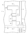
- FIG. 1 is a plan view of a thin film transistor substrate according to an embodiment of the present invention. It is the top view to which the pixel part of the thin-film transistor substrate which concerns on embodiment of this invention was expanded.
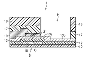
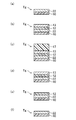
- FIG. 3 is a cross-sectional view of the thin film transistor substrate according to the embodiment of the present invention, and is a cross-sectional view taken along the line AA of FIG. 2 is a cross-sectional view of a terminal (gate terminal) of the thin film transistor substrate according to the embodiment of the present invention, and is a cross-sectional view taken along the line BB of FIG. It is explanatory drawing which shows the manufacturing process of the thin-film transistor substrate which concerns on embodiment of this invention in a cross section.
- FIG. 1 is a plan view of a thin film transistor substrate according to an embodiment of the present invention
- FIG. 2 is an enlarged plan view of a pixel portion of the thin film transistor substrate according to an embodiment of the present invention.
- FIG. 3 is a cross-sectional view of the thin film transistor substrate according to the embodiment of the present invention, and is a cross-sectional view taken along the line AA of FIG. 4 is a cross-sectional view of a terminal (gate terminal) of the thin film transistor substrate according to the embodiment of the present invention, and is a cross-sectional view taken along the line BB of FIG.
- the thin film transistor substrate 1 includes a display area D for displaying an image and a drive circuit area T provided around the display area D.
- a gate driver region Tg and a source driver region Ts are provided in the drive circuit region T.
- the gate driver region Tg is provided with a gate driver (not shown) for driving the gate wiring (scanning wiring) 11 in the display region D
- the source driver region Ts has a source wiring (signal) in the display region D.
- a source driver (not shown) for driving the wiring 16 is provided.
- the gate wiring 11 is drawn out to the gate driver region Tg of the drive circuit region T, and is connected to the gate terminal 22 in the gate driver region Tg.
- the gate terminal 22 is formed on the insulating substrate 10 in the gate driver region Tg.
- the source wiring 16 is led out as a relay wiring to the source driver area Ts of the driving circuit area T, and is connected to the source terminal 20 in the source driver area Ts.
- the source terminal 20 is formed on the insulating substrate 10 in the source driver region Ts.
- the thin film transistor substrate 1 includes an insulating substrate 10 and a plurality of gate wirings 11 provided so as to extend in parallel with each other on the insulating substrate 10 in the display region D where image display is performed.
- a plurality of source wirings 16 are provided on the insulating substrate 10 so as to extend in parallel with each other.
- the thin film transistor substrate 1 includes a thin film transistor 5, an interlayer insulating film (protective film) 17 provided so as to cover the thin film transistor 5, and a planarization provided so as to cover the interlayer insulating film 17. And a film 18.
- the thin film transistor 5 includes a gate electrode 15 provided on the insulating substrate 10, a gate insulating film 12 provided so as to cover the gate electrode 15, and a gate on the gate insulating film 12. And an oxide semiconductor layer 13 having a channel region C provided in an island shape so as to overlap with the electrode 15.
- the thin film transistor 5 includes a channel protective film 21 provided so as to cover the channel region C of the oxide semiconductor layer 13 and a source electrode 19 provided on the oxide semiconductor layer 13 so as to overlap the gate electrode 15. I have.
- an opening H is formed in the laminated film of the interlayer insulating film 17 and the planarizing film 18. Then, plasma treatment is performed on the oxide semiconductor layer 13 in the opening H to reduce the resistance of a part of the oxide semiconductor layer 13, whereby a part of the oxide semiconductor layer 13 in the opening H is drain electrode.
- the oxide semiconductor layer 13 in the opening H functions as a pixel electrode 13b while functioning as the pixel electrode 13a. In the opening H, the drain electrode 13a is connected to the pixel electrode 13b.
- the drain electrode 13a and the source electrode 19 are provided so as to face each other with the channel region C of the oxide semiconductor layer 13 interposed therebetween, as shown in FIG.
- the source electrode 19 is a portion where the source wiring 16 protrudes to the side
- the gate electrode 15 is a portion where the gate wiring 11 protrudes to the side.
- a protective layer 25 made of the same material as that of the channel protective film 21 is provided at a portion where the gate wiring 11 and the source wiring 16 intersect. Yes.
- the oxide semiconductor layer 13, the drain electrode 13a, and the pixel electrode 13b are formed of an oxide semiconductor film made of, for example, indium gallium zinc oxide (IGZO).
- IGZO indium gallium zinc oxide
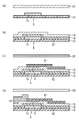
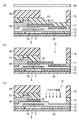
- FIG. 5 to 7 are explanatory views showing in cross section the manufacturing process of the thin film transistor substrate according to the embodiment of the present invention.
- a molybdenum film (thickness of about 150 nm) or the like is formed on the entire substrate of the insulating substrate 10 such as a glass substrate or a plastic substrate by a sputtering method. Thereafter, the molybdenum film is subjected to resist patterning by photolithography using the first photomask 31 having a predetermined pattern shape, wet etching, and resist peeling and cleaning, so that FIGS. As shown in FIG. 2A, the gate wiring 11 (see FIG. 2), the gate electrode 15 and the gate terminal 22 are formed on the insulating substrate 10.
- a single-layered molybdenum film is exemplified as the metal film constituting the gate wiring 11, the gate electrode 15, and the gate terminal 22.
- the metal film constituting the gate wiring 11, the gate electrode 15, and the gate terminal 22 may be formed to a thickness of 50 nm to 300 nm using a metal film such as a titanium film or a copper film, or a film of an alloy film or metal nitride thereof. good.
- polyethylene terephthalate resin polyethylene naphthalate resin
- polyether sulfone resin acrylic resin
- polyimide resin polyimide resin
- a silicon nitride film (thickness of about 200 nm to 500 nm) is formed by CVD on the entire substrate on which the gate wiring 11, the gate electrode 15, and the gate terminal 22 are formed, and FIG. As shown in FIG. 7B, the gate insulating film 12 is formed on the insulating substrate 10 so as to cover the gate wiring 11, the gate electrode 15, and the gate terminal 22.
- the gate insulating film 12 may have a two-layer structure.
- a silicon oxide film (SiOx), a silicon oxynitride film (SiOxNy, x> y), a silicon nitride oxide film (SiNxOy, x> y), or the like is used in addition to the above-described silicon nitride film (SiNx). be able to.
- a silicon nitride film or a silicon nitride oxide film is used as a lower gate insulating film, and a silicon oxide film as an upper gate insulating film, Alternatively, a structure using a silicon oxynitride film is preferable.
- a silicon nitride film having a thickness of 100 nm to 200 nm is formed as a lower gate insulating film using SiH 4 and NH 3 as reaction gases, and N 2 O and SiH 4 are reacted as an upper gate insulating film.
- a silicon oxide film with a thickness of 50 nm to 100 nm can be formed as a gas.
- a rare gas such as argon gas in the reaction gas and mix it in the insulating film.
- an oxide semiconductor film (thickness of about 30 nm to 100 nm) formed of, for example, indium gallium zinc oxide (IGZO) is formed by sputtering, as shown in FIGS. 5B and 7B. Then, the oxide semiconductor layer 13 is formed over the gate insulating film 12.
- IGZO indium gallium zinc oxide
- this embodiment is different from the above-described conventional technique in that resist patterning, wet etching, and resist peeling cleaning by photolithography using a photomask are not performed on the oxide semiconductor film.
- a silicon nitride film, a silicon oxide film, a silicon nitride oxide film, or the like is formed over the entire substrate over which the oxide semiconductor layer 13 is formed by a plasma CVD method. Thereafter, the silicon nitride film or the like is subjected to resist patterning by photolithography using the second photomask 32 having a predetermined pattern shape, wet etching, and resist peeling and cleaning, so that FIG. As shown, a channel protective film 21 for protecting the channel region C is formed on the oxide semiconductor layer 13 so as to cover the channel region C.
- a silicon oxide film having a thickness of 100 nm to 200 nm can be formed using SiH 4 and N 2 O as reaction gases.
- the protective layer 25 (see FIG. 2) described above is formed simultaneously with the formation of the channel protective film 21.
- a titanium film (thickness: 30 nm to 150 nm) and an aluminum film (thickness: about 50 nm to 400 nm) are sequentially formed on the entire substrate on which the oxide semiconductor layer 13 is formed by a sputtering method.
- the source electrode 19 composed of a laminated film of the first conductive layer made of a titanium film and the second conductive layer made of an aluminum film is formed on the oxide semiconductor layer 13. .
- a source wiring 16 and a source terminal 20 constituted by a laminated film of a first conductive layer made of a titanium film and a second conductive layer made of an aluminum film are formed. .
- etching process either dry etching or wet etching described above may be used. However, when processing a large area substrate, it is preferable to use dry etching.
- a fluorine-based gas such as CF 4 , NF 3 , SF 6 , or CHF 3
- a chlorine-based gas such as Cl 2 , BCl 3 , SiCl 4 , or CCl 4
- an oxygen gas or the like
- an inert gas such as argon may be added.
- a silicon nitride film, a silicon oxide film, a silicon nitride oxide film, or the like is formed on the entire substrate on which the source electrode 19 and the source wiring 16 are formed by a plasma CVD method.
- an interlayer insulating film 17 covering the oxide semiconductor layer 13, the channel protective film 21, the source electrode 19, and the source wiring 16 is formed to a thickness of about 250 nm.
- the interlayer insulating film 17 is not limited to a single layer structure, and may have a two-layer structure or a three-layer structure.
- the gate terminal 22 formed on the insulating substrate 10 is formed by forming the interlayer insulating film 17 in this step.
- a gate insulating film 12, an oxide semiconductor layer 13, and an interlayer insulating film 17 are sequentially stacked thereover.
- a photosensitive organic insulating film made of photosensitive acrylic resin or the like is formed to a thickness of about 1.0 ⁇ m to 3.0 ⁇ m on the entire substrate on which the interlayer insulating film 17 is formed by spin coating or slit coating. Apply.
- a planarizing film 18 having an opening corresponding to the opening H is formed on the surface of the interlayer insulating film 17.
- etching step> by using the planarizing film 18 as a mask, dry etching using a predetermined etching gas (for example, CF 4 gas and O 2 gas) is performed, and a part of the interlayer insulating film 17 is removed, whereby FIG. ), An opening H is formed in the interlayer insulating film 17 and the planarizing film 18.
- a predetermined etching gas for example, CF 4 gas and O 2 gas
- the channel protection that forms the bottom surface of the opening H is avoided from the viewpoint of avoiding the inconvenience that the oxide semiconductor layer 13 in the channel region C is etched by the oxide semiconductor layer removal step that is the next step. Etching is performed so that the thickness of the film 21 is 50 nm or more.
- the above-described dry etching is performed using the planarization film 18 as a mask, thereby the oxide semiconductor layer.
- the interlayer insulating film 17 formed on 13 is removed.
- ⁇ Oxide semiconductor layer removal step> Next, etching is performed using oxalic acid using the interlayer insulating film 17 and the planarizing film 18 as a mask, so that a gate is formed in the gate driver region Tg in which the gate terminal 22 is formed, as shown in FIG. The oxide semiconductor layer 13 formed over the insulating film 12 is removed.
- the oxide semiconductor layer 13 is not removed in this step because the channel protective film 21 is provided on the bottom surface of the opening H in the opening H described above. .
- resist patterning, wet etching, and resist peeling cleaning by photolithography using a photomask are not performed on the oxide semiconductor layer 13. Accordingly, since the oxide semiconductor layer 13 is formed in the entire display region D, a source signal input when the thin film transistor 5 is driven is transmitted from the adjacent pixel through the gate wiring 11. In order to prevent this, a part of the gate wiring 11 (that is, part E shown in FIG. 2) is opened, and part of the oxide semiconductor layer 13 is removed by the above-described etching.
- etching gas for example, CF 4 gas and O 2 gas
- the channel protective film 21 in the opening H is removed, and the gate insulating film 12 formed on the gate terminal 22 is removed in the gate driver region Tg in which the gate terminal 22 is formed, as shown in FIG. To do.
- a reducing plasma treatment is performed on the oxide semiconductor layer 13 in the opening H to reduce the resistance of a part of the oxide semiconductor layer 13, whereby a part of the oxide semiconductor layer 13 in the opening H is formed.
- the thin film transistor substrate 1 shown in FIGS. 1 to 4 is manufactured by functioning as the drain electrode 13a and a part of the oxide semiconductor layer 13 in the opening H as the pixel electrode 13b.
- the reducing plasma treatment for example, a rare gas plasma treatment such as Ar or He, a hydrogen plasma treatment, or a treatment that exposes to plasma containing at least one element of B, Al, Ga, In, and F is performed. . Further, by performing this reducing plasma treatment on the oxide semiconductor layer 13 in the opening H, oxygen is reduced in the oxide semiconductor layer 13 and the oxide semiconductor layer 13 has a metal film property. Therefore, the resistance of the oxide semiconductor layer 13 is reduced.
- the thin film transistor substrate 1 can be manufactured by using four photomasks (that is, the first to fourth photomasks 31 to 34).
- a step of forming the gate electrode 15 on the insulating substrate 10 a step of forming the oxide semiconductor layer 13 on the gate insulating film 12, A step of forming the channel protective film 21 so as to cover the channel region C over the oxide semiconductor layer 13 using the second photomask 32 and a source over the oxide semiconductor layer 13 using the third photomask 33
- the structure includes a step of forming the electrode 19 and a step of forming the planarizing film 18 on the interlayer insulating film 17 using the fourth photomask 34.
- a halftone exposure technique is used as a technique for reducing the number of manufacturing steps.
- this halftone exposure technique if the area of the half exposure area is reduced, the unexposed area and the exposed area are reduced. Since it is difficult to provide a difference in area, there is a problem that it is difficult to form a fine pattern.
- the halftone exposure technique since the halftone exposure technique is not used, the thin film transistor substrate can be formed with a smaller number of masks (four) than the conventional technique without causing the disadvantage that it is difficult to form a fine pattern. 1 can be manufactured.
- the drain electrode 13a and the pixel electrode 13b can be formed on the oxide semiconductor layer 13 by a simple method without using a separate mask.
- the oxide semiconductor layer 13 is formed of indium gallium zinc oxide (IGZO). Therefore, the thin film transistor 5 can have good characteristics such as high mobility and low off-state current.
- IGZO indium gallium zinc oxide
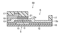
- the planarization film 18 is provided. However, as shown in FIG. 8, in the thin film transistor substrate 50, the planarization film 18 is not provided, and the interlayer insulating film 17 is used as a mask. It is good also as a structure which manufactures 50.
- the first to third photomasks 31 to 33 are used to form the gate electrode / gate.
- a wiring forming process, a gate insulating film forming process, a semiconductor layer forming process, a channel protective film forming process, and a source wiring / source electrode forming process are performed.
- an interlayer insulating film for example, a silicon nitride film, a silicon oxide film, a nitrided oxide film is formed on the entire substrate on which the source electrode 19 and the source wiring 16 are formed by plasma CVD. A silicon film or the like is formed.
- resist patterning, exposure and development by photolithography using a fourth photomask 34 having a predetermined pattern shape, exposure and development, and resist peeling and cleaning are performed on the silicon nitride film and the like, thereby forming the oxide semiconductor layer 13.
- the channel insulating film 21, the source electrode 19, and the source wiring 16 are covered, and the interlayer insulating film 17 in which the opening K is formed is formed.
- a predetermined etching gas for example, CF 4 gas and O 2 gas
- CF 4 gas and O 2 gas is used as the channel protective film removing step using the interlayer insulating film 17 as a mask.
- the channel protective film 21 in the opening K is removed by performing the dry etching.
- the oxide semiconductor layer 13 in the opening K is subjected to reducing plasma treatment to reduce the resistance of a part of the oxide semiconductor layer 13. Accordingly, a part of the oxide semiconductor layer 13 in the opening K functions as the drain electrode 13a, and a part of the oxide semiconductor layer 13 in the opening H functions as the pixel electrode 13b, so that the thin film transistor substrate shown in FIG. 50 is produced.
- the oxide semiconductor layer 13 made of indium gallium zinc oxide (IGZO) is used as the oxide semiconductor layer, but the oxide semiconductor layer 13 is not limited to this.
- IGZO indium gallium zinc oxide
- a metal containing at least one of indium (In), gallium (Ga), aluminum (Al), copper (Cu), zinc (Zn), magnesium (Mg), and cadmium (Cd) as an oxide semiconductor material An oxide material may be used.
- the oxide semiconductor layer 13 made of these oxide semiconductor materials has high mobility even if it is amorphous, the on-resistance of the switching element can be increased. Therefore, the difference in output voltage at the time of data reading becomes large, and the S / N ratio can be improved.
- oxide semiconductor films such as InGaO 3 (ZnO) 5 , Mg x Zn 1-x O, Cd x Zn 1-x O, and CdO can be given. it can.
- an oxide semiconductor layer is used as the semiconductor layer.
- the semiconductor layer is not limited to this, and instead of the oxide semiconductor layer, for example, a silicon-based semiconductor layer made of amorphous silicon or polysilicon. May be used as a semiconductor layer of a thin film transistor.
- Examples of utilization of the present invention include a method for manufacturing a thin film transistor substrate using an oxide semiconductor layer and a thin film transistor substrate manufactured by the method.
Landscapes
- Thin Film Transistor (AREA)
Abstract
Description
まず、ガラス基板やプラスチック基板等の絶縁基板10の基板全体に、スパッタリング法により、例えば、モリブテン膜(厚さ150nm程度)などを成膜する。その後、そのモリブテン膜に対して、所定のパターン形状を有する第1フォトマスク31を用いたフォトリソグラフィによるレジストのパターニング、ウエットエッチング及びレジストの剥離洗浄を行うことにより、図5(a)、図7(a)に示すように、絶縁基板10上に、ゲート配線11(図2参照)、ゲート電極15、及びゲート端子22を形成する。
次いで、ゲート配線11、ゲート電極15、ゲート端子22が形成された基板全体に、CVD法により、例えば、窒化シリコン膜(厚さ200nm~500nm程度)を成膜して、図5(b)、図7(b)に示すように、絶縁基板10上に、ゲート配線11、ゲート電極15、及びゲート端子22を覆うようにゲート絶縁膜12を形成する。
次いで、スパッタリング法により、例えば、酸化インジウムガリウム亜鉛(IGZO)により形成された酸化物半導体膜(厚さ30nm~100nm程度)を成膜し、図5(b)、図7(b)に示すように、ゲート絶縁膜12上に、酸化物半導体層13を形成する。
次いで、酸化物半導体層13が形成された基板全体に、プラズマCVD法により、例えば、窒化シリコン膜、酸化シリコン膜、窒化酸化シリコン膜などを成膜する。その後、その窒化シリコン膜等に対して、所定のパターン形状を有する第2フォトマスク32を用いたフォトリソグラフィによるレジストのパターニング、ウエットエッチング及びレジストの剥離洗浄を行うことにより、図5(c)に示すように、酸化物半導体層13上に、チャネル領域Cを覆うように、当該チャネル領域Cを保護するためのチャネル保護膜21を形成する。
次いで、酸化物半導体層13が形成された基板全体に、スパッタリング法により、例えば、チタン膜(厚さ30nm~150nm)及びアルミニウム膜(厚さ50nm~400nm程度)などを順に成膜する。
次いで、ソース電極19、及びソース配線16が形成された基板の全体に、プラズマCVD法により、例えば、窒化シリコン膜、酸化シリコン膜、窒化酸化シリコン膜などを成膜する。その後、図6(a)に示すように、酸化物半導体層13、チャネル保護膜21、ソース電極19、及びソース配線16を覆う層間絶縁膜17を厚さ250nm程度に形成する。なお、層間絶縁膜17は、単層構造に限定されず、2層構造や3層構造であっても良い。
次いで、層間絶縁膜17が形成された基板の全体に、スピンコート法又はスリットコート法により、感光性のアクリル樹脂等からなる感光性の有機絶縁膜を厚さ1.0μm~3.0μm程度に塗布する。
次いで、平坦化膜18をマスクとして、所定のエッチングガス(例えば、CF4ガスとO2ガス)を使用したドライエッチングを行い、層間絶縁膜17の一部を除去することにより、図6(b)に示すように、層間絶縁膜17及び平坦化膜18に開口部Hを形成する。
次いで、層間絶縁膜17及び平坦化膜18をマスクとして、シュウ酸を用いてエッチングを行うことにより、図7(e)に示すように、ゲート端子22が形成されたゲートドライバ領域Tgにおいて、ゲート絶縁膜12上に形成された酸化物半導体層13を除去する。
次いで、層間絶縁膜17及び平坦化膜18をマスクとして、所定のエッチングガス(例えば、CF4ガスとO2ガス)を使用したドライエッチングを行うことにより、図6(c)に示すように、開口部Hにおけるチャネル保護膜21を除去するとともに、図7(f)に示すように、ゲート端子22が形成されたゲートドライバ領域Tgにおいて、ゲート端子22上に形成されたゲート絶縁膜12を除去する。
次いで、開口部Hにおける酸化物半導体層13に対して還元性プラズマ処理を施し、酸化物半導体層13の一部を低抵抗化することにより、開口部Hにおける酸化物半導体層13の一部をドレイン電極13aとして機能させるとともに、開口部Hにおける酸化物半導体層13の一部を画素電極13bとして機能させ、図1~図4に示す薄膜トランジスタ基板1が作製される。
5 薄膜トランジスタ
10 絶縁基板
11 ゲート配線
12 ゲート絶縁膜
13 酸化物半導体層
13a ドレイン電極
13b 画素電極
15 ゲート電極
16 ソース配線
17 層間絶縁膜
18 平坦化膜
19 ソース電極
20 ソース端子
21 チャネル保護膜
22 ゲート端子
25 保護層
31 第1フォトマスク
32 第2フォトマスク
33 第3フォトマスク
34 第4フォトマスク
50 薄膜トランジスタ基板
C チャネル領域
H 開口部
K 開口部
Claims (6)
- 絶縁基板と、該絶縁基板上に設けられたゲート電極、該ゲート電極を覆うように設けられたゲート絶縁膜、該ゲート絶縁膜上に設けられ、チャネル領域を有する酸化物半導体層、及び該酸化物半導体層上に前記ゲート電極に重なるように設けられたソース電極を有する薄膜トランジスタと、前記チャネル領域を覆うように設けられたチャネル保護膜と、前記薄膜トランジスタを覆うように設けられた層間絶縁膜と、該層間絶縁膜を覆うように設けられた平坦化膜とを備えた薄膜トランジスタ基板の製造方法であって、
第1フォトマスクを用いて、前記絶縁基板上に前記ゲート電極を形成するゲート電極形成工程と、
前記絶縁基板上に、前記ゲート電極を覆うように前記ゲート絶縁膜を形成するゲート絶縁膜形成工程と、
前記ゲート絶縁膜上に、前記酸化物半導体層を形成する半導体層形成工程と、
第2フォトマスクを用いて、前記酸化物半導体層上に前記チャネル領域を覆うように前記チャネル保護膜を形成するチャネル保護膜形成工程と、
第3フォトマスクを用いて、前記酸化物半導体層上に前記ソース電極を形成するソース電極形成工程と、
前記酸化物半導体層、前記チャネル保護膜、及び前記ソース電極を覆う層間絶縁膜を形成する層間絶縁膜形成工程と、
第4フォトマスクを用いて、前記層間絶縁膜上に平坦化膜を形成する平坦化膜形成工程と、
前記平坦化膜をマスクとして用いて、前記層間絶縁膜の一部を除去することにより、前記層間絶縁膜及び前記平坦化膜に開口部を形成する開口部形成工程と、
前記層間絶縁膜及び前記平坦化膜をマスクとして、エッチングを行うことにより、前記開口部におけるチャネル保護膜を除去するチャネル保護膜除去工程と、
前記開口部における前記酸化物半導体層に対してプラズマ処理を施すプラズマ処理工程と
を少なくとも備えることを特徴とする薄膜トランジスタ基板の製造方法。 - 絶縁基板と、該絶縁基板上に設けられたゲート電極、該ゲート電極を覆うように設けられたゲート絶縁膜、該ゲート絶縁膜上に設けられ、チャネル領域を有する酸化物半導体層、及び該酸化物半導体層上に前記ゲート電極に重なるように設けられたソース電極を有する薄膜トランジスタと、前記チャネル領域を覆うように設けられたチャネル保護膜と、前記薄膜トランジスタを覆うように設けられた層間絶縁膜とを備えた薄膜トランジスタ基板の製造方法であって、
第1フォトマスクを用いて、前記絶縁基板上に前記ゲート電極を形成するゲート電極形成工程と、
前記絶縁基板上に、前記ゲート電極を覆うように前記ゲート絶縁膜を形成するゲート絶縁膜形成工程と、
前記ゲート絶縁膜上に、前記酸化物半導体層を形成する半導体層形成工程と、
第2フォトマスクを用いて、前記酸化物半導体層上に前記チャネル領域を覆うように前記チャネル保護膜を形成するチャネル保護膜形成工程と、
第3フォトマスクを用いて、前記酸化物半導体層上に前記ソース電極を形成するソース電極形成工程と、
第4フォトマスクを用いて、前記酸化物半導体層、前記チャネル保護膜、及び前記ソース電極を覆うとともに、開口部を有する層間絶縁膜を形成する層間絶縁膜形成工程と、
前記層間絶縁膜をマスクとして、エッチングを行うことにより、前記開口部におけるチャネル保護膜を除去するチャネル保護膜除去工程と、
前記開口部における前記酸化物半導体層に対してプラズマ処理を施すプラズマ処理工程と
を少なくとも備えることを特徴とする薄膜トランジスタ基板の製造方法。 - 前記プラズマ処理が、還元性プラズマ処理であることを特徴とする請求項1または請求項2に記載の薄膜トランジスタ基板の製造方法。
- 前記酸化物半導体層を形成する酸化物半導体材料が、インジウム(In)、ガリウム(Ga)、アルミニウム(Al)、銅(Cu)及び亜鉛(Zn)からなる群より選ばれる少なくとも1種を含む金属酸化物材料であることを特徴とする請求項1~請求項3のいずれか1項に記載の薄膜トランジスタ基板の製造方法。
- 前記酸化物半導体材料が、酸化インジウムガリウム亜鉛(IGZO)であることを特徴とする請求項4に記載の薄膜トランジスタ基板の製造方法。
- 請求項1~請求項5のいずれか1項に記載の製造方法により製造された薄膜トランジスタ基板。
Priority Applications (2)
| Application Number | Priority Date | Filing Date | Title |
|---|---|---|---|
| JP2012539580A JP5351341B2 (ja) | 2010-10-18 | 2011-10-11 | 薄膜トランジスタ基板の製造方法およびその方法により製造された薄膜トランジスタ基板 |
| US13/877,465 US9029209B2 (en) | 2010-10-18 | 2011-10-11 | Method of manufacturing a thin film transistor substrate and thin film transistor substrate manufactured by the same |
Applications Claiming Priority (2)
| Application Number | Priority Date | Filing Date | Title |
|---|---|---|---|
| JP2010233395 | 2010-10-18 | ||
| JP2010-233395 | 2010-10-18 |
Publications (1)
| Publication Number | Publication Date |
|---|---|
| WO2012053161A1 true WO2012053161A1 (ja) | 2012-04-26 |
Family
ID=45974892
Family Applications (1)
| Application Number | Title | Priority Date | Filing Date |
|---|---|---|---|
| PCT/JP2011/005681 Ceased WO2012053161A1 (ja) | 2010-10-18 | 2011-10-11 | 薄膜トランジスタ基板の製造方法およびその方法により製造された薄膜トランジスタ基板 |
Country Status (3)
| Country | Link |
|---|---|
| US (1) | US9029209B2 (ja) |
| JP (1) | JP5351341B2 (ja) |
| WO (1) | WO2012053161A1 (ja) |
Cited By (2)
| Publication number | Priority date | Publication date | Assignee | Title |
|---|---|---|---|---|
| WO2014069316A1 (ja) * | 2012-10-31 | 2014-05-08 | シャープ株式会社 | エレクトロルミネッセンス基板およびその製造方法、エレクトロルミネッセンス表示パネル、エレクトロルミネッセンス表示装置 |
| JP2014232824A (ja) * | 2013-05-30 | 2014-12-11 | 三菱電機株式会社 | 薄膜トランジスタ、表示パネル用基板、表示パネル、表示装置および薄膜トランジスタの製造方法 |
Citations (2)
| Publication number | Priority date | Publication date | Assignee | Title |
|---|---|---|---|---|
| JP2006100760A (ja) * | 2004-09-02 | 2006-04-13 | Casio Comput Co Ltd | 薄膜トランジスタおよびその製造方法 |
| JP2010141230A (ja) * | 2008-12-15 | 2010-06-24 | Renesas Electronics Corp | 半導体装置及び半導体装置の製造方法 |
Family Cites Families (2)
| Publication number | Priority date | Publication date | Assignee | Title |
|---|---|---|---|---|
| US7982215B2 (en) * | 2005-10-05 | 2011-07-19 | Idemitsu Kosan Co., Ltd. | TFT substrate and method for manufacturing TFT substrate |
| JP5123141B2 (ja) | 2008-11-19 | 2013-01-16 | 株式会社東芝 | 表示装置 |
-
2011
- 2011-10-11 US US13/877,465 patent/US9029209B2/en not_active Expired - Fee Related
- 2011-10-11 WO PCT/JP2011/005681 patent/WO2012053161A1/ja not_active Ceased
- 2011-10-11 JP JP2012539580A patent/JP5351341B2/ja not_active Expired - Fee Related
Patent Citations (2)
| Publication number | Priority date | Publication date | Assignee | Title |
|---|---|---|---|---|
| JP2006100760A (ja) * | 2004-09-02 | 2006-04-13 | Casio Comput Co Ltd | 薄膜トランジスタおよびその製造方法 |
| JP2010141230A (ja) * | 2008-12-15 | 2010-06-24 | Renesas Electronics Corp | 半導体装置及び半導体装置の製造方法 |
Cited By (5)
| Publication number | Priority date | Publication date | Assignee | Title |
|---|---|---|---|---|
| WO2014069316A1 (ja) * | 2012-10-31 | 2014-05-08 | シャープ株式会社 | エレクトロルミネッセンス基板およびその製造方法、エレクトロルミネッセンス表示パネル、エレクトロルミネッセンス表示装置 |
| CN104769658A (zh) * | 2012-10-31 | 2015-07-08 | 夏普株式会社 | 电致发光基板及其制造方法、电致发光显示面板、电致发光显示装置 |
| EP2916310A4 (en) * | 2012-10-31 | 2015-11-18 | Sharp Kk | ELECTROLUMINESCENT SUBSTRATE, PROCESS FOR THE PRODUCTION THEREOF, ELECTROLUMINESCENT DISPLAY PANEL AND ELECTROLUMINESCENT DISPLAY DEVICE |
| JPWO2014069316A1 (ja) * | 2012-10-31 | 2016-09-08 | シャープ株式会社 | エレクトロルミネッセンス基板およびその製造方法、エレクトロルミネッセンス表示パネル、エレクトロルミネッセンス表示装置 |
| JP2014232824A (ja) * | 2013-05-30 | 2014-12-11 | 三菱電機株式会社 | 薄膜トランジスタ、表示パネル用基板、表示パネル、表示装置および薄膜トランジスタの製造方法 |
Also Published As
| Publication number | Publication date |
|---|---|
| JPWO2012053161A1 (ja) | 2014-02-24 |
| US20130187155A1 (en) | 2013-07-25 |
| US9029209B2 (en) | 2015-05-12 |
| JP5351341B2 (ja) | 2013-11-27 |
Similar Documents
| Publication | Publication Date | Title |
|---|---|---|
| JP5209146B2 (ja) | 半導体装置およびその製造方法 | |
| TWI538222B (zh) | 半導體裝置 | |
| JP5855752B2 (ja) | 半導体装置およびその製造方法 | |
| JP5275519B2 (ja) | 表示装置用基板及びその製造方法、表示装置 | |
| JP4958253B2 (ja) | 薄膜トランジスタ | |
| US8624238B2 (en) | Thin-film transistor substrate and method of fabricating the same | |
| JP5347071B2 (ja) | アクティブマトリクス基板の製造方法及びその方法により製造されたアクティブマトリクス基板、並びに表示パネル | |
| US10134910B2 (en) | Semiconductor device and production method therefor | |
| US20120241750A1 (en) | Semiconductor device and method for producing same | |
| JP2008311616A (ja) | 薄膜トランジスタ表示板及びその製造方法 | |
| WO2012032749A1 (ja) | 薄膜トランジスタ基板及びその製造方法、表示装置 | |
| TWI416736B (zh) | 薄膜電晶體及其製造方法 | |
| WO2011104791A1 (ja) | 薄膜トランジスタ基板及びその製造方法、表示装置 | |
| CN112420849A (zh) | 金属氧化物薄膜晶体管及其制作方法 | |
| CN104576760A (zh) | 薄膜晶体管及其制备方法、阵列基板和显示装置 | |
| KR20160129160A (ko) | 박막 트랜지스터 표시판 및 그 제조 방법 | |
| JP5558222B2 (ja) | 薄膜トランジスタ基板の製造方法 | |
| WO2015049818A1 (ja) | 薄膜トランジスタ基板の製造方法 | |
| JP5351341B2 (ja) | 薄膜トランジスタ基板の製造方法およびその方法により製造された薄膜トランジスタ基板 | |
| CN115084277A (zh) | 金属氧化物薄膜晶体管及其制作方法、阵列基板 | |
| CN107004603B (zh) | 半导体装置及其制造方法 | |
| WO2013008441A1 (ja) | アクティブマトリクス基板及びその製造方法 | |
| CN117476667B (zh) | 阵列基板和阵列基板的制备方法 | |
| CN116072680A (zh) | 薄膜晶体管阵列基板及其制作方法和显示面板 | |
| CN115036271A (zh) | 金属氧化物半导体薄膜晶体管阵列基板及其制作方法、显示装置 |
Legal Events
| Date | Code | Title | Description |
|---|---|---|---|
| 121 | Ep: the epo has been informed by wipo that ep was designated in this application |
Ref document number: 11834007 Country of ref document: EP Kind code of ref document: A1 |
|
| WWE | Wipo information: entry into national phase |
Ref document number: 2012539580 Country of ref document: JP |
|
| WWE | Wipo information: entry into national phase |
Ref document number: 13877465 Country of ref document: US |
|
| NENP | Non-entry into the national phase |
Ref country code: DE |
|
| 122 | Ep: pct application non-entry in european phase |
Ref document number: 11834007 Country of ref document: EP Kind code of ref document: A1 |