WO2012043670A1 - 太陽電池および太陽電池モジュール - Google Patents
太陽電池および太陽電池モジュール Download PDFInfo
- Publication number
- WO2012043670A1 WO2012043670A1 PCT/JP2011/072263 JP2011072263W WO2012043670A1 WO 2012043670 A1 WO2012043670 A1 WO 2012043670A1 JP 2011072263 W JP2011072263 W JP 2011072263W WO 2012043670 A1 WO2012043670 A1 WO 2012043670A1
- Authority
- WO
- WIPO (PCT)
- Prior art keywords
- solar cell
- electrode
- layer
- underlayer
- base layer
- Prior art date
- Legal status (The legal status is an assumption and is not a legal conclusion. Google has not performed a legal analysis and makes no representation as to the accuracy of the status listed.)
- Ceased
Links
Images



Classifications
-
- H—ELECTRICITY
- H10—SEMICONDUCTOR DEVICES; ELECTRIC SOLID-STATE DEVICES NOT OTHERWISE PROVIDED FOR
- H10F—INORGANIC SEMICONDUCTOR DEVICES SENSITIVE TO INFRARED RADIATION, LIGHT, ELECTROMAGNETIC RADIATION OF SHORTER WAVELENGTH OR CORPUSCULAR RADIATION
- H10F77/00—Constructional details of devices covered by this subclass
- H10F77/20—Electrodes
- H10F77/206—Electrodes for devices having potential barriers
- H10F77/211—Electrodes for devices having potential barriers for photovoltaic cells
-
- Y—GENERAL TAGGING OF NEW TECHNOLOGICAL DEVELOPMENTS; GENERAL TAGGING OF CROSS-SECTIONAL TECHNOLOGIES SPANNING OVER SEVERAL SECTIONS OF THE IPC; TECHNICAL SUBJECTS COVERED BY FORMER USPC CROSS-REFERENCE ART COLLECTIONS [XRACs] AND DIGESTS
- Y02—TECHNOLOGIES OR APPLICATIONS FOR MITIGATION OR ADAPTATION AGAINST CLIMATE CHANGE
- Y02E—REDUCTION OF GREENHOUSE GAS [GHG] EMISSIONS, RELATED TO ENERGY GENERATION, TRANSMISSION OR DISTRIBUTION
- Y02E10/00—Energy generation through renewable energy sources
- Y02E10/50—Photovoltaic [PV] energy
Definitions
- the present invention relates to a solar cell and a solar cell module.
- an electrode manufactured by a plating method is known as an electrode of a solar cell.
- FIG. 15 is a cross-sectional view of a conventional solar cell.
- a solar cell includes an electrically insulating substrate 101, and a lower electrode 102 made of ITO (indium oxide) or the like, an n-type semiconductor layer 103, an i-type semiconductor layer 104, and a p-type semiconductor layer 105 on the substrate 101.
- the upper electrode 108 made of a conductive paste is present in the entire region under the current collecting electrode 109, the stress related to heat shrinkage due to the upper electrode 108 is increased, and the current collecting is thus performed.
- the electrode 109 may be peeled off.
- the solar cell of the present invention includes an electrode provided on one main surface of a semiconductor substrate, and a base layer provided on at least a part under the electrode, and the electrode is provided on the base layer and the base layer. It is formed on a portion that does not have a base layer.
- electrode peeling can be suppressed.
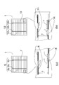
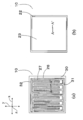
- FIG.1 (a) is a figure for demonstrating arrangement
- FIG.1 (b) is embodiment based on this invention. It is a figure for demonstrating arrangement
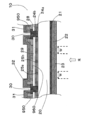
- FIG. 2 is a cross-sectional view taken along a dotted line A-A ′ in FIGS.
- FIG. 2 is a cross-sectional view taken along a dotted line B-B ′ in FIGS.
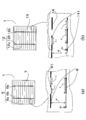
- FIG. 4 (a) is a plan view of the surface side of a solar cell according to the second embodiment of the present invention and a diagram for explaining the arrangement of the underlayer, and FIG.
- FIG. 4 (b) is a second embodiment according to the present invention. It is a figure for demonstrating arrangement
- FIG. 5A is a plan view of the surface side of a solar cell according to a third embodiment of the present invention and a diagram for explaining the arrangement of the underlayer, and
- FIG. 5B is a third embodiment according to the present invention. It is a figure for demonstrating arrangement
- FIG. 6A is a plan view of the surface side of a solar cell according to a fourth embodiment of the present invention and a diagram for explaining the arrangement of the underlayer, and FIG.
- FIG. 6B is a fourth embodiment according to the present invention. It is a figure for demonstrating arrangement
- FIG. 7 (a) is a plan view of the surface side of a solar cell according to a fifth embodiment of the present invention and a diagram for explaining the arrangement of the underlayer, and
- FIG. 7 (b) is a fifth embodiment according to the present invention. It is a figure for demonstrating arrangement
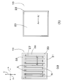
- FIG. 9A is a plan view of the back surface side of the solar cell according to the seventh embodiment of the present invention
- FIG. 9B is a plan view of the front surface side of the solar cell according to the seventh embodiment of the present invention.
- FIG. 10 is a cross-sectional view of the solar cell along A-A ′ in FIGS. 9 (a) and 9 (b).
- FIG. 10A is a plan view of the back surface side of the solar cell according to the eighth embodiment
- FIG. 10B is a plan view of the front surface side of the solar cell.
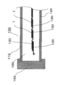
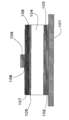
- FIG. 12 is a cross-sectional view of the solar cell along A-A ′ in FIGS. 11 (a) and 11 (b). It is a top view of the solar cell module which is each embodiment concerning the present invention.
- FIG. 14 is a partial cross-sectional view along A-A ′ of FIG. 13. It is sectional drawing which showed the conventional solar cell.
- FIG. 1A is a diagram for explaining a plan view of the surface side of the solar cell and the arrangement of the underlayer
- FIG. 1B is a plan view of the back surface side of the solar cell and the arrangement of the underlayer
- FIG. 2 is a sectional view taken along the dotted line AA ′ in FIGS. 1A and 1B
- FIG. 3 is a sectional view taken along the dotted line BB ′ in FIGS. 1A and 1B.
- reference numeral 1 denotes a solar cell, on the first main surface having the texture structure of the n-type single crystal silicon substrate 2, an i-type amorphous silicon layer 3 having a thickness of 5 nm to 20 nm and a p-type amorphous having a thickness of 5 nm to 20 nm.
- a surface-side electrode 6 including a plurality of finger electrodes 6 a arranged in parallel to each other and two bus bar electrodes 6 b perpendicular to these is formed.
- an insulating layer 7 containing a transparent resin having a thickness of 20 ⁇ m, for example, an acrylic resin is formed.
- This insulating layer 7 functions as an antireflection layer or a protective layer. Further, when the surface side electrode 6 is formed by electrolytic plating, the insulating layer 7 functions as a mask layer.
- a silver powder as a thermosetting conductive paste having a thickness of 20 ⁇ m and a length of 2 mm is formed between the transparent conductive layer 5 and the end portion T1 which is the peripheral side of the solar cell 1 of the plurality of finger electrodes 6a.
- the finger electrodes 6a are linear with a thickness of 20 ⁇ m and a width of 50 ⁇ m, respectively, and are arranged at intervals of 2 mm, and the bus bar electrodes 6b are linear with a thickness of 20 ⁇ m and a width of 1 mm, respectively.
- a transparent conductive film layer 11 made of ITO (indium oxide) containing (tin) is formed in this order.
- a back side electrode 12 composed of a plurality of finger electrodes 12 a arranged in parallel to each other and two bus bar electrodes 12 b orthogonal to these, and the back side electrode
- An insulating layer 13 containing, for example, a transparent resin having a thickness of 20 ⁇ m, for example, an acrylic resin, is formed around 12. This insulating layer 13 also has the same function as the insulating layer 7.
- the finger electrodes 12a are linear with a thickness of 20 ⁇ m and a width of 50 ⁇ m, respectively, and are arranged at intervals of 2 mm.
- the bus bar electrodes 12b are linear with a thickness of 20 ⁇ m and a width of 1 mm, respectively.
- the edge part side part T2 which is the circumference
- variety of the finger electrode 12a A conductive underlayer 14 formed by curing a silver paste containing a thermosetting resin and a silver powder as a thermosetting conductive paste is interposed. That is, the base layer 14 having a good adhesion between the transparent conductive film layer 11 and the finger electrodes 12a is present just below the end portion 15 of the plurality of finger electrodes 12a. In the present embodiment, each base layer 14 does not exist below the end of each finger electrode 12a, and is formed approximately 0.5 to 2 mm away from the end.
- the surface side electrode 6 has a Ni / Cu / Ni three-layer structure including a Ni layer having a thickness of 5 ⁇ m as a first layer, a Cu layer having a thickness of 10 ⁇ m as a second layer, and a Ni layer having a thickness of 5 ⁇ m as a third layer.
- the surface is rounded so as to cover the periphery of the opening of the insulating layer 7 on the transparent conductive film layer 5 and the base layer 8.
- the back electrode 12 also has a Ni / Cu / Ni three-layer structure consisting of a Ni layer having a thickness of 5 ⁇ m as the first layer, a Cu layer having a thickness of 10 ⁇ m as the second layer, and a Ni layer having a thickness of 5 ⁇ m as the third layer.
- the surface has a roundness so as to cover the periphery of the opening of the insulating layer 13 on the conductive film layer 11 and the base layer 14.
- the texture structure is a random texture structure, and a large number of pyramid shapes are irregularly arranged.
- the pyramid shape has irregular heights (sizes), and adjacent pyramids are not identical. There may be overlapping.
- the top of each pyramid-shaped convex part and the valley bottom part of the recessed part between each pyramid may be rounded.
- the maximum height difference (the height difference between the top point of the convex portion on the surface and the bottom point of the concave portion) t1 of the unevenness constituting the texture structure is the maximum height difference (the height between the top point and the bottom point) of the underlayers 8 and 14. Difference) t2 or less.
- the maximum height difference (the height difference between the top point of the convex portion on the surface and the bottom point of the concave portion) t1 has, for example, 15 ⁇ m
- the maximum height difference (the height difference between the top point and the bottom point) t2 is For example, it has 20 ⁇ m.
- the substrate 2 is, for example, a substantially square of about 125 mm square and a thickness of 100 ⁇ m to 300 ⁇ m.
- each base layer 8 has a large adhesive force between each finger electrode 6a and the transparent conductive film layer 5, and its volume is reduced in order to reduce the stress caused by each base layer 8.
- the provided part is the edge part side which may become a starting point of peeling of each finger electrode 6a, peeling of each finger electrode 6a can be suppressed.
- the underlayer 9 contains a resin, the stress is relaxed.
- each finger electrode 12a can be suppressed by each base layer 14.
- the front surface side electrode 6 and the back surface side electrode 12 are formed so as to cover the periphery of the opening portions of the insulating layers 7 and 13, respectively, moisture and impurities are emitted from the opening portions of the insulating layers 7 and 13 to the sun. It is possible to prevent the battery 1 from entering.
- an n-type silicon single crystal substrate 2 is prepared, and a random texture structure is formed over the entire surface of the n-type silicon single crystal substrate 2 by wet etching using an etchant made of an alkaline aqueous solution, and facing each other.
- An n-type silicon single crystal substrate 2 having first and second main surfaces having a random texture structure is prepared.
- the i-type amorphous silicon layer 3 and the p-type amorphous silicon layer 4 are formed in this order on the first main surface of the n-type silicon single crystal substrate 2 by CVD (chemical vapor deposition) or the like.
- the i-type amorphous silicon layer 9 and the n-type amorphous silicon layer 10 are formed in this order on the second main surface of the n-type silicon single crystal substrate 2.
- the transparent conductive film layer 5 is formed over the entire upper surface of the p-type amorphous silicon layer 4 by sputtering or ion plating, and the transparent conductive film layer 11 is formed over the entire upper surface of the n-type amorphous silicon layer 10.
- the insulating layer 7 is formed by spin coating or the like using a photo-curing transparent resin having a predetermined viscosity over the entire upper surface of the transparent conductive film layer 5 and cured by ultraviolet rays.
- the insulating layer 13 is formed by spin coating or the like using a photo-curing transparent resin having a predetermined viscosity and cured with ultraviolet rays over the entire upper surface of the film layer 11.
- the insulating layer 7 is irradiated with ultraviolet rays using a photomask at a predetermined portion, the insulating layer 7 is developed with an organic solvent to form an opening X corresponding to the electrode pattern, and a photomask is used at the predetermined portion.
- the insulating layer 13 is irradiated with ultraviolet light, and the insulating layer 13 is developed with a predetermined solvent to form an opening corresponding to the electrode pattern.
- a silver paste is printed on the transparent conductive film layer 5 exposed by the opening X in the region of the end side portion that is the peripheral side of the solar cell 1 by a screen printing method or the like, and cured to form the underlayer 8.
- a silver paste is printed by a screen printing method or the like on the transparent conductive film layer 11 on the end side portion that is the peripheral side of the solar battery cell 1 of the opening X, and is cured to form the base layer 14.
- FIG. 4A is a plan view for explaining the arrangement of the surface side of the solar cell and the base layer
- FIG. 4B is a plan view for explaining the arrangement of the back side of the solar cell and the base layer. is there. Note that differences from the first embodiment will be mainly described. The same parts as those of the first embodiment will not be described, and the same or similar parts as those of the first embodiment will be denoted by the same reference numerals.
- the second embodiment is different from the first embodiment in the position of the underlying layer, and has a thickness of 20 ⁇ m and a length between the transparent conductive film layer and the plurality of finger electrodes 6a and 12a. It is the same in that a conductive underlayer formed by curing a thermosetting conductive paste having a thickness of 2 mm is interposed.
- the base layer 8 is present only directly below the end portion on the peripheral side of the solar cell 1 among the plurality of finger electrodes 6a, and the base layer 14 is directly below the plurality of finger electrodes 12a. Among these, it exists only under the edge part which is the circumference side of the solar cell 1.
- FIG. 5A is a plan view of the front surface side of the solar cell and a diagram for explaining the arrangement of the underlayer
- FIG. 5B is a plan view of the back surface side of the solar cell and a diagram for explaining the arrangement of the underlayer. It is. Note that differences from the first embodiment will be mainly described. The same parts as those of the first embodiment will not be described, and the same or similar parts as those of the first embodiment will be denoted by the same reference numerals.
- the underlayers 8 and 14 exist only immediately below the end portions of the finger electrodes 6a and 12a of the front surface side electrode 6 and the back surface side electrode 12,
- the underlying layers 8 and 14 are regularly and discretely arranged immediately below the front surface side electrode 6 and the back surface side electrode 12, and the transparent conductive film is interposed between the transparent conductive film layer 5 and the front surface side electrode 6.
- a conductive underlayer formed by curing the thermosetting conductive paste is interposed between the layer 11 and the back surface side electrode 12.
- the conductive paste is the same as that in the first embodiment.
- a conductive base layer 8 formed by curing a thermosetting conductive paste having a width of 50 ⁇ m, a thickness of 20 ⁇ m, and a length S of 2 mm immediately below each finger electrode 6a has an interval L of 2 mm, etc.
- the pitches are provided at intervals, and are also arranged directly below the end portions of the finger electrodes 6a.
- the underlying layer 8 of the finger electrode 6a and each underlying layer 8 of the adjacent finger electrode 6a are opposed to each other, and the interval L between the underlying layers 8 and the interval L between the adjacent underlying layers 8 are arranged to oppose each other. Yes.
- conductive base layers 8 formed by curing a thermosetting conductive paste having a width of 1 mm, a thickness of 20 ⁇ m, and a length S of 2 mm are provided at equal intervals with an interval L of 2 mm. It is also arranged immediately below the end of each bus bar electrode 6b.
- the underlayer 8 is regularly and discretely arranged below the finger electrode 6a including directly under the end of the finger electrode 6a that may be a peeling base point, the finger electrode 6a Can be further suppressed.
- the base layer 8 is regularly and discretely arranged under the bus bar electrode 6b including the portion immediately below the end portion of the bus bar electrode 6b, peeling of the bus bar electrode 6b can be suppressed.
- peeling of the surface electrode 6 can be suppressed by the underlayer 14 regularly and discretely arranged in the entire region directly below the surface side electrode 6 in this way.
- the underlying layer 14 that is regularly and discretely arranged in the entire region directly below the back surface side electrode 12 can suppress the peeling of the finger electrodes 12a and the bus bar electrodes 12b, that is, the back surface side electrode 12, as compared with the first embodiment. .
- the length S and the interval L of the underlayer 8 are the same, but the length S of the underlayer 8 may be larger than the interval L. In this case, peeling of the electrode can be further suppressed by the length S of the underlayer 8 being large.
- the underlayer 8 is disposed directly below the bus bar electrode 6b of the front side electrode 6. However, the underlayer 8 may be omitted. In particular, when the bus bar electrode 6b is wide, Since the risk of peeling is lower than that of the substrate 8, the underlayer 8 may not be provided.
- FIG. 6A is a plan view of the front surface side of the solar cell and a diagram for explaining the arrangement of the underlayer
- FIG. 6B is a plan view of the back surface side of the solar cell and the arrangement of the underlayer. is there. Note that differences from the third embodiment will be mainly described.
- the underlying layers 8 and 14 of the finger electrodes 6a and 12a and the underlying layers 8 and 14 of the adjacent finger electrodes 6a and 12a are opposed to each other, and the finger electrode 6a. , 12a and the adjacent finger electrodes 6a, 12a are arranged so as to face each other.
- the finger electrodes 6a, 12a adjacent to the underlying layer 8 of the finger electrodes 6a, 12a are arranged. The points are regularly arranged so that the distances L of each other face each other.
- the length S of the base layers 8 and 14 of the finger electrodes 6a and 12a is set to be larger than the interval L.
- the length S is 2 mm and the interval L is 1 mm.
- FIG. 7A is a plan view of the surface side of the solar cell and a diagram for explaining the arrangement of the underlayer
- FIG. 7B is a plan view of the back side of the solar cell and the arrangement of the underlayer. is there. Note that differences from the fourth embodiment will be mainly described.
- thermosetting conductive paste is the same as that in the fourth embodiment.
- the length S and the interval L of the base layers 8 and 14 of the finger electrodes 6a and 12a are the same, for example, 2 mm.
- the second underlayers 81 and 141 are the same as the underlayers 8 and 14 except that the length S2 is 0.2 mm.
- FIG. 8 is a cross-sectional view of a solar cell. Note that differences from the third embodiment will be mainly described.
- the underlying layer is divided by the unevenness of the transparent conductive films 5 and 14 reflecting the texture structure of the first and second main surfaces of the n-type single crystal silicon substrate 2.
- the base layer is arranged so as to be discretely and dispersedly arranged immediately below the front surface side electrode 6 and directly below the back surface side electrode 12.
- the transparent layer is transparent between the transparent conductive film layer 5 and the front surface side electrode 6.
- a conductive underlayer formed by curing a thermosetting paste is interposed between the conductive film layer 11 and the back surface side electrode 12.
- the thermosetting paste is the same as that in the third embodiment.
- the underlying layers 8 and 14 in which the hardened conductive paste present in the concave portion of the texture structure and divided by the convex portion is irregularly and discretely arranged.
- the base layers 8 and 14 are formed by thinly forming a thermosetting conductive paste on the transparent conductive films 5 and 14 reflecting the texture structure so that at least the tips of the convex portions of the texture structure are exposed, and then thermosetting.
- the underlying layers 8 and 14 are formed in which the cured thermosetting conductive paste divided according to the texture structure is irregularly and discretely arranged.
- the maximum height difference (the height difference between the uppermost point of the convex portion on the surface and the lowermost point of the concave portion) t1 is equal to or greater than the maximum height difference (the height difference between the uppermost point and the lowest point) t2 of the underlayers 8 and 14. .
- the maximum height difference (the height difference between the top point of the convex portion on the surface and the bottom point of the concave portion) t1 has a height difference of 15 ⁇ m
- the maximum height difference (the height difference between the top point and the bottom point) t2 is It has a height difference of 10 ⁇ m.
- the hardened conductive paste constituting the base layers 8 and 14 is configured to be present in each recess of the texture structure, the volume of the hardened conductive paste can be reduced. 14 can be reduced, and peeling of the front surface electrode 6 and the rear surface side electrode 12 can be suppressed by the base layer discretely disposed in the entire region immediately below the front surface side electrode 6 and the rear surface side electrode 12.
- FIGS. 9A and 10 A back junction solar cell according to a seventh embodiment of the present invention will be described with reference to FIGS. 9 and 10.
- 9A is a plan view of the back side of the solar cell
- FIG. 9B is a plan view of the front side of the solar cell
- FIG. 10 is a solar cell along AA ′ in FIGS. 9A and 9B.
- FIG. 9A is a plan view of the back side of the solar cell
- FIG. 9B is a plan view of the front side of the solar cell
- FIG. 10 is a solar cell along AA ′ in FIGS. 9A and 9B.
- reference numeral 10 denotes a solar cell, which is an i-type having a thickness of several to 250 mm on the first main surface on the light incident surface side having the texture structure (not shown) of the n-type single crystal silicon substrate 20.
- the amorphous silicon layer 21, the n-type amorphous silicon 22 having a thickness of about 20 to 500 mm, the antireflection layer made of silicon oxide, silicon nitride, silicon oxynitride and the like having a thickness of about 80 nm to 1 ⁇ m and the insulating layer 23 functioning as a protective layer are provided. Formed in order.
- the p-type electrode formation region 24 and the n-type electrode formation region 25 are formed in a comb-tooth shape on the second main surface which is the back surface opposite to the light incident surface of the solar cell 10, and the p-type electrode
- the finger-shaped portions 26 of the formation region 24 and the finger-shaped portions 27 of the n-type electrode formation region 25 are alternately arranged along a direction X perpendicular to the direction Y in the drawing.
- the p-type electrode formation region 24 includes an i-type amorphous silicon layer 24a having a thickness of several to 250 mm and a p-type amorphous silicon layer 24b having a thickness of 20 to 500 mm.
- a transparent conductive film layer 28 made of ITO containing, for example, Sn (tin) having a thickness of 50 nm to 200 nm is formed.
- the n-type electrode formation region 25 includes an i-type amorphous silicon layer 25a having a thickness of several to 250 mm and an n-type amorphous silicon layer 25b having a thickness of 20 to 500 mm.
- a transparent conductive film layer 29 made of ITO containing, for example, Sn (tin) having a thickness of 50 nm to 200 nm is formed.
- the p-type electrode formation region 24 and the n-type electrode formation region 25 are separated by an insulating layer 30 having a thickness of 10 to 30 ⁇ m formed on the transparent conductive film layers 28 and 29.
- a base layer 92 made of a hardened metal paste made of silver paste or the like is placed on the insulating layer 30. It is formed so as to cover the part.
- a base layer 92 formed by curing a metal paste made of silver paste or the like forms the insulating layer 30. It is formed so as to cover the part.
- the first and second electrodes 31 and 32 have the base layer 92 formed by curing a conductive paste made of silver paste or the like immediately below the end X of the finger-shaped portions 27 and 26.
- the first and second electrodes 31 and 32 can be prevented from peeling off the transparent conductive film layers 28 and 29.
- the electrodes 31 and 32 are formed so as to cover the transparent conductive film layers 28 and 29 exposed at the opening of the insulating layer 30, impurities such as moisture are introduced from the opening of the insulating layer 30 into the solar cell 10. You can prevent getting inside.
- the p-type electrode formation region 24 and the n-type electrode formation region 25 have an i-type amorphous layer, but may be configured without an i-type amorphous layer.
- the p-type amorphous silicon layer 24b and the n-type amorphous silicon layer 25b may be formed by a diffusion method.
- an n-type silicon single crystal substrate 20 is prepared, and an n-type in which a random texture structure is formed by wet etching with an etchant made of NaOH aqueous solution only on the entire first main surface of the n-type silicon single crystal substrate 20.
- a silicon single crystal substrate 20 is prepared.
- an i-type amorphous silicon layer 21, an n-type amorphous silicon 22 and an insulating layer 23 are formed on the first main surface of the n-type single crystal silicon substrate 20 by a CVD method or the like.
- a p-type electrode formation region 24 and an n-type electrode formation region 25 are formed in a predetermined region on the second main surface of the n-type silicon single crystal substrate 20.
- the p-type electrode formation region 24 is formed by forming the i-type amorphous silicon layer 24a and the p-type amorphous silicon 24b on the second main surface in this order through a predetermined metal mask by a CVD method or the like.
- the transparent conductive film layer 28 is formed on the p-type amorphous silicon 24 through a metal mask by an ion plating method.
- the n-type electrode formation region 25 is formed by forming the i-type amorphous silicon layer 25a and the n-type amorphous silicon 25b on the second main surface in this order through a predetermined metal mask by a CVD method or the like.
- the transparent conductive film layer 29 is formed on the n-type amorphous silicon 25b through a metal mask by an ion plating method.
- an insulating layer 30 made of resin such as acrylic resin is formed on the entire area of the n-type single crystal silicon substrate 20 on which the p-type electrode formation region 24 and the n-type electrode formation region 25 are formed. Then, after irradiating a predetermined portion on the insulating layer 30 with ultraviolet light using a photomask, the insulating layer 30 is developed with an organic solvent to form a predetermined opening corresponding to the electrode shape in the insulating layer 30.
- FIGS. 11 and 12 A back junction solar cell according to a seventh embodiment of the present invention will be described with reference to FIGS. 11 and 12.
- 11A is a plan view of the back surface side of the solar cell
- FIG. 11B is a plan view of the front surface side of the solar cell
- FIG. 12 is a cross-sectional view taken along the line AA ′ of FIGS. 11A and 11B. It is. Note that differences from the seventh embodiment will be mainly described, and the same or similar parts as those in the sixth embodiment are denoted by the same reference numerals.
- the eighth embodiment is different from the seventh embodiment in that the base layer is formed under the end of the finger-shaped portion of the first electrode 31 and the finger shape of the second electrode 32.
- a plurality of points are discretely formed on the p-type electrode formation region 24 below the first electrode 31 and the n-type electrode formation region 25 below the second electrode 32 as well as below the end of the portion.
- the dotted line in Fig.14 (a) has shown the position of the base layer.
- a plurality of columns are formed on the p-type electrode formation region 24 below the first electrode 31 and on the n-type electrode formation region 25 below the second electrode 32 along their extending direction (longitudinal direction).
- three rows of dotted base layers 950 and 960 are formed, and the three rows of dotted base layers 950 and 960 are the central base layer 960 and the transparent conductive film layers 28 and 29). It is formed only on the top, and two rows of base layers 950 at both ends are formed on the transparent conductive film layers 28 and 29 so as to cover a part of the insulating layer 30.
- the base layer 950,960 obtained by curing the metal paste which is a silver paste constituting the dotted base layer 950,960, has a pitch interval W of 50 ⁇ m to 0.1 mm.
- the underlying layer 950 partially in the region where the first and second electrodes 31, 32 are formed on the transparent conductive film layers 28, 29 exposed in the opening of the insulating layer 30 (not shown). 960 is formed.
- a plurality of base layers 950 and 960 made of a hardened metal paste are discretely arranged so as to cover substantially the entire area under the first electrode 31 and the second electrode 32. Moreover, peeling of the 1st electrode 31 and the 2nd electrode 32 can be suppressed rather than 7th Embodiment.
- the solar cell module which is embodiment concerning this invention is demonstrated using FIG.13 and FIG.14. 13 is a top view of the solar cell module, and a cross-sectional view taken along the line AA ′ of FIG. 13 in FIG.
- reference numeral 100 denotes a solar cell module including a plurality of solar cells 1 according to the first to sixth embodiments.
- the solar cell module 100 is a transparent surface side such as white tempered glass.
- a weather-resistant back side cover 120 made of a resin film such as polyethylene terephthalate (PET)
- PET polyethylene terephthalate
- a linear solar cell group 140 electrically connected in series by a strip-shaped connecting member 130 made of a flat copper wire or the like whose surface is coated with a solder layer such as Pb is filled with ethylene vinyl acetate (EVA) or the like.
- EVA ethylene vinyl acetate
- It consists of a plate-like structure that is arranged via a material 150 and a metal frame 160 made of aluminum or the like that supports the structure.
- the solar cell groups 140 are arranged in parallel to each other, and the connection member 130 on one end side of each predetermined adjacent solar cell group 140 is a solder layer so that all the solar cell groups 140 are electrically connected in series. Solder connection is performed by a strip-shaped connection member 170 made of an applied flat copper wire or the like, and the connection member 130 on the other end side of another predetermined adjacent solar cell group 140 is covered with a solder layer. Solder-connected to L-shaped connecting members 180 and 190 made of flat copper wire or the like. With this configuration, the plurality of solar cells 1 of the solar cell module 100 are arranged in a matrix.
- a flat copper wire having a surface coated with a solder layer for taking out an electric output from the solar cell module 100 is connected to the connecting member 130 of the solar cell 1 at both ends on the power extraction side in the outermost solar cell group 140.
- L-shaped connection members (output extraction connection members) 200 and 210 made of solder or the like are connected by soldering.
- the front end portions of the L-shaped connecting member 180, the L-shaped connecting member 190, the L-shaped connecting member 200, and the L-shaped connecting member 210 are notched in the back cover 120. Is led into a terminal box located in the upper center of the back side of the solar cell module 100.
- the sun disposed between the front surface side cover 110 and the back surface side cover 120 via the filler 150. It is comprised from the plate-shaped structure formed by electrically connecting between the batteries 10 with a connection member, and the metal frame 160 which consists of aluminum etc. which support a structure.
- the base layer was a base layer formed by curing a thermosetting conductive paste containing a metal powder and a thermosetting resin, but the base layer is not limited to a silver paste, gold,
- the conductive paste may be prepared by using a conductive paste containing a powder of metal such as copper or carbon, or an alloy thereof and a resin, and a resin. Is preferred.
- the base layer is not limited to the thermosetting conductive paste, and may be a base layer manufactured using a photocurable conductive paste, or a base layer made of a metal film made of chromium or titanium having high adhesion. Furthermore, if it is 1st, 2nd embodiment etc., it is also possible to use the base layer which consists of resin which does not have electroconductivity instead.
- both the front surface side electrode and the back surface side electrode have bus bar electrodes, but may be bus barless without bus bar electrodes.
- a random texture structure is used as the texture structure, but a texture structure having regular irregularities may be used.
- the electrode is formed by an electrolytic plating method, but may be formed by a sputtering method, a vapor deposition method, or the like.
- the present invention is not limited to the structure of the solar cell, and can be applied to various solar cells such as a polycrystalline solar cell.
Landscapes
- Photovoltaic Devices (AREA)
Abstract
【課題】 【解決手段】 半導体基板2の一主面上に電極6を有する太陽電池1であって、電極6下の前記一主面の少なくとも一部上に設けられた下地層9を有し、電極6は、下地層9上及び下地層9を有していない部分上に形成されている。
Description
本発明は、太陽電池および太陽電池モジュールに関する。
太陽電池の電極として、従来、メッキ法により製造された電極が知られている。
図15を参照して、従来のメッキ法による電極を供えた太陽電池について説明する。図15は従来の太陽電池の断面図である。
図中、太陽電池は、電気絶縁性の基板101と、基板101上には、ITO(酸化インジウム)等からなる下部電極102、n型半導体層103、i型半導体層104、p型半導体層105、ITO等からなる透明電極106、光透過性の高分子樹脂からなるパッシベーション層107、導電性ペーストからなる上部電極108及び電解メッキ法により形成された集電電極109をこの順で備える。
しかしながら、斯かる従来の太陽電池では、導電性ペーストからなる上部電極108が集電電極109下の全域に存在するため、この上部電極108に起因して熱収縮に関わる応力が大きくなり、集電電極109が剥離する恐れがある。
本発明の太陽電池は、半導体基板の一主面上に設けられた電極と、前記電極下の少なくとも一部上に設けられた下地層と、を備え、前記電極は、前記下地層上及び前記下地層を有していない部分上に形成されている。
本発明では、電極の剥れを抑制できる。
(第1実施形態)
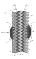
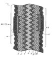
本発明に係る第1の実施形態である太陽電池について図面を用いて詳細に説明する。図1(a)は太陽電池の表面側平面図及び下地層の配置を説明するための図であり、図1(b)は太陽電池の裏面側平面図及び下地層の配置を説明するための図である。また、図2は図1(a)、(b)の点線A-A’に沿った断面図であり、図3は図1(a)、(b)の点線B-B’に沿った断面図である。
本発明に係る第1の実施形態である太陽電池について図面を用いて詳細に説明する。図1(a)は太陽電池の表面側平面図及び下地層の配置を説明するための図であり、図1(b)は太陽電池の裏面側平面図及び下地層の配置を説明するための図である。また、図2は図1(a)、(b)の点線A-A’に沿った断面図であり、図3は図1(a)、(b)の点線B-B’に沿った断面図である。
図中、1は太陽電池であり、n型単結晶シリコン基板2のテクスチャー構造を有する第1の主面上に、厚み5nm~20nmのi型アモルファスシリコン層3、厚み5nm~20nmのp型アモルファスシリコン層4、及び厚み70μm~100nmの例えばSn(錫)を含有するITO(酸化インジウム)からなる透明導電膜層5がこの順序に形成されている。透明導電膜層5上には、互いに平行に配置されてなる複数のフィンガー電極6aとこれらと直交してなる2本のバスバー電極6bとからなる表面側電極6が形成されている。表面側電極6の周囲には、例えば、厚み20μmの透明な樹脂、例えばアクリル樹脂を含有してなる絶縁層7が形成されている。
この絶縁層7は、反射防止層や保護層として機能する。また、表面側電極6を電解メッキ法で形成する場合は、絶縁層7はマスク層として機能する。
ここで、透明導電膜層5と複数のフィンガー電極6aの太陽電池1の周囲側である端部側部分T1の間には、厚み20μm、長さ2mmの熱硬化型導電性ペーストとしての銀粉末と熱硬化型樹脂を含有してなる銀ペーストが硬化してなる導電性の下地層8がそれぞれ介在している。即ち、複数のフィンガー電極6aの直下のうち、その端部側部分T1の直下のみに透明導電膜層5とフィンガー電極6aとの付着性が良好な下地層8が存在する。なお、本実施形態では、各下地層8は、各フィンガー電極6aの端下には存在せず、該端から0.5~2mm程度離間して形成されている。
フィンガー電極6aは、それぞれ厚み20μm、幅50μmの直線状であって、互いに2mm間隔で配置されており、バスバー電極6bは、それぞれ厚み20μm、幅1mmの直線形状である。
また、基板2のテクスチャー構造を有する第2の主面上には、厚み5nm~20nmのi型アモルファスシリコン層9、厚み10nm~50nmのn型アモルファスシリコン層10、及び厚み70μm~100nmの例えばSn(錫)を含有するITO(酸化インジウム)からなる透明導電膜層11がこの順序に形成されている。透明導電膜層11上には、互いに平行に配置されてなる複数のフィンガー電極12aとこれらと直交してなる2本のバスバー電極12bからなる裏面側電極12が形成されていると共に、裏面側電極12の周囲には、例えば、厚み20μmの透明な樹脂、例えばアクリル樹脂を含有してなる絶縁層13が形成されている。この絶縁層13も、絶縁層7と同じ機能を有する。
フィンガー電極12aは、それぞれ厚み20μm、幅50μmの直線状であって、互いに2mm間隔で配置されており、バスバー電極12bは、それぞれ厚み20μm、幅1mmの直線形状である。
ここで、太陽電池1の周囲側である端部側部分T2において、透明導電膜層11と複数のフィンガー電極12aとの間には厚み20μm、長さ2mm、フィンガー電極12aの幅と同じ幅の熱硬化型導電性ペーストとしての銀粉末と熱硬化型樹脂を含有してなる銀ペーストが硬化して形成される導電性の下地層14がそれぞれ介在している。即ち、複数のフィンガー電極12aの直下のうち、その端部側部分15の直下のみに、透明導電膜層11とフィンガー電極12aとの付着力が良好な下地層14が存在する。なお、本実施形態では、各下地層14は、各フィンガー電極12aの端下には存在せず、端から0.5~2mm程度離間して形成されている。
本実施形態では、表面側電極6は、一層目として厚み5μmのNi層、二層目として10μmのCu層、三層目として厚み5μmのNi層からなるNi/Cu/Niの三層構造からなり、透明導電膜層5上及び下地層8上に絶縁層7の開口部の周囲を覆うように表面が丸みを有している。
また、裏面側電極12も、一層目として厚み5μmのNi層、二層目として10μmのCu層、三層目として厚み5μmのNi層からなるNi/Cu/Niの三層構造からなり、透明導電膜層11上及び下地層14上に絶縁層13の開口部の周囲を覆うように表面が丸みを有している。
本実施形態では、前記テクスチャー構造はランダムテクスチャー構造であって、多数のピラミッド形状が不規則に配置しており、ピラミッド形状は、その高さ(大きさ)が不揃いであり、隣り合うピラミッドが一部重なりあってもよい。なお、各ピラミッド形状の凸部の頂上部および各ピラミッド間の凹部の谷底部は、丸みを帯びていてもよい。
上記テクスチャー構造を構成する凹凸の最大高低差(表面の凸部の最上点と凹部の最下点の高低差)t1は、下地層8、14の最大高低差(最上点と最下点の高低差)t2以下である。ここで、最大高低差(表面の凸部の最上点と凹部の最下点の高低差)t1は、例えば15μmを有し、最大高低差(最上点と最下点の高低差)t2は、例えば20μmを有している。
基板2は、例えば、約125mm角の略正方形、厚み100μm~300μmである。
本実施形態の太陽電池セルでは、各下地層8は各フィンガー電極6aと透明導電膜層5との付着力が大きく、且つ各下地層8に起因する応力を低減するためにその体積を小さくなるように各フィンガー電極6a下に部分的に設けられる。また、その設けられている部分が各フィンガー電極6aの剥離の起点となる恐れのある端部側であるので、各フィンガー電極6aの剥離を抑制できる。しかも、下地層9は樹脂を含むため応力緩和がなされる。
また、同様に、各下地層14により各フィンガー電極12aの剥離を抑制できる。
本実施形態では、表面側電極6及び裏面側電極12がそれぞれ絶縁層7,13の開口部の周囲を覆うように形成されているので、水分や不純物が絶縁層7,13の開口部から太陽電池1中に入るのを防止できる。
次に、本実施形態の太陽電池の製造方法を説明する。
最初に、図示しないが、n型シリコン単結晶基板2を用意し、n型シリコン単結晶基板2の表面全域にアルカリ水溶液からなるエッチング液を用いたウェットエッチングによりランダムテクスチャー構造を形成し、互いに対向するランダムテクスチャー構造を有する第1、第2の主面を有するn型シリコン単結晶基板2を準備する。
次に、CVD法(化学気相成長法)等により、n型シリコン単結晶基板2の第1の主面上に、i型アモルファスシリコン層3及びp型アモルファスシリコン層4をこの順序で形成すると共に、n型シリコン単結晶基板2の第2の主面上に、i型アモルファスシリコン層9及びn型アモルファスシリコン層10をこの順序で形成する。
その後、スパッタ法又はイオンプレーティング法によりp型アモルファスシリコン層4の上面の全域上に透明導電膜層5を形成すると共に、n型アモルファスシリコン層10の上面の全域上に、透明導電膜層11を形成する。
次に、透明導電膜層5の上面の全域上に所定の粘度を有し、紫外線で硬化する光硬化性の透明な樹脂を用いてスピンコート法等により絶縁層7を形成すると共に、透明導電膜層11の上面の全域上に所定の粘度を有し、紫外線で硬化する光硬化性の透明な樹脂を用いてスピンコート法等により絶縁層13を形成する。
その後、所定部分にフォトマスクを用いて紫外線を絶縁層7に照射し、有機溶剤により絶縁層7を現像して電極パターンに対応する開口部Xを形成すると共に、所定部分にフォトマスクを用いて紫外線光を絶縁層13に照射し、所定の溶剤により絶縁層13を現像して電極パターンに対応する開口部を形成する。
次に、太陽電池1の周囲側である端部側部分の領域において、開口部Xにより露出した透明導電膜層5上に、スクリーン印刷法等により銀ペーストを印刷し、硬化させて下地層8を形成すると共に、前記開口部Xの太陽電池セル1の周囲側である端部側部分の透明導電膜層11上に、スクリーン印刷法等により銀ペーストを印刷し、硬化させて下地層14を形成する。
そして、開口部を備えた絶縁層7、13をマスク層として、該開口部に露出した透明導電膜層5、11上及び下地層8、14上にそれぞれ表面側電極6及び裏面側電極12を電解メッキ法により形成して太陽電池セル1を完成する。
(第2実施形態)
本発明にかかる第2の実施形態である太陽電池について図4を参照しながら詳細に説明する。図4(a)は太陽電池の表面側平面図および下地層の配置を説明するための図、図4(b)は太陽電池の裏面側平面図および下地層の配置を説明するための図である。なお、第1実施形態との相違点について主に説明し、第1実施形態と同一部分は説明を割愛し、第1実施形態と同一または類似部分には同一符号を付している。
(第2実施形態)
本発明にかかる第2の実施形態である太陽電池について図4を参照しながら詳細に説明する。図4(a)は太陽電池の表面側平面図および下地層の配置を説明するための図、図4(b)は太陽電池の裏面側平面図および下地層の配置を説明するための図である。なお、第1実施形態との相違点について主に説明し、第1実施形態と同一部分は説明を割愛し、第1実施形態と同一または類似部分には同一符号を付している。
図4を参照して、第2実施形態において、第1実施形態との相違点は、下地層の配置位置であり、透明導電膜層と複数のフィンガー電極6a,12aの間に厚み20μm、長さ2mmの熱硬化型導電性ペーストが硬化してなる導電性の下地層が介在している点は同じである。
本実施形態では、下地層8は複数のフィンガー電極6aの直下のうち、太陽電池1の周囲側である端部の直下のみに存在し、また下地層14は、複数のフィンガー電極12aの直下のうち、太陽電池1の周囲側である端部の直下のみに存在する。
本実施形態では、各フィンガー電極6a,12aの剥離の起点となる太陽電池1の周囲側の端部下に各下地層8,14が存在するので、各フィンガー電極6a,12aの剥離をより抑制できる。
(第3実施形態)
本発明にかかる第3実施形態である太陽電池について、図5を参照して説明する。図5(a)は太陽電池の表面側平面図及び下地層の配置を説明するための図、図5(b)は太陽電池の裏面側平面図及びおよび下地層の配置を説明するための図である。なお、第1実施形態との相違点について主に説明し、第1実施形態と同一部分は説明を割愛し、第1実施形態と同一または類似部分には同一符号を付している。
(第3実施形態)
本発明にかかる第3実施形態である太陽電池について、図5を参照して説明する。図5(a)は太陽電池の表面側平面図及び下地層の配置を説明するための図、図5(b)は太陽電池の裏面側平面図及びおよび下地層の配置を説明するための図である。なお、第1実施形態との相違点について主に説明し、第1実施形態と同一部分は説明を割愛し、第1実施形態と同一または類似部分には同一符号を付している。
第1実施形態との相違点は、第1実施形態では、下地層8,14が表面側電極6及び裏面側電極12のフィンガー電極6a,12aの端部側の直下のみに存在するが、本実施形態では、下地層8,14が表面側電極6及び裏面側電極12の直下に規則正しく離散的に配置されている点であり、透明導電膜層5と表面側電極6の間、透明導電膜層11と裏面側電極12間に熱硬化型導電性ペーストが硬化してなる導電性の下地層が介在している点は同じである。なお、導電性ペーストは第1実施形態と同じものである。
本実施形態では、各フィンガー電極6a直下において、幅50μm、厚み20μm、長さSが2mmの熱硬化型導電性ペーストが硬化してなる導電性の下地層8が、間隔Lが2mmでの等間隔のピッチで設けられており、各フィンガー電極6aの端部の直下にも配置されている。
また、フィンガー電極6aの下地層8と隣り合うフィンガー電極6aの各下地層8は互いに対向し、下地層8の間隔Lと隣り合う下地層8の間隔Lとは互いに対向するように配置されている。
バスバー電極6b直下において、幅1mm、厚み20μm、長さSが2mmの熱硬化型導電性ペーストが硬化してなる導電性の下地層8が、間隔Lが2mmでの等間隔のピッチで設けられており、各バスバー電極6bの端部の直下にも配置されている。
また、一方のバスバー電極6bの下地層8と対向する他方のバスバー電極6bの各下地層8は互いに対向し、一方の下地層8の間隔Lと他方の下地層8の間隔Lは互いに対向するように配置されている。
本実施形態の太陽電池1では、下地層8が剥離の基点となる恐れのあるフィンガー電極6aの端部の直下を含めフィンガー電極6aの下に規則正しく離散的に配置されているため、フィンガー電極6aの剥離をより抑制できる。
また、下地層8がバスバー電極6bはその端部の直下を含めバスバー電極6bの直下にも規則正しく離散的に配置されているので、バスバー電極6bの剥離が抑制できる。
従って、このように表面側電極6の直下全域に規則正しく離散的に配置されている下地層14により表面電極6の剥離を抑制できる。
また、同様に、裏面側電極12の直下全域に規則正しく離散的に配置されている下地層14により、フィンガー電極12a、バスバー電極12b、即ち裏面側電極12の剥離を第1実施形態よりも抑制できる。
上述では、下地層8の長さSと間隔Lを同じにしているが、下地層8の長さSを間隔Lより大きくしてもよい。この場合、下地層8の長さSが大きいことにより、電極の剥離をより抑制できる。
上述では、表面側電極6のバスバー電極6bの直下にも下地層8を配置させているが、下地層8を設けないようにもでき、特にバスバー電極6bが幅広の場合は、細線状の場合に比べて剥離の恐れが低いので、下地層8を設けないようにしてもよい。
また、裏面側電極12のバスバー電極12bの下地層14についても同様に設けないようにもしてもよい。
(第4実施形態)
本発明にかかる第4実施形態である太陽電池について、図6を参照して説明する。図6(a)は太陽電池の表面側平面図及び下地層の配置を説明するための図、図6(b)は太陽電池の裏面側平面図及び下地層の配置を説明するための図である。なお、第3実施形態との相違点について主に説明する。
(第4実施形態)
本発明にかかる第4実施形態である太陽電池について、図6を参照して説明する。図6(a)は太陽電池の表面側平面図及び下地層の配置を説明するための図、図6(b)は太陽電池の裏面側平面図及び下地層の配置を説明するための図である。なお、第3実施形態との相違点について主に説明する。
第3実施形態との相違点は、第3実施形態では、フィンガー電極6a,12aの下地層8,14と隣り合うフィンガー電極6a,12aの下地層8,14とは互いに対向し、フィンガー電極6a,12aの間隔Lと隣り合うフィンガー電極6a,12aの間隔Lは互いに対向するように配置されているが、本実施形態では、フィンガー電極6a,12aの下地層8と隣り合うフィンガー電極6a,12aの間隔Lが対向するように規則正しく配置されている点である。
また、本実施形態では、各フィンガー電極6a,12aの下地層8,14の長さSは、間隔Lより大きく設定されており、例えば、長さSは2mm、間隔Lは1mmである。
フィンガー電極6a,12aの端部の直下にも配置されている。
本実施形態では、下地層8,14上に比べて下地層8,14が存在しない間隔L上の付着強度が弱いため、フィンガー電極6a,12aのうち、間隔L上の部分の電気的な接触状態が悪くなり、間隔L上の部分でのキャリア収集が低下しても、L上の部分と下地層8,14とが第3実施例に比べて近く存在するので、フィンガー電極6a,12aの下地層8,14上の部分でキャリア収集ができる。
(第5実施形態)
本発明にかかる第5実施形態である太陽電池について、図7を参照して説明する。図7(a)は太陽電池の表面側平面図及び下地層の配置を説明するための図、図7(b)は太陽電池の裏面側平面図及び下地層の配置を説明するための図である。なお、第4実施形態との相違点について主に説明する。
(第5実施形態)
本発明にかかる第5実施形態である太陽電池について、図7を参照して説明する。図7(a)は太陽電池の表面側平面図及び下地層の配置を説明するための図、図7(b)は太陽電池の裏面側平面図及び下地層の配置を説明するための図である。なお、第4実施形態との相違点について主に説明する。
第4実施形態との相違点は、本実施形態では、間隔Lの中央部に導電性の第2の下地層を更に設ける点であり、この下地層も透明導電膜層5と表面側電極6の間、透明導電膜層11と裏面側電極12間に熱硬化型導電性ペーストが硬化してなる導電性の下地層が介在している点は同じである。なお、熱硬化型導電性ペーストは第4実施形態と同じものである。
本実施形態では、フィンガー電極6a,12aの下地層8,14の長さSと間隔Lは同じであり、例えば、2mmである。
第2の下地層81、141は、長さS2が0.2mmである他は、下地層8,14と同じである。
この場合は、下地層の材料を低減しつつ、第4実施形態と類似の効果が得られる。
(第6実施形態)
本発明にかかる第6実施形態である太陽電池について、図8を参照して説明する。図8は太陽電池の断面図である。なお、第3実施形態との相違点について主に説明する。
(第6実施形態)
本発明にかかる第6実施形態である太陽電池について、図8を参照して説明する。図8は太陽電池の断面図である。なお、第3実施形態との相違点について主に説明する。
第3実施形態と異なる点は、本実施形態では、n型単結晶シリコン基板2の第1,2の主面のテクスチャー構造を反映した透明導電膜5,14の凹凸により、下地層を分断し、下地層が表面側電極6の直下及び裏面側電極12の直下に離散的、分散的に配置するように構成している点であり、透明導電膜層5と表面側電極6の間、透明導電膜層11と裏面側電極12間に熱硬化型ペーストが硬化してなる導電性の下地層が介在している点は同じである。なお、熱硬化型ペーストは第3実施形態と同じものである。
本実施形態では、テクスチャー構造の凹部に存在し、凸部により分断された硬化した導電性ペーストが非規則的で離散的に配置されてなる下地層8,14を有する。
下地層8,14は、例えば、テクスチャー構造を反映した透明導電膜5,14上に熱硬化型導電性ペーストをテクスチャー構造の凸部の先端部分が少なくとも露出するように薄く形成した後、熱硬化型導電性ペーストを硬化させることにより、テクスチャー構造に対応して分断された当該硬化した熱硬化型導電性ペーストが非規則的で離散的に配置されてなる下地層8,14を形成する。
前記凹凸の最大高低差(表面の凸部の最上点と凹部の最下点の高低差)t1は下地層8,14の最大高低差(最上点と最下点の高低差)t2以上である。例えば、最大高低差(表面の凸部の最上点と凹部の最下点の高低差)t1は、15μmの高低差を有し、最大高低差(最上点と最下点の高低差)t2は、10μmの高低差を有している。
本実施形態では、下地層8,14を構成する硬化した導電性ペーストがテクスチャー構造の各凹部に存在するように構成しているので、硬化した導電性ペーストの体積を小さくでき、下地層8,14に起因する応力を低減できると共に、表面側電極6及び裏面側電極12の直下全域に離散的に配置されている下地層により表面電極6及び裏面側電極12の剥離を抑制できる。
また、本実施形態の太陽電池セルは、上述した様に、上記各実施形態に比べ、容易に製造が可能である。
(第7実施形態)
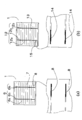
図9及び図10を用いて本発明にかかる第7実施形態である裏面接合型太陽電池について説明する。図9(a)は太陽電池の裏面側平面図、図9(b)は太陽電池の表面側平面図、図10は図9(a)、(b)のA-A’に沿った太陽電池の断面図である。
(第7実施形態)
図9及び図10を用いて本発明にかかる第7実施形態である裏面接合型太陽電池について説明する。図9(a)は太陽電池の裏面側平面図、図9(b)は太陽電池の表面側平面図、図10は図9(a)、(b)のA-A’に沿った太陽電池の断面図である。
図中、10は太陽電池であり、n型単結晶シリコン基板20のテクスチャー構造(図示せず)を有する光入射面側である第1の主面上に、厚み数Å~250Å程のi型アモルファスシリコン層21、及び厚み20Å~500Å程度のn型アモルファスシリコン22、厚み80nm~1μm程度の酸化ケイ素、窒化ケイ素、酸窒化ケイ素等からなる反射止層及び保護層として機能する絶縁層23がこの順序で形成されている。
また、太陽電池10の光入射面とは反対側の裏面となる第2の主面上に、p型電極形成領域24及びn型電極形成領域25がくし歯状に形成されており、p型電極形成領域24のフィンガー形状部分26とn型電極形成領域25のフィンガー形状部分27は図中の方向Yに垂直な方向Xに沿って交互に配列される。
p型電極形成領域24は、厚み数Å~250Åのi型アモルファスシリコン層24a及び厚み20Å~500Åのp型アモルファスシリコン層24bで構成されている。p型アモルファスシリコン層24b上には、厚み50nm~200nmの例えばSn(錫)を含有するITOからなる透明導電膜層28が形成されている。
n型電極形成領域25は、厚み数Å~250Åのi型アモルファスシリコン層25a及び厚み20Å~500Åのn型アモルファスシリコン層25bで構成されている。n型アモルファスシリコン層25b上には、厚み50nm~200nmの例えばSn(錫)を含有するITOからなる透明導電膜層29が形成されている。
p型電極形成領域24とn型電極形成領域25は、透明導電膜層28,29上に形成された厚み10~30μmからなる絶縁層30によって分離されている。
p型電極形成領域24の透明導電膜層28上には、厚み5μmのNi層、厚み10μmのCu層、及び厚み5μmのNi層がこの順序で電解メッキ法により作製された第1の電極31が形成されている。
ここで、第1の電極31のフィンガー形状部分26の端部Xの直下の透明導電膜層28上には、銀ペースト等からなる金属ペーストが硬化されてなる下地層92が絶縁層30を一部覆うように形成されている。
n型電極形成領域25の透明導電膜層29上には、厚み5μmのNi層、厚み10μmのCu層、及び厚み5μmのNi層がこの順序で電解メッキ法により作製された第2の電極32が形成されている。
ここで、第2の電極32のフィンガー形状部分27の端部Xの直下の透明導電膜層29上には、銀ペースト等からなる金属ペーストが硬化されてなる下地層92が絶縁層30を一部覆うように形成されている。
本実施形態でも、第1,第2の電極31,32は、フィンガー形状部分27,26の端部Xの直下に、銀ペースト等からなる導電性ペーストが硬化されてなる下地層92を有するので、第1,第2の電極31,32が透明導電膜層28,29から剥れるのを防止できる。
また、電極31,32は、絶縁層30の開口部に露出した透明導電膜層28,29上に覆うように形成されているので、絶縁層30の開口部より水分等の不純物が太陽電池10中に入るのを防止できる。
上述では、p型電極形成領域24及びn型電極形成領域25は、i型アモルファス層を有するが、i型アモルファス層を備えない構成とすることもできる。この構成の場合、拡散法によりp型アモルファスシリコン層24b、n型アモルファスシリコン層25bを形成してもよい。
次に、本実施形態に係る太陽電池セルの製造方法について説明する。
最初に、n型シリコン単結晶基板20を用意し、n型シリコン単結晶基板20の第1の主面上の全域のみにNaOH水溶液からなるエッチング液によるウェットエッチングによりランダムテクスチャー構造を形成したn型シリコン単結晶基板20を準備する。
その後、n型単結晶シリコン基板20の第1の主面上には、CVD法等により、i型アモルファスシリコン層21、n型アモルファスシリコン22、絶縁層23を形成する。
次に、n型シリコン単結晶基板20の第2の主面上の所定領域にp型電極形成領域24及びn型電極形成領域25を形成する。
p型電極形成領域24は、CVD法等により所定の金属マスクを介して前記第2の主面上にi型アモルファスシリコン層24a、p型アモルファスシリコン24bをこの順序で形成した後、スパッタ法又はイオンプレーティング法により金属マスクを介してp型アモルファスシリコン24上に透明導電膜層28を形成して作製される。
n型電極形成領域25は、CVD法等により所定の金属マスクを介して前記第2の主面上にi型アモルファスシリコン層25a、n型アモルファスシリコン25bをこの順序で形成した後、スパッタ法又はイオンプレーティング法により金属マスクを介してn型アモルファスシリコン25b上に透明導電膜層29を形成して作製される。
次に、p型電極形成領域24及びn型電極形成領域25が形成されたn型単結晶シリコン基板20の全域上にアクリル樹脂等の樹脂からなる絶縁層30を形成する。その後、この絶縁層30上の所定部分にフォトマスク用いて紫外線光を照射した後、有機溶剤により絶縁層30を現像して絶縁層30に電極形状に対応した所定の開口部を形成する。
次に、絶縁層30の上記開口部から露出した透明導電膜層28,29上の第1の電極31のフィンガー形状部分の端部および第2の電極32のフィンガー形状部分の端部に位置する部分に銀ペーストをスクリーン印刷により形成し、これらを硬化して下地層92を作製する。
最後に、上記開口部から露出した透明導電膜28、29及び下地層92上に電解メッキ法により第1、第2の電極31、32をそれぞれ形成する。
(第8実施形態)
図11及び図12を用いて、本発明にかかる第7実施形態である裏面接合型太陽電池について説明する。図11(a)は太陽電池の裏面側平面図、図11(b)は太陽電池の表面側平面図、図12は図11(a),(b)のA-A’に沿った断面図である。なお、第7実施形態との相違点について主に説明し、第6実施形態と同一または類似部分には同一符号を付している。
(第8実施形態)
図11及び図12を用いて、本発明にかかる第7実施形態である裏面接合型太陽電池について説明する。図11(a)は太陽電池の裏面側平面図、図11(b)は太陽電池の表面側平面図、図12は図11(a),(b)のA-A’に沿った断面図である。なお、第7実施形態との相違点について主に説明し、第6実施形態と同一または類似部分には同一符号を付している。
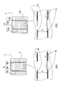
図11~図12を参照して、第8実施形態において、第7実施形態との相違点は、下地層が第1の電極31のフィンガー形状部分の端部下および第2の電極32のフィンガー形状部分の端部下のみでなく、第1の電極31下のp型電極形成領域24上および第2の電極32下のn型電極形成領域25上に複数離散的に形成されている点である。なお、図14(a)中の点線は下地層の位置を示している。
本実施形態では、第1の電極31下のp型電極形成領域24上および第2の電極32下のn型電極形成領域25上に、それらの延存方向(長手方向)に沿って複数列(本実施形態では3列)の点線状の下地層950,960が形成されており、3列の点線状の下地層950,960は、中央列の下地層960が透明導電膜層28,29上にのみ形成されると共に、両端の2列の下地層950が絶縁層30の一部を覆うように透明導電膜層28,29上に形成されている。ここで、点線状の下地層950,960を構成する銀ペーストである金属ペーストが硬化されてなる下地層950,960は、ピッチ間隔Wが50μm~0.1mmである。
本実施形態では、図示していない絶縁層30の開口部に露出した透明導電膜層28,29上の第1、2の電極31,32を形成している領域に部分的に下地層950,960を形成している。
本実施形態では、第1の電極31下および第2の電極32下の略全域を覆うように、硬化してなる金属ペーストからなる複数の下地層950,960が離散的に配置されているので、第1の電極31および第2の電極32の剥離を第7実施形態よりも抑制できる。
(太陽電池モジュール)
図13及び図14を用いて、本発明にかかる実施形態である太陽電池モジュールについて説明する。図13は太陽電池モジュールの上面図、図14の図13のA-A’に沿った断面図である。
(太陽電池モジュール)
図13及び図14を用いて、本発明にかかる実施形態である太陽電池モジュールについて説明する。図13は太陽電池モジュールの上面図、図14の図13のA-A’に沿った断面図である。
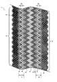
図13~図14を参照して、100は、第1~第6実施形態に係る太陽電池1を複数備えた太陽電池モジュールであり、太陽電池モジュール100は、白板強化ガラス等の透明な表面側カバー110、ポリエチレンテレフタレート(PET)等の樹脂フィルムからなる耐候性の裏面側カバー120、および表面側カバー110と裏面側カバー120の間に、複数の太陽電池1がSn-Ag-CuやSn-Pb等の半田層で表面が被覆されてなる平板銅線等からなるストリップ状の接続部材130により電気的に直列接続されてなる直線状の太陽電池群140がエチレンビニルアセテート(EVA)等の充填材150を介して配置されてなる板状の構成体と、構成体を支持するアルミニウム等からなる金属製枠体160から構成されている。
太陽電池群140は互いに並列に配置され、全ての太陽電池群140が電気的に直列接続するように、各所定の隣り合う太陽電池群140の一方端側の接続部材130が半田層で表面が被着された平板銅線等からなるストリップ状の接続部材170によって半田接続されると共に、他の所定の隣り合う太陽電池群140の他方端側の接続部材130が半田層で表面が被覆された平板銅線等からなるL字状の接続部材180,190と半田接続されている。この構成により、太陽電池モジュール100の複数の太陽電池1はマトリックス状に配置される。
最外側の太陽電池群140中の電力取り出し側の両最端の太陽電池1の接続部材130には、太陽電池モジュール100から電気出力を取り出すための半田層で表面が被着された平板銅線等からなるL字状の接続部材(出力取り出し用接続部材)200,210がそれぞれ半田接続されている。
また、図示しないが、L字状の接続部材180、L字状の接続部材190、L字状の接続部材200およびL字状の接続部材210の各先端部分は、裏面側カバー120の切り欠きを介して太陽電池モジュール100の裏面側の上部中央に位置する端子ボックス内に導かれている。
第7~第8実施形態に係る裏面接合型太陽電池10を用いた太陽電池モジュールの場合も、例えば、表面側カバー110と裏面側カバー120の間に充填材150を介して配置されてなる太陽電池10間が接続部材で電気的に接続してなる板状の構成体と、構成体を支持するアルミニウム等からなる金属製枠体160から構成される。
上記各実施形態において、下地層としては、金属粉末と熱硬化型樹脂を含有する熱硬化型導電性ペーストを硬化してなる下地層であったが、下地層は銀ペーストに限らず、金、銅、炭素等の金属又はこれらの合金の粉末と樹脂を含有した導電性ペーストを用いて作製してもよい、導電性ペーストは、樹脂、樹脂のバインダー、バインダーの溶剤を混合し、ペースト状としたものが好ましい。
また、熱硬化型導電性ペーストに限らず、光硬化型導電性ペーストを用いて作製した下地層でもよく、付着性の高いクロムやチタン等からなる金属膜からなる下地層でもよい。
更には、第1,第2実施形態等であれば、導電性を有しない樹脂からなる下地層を代わりに用いることも可能である。
更には、第1,第2実施形態等であれば、導電性を有しない樹脂からなる下地層を代わりに用いることも可能である。
また、第1~第6実施形態では、表面側電極、裏面側電極ともバスバー電極を有する電極であったが、バスバー電極を有さないバスバーレスとしてもよい。
上記各実施形態では、テクスチャー構造として、ランダムテクスチャー構造を用いたが、規則正しい凹凸を有するテクスチャー構造としてもよい。
また、本実施形態の電極では、電解メッキ法により電極を形成したが、スパッタ法、蒸着法等により形成してもよい。
また、第1~第6実施形態では、両面受光型の太陽電池の例を示したが、本発明は、片面受光型の太陽電池にも適用できる。
本発明は、上記太陽電池の構造に限定されず、多結晶太陽電池等の種々の太陽電池に適用可能である。
1、10 太陽電池セル
8、14、91、92、950、960 下地層
8、14、91、92、950、960 下地層
Claims (11)
- 半導体基板の一主面上に設けられた電極と、
前記電極下の少なくとも一部上に設けられた下地層と、を備え、
前記電極は、前記下地層上及び前記下地層を有していない部分上に形成されている、太陽電池。 - 前記下地層が前記半導体基板の端部側部分に配置されている請求項1記載の太陽電池。
- 前記下地層が離散的に配置されている請求項1記載の太陽電池
- 前記下地層は規則正しく配置されている請求項1~3のいずれか1項に記載の太陽電池。
- 前記下地層は不規則に配置されている請求項1~3のいずれか1項に記載の太陽電池。
- 前記電極は複数のフィンガー形状部を有し、前記下地層は前記半導体基板の周囲側の前記フィンガー形状部下の端部側に配置されている請求項1~5のいずれか1項に記載の太陽電池。
- 前記下地層は前記電極下の全域上に配置されている請求項1に記載の太陽電池。
- 前記一主面はテクスチャー構造を有する面であり、前記下地層は前記テクスチャー構造の凹凸の前記凹内に設けられている請求項1~請求項7のいずれか1項に記載の太陽電池。
- 前記下地層は、硬化してなる導電性ペースト又は金属から形成されている請求項1~請求項8のいずれか1項に記載の太陽電池。
- 前記下地層は、その上下の面に対して良付着性を有する請求項1~9のいずれか1項に記載の太陽電池。
- 請求項1~10いずれか1項に記載の太陽電池を備えた太陽電池モジュール。
Applications Claiming Priority (2)
| Application Number | Priority Date | Filing Date | Title |
|---|---|---|---|
| JP2010-222905 | 2010-09-30 | ||
| JP2010222905 | 2010-09-30 |
Publications (1)
| Publication Number | Publication Date |
|---|---|
| WO2012043670A1 true WO2012043670A1 (ja) | 2012-04-05 |
Family
ID=45893109
Family Applications (1)
| Application Number | Title | Priority Date | Filing Date |
|---|---|---|---|
| PCT/JP2011/072263 Ceased WO2012043670A1 (ja) | 2010-09-30 | 2011-09-28 | 太陽電池および太陽電池モジュール |
Country Status (1)
| Country | Link |
|---|---|
| WO (1) | WO2012043670A1 (ja) |
Citations (7)
| Publication number | Priority date | Publication date | Assignee | Title |
|---|---|---|---|---|
| JPH0661512A (ja) * | 1992-08-12 | 1994-03-04 | Sharp Corp | 光電変換素子 |
| JP2001203376A (ja) * | 2000-01-18 | 2001-07-27 | Sharp Corp | 太陽電池 |
| JP2005085924A (ja) * | 2003-09-08 | 2005-03-31 | Sanyo Electric Co Ltd | 光起電力装置およびその製造方法 |
| JP2005175399A (ja) * | 2003-12-15 | 2005-06-30 | Hitachi Ltd | 太陽電池セルの製造方法及び太陽電池セル |
| JP2005268466A (ja) * | 2004-03-18 | 2005-09-29 | Sanyo Electric Co Ltd | 光起電力装置 |
| JP2010010245A (ja) * | 2008-06-25 | 2010-01-14 | Shin-Etsu Chemical Co Ltd | 太陽電池の電極形成方法、これを利用した太陽電池の製造方法、及び太陽電池 |
| JP2010171370A (ja) * | 2008-12-24 | 2010-08-05 | Kyocera Corp | 太陽電池素子、太陽電池モジュールおよび太陽光発電装置 |
-
2011
- 2011-09-28 WO PCT/JP2011/072263 patent/WO2012043670A1/ja not_active Ceased
Patent Citations (7)
| Publication number | Priority date | Publication date | Assignee | Title |
|---|---|---|---|---|
| JPH0661512A (ja) * | 1992-08-12 | 1994-03-04 | Sharp Corp | 光電変換素子 |
| JP2001203376A (ja) * | 2000-01-18 | 2001-07-27 | Sharp Corp | 太陽電池 |
| JP2005085924A (ja) * | 2003-09-08 | 2005-03-31 | Sanyo Electric Co Ltd | 光起電力装置およびその製造方法 |
| JP2005175399A (ja) * | 2003-12-15 | 2005-06-30 | Hitachi Ltd | 太陽電池セルの製造方法及び太陽電池セル |
| JP2005268466A (ja) * | 2004-03-18 | 2005-09-29 | Sanyo Electric Co Ltd | 光起電力装置 |
| JP2010010245A (ja) * | 2008-06-25 | 2010-01-14 | Shin-Etsu Chemical Co Ltd | 太陽電池の電極形成方法、これを利用した太陽電池の製造方法、及び太陽電池 |
| JP2010171370A (ja) * | 2008-12-24 | 2010-08-05 | Kyocera Corp | 太陽電池素子、太陽電池モジュールおよび太陽光発電装置 |
Similar Documents
| Publication | Publication Date | Title |
|---|---|---|
| JP5687506B2 (ja) | 太陽電池及び太陽電池モジュール | |
| JP5874011B2 (ja) | 太陽電池及び太陽電池モジュール | |
| JP5958765B2 (ja) | 太陽電池セルの製造方法および太陽電池モジュールの製造方法 | |
| JP4429306B2 (ja) | 太陽電池セル及び太陽電池モジュール | |
| JP4646558B2 (ja) | 太陽電池モジュール | |
| JP5445419B2 (ja) | 太陽電池モジュール及びその製造方法 | |
| JP7064590B2 (ja) | 薄膜太陽電池の直列接続構造及び薄膜太陽電池の直列接続構造の製造プロセス | |
| CN101651163B (zh) | 薄膜型太阳能电池及其制造方法 | |
| JP2011077362A (ja) | 太陽電池セル及び太陽電池モジュール | |
| CN102347388B (zh) | 太阳能电池模块 | |
| WO2014098016A1 (ja) | 太陽電池セル及びその製造方法 | |
| JP6677801B2 (ja) | 結晶シリコン系太陽電池およびその製造方法、ならびに太陽電池モジュール | |
| JP2011044750A (ja) | 太陽電池モジュール | |
| TW200913297A (en) | Solar cell and method of manufacturing the same | |
| CN104157742A (zh) | 太阳能电池及其制造方法 | |
| WO2019114242A1 (zh) | 柔性太阳能电池组件 | |
| JP2011211081A (ja) | 太陽電池セル及び太陽電池モジュール | |
| JP5269014B2 (ja) | 太陽電池モジュール | |
| JP5359962B2 (ja) | 太陽電池セル及び太陽電池モジュール | |
| KR20160041649A (ko) | 태양 전지용 리본 및 이를 포함하는 태양 전지 모듈 | |
| JP5906422B2 (ja) | 太陽電池及び太陽電池モジュール | |
| JP2014116451A (ja) | 太陽電池及びその製造方法 | |
| CN214705943U (zh) | 一种异质结电池电极装置 | |
| WO2012124464A1 (ja) | 太陽電池 | |
| JP2013026378A (ja) | 太陽電池、太陽電池モジュール及びその製造方法 |
Legal Events
| Date | Code | Title | Description |
|---|---|---|---|
| 121 | Ep: the epo has been informed by wipo that ep was designated in this application |
Ref document number: 11829223 Country of ref document: EP Kind code of ref document: A1 |
|
| NENP | Non-entry into the national phase |
Ref country code: DE |
|
| 122 | Ep: pct application non-entry in european phase |
Ref document number: 11829223 Country of ref document: EP Kind code of ref document: A1 |
|
| NENP | Non-entry into the national phase |
Ref country code: JP |