WO2012039155A1 - 電子機器のカバー構造 - Google Patents
電子機器のカバー構造 Download PDFInfo
- Publication number
- WO2012039155A1 WO2012039155A1 PCT/JP2011/055790 JP2011055790W WO2012039155A1 WO 2012039155 A1 WO2012039155 A1 WO 2012039155A1 JP 2011055790 W JP2011055790 W JP 2011055790W WO 2012039155 A1 WO2012039155 A1 WO 2012039155A1
- Authority
- WO
- WIPO (PCT)
- Prior art keywords
- electronic device
- cover
- wind
- gap
- ratio
- Prior art date
- Legal status (The legal status is an assumption and is not a legal conclusion. Google has not performed a legal analysis and makes no representation as to the accuracy of the status listed.)
- Ceased
Links
Images









Classifications
-
- G—PHYSICS
- G03—PHOTOGRAPHY; CINEMATOGRAPHY; ANALOGOUS TECHNIQUES USING WAVES OTHER THAN OPTICAL WAVES; ELECTROGRAPHY; HOLOGRAPHY
- G03B—APPARATUS OR ARRANGEMENTS FOR TAKING PHOTOGRAPHS OR FOR PROJECTING OR VIEWING THEM; APPARATUS OR ARRANGEMENTS EMPLOYING ANALOGOUS TECHNIQUES USING WAVES OTHER THAN OPTICAL WAVES; ACCESSORIES THEREFOR
- G03B17/00—Details of cameras or camera bodies; Accessories therefor
- G03B17/02—Bodies
- G03B17/08—Waterproof bodies or housings
-
- H—ELECTRICITY
- H04—ELECTRIC COMMUNICATION TECHNIQUE
- H04N—PICTORIAL COMMUNICATION, e.g. TELEVISION
- H04N23/00—Cameras or camera modules comprising electronic image sensors; Control thereof
- H04N23/50—Constructional details
- H04N23/51—Housings
Definitions
- the present invention relates to a cover structure for an electronic device installed outdoors.
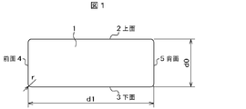
- FIG. 1 is a cross-sectional view showing an example of the shape of a general electronic device.
- 1 is an electronic device such as a camera or a measuring instrument
- 2 is an electronic device upper surface
- 3 is an electronic device lower surface
- 4 is an electronic device front surface
- 5 is an electronic device rear surface.
- the electronic device 1 such as a camera or a measuring instrument is generally installed in a case called a housing, particularly when installed outdoors, and thereafter, the electronic device is placed in the case. If so, the case will be described as a part of the electronic device.
- the height in the vertical direction of the electronic device front surface 4 and the electronic device back surface 5 is defined as d0
- the longitudinal lengths of the electronic device upper surface 2 and the electronic device lower surface are defined as d1
- a ratio d0 / d1 of d1 with respect to d0 Is in a relationship of 0.5.
- the ratio r / d0 of the housing height d0 is 0.042 with respect to the curvature radius r of the corner where the upper and lower surfaces of the housing and the front and rear surfaces are connected.
- the C D value according to the shape of the electronic apparatus 1 as 1.40 will be described in detail. This data is cited from Non-Patent Document 1.
- the electronic device 1 receives a drag that is pushed backward by the wind.
- the drag received by the electronic device 1 is D
- the density of the fluid air is ⁇
- the wind speed is V
- the drag coefficient is C D (Drag Coefficient)
- the area A that receives the wind pressure is reduced or the drag coefficient (hereinafter referred to as the CD value). Need to be small.
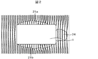
- FIG. 2 is a cross-sectional view showing the flow of wind as viewed from the right side of the electronic device shown in FIG.
- a plurality of straight lines are drawn in the vertical direction, and an arrow indicating the flow of wind comes out from here.
- the direction of this arrow indicates the direction of wind flow at this straight point, and the length of the arrow indicates the strength of the wind.
- reference numerals 21 a and 21 b denote backflow regions generated along the upper surface 2 and the lower surface 3 of the electronic device 1, respectively, and reference numeral 24 denotes a backflow region generated behind the electronic device 1.
- the wind When the wind hits the front of the electronic device 1, the wind collides with the front surface 4 of the electronic device and is dispersed in all directions.
- the dispersed winds flow toward the electronic device upper surface 2, the lower surface 3, and the left and right side surfaces, respectively.
- the wind toward the upper surface 2 is peeled off at the tip portion of the upper surface 2, and a backflow region 21a is generated.
- the wind toward the lower surface 3 is also peeled off at the tip portion of the lower surface 3, and a backflow region 21b is generated.
- a backflow region occurs on the left and right side surfaces.
- the wind that has passed through the upper and lower surfaces and the left and right side surfaces escapes behind the electronic device 1, the flow is separated behind the electronic device 1, and a large backflow region 24 is generated by winding a vortex.
- the electronic device 1 receives pressure drag that is pulled backward by these backflow regions.
- the present invention has been made to solve such problems, by reducing the C D value by reducing the pressure drag, cover the outdoor electronic device to reduce drag which the electronic device receives, it can withstand strong winds
- the purpose is to provide a structure.
- the cover structure of the electronic device of the present invention is provided on at least one side around the roof portion, the electronic device having a substantially cubic or substantially rectangular parallelepiped shape, a roof portion formed of at least one substantially square or substantially rectangular shape.
- a cover structure of an electronic device comprising a curved portion and a cover configured by a tip portion connected to the curved portion, the cover providing a predetermined gap between the electronic device, The tip portion is mounted so as to protrude outward from a corresponding end portion of any surface of the electronic device such that the tip portion faces the electronic device.
- the curved portion of the cover is provided around the entire roof portion, and the front end portion of the cover protrudes outward from each end portion of the surface of the electronic device. It is mounted.
- the cover structure of the electronic device is characterized in that the cover is mounted on a surface opposite to the surface of the electronic device on which the cover is mounted.
- the cover structure of the electronic device includes a substantially cubic or substantially rectangular parallelepiped electronic device, at least one substantially square or substantially rectangular roof portion, left and right side portions that are substantially square or substantially rectangular, and An electronic device comprising: a lower surface portion; a cover configured from a roof portion, the left and right side surface portions, and a curved portion connecting the left and right side surface portions and the lower surface portion, respectively.
- the cover structure is characterized in that the cover is mounted so as to cover the top, bottom, left and right of the electronic device.
- the distance (G) from the surface of the electronic device to which the cover is mounted to the roof portion is divided by the height (d0) of the electronic device.
- the cover is mounted on the electronic device so that the first ratio (gap ratio) takes a predetermined value from a range of about 0.25 to about 0.40. To do.
- the cover structure of the electronic device is characterized in that the first ratio (gap ratio) is about 0.30.
- the vertical distance (L) from the horizontal position of the surface of the electronic device on which the cover is mounted to the end of the tip of the cover is defined as the height of the electronic device (
- the second ratio (tip ratio) divided by d0) is used, and the cover is arranged so that the second ratio (tip ratio) takes a predetermined value from a range of about ⁇ 0.05 to about 0.40. It is mounted on equipment.
- the cover structure of the electronic device is characterized in that the second ratio (tip ratio) is 0.00.
- the cover further takes a predetermined value from a range of about 0.10 to about 0.40 when the second ratio is 0 or more. As described above, it is mounted on an electronic device.
- the roof portion is formed in a mountain shape with two or more substantially square or substantially rectangular shapes, and the gap from the surface of the electronic device on which the cover is mounted to the roof portion.
- a first ratio (gap ratio) obtained by dividing the distance (G) by the height (d0) of the electronic device, and the cover extends from the surface of the electronic device on which the cover is mounted to both ends of the roof portion.
- the distance of the gap from the surface of the electronic device to the center of the roof portion from the distance of the gap of the electronic device is such that the first ratio (gap ratio) is in the range of about 0.10 to about 0.40. It is attached to an electronic device so as to take a predetermined value from
- the cover structure of the electronic device is characterized in that the electronic device is a camera.
- a cover structure for an outdoor electronic device that can reduce the resistance that an electronic device installed outdoors or the like receives from the wind and can withstand the strong wind.
- FIG. 3 is a perspective view of a cover structure for an electronic apparatus according to an embodiment of the present invention.
- description of the same parts as those already described will be omitted.
- 8 is an upper cover attached to the electronic device 1
- 9a is a front curved portion of the upper cover 8
- 9b is a rear curved portion
- 10a is a front end portion
- 10b is a rear end portion
- 11a is a left side of the upper cover 8.
- a curved portion, 11b is a right curved portion of the upper cover 8
- 12a is a left end portion (not shown here) of the upper cover 8
- 12b is a right end portion of the upper cover 8.
- the upper cover 8 has a peripheral length longer than the peripheral length of the upper surface 2 of the electronic device 1, and covers the electronic device 1 slightly with a recessed surface facing downward with a predetermined gap therebetween. It is attached in the same way. Further, the periphery of the upper cover 8 is curved in a streamlined manner in the front / rear and left / right directions, and includes a front end portion 10a, a rear end portion 10b, a left end portion 12a, and a right end portion 12b. The entire periphery of the part is attached so as to protrude outward from all the side surfaces of the electronic device 1.
- connection / fixation structure between the electronic device 1 and the upper cover 8 is not particularly illustrated, but for example, the four corners of the electronic device 1 and the corresponding positions of the upper cover 8 are fixed with pins and fixed. There are various methods, and any method may be used. However, it is desirable to have a structure that does not inhibit the flow of wind as much as possible, such as reducing the ground contact area between the electronic device 1 and the upper cover 8.
- the wind When the wind blows from the front of the electronic device 1, the wind first collides with the front surface 4 of the electronic device 1 and is dispersed in all directions. Among these, the wind dispersed upward passes through the gap between the upper surface 2 of the electronic device 1 and the upper cover 8 and escapes to the rear of the electronic device 1. Further, when wind blows from the left side of the electronic device 1, the wind collides with the left side surface 6 of the electronic device 1 and is dispersed in all directions. Among these, the wind dispersed upward passes through the gap between the upper surface 2 of the electronic device 1 and the upper cover 8 and escapes to the right of the electronic device 1.
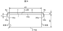
- FIGS. 4 is a cross-sectional view of the cover structure of the electronic apparatus shown in FIG. 3, which is an embodiment of the present invention, as viewed from the right side.
- reference numeral 18 a denotes a gap guiding area where the wind received on the front surface of the electronic apparatus 1 is guided to the gap between the electronic apparatus 1 and the upper cover 8, and 19 a denotes the wind flowing from the gap guiding area 18 a.
- the gap flow region 20 a is a gap discharge region where the wind flowing from the gap flow region 19 a is discharged to the rear of the electronic device 1.
- the wind When the wind blows from the front of the electronic device 1, the wind first collides with the front surface 4 of the electronic device 1 and is dispersed in all directions. Among these, the wind dispersed upward is guided from the gap guiding area 18 a to the gap between the electronic device 1 and the upper cover 8.
- the induced wind collides with the inside of the front curved portion 9a, changes its course, and flows toward the gap flow region 19a.
- the inside of the front curved portion 9a is curved in a streamline shape, it is possible to efficiently guide the wind to the gap flow region 19a.
- the wind that has flowed further flows rearward through the gap flow region 19a, collides with the inner side of the rear curved portion 9b, changes the course, and flows toward the gap discharge region 20a.
- the rear curved portion 9b is also curved in a streamline shape on the inner side, the wind can be efficiently guided to the gap discharge region 20a. Then, the wind is discharged from the gap discharge region 20a to the rear of the electronic device 1.
- the wind blown above the electronic device 1, particularly above the front end portion 10 a goes straight or collides with the front curved portion 9 a and flows to the rear of the electronic device 1 along the outside of the upper cover 8.
- FIG. 5 is a cross-sectional view of the cover structure of the electronic apparatus shown in FIG. 3, which is an embodiment of the present invention, as viewed from the front side.
- reference numeral 21 a denotes a gap guiding area in which the wind received on the left side surface of the electronic device 1 is guided in the gap between the electronic apparatus 1 and the upper cover 8, and 22 a denotes the wind flowing from the gap guiding area 21 a to the right.
- a flowing gap flow region 23 a is a gap discharge region where the wind flowing from the gap flow region 22 a is discharged to the right of the electronic device 1.
- the wind When the wind blows from the left side of the electronic device 1, the wind collides with the left side surface 6 of the electronic device 1 and is dispersed in all directions. Among these, the wind dispersed upward is guided from the gap guiding area 21 a to the gap between the electronic device 1 and the upper cover 8.
- the induced wind collides with the inside of the front curved portion 11a and flows toward the gap flow region 22a while changing the course.
- the inside of the front bending portion 11a is curved in a streamline shape, it is possible to efficiently guide the wind to the gap flow region 22a.
- the wind that has flowed further flows rearward through the gap flow region 22a, collides with the inside of the rear curved portion 11b, changes its path, and flows toward the gap discharge region 23a.
- the rear curved portion 11b is also curved in a streamline shape, the wind can be efficiently guided to the gap discharge region 23a. Then, the wind is discharged to the rear of the electronic device 1 from the gap discharge area 23a.
- the wind blown above the electronic device 1, particularly above the left end portion 12 a goes straight or collides with the front curved portion 11 a and flows toward the rear of the electronic device 1 along the outside of the upper cover 8.
- the cover 8 of the electronic device 1 can reduce the drag received by the electronic device 1 due to the wind while also serving as a sunshade.
- the cover is provided on the upper part of the electronic device 1, but it may be provided only on the lower part.
- FIG. 6 is a perspective view of an upper and lower cover structure of an electronic apparatus according to an embodiment of the present invention.
- reference numeral 13 denotes a lower cover attached to the electronic apparatus 1
- 14 a denotes a front curved portion of the lower cover 13
- 14 b denotes a rear curved portion of the lower cover 13
- 15 a denotes a front end portion of the lower cover 13
- 15 b denotes a lower cover 13.
- a rear end portion, 16a is a left curved portion of the lower cover 13
- 16b is a right curved portion of the lower cover
- 17a is a left end portion of the lower cover 13
- 17b is a right end portion of the lower cover 13.
- This embodiment differs from the first embodiment in that the electronic device 1 is provided with a lower cover 13 having the same shape as the upper cover 8 in the same relationship as the relationship of the upper cover 8 with respect to the electronic device 1. Since the configuration of the upper cover 8 and the flow of wind flowing through the gap between the electronic device 1 and the upper cover 8 are the same as those in the first embodiment, the description thereof is omitted.
- the connection / fixing structure between the electronic device 1 and the cover 8 may be the same as that of the first embodiment, and the description thereof is omitted.
- the lower cover 13 has a peripheral length longer than that of the lower surface 3 of the electronic device 1, and covers the electronic device 1 slightly with a recessed surface facing upward and a predetermined gap. It is attached in the same way. Further, the entire periphery of the curved portion including the front end portion 15a, the rear end portion 15b, the left end portion 17a, and the right end portion 17b of the lower cover 13 protrudes outward from each of all the side surfaces of the electronic device 1. It is attached in the state.
- the connection structure between the electronic device 1 and the lower cover 13 is the same as that of the upper cover described above.
- the wind dispersed upward is as described in the first embodiment.
- the wind dispersed downward passes through the gap between the lower surface 3 of the electronic device 1 and the lower cover 13 and escapes to the rear of the electronic device 1.
- the wind dispersed upward is as described in the first embodiment.
- the wind dispersed downward passes through the gap between the lower surface 3 of the electronic device 1 and the lower cover 13 and escapes to the right of the electronic device 1.
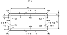
- FIG. 7 is a cross-sectional view of the upper and lower cover structure of the electronic apparatus shown in FIG. 6 which is an embodiment of the present invention, viewed from the right side.
- FIG. 8 is a cross-sectional view of the electronic device cover structure of this embodiment as viewed from the front side.
- reference numeral 18 b denotes a gap guiding area in which the wind received on the front surface of the electronic apparatus 1 is guided in the gap between the upper surface 2 of the electronic apparatus 1 and the upper cover 8, and 19 b denotes the wind flowing from the gap guiding area 18 b backward.
- a flowing gap flow region 20 b is a gap discharge region where the wind flowing from the gap flow region 19 b is discharged to the rear of the electronic device 1.
- the relationship between the lower surface 3 and the lower cover 13 of the electronic device 1 is the same as the relationship between the upper surface 2 and the upper cover 8.
- the wind When the wind blows from the front of the electronic device 1, the wind first collides with the front surface 4 of the electronic device 1 and is dispersed in all directions. Among these, the wind dispersed upward is as described in the first embodiment. The wind dispersed downward is guided to the gap between the electronic device 1 and the lower cover 13 from the gap guiding area 18b. The induced wind collides with the inside of the front curved portion 14a, changes its course, and flows toward the gap flow region 19b. The wind that has flowed further flows rearward through the gap flow region 19b, collides with the inside of the rear curved portion 14b, changes the course, and flows toward the gap discharge region 20b. Then, the wind is discharged to the rear of the electronic device 1 from the gap discharge region 20b. At this time as well, as in the case of the upper cover 8, the inside of the front curved portion 14a and the rear curved portion 14b is rounded and has a streamline shape, so that wind can be efficiently guided to the gap flow region 19a. it can.
- the wind blown below the electronic device 1 goes straight or collides with the front curved portion 14 a and flows to the rear of the electronic device 1 along the outside of the lower cover 13.
- FIG. 8 is a cross-sectional view of the upper and lower cover structure of the electronic apparatus shown in FIG. 6 which is an embodiment of the present invention, as viewed from the front side. The description of the same parts as those described in FIGS. 1 to 7 is omitted.
- reference numeral 21b denotes a gap guiding region where the wind received on the left side surface of the electronic device 1 is guided to the gap between the electronic device 1 and the lower cover 13, and 22b denotes the wind flowing from the gap guiding region 21b to the right.
- a flowing gap flow area 23 b is a gap discharge area where the wind flowing from the gap flow area 22 b is discharged to the right of the electronic device 1.
- the wind collides with the left side surface 6 of the electronic device 1 and is dispersed in all directions.
- the wind dispersed upward is as described in the first embodiment.
- the wind dispersed downward is guided to the gap between the electronic device 1 and the lower cover 13 from the gap guiding area 21b.
- the induced wind collides with the inside of the left curved portion 16a, changes its course, and flows toward the gap flow region 22b.
- the wind that has flowed further flows backward through the gap flow region 22b, collides with the inside of the right-hand curved portion 16b, and flows toward the gap discharge region 23b while changing the course.
- the left curved portion 16a and the right curved portion 16b are curved in a streamline shape on the inner side, so that the wind can be efficiently guided to the gap discharge region 23b. Can do. Then, the wind is discharged to the rear of the electronic device 1 from the gap discharge area 23b.
- the wind blown below the electronic device 1, particularly below the left end portion 17 a goes straight or collides with the left curved portion 16 a and flows to the right of the electronic device 1 along the outside of the lower cover 13. Go.
- FIG. 9 is a cross-sectional view showing an example of the flow of wind as seen from the right side of the upper and lower cover structure of the electronic device shown in FIG. 6 which is an embodiment of the present invention.
- reference numerals 26a and 26b denote backflow areas generated along the outer surfaces of the upper cover 8 and the lower cover 13, 27a and b denote divided backflow areas, and 28 denotes a backflow generated spirally behind the electronic device 1, respectively. It is an area.
- the wind When wind is blown from the front of the electronic device 1, the wind collides with the front surface 4 of the electronic device and is dispersed in all directions.
- the dispersed wind flows from the front surface 4 of the electronic device in all directions, and the gap between the upper surface 2 of the electronic device 2 and the upper cover 8, the gap between the lower surface 3 and the lower cover 13, and the left and right side surfaces 6, It flows backward along 7.
- the wind that flows in the gap between the upper surface 2 of the electronic device 1 and the upper cover 8 and the wind that flows in the gap between the lower surface 3 of the electronic device 1 and the lower cover 13 are the gap induction regions 18a, 18b, the gap flow region 19a, It is discharged to the rear of the electronic device 1 through b and the gap discharge areas 20a and 20b.
- a large backflow area behind the electronic device 1 generated by the wind that flows along the outer surfaces of the upper cover 8 and the lower cover 13 passes through the gap between the upper surface 2 of the electronic device 2 and the upper cover 8 and is discharged from the gap discharge region 20a. And the air discharged from the gap discharge region 20b through the gap between the lower surface 3 and the lower cover 13 is divided into the reverse flow regions 27a and 27b and the reverse flow region 28, and the reverse flow region becomes smaller.
- the acceleration of the wind flow outside the upper cover 8 and the outside of the lower cover 13 is suppressed, so that the backflow regions 26a and 26b are reduced and the pressure drag can be reduced. And the CD value can be reduced.
- the distances between the upper and lower surfaces of the electronic apparatus and the upper and lower covers varies depending on the vertical distance from the horizontal position of the upper and lower surfaces of the electronic device to the tip of the upper and lower covers.
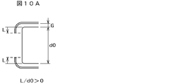
- the definitions of the tip ratio L / d0 and the gap ratio G / d0 of the upper and lower cover structures of the electronic apparatus according to the present invention will be described with reference to FIGS. 10A, 10B, and 10C.
- the tip position L is a vertical distance from the horizontal position of the upper surface 2 of the electronic device 1 to the front end portion 10a or the rear end portion 10b of the upper cover 8 (from the horizontal position of the lower surface 3 to the front end portion 15a or the rear of the lower cover 13). The same applies to the distance in the vertical direction to the end 15b.
- the tip ratio L / d0 represents the ratio of the tip position L to the height d0 of the electronic device 1, and is calculated by dividing the tip position L by the height d0.
- the center direction of the electronic device 1 is a positive direction, and the outer direction of the electronic device 1 is a negative direction.
- G represents the distance from the upper surface 2 of the electronic device 1 to the upper cover 8 (the same applies to the distance from the lower surface 3 to the lower cover 13), that is, the gap distance.
- G / d0 represents the ratio of the gap G to the height d0 of the electronic device 1, and is calculated by dividing the gap G by the height d0.
- the tip ratio L / d0 and the gap ratio G / d0 are the same in the relationship between the lower surface 3 and the lower cover 13.
- the optimum ranges and optimum values of L / d0 and G / d0 will be described with reference to FIGS. 11, 12A, 12B, 13A, 13B, and 13C under this definition.
- FIG. 11 the relationship between the tip ratio (L / d0) and the drag coefficient of each value of the gap ratio of the upper and lower cover structure of an electronic device which is an embodiment (G / d0) of the present invention (C D value)
- C D value It is a graph showing, showing the experimental result of the relationship between L / d0 and C D value for each value of G / d0 in the graph.
- C D value is referenced to 0.9 (conventional ratio of about 35% decrease), C D value is described ranges and optimal values of G / d0 and L / d0 to be 0.9 or less.
- C D value of the electronic apparatus 1 of the absence of the upper and lower covers 8,13 is 1.40.
- the graph of FIG. 12A and the graph of FIG. 12B are the gap ratio (G / d0) and the drag coefficient for each value of the tip ratio (L / d0) of the upper and lower cover structures of the electronic apparatus which is an embodiment of the present invention.
- C D value is referenced to 0.75 (conventional fell about 46%), C D value is described ranges and optimal values of G / d0 and L / d0 to be 0.75 or less.
- the electronic device 1 is a camera
- a glass surface is provided on the front surface 4 and light is taken in through the glass surface. Therefore, if the value of L / d0 is too large, The front end portion 10a and the front end portion 15a of the lower cover 13 are reflected in the angle of view of the camera. Therefore, in this case, it is desirable to set L / d0 to a value that is not too large (for example, a range of L / d0 ⁇ 0.40).
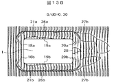
- FIG. 13A, FIG. 13B, and FIG. 13C show the flow of wind as viewed from the right side for each value of the gap ratio (G / d0) in another embodiment of the upper and lower cover structure of the electronic device that is one embodiment of the present invention.
- G / d0 0.10
- Each configuration here and the basic wind flow are the same as in the case shown in FIG.
- the backflow regions 26 a and 26 b are largely generated along the outer surfaces of the upper and lower covers 8 and 13 due to the wind flowing along the outer surfaces of the upper and lower covers 8 and 13. That is, the backflow region generated in the gap between the electronic device 1 and the upper and lower covers 8 and 13 is small, but the backflow regions 26a and 26b generated along the outer surfaces of the upper and lower covers 8 and 13 are increased.
- the backflow regions 26 a and 26 b are slightly generated along the outer surfaces of the upper and lower covers 8 and 13 due to the wind flowing along the outer surfaces of the upper and lower covers 8 and 13. That is, if the gap between the electronic device 1 and the upper and lower covers 8 and 13 is balanced, the backflow region generated in the gap between the electronic device 1 and the upper and lower covers 8 and 13 also extends along the outer surface of the upper and lower covers 8 and 13.
- the backflow regions 26a and 26b generated in this way are also small, and the backflow regions inside and outside the cover are reduced in total.
- the backflow regions 26 a and 26 b are slightly generated along the outer surfaces of the upper and lower covers 8 and 13 due to the wind flowing along the outer surfaces of the upper and lower covers 8 and 13. That is, although the backflow regions 26a and 26b generated along the outer surfaces of the upper and lower covers 8 and 13 are small, the backflow region generated in the gap between the electronic device 1 and the upper and lower covers 8 and 13 is increased.
- narrowing the gap between the electronic device and the cover and increasing the length of the tip of the cover means reducing the amount of wind flowing into the gap and increasing the amount of wind flowing outside the cover. is there.
- widening the gap between the electronic device and the cover and shortening the length of the tip of the cover are to increase the amount of wind flowing into the gap and reduce the amount of wind flowing outside the cover. .
- the amount of wind that flows into the gap and the amount of wind that flows to the outside of the cover are not biased to either, but balance is important, and the length of the gap between the electronic device and the cover and the cover It is important to set the length of the tip.
- L / d0 the value of L / d0 is fixed to 0.14.
- the electronic device since the drag received by the electronic device is reduced, the electronic device is less likely to be blown by the wind, and the normal operation state of the electronic device can be continued.
- the durability of the electronic device itself is improved by reducing the drag that the electronic device receives. Furthermore, since the drag received by the electronic device is reduced, the load on the base such as a pole to which the electronic device is fixed is reduced, and the durability of the base as well as the electronic device is improved.
- the electronic device when it is a camera, it is attached to a device called a pan head that rotates in a horizontal direction (pan) and a vertical direction (tilt), and may be picked up by freely moving the imaging direction.
- a pan head that rotates in a horizontal direction (pan) and a vertical direction (tilt), and may be picked up by freely moving the imaging direction.
- the drag received by the camera is large at this time, a large amount of power is required for the turning operation, and a large amount of power consumption is required.
- the cover structure of the present invention is applied, the drag received by the electronic device is reduced, so that the drag received by the camera is reduced, and a small amount of power is required during the turning operation, thereby saving power.
- the pan head since the power of the pan head can be reduced, the pan head can be reduced in size, and the cost of the entire camera and pan head device can be reduced. Further, the angle of view is less likely to be shifted by the camera being blown by the wind, and a good imaging operation can
- FIG. 14 is a perspective view of a mountain-shaped cover structure for an electronic apparatus according to an embodiment of the present invention.
- the shape of the upper cover 8 ′ is different from that of the first embodiment, and in this embodiment, the upper cover 8 ′ has a mountain shape from the left curved portion 11a ′ and the right curved portion 11b ′ toward the center.
- “′” is added to the portion corresponding to the configuration of the upper cover 8 of the first embodiment.
- the configuration of the upper cover 8 ′ and the flow of the wind flowing through the gap between the electronic device 1 and the upper cover 8 are substantially the same as those in the first embodiment, and therefore will be omitted.
- the connection structure between the electronic device 1 and the cover 8 may be the same as that of the first embodiment, and the description thereof is omitted.
- G / d0 may be set to the height of the end and center of the summit portions of the right and left within a range of values C D value is reduced in the FIGS. 12A and 12B.
- the upper cover 8 ' has a mountain shape, the snow, dust, and the like that have fallen on the upper cover 8' slide down. As a result, it is possible to simultaneously reduce both the drag received by the electronic device due to the wind and the load received by the accumulation of snow, dust, and the like.
- FIG. 15 is a perspective view of a mountain-shaped upper and lower cover structure of an electronic apparatus according to an embodiment of the present invention.
- the present embodiment is different from the second embodiment in that the lower cover 13 'and the lower cover 13' are mountain-shaped, and the lower cover 13 'having the same shape as the upper cover 8' is different from the third embodiment in that the electronic device 1 It differs in that it is provided in the same relationship as that of the upper cover 8 '.
- “′” is added to portions corresponding to the configurations of the upper and lower covers 8 and 13 of the second embodiment.
- the configuration of the lower cover 13 ′ and the flow of the air flowing through the gap between the electronic device 1 and the lower cover 13 ′ are substantially the same as those in the second embodiment, and will be omitted.
- the connection structure between the electronic device 1 and the cover 8 may be the same as that of the first embodiment, and the description thereof is omitted.
- the lower cover 13 ′ has the same mountain structure as the upper cover 8 ′, but may have a structure other than the mountain shape as in the second embodiment.
- the present embodiment as in the third embodiment, it is possible to simultaneously reduce both the drag received by the electronic device due to the wind and the load received by the accumulation of snow, dust, etc., and the presence of the lower cover provides the electronic device. Can be further reduced as compared with the third embodiment.
- FIG. 16 is a perspective view of an electronic device surrounding cover structure (square tube shape) according to an embodiment of the present invention
- FIG. 17 is a perspective view of an electronic device surrounding cover structure (cylindrical shape) according to an embodiment of the present invention. It is.
- reference numeral 29 denotes an enveloping cover that covers the upper, lower, left, and right sides of the electronic device 1
- 30 a is a front bending portion of the enclosing cover
- 30 b is a rear bending portion of the enclosing cover
- 31 a is a front of the surrounding cover 29.
- the electronic device 1 is provided with an enveloping cover that covers four directions, up, down, left, and right.
- the connection structure between the electronic device 1 and the cover 8 may be the same structure as that of the first embodiment or an applied structure.
- 16 and 17 the shape of the surrounding cover is different between the square tube shape and the cylindrical shape, but the flow of the wind in the basic gap is the same, and the flow of the wind outside the surrounding cover is slightly different. .
- the wind flow in the cross section obtained by horizontally cutting the electronic device 1 and the surrounding cover 29 of the present embodiment and the wind flow in the cross section cut perpendicularly in the front-rear direction are substantially the same as the wind flow in FIG.
- the values of the tip ratio L / d0 and the gap ratio G / d0 are set in the same manner as in the second embodiment shown in FIGS. 11, 12A, and 12B. in, covering the C D value can be greatly reduced as compared to when there is no, it is possible to significantly reduce the drag experienced by the turn electronics.
- the cover is covered not only in the vertical direction but also in the horizontal direction, so that when the wind blows from the front and rear direction, for example, in a train or a car, the electrons are more effectively applied.
- the drag received by the device can be reduced.
- the upper surface of the surrounding cover 29 may have a mountain-shaped structure as in the fourth embodiment, and in this case, the value of the gap ratio G / d0 is set in an arbitrary range where the effect is exerted as in the third embodiment. Just do it. Thereby, both the drag received by the electronic device due to the wind and the load received by the accumulation of snow, dust, etc., as in the third embodiment can be reduced at the same time.
- the gap ratio and the tip ratio were determined based on the height of the electronic device, but the reference is not limited to the height of the electronic device. It goes without saying that the ratio may be obtained based on the electronic device or any other part.
- the present invention is not limited to the above-described embodiments as they are, and can be embodied by modifying the components without departing from the scope of the invention in the implementation stage.
- various inventions can be formed by appropriately combining a plurality of constituent elements disclosed in the above embodiments. For example, some components may be deleted from all the components shown in each embodiment. Furthermore, you may combine suitably the component covering different embodiment.
Landscapes
- Physics & Mathematics (AREA)
- General Physics & Mathematics (AREA)
- Engineering & Computer Science (AREA)
- Multimedia (AREA)
- Signal Processing (AREA)
- Casings For Electric Apparatus (AREA)
- Studio Devices (AREA)
Abstract
強風に耐え得る屋外電子機器のカバー構造を提供することを目的とする。 上カバー8は、電子機器1に対して上方に所定の間隙を設けてやや覆いかぶさる様にして取り付けられる。さらに、上カバー8の前方端部10a,bおよび左右端部12a,bを含む上カバー8の縁全周は、電子機器1の全ての側面よりも外側に突出して取り付けられる。電子機器1の前方から風が吹き付けると、まず風は電子機器1の前面4に衝突して四方八方に分散される。この内、上方に分散された風は電子機器1と上カバー8との間隙を通って電子機器1の後方へと抜けていく。また、電子機器1の左方から風が吹き付けると、風は電子機器1の左側面6に衝突して四方八方に分散される。この内、上方に分散された風は電子機器1と上カバー8の間を通って電子機器1の右方へと抜けていく。
Description
本発明は、屋外等に設置される電子機器のカバー構造に関するものである。
従来、屋外に電子機器を設置する場合が増加しているが、風に晒されることで安定的な動作の確保が難しい。以下に、図を用いて従来の屋外に設置される電子機器の様子について説明する。
図1は一般的な電子機器の形状の一例を示す断面図である。図1において、1はカメラや測定器等の電子機器、2は電子機器上面、3は電子機器下面、4は電子機器前面、5は電子機器背面である。カメラや測定器等の電子機器1は、特に屋外等に設置される場合は、ハウジングと呼ばれる様なケースに入れて設置されるのが一般的であり、以降では、電子機器がケースに入っている場合はケースも電子機器の一部として説明する。
ここで、電子機器前面4および電子機器背面5の上下方向の高さをd0とし、電子機器上面2および電子機器下面の前後方向の長さをd1とし、d0に対してd1の比率d0/d1が0.5の関係にあることとする。また、ハウジング上下面と前背面が接続した角の曲率半径rに対してハウジング高さd0の比率r/d0が0.042の関係にあることとする。また、この電子機器1の形状に係るCD値を1.40として、以下詳細に説明する。なお、このデータは、非特許文献1から引用したものである。
まず、第1に、電子機器1に前方から風が吹きつけられると、風は電子機器前面4に衝突し四方八方に分散される。分散された風はそれぞれ、電子機器上面2、下面3および左右の側面に沿って後方へ流れる。その際、電子機器1は風の流れによって、空気が有する流体粘性による摩擦抗力が電子機器1の表面に働き、風と一緒に後方に押し流される力を受ける。
第2に、風が電子機器1の前面に衝突すると、電子機器1の前方では風の流れが遅くなることで空気の圧力が周囲より上昇する(圧力上昇)。この圧力上昇により、電子機器1は上流から下流へ向かって押付力を受ける。さらに、風が電子機器1の後方に流れ去る際、電子機器1の後方では、風の流線が物体から離れて(剥離して)、いわゆる剥離領域(流れが逆になることから逆流領域とも言う)が発生することで空気の圧力が周囲より降下する(圧力降下)。この圧力降下により、電子機器1は後方へ引っ張られる吸引力を受ける。これら電子機器1前方の圧力上昇と後方の圧力降下が組み合わさり、圧力抗力として電子機器1に作用することにより、電子機器1は風の流れと一緒に後方へ押し流される力を受ける。
そして、これら摩擦抗力と圧力抗力が合わさることで、電子機器1は風によって後方へと押し流される抗力を受ける。
ここで、電子機器1が受ける抗力をD、流体である空気の密度をρ、風速をV、抗力係数をCD(Drag Coefficient)、風の流れに垂直な電子機器1の面(上記の場合は前面4)の面積をAとすると、電子機器1が受ける抗力は次式で一般的に求めることができる。
D=CD×A×ρ/2×V2・・・(式1)
D=CD×A×ρ/2×V2・・・(式1)
この式1から、電子機器1に吹き付けられる風速に関係なく電子機器1が受ける抗力Dを小さくするためには、風圧を受ける面積Aを小さくするか、抗力係数(以下、CD値とする)を小さくする必要がある。
図2は、図1に示す電子機器における右側面側から見た風の流れを示す断面図である。この断面図には、縦方向に複数の直線が引いてあり、ここから風の流れを示す矢印が出ている。この矢印の向きはこの直線の地点における風の流れる方向を示しており、矢印の長さは風の強さを示している。この条件は、後に説明する図9、図13A、図13B、および図13Cにおいても同様とする。図2において、21a,bはそれぞれ電子機器1の上面2および下面3に沿って発生する逆流領域、24は電子機器1の後方に発生する逆流領域である。
電子機器1の前方に風が当ると、風は電子機器前面4に衝突し四方八方に分散される。分散された風はそれぞれ、電子機器上面2、下面3および左右の側面方向へと流れる。上面2に向かった風は、上面2の先端部分で剥離し、逆流領域21aが発生する。同様に、下面3に向かった風も、下面3の先端部分で剥離し、逆流領域21bが発生する。同様に左右の側面でも逆流領域が発生する。そして、上下面及び左右側面を通過した風は電子機器1の後方に抜け、電子機器1の後方で流れが剥離し、渦を巻くことで大きな逆流領域24が発生する。これらの逆流領域により電子機器1は後方へ引っ張られる圧力抗力を受ける。
なお、屋外等に設置される電子機器、特にカメラ装置において、日除けカバーがハウジングに固定され、ハウジングの前面ガラスから入射する光を適度に遮る構造が用いられている(特許文献1参照)。
上記の様な電子機器の場合、屋外に設置される際には、常に風に晒されることとなるため、日光等の光や雨、雪等だけでなく、風の影響も受けることになる。近年、電子機器に強い風が吹きつけられると、煽られたり回転したり揺れたりして正常な運用ができなくなることがあり、特に、台風や海沿いまたは陸地の竜巻、空港等のダウンバースト等による強風下においての屋外機器の耐風圧に対する要求が高まっている。特に電子機器がカメラである場合は、画角がずれる等、適切な映像を取得できないといった弊害がある。また、ポールの上部に取り付けられたり不安定な場所に設置されたりしている場合には、固定部分の破損等といった弊害もある。従来の電子機器のカバー構造では、風圧対策に重点を置いて検討されておらず、上記要求される耐風圧性能を満たすことができなかった。
本発明はこの様な問題を解決するためになされたもので、圧力抗力を低減してCD値を小さくすることで、電子機器が受ける抗力を低減し、強風に耐え得る屋外電子機器のカバー構造を提供することを目的とする。
本発明の電子機器のカバー構造は、略立方体または略直方体形状の電子機器と、少なくとも1つの略正方形または略長方形状で構成される屋根部と、前記屋根部の周囲の少なくとも1辺に設けられた湾曲部と、該湾曲部に接続される先端部とから構成されるカバーと、を備える電子機器のカバー構造であって、前記カバーは、前記電子機器との間に所定の間隙を設け、前記先端部が前記電子機器側を向く様に、前記先端部が前記電子機器のいずれかの面の対応する端部より外側に突出させて装着されることを特徴とする。
また、上記電子機器のカバー構造は、前記カバーの湾曲部は、前記屋根部の全周囲に設けられ、前記カバーは、前記先端部が前記電子機器の面の各端部より外側に突出させて装着されることを特徴とする。
また、上記電子機器のカバー構造は、前記カバーは、前記電子機器の前記カバーが装着された面と逆側の面にも装着されることを特徴とする。
また、上記電子機器のカバー構造は、略立方体または略直方体形状の電子機器と、少なくとも1つの略正方形または略長方形状で構成される屋根部と、略正方形または略長方形状の左右の側面部および下面部と、前記屋根部と前記左右の側面部および前記左右の側面部と前記下面部とをそれぞれ接続する湾曲部とから構成されるカバーまたは筒状に構成されるカバーと、を備える電子機器のカバー構造であって、前記カバーは、前記電子機器の上下左右を覆う様に装着されることを特徴とする。
また、上記電子機器のカバー構造は、前記電子機器の前記カバーが装着された面から前記屋根部までの前記間隙の距離(G)を前記電子機器の高さ(d0)で除算した第1の比率(間隙比率)とし、前記カバーは、前記第1の比率(間隙比率)が約0.25~約0.40の範囲から所定の値をとる様に電子機器に装着されることを特徴とする。
また、上記電子機器のカバー構造は、前記第1の比率(間隙比率)が約0.30であることを特徴とする。
また、上記電子機器のカバー構造は、前記電子機器の前記カバーが装着された面の水平位置から前記カバーの前記先端部の末端までの垂直方向の距離(L)を前記電子機器の高さ(d0)で除算した第2の比率(先端比率)とし、前記カバーは、前記第2の比率(先端比率)が約-0.05~約0.40の範囲から所定の値をとる様に電子機器に装着されることを特徴とする。
また、上記電子機器のカバー構造は、前記第2の比率(先端比率)が0.00であることを特徴とする。
また、上記電子機器のカバー構造は、前記カバーは、さらに、前記第2の比率が0以上のときには、前記第1の比率が約0.10~約0.40の範囲から所定の値をとる様に電子機器に装着されることを特徴とする。
また、上記電子機器のカバー構造は、前記屋根部は、2以上の略正方形または略長方形状で山型に構成され、前記電子機器の前記カバーが装着された面から前記屋根部までの前記間隙の距離(G)を前記電子機器の高さ(d0)で除算した第1の比率(間隙比率)とし、前記カバーは、前記電子機器の前記カバーが装着された面から前記屋根部の両端までの間隙の距離から前記電子機器の前記カバーが装着された面から前記屋根部の中央までの間隙の距離が、前記第1の比率(間隙比率)が約0.10~約0.40の範囲からそれぞれ所定の値をとる様に電子機器に装着されることを特徴とする
また、上記電子機器のカバー構造は、前記電子機器は、カメラであることを特徴とする。
したがって、本発明によれば、屋外等に設置される電子機器が風から受ける抗力を低減し、強風に耐え得る屋外電子機器のカバー構造を提供することができる。
以下、図面を参照して本発明の実施の形態について詳細に説明する。まず、図3、図4および図5を用いて、電子機器に上カバーが設けられた実施例について説明する。図3は本発明の一実施例である電子機器のカバー構造の斜視図である。以降、既に説明した部分と同じ部分については説明を省略する。
図3において、8は電子機器1に取り付ける上カバー、9aは上カバー8の前方湾曲部、9bは後方湾曲部、10aは前方端部、10bは後方端部、11aは上カバー8の左方湾曲部、11bは上カバー8の右方湾曲部、12aは上カバー8の左方端部(ここでは図示せず)、12bは上カバー8の右方端部である。
上カバー8は、縁の周囲の長さが電子機器1の上面2の周囲の長さより長く、電子機器1に対して、窪み面を下にして、上方に所定の間隙を設けてやや覆い被さる様にして取り付けられる。さらに、上カバー8の周囲はそれぞれ前後左右方向に流線形上に湾曲しており、上カバー8の前方端部10a,後方端部10bおよび左方端部12a,右方端部12bを含む湾曲部の縁全周は、電子機器1の全ての側面よりも外側に突出して取り付けられる。
なお、ここでは電子機器1と上カバー8の接続・固定構造については特に図示していないが、例えば電子機器1の四つ角とそれに対応する上カバー8の位置にピンで止めて接続・固定する等、様々な方法があり、どの様な方法が用いられても良い。ただし、電子機器1と上カバー8の接地面積を小さくする等、できるだけ風の流れを阻害しない構造とするのが望ましい。
電子機器1の前方から風が吹き付けると、まず風は電子機器1の前面4に衝突して四方八方に分散される。この内、上方に分散された風は電子機器1の上面2と上カバー8との間隙を通って電子機器1の後方へと抜けていく。また、電子機器1の左方から風が吹き付けると、風は電子機器1の左側面6に衝突して四方八方に分散される。この内、上方に分散された風は電子機器1の上面2と上カバー8との間隙を通って電子機器1の右方へと抜けていく。
一方、下方に分散された風は電子機器1の下方へと流れ、下面3に沿って電子機器1の後方へと抜けていく。
ここで、図4および図5を用いて、図3に示す本実施例における風の流れについて詳細に説明する。図4は本発明の一実施例である図3に示す電子機器のカバー構造を右側面側から見た断面図である。
図4において、18aは電子機器1の前面に受けた風が電子機器1と上カバー8との間隙へと誘導される間隙誘導領域、19aは間隙誘導領域18aから流れてきた風が後方へ流れる間隙流動領域、20aは間隙流動領域19aから流れてきた風が電子機器1の後方へ排出される間隙排出領域である。
電子機器1の前方から風が吹き付けると、まず風は電子機器1の前面4に衝突して四方八方に分散される。この内、上方に分散された風は、間隙誘導領域18aから電子機器1と上カバー8の間隙に誘導される。誘導された風は前方湾曲部9aの内側に衝突し、進路を変えて間隙流動領域19aに向かって流れる。このとき、前方湾曲部9aの内側は流線形状に湾曲しているため、間隙流動領域19aへと効率良く風を誘導することができる。流れた風は、間隙流動領域19aを通ってさらに後方へと流れ、後方湾曲部9bの内側に衝突し、進路を変えて間隙排出領域20aに向かって流れる。このとき、後方湾曲部9bもまた、内側が流線形状に湾曲しているため、間隙排出領域20aへと効率良く風を誘導することができる。そして、風は間隙排出領域20aから電子機器1の後方へ排出される。
また、電子機器1の上部、特に前方端部10aより上に吹き付けた風は直進または前方湾曲部9aに衝突し、上カバー8の外側に沿って電子機器1の後方へと流れていく。
図5は本発明の一実施例である図3に示す電子機器のカバー構造を前面側から見た断面図である。図5において、21aは電子機器1の左側面に受けた風が電子機器1と上カバー8との間隙に誘導される間隙誘導領域、22aは間隙誘導領域21aから流れてきた風が右方へ流れる間隙流動領域、23aは間隙流動領域22aから流れてきた風が電子機器1の右方へ排出される間隙排出領域である。
電子機器1の左方から風が吹き付けると、風は電子機器1の左側面6に衝突して四方八方に分散される。この内、上方に分散された風は、間隙誘導領域21aから電子機器1と上カバー8の間隙に誘導される。誘導された風は前方湾曲部11aの内側に衝突し、進路を変えて間隙流動領域22aに向かって流れる。このとき、前方湾曲部11aの内側は流線形状に湾曲しているため、間隙流動領域22aへと効率良く風を誘導することができる。流れた風は、間隙流動領域22aを通ってさらに後方へと流れ、後方湾曲部11bの内側に衝突し、進路を変えて間隙排出領域23aに向かって流れる。このとき、後方湾曲部11bもまた、内側が流線形状に湾曲しているため間隙排出領域23aへと効率良く風を誘導することができる。そして、風は間隙排出領域23aから電子機器1の後方へ排出される。
また、電子機器1の上部、特に左方端部12aより上に吹き付けた風は直進または前方湾曲部11aに衝突し、上カバー8の外側に沿って電子機器1の後方へと流れていく。
上記実施例によれば、電子機器1のカバー8は、日除けの役割も果たしつつ、風により電子機器1が受ける抗力を低減することができる。
なお、本実施例では電子機器1の上部にカバーを設ける構造としたが、下部のみに設ける構造としても良い。
次に、図6、図7、図8および図9を用いて、電子機器に上カバーおよび下カバーが設けられた実施例について、その構造および基本的な風の流れを説明する。図6は本発明の一実施例である電子機器の上下カバー構造の斜視図である。
図6において、13は電子機器1に取り付ける下カバー、14aは下カバー13の前方湾曲部、14bは下カバー13の後方湾曲部、15aは下カバー13の前方端部、15bは下カバー13の後方端部、16aは下カバー13の左方湾曲部、16bは下カバー13の右方湾曲部、17aは下カバー13の左方端部、17bは下カバー13の右方端部である。
本実施例は、上記した実施例1と比べて、電子機器1に、上カバー8と同形状の下カバー13を、電子機器1に対する上カバー8の関係と同じ関係で設けた点で異なる。上カバー8の構成と、電子機器1と上カバー8との間隙に流れる風の流れについては実施例1と同じなので説明は省略する。また、電子機器1とカバー8との接続・固定構造についても実施例1と同様の構造をとれば良いため説明は省略する。
下カバー13は、縁の周囲の長さが電子機器1の下面3の周囲の長さより長く、電子機器1に対して、窪み面を上にして、下方に所定の間隙を設けてやや覆い被さる様にして取り付けられる。さらに、下カバー13の前方端部15a,後方端部15bおよび左方端部17a,右方端部17bを含む湾曲部の縁全周は、電子機器1の全ての側面それぞれよりも外側に突出した状態で取り付けられる。電子機器1と下カバー13の接続構造については上記した上カバーの場合と同様の構造が用いられる。
電子機器1の前方から風が吹き付けると、まず風は電子機器1の前面4に衝突して四方八方に分散される。この内、上方に分散された風については、実施例1にて述べた通りである。一方、下方に分散された風は、電子機器1の下面3と下カバー13との間隙を通って電子機器1の後方へと抜けていく。また、電子機器1の左方から風が吹き付けると、風は電子機器1の左側面6に衝突して四方八方に分散される。この内、上方に分散された風については、実施例1にて述べた通りである。下方に分散された風は電子機器1の下面3と下カバー13との間隙を通って電子機器1の右方へと抜けていく。
図7は本発明の一実施例である図6に示す電子機器の上下カバー構造を右側面側から見た断面図である。図8は本実施例の電子機器のカバー構造の前面側から見た断面図である。
図7において、18bは電子機器1前面に受けた風が電子機器1の上面2と上カバー8との間隙に誘導される間隙誘導領域、19bは間隙誘導領域18bから流れてきた風が後方へ流れる間隙流動領域、20bは間隙流動領域19bから流れてきた風が電子機器1の後方へ排出される間隙排出領域である。なお、電子機器1の下面3および下カバー13との関係についても上面2と上カバー8との関係と同様である。
電子機器1の前方から風が吹き付けると、まず風は電子機器1の前面4に衝突して四方八方に分散される。この内、上方に分散された風については、実施例1で述べた通りである。下方に分散された風については、間隙誘導領域18bから電子機器1と下カバー13の間隙に誘導される。誘導された風は前方湾曲部14aの内側に衝突し、進路を変えて間隙流動領域19bに向かって流れる。流れた風は、間隙流動領域19bを通ってさらに後方へと流れ、後方湾曲部14bの内側に衝突し、進路を変えて間隙排出領域20bに向かって流れる。そして、風は間隙排出領域20bから電子機器1の後方へ排出される。このときも、上カバー8の場合と同様に、前方湾曲部14a,後方湾曲部14bの内側は丸みを帯びて流線形状であるため、間隙流動領域19aへと効率良く風を誘導することができる。
また、電子機器1の下方、特に前方端部15aより下に吹き付けた風は直進または前方湾曲部14aに衝突し、下カバー13の外側に沿って電子機器1の後方へと流れていく。
図8は本発明の一実施例である図6に示す電子機器の上下カバー構造を前面側から見た断面図である。図1~7において説明した部分と同じ部分については説明を省略する。図8において、21bは電子機器1の左側面に受けた風が電子機器1と下カバー13との間隙に誘導される間隙誘導領域、22bは間隙誘導領域21bから流れてきた風が右方へ流れる間隙流動領域、23bは間隙流動領域22bから流れてきた風が電子機器1の右方へ排出される間隙排出領域である。
電子機器1の左方から風が吹き付けると、風は電子機器1の左側面6に衝突して四方八方に分散される。この内、上方に分散された風については実施例1で述べた通りである。下方に分散された風は、間隙誘導領域21bから電子機器1と下カバー13の間隙に誘導される。誘導された風は左方湾曲部16aの内側に衝突し、進路を変えて間隙流動領域22bに向かって流れる。流れた風は、間隙流動領域22bを通ってさらに後方へと流れ、右方湾曲部16bの内側に衝突し、進路を変えて間隙排出領域23bに向かって流れる。このときも、上カバー8の場合と同様に左方湾曲部16a,右方湾曲部16bは、内側が流線形状に湾曲しているため、間隙排出領域23bへと効率良く風を誘導することができる。そして、風は間隙排出領域23bから電子機器1の後方へ排出される。
また、電子機器1の下部、特に左方端部17aより下に吹き付けた風は直進または左方湾曲部16aに衝突し、下カバー13の外側に沿って電子機器1の右方へと流れていく。
ここで、図9を用いて、本実施例である電子機器1および上下カバー9,13の周辺における風の流れについて詳細に説明する。図9は本発明の一実施例である図6に示す電子機器の上下カバー構造を右側面側から見た風の流れの一例を示す断面図である。
図9において、26a,bはそれぞれ上カバー8および下カバー13の外面に沿って発生する逆流領域、27a,bは分断された逆流領域、28は電子機器1の後方に渦巻き状に発生する逆流領域である。
電子機器1の前方から風が吹き付けると、電子機器1の上方、特に前方端部10aより上に吹き付けた風、および、電子機器1の下方、特に前方端部15aより下に吹き付けた風は、一部は上カバー8の前方湾曲部9aおよび下カバー13の前方湾曲部14aにそれぞれ衝突し、その他はそのまま直進し、上カバー8および下カバー13の外面に沿って電子機器1の後方へとそれぞれ流れていく。また、電子機器1の前面4に吹き付けられ左右方向に分散した風は、電子機器1の左右の側面6,7に沿って電子機器1の後方へとそれぞれ流れていく。
上カバー8の外面に沿って流れた風は上カバー8に沿って剥離して逆流領域26aを発生させ、下カバー13の外面に沿って流れた風は下カバー13に沿って剥離して逆流領域26bを発生させる。そして、電子機器1の後方では、上カバー8および下カバー13の外面に沿って電子機器1の後方に抜けた風と電子機器1の左右の側面6,7に沿って電子機器1の後方に抜けた風により、電子機器1の後方で流れが剥離し、渦を巻くことで、逆流領域が発生する。もし、電子機器1と上下カバー8,13との間隙がない場合には、逆流領域27aと逆流領域27bと逆流領域28とが合わさった大きな逆流領域が発生する。
しかし、本発明では、電子機器1と上下カバー8,13との間隙があることによって、これらの間隙をそれぞれ流れる風によって、上記大きな逆流領域が分断されて小さくなり、電子機器1が受ける抗力が低減されている。その様子を、図9に沿って以下に説明する。
電子機器1の前方から風が吹きつけられると、風は電子機器前面4に衝突し四方八方に分散される。分散された風はそれぞれ、電子機器前面4から四方八方へと流れ、電子機器上面2と上カバー8との間隙、下面3と下カバー13との間隙、および、電子機器の左右の側面6,7に沿って後方へ流れる。電子機器1の上面2と上カバー8との間隙に流れた風および電子機器1の下面3と下カバー13との間隙に流れた風は、それぞれ間隙誘導領域18a,b、間隙流動領域19a,bおよび間隙排出領域20a,bを通って電子機器1の後方へ排出される。このとき、電子機器1と上下カバー8,13との間隙を電子機器1の上面2および下面3に沿って後方へと流れる風は、それぞれ上面2および下面3の先端部分から上面2および下面3に沿って剥離して、逆流領域21a,bが発生する。
上カバー8および下カバー13の外面に沿って流れた風によりできる電子機器1後方の大きな逆流領域は、電子機器上面2と上カバー8との間隙を通って間隙排出領域20aから排出される風と下面3と下カバー13の間隙との間隙を通って間隙排出領域20bから排出される風とによって、逆流領域27a,bと逆流領域28とに分断され、逆流領域が小さくなる。
なお、上述したこの様な風の流れは、図8の様な電子機器1の左方から風が吹き付ける場合においても、ほぼ同様である。
上記実施形態によれば、上カバー8に加え下カバー13を設けることで、実施例1よりも電子機器1を後方へ引っ張ろうとする圧力抗力を低減することができ、CD値を低減することができる。
また、さらに上記実施形態によれば、上カバー8の外側と下カバー13の外側の風の流れの加速が抑制されることで、逆流領域26a,bが小さくなり、圧力抗力を低減することができ、CD値を低減することができる。
さらに、上カバー8の前方湾曲部9a,後方湾曲部9bおよび下カバー13の前方湾曲部14a,後方湾曲部14bを流線形状に湾曲させたことによっても、風の流れが剥離し始めるポイント(剥離点)が下流側に移動して逆流領域26a,bが小さくなり、圧力抗力が低減してCD値が低減され、電子機器1が受ける抗力を低減することができる。
図6に示す上下カバーを備えた本実施例に記載した様な電子機器1に上下カバー8,13を設けた構成の場合、電子機器の上下面から上下カバーまでのそれぞれの間隙の距離と、電子機器の上下面の水平位置から上下カバーの先端部までの垂直方向の距離によってCD値は変動する。ここで、図10A、図10B、および図10Cを用いて、本発明における電子機器の上下カバー構造の先端比率L/d0と間隙比率G/d0の定義について説明する。
先端位置Lは電子機器1の上面2の水平位置から上カバー8の前方端部10aまたは後方端部10bまでの垂直方向の距離(下面3の水平位置から下カバー13の前方端部15aまたは後方端部15bまでの垂直方向の距離も同様)を表す。先端比率L/d0は、電子機器1の高さd0に対する先端位置Lの比率を表し、先端位置Lを高さd0で除算することで算出される。なお、上カバー2の前方端部10aおよび後方端部10bが電子機器1の上面2と同じ垂直位置(高さ)で同一水平面状にある場合をL/d0=0とし、L/d0=0から電子機器1の中心方向を正方向、電子機器1の外側方向を負方向とする。Gは、電子機器1の上面2から上カバー8までの距離(下面3から下カバー13までの距離も同様)、すなわち間隙距離を表す。G/d0は、電子機器1の高さd0に対する間隙Gの比率を表し、間隙Gを高さd0で除算することで算出される。なお、先端比率L/d0および間隙比率G/d0は、下面3と下カバー13との関係においても同様とする。以降、この定義の下、図11、図12A、図12B、図13A、図13B、および図13Cを用いて、L/d0およびG/d0の最適範囲および最適値について説明する。
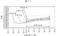
まず、図11は、本発明の一実施例である電子機器の上下カバー構造の間隙比率(G/d0)の値ごとの先端比率(L/d0)と抗力係数(CD値)の関係を示すグラフであり、G/d0の値ごとのL/d0とCD値の関係の実験結果をグラフに表した。ここでは、CD値は0.9(従来比約35%減)を基準とし、CD値が0.9以下となるG/d0とL/d0の範囲および最適値について説明する。
上述した様に、上下カバー8,13がない状態の電子機器1のCD値は1.40である。
一方、上下カバー8,13がある状態の電子機器1は、例えばG/d0=0.10とした場合、L/d0=約-0.05~約0.40のときにCD値は0.90以下となり、L/d0=約0.00のときにCD値は0.6(従来比約57%減)と、最も低くなる。
また、G/d0=0.20とした場合、L/d0=約-0.08~約0.40のときにCD値は0.90以下となり、L/d0=約0.00のときにCD値はと0.49(従来比65約%減)最も低くなる。
また、G/d0=0.30とした場合、L/d0=約-0.20~約0.40のときにCD値は0.90以下となり、L/d0=約-0.10のときにCD値は0.40(従来比約71%減)と最も低くなる。
また、G/d0=0.40とした場合、L/d0=約-0.30~約0.40のときにCD値は0.90以下となり、L/d0=約-0.20のときにCD値は0.34(従来比約76%減)と最も低くなる。
一方、上下カバー8,13がある状態の電子機器1は、例えばG/d0=0.10とした場合、L/d0=約-0.05~約0.40のときにCD値は0.90以下となり、L/d0=約0.00のときにCD値は0.6(従来比約57%減)と、最も低くなる。
また、G/d0=0.20とした場合、L/d0=約-0.08~約0.40のときにCD値は0.90以下となり、L/d0=約0.00のときにCD値はと0.49(従来比65約%減)最も低くなる。
また、G/d0=0.30とした場合、L/d0=約-0.20~約0.40のときにCD値は0.90以下となり、L/d0=約-0.10のときにCD値は0.40(従来比約71%減)と最も低くなる。
また、G/d0=0.40とした場合、L/d0=約-0.30~約0.40のときにCD値は0.90以下となり、L/d0=約-0.20のときにCD値は0.34(従来比約76%減)と最も低くなる。
以上の結果から、特にL/d0=約-0.05~約0.40のときに、G/d0が測定したどの様な値であっても、上下カバー8,13がある状態の電子機器1のCD値は0.90以下となり、上下カバー8,13がない場合に比べてCD値を35%以上低減することができる。また、例えばG/d0=0.40でL/d0=-0.20のときに、CD値は最小値の0.34となり、上下カバー8,13がない場合に比べて約76%低減することができる。
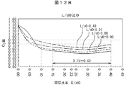
次に、図12Aのグラフおよび図12Bのグラフは、本発明の一実施例である電子機器の上下カバー構造の先端比率(L/d0)の値ごとの間隙比率(G/d0)と抗力係数(CD値)の関係を示すグラフであり、L/d0の値ごとのG/d0とCD値の関係の実験結果をグラフに表した。ここでは、CD値は0.75(従来比約46%減)を基準とし、CD値が0.75以下となるG/d0とL/d0の範囲および最適値について説明する。
例えばL/d0=-0.10とした場合、G/d0=約0.23~約0.40のときにCD値は0.75以下となり、G/d0=約0.35のときにCD値は0.40(従来比役71%減)と最も低くなる。
また、L/d0=-0.06とした場合、G/d0=約0.16~約0.40のときにCD値は0.75以下となり、L/d0=約0.30のときにCD値は0.40(従来比役71%減)と最も低くなる。
また、L/d0=-0.04とした場合、G/d0=約0.11~約0.40のときにCD値は0.75以下となり、L/d0=約0.30のときにCD値は0.41(従来比役70%減)と最も低くなる。
また、L/d0=0.00とした場合、G/d0=約0.08~約0.40のときにCD値は0.75以下となり、G/d0=約0.30のときにCD値は0.43(従来比役69%減)と最も低くなる。
また、L/d0=0.08とした場合、G/d0=約0.06~約0.40のときにCD値は0.75以下となり、L/d0=約0.30のときにCD値は0.49(従来比役65%減)と最も低くなる。
また、L/d0=0.24とした場合、G/d0=約0.08~約0.40のときにCD値は0.75以下となり、L/d0=約0.30のときにCD値は0.57(従来比役59%減)と最も低くなる。
また、L/d0=0.40とした場合、G/d0=約0.15~約0.40のときにCD値は0.75以下となり、L/d0=約0.30のときにCD値は0.63(従来比役55%減)と最も低くなる。
また、L/d0=-0.06とした場合、G/d0=約0.16~約0.40のときにCD値は0.75以下となり、L/d0=約0.30のときにCD値は0.40(従来比役71%減)と最も低くなる。
また、L/d0=-0.04とした場合、G/d0=約0.11~約0.40のときにCD値は0.75以下となり、L/d0=約0.30のときにCD値は0.41(従来比役70%減)と最も低くなる。
また、L/d0=0.00とした場合、G/d0=約0.08~約0.40のときにCD値は0.75以下となり、G/d0=約0.30のときにCD値は0.43(従来比役69%減)と最も低くなる。
また、L/d0=0.08とした場合、G/d0=約0.06~約0.40のときにCD値は0.75以下となり、L/d0=約0.30のときにCD値は0.49(従来比役65%減)と最も低くなる。
また、L/d0=0.24とした場合、G/d0=約0.08~約0.40のときにCD値は0.75以下となり、L/d0=約0.30のときにCD値は0.57(従来比役59%減)と最も低くなる。
また、L/d0=0.40とした場合、G/d0=約0.15~約0.40のときにCD値は0.75以下となり、L/d0=約0.30のときにCD値は0.63(従来比役55%減)と最も低くなる。
以上の結果から、特にG/d0=約0.23~約0.40のときに、G/d0が測定したどの様な値であっても、上下カバー8,13がある状態の電子機器1のCD値は0.75以下となり、上下カバー8,13がない場合に比べてCD値を46%以上低減することができる。
ここで、図12Aと図12Bのグラフから、L/d0<0の場合とL/d0≧0の場合とでは、それぞれ特性が異なることがわかる。以下にL/d0<0の場合とL/d0≧0の場合とに分けて、それぞれCD値が安定的に低くなるG/d0とL/d0の範囲について説明する。
まず、図12Aのグラフを用いて、L/d0<0の場合、すなわち上カバー8の前方端部10aおよび下カバー13の前方端部15aが電子機器1の上面2および下面3と同じ位置か電子機器1の外側方向(負方向)に浮いている場合について説明する。
図12Aのグラフを見ると、L/d0<0の場合、G/d0=約0.25~約0.40のときに特性が緩やかになり、CD値を0.6(従来比約57%減)以下に、CD値の変動が少なく安定的に低減できる。
図12Aのグラフを見ると、L/d0<0の場合、G/d0=約0.25~約0.40のときに特性が緩やかになり、CD値を0.6(従来比約57%減)以下に、CD値の変動が少なく安定的に低減できる。
次に、図12Bのグラフを用いてL/d0≧0の場合、すなわち上カバー8の前方端部10aおよび下カバー13の前方端部15aが電子機器1の上面2および下面3よりも電子機器1の中心方向(正方向)にせり出している場合について説明する。
図12Bのグラフを見ると、L/d0≧0の場合、G/d0=約0.10~約0.40のときに特性が緩やかになり、CD値を0.9(従来比約35%減)以下に、CD値の変動が少なく安定的に低減できる。
図12Bのグラフを見ると、L/d0≧0の場合、G/d0=約0.10~約0.40のときに特性が緩やかになり、CD値を0.9(従来比約35%減)以下に、CD値の変動が少なく安定的に低減できる。
以上、図11、図12A、および図12Bから読み取れる結果を纏めると、特にL/d0=約-0.05~0.40であれば、G/d0がいかなる値においても上下カバー8,13がない場合に比べてCD値をより安定的に低減することができる。また、L/d0=0.00であれば、G/d0=約0.10~0.40におけるいかなる値においてもCD値を0.6(従来比約57%減)以下に安定的に低減することができる。また、特にG/d0=約0.25~0.40であれば、L/d0がいかなる値においても上下カバー8,13がない場合に比べてCD値をより安定的に低減することができる。また、特に、G/d0=0.30であれば、ほぼすべてのL/d0の値においてCD値のほぼ最小値となり、最も安定的にCD値を低減することができる。
なお、ここでは、上下カバー8,13がある状態の電子機器1について、L/d0が0.40より大きい場合およびG/d0が0.40より大きい場合について図示していないが、G/d0は0.40より大きくてもCD値低減の効果は得られ、また、L/d0は上下カバーどちらか一方の場合は0.40より大きくても、上下カバー共にある場合には0.50未満であればCD値低減の効果は得られるが、それぞれ0.40より大きい値をとる場合には、実用上、他の性能を圧迫する等、効果的ではないため記載していない。
ただし、電子機器1が例えばカメラであった場合、その前面4にはガラス面が設けられ、ガラス面を介して光を取り込むことになるため、L/d0の値が大きすぎると上カバー8の前方端部10aおよび下カバー13の前方端部15aがカメラの画角に写り込んでしまう。そのため、この場合はL/d0は大き過ぎない値(例えばL/d0≦0.40の範囲)で設定するのが望ましい。
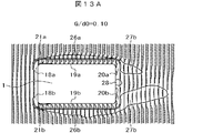
次に、図13A、図13B、および図13Cを用いて、G/d0の値の違いによる風の流れと逆流領域の発生の違いについて説明する。図13A、図13B、および図13Cは本発明の一実施例である電子機器の上下カバー構造の他の実施例における間隙比率(G/d0)の値ごとの右側面側から見た風の流れを示す断面図であり、L/d0の値を例えば0.14に固定したときの(図13A)G/d0=0.10、(図13B)G/d0=0.30、(図13C)G/d0=0.40におけるデータである。ここでの各構成と基本的な風の流れは図9に示す場合と同様であるため、説明は省略する。
図13AはG/d0=0.10の場合、すなわち電子機器1と上下カバー8,13との間隙が狭い場合の風の流れを示す断面図である。電子機器1と上下カバー8,13との間隙が狭いため、間隙に流れる風の量が少なく、上下カバー8,13の外側を流れる風の量が多くなる。電子機器1と上下カバー8,13との間隙に流れる風により、電子機器1の上下面2,3に沿って逆流領域21a,bがわずかに発生し、また、上下カバー8,13の前方湾曲部9a,14aおよび後方湾曲部9b,14bの内側にそれぞれ逆流領域がわずかに発生する。また、上下カバー8,13の外面を沿って流れる風により、上下カバー8,13の外面に沿って逆流領域26a,bが大きく発生する。つまり、電子機器1と上下カバー8,13との間隙に発生する逆流領域は少ないが、上下カバー8,13の外面に沿って発生する逆流領域26a,bが大きくなる。
図13BはG/d0=0.30の場合、すなわち電子機器1と上下カバー8,13との間隙が中くらいの場合の風の流れを示す断面図である。電子機器1と上下カバー8,13との間隙が狭くも広くもなくバランスがとれているため、間隙に流れる風の量と上下カバー8,13の外側を流れる風の量のバランスが良い。電子機器1と上下カバー8,13との間隙に流れる風により、電子機器1の上下面2,3に沿って逆流領域21a,bが発生し、また、上下カバー8,13の天井面と前方湾曲部9a,14aおよび後方湾曲部9b,14bの内側にそれぞれ逆流領域が発生する。また、上下カバー8,13の外面を沿って流れる風により、上下カバー8,13の外面に沿って逆流領域26a,bがわずかに発生する。つまり、電子機器1と上下カバー8,13との間隙のバランスが取れていれば、電子機器1と上下カバー8,13との間隙に発生する逆流領域も、上下カバー8,13の外面に沿って発生する逆流領域26a,bも小さく、カバーの内外での逆流領域が合計で小さくなる。
図13CはG/d0=0.40の場合、すなわち電子機器1と上下カバー8,13との間隙が広い場合の風の流れを示す断面図である。電子機器1と上下カバー8,13との間隙が広いため、間隙に流れる風の量が多く、電子機器1と上下カバー8,13との間隙に流れる風により、電子機器1の上下面2,3に沿って逆流領域21a,bが大きく発生し、また、上下カバー8,13の天井面と前方湾曲部9a,14aおよび後方湾曲部9b,14bの内側にそれぞれ逆流領域が大きく発生する。また、上下カバー8,13の外面を沿って流れる風により、上下カバー8,13の外面に沿って逆流領域26a,bがわずかに発生する。つまり、上下カバー8,13の外面に沿って発生する逆流領域26a,bは少ないが、電子機器1と上下カバー8,13との間隙に発生する逆流領域が大きくなる。
すなわち、ここでは、電子機器1と上下カバー8,13との間隙は、広すぎず、狭すぎない程度(本実施例の場合G/d0=0.30)に設定することが望ましい。
総括すると、電子機器とカバーとの間隙を狭くすることとカバーの先端の長さを長くすることは、間隙に流れ込む風の量を少なくしてカバーの外側へ流れる風の量を多くすることである。一方、電子機器とカバーとの間隙を広くすることとカバーの先端の長さを短くすることは、間隙に流れ込む風の量を多くしてカバーの外側へ流れる風の量を少なくすることである。間隙に流れ込む風の量とカバーの外側へ流れる風の量は、どちらかに偏るのではなく、バランスが大切であり、バランスが良くなる様に電子機器とカバーとの間隙の長さおよびカバーの先端の長さを設定することが重要である。
なお、ここではL/d0の値を0.14に固定して説明したが、上下カバーの先端同士がくっつくL/d0=0.5より小さな値であれば、他の値においても同様の効果を得ることができる。また、ここでは上下カバーが共に装着された場合を説明したが、上カバーのみまたは下カバーのみ装着されている場合でも効果があることは言うまでもない。
以上のことから、本実施例によれば、電子機器とカバーとの間隙の幅とカバーの先端の長さを適切に設定することで、カバーがない場合に比べてCD値を大幅に低減することが出来、ひいては電子機器が受ける抗力を大幅に低減することが出来る。
また、電子機器が受ける抗力が低減されることで、電子機器が風に煽られることが少なくなり、電子機器の正常な運用状態を継続することが可能となる。
また、電子機器が受ける抗力が低減されることで、電子機器自体の耐久性が向上する。さらに、電子機器が受ける抗力が低減されることで、電子機器が固定されているポール等の土台への負荷も軽減され、電子機器のみならず土台の耐久性が向上する。
また、例えば電子機器がカメラである場合には、雲台と呼ばれる水平方向(パン)と垂直方向(チルト)に向きを旋回させる装置に取り付けられ、撮像方向を自由に動かして撮像することがあるが、このとき、カメラが受ける抗力が大きいと、旋回動作の際に大きなパワーが必要となり、多くの消費電力量が必要である。本発明のカバー構造を適用すれば、電子機器が受ける抗力が低減されることで、カメラが受ける抗力が小さくなり、旋回動作の際に小さなパワーで済み、省電力化することが出来る。さらに、雲台のパワーが少なくて済むことで、雲台を小型化でき、カメラと雲台の装置全体としてコストを少なくすることができる。また、カメラが風に煽られて画角がずれることも少なくなり、良好な撮像動作を保つことが出来る。
図14は、本発明の一実施例である電子機器の山型カバー構造の斜視図である。上記実施例1とは上カバー8´の形状が異なり、本実施例では上カバー8´が、左湾曲部11a´と右湾曲部11b´からそれぞれ中央に向かって山型になっている。なお、本実施例では実施例1の上カバー8の構成と対応する部分に“´”を付けてある。また、上カバー8´の構成と、電子機器1と上カバー8との間隙に流れる風の流れについては実施例1と大体同様であるため省略する。また、電子機器1とカバー8との接続構造についても実施例1と同様の構造をとれば良いため説明は省略する。
上カバー8´が山型であることで、先端比率L/d0の値の変化によるCD値の変化は、実施例2に記載したデータと変わらないが、間隙比率G/d0の値については考慮が必要である。この場合、G/d0は図12Aおよび図12BにおいてCD値が低減される値の範囲で左右の端部および中央の山頂部の高さを設定すれば良い。L/d0<0とした場合、例えば、G/d0は約0.25~約0.40の範囲で高さを設定すれば良く、左右の端部はG/d0=0.25で中央の山頂部はG/d0=0.40等といった山型を形成すれば良い。また、L/d0≧0とした場合、例えば、G/d0は約0.10~約0.40の範囲で高さを設定すれば良く、例えば左右の端部はG/d0=0.10で中央の山頂部はG/d0=0.40とすれば良い。また、L/d0の値に関係なく山型を形成したい場合は、例えば、G/d0は約0.25~約0.40の範囲で高さを設定すれば良く、例えば左右の端部はG/d0=0.25、中央の山頂部はG/d0=0.40等といった山型を形成すれば良い。
本実施例によれば、上カバー8´が山型になっていることで、上カバー8´の上に落ちてきた雪やゴミ等が集積することなく滑り落ちる。これにより、電子機器が風により受ける抗力と雪やゴミ等の集積により受ける負荷の双方を同時に軽減することができる。
また、上カバー8´の左右の端部と中央の山頂部の高さの差を大きくすれば、山の傾斜が急となって雪やゴミ等が良く滑り落ちて集積しにくくなり、差を小さくすればG/d0のCD値低減の効果のより高い範囲の値を選択できることとなって風により受ける抗力をより低減することができるため、環境に応じてより適した形状で運用することができる。
図15は本発明の一実施例である電子機器の山型上下カバー構造の斜視図である。本実施例は、実施例2とは下カバー13´および下カバー13´が山型である点で異なり、実施例3とは上カバー8´と同形状の下カバー13´を、電子機器1に対する上カバー8´の関係と同じ関係で設けた点で異なる。なお、本実施例では実施例2の上下カバー8,13の構成と対応する部分に“´”を付けてある。また、下カバー13´の構成と、電子機器1と下カバー13´との間隙に流れる風の流れについては実施例2と大体同様であるため省略する。また、電子機器1とカバー8との接続構造についても実施例1と同様の構造をとれば良いため説明は省略する。なお、ここでは、下カバー13´は上カバー8´と同じ山型構造となっているが、実施例2と同様に山型でない構造をとっても良い。
本実施例によれば、実施例3の様に電子機器が風により受ける抗力と雪やゴミ等の集積により受ける負荷の双方を同時に軽減することができ、さらに下カバーがあることで、電子機器が風により受ける抗力を実施例3に比べてより低減することができる。
なお、上述してきた実施形態では、例として前方から後方へ風が吹き付ける場合と左方から風が吹き付ける場合について説明したが、本カバーは前後左右対称の形状であるため、後方から前方へ風が吹き付ける場合や右方から風が吹き付ける場合においても同様の作用効果をもたらすことができる。
図16および図17を用いて、電子機器の上下左右方向を覆う様に包囲する包囲カバーを備える構造について説明する。図16は本発明の一実施例である電子機器の包囲カバー構造(四角筒形)の斜視図、図17は本発明の一実施例である電子機器の包囲カバー構造(円筒形)の斜視図である。
図16、図17において、29は電子機器1の上下左右の4方を覆う包囲カバー、30aは包囲カバー29の前方湾曲部、30bは包囲カバー29の後方湾曲部、31aは包囲カバー29の前方端部であり、図示していないが31aと同様に包囲カバー29の後方端部が設けられている。本実施例は、電子機器1に上下左右の4方を覆う包囲カバーを設けた点で、上述した実施例と異なる。なお、電子機器1とカバー8との接続構造については、実施例1と同様の構造または応用した構造をとれば良い。なお、図16と図17とでは、包囲カバーの形状が四角筒形と円筒形で異なるが、基本的な間隙での風の流れは同じであり、包囲カバーの外側の風の流れが多少異なる。
本実施例においては、図16における包囲カバー29の上下左右の外側には、実施例2の上下カバー8,13の上下の外側とほぼ同様にして風が流れ、図17における包囲カバー29の外側では、前方端部31aより外側に吹き付けた風は、前方湾曲部30aおよび包囲カバー29の外面に沿って後方へと流れる。また、電子機器1の上下面2,3および左右側面4,5と包囲カバー29との間隙にも、実施例2の電子機器1の上面2と上下カバー8,13との間隙とほぼ同様にして風が流れる。
すなわち、本実施例の電子機器1および包囲カバー29を水平に切断した断面における風の流れおよび前後方向に垂直に切断した断面における風の流れは、図9における風の流れとほぼ同様になる。
なお、上下側と左右側では重力等の影響により風の流れに若干の違いが生じるかもしれないが、基本的には無視できる程度であるため、ここではほぼ同様と見なす。
また、本実施例においても、先端比率L/d0の値と間隙比率G/d0の値は、図11、図12A、および図12Bに示す実施例2の場合と同様にして値を設定することで、カバーがない場合に比べてCD値を大幅に低減することができ、ひいては電子機器が受ける抗力を大幅に低減することができる。
本実施例によれば、上下方向だけでなく左右方向もカバーで覆われていることで、例えば列車や車等に設置するという様な、前後方向から風が吹き付ける場合に、より効果的に電子機器が受ける抗力を低減することができる。
また、上下からの物理的衝撃だけでなく左右からの物理的衝撃に対する電子機器への影響も低減することができる。
また、例えば、包囲カバー29の上面を実施例4の様に山型の構造としても良く、この場合、間隙比率G/d0の値は、実施例3の様に効果の出る任意の範囲で設定すれば良い。これにより、実施例3の様に電子機器が風により受ける抗力と雪やゴミ等の集積により受ける負荷の双方を同時に軽減することができる。
上述してきた実施例における電子機器のカバー構造の説明では、カメラを想定した場合の効果を一部説明したが、カメラの他にも屋外または屋内に設置される電子機器または電子機器ではない機器等に用いることももちろん可能であり、その構成及び動作とその内容についても本発明の要旨を逸脱しない範囲で種々に変形して実施できる。
また、上述してきた実施例における電子機器のカバー構造の説明では、間隙比率G/d0および先端比率L/d0においてCD値を低減する値およびその範囲として、例えば約0.30等としてきたが、ここで約とはプラスマイナス0.025程度であれば、その効果に大きな影響はない。
また、間隙比率および先端比率は電子機器の高さを基準にして求めたが、基準は電子機器の高さのみに限定されることはなく、他にも電子機器の横の長さや幅等、電子機器またはその他のどの様な部分を基準に比率を求めても良いことは言うまでもない。
要するに本発明は、上記各実施形態そのままに限定されるものではなく、実施段階ではその要旨を逸脱しない範囲で構成要素を変形して具体化できる。また、上記各実施形態に開示されている複数の構成要素の適宜な組み合せにより種々の発明を形成できる。例えば、各実施形態に示される全構成要素から幾つかの構成要素を削除してもよい。さらに、異なる実施形態に亘る構成要素を適宜組み合せてもよい。
1:電子機器、2:電子機器上面、3:電子機器下面、4:電子機器前面、5:電子機器背面、6:電子機器左側面、7:電子機器右側面、8:上カバー、9a:上カバーの前方湾曲部、9b:上カバーの後方湾曲部、10a:上カバーの前方端部、10b:上カバーの後方端部、11a:上カバーの左湾曲部、11b:上カバーの右湾曲部、12a:上カバーの左方端部、12b:上カバーの右方端部、13:下カバー、14a:下カバーの前方湾曲部、14b:下カバーの後方湾曲部、15a:下カバーの前方端部、15b:下カバーの後方端部、16a:下カバーの左湾曲部、16b:下カバーの右湾曲部、17a:下カバーの左方端部、17b:下カバーの右方端部、18a,b,21a,b:間隙誘導領域、19a,b,22a,b:間隙流動領域、20a,b,23a,b:間隙排出領域、24a,b,25,26a,b,27a,b,28:逆流領域、29:包囲カバー、30a:包囲カバーの前方湾曲部、30b:包囲カバーの後方湾曲部、31a:包囲カバーの前方端部。
Claims (11)
- 略立方体または略直方体形状の電子機器と、少なくとも1つの略正方形または略長方形状で構成される屋根部と、前記屋根部の周囲の少なくとも1辺に設けられた湾曲部と、該湾曲部に接続される先端部とから構成されるカバーと、を備える電子機器のカバー構造であって、前記カバーは、前記電子機器との間に所定の間隙を設け、前記先端部が前記電子機器側を向く様に、前記先端部が前記電子機器のいずれかの面の対応する端部より外側に突出させて装着されることを特徴とする電子機器のカバー構造。
- 前記カバーの湾曲部は、前記屋根部の全周囲に設けられ、前記カバーは、前記先端部が前記電子機器の面の各端部より外側に突出させて装着されることを特徴とする請求項1に記載の電子機器のカバー構造。
- 前記カバーは、前記電子機器の前記カバーが装着された面と逆側の面にも装着されることを特徴とする請求項1乃至2に記載の電子機器のカバー構造。
- 略立方体または略直方体形状の電子機器と、少なくとも1つの略正方形または略長方形状で構成される屋根部と、略正方形または略長方形状の左右の側面部および下面部と、前記屋根部と前記左右の側面部および前記左右の側面部と前記下面部とをそれぞれ接続する湾曲部とから構成されるカバーまたは筒状に構成されるカバーと、を備える電子機器のカバー構造であって、前記カバーは、前記電子機器の上下左右を覆う様に装着されることを特徴とする電子機器のカバー構造。
- 前記電子機器の前記カバーが装着された面から前記屋根部までの前記間隙の距離を前記電子機器の高さで除算した値を第1の比率とし、前記カバーは、前記第1の比率が約0.25~約0.40の範囲から所定の値をとる様に電子機器に装着されることを特徴とする請求項1乃至4に記載の電子機器のカバー構造。
- 前記第1の比率が約0.30であることを特徴とする請求項5に記載の電子機器のカバー構造。
- 前記電子機器の前記カバーが装着された面の水平位置から前記カバーの前記先端部の末端までの垂直方向の距離を前記電子機器の高さで除算した値を第2の比率とし、前記カバーは、前記第2の比率が約-0.05~約0.40の範囲から所定の値をとる様に電子機器に装着されることを特徴とする請求項1乃至5に記載の電子機器のカバー構造。
- 前記第2の比率が0.00であることを特徴とする請求項7に記載の電子機器のカバー構造。
- 前記電子機器の前記カバーが装着された面の水平位置から前記カバーの前記先端部の末端までの垂直方向の距離を前記電子機器の高さで除算した値を第2の比率とし、前記カバーは、さらに、前記第2の比率が0以上のときには、前記第1の比率で約0.10~約0.40の範囲から所定の値をとる様に電子機器に装着されることを特徴とする請求項5に記載の電子機器のカバー構造。
- 前記屋根部は、2以上の略正方形または略長方形状で山型に構成され、前記電子機器の前記カバーが装着された面から前記屋根部までの前記間隙の距離を前記電子機器の高さで除算した値を第1の比率とし、前記カバーは、前記電子機器の前記カバーが装着された面から前記屋根部の両端までの間隙の距離と前記電子機器の前記カバーが装着された面から前記屋根部の中央までの間隙の距離およびその間の間隙の距離が、前記第1の比率が約0.10~約0.40の範囲からそれぞれ所定の値をとる様に電子機器に装着されることを特徴とする請求項1乃至4または請求項7乃至8に記載の電子機器のカバー構造。
- 前記電子機器は、カメラであることを特徴とする請求項1乃至10に記載の電子機器のカバー構造。
Priority Applications (1)
| Application Number | Priority Date | Filing Date | Title |
|---|---|---|---|
| CN2011900007458U CN203289527U (zh) | 2010-09-22 | 2011-03-11 | 电子设备的罩结构 |
Applications Claiming Priority (2)
| Application Number | Priority Date | Filing Date | Title |
|---|---|---|---|
| JP2010212030A JP5546403B2 (ja) | 2010-09-22 | 2010-09-22 | カバー付き電子機器 |
| JP2010-212030 | 2010-09-22 |
Publications (1)
| Publication Number | Publication Date |
|---|---|
| WO2012039155A1 true WO2012039155A1 (ja) | 2012-03-29 |
Family
ID=45873653
Family Applications (1)
| Application Number | Title | Priority Date | Filing Date |
|---|---|---|---|
| PCT/JP2011/055790 Ceased WO2012039155A1 (ja) | 2010-09-22 | 2011-03-11 | 電子機器のカバー構造 |
Country Status (3)
| Country | Link |
|---|---|
| JP (1) | JP5546403B2 (ja) |
| CN (1) | CN203289527U (ja) |
| WO (1) | WO2012039155A1 (ja) |
Families Citing this family (2)
| Publication number | Priority date | Publication date | Assignee | Title |
|---|---|---|---|---|
| JP5700732B2 (ja) * | 2014-01-23 | 2015-04-15 | 株式会社日立国際電気 | カバー付き電子機器 |
| CN104092928A (zh) * | 2014-07-18 | 2014-10-08 | 天津市嘉杰电子有限公司 | 摄像机安装板固定结构 |
Citations (5)
| Publication number | Priority date | Publication date | Assignee | Title |
|---|---|---|---|---|
| JPH10210331A (ja) * | 1997-01-16 | 1998-08-07 | Ikegami Tsushinki Co Ltd | 屋外用監視カメラのフード取付装置 |
| JPH10341370A (ja) * | 1997-06-10 | 1998-12-22 | Yokogawa Electric Corp | パンチルトカメラ装置 |
| JPH1175094A (ja) * | 1997-08-29 | 1999-03-16 | Mitsubishi Electric Corp | 撮像装置システム |
| JP2004248153A (ja) * | 2003-02-17 | 2004-09-02 | Sanyo Electric Co Ltd | 監視カメラ装置 |
| JP2006140712A (ja) * | 2004-11-11 | 2006-06-01 | Fujinon Corp | 雲台装置 |
-
2010
- 2010-09-22 JP JP2010212030A patent/JP5546403B2/ja not_active Expired - Fee Related
-
2011
- 2011-03-11 CN CN2011900007458U patent/CN203289527U/zh not_active Expired - Lifetime
- 2011-03-11 WO PCT/JP2011/055790 patent/WO2012039155A1/ja not_active Ceased
Patent Citations (5)
| Publication number | Priority date | Publication date | Assignee | Title |
|---|---|---|---|---|
| JPH10210331A (ja) * | 1997-01-16 | 1998-08-07 | Ikegami Tsushinki Co Ltd | 屋外用監視カメラのフード取付装置 |
| JPH10341370A (ja) * | 1997-06-10 | 1998-12-22 | Yokogawa Electric Corp | パンチルトカメラ装置 |
| JPH1175094A (ja) * | 1997-08-29 | 1999-03-16 | Mitsubishi Electric Corp | 撮像装置システム |
| JP2004248153A (ja) * | 2003-02-17 | 2004-09-02 | Sanyo Electric Co Ltd | 監視カメラ装置 |
| JP2006140712A (ja) * | 2004-11-11 | 2006-06-01 | Fujinon Corp | 雲台装置 |
Also Published As
| Publication number | Publication date |
|---|---|
| JP5546403B2 (ja) | 2014-07-09 |
| JP2012070139A (ja) | 2012-04-05 |
| CN203289527U (zh) | 2013-11-13 |
Similar Documents
| Publication | Publication Date | Title |
|---|---|---|
| JP5980180B2 (ja) | 軸流ファン、及び、その軸流ファンを有する空気調和機 | |
| CN101454565B (zh) | 具有渐扩后缘的风轮机叶片 | |
| CN100425826C (zh) | 转子叶片末端、转子叶片及风力发电设备 | |
| ES2635338T3 (es) | Sistema de protección contra rayos para una paleta de turbina eólica | |
| JP6840172B2 (ja) | 流体機器 | |
| CN108443226A (zh) | 一种阶梯蜗壳结构及离心风机及鼓风装置 | |
| KR20130041263A (ko) | 풍차 날개 및 이를 구비한 풍력 발전 장치와 풍차 날개의 설계 방법 | |
| JP5546403B2 (ja) | カバー付き電子機器 | |
| US7334986B2 (en) | Centrifugal fan | |
| JP5700732B2 (ja) | カバー付き電子機器 | |
| AU2007229443A1 (en) | Polygonal overhead cable | |
| JPWO2015121989A1 (ja) | 軸流送風機 | |
| US11965522B2 (en) | Impeller | |
| US8382427B2 (en) | Blower fan | |
| CN106368741A (zh) | 一种具有小翼肋条叶尖的叶片及使用该叶片的涡轮 | |
| CN215765277U (zh) | 蜗壳、风机及吸油烟机 | |
| CN108397835A (zh) | 导风圈结构、空调室外机及空调器 | |
| WO1999017306A1 (en) | Overhead wire | |
| CN100485193C (zh) | 送风机 | |
| JP2005132314A (ja) | 船舶 | |
| EP2940292B1 (en) | Device for a rotor blade of a wind turbine | |
| JP4134053B2 (ja) | 斜風対応型防雪柵 | |
| CN105946508A (zh) | 车用空调及其空调外罩 | |
| JP2010261613A (ja) | 天井埋込形換気扇 | |
| CN207377858U (zh) | 吸尘器电机中的叶轮和吸尘器电机 |
Legal Events
| Date | Code | Title | Description |
|---|---|---|---|
| WWE | Wipo information: entry into national phase |
Ref document number: 201190000745.8 Country of ref document: CN |
|
| 121 | Ep: the epo has been informed by wipo that ep was designated in this application |
Ref document number: 11826601 Country of ref document: EP Kind code of ref document: A1 |
|
| NENP | Non-entry into the national phase |
Ref country code: DE |
|
| 122 | Ep: pct application non-entry in european phase |
Ref document number: 11826601 Country of ref document: EP Kind code of ref document: A1 |