WO2012020461A1 - シリコンインゴットの製造装置および製造方法 - Google Patents
シリコンインゴットの製造装置および製造方法 Download PDFInfo
- Publication number
- WO2012020461A1 WO2012020461A1 PCT/JP2010/006740 JP2010006740W WO2012020461A1 WO 2012020461 A1 WO2012020461 A1 WO 2012020461A1 JP 2010006740 W JP2010006740 W JP 2010006740W WO 2012020461 A1 WO2012020461 A1 WO 2012020461A1
- Authority
- WO
- WIPO (PCT)
- Prior art keywords
- plasma
- silicon
- electrode
- silicon ingot
- heating
- Prior art date
- Legal status (The legal status is an assumption and is not a legal conclusion. Google has not performed a legal analysis and makes no representation as to the accuracy of the status listed.)
- Ceased
Links
Images

Classifications
-
- C—CHEMISTRY; METALLURGY
- C01—INORGANIC CHEMISTRY
- C01B—NON-METALLIC ELEMENTS; COMPOUNDS THEREOF; METALLOIDS OR COMPOUNDS THEREOF NOT COVERED BY SUBCLASS C01C
- C01B33/00—Silicon; Compounds thereof
- C01B33/02—Silicon
- C01B33/021—Preparation
-
- C—CHEMISTRY; METALLURGY
- C30—CRYSTAL GROWTH
- C30B—SINGLE-CRYSTAL GROWTH; UNIDIRECTIONAL SOLIDIFICATION OF EUTECTIC MATERIAL OR UNIDIRECTIONAL DEMIXING OF EUTECTOID MATERIAL; REFINING BY ZONE-MELTING OF MATERIAL; PRODUCTION OF A HOMOGENEOUS POLYCRYSTALLINE MATERIAL WITH DEFINED STRUCTURE; SINGLE CRYSTALS OR HOMOGENEOUS POLYCRYSTALLINE MATERIAL WITH DEFINED STRUCTURE; AFTER-TREATMENT OF SINGLE CRYSTALS OR A HOMOGENEOUS POLYCRYSTALLINE MATERIAL WITH DEFINED STRUCTURE; APPARATUS THEREFOR
- C30B11/00—Single-crystal growth by normal freezing or freezing under temperature gradient, e.g. Bridgman-Stockbarger method
- C30B11/001—Continuous growth
-
- C—CHEMISTRY; METALLURGY
- C30—CRYSTAL GROWTH
- C30B—SINGLE-CRYSTAL GROWTH; UNIDIRECTIONAL SOLIDIFICATION OF EUTECTIC MATERIAL OR UNIDIRECTIONAL DEMIXING OF EUTECTOID MATERIAL; REFINING BY ZONE-MELTING OF MATERIAL; PRODUCTION OF A HOMOGENEOUS POLYCRYSTALLINE MATERIAL WITH DEFINED STRUCTURE; SINGLE CRYSTALS OR HOMOGENEOUS POLYCRYSTALLINE MATERIAL WITH DEFINED STRUCTURE; AFTER-TREATMENT OF SINGLE CRYSTALS OR A HOMOGENEOUS POLYCRYSTALLINE MATERIAL WITH DEFINED STRUCTURE; APPARATUS THEREFOR
- C30B29/00—Single crystals or homogeneous polycrystalline material with defined structure characterised by the material or by their shape
- C30B29/02—Elements
- C30B29/06—Silicon
Definitions
- the present invention relates to a silicon manufacturing apparatus and manufacturing method capable of manufacturing a polycrystalline silicon ingot by applying a continuous casting technique using electromagnetic induction, and in particular, a substrate material for a solar cell using plasma heating by a plasma arc.
- the present invention relates to a silicon manufacturing apparatus and manufacturing method capable of manufacturing a polycrystalline silicon ingot used as a raw material without deteriorating solar cell characteristics.
- electromagnetic casting apparatus a continuous casting apparatus by electromagnetic induction (hereinafter referred to as “electromagnetic casting apparatus”) to which a bottomless cooling mold divided in the circumferential direction is attached is used, a dissolved substance (here, molten silicon), a mold, Can hardly be in contact with each other, so that an ingot (silicon ingot) free from impurity contamination can be produced. Since there is no contamination from the mold, there is an advantage that it is not necessary to use a high-purity material as the material of the mold, and since it can be continuously cast, the manufacturing cost can be greatly reduced. Therefore, the electromagnetic casting apparatus has been conventionally applied to the production of polycrystalline silicon used as a substrate material for solar cells.
- FIG. 3 is a diagram schematically showing a configuration example of an electromagnetic casting apparatus used for producing polycrystalline silicon.
- the heating induction coil 2 longitudinally long copper plate pieces that can be water-cooled are parallel to the winding axis direction of the induction coil 2, and are mutually in the induction coil 2.
- a space surrounded by the plate-like pieces constitutes a mold (that is, a bottomless cooling mold in which a side wall portion is water-cooled).
- a water-cooled copper mold having a plate-like piece as a copper piece is usually used for the cooling mold 1.
- a support base 4 that can move downward is provided at the lower end position of the induction coil 2 for heating (that is, the position corresponding to the bottom of the cooling mold 1).
- a heat retaining device 6 for heating the solidified ingot (silicon ingot 5) to prevent rapid cooling is installed below the induction coil 2 for heating.
- the soaking tube 7 is attached.
- the silicon ingot 5 is drawn downward by a drawing device (not shown).
- a raw material charging machine 15 capable of charging the raw material into the mold 1 during melting is installed. Furthermore, in this example, a plasma torch 3 for heating the raw material silicon is attached above the mold 1 as necessary.
- These devices are installed in a sealed container 8 so that the molten silicon 11 and the high-temperature silicon ingot 5 do not come into direct contact with the atmosphere.
- the inside of the container 8 is replaced with an inert gas, It is comprised so that continuous casting can be performed in the pressurized state.
- the silicon raw material in the mold 1 receives a force in the normal direction on the surface of the molten silicon 11 due to the interaction between the magnetic field generated by the current on the inner wall of the mold 1 and the current on the surface of the molten silicon 11. Dissolved in the state.
- the support 4 After the molten silicon 11 is sufficiently homogenized, if the support 4 is moved downward little by little, cooling starts by moving away from the induction coil 2 and unidirectional solidification toward the molten silicon 11 in the mold 1. As a result, the silicon ingot 5 having a cross section having the same shape as the mold cross section is formed.
- the polycrystalline silicon ingot 5 can be continuously produced by continuing the heat melting, drawing, and raw material supply.
- Polycrystalline silicon produced using this electromagnetic casting device is highly purified, and its quality, especially conversion efficiency when used as a substrate for solar cells (extracting incident light energy by converting it into electrical energy)
- many technologies have been developed. At that time, the development of a method using both electromagnetic induction heating by an induction coil and plasma heating by a plasma arc is being actively promoted.
- Patent Document 1 discloses a silicon continuous casting method in which the quality as a solar cell is improved by using both electromagnetic induction heating and plasma heating. According to the casting method described in the same document, it is possible to reduce the burden of electromagnetic induction heating by using plasma heating in combination with raw material melting during casting, and the reduction reduces thermal convection of molten silicon due to electromagnetic force, The solid-liquid interface is flattened by suppressing the heat flow rate to. As a result, the temperature gradient in the radial direction of the silicon ingot immediately after solidification is reduced, the thermal stress generated in the crystal is relaxed, and the generation of crystal defects that deteriorate the conversion efficiency of the solar cell is suppressed.
- a plasma arc torch in order to make the best use of the effect of plasma heating, is scanned in the horizontal direction on the silicon melt instead of being fixed to the center of the silicon melt in the crucible. Further, it is considered that a plasma arc is preferably a transfer type plasma arc that easily obtains a large output necessary for silicon casting.
- Patent Document 2 as a method for producing a high-purity polycrystalline silicon ingot used for solar cells, a raw material supplied in a bottomless crucible is melted by electromagnetic induction heating to produce a silicon ingot.
- the plasma torch used here may be either a transfer type or a non-transfer type.
- Patent Document 3 discloses a method for producing high purity metal Si by plasma melting raw material metal Si without electromagnetic induction heating. That is, during plasma melting, by adding water vapor to the molten Si, B and C are oxidized to BO and CO, and a large number of fine hydrogen gas bubbles generated from the added NH 3 gas are contained in the bubbles. In this method, BO and CO gas are taken in and B and C are efficiently removed.
- Patent Documents 1 to 3 describe the material of the plasma electrode. .
- the polarity of the electrode is not particularly described, it can be seen from the description of each drawing of Patent Document 1 or 3 that the plasma electrode is a cathode.
- Non-Patent Document 1 describes the use of plasma, which is used as a welding heat source, in the field of metal refining, in which a plasma electrode is a cathode (cathode) and a workpiece is an anode (anode).
- a drawing of the constructed plasma torch (FIGS. 7 and 1 of Non-Patent Document 1) is described.
- a high melting point metal such as tungsten (W) is used for the cathode (that is, plasma electrode) in a non-oxidizing atmosphere and zirconium (Zr) is used in an oxidizing atmosphere.
- W is a high melting point material having a melting point of 3400 ° C.
- the W electrode is damaged by the impact of the plasma arc, and W vapor is generated.
- Metal contaminants are introduced into the atmosphere, which may cause ingot contamination. Because.
- the metal impurity becomes a trap (capture) level of the recombination of carriers generated by light and disappears, thereby lowering the conversion efficiency. Therefore, the quality of polycrystalline silicon used as a substrate material for solar cells is improved. In further raising, contamination with metal (W) is a problem that cannot be overlooked.
- the present invention has been made in view of such a situation.
- the effect of contamination by a metal on a polycrystalline silicon ingot used as a material for a substrate material of a solar cell by combining plasma induction by plasma arc with electromagnetic induction heating.
- An object of the present invention is to provide a silicon ingot manufacturing apparatus and a manufacturing method that can be manufactured without reducing solar cell characteristics (particularly, conversion efficiency).
- the present inventors investigated the influence of metal impurities mixed in polycrystalline silicon on the conversion efficiency when a solar cell is constructed using the polycrystalline silicon as a substrate.
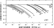
- FIG. 2 is a diagram showing the relationship between the metal impurity concentration in P-type silicon and the conversion efficiency when a solar cell is constructed, and is a diagram described in Non-Patent Document 2 described above.
- the “relative efficiency of the solar cell” on the vertical axis represents the relative efficiency by normalizing the influence of the concentration of each metal element on the conversion efficiency of the solar cell.
- the conversion efficiency when a solar cell is constructed without exception is lowered.
- the lower limit value of the concentration that affects the conversion efficiency varies depending on the type of metal, and in the same figure, it can be said that the metal located in the right direction of the paper is a metal that does not easily affect the conversion efficiency of the solar cell.
- W which is currently used as an electrode material for a plasma torch used in combination with electromagnetic casting of silicon, lowers the conversion efficiency of a solar cell on the order of 10 12 atoms / cm 3 as a metal impurity concentration.
- Cu has an influence on the conversion efficiency only when the metal impurity concentration is on the order of 10 17 atoms / cm 3 . That is, it can be said that Cu is a metal that has a lower limit of the concentration at which the influence appears about five orders of magnitude higher than W and hardly influences the conversion efficiency of the solar cell.
- the plasma electrode In the arc discharge between the electrode of the plasma torch (plasma electrode; cathode) and the object to be heated (here, molten silicon; anode), the plasma electrode (cathode) is ionized with gas (usually Ar) molecules as a plasma medium. Ar ions collide and electron emission is promoted at the plasma electrode (cathode). Due to the collision of the Ar molecules and Ar ions, the plasma electrode is damaged and evaporated, and mixed into the plasma medium, and the electrode is consumed. In order to suppress the consumption of the electrode, it is effective to use a high melting point material for the electrode, and W has been used as the electrode material as described above. However, as shown in FIG. 2, W may reduce the conversion efficiency of the solar cell even if a very small amount evaporates.
- Cu has a melting point of 1084 ° C. and is considerably lower than W, but its concentration that has an adverse effect on the conversion efficiency of the solar cell is extremely high.
- silicon it is extremely advantageous to use Cu as a plasma electrode when plasma heating is used in combination.
- the inventors of the present invention used Cu for the plasma electrode, made a cathode as in the conventional case, and made molten silicon as the anode, and manufactured a polycrystalline silicon ingot while using electromagnetic induction heating and plasma heating together.
- the possibility of application to plasma electrodes was investigated.
- the consumption rate of the electrode is about 75 times that of the W electrode, as shown in the examples described later, but the conversion efficiency when the solar cell is configured is higher than when the W electrode is used, At least in the case of producing a polycrystalline silicon ingot for a substrate material of a solar cell, it has been found that it is sufficiently practical.
- the inventors further manufactured a polycrystalline silicon ingot in the same manner by using Cu as the plasma electrode, using the plasma electrode as the anode, and using the molten silicon as the cathode (that is, inverting the anode cathode).
- the reason why the Cu electrode is used as the anode is to avoid damage due to collision of Ar molecules and Ar ions and to suppress consumption due to evaporation of the electrode. As a result, it has been found that electrode consumption can be suppressed slightly and the relative conversion efficiency when a solar cell is constructed can be improved.
- the present invention has been made on the basis of such knowledge, and is summarized in the following (1) silicon ingot manufacturing apparatus and (2) silicon ingot manufacturing method.
- a silicon ingot manufacturing apparatus that has a plasma torch for generating a plasma arc, and is configured to pull down and solidify molten silicon downward by using both electromagnetic induction heating by the induction coil and plasma heating by the plasma arc.
- the plasma electrode is an anode and the silicon to be heated is a cathode, consumption of the electrode is suppressed to a small extent, and conversion efficiency when a solar cell is configured is improved. This is desirable.
- the silicon raw material is charged into a bottomless cooling mold, melted by using electromagnetic induction heating and plasma heating by plasma arc in combination, and the silicon ingot is continuously solidified by lowering and solidifying the molten silicon.
- the consumption of the electrode is suppressed to a minimum, and a solar cell is configured. This is desirable because it can improve conversion efficiency.
- the silicon ingot manufacturing apparatus of the present invention is a manufacturing apparatus having a plasma torch in addition to an induction coil as a heating source and using copper as a plasma electrode.
- the plasma electrode copper electrode
- Preferred embodiments are employed. If this manufacturing apparatus is used, it is possible to manufacture a polycrystalline silicon ingot used as a substrate material for a solar cell, in which the influence of metal contamination is suppressed and conversion efficiency is maintained high.
- the method for producing a silicon ingot of the present invention can be easily implemented by using the production apparatus of the present invention.
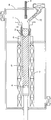
- FIG. 1 is a longitudinal sectional view showing a schematic configuration example of a silicon ingot manufacturing apparatus according to the present invention.
- FIG. 1 (a) is an overall view
- FIGS. 2 (b) and 2 (c) are partially enlarged views of a plasma torch. is there. It is a figure which shows the relationship between the metal impurity density
- the silicon ingot manufacturing apparatus of the present invention is premised on an electromagnetic casting apparatus having a conductive bottomless cooling mold in which a part in the axial direction is divided into a plurality of parts in the circumferential direction and an induction coil surrounding the mold. Yes.
- the premise of such an electromagnetic casting apparatus is that, when producing polycrystalline silicon used as a substrate material for a solar cell, casting is performed in a mold with almost no contact between the molten silicon and the mold. This is because it is possible to manufacture a silicon ingot that is free from metal contamination and can maintain good conversion efficiency. It is not necessary to use a high-purity material as the mold material, and since it can be continuously cast, the manufacturing cost can be significantly reduced.
- the manufacturing apparatus of the present invention further includes a plasma torch for generating a plasma arc, which is installed as a heating source so as to be movable up and down above the cooling mold.
- a plasma torch for generating a plasma arc which is installed as a heating source so as to be movable up and down above the cooling mold.
- a feature of the manufacturing apparatus of the present invention is that copper (Cu) is used as a plasma electrode disposed in a plasma torch.
- FIG. 1 is a longitudinal sectional view showing a schematic configuration example of a silicon ingot manufacturing apparatus according to the present invention, where (a) is an overall view, and (b) and (c) are partially enlarged views of a plasma torch.
- the manufacturing apparatus of the present invention includes a conductive bottomless cooling mold 1 and an induction coil 2 surrounding the mold 1, and further generates a plasma arc as a heating source.
- a plasma torch 3 is provided. The plasma torch 3 is installed above the cooling mold 1 so as to be movable up and down.
- a support base 4 that can move downward is installed. Further, a heat retaining device 6 for heating the solidified silicon ingot 5 to prevent rapid cooling is installed below the induction coil 2, and a heat equalizing cylinder 7 is disposed below the heat retaining device 6. Is attached. The silicon ingot 5 is drawn downward by the drawing device 10. These devices are installed in the sealed container 8 so that the molten silicon and the high-temperature silicon ingot 5 do not come into direct contact with the atmosphere.
- a plasma electrode is disposed in the plasma torch 3 and is connected to the positive electrode of the DC power source 9 in the illustrated example.
- the negative electrode of the DC power source 9 is connected to the molten silicon 11 through the drawing device 10 of the ingot 5 and the silicon ingot 5.
- FIG. 1 (b) schematically shows the state of the tip of the plasma torch 3 and its surroundings when the plasma electrode is used as a cathode according to a general method.
- An arc discharge 13 is generated between the plasma electrode 12 constituting the cathode and the molten silicon 11 constituting the anode.
- Ar molecules and ionized Ar ions collide with the plasma electrode (cathode), Cu evaporant 14 is generated and mixed in the plasma medium, and metal contaminant (Cu) is introduced into the atmosphere.
- the consumption of the electrode 12 is also great.
- Cu is significantly higher than W that has been used as a conventional plasma electrode material.
- the conversion efficiency when the battery is configured is improved as compared with the conventional case.
- the silicon ingot manufacturing apparatus of the present invention it is desirable to use Cu as the plasma electrode, and to use the plasma electrode (Cu electrode) as the anode and the molten silicon 11 as the object to be heated as the cathode.
- the consumption of the electrode is large, and although the lower limit of the metal impurity concentration that adversely affects the conversion efficiency of the solar cell is extremely high, metal contamination in the atmosphere A substance (Cu) is introduced. In order to improve this state, it is effective to reverse the polarity of the plasma electrode, so that the consumption of the electrode can be suppressed and the conversion efficiency when the solar cell is configured can be improved.
- FIG. 1 (c) schematically shows the tip of the plasma torch 3 connected in this way and the surrounding state.
- An arc discharge 13 is generated between the plasma electrode 12 and the molten silicon 11, but collision of Ar molecules or ionized Ar ions with the plasma electrode 12 is avoided.
- Introduction of metal contaminants (Cu) is suppressed.
- the conversion efficiency when the solar cell is configured is also improved.
- the alloy elements are considered to have a lower metal impurity concentration than Cu, which adversely affects the conversion efficiency of the solar cell. Therefore, the use of Cu alloy is used from the viewpoint of maintaining high conversion efficiency as a solar cell. It is disadvantageous.
- the plasma torch that can be used here, there are a transition type in which the object to be heated shown in FIG. 1 is a counter electrode and a non-transition type in which the generated plasma is discharged from the torch by discharging between the electrodes in the torch.
- a transition-type plasma torch with high output and high thermal efficiency is desirable.
- a silicon raw material is charged into a bottomless cooling mold, melted by using both electromagnetic induction heating and plasma heating by a plasma arc, and the melted silicon is lowered and solidified.
- the method is characterized in that Cu is used as the plasma electrode for generating the plasma arc on the premise that the silicon ingot is continuously cast by the above method. The reason for this assumption and the reason for using Cu as the plasma electrode are as described above.
- Cu is used as a plasma electrode
- a plasma electrode (Cu electrode) is used as an anode and silicon as a heated object is used as a cathode. This is because the consumption of the electrode is suppressed and the conversion efficiency when the solar cell is configured can be maintained high.
- Ar When plasma heating is used in combination, normally used Ar may be used as the plasma medium.
- Other conditions are not basically changed by changing the W electrode of the plasma torch to a Cu electrode, and may be operated in accordance with a conventional method.
- the manufacturing method of the present invention can be easily carried out by the conventional operation procedure using the above-described silicon ingot manufacturing apparatus of the present invention.
- the silicon ingot manufacturing apparatus and manufacturing method of the present invention adopts a Cu electrode as a plasma electrode by utilizing the fact that the metal impurity concentration that adversely affects the conversion efficiency of a solar cell varies greatly depending on the metal. And it is the technique of maintaining the conversion efficiency high when a solar cell is comprised. Further, by reversing the current direction in the plasma torch (reversing the anode and cathode), consumption of the Cu electrode can be minimized and conversion efficiency can be maintained higher.
- a silicon ingot having a cross-sectional dimension of 345 mm ⁇ 505 mm and a length of 7 m is manufactured.
- the consumption rate, ingot contamination by electrode material and relative conversion efficiency were investigated.
- the same investigation was performed when a conventional tungsten electrode was used.
- Plasma current 1100A
- Plasma voltage 120V
- Plasma irradiation time 70 hours
- Distance between heated object and electrode 200 mm
- the “ingot contamination amount” is obtained by collecting samples from the outer peripheral portion and the central portion in the longitudinal direction of each of the obtained ingots and dissolving them, and then ICP-MS (Inductively Coupled Plasma-Mass Spectroscopy). W or Cu was analyzed using inductively coupled high-frequency plasma spectroscopy, and converted to the number of atoms / cm 3 .
- “relative conversion efficiency” is obtained by cutting a silicon wafer from each obtained ingot, measuring the current-voltage characteristics (IV characteristics) of a solar cell configured with the wafer as a substrate, obtaining the conversion efficiency, Using Cu as an anode (in Table 1, “plus” is displayed in the “polarity” column), the conversion efficiency when plasma heating was performed was displayed as a reference (1.0).
- the electrode material is Cu (example of the present invention)
- the polarity is positive (that is, when Cu is the anode)
- the polarity is negative (that is, when Cu is the cathode)
- the electrode consumption rate was significantly reduced in the former case. This is because the collision of Ar molecules and ionized Ar ions to the Cu electrode can be avoided by using the Cu electrode as the anode.
- the amount of ingot contamination is greatly reduced, and the obtained ingot is used as a material for the solar cell.
- the conversion efficiency was very good (in Table 1, the relative conversion efficiency was 1.0).
- the relative conversion efficiency was 0.9, which was slightly lower than the former.
- the electrode material is W
- the electrode consumption rate and ingot are higher than when the electrode material is Cu.
- the amount of contamination was very low.
- W has a lower lower limit of impurity concentration that affects the conversion efficiency of the solar cell than Cu
- the relative conversion efficiency is 0.7
- the electrode material is Cu (regardless of polarity). The conversion efficiency was clearly lower than that.
- the electrode material is W and the polarity is positive (comparative example), the electrode consumption rate and the ingot contamination amount are extremely low. As a result, the electrode material is Cu and this is the anode. Although this was not the case, the conversion efficiency was good (relative conversion efficiency 0.9).
- the silicon ingot manufacturing apparatus and method of the present invention it is possible to manufacture a polycrystalline silicon ingot that is used as a substrate material of a solar cell while suppressing the influence of metal contamination and maintaining high conversion efficiency. Therefore, the present invention can be effectively used in the manufacturing field of solar cells, and can greatly contribute to the progress of natural energy utilization technology.
Landscapes
- Chemical & Material Sciences (AREA)
- Organic Chemistry (AREA)
- Engineering & Computer Science (AREA)
- Crystallography & Structural Chemistry (AREA)
- Materials Engineering (AREA)
- Metallurgy (AREA)
- Inorganic Chemistry (AREA)
- Silicon Compounds (AREA)
Abstract
無底冷却モールド(1)と、加熱用誘導コイル(2)を有し、さらに、加熱源としてプラズマトーチ(3)を有し、電磁誘導加熱とプラズマ加熱を併用するシリコンインゴットの製造装置であって、前記プラズマトーチ内に配設されたプラズマ電極(12)として銅(Cu)を用いる製造装置。前記プラズマ電極を陽極とし、被加熱物であるシリコン(11)を陰極とすれば、電極の消耗を僅少に抑えるとともに、太陽電池を構成したときの変換効率を向上させ得るので望ましい。本発明の製造方法は、この装置を用いて容易に実施することができる。本発明のシリコンインゴットの製造装置および製造方法によれば、電磁誘導加熱にプラズマ加熱を併用して、太陽電池の基板材として用いられる、太陽電池としての変換効率が高く維持された多結晶シリコンインゴットを製造することができる。
Description
本発明は、電磁誘導による連続鋳造技術を適用して多結晶シリコンインゴットを製造することができるシリコンの製造装置および製造方法に関し、特に、プラズマアークによるプラズマ加熱を併用して、太陽電池の基板材の素材として用いられる多結晶シリコンインゴットを、太陽電池特性を低下させずに製造することができるシリコンの製造装置および製造方法に関する。
周方向に分割された無底の冷却モールドが取り付けられた電磁誘導による連続鋳造装置(以下、「電磁鋳造装置」という)を使用すれば、溶解された物質(ここでは、溶融シリコン)とモールドとはほとんど接触しないので、不純物汚染のない鋳塊(シリコンインゴット)を製造することができる。モールドからの汚染がないので、モールドの材質として高純度材料を使用する必要がないという利点もあり、また、連続して鋳造することができるので、製造コストの大幅な低下が可能である。したがって、電磁鋳造装置は、従来から太陽電池の基板材として用いられる多結晶シリコンの製造に適用されてきた。
図3は、多結晶シリコンの製造に使用される電磁鋳造装置の構成例を模式的に示す図である。同図に示すように、加熱用誘導コイル2の内側に、内部を水冷できる縦方向に長い銅製の板状片が、誘導コイル2の巻き軸方向と平行に、かつ誘導コイル2内では相互に絶縁された状態で配列されており、この板状片によって囲まれた空間がモールド(すなわち、側壁部が水冷されている無底の冷却モールド)1を構成する。冷却モールド1には、通常、板状片を銅片とした水冷銅モールドが用いられる。
加熱用誘導コイル2の下端位置(すなわち、冷却モールド1の底部に相当する位置)には下方に移動できる支持台4が設置されている。また、加熱用誘導コイル2の下側には、凝固した鋳塊(シリコンインゴット5)を加熱して、急激な冷却を防ぐための保温装置6が設置されており、保温装置6の下側には、均熱筒7が取り付けられている。シリコンインゴット5は引抜き装置(図示せず)により下方に引き抜かれる。
冷却モールド1の上方には、溶解中に原料をモールド1内に投入できる原料投入機15が設置されている。さらに、この例では、モールド1の上方に、必要に応じて原料シリコンを加熱するためのプラズマトーチ3が取り付けられている。
これらの諸装置は、溶融シリコン11および高温のシリコンインゴット5が大気と直接触れることがないように、密閉容器8内に設置され、通常は、容器8内を不活性ガスで置換して、若干の加圧状態で連続鋳造が行えるように構成されている。
上記の電磁鋳造装置を用いた電磁鋳造法では、モールド1にシリコン原料を装入し、誘導コイル2に交流電流を通じると、モールド1を構成する短冊状の各素片は互いに電気的に分割されていることから、各素片内で電流がループを作り、これによりモールド1の内壁側に電流が生じ、モールド1内に磁界が形成され、シリコン原料が加熱溶解される。
モールド1内のシリコン原料は、モールド1内壁の電流がつくる磁界と溶融シリコン11表面の電流の相互作用によって、溶融シリコン11表面の内側法線方向の力を受けることから、モールド1と非接触の状態で溶解される。
溶融シリコン11が十分均一化した後、支持台4を少しずつ下方に移動させていけば、誘導コイル2から離れることにより冷却が始まり、モールド1内の溶融シリコン11に向けての一方向性凝固が進行してモールド断面と同じ形状の断面を有するシリコンインゴット5が形成される。
支持台4の下方への移動分に対応して溶融シリコン11の量が減少するので、その分の原料シリコンを原料投入機15から供給し、溶融シリコン11の上面が常に同じ高さレベルを保つようにして、加熱溶解、引き抜き、原料供給を継続していくことにより、多結晶シリコンインゴット5を連続して製造することができる。
この電磁鋳造装置を用いて製造される多結晶シリコンを高純度化し、その品質、特に太陽電池の基板として用いたときの変換効率(入射した光のエネルギーに対し、電気エネルギーに変換して取り出すことができるエネルギーの割合)を高めるために、従来から多くの技術開発がなされている。その際、誘導コイルによる電磁誘導加熱とプラズマアークによるプラズマ加熱を併用する方法の開発が積極的に進められている。
例えば、特許文献1には、電磁誘導加熱とプラズマ加熱を併用して太陽電池としての品質を向上させたシリコン連続鋳造方法が開示されている。同文献に記載の鋳造方法によれば、鋳造途中の原料溶解にプラズマ加熱を併用することにより電磁誘導加熱の負担を軽減でき、その軽減により、電磁力による溶融シリコンの熱対流が抑制され、下方への熱流速が抑制されることにより、固液界面が平坦化される。その結果、凝固直後のシリコン鋳塊の半径方向の温度勾配が低減し、結晶内部に発生する熱応力が緩和され、太陽電池の変換効率を悪化させる結晶欠陥の発生が抑制されるとしている。
そして、同特許文献では、プラズマ加熱の効果を最大限活用するために、加熱をルツボ内のシリコン融液の中心部に固定的に行わず、シリコン融液上でプラズマアークトーチを水平方向に走査させる方法が提案され、さらに、プラズマアークは、シリコン鋳造に必要な大出力を得やすい移行式プラズマアークが望ましいとしている。
特許文献2には、太陽電池用に使用される高純度の多結晶シリコン鋳塊の製造方法として、無底るつぼ内に供給された原料を電磁誘導加熱により溶解してシリコン鋳塊を製造するに際し、H2Oガス、O2、CaOなどの酸素含有物質を添加した熱プラズマガスを溶融シリコン浴面に吹付けて、シリコン中のB、Pなどを酸化除去する方法が開示されている。ここで用いるプラズマトーチは、移行型、非移行型のいずれでもよいとしている。
また、特許文献3には、原料の金属Siを、電磁誘導加熱を伴わずに、プラズマ溶解することにより高純度金属Siを製造する方法が開示されている。すなわち、プラズマ溶解の際に、Siの溶湯に水蒸気を添加することによりB、CをBO、COに酸化し、併せて添加するNH3ガスから生じる多数の、かつ微細な水素ガスの気泡中にBO、COガスを取り込んでB、Cを効率よく除去する方法である。
このように太陽電池の基板材として使用される高品質、高純度のシリコンの製造にプラズマ加熱が利用されつつある。しかし、従来の金属精錬分野等におけるプラズマの利用方法をそのままシリコンの製造に適用しているためと考えられるが、前掲の特許文献1~3のいずれにおいても、プラズマ電極の材質についての記載がない。一方、電極の極性についても特に説明はされていないが、特許文献1または3のそれぞれの図面の記載から、プラズマ電極が陰極(カソード)であることが読み取れる。
非特許文献1には、溶接熱源として利用されているプラズマの金属精錬分野における利用についての記述があるが、その中に、プラズマ電極をカソード(陰極)とし、被加工物をアノード(陽極)として構成されたプラズマトーチの図面(非特許文献1の図7・1)が記載されている。また、カソード(つまり、プラズマ電極)には、非酸化性雰囲気ではタングステン(W)など、酸化性雰囲気ではジルコニウム(Zr)などの高融点金属が使用されるという記載がみられる。
すなわち、WやZrをプラズマ電極として使用し、これを陰極としてプラズマトーチを構成するのが一般的な方法である。前掲の特許文献1または3では、プラズマ電極を一般的な方法に準じてカソードとしている。一方、プラズマ電極の材質については、特許文献1~3のいずれの文献においても特に言及されてはいないが、鋳造はAr雰囲気(非酸化性雰囲気)中で行われるので、同じく一般的な方法に準じてWが使用されていると考えられる。
ところで、プラズマ電極にWが使用されている場合、鋳造されるシリコンインゴットの金属(W)による汚染が懸念される。Wは融点が3400℃の高融点材料ではあるが、W電極はプラズマアークの衝撃により損傷を受けてWの蒸発物が発生し、雰囲気中に金属汚染物質が導入され、インゴットの汚染が生じ得るからである。金属不純物は、光によって発生するキャリアの再結合のトラップ(捕獲)準位となってキャリアを消滅させ、変換効率を低下させるので、特に太陽電池の基板材として用いられる多結晶シリコンの品質をより一層高めるにあたっては、金属(W)による汚染は看過し得ない問題である。
「溶接・接合便覧(第2版)」溶接学会編(丸善株式会社)平成15年2月25日発行 729頁
JOHN RANSFORD DAVIS 他「IEEE TRANSACTIONS ON ELECTRON DEVICES」VOL.ED-27,NO.4 APRIL 1980 682頁
本発明はこのような状況に鑑みてなされたもので、電磁誘導加熱にプラズマアークによるプラズマ加熱を併用して、太陽電池の基板材の素材として用いられる多結晶シリコンインゴットを、金属による汚染の影響を抑えて、太陽電池特性(特に、変換効率)を低下させずに製造することができるシリコンインゴットの製造装置および製造方法を提供することを目的としている。
本発明者らは、上記の課題を解決するために、多結晶シリコンに混在する金属不純物が、当該多結晶シリコンを基板として太陽電池を構成したときの変換効率に及ぼす影響を調査した。
図2は、P型シリコン中の金属不純物濃度と太陽電池を構成したときの変換効率の関係を示す図で、前掲の非特許文献2に記載されている図である。図2において、縦軸の「太陽電池の相対的効率」とは、各金属元素の濃度が太陽電池の変換効率に及ぼす影響を規格化して相対的効率として表したものである。
図2によると、シリコン中に金属が混入すると、例外なく太陽電池を構成したときの変換効率は低下する。変換効率に影響が現れる濃度の下限値は金属の種類によって異なり、同図において、紙面の右方向に位置する金属ほど太陽電池の変換効率に影響を与えにくい金属であると言うことができる。
現在シリコンの電磁鋳造の際に併用されるプラズマトーチの電極材として用いられているWは、金属不純物濃度として1012原子数/cm3のオーダーで太陽電池の変換効率を低下させる。一方、例えばCuは、金属不純物濃度として1017原子数/cm3のオーダーではじめて変換効率に影響を及ぼすことがわかる。すなわち、Cuは、影響が現れる濃度の下限値がWより5桁程度も高濃度で、太陽電池の変換効率に対して極めて影響を与えにくい金属であるといえる。
プラズマトーチの電極(プラズマ電極;陰極)と被加熱物(ここでは、溶融シリコン;陽極)間のアーク放電においては、プラズマ電極(陰極)にプラズマ媒体である気体(通常はAr)分子と電離したArイオンが衝突し、プラズマ電極(陰極)では電子の放出が促進される。前記のAr分子やArイオンの衝突により、プラズマ電極は損傷を受けて蒸発し、プラズマ媒体中に混入するとともに、電極は消耗する。電極の消耗を抑えるためには、電極に高融点材料を使用することが有効であり、前述のように電極材料としてWが使用されてきた。しかし、Wは、前記図2に示したように、極微量が蒸発しても太陽電池の変換効率を低下させる可能性がある。
これに対し、Cuは、融点が1084℃で、Wに比べるとかなり低いが、太陽電池の変換効率に悪影響を及ぼす濃度は著しく高く、変換効率の向上を重視する太陽電池の基板材用多結晶シリコンを製造するにあたっては、プラズマ加熱を併用する際のプラズマ電極としてCuを用いることは極めて有利である。
そこで、本発明者らは、プラズマ電極にCuを用い、これを従来と同様に陰極とし、溶融シリコンを陽極として、電磁誘導加熱とプラズマ加熱を併用しつつ多結晶シリコンインゴットを製造し、Cuのプラズマ電極への適用の可能性を調査した。その結果、電極の消耗速度は、後述する実施例に示すように、W電極に比べると75倍程度となるが、太陽電池を構成したときの変換効率はW電極を使用した場合よりも高く、少なくとも太陽電池の基板材用の多結晶シリコンインゴットを製造する場合においては、十分実用可能であることが判明した。
本発明者らは、さらに、プラズマ電極にCuを用い、かつ、プラズマ電極を陽極とし、溶融シリコンを陰極として(つまり、陽極陰極を逆転させて)、同様に多結晶シリコンインゴットを製造した。Cu電極の方を陽極としたのは、Ar分子やArイオンの衝突による損傷を回避し、電極の蒸発による消耗を抑えるためである。その結果、電極の消耗を僅少に抑制するとともに、太陽電池を構成したときの相対変換効率を向上させ得ることを知見した。
本発明はこのような知見に基づいてなされたもので、下記(1)のシリコンインゴットの製造装置、および(2)のシリコンインゴットの製造方法を要旨とする。
(1)軸方向の一部が周方向で複数に分割された導電性の無底冷却モールドと、このモールドを取り囲む誘導コイルを有し、さらに、加熱源として、前記冷却モールドの上方に昇降可能に設置された、プラズマアークを発生させるためのプラズマトーチを有し、前記誘導コイルによる電磁誘導加熱とプラズマアークによるプラズマ加熱を併用して溶融したシリコンを下方に引き下げ凝固させるシリコンインゴットの製造装置であって、前記プラズマトーチ内に配設されたプラズマ電極として銅(Cu)を用いることを特徴とするシリコンインゴットの製造装置。
本発明のシリコンインゴットの製造装置において、前記プラズマ電極を陽極とし、被加熱物であるシリコンを陰極とすれば、電極の消耗を僅少に抑えるとともに、太陽電池を構成したときの変換効率を向上させ得るので望ましい。
(2)シリコン原料を無底の冷却モールドに装入し、電磁誘導加熱とプラズマアークによるプラズマ加熱を併用して溶融し、当該溶融したシリコンを下方に引き下げ凝固させることによりシリコンインゴットを連続的に鋳造するシリコンインゴットの鋳造方法であって、前記プラズマアークを発生させるためのプラズマ電極として銅を用いることを特徴とするシリコンインゴットの製造方法。
本発明のシリコンインゴットの製造方法において、前記プラズマ電極を陽極とし、被加熱物であるシリコンを陰極とする実施形態を採用すれば、電極の消耗を僅少に抑えるとともに、太陽電池を構成したときの変換効率を向上させ得るので望ましい。
本発明のシリコンインゴットの製造装置は、加熱源として、誘導コイルに加えてプラズマトーチを有し、プラズマ電極として銅を用いる製造装置であり、通常は、さらに、プラズマ電極(銅電極)を陽極とする望ましい実施形態が採用される。この製造装置を使用すれば、金属による汚染の影響を抑えて変換効率が高く維持された、太陽電池の基板材として用いられる多結晶シリコンインゴットを製造することができる。本発明のシリコンインゴットの製造方法は、前記本発明の製造装置を用いれば容易に実施することができる。
本発明のシリコンインゴットの製造装置は、軸方向の一部が周方向で複数に分割された導電性の無底冷却モールドと、このモールドを取り囲む誘導コイルを有する電磁鋳造装置であることを前提としている。
このような電磁鋳造装置を前提とするのは、太陽電池の基板材として用いられる多結晶シリコンを製造するに際し、モールド内で、溶融シリコンとモールドとをほとんど接触させずに鋳造を行い、モールドからの金属汚染がなく、変換効率を良好に維持できるシリコンインゴットを製造することができるからである。モールドの材質として高純度材料を使用する必要がなく、また、連続して鋳造することができるので、製造コストの大幅な低下も可能である。
本発明の製造装置が、さらに、加熱源として、前記冷却モールドの上方に昇降可能に設置された、プラズマアークを発生させるためのプラズマトーチを有することを前提とするのは、前掲の特許文献1に記載されるように、原料溶解にプラズマアークによるプラズマ加熱を併用することにより太陽電池としての品質を向上させたシリコンインゴットを製造することができるからである。
本発明の製造装置の特徴は、プラズマトーチ内に配設されたプラズマ電極として銅(Cu)を用いることにある。
図1は、本発明のシリコンインゴットの製造装置の概略構成例を示す縦断面図で、(a)は全体図、(b)および(c)はプラズマトーチの部分拡大図である。同図(a)に示すように、本発明の製造装置は、導電性の無底冷却モールド1と、このモールド1を取り囲む誘導コイル2を有し、さらに、加熱源として、プラズマアークを発生させるためのプラズマトーチ3を有している。プラズマトーチ3は冷却モールド1の上方に昇降可能に設置されている。
誘導コイル2の下端位置(すなわち、冷却モールド1の底部に相当する位置)には下方に移動できる支持台4が設置されている。また、誘導コイル2の下側には、凝固したシリコンインゴット5を加熱して、急激な冷却を防ぐための保温装置6が設置されており、保温装置6の下側には、均熱筒7が取り付けられている。シリコンインゴット5は引抜き装置10により下方に引き抜かれる。これらの諸装置は、溶融シリコンおよび高温のシリコンインゴット5が大気と直接触れることがないように、密閉容器8内に設置されている。
プラズマトーチ3内にはプラズマ電極が配設されており、図示した例では、直流電源9の正極に接続されている。直流電源9の負極はインゴット5の引抜き装置10およびシリコンインゴット5を介して溶融シリコン11に接続されている。
図1(b)はプラズマ電極を一般的な方法に準じて陰極とした場合のプラズマトーチ3の先端部とその周辺の状態を模式的に示している。陰極を構成するプラズマ電極12と陽極を構成する溶融シリコン11との間でアーク放電13が発生する。プラズマ電極(陰極)にはAr分子や電離したArイオンが衝突し、Cuの蒸発物14が発生してプラズマ媒体中に混入し、雰囲気中に金属汚染物質(Cu)が導入される。電極12の消耗も大きい。しかし、太陽電池の変換効率に悪影響を及ぼす金属不純物濃度の下限値で比較すると、Cuは、従来プラズマ電極材料として用いられていたWに比べて著しく高く、後述する実施例に示すように、太陽電池を構成したときの変換効率は従来に比べて向上する。
本発明のシリコンインゴットの製造装置においては、プラズマ電極としてCuを用い、さらに、プラズマ電極(Cu電極)を陽極とし、被加熱物である溶融シリコン11を陰極とするのが望ましい。
プラズマ電極を陰極とした場合は(図1(b)参照)、電極の消耗が大きく、太陽電池の変換効率に悪影響を及ぼす金属不純物濃度の下限値が著しく高いとはいえ、雰囲気中に金属汚染物質(Cu)が導入される。この状態を改善するためには、プラズマ電極の極性を逆にするのが効果的であり、電極の消耗を抑えるとともに、太陽電池を構成したときの変換効率を向上させることができる。
図1(c)はこのように接続されたプラズマトーチ3の先端部とその周辺の状態を模式的に示している。プラズマ電極12と溶融シリコン11との間でアーク放電13が発生するが、Ar分子や電離したArイオンのプラズマ電極12への衝突が回避されるので、電極の消耗が僅少であり、雰囲気中への金属汚染物質(Cu)の導入が抑えられる。太陽電池を構成したときの変換効率も向上する。
プラズマ電極の電極材料に用いるCuとしては、純Cu、特に高純度の無酸素銅が望ましい。電極材料の場合、合金元素はいずれも太陽電池の変換効率に悪影響を及ぼす金属不純物濃度がCuより低いと考えられるので、Cu合金の使用は、太陽電池としての変換効率を高く維持する観点からみて不利である。
ここで利用できるプラズマトーチとしては、図1に示した被加熱物を対極とする移行形と、トーチ内の電極間で放電させ、発生したプラズマをトーチから噴出させる非移行形があるが、大出力が得やすく、熱効率が高い移行形のプラズマトーチが望ましい。
本発明のシリコンインゴットの製造方法は、シリコン原料を無底の冷却モールドに装入し、電磁誘導加熱とプラズマアークによるプラズマ加熱を併用して溶融し、当該溶融したシリコンを下方に引き下げ凝固させることによりシリコンインゴットを連続的に鋳造することを前提とし、前記プラズマアークを発生させるためのプラズマ電極としてCuを用いることを特徴とする方法である。この前提をおいた理由、およびプラズマ電極としてCuを用いる理由は前述のとおりである。
本発明の製造方法においても、プラズマ電極としてCuを用い、さらに、プラズマ電極(Cu電極)を陽極とし、被加熱物であるシリコンを陰極とする実施形態の採用が望ましい。電極の消耗を抑えるとともに、太陽電池を構成したときの変換効率を高く維持できるからである。
プラズマ加熱を併用するに際し、プラズマ媒体としては、通常使用されているArを用いればよい。その他の条件についても、プラズマトーチのW電極をCu電極に変更することによって基本的には変わることはなく、従来の方法に準拠して操業すればよい。
本発明の製造方法は、前述の本発明のシリコンインゴットの製造装置を用い、従来行われている操業手順により容易に実施することができる。
以上説明したように、本発明のシリコンインゴットの製造装置および製造方法は、太陽電池の変換効率に悪影響を及ぼす金属不純物濃度が金属によって大きく相違することを利用して、プラズマ電極にCu電極を採用し、太陽電池を構成したときの変換効率を高く維持する技術である。さらに、プラズマトーチにおける電流方向を逆転(陽極陰極を逆転)させることにより、Cu電極の消耗を最小限に留め、変換効率をより高く維持することができる。
前記図1に示した概略構成を有する本発明のシリコンインゴットの製造装置を用い、本発明の方法を適用して、断面寸法が345mm×505mmで、長さが7mのシリコンインゴットを製造し、電極の消耗速度、電極材によるインゴット汚染量および相対変換効率を調査した。比較のために、従来のタングステン電極を用いた場合についても同様の調査を行った。
プラズマアークによるプラズマ加熱を併用した場合における加熱の条件は以下のとおりである。
プラズマ電流 :1100A
プラズマ電圧 :120V
プラズマ照射時間 :70時間
被加熱物と電極間の距離:200mm
プラズマ電流 :1100A
プラズマ電圧 :120V
プラズマ照射時間 :70時間
被加熱物と電極間の距離:200mm
調査結果を表1に示す。表1において、「インゴット汚染量」は、得られたそれぞれのインゴットの長手方向5箇所における外周部と中心部からサンプルを採取して、すべて溶解した後、ICP-MS(Inductively Coupled Plasma-Mass Spectroscopy;誘導結合高周波プラズマ分光分析)を用いてWまたはCuの分析を行い、原子数/cm3に換算した。また、「相対変換効率」は、得られたそれぞれのインゴットからシリコンウェーハを切り出し、当該ウェーハを基板として構成した太陽電池の電流電圧特性(IV特性)を測定して変換効率を求め、プラズマ電極にCuを用いてこれを陽極(表1では、「極性」の欄にプラスと表示)としてプラズマ加熱を行ったときの変換効率を基準(1.0)として表示した。

表1に示したように、電極材料をCuとした場合(本発明例)、極性がプラスのとき(つまり、Cuを陽極とした場合)と、極性がマイナスのとき(つまり、Cuを陰極とした場合)とを比較すると、前者の方が、電極消耗速度が著しく低下した。これは、Cu電極を陽極としたことによりAr分子や電離したArイオンのCu電極への衝突が回避できたことによるもので、インゴット汚染量が大きく低減し、得られたインゴットを素材として太陽電池を構成したときの変換効率は極めて良好(表1では、相対変換効率で1.0と表示)であった。一方、後者(Cuを陰極とした場合)では、相対変換効率は0.9で、前者に比べて若干低かった。
電極材料をWとした場合は、極性がマイナスのとき(Wを陰極とした場合で、従来例に相当する)であっても、電極材料をCuとした場合に比べて、電極消耗速度およびインゴット汚染量がかなり低い値を示した。しかしながら、Wは、太陽電池の変換効率に影響を及ぼす不純物濃度の下限値がCuに比べて著しく低いため、相対変換効率は0.7で、電極材料をCuとした場合(極性は問わず)に比べて変換効率は明らかに低かった。
なお、電極材料をWとした場合で、極性がプラスのとき(比較例)は、電極消耗速度およびインゴット汚染量は極めて低い値を示し、その結果、電極材料をCuとし、これを陽極とした場合には及ばないが、変換効率は良好(相対変換効率で0.9)であった。
本発明のシリコンインゴットの製造装置および製造方法によれば、金属による汚染の影響を抑えて変換効率が高く維持された、太陽電池の基板材として用いられる多結晶シリコンインゴットを製造することができる。したがって、本発明は、太陽電池の製造分野において有効に利用することができ、自然エネルギー利用技術の進展に大きく寄与することができる。
1:モールド、 2:誘導コイル、 3:プラズマトーチ、
4:支持台、 5:シリコンインゴット、 6:保温装置、
7:均熱塔、 8:密閉容器、 9:直流電源、
10:引抜き装置、 11:溶融シリコン、 12:プラズマ電極、
13:アーク放電、 14:Cuの蒸発物、 15:原料投入機
4:支持台、 5:シリコンインゴット、 6:保温装置、
7:均熱塔、 8:密閉容器、 9:直流電源、
10:引抜き装置、 11:溶融シリコン、 12:プラズマ電極、
13:アーク放電、 14:Cuの蒸発物、 15:原料投入機
Claims (4)
- 軸方向の一部が周方向で複数に分割された導電性の無底冷却モールドと、このモールドを取り囲む誘導コイルを有し、さらに、加熱源として、前記冷却モールドの上方に昇降可能に設置された、プラズマアークを発生させるためのプラズマトーチを有し、前記誘導コイルによる電磁誘導加熱とプラズマアークによるプラズマ加熱を併用して溶融したシリコンを下方に引き下げ凝固させるシリコンインゴットの製造装置であって、
前記プラズマトーチ内に配設されたプラズマ電極として銅を用いることを特徴とするシリコンインゴットの製造装置。 - 前記プラズマ電極を陽極とし、被加熱物であるシリコンを陰極とすることを特徴とする請求項1に記載のシリコンインゴットの製造装置。
- シリコン原料を無底の冷却モールドに装入し、電磁誘導加熱とプラズマアークによるプラズマ加熱を併用して溶融し、当該溶融したシリコンを下方に引き下げ凝固させることによりシリコンインゴットを連続的に鋳造するシリコンインゴットの鋳造方法であって、
前記プラズマアークを発生させるためのプラズマ電極として銅を用いることを特徴とするシリコンインゴットの製造方法。 - 前記プラズマ電極を陽極とし、被加熱物であるシリコンを陰極とすることを特徴とする請求項3に記載のシリコンインゴットの製造方法。
Applications Claiming Priority (2)
| Application Number | Priority Date | Filing Date | Title |
|---|---|---|---|
| JP2010-178257 | 2010-08-09 | ||
| JP2010178257A JP2012036043A (ja) | 2010-08-09 | 2010-08-09 | シリコンインゴットの製造装置および製造方法 |
Publications (1)
| Publication Number | Publication Date |
|---|---|
| WO2012020461A1 true WO2012020461A1 (ja) | 2012-02-16 |
Family
ID=45567442
Family Applications (1)
| Application Number | Title | Priority Date | Filing Date |
|---|---|---|---|
| PCT/JP2010/006740 Ceased WO2012020461A1 (ja) | 2010-08-09 | 2010-11-17 | シリコンインゴットの製造装置および製造方法 |
Country Status (3)
| Country | Link |
|---|---|
| JP (1) | JP2012036043A (ja) |
| TW (1) | TW201207168A (ja) |
| WO (1) | WO2012020461A1 (ja) |
Families Citing this family (1)
| Publication number | Priority date | Publication date | Assignee | Title |
|---|---|---|---|---|
| US10724796B2 (en) * | 2018-05-24 | 2020-07-28 | Silfex, Inc | Furnace for casting near-net shape (NNS) silicon |
Citations (5)
| Publication number | Priority date | Publication date | Assignee | Title |
|---|---|---|---|---|
| JPH10279305A (ja) * | 1997-03-31 | 1998-10-20 | Kawasaki Steel Corp | 金属シリコンからのボロン除去方法 |
| JP2001019593A (ja) * | 1999-07-01 | 2001-01-23 | Sumitomo Sitix Of Amagasaki Inc | シリコン連続鋳造方法 |
| JP2001019594A (ja) * | 1999-07-01 | 2001-01-23 | Sumitomo Sitix Of Amagasaki Inc | シリコン連続鋳造方法 |
| JP2004237337A (ja) * | 2003-02-07 | 2004-08-26 | Jfe Steel Kk | Varインゴットの製造方法及び優れた内質を有するvarインゴット |
| JP2004537491A (ja) * | 2001-07-23 | 2004-12-16 | アンヴァンシル | 高純度金属シリコンとその製錬法 |
-
2010
- 2010-08-09 JP JP2010178257A patent/JP2012036043A/ja active Pending
- 2010-11-17 WO PCT/JP2010/006740 patent/WO2012020461A1/ja not_active Ceased
- 2010-11-24 TW TW99140570A patent/TW201207168A/zh unknown
Patent Citations (5)
| Publication number | Priority date | Publication date | Assignee | Title |
|---|---|---|---|---|
| JPH10279305A (ja) * | 1997-03-31 | 1998-10-20 | Kawasaki Steel Corp | 金属シリコンからのボロン除去方法 |
| JP2001019593A (ja) * | 1999-07-01 | 2001-01-23 | Sumitomo Sitix Of Amagasaki Inc | シリコン連続鋳造方法 |
| JP2001019594A (ja) * | 1999-07-01 | 2001-01-23 | Sumitomo Sitix Of Amagasaki Inc | シリコン連続鋳造方法 |
| JP2004537491A (ja) * | 2001-07-23 | 2004-12-16 | アンヴァンシル | 高純度金属シリコンとその製錬法 |
| JP2004237337A (ja) * | 2003-02-07 | 2004-08-26 | Jfe Steel Kk | Varインゴットの製造方法及び優れた内質を有するvarインゴット |
Non-Patent Citations (2)
| Title |
|---|
| D. NEUSCHUTZ ET AL.: "Effect of Arc Polarity on Heat Transfer and Electrode Wear During Plasma-Heating of Steel Melts", VDI BERICHTE, 1995, pages 471 - 478 * |
| JOHN RANSFORD DAVIS ET AL.: "Impurities in Silicon Solar Cells", IEEE TRANSACTIONS ON ELECTRON DEVICES, vol. ED-27, no. 4, 1980, pages 677 - 687 * |
Also Published As
| Publication number | Publication date |
|---|---|
| TW201207168A (en) | 2012-02-16 |
| JP2012036043A (ja) | 2012-02-23 |
Similar Documents
| Publication | Publication Date | Title |
|---|---|---|
| JP5040521B2 (ja) | シリコン鋳造装置 | |
| CN102126725B (zh) | 一种电子束浅熔池熔炼提纯多晶硅的方法及设备 | |
| CN108048907B (zh) | 一种大尺寸、高性能六硼化镧单晶的制备方法 | |
| JP2010534614A (ja) | 低品位シリコン原料を用いてシリコンインゴットを形成する方法およびシステム | |
| JP3646570B2 (ja) | シリコン連続鋳造方法 | |
| WO2013111314A1 (ja) | シリコン純化法 | |
| US8769993B2 (en) | Silicon electromagnetic casting apparatus | |
| JP5291028B2 (ja) | アルミニウム材およびその製造方法 | |
| CN1873062A (zh) | 一种太阳能电池用高纯多晶硅的制备方法和装置 | |
| CN101775650B (zh) | 一种太阳能多晶硅铸锭的制备方法 | |
| CN103635612B (zh) | 由冶金级硅或精炼冶金级硅制造基于硅的纳米颗粒的方法 | |
| KR101391021B1 (ko) | 실리콘 또는 실리콘 합금 용해로 | |
| US20130186144A1 (en) | Electromagnetic casting method of silicon ingot | |
| WO2012020461A1 (ja) | シリコンインゴットの製造装置および製造方法 | |
| US9080814B2 (en) | Continuous casting method of silicon ingot | |
| CN113564690B (zh) | 一种提纯六硼化镧的方法 | |
| JP3603676B2 (ja) | シリコン連続鋳造方法 | |
| JP2011195902A (ja) | アルミニウム材およびその製造方法 | |
| KR101721918B1 (ko) | 실리콘 전자 주조 장치 | |
| JP2012056796A (ja) | 多結晶シリコンの製造装置および製造方法 | |
| CN102168311A (zh) | 一种用NiAl-Re共晶制备的Re金属丝及制备方法 | |
| JP5371701B2 (ja) | 多結晶シリコンインゴットの製造装置及び多結晶シリコンインゴットの製造方法 | |
| CN102392297A (zh) | 一种锌电解回收装置及处理方法 | |
| WO2011099110A1 (ja) | シリコン真空溶解法 | |
| KR101854257B1 (ko) | 태양전지용 실리콘 정련 장치 및 그 방법 |
Legal Events
| Date | Code | Title | Description |
|---|---|---|---|
| 121 | Ep: the epo has been informed by wipo that ep was designated in this application |
Ref document number: 10855862 Country of ref document: EP Kind code of ref document: A1 |
|
| NENP | Non-entry into the national phase |
Ref country code: DE |
|
| 122 | Ep: pct application non-entry in european phase |
Ref document number: 10855862 Country of ref document: EP Kind code of ref document: A1 |