WO2012017746A1 - 半導体装置およびその製造方法ならびに不揮発性半導体記憶装置 - Google Patents
半導体装置およびその製造方法ならびに不揮発性半導体記憶装置 Download PDFInfo
- Publication number
- WO2012017746A1 WO2012017746A1 PCT/JP2011/064060 JP2011064060W WO2012017746A1 WO 2012017746 A1 WO2012017746 A1 WO 2012017746A1 JP 2011064060 W JP2011064060 W JP 2011064060W WO 2012017746 A1 WO2012017746 A1 WO 2012017746A1
- Authority
- WO
- WIPO (PCT)
- Prior art keywords
- region
- semiconductor
- semiconductor region
- type semiconductor
- conductivity type
- Prior art date
- Legal status (The legal status is an assumption and is not a legal conclusion. Google has not performed a legal analysis and makes no representation as to the accuracy of the status listed.)
- Ceased
Links
Images















Classifications
-
- H—ELECTRICITY
- H10—SEMICONDUCTOR DEVICES; ELECTRIC SOLID-STATE DEVICES NOT OTHERWISE PROVIDED FOR
- H10B—ELECTRONIC MEMORY DEVICES
- H10B41/00—Electrically erasable-and-programmable ROM [EEPROM] devices comprising floating gates
- H10B41/30—Electrically erasable-and-programmable ROM [EEPROM] devices comprising floating gates characterised by the memory core region
-
- G—PHYSICS
- G11—INFORMATION STORAGE
- G11C—STATIC STORES
- G11C11/00—Digital stores characterised by the use of particular electric or magnetic storage elements; Storage elements therefor
- G11C11/21—Digital stores characterised by the use of particular electric or magnetic storage elements; Storage elements therefor using electric elements
- G11C11/34—Digital stores characterised by the use of particular electric or magnetic storage elements; Storage elements therefor using electric elements using semiconductor devices
- G11C11/40—Digital stores characterised by the use of particular electric or magnetic storage elements; Storage elements therefor using electric elements using semiconductor devices using transistors
- G11C11/41—Digital stores characterised by the use of particular electric or magnetic storage elements; Storage elements therefor using electric elements using semiconductor devices using transistors forming static cells with positive feedback, i.e. cells not needing refreshing or charge regeneration, e.g. bistable multivibrator or Schmitt trigger
- G11C11/412—Digital stores characterised by the use of particular electric or magnetic storage elements; Storage elements therefor using electric elements using semiconductor devices using transistors forming static cells with positive feedback, i.e. cells not needing refreshing or charge regeneration, e.g. bistable multivibrator or Schmitt trigger using field-effect transistors only
-
- G—PHYSICS
- G11—INFORMATION STORAGE
- G11C—STATIC STORES
- G11C16/00—Erasable programmable read-only memories
- G11C16/02—Erasable programmable read-only memories electrically programmable
- G11C16/04—Erasable programmable read-only memories electrically programmable using variable threshold transistors, e.g. FAMOS
- G11C16/0408—Erasable programmable read-only memories electrically programmable using variable threshold transistors, e.g. FAMOS comprising cells containing floating gate transistors
-
- G—PHYSICS
- G11—INFORMATION STORAGE
- G11C—STATIC STORES
- G11C16/00—Erasable programmable read-only memories
- G11C16/02—Erasable programmable read-only memories electrically programmable
- G11C16/04—Erasable programmable read-only memories electrically programmable using variable threshold transistors, e.g. FAMOS
- G11C16/0483—Erasable programmable read-only memories electrically programmable using variable threshold transistors, e.g. FAMOS comprising cells having several storage transistors connected in series
-
- H—ELECTRICITY
- H10—SEMICONDUCTOR DEVICES; ELECTRIC SOLID-STATE DEVICES NOT OTHERWISE PROVIDED FOR
- H10B—ELECTRONIC MEMORY DEVICES
- H10B10/00—Static random access memory [SRAM] devices
-
- H—ELECTRICITY
- H10—SEMICONDUCTOR DEVICES; ELECTRIC SOLID-STATE DEVICES NOT OTHERWISE PROVIDED FOR
- H10B—ELECTRONIC MEMORY DEVICES
- H10B43/00—EEPROM devices comprising charge-trapping gate insulators
- H10B43/30—EEPROM devices comprising charge-trapping gate insulators characterised by the memory core region
-
- H—ELECTRICITY
- H10—SEMICONDUCTOR DEVICES; ELECTRIC SOLID-STATE DEVICES NOT OTHERWISE PROVIDED FOR
- H10D—INORGANIC ELECTRIC SEMICONDUCTOR DEVICES
- H10D10/00—Bipolar junction transistors [BJT]
- H10D10/231—Tunnel BJTs
-
- H—ELECTRICITY
- H10—SEMICONDUCTOR DEVICES; ELECTRIC SOLID-STATE DEVICES NOT OTHERWISE PROVIDED FOR
- H10D—INORGANIC ELECTRIC SEMICONDUCTOR DEVICES
- H10D30/00—Field-effect transistors [FET]
- H10D30/01—Manufacture or treatment
- H10D30/021—Manufacture or treatment of FETs having insulated gates [IGFET]
- H10D30/0411—Manufacture or treatment of FETs having insulated gates [IGFET] of FETs having floating gates
-
- H—ELECTRICITY
- H10—SEMICONDUCTOR DEVICES; ELECTRIC SOLID-STATE DEVICES NOT OTHERWISE PROVIDED FOR
- H10D—INORGANIC ELECTRIC SEMICONDUCTOR DEVICES
- H10D30/00—Field-effect transistors [FET]
- H10D30/01—Manufacture or treatment
- H10D30/021—Manufacture or treatment of FETs having insulated gates [IGFET]
- H10D30/0413—Manufacture or treatment of FETs having insulated gates [IGFET] of FETs having charge-trapping gate insulators, e.g. MNOS transistors
-
- H—ELECTRICITY
- H10—SEMICONDUCTOR DEVICES; ELECTRIC SOLID-STATE DEVICES NOT OTHERWISE PROVIDED FOR
- H10D—INORGANIC ELECTRIC SEMICONDUCTOR DEVICES
- H10D30/00—Field-effect transistors [FET]
- H10D30/60—Insulated-gate field-effect transistors [IGFET]
- H10D30/68—Floating-gate IGFETs
-
- H—ELECTRICITY
- H10—SEMICONDUCTOR DEVICES; ELECTRIC SOLID-STATE DEVICES NOT OTHERWISE PROVIDED FOR
- H10D—INORGANIC ELECTRIC SEMICONDUCTOR DEVICES
- H10D30/00—Field-effect transistors [FET]
- H10D30/60—Insulated-gate field-effect transistors [IGFET]
- H10D30/69—IGFETs having charge trapping gate insulators, e.g. MNOS transistors
-
- H—ELECTRICITY
- H10—SEMICONDUCTOR DEVICES; ELECTRIC SOLID-STATE DEVICES NOT OTHERWISE PROVIDED FOR
- H10D—INORGANIC ELECTRIC SEMICONDUCTOR DEVICES
- H10D62/00—Semiconductor bodies, or regions thereof, of devices having potential barriers
- H10D62/10—Shapes, relative sizes or dispositions of the regions of the semiconductor bodies; Shapes of the semiconductor bodies
- H10D62/113—Isolations within a component, i.e. internal isolations
- H10D62/115—Dielectric isolations, e.g. air gaps
-
- H—ELECTRICITY
- H10—SEMICONDUCTOR DEVICES; ELECTRIC SOLID-STATE DEVICES NOT OTHERWISE PROVIDED FOR
- H10D—INORGANIC ELECTRIC SEMICONDUCTOR DEVICES
- H10D62/00—Semiconductor bodies, or regions thereof, of devices having potential barriers
- H10D62/10—Shapes, relative sizes or dispositions of the regions of the semiconductor bodies; Shapes of the semiconductor bodies
- H10D62/13—Semiconductor regions connected to electrodes carrying current to be rectified, amplified or switched, e.g. source or drain regions
- H10D62/133—Emitter regions of BJTs
-
- H—ELECTRICITY
- H10—SEMICONDUCTOR DEVICES; ELECTRIC SOLID-STATE DEVICES NOT OTHERWISE PROVIDED FOR
- H10D—INORGANIC ELECTRIC SEMICONDUCTOR DEVICES
- H10D62/00—Semiconductor bodies, or regions thereof, of devices having potential barriers
- H10D62/10—Shapes, relative sizes or dispositions of the regions of the semiconductor bodies; Shapes of the semiconductor bodies
- H10D62/13—Semiconductor regions connected to electrodes carrying current to be rectified, amplified or switched, e.g. source or drain regions
- H10D62/137—Collector regions of BJTs
-
- H—ELECTRICITY
- H10—SEMICONDUCTOR DEVICES; ELECTRIC SOLID-STATE DEVICES NOT OTHERWISE PROVIDED FOR
- H10D—INORGANIC ELECTRIC SEMICONDUCTOR DEVICES
- H10D62/00—Semiconductor bodies, or regions thereof, of devices having potential barriers
- H10D62/10—Shapes, relative sizes or dispositions of the regions of the semiconductor bodies; Shapes of the semiconductor bodies
- H10D62/13—Semiconductor regions connected to electrodes carrying current to be rectified, amplified or switched, e.g. source or drain regions
- H10D62/149—Source or drain regions of field-effect devices
- H10D62/151—Source or drain regions of field-effect devices of IGFETs
-
- H—ELECTRICITY
- H10—SEMICONDUCTOR DEVICES; ELECTRIC SOLID-STATE DEVICES NOT OTHERWISE PROVIDED FOR
- H10D—INORGANIC ELECTRIC SEMICONDUCTOR DEVICES
- H10D62/00—Semiconductor bodies, or regions thereof, of devices having potential barriers
- H10D62/10—Shapes, relative sizes or dispositions of the regions of the semiconductor bodies; Shapes of the semiconductor bodies
- H10D62/13—Semiconductor regions connected to electrodes carrying current to be rectified, amplified or switched, e.g. source or drain regions
- H10D62/165—Tunnel injectors
-
- H—ELECTRICITY
- H10—SEMICONDUCTOR DEVICES; ELECTRIC SOLID-STATE DEVICES NOT OTHERWISE PROVIDED FOR
- H10D—INORGANIC ELECTRIC SEMICONDUCTOR DEVICES
- H10D62/00—Semiconductor bodies, or regions thereof, of devices having potential barriers
- H10D62/10—Shapes, relative sizes or dispositions of the regions of the semiconductor bodies; Shapes of the semiconductor bodies
- H10D62/17—Semiconductor regions connected to electrodes not carrying current to be rectified, amplified or switched, e.g. channel regions
- H10D62/177—Base regions of bipolar transistors, e.g. BJTs or IGBTs
-
- H—ELECTRICITY
- H10—SEMICONDUCTOR DEVICES; ELECTRIC SOLID-STATE DEVICES NOT OTHERWISE PROVIDED FOR
- H10D—INORGANIC ELECTRIC SEMICONDUCTOR DEVICES
- H10D62/00—Semiconductor bodies, or regions thereof, of devices having potential barriers
- H10D62/10—Shapes, relative sizes or dispositions of the regions of the semiconductor bodies; Shapes of the semiconductor bodies
- H10D62/17—Semiconductor regions connected to electrodes not carrying current to be rectified, amplified or switched, e.g. channel regions
- H10D62/213—Channel regions of field-effect devices
- H10D62/221—Channel regions of field-effect devices of FETs
- H10D62/235—Channel regions of field-effect devices of FETs of IGFETs
-
- H—ELECTRICITY
- H10—SEMICONDUCTOR DEVICES; ELECTRIC SOLID-STATE DEVICES NOT OTHERWISE PROVIDED FOR
- H10D—INORGANIC ELECTRIC SEMICONDUCTOR DEVICES
- H10D84/00—Integrated devices formed in or on semiconductor substrates that comprise only semiconducting layers, e.g. on Si wafers or on GaAs-on-Si wafers
- H10D84/01—Manufacture or treatment
- H10D84/0107—Integrating at least one component covered by H10D12/00 or H10D30/00 with at least one component covered by H10D8/00, H10D10/00 or H10D18/00, e.g. integrating IGFETs with BJTs
- H10D84/0109—Integrating at least one component covered by H10D12/00 or H10D30/00 with at least one component covered by H10D8/00, H10D10/00 or H10D18/00, e.g. integrating IGFETs with BJTs the at least one component covered by H10D12/00 or H10D30/00 being a MOS device
-
- H—ELECTRICITY
- H10—SEMICONDUCTOR DEVICES; ELECTRIC SOLID-STATE DEVICES NOT OTHERWISE PROVIDED FOR
- H10D—INORGANIC ELECTRIC SEMICONDUCTOR DEVICES
- H10D84/00—Integrated devices formed in or on semiconductor substrates that comprise only semiconducting layers, e.g. on Si wafers or on GaAs-on-Si wafers
- H10D84/01—Manufacture or treatment
- H10D84/02—Manufacture or treatment characterised by using material-based technologies
- H10D84/03—Manufacture or treatment characterised by using material-based technologies using Group IV technology, e.g. silicon technology or silicon-carbide [SiC] technology
- H10D84/038—Manufacture or treatment characterised by using material-based technologies using Group IV technology, e.g. silicon technology or silicon-carbide [SiC] technology using silicon technology, e.g. SiGe
-
- H—ELECTRICITY
- H10—SEMICONDUCTOR DEVICES; ELECTRIC SOLID-STATE DEVICES NOT OTHERWISE PROVIDED FOR
- H10D—INORGANIC ELECTRIC SEMICONDUCTOR DEVICES
- H10D84/00—Integrated devices formed in or on semiconductor substrates that comprise only semiconducting layers, e.g. on Si wafers or on GaAs-on-Si wafers
- H10D84/40—Integrated devices formed in or on semiconductor substrates that comprise only semiconducting layers, e.g. on Si wafers or on GaAs-on-Si wafers characterised by the integration of at least one component covered by groups H10D12/00 or H10D30/00 with at least one component covered by groups H10D10/00 or H10D18/00, e.g. integration of IGFETs with BJTs
- H10D84/401—Combinations of FETs or IGBTs with BJTs
-
- H—ELECTRICITY
- H10—SEMICONDUCTOR DEVICES; ELECTRIC SOLID-STATE DEVICES NOT OTHERWISE PROVIDED FOR
- H10D—INORGANIC ELECTRIC SEMICONDUCTOR DEVICES
- H10D84/00—Integrated devices formed in or on semiconductor substrates that comprise only semiconducting layers, e.g. on Si wafers or on GaAs-on-Si wafers
- H10D84/80—Integrated devices formed in or on semiconductor substrates that comprise only semiconducting layers, e.g. on Si wafers or on GaAs-on-Si wafers characterised by the integration of at least one component covered by groups H10D12/00 or H10D30/00, e.g. integration of IGFETs
- H10D84/82—Integrated devices formed in or on semiconductor substrates that comprise only semiconducting layers, e.g. on Si wafers or on GaAs-on-Si wafers characterised by the integration of at least one component covered by groups H10D12/00 or H10D30/00, e.g. integration of IGFETs of only field-effect components
- H10D84/83—Integrated devices formed in or on semiconductor substrates that comprise only semiconducting layers, e.g. on Si wafers or on GaAs-on-Si wafers characterised by the integration of at least one component covered by groups H10D12/00 or H10D30/00, e.g. integration of IGFETs of only field-effect components of only insulated-gate FETs [IGFET]
- H10D84/85—Complementary IGFETs, e.g. CMOS
-
- H—ELECTRICITY
- H10—SEMICONDUCTOR DEVICES; ELECTRIC SOLID-STATE DEVICES NOT OTHERWISE PROVIDED FOR
- H10D—INORGANIC ELECTRIC SEMICONDUCTOR DEVICES
- H10D86/00—Integrated devices formed in or on insulating or conducting substrates, e.g. formed in silicon-on-insulator [SOI] substrates or on stainless steel or glass substrates
- H10D86/01—Manufacture or treatment
-
- H—ELECTRICITY
- H10—SEMICONDUCTOR DEVICES; ELECTRIC SOLID-STATE DEVICES NOT OTHERWISE PROVIDED FOR
- H10D—INORGANIC ELECTRIC SEMICONDUCTOR DEVICES
- H10D86/00—Integrated devices formed in or on insulating or conducting substrates, e.g. formed in silicon-on-insulator [SOI] substrates or on stainless steel or glass substrates
- H10D86/201—Integrated devices formed in or on insulating or conducting substrates, e.g. formed in silicon-on-insulator [SOI] substrates or on stainless steel or glass substrates the substrates comprising an insulating layer on a semiconductor body, e.g. SOI
-
- H—ELECTRICITY
- H10—SEMICONDUCTOR DEVICES; ELECTRIC SOLID-STATE DEVICES NOT OTHERWISE PROVIDED FOR
- H10W—GENERIC PACKAGES, INTERCONNECTIONS, CONNECTORS OR OTHER CONSTRUCTIONAL DETAILS OF DEVICES COVERED BY CLASS H10
- H10W20/00—Interconnections in chips, wafers or substrates
- H10W20/20—Interconnections within wafers or substrates, e.g. through-silicon vias [TSV]
-
- H—ELECTRICITY
- H10—SEMICONDUCTOR DEVICES; ELECTRIC SOLID-STATE DEVICES NOT OTHERWISE PROVIDED FOR
- H10B—ELECTRONIC MEMORY DEVICES
- H10B10/00—Static random access memory [SRAM] devices
- H10B10/10—SRAM devices comprising bipolar components
-
- H—ELECTRICITY
- H10—SEMICONDUCTOR DEVICES; ELECTRIC SOLID-STATE DEVICES NOT OTHERWISE PROVIDED FOR
- H10B—ELECTRONIC MEMORY DEVICES
- H10B69/00—Erasable-and-programmable ROM [EPROM] devices not provided for in groups H10B41/00 - H10B63/00, e.g. ultraviolet erasable-and-programmable ROM [UVEPROM] devices
Definitions
- the present invention relates to a semiconductor device, a manufacturing technique thereof, and a nonvolatile semiconductor memory device, and more particularly to a semiconductor device operable at a low voltage, a manufacturing technique thereof, and a technique effective when applied to the nonvolatile semiconductor memory device.
- Patent Document 1 describes a diode in a drain diffusion layer electrode in a planar type logic circuit MOSFET (Metal / Oxide / Semiconductor / Field / Effect / Transistor) used in a large-scale integrated circuit.
- MOSFET Metal / Oxide / Semiconductor / Field / Effect / Transistor
- a technique for forming an element and a resistive element so as to be arranged in parallel is described. Thereby, even if the voltage is low, it is possible to realize a high-performance transistor in which the drain current shows a sharp change with respect to the gate voltage change.
- the power supply voltage of the so-called “logic CMOS” used in the logic circuit for example, a voltage setting of 1.2 V in the 90 nm planar technology generation and 1 V in the further 45 nm generation is performed. This can be seen, for example, in the International Technology Roadmap for Semiconductor (ITRS) 2005 edition. As shown in this document, it is considered that the voltage needs to be lowered to 1 V or less in order to further reduce the device size.
- the switching of the MOSFET changes the on / off state of the MOSFET by applying a gate voltage to the gate electrode. This is based on the fact that the channel conductivity of the MOSFET changes abruptly at a certain voltage (threshold).
- threshold Swing hereinafter referred to as S value
- the S value is about 100 mV / digit. That is, the channel current can be increased by one digit by applying a gate voltage of about 0.1V. For this reason, the smaller the S value, the steeper switching characteristics are shown.
- the MOSFET since the magnitude of the channel current changes by about 10 digits with respect to the voltage of 1V, sufficiently steep switching characteristics can be obtained, and the MOSFET becomes a basic element for digital circuit operation. Yes.
- k Boltzmann's constant
- T temperature
- q electronic charge.
- the S value is 59.5 mV at room temperature (300 ° K). In a MOSFET, the S value cannot be made lower than this, and therefore, a problem known as a 60 mV wall is a problem among MOSFETs.
- the power supply voltage is lowered in order to reduce the power consumption.
- the lower limit of the S value is a major obstacle.
- the power supply voltage is set to 0.3 V, it is indicated that it becomes a limit to obtain a 5-digit on / off ratio.
- an effect such as a variation in threshold is added to this, so that the on / off ratio is further reduced, and a satisfactory circuit operation cannot be obtained.
- An object of the present invention is to provide a semiconductor device having excellent switching characteristics as compared with a MOSFET while maintaining the same level of integration as a conventional MOSFET, that is, having an S value smaller than 60 mV / digit at room temperature. There is to do.
- the semiconductor device includes a semiconductor element composed of a first field effect transistor and a bipolar transistor formed on a semiconductor substrate.
- the first field effect transistor constituting the semiconductor element includes: (a) a first semiconductor region of a first conductivity type serving as a first source region provided in the semiconductor substrate; and (b) the semiconductor. And a second semiconductor region of the first conductivity type serving as a first drain region provided apart from the first semiconductor region in the substrate.
- the bipolar transistor constituting the semiconductor element includes: (f) a third semiconductor region of the second conductivity type serving as an emitter region formed so as to be included in the second semiconductor region; and (g) a base.
- a first conductivity type second semiconductor region serving as a region; and (h) the second conductivity type semiconductor substrate serving as a collector region.
- a tunnel junction is formed in a boundary region between the second semiconductor region and the third semiconductor region.
- the semiconductor device includes a first field effect transistor formed on an SOI substrate including a support substrate, a buried insulating layer formed on the support substrate, and an active layer formed on the buried insulating layer. And a semiconductor element composed of bipolar transistors.
- the field effect transistor constituting the semiconductor element includes (a) a first semiconductor region of a first conductivity type serving as a first source region provided in the active layer, and (b) in the active layer. And a second semiconductor region of the first conductivity type which becomes a first drain region provided apart from the first semiconductor region. And (c) a second conductivity type that is a conductivity type opposite to the first conductivity type to be a first channel region formed in the active layer between the first semiconductor region and the second semiconductor region.
- the bipolar transistor constituting the semiconductor element includes: (f) a third semiconductor region of the second conductivity type serving as an emitter region formed so as to be included in the second semiconductor region; and (g) a base.
- the first conductivity type second semiconductor region serving as a region; and (h) the second conductivity type body region serving as a collector region.
- a tunnel junction is formed in a boundary region between the second semiconductor region and the third semiconductor region.
- the nonvolatile semiconductor memory device includes a memory cell composed of a memory transistor and a bipolar transistor formed on a semiconductor substrate.
- the memory transistor constituting the memory cell includes: (a) a first semiconductor region of a first conductivity type serving as a source region provided in the semiconductor substrate; and (b) the first semiconductor region in the semiconductor substrate.
- a second semiconductor region of the first conductivity type serving as a drain region spaced apart from the semiconductor region; and (c) formed in the semiconductor substrate between the first semiconductor region and the second semiconductor region.
- the bipolar transistor constituting the memory cell includes (h) a third semiconductor region of the second conductivity type that serves as an emitter region formed so as to be included in the second semiconductor region, and (i) a base.
- a first conductive type second semiconductor region serving as a region; and (j) the second conductive type semiconductor substrate serving as a collector region.
- a tunnel junction is formed in a boundary region between the second semiconductor region and the third semiconductor region.
- a semiconductor device manufacturing method comprising: (a) a step of preparing the semiconductor substrate; (b) a step of forming a gate insulating film on the semiconductor substrate; and (c) a step of forming on the gate insulating film.
- a step of forming a gate electrode ; and (d) after the step (c), by introducing a first conductivity type impurity into the semiconductor substrate, the first conductivity type first semiconductor region and the first conductivity type Forming the second semiconductor region apart from each other.
- the step (d) by introducing a second conductivity type impurity into the semiconductor substrate, the first conductivity type is opposite to the first conductivity type so as to be included in the second semiconductor region.
- FIG. 1 is an equivalent circuit diagram of a semiconductor element in Embodiment 1 of the present invention. It is a graph which shows the result of having measured the potential change in the node at the time of applying a voltage to a gate electrode.
- 5 is a graph showing drain current-gate voltage characteristics of the semiconductor element in the first embodiment.
- FIG. 3 is a plan view of the semiconductor element according to the first embodiment as viewed from above.
- FIG. 5 is a cross-sectional view taken along line X1-X1 in FIG. It is a graph which shows the relationship between the voltage applied to a junction, and the absolute value of the electric current which flows through a junction in a normal pn junction and a tunnel junction. It is a band figure in the case of not applying a voltage to a normal pn junction.
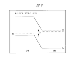
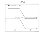
- FIG. 6 is a band diagram when a forward bias larger than a predetermined voltage is applied. It is a band figure in the case where a voltage is not applied to a tunnel junction. It is a band figure at the time of applying the forward bias below a predetermined voltage.
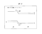
- FIG. 6 is a band diagram when a forward bias larger than a predetermined voltage is applied. It is a graph which shows the impurity profile of a p-type semiconductor region and an n-type semiconductor region.
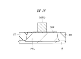
- 7 is a cross-sectional view showing a manufacturing step of the semiconductor device in the first embodiment.
- FIG. FIG. 15 is a cross-sectional view showing a manufacturing step of the semiconductor device following that of FIG.
- FIG. 16 is a cross-sectional view showing a manufacturing step of the semiconductor device following that of FIG. 15;
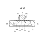
- FIG. 17 is a cross-sectional view showing a manufacturing step of the semiconductor device following that of FIG. 16;
- FIG. 18 is a cross-sectional view showing a manufacturing step of the semiconductor device following that of FIG. 17;
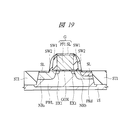
- FIG. 19 is a cross-sectional view showing the manufacturing process of the semiconductor device, following FIG. 18;
- FIG. 6 is a circuit diagram showing an inverter circuit in a second embodiment. It is sectional drawing which shows the device structure of an n channel type semiconductor element and a p channel type semiconductor element.
- FIG. 11 is a cross-sectional view showing a manufacturing step of the semiconductor device in the second embodiment.
- FIG. 23 is a cross-sectional view showing a manufacturing step of the semiconductor device following that of FIG. 22;
- FIG. 24 is a cross-sectional view showing the manufacturing process of the semiconductor device, following FIG. 23;
- FIG. 25 is a cross-sectional view showing the manufacturing process of the semiconductor device, following FIG. 24;
- FIG. 26 is a cross-sectional view showing a manufacturing step of the semiconductor device following that of FIG. 25;
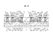
- FIG. 27 is a cross-sectional view showing a manufacturing step of the semiconductor device following that of FIG. 26;
- FIG. 6 is a cross-sectional view showing a device structure of a semiconductor device in a third embodiment.
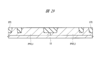
- FIG. 11 is a cross-sectional view showing a manufacturing step of the semiconductor device in the third embodiment.
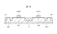
- FIG. 30 is a cross-sectional view showing a manufacturing step of the semiconductor device following that of FIG. 29;
- FIG. 31 is a cross-sectional view showing a manufacturing step of the semiconductor device following that of FIG. 30;
- FIG. 32 is a cross-sectional view showing the manufacturing process of the semiconductor device, following FIG. 31;
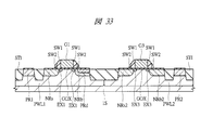
- FIG. 33 is a cross-sectional view showing a manufacturing step of the semiconductor device following that of FIG. 32;
- FIG. 34 is a cross-sectional view showing the manufacturing process of the semiconductor device, following FIG. 33;
- It is a circuit diagram which shows the example which comprises an SRAM cell combining two single transistors and two n channel type semiconductor elements.
- FIG. 31 is a cross-sectional view showing a manufacturing step of the semiconductor device following that of FIG. 30;
- FIG. 32 is a cross-sectional view showing the manufacturing process of the semiconductor device, following FIG. 31;
- FIG. 33 is a cross-sectional view showing a manufacturing step of the semiconductor device following that of FIG
- FIG. 5 is a circuit diagram showing an example in which an SRAM cell is configured by combining two single transistors, two n-channel semiconductor elements, and two p-channel semiconductor elements. It is the top view which looked at the semiconductor element in Embodiment 4 from the upper part.
- FIG. 38 is a cross-sectional view taken along line X2-X2 of FIG.
- FIG. 10 is a cross-sectional view showing a manufacturing step of the semiconductor device in the fourth embodiment.
- FIG. 40 is a cross-sectional view showing the manufacturing process of the semiconductor device, following FIG. 39;
- FIG. 41 is a cross-sectional view showing a manufacturing step of the semiconductor device following that of FIG. 40;
- FIG. 42 is a cross-sectional view showing a manufacturing step of the semiconductor device following that of FIG. 41;
- FIG. 40 is a cross-sectional view showing the manufacturing process of the semiconductor device, following FIG. 39;
- FIG. 41 is a cross-sectional view showing a manufacturing step of the semiconductor device following that of
- FIG. 43 is a cross-sectional view showing a manufacturing step of the semiconductor device following that of FIG. 42;
- FIG. 44 is a cross-sectional view showing the manufacturing process of the semiconductor device, following FIG. 43;
- FIG. 45 is a cross-sectional view showing the manufacturing process of the semiconductor device, following FIG. 44;
- It is sectional drawing which shows the modification 1.
- FIG. It is sectional drawing which shows the structural example which makes a buried insulating layer thin.
- it is a graph which shows the result of having measured the potential change in the node at the time of applying a voltage to a gate electrode. For example, it is a graph showing drain current-gate voltage characteristics of a semiconductor element when a relatively high potential of 0.8 V is applied to the drain terminal.
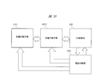
- FIG. 10 is a circuit block diagram of a semiconductor chip in a fifth embodiment.
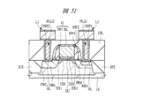
- FIG. 10 is a cross-sectional view showing a device structure of a nonvolatile memory cell in a sixth embodiment.
- the constituent elements are not necessarily indispensable unless otherwise specified and apparently essential in principle. Needless to say.
- a tunnel bipolar transistor is a bipolar transistor having a tunnel junction between an emitter and a base.
- the problem of integration does not occur. That is, in the planar technology, the drain region (drain diffusion layer) and the source region (source diffusion layer) of the MOSFET are formed in a self-aligned manner by using an ion implantation method with respect to the gate electrode.
- the gate electrode is formed small, the drain region and the source region that determine the element characteristics in accordance with the gate electrode can be formed extremely small (close to each other). As a result, the overall performance can be reduced while improving the device performance, which is a factor that can enhance the integration.
- the tunnel diode of the present invention can be formed in a self-aligned manner with respect to the gate electrode. Therefore, it is clear that the structure of the present invention does not cause the problem of integration.
- FIG. 1 is an equivalent circuit diagram of the semiconductor element according to the first embodiment.
- the semiconductor element in the first embodiment is a single element in structure, it is considered to include a MOSFET and a tunnel bipolar transistor in terms of an equivalent circuit by incorporating a tunnel diode in the drain region (drain diffusion layer). be able to.
- tunnel bipolar transistors have not been common so far, there is no equivalent circuit symbol widely used. Therefore, in this specification, it will be learned to represent a junction with a normal arrow, imitating a bipolar transistor, and will be described using a rectangular symbol for the junction.
- the notation with an arrow includes the meaning of the N / P junction, but the rectangular symbol here simply represents the junction position.
- an n-channel MOSFET is used as the MOSFET
- a PNP tunnel bipolar transistor is used as the tunnel bipolar transistor.
- the semiconductor element in the first embodiment has a MOSFET and a tunnel bipolar transistor.
- the source region of the MOSFET is connected to the source terminal S, and the gate electrode of the MOSFET is connected to the gate terminal GT.
- the drain region of the MOSFET is connected to the base region of the tunnel bipolar transistor, and this connection region is expressed as a node A.
- the emitter region of the tunnel bipolar transistor is connected to the drain terminal D, and the collector region of the tunnel bipolar transistor is connected to the substrate terminal Sub.
- the junction between the emitter region and the base region is a tunnel junction, which is represented by a rectangular symbol in FIG.
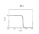
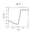
- FIG. 2 is a graph showing a result of measuring a potential ( ⁇ n) change at the node A when a voltage is applied to the gate electrode.
- the drain terminal of the drain potential V D is applied to the D
- the Yuku raising the gate potential V G applied to the gate terminal GT contrary to the potential of the node A (.phi.n) the gate potential V G a
- the connection between the MOSFET and the tunnel diode surrounded by the broken line B shown in FIG. 1 forms an inverter.
- the node A which is a connection region between the MOSFET and the tunnel diode, is considered to be connected in terms of a circuit, the source terminal S and the channel resistance of the MOSFET, and the drain terminal D and the tunnel resistance of the tunnel diode. be able to. Therefore, the potential of the node A appears as a potential obtained by dividing the voltage between the source potential V S applied to the source terminal S and the drain potential V D applied to the drain terminal D by channel resistance and tunnel resistance. become. For this reason, for example, in a state where the channel of the MOSFET is turned off, the channel resistance is much higher than the tunnel resistance, so that the potential of the node A is almost the same as the drain potential V D.
- a voltage of V D ⁇ n is applied to the tunnel diode formed between the emitter region and the base region of the tunnel bipolar transistor. That is, when gradually increasing the gate voltage V G applied to the gate terminal GT, for a constant drain voltage V D, as shown in FIG. 2, the potential ⁇ n changes abruptly. For this reason, a large voltage is applied to the tunnel diode very rapidly. As a result, in the tunnel bipolar transistor, a sudden injection of charges (holes) from the emitter region toward the base region occurs due to the tunnel effect, and most of the charges (holes) injected into the base region are a semiconductor substrate (substrate Terminal Sub) will be reached.
- a rapidly increasing current can be obtained at the drain terminal D. That is, as in the semiconductor element in the first embodiment, by combining a MOSFET and a tunnel bipolar transistor, a large current that cannot be obtained by a single MOSFET can be obtained.
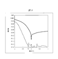
- FIG. 3 is a graph showing the drain current-gate voltage characteristics of the semiconductor element according to the first embodiment. The measurement was performed by setting the drain potential V D to 0.6V, and the source potential V S and the substrate potential V sub to 0V.
- the curve indicated by the solid line is the drain current-gate voltage characteristic of the semiconductor element in the first embodiment
- the curve indicated by the broken line is the subthreshold of the normal MOSFET alone shown for comparison. It is a characteristic.
- the slope is steeper than 60 mV / digit, which is the theoretical limit of a single MOSFET. That is, according to the first embodiment, it is possible to provide a semiconductor element having superior switching characteristics as compared with a single MOSFET, that is, having an S value smaller than 60 mV at room temperature.
- the gate potential V G rising of the drain current it will depend on the threshold voltage of the MOSFET. Therefore, the rising position of the drain current can be easily adjusted by a normal method such as ion implantation. According to the semiconductor element in the first embodiment, since an S value smaller than 60 mV can be obtained, a semiconductor element having excellent switching characteristics can be realized.
- the semiconductor element in the first embodiment has a configuration in which a MOSFET and a tunnel bipolar transistor are connected by a connection method known as Darlington connection. It has been widely used to connect a MOSFET and a normal bipolar transistor. This is because, by adopting this configuration, it is possible to combine the good responsiveness of the gate input, which is an advantage of the MOSFET, and the high current driving capability, which is an advantage of the bipolar transistor.
- bipolar transistors so far have an injection barrier due to a built-in potential of a PN junction formed between an emitter region and a base region, and thus the bipolar transistor cannot be turned on at a low voltage.
- a tunnel bipolar transistor having a tunnel junction it is possible to cause a larger change in the drain current with respect to the input (gate voltage V G ) to the gate electrode of the MOSFET. Since this tunnel bipolar transistor can be driven at a low voltage, the semiconductor device according to the first embodiment can obtain excellent switching characteristics even at a low voltage.
- a forward bias is applied to the pn junction due to the built-in potential of the pn junction formed in the boundary region between the emitter region and the base region, the voltage is less than a predetermined voltage (rising voltage).
- a predetermined voltage for example, a MOSFET and a normal bipolar transistor are combined as shown in FIG. At this time, consider a case where, for example, 0.3 V is applied to the drain terminal D and 0 V is applied to the source terminal S due to lowering of the power supply voltage.
- the pn junction formed in the boundary region between the emitter region and the base region is a tunnel junction.
- This tunnel junction also has a built-in potential, but a current (tunnel current) flows by band-to-band tunneling. That is, in the tunnel junction, when a forward bias is applied to the tunnel junction, a current caused by band-to-band tunneling flows even with a forward bias of a predetermined voltage or less.
- a forward bias of 0.3V is applied between the emitter and base regions of the tunnel bipolar transistor. That is, a forward bias of 0.3 V is applied to the tunnel junction formed in the boundary region between the emitter region and the base region.
- a tunnel current due to band-to-band tunneling flows even if the voltage is not higher than a predetermined voltage (0.3 V) at which current does not flow due to built-in potential in a normal pn junction.
- the MOSFET on by applying a threshold voltage or more gate voltage V G to turn on the MOSFET, the emitter region and the base is turned on even tunnel bipolar transistor A current flows between the regions, and a large drain current can be secured.
- the semiconductor element in the first embodiment the large drain current that cannot be secured by the MOSFET alone can be obtained by the amplification function of the tunnel bipolar transistor, and thus the theoretical limit of the conventional MOSFET alone can be obtained.
- a drain current-gate voltage characteristic having a steeper slope than 60 mV / digit can be obtained. That is, according to the first embodiment, it is possible to provide a semiconductor element having superior switching characteristics as compared with a single MOSFET, that is, having an S value smaller than 60 mV at room temperature.
- the tunnel bipolar transistor in the current amplifying function of the tunnel bipolar transistor as a bipolar transistor and in the tunnel junction formed in the boundary region between the emitter region and the base region, even if the forward bias is low voltage, even if the forward bias is low voltage, By utilizing the characteristic that a tunnel current flows by tunneling, a semiconductor element having an S value smaller than 60 mV at room temperature can be realized even at a low operating voltage.
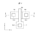
- FIG. 4 is a plan view of the semiconductor element according to the first embodiment viewed from above.
- an n-type semiconductor region NRs and an n-type semiconductor region NRb are formed so as to be spaced apart in the X direction.
- a p-type semiconductor region PRd is formed above the n-type semiconductor region NRb.
- a plug PLG1 is formed so as to be electrically connected to the p-type semiconductor region PRd, and a plug PLG2 is formed so as to be electrically connected to the n-type semiconductor region NRs.
- the gate electrode G is formed so as to extend in the Y direction between the n-type semiconductor region NRs and the semiconductor region NRb that are spaced apart.
- the gate electrode G is electrically connected to the plug PLG3 at one end of the gate electrode G.
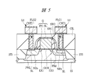
- FIG. 5 is a cross-sectional view taken along line X1-X1 of FIG.
- the semiconductor element according to the first embodiment is formed in an active region partitioned by an element isolation region STI formed in a semiconductor substrate 1S.
- a p-type well PWL into which a p-type impurity such as boron is introduced is formed in the semiconductor substrate 1S partitioned by the element isolation region STI, and is separated from the p-type well PWL.
- a pair of low-concentration n-type semiconductor regions EX1 is formed.
- the low-concentration n-type semiconductor region EX1 is a semiconductor region into which an n-type impurity such as phosphorus is introduced, and a region in the p-type well PWL sandwiched between a pair of low-concentration n-type semiconductor regions EX1 serves as a channel region.
- An n-type semiconductor region NRs and an n-type semiconductor region NRb are formed outside the low-concentration n-type semiconductor region EX1.
- the n-type semiconductor region NRs is formed further to the left of the left-side low-concentration n-type semiconductor region EX1 in the pair of low-concentration n-type semiconductor regions EX1, and the right-side low concentration in the pair of low-concentration n-type semiconductor regions EX1
- An n-type semiconductor region NRb is formed on the right side of the n-type semiconductor region EX1.
- the n-type semiconductor region NRs and the n-type semiconductor region NRb are semiconductor regions into which an n-type impurity such as arsenic is introduced.
- the p-type semiconductor region PRd is formed so as to be included in the n-type semiconductor region NRb.
- the p-type semiconductor region PRd is a semiconductor region into which a p-type impurity such as boron is introduced.
- a gate insulating film GOX is formed on the channel region, and a gate electrode G is formed on the gate insulating film GOX.
- the gate insulating film GOX is formed of, for example, a silicon oxide film, but is not limited thereto, and may be formed of, for example, a high dielectric constant film having a higher dielectric constant than a silicon oxide film such as a hafnium oxide film.
- the gate electrode G is formed of, for example, a polysilicon film PF1 (n-type polysilicon film) into which phosphorus is introduced and a silicide film SL formed on the polysilicon film PF1.
- the silicide film SL is a film formed for reducing the resistance of the gate electrode G.
- the silicide film SL is, for example, a cobalt silicide film, a titanium silicide film, a nickel silicide film, a platinum silicide film, or a nickel platinum silicide. It is formed from a film or the like.
- a side wall SW1 is formed on both side walls of the gate electrode G, and a side wall SW2 is formed outside the side wall SW1.
- a silicide film SL is formed in a region outside the sidewall SW2. Specifically, the silicide film SL is formed on the surface of the n-type semiconductor region NRs exposed outside the left sidewall SW2, and the p-type semiconductor region exposed outside the right sidewall SW2.
- a silicide film SL is also formed on the surface of PRd.
- the semiconductor element in the first embodiment is configured as described above, and this semiconductor element includes a MOSFET and a tunnel bipolar transistor. That is, the low-concentration n-type semiconductor region EX1, the n-type semiconductor region NRs, and the silicide film SL on the left side form a MOSFET source region.
- the gate insulating film GOX formed on the channel region constitutes the gate insulating film of the MOSFET, and the gate electrode G formed on the gate insulating film GOX constitutes the gate electrode of the MOSFET.
- the low-concentration n-type semiconductor region EX1 and the n-type semiconductor region NRb on the right side form a connection region (MOSFET drain region) between the MOSFET and the tunnel bipolar transistor.
- the p-type semiconductor region PRd and the silicide film SL are the emitter regions of the tunnel bipolar transistor, and the low-concentration n-type semiconductor region EX1 and the n-type semiconductor region NRb on the right side are the base regions of the tunnel bipolar transistor. .
- the p-type well PWL and the semiconductor substrate 1S are the collector region of the tunnel bipolar transistor.
- the semiconductor element in the first embodiment includes a MOSFET and a tunnel bipolar transistor, and the MOSFET and the tunnel bipolar transistor are electrically connected such that the drain region of the MOSFET becomes the base region of the tunnel bipolar transistor. It can be seen that they are configured.
- a contact interlayer insulating film CIL made of a silicon oxide film using TEOS as a raw material is formed on the semiconductor substrate 1S covering the thus configured semiconductor element.
- a contact hole CNT1 is formed so as to penetrate through the contact interlayer insulating film CIL and reach the silicide film SL formed on the surface of the p-type semiconductor region PRd.
- a contact hole CNT2 is formed so as to penetrate the contact interlayer insulating film CIL and reach the silicide film SL formed on the surface of the n-type semiconductor region NRs.
- the contact hole CNT1 and the contact hole CNT2 are filled with a titanium / titanium nitride film serving as a barrier conductor film and a tungsten film formed on the barrier conductor film to form plugs PLG1 and PLG2. ing.
- a wiring L1 is formed on the contact interlayer insulating film CIL in which the plug PLG1 and the plug PLG2 are formed.
- the wiring L1 is formed of a laminated film of a titanium nitride film, an aluminum film, and a titanium nitride film.
- a feature of the semiconductor element in the first embodiment is that the p-type semiconductor region PRd is formed so as to be included in the n-type semiconductor region NRb, and the n-type semiconductor region NRb and the p-type semiconductor region PRd are separated from each other.
- the tunnel junction is formed in the boundary region between them. Thereby, for example, even when a low voltage is applied to the p-type semiconductor region PRd, a tunnel junction is formed between the p-type semiconductor region PRd and the n-type semiconductor region NRb.
- a large drain current that cannot be obtained by a single MOSFET can be obtained by the amplification function of the tunnel bipolar transistor.
- the normal bipolar transistor In order to turn on the normal bipolar transistor, a voltage equal to or higher than a predetermined voltage (rising voltage) must be applied between the emitter region and the base region.
- a predetermined voltage for example, a voltage equal to or higher than a predetermined voltage (rising voltage) must be applied between the emitter region and the base region.
- the normal bipolar transistor is used.
- a tunnel bipolar transistor is used instead of a transistor. Therefore, the tunnel bipolar transistor can be turned on even when a forward bias equal to or lower than the predetermined voltage (rising voltage) described above is applied between the emitter region and the base region of the tunnel bipolar transistor.
- the S value is reduced by combining the MOSFET and the bipolar transistor having a current amplification function.
- a semiconductor element of 60 mV or less can be obtained.
- the bipolar transistor cannot be turned on with a forward bias equal to or lower than a predetermined voltage (rising voltage), and therefore it is not possible to cope with a reduction in power supply voltage.
- the first embodiment focuses on a tunnel bipolar transistor that can be turned on with a forward bias equal to or lower than a predetermined voltage (rising voltage).
- the semiconductor device in response to the lowering of the power supply voltage, a normal bipolar transistor is not used as the bipolar transistor, but a tunnel bipolar transistor is used, thereby reducing the power supply voltage.
- the semiconductor device in response to the lowering of the power supply voltage, a normal bipolar transistor is not used as the bipolar transistor, but a tunnel bipolar transistor is used, thereby reducing the power supply voltage.
- the semiconductor device in response to the lowering of the power supply voltage, a normal bipolar transistor is not used as the bipolar transistor, but a tunnel bipolar transistor is used, thereby reducing the power supply voltage.
- the semiconductor device can be turned on, and as a result, a semiconductor device having a low voltage operation and an S value of 60 mV / digit or less can be obtained.
- FIG. 6 is a graph showing the relationship between the voltage applied to the junction and the absolute value of the current flowing through the junction, where the solid line indicates the tunnel junction in the first embodiment and the broken line indicates a normal pn junction.
- the horizontal axis represents the voltage applied to the junction. At this time, the voltage in the positive direction indicates that a reverse bias is applied to the junction, and the voltage in the negative direction indicates that a forward bias is applied to the junction.
- the vertical axis indicates the absolute value of the current flowing through the junction in a logarithmic display.
- a normal pn junction means that almost no current (reverse current) flows when a reverse bias is applied, and the forward bias is a predetermined voltage (rising voltage) even when a forward bias is applied. It can be defined as a junction having a characteristic that current does not flow when it is equal to or less than (Vf), and current (forward current) flows only when the forward bias exceeds a predetermined voltage (Vf).
- the characteristics of the tunnel junction in the first embodiment indicated by the solid line will be described.
- the current value is suppressed to 1 ⁇ 10 ⁇ 9 (1E-09) A or less even when the reverse bias is increased. Recognize.
- the reverse current tends to increase compared to the normal pn junction indicated by the broken line, but the current value is still kept below a certain value even if the reverse bias is increased. Therefore, it can be seen that this tunnel junction also has a constant current suppressing function (rectifying function) against the reverse bias.
- rectifying function rectifying function
- a current (forward current) suddenly flows when the forward bias is greater than 0V. That is, it can be seen that a current (forward current) flows in the tunnel junction even when a forward bias of a predetermined voltage or less is applied. That is, in the normal pn junction, when the forward bias is equal to or lower than the predetermined voltage (Vf), current (forward current) hardly flows, whereas in the tunnel junction, the forward bias is equal to or lower than the predetermined voltage (Vf). Even in this case, it is greatly different that a large current (forward current) flows.
- the tunnel junction in the first embodiment is that, even when a forward bias of a predetermined voltage (Vf) or less is applied in the forward direction, almost no current flows, but a forward current flows,
- Vf predetermined voltage
- it can be defined as a junction having a constant current suppression function when a reverse bias is applied.
- the left region of FIG. 7 shows a p-type semiconductor region, and the right region of FIG. 7 shows an n-type semiconductor region.
- the Fermi level Ef of the p-type semiconductor region is The Fermi level Ef of the n-type semiconductor region that exists immediately above the electron band Ev exists immediately below the conduction band Ec.
- the Fermi level Ef of the p-type semiconductor region and the Fermi level Ef of the n-type semiconductor region coincide with each other. Therefore, as shown in FIG. There will be potential.
- FIG. 8 is a band diagram when a forward bias (
- V a forward bias of a predetermined voltage
- Vf a potential difference
- is generated between the Fermi level Ef of the p-type semiconductor region and the Fermi level Ef of the n-type semiconductor region.
- V the built-in potential becomes smaller than the built-in potential in the equilibrium state.
- the magnitude of the built-in potential is still large, electrons in the conduction band Ec of the n-type semiconductor region can overcome the built-in potential and diffuse into the conduction band Ec of the p-type semiconductor region.
- FIG. 9 is a band diagram when a forward bias (
- Vf a forward bias larger than a predetermined voltage
- the left region of FIG. 10 shows a p-type semiconductor region, and the right region of FIG. 10 shows an n-type semiconductor region.
- the Fermi level Ef of the p-type semiconductor region is the valence band.
- the Fermi level Ef of the n-type semiconductor region enters the inside of the conduction band Ec.
- FIG. 11 is a band diagram when a forward bias (
- V a potential difference
- is generated between the Fermi level Ef of the p-type semiconductor region and the Fermi level Ef of the n-type semiconductor region.
- V the Fermi level Ef of the p-type semiconductor region
- the Fermi level Ef of the n-type semiconductor region enters the conduction band Ec.
- an overlap occurs between the valence band Ev of the p-type semiconductor region and the conduction band Ec of the n-type semiconductor region. That is, the empty level existing in the p-type semiconductor region and the filled level existing in the n-type semiconductor region are opposed at the same energy level.
- the tunnel junction since the impurity concentration in the p-type semiconductor region and the impurity concentration in the n-type semiconductor region are high enough to degenerate, the depletion layer formed in the tunnel junction becomes very narrow, and the tunnel junction The electric field at the junction is extremely large.
- holes existing in the p-type semiconductor region move (tunnel) by band-to-band tunneling from the valence band Ev of the p-type semiconductor region to the conduction band Ec of the n-type semiconductor region.
- electrons existing in the n-type semiconductor region move (tunnel) by band-to-band tunneling from the conduction band Ec of the n-type semiconductor region to the valence band Ev of the p-type semiconductor region.
- a current (forward current) due to band-to-band tunneling flows in the tunnel junction even when a forward bias (
- FIG. 12 is a band diagram when a forward bias (
- Vf a forward bias larger than a predetermined voltage
- the junction formed in the boundary region between the p-type semiconductor region PRd and the n-type semiconductor region NRb is formed by the tunnel junction described above.
- the impurity concentration of the p-type semiconductor region PRd and the impurity concentration of the n-type semiconductor region NRb need to be high enough to degenerate.
- the impurity concentration of the n-type semiconductor region NRb needs to be as low as possible while being degenerate. The reason for this will be described.
- the semiconductor element according to the first embodiment is a tunnel having a p-type semiconductor region PRd as an emitter region, an n-type semiconductor region NRb as a base region, and a p-type well PWL (semiconductor substrate 1S) as a collector region.
- a tunnel junction is formed between the p-type semiconductor region PRd as the emitter region and the n-type semiconductor region NRb as the base region, and a forward bias is applied between the emitter region and the base region of the tunnel bipolar transistor. Then, an emitter current flows from the emitter region to the base region.
- This emitter current is a current due to band-to-band tunneling at the tunnel junction, and a hole current flowing from the emitter region (p-type semiconductor region PRd) to the base region (n-type semiconductor region NRb) and the base region (n-type semiconductor region). NRb) to an emitter region (p-type semiconductor region PRd).
- the emitter current is a hole current. That is, most of the hole current injected from the emitter region to the base region is extracted to the collector region, so that the amplification operation of the tunnel bipolar transistor is performed, while the electron current injected from the base region to the emitter region is the tunnel bipolar transistor. It does not contribute to the amplification operation of the transistor. Therefore, increasing the hole current flowing from the emitter region to the base region and reducing the electron current flowing from the base region to the emitter region as much as possible can improve the amplification factor of the tunnel bipolar transistor. This means that it is desirable that the emitter injection efficiency (hole current / (hole current + electron current)) be as close to 1 as possible.
- the emitter injection efficiency can be improved by lowering the impurity concentration of the base region and increasing the impurity concentration of the emitter region. Therefore, since the junction formed at the boundary region between the p-type semiconductor region PRd and the n-type semiconductor region NRb needs to be formed as a tunnel junction, the impurity concentration of the n-type semiconductor region NRb serving as the base region is high enough to degenerate. On the other hand, when considered as a tunnel bipolar transistor, it is desirable that the impurity concentration of the n-type semiconductor region NRb serving as the base region be lowered.
- the impurity concentration of the n-type semiconductor region NRb is as low as possible while being degenerate.
- the impurity concentration of the n-type semiconductor region NRb serving as the base region is set lower than the impurity concentration of the p-type semiconductor region PRd serving as the emitter region.
- the impurity concentration of the p-type semiconductor region PRd is set to the order of 10 20 / cm 3
- the impurity concentration of the n-type semiconductor region NRb is set to the order of 10 19 / cm 3 .
- FIG. 13 is a graph showing impurity profiles of the p-type semiconductor region PRd and the n-type semiconductor region NRb.
- the horizontal axis indicates the depth from the semiconductor substrate (substrate depth), and the vertical axis indicates the impurity concentration.
- the p-type semiconductor region PRd is formed over a depth of about 0 nm to 15 nm, and the impurity concentration (boron concentration) peak of the p-type semiconductor region PRd is on the order of 10 20 / cm 3 . It has become.
- the n-type semiconductor region NRb is formed over a depth of about 0 nm to 25 nm, and the peak of the impurity concentration (arsenic concentration) of the n-type semiconductor region NRb is on the order of 10 19 / cm 3 .
- a tunnel junction is formed by the p-type semiconductor region PRd and the n-type semiconductor region NRb, and the n-type semiconductor region NRb has a higher impurity concentration than the p-type semiconductor region PRd.
- the p-type semiconductor region PRd and the n-type semiconductor region NRb are degenerated so that even when a forward bias of a predetermined voltage (Vf) or less is applied in the forward direction, the interband tunneling is performed. It has a characteristic that a forward current flows.
- Vf predetermined voltage
- the configuration in which the impurity concentration of the n-type semiconductor region NRb is lower than the impurity concentration of the p-type semiconductor region PRd improves the emitter injection efficiency from the viewpoint of the tunnel bipolar transistor. It can be said that it is made for that purpose.
- the impurity concentration of the n-type semiconductor region NRb is as low as possible, the depletion layer extends when a reverse bias is applied.
- the interband tunneling at the time of application is suppressed and the reverse current is suppressed. Therefore, in the tunnel junction according to the first embodiment, even when a forward bias of a predetermined voltage (Vf) or less is applied in the forward direction, almost no current flows but a forward current flows and the reverse bias is applied. It can be said that this is a junction having a constant current suppressing function when a voltage is applied.
- Vf predetermined voltage
- a technique for forming a heterostructure using germanium or silicon / germanium crystals having a narrow band gap is known, and this technique can also be applied to the first embodiment. .
- a 10 nm silicon oxide film for example, is formed on the surface of a semiconductor substrate (p-type silicon substrate) 1S by a thermal oxidation method, and then a 100 nm silicon nitride film is formed by CVD (Chemical Vapor Deposition). Deposit using the method. Then, the active region is patterned using a photolithography technique. Thereafter, by using dry etching technology, the silicon nitride film and the silicon oxide film are anisotropically etched in a direction perpendicular to the main surface (substrate surface) of the semiconductor substrate 1S, and then the semiconductor substrate 1S is anisotropically processed. Etching is performed to form, for example, a trench having a depth of 300 nm in the semiconductor substrate 1S.
- the silicon surface exposed inside the trench is oxidized to form a 5 nm silicon oxide film, and further a 700 nm silicon oxide film is deposited on the semiconductor substrate 1S by the CVD method.
- the CVD method by using a CMP (Chemical-Mechanical-Polishing) method, the deposited silicon oxide film is polished using the silicon nitride film as a base mask, and the silicon oxide deposited on the semiconductor substrate 1S is removed except for the inside of the trench. Remove the membrane. Thereafter, the silicon nitride film used as the mask is removed by wet etching with hot phosphoric acid.
- the element isolation region STI can be formed on the main surface side of the semiconductor substrate 1S.
- the impurity concentration near the substrate surface is 8 ⁇ 10 17 / cm.
- a p-type well PWL set to ⁇ 3 is formed.
- the threshold value of the MOSFET can be adjusted by setting the impurity concentration profile in the p-type well PWL.
- a gate insulating film GOX of, for example, 3 nm is formed in the active region by using a thermal oxidation method.
- the gate insulating film GOX is formed from, for example, a silicon oxide film, but is not limited thereto, and may be formed from a high dielectric constant film having a dielectric constant higher than that of the silicon oxide film.
- a polysilicon film PF1 is deposited on the gate insulating film GOX with a thickness of about 100 nm by using the CVD method. At this time, the polysilicon film PF1 is doped with phosphorus at a high concentration by using an in-situ doping method or an ion implantation method.
- the polysilicon film PF1 is patterned by using a photolithography technique and a dry etching method. Specifically, the resist film formed on the polysilicon film PF1 is patterned using a photolithography technique. Then, the polysilicon film PF1 is dry-etched using the patterned resist film as a mask. Thus, the gate electrode G made of the polysilicon film PF1 is formed by anisotropically etching the polysilicon film PF1 in the direction perpendicular to the substrate surface of the semiconductor substrate 1S.
- a low concentration n-type semiconductor region EX1 aligned with the gate electrode G is formed in the semiconductor substrate 1S by using a photolithography technique and an ion implantation method.
- a silicon oxide film is deposited to a thickness of about 50 nm on the semiconductor substrate 1S covering the gate electrode G by CVD, and the deposited silicon oxide film is anisotropically etched.
- the sidewall SW1 is formed on the sidewalls on both sides of the gate electrode G.
- arsenic is doped in the semiconductor substrate 1S with an acceleration energy of 25 keV and a dose of about 5 ⁇ 10 14 / cm 2 by an ion implantation method using the gate electrode G on which the sidewall SW1 is formed as a mask.
- the n-type semiconductor region NRs and the n-type semiconductor region NRb can be formed.
- the impurity (arsenic) introduced by the heat treatment may be activated.
- the resist film can be patterned together with the gate electrode G on which the sidewall SW1 is formed to form a mask for the ion implantation method.
- the n-type semiconductor region NRs and the n-type semiconductor region NRb can have different impurity concentrations.
- a silicon oxide film is deposited to a thickness of about 50 nm on the semiconductor substrate 1S covering the gate electrode G by the CVD method.
- the side wall SW2 is formed outside the side wall SW1 by anisotropically etching the deposited silicon oxide film.
- the p-type semiconductor region PRd is formed so as to be included in the n-type semiconductor region NRb.
- boron (B) which is a p-type impurity is doped with an acceleration energy of 2 keV and a dose amount of about 2 ⁇ 10 15 / cm 2 .
- n-type semiconductor region NRb and the p-type semiconductor region PRd are formed to have an impurity profile as shown in FIG.
- a tunnel junction can be formed in the boundary region between the n-type semiconductor region NRb and the p-type semiconductor region PRd.
- the p-type semiconductor region PRd can be formed in the n-type semiconductor region NRb in a self-aligning manner. Since the p-type semiconductor region PRd is formed so as to be included in the n-type semiconductor region NRb, even if a new p-type semiconductor region PRd is formed, the size of the semiconductor element in the first embodiment is as follows. It can be formed in the same size as that of a single MOSFET. For this reason, the semiconductor element according to the first embodiment has an advantage that it can be formed with the same degree of integration as a single MOSFET without affecting the degree of integration.
- the semiconductor element according to the first embodiment even if a positive voltage (for example, 0.6 V) is applied to the drain region which is the p-type semiconductor region PRd, the conductivity opposite to that of the p-type well PWL (semiconductor substrate 1S). Since only the n-type semiconductor region NRb, which is a type, is in contact with the semiconductor substrate 1S, there is no leakage current due to forward bias. Further, the characteristics of the tunnel junction formed by the p-type semiconductor region PRd and the n-type semiconductor region NRb can be changed by adjusting the implantation energy of the impurities implanted into the p-type semiconductor region PRd and the n-type semiconductor region NRb. Can do.
- a positive voltage for example, 0.6 V
- the extraction of charges (holes) injected into the n-type semiconductor region NRb from the p-type semiconductor region PRd into the semiconductor substrate 1S is a longitudinal impurity distribution of the p-type semiconductor region PRd and the n-type semiconductor region NRb, that is, Along with the effective thickness of the n-type semiconductor region NRb (base region), the lateral width, that is, the width of the sidewall SW2, and the impurity profile of the channel region can be controlled.
- the extraction efficiency can be improved by reducing the width of the n-type semiconductor region NRb (base region).
- the leakage current can be reduced by increasing the width of the n-type semiconductor region NRb (base region).
- the extraction efficiency can be improved by reducing the width of the sidewall SW2, and the extraction efficiency can be improved by increasing the impurity concentration of the channel region.
- a silicide film SL is selectively formed on the upper surface of the gate electrode G, the surface of the p-type semiconductor region PRd, and the surface of the n-type semiconductor region NRs using the sidewall SW2 as a mask. To do. Thereby, the resistance of the gate electrode G, the p-type semiconductor region PRd, and the n-type semiconductor region NRs can be reduced. This is a normal process known as the salicide process.
- the silicide film SL can be formed of, for example, a cobalt silicide film, a titanium silicide film, a nickel silicide film, a platinum silicide film, or a nickel platinum silicide film.
- the semiconductor element in the first embodiment can be obtained by performing a wiring process used in a normal LSI.
- a contact interlayer insulating film CIL made of, for example, a silicon oxide film is formed on the semiconductor substrate 1S, and the surface thereof is planarized by CMP. Then, by using a photolithography technique and an etching technique, contact holes CNT1 and CNT2 penetrating through the contact interlayer insulating film CIL are formed.
- a titanium / titanium nitride film is formed on the contact interlayer insulating film CIL including the bottom and inner walls of the contact holes CNT1 and CNT2.
- the titanium / titanium nitride film is composed of a laminated film of a titanium film and a titanium nitride film, and can be formed by using, for example, a sputtering method.
- This titanium / titanium nitride film has a so-called barrier property that prevents, for example, tungsten, which is a material of a film to be embedded in a later process, from diffusing into silicon.
- a tungsten film is formed on the entire main surface of the semiconductor substrate 1S so as to fill the contact holes CNT1 and CNT2.
- This tungsten film can be formed using, for example, a CVD method.
- the unnecessary plugs PLG1 and PLG2 can be formed by removing unnecessary titanium / titanium nitride films and tungsten films formed on the contact interlayer insulating film CIL by, for example, CMP.
- a titanium / titanium nitride film, an aluminum film, and a titanium / titanium nitride film are sequentially formed on the contact interlayer insulating film CIL and the plugs PLG1 and PLG2.
- These films can be formed by using, for example, a sputtering method.
- the wiring L1 can be formed by patterning these films.
- the resistance reduction process etc. which are known until now can be used for these wiring processes.
- the wiring L1 formed in the wiring process described above is an aluminum wiring
- the wiring L1 can be formed from a copper wiring (damascene wiring).
- multilayer wiring can be formed as necessary.
- the semiconductor device according to the first embodiment can be manufactured. It is obvious that the semiconductor element formed by the manufacturing process described above can be manufactured with the same planar layout as a normal MOSFET. For this reason, according to the semiconductor device in this Embodiment 1, a high-performance semiconductor device can be obtained without impairing the integration.
- FIG. 1 showing an equivalent circuit of the semiconductor element in the first embodiment
- the source terminal S and the substrate terminal Sub are shown separately for the sake of explanation, but the source potential is shown. Since both V s and substrate potential V sub are set to 0 V, a three-terminal element can be formed by connecting both terminals. Further, considering that the injected charge is extracted from the n-type semiconductor region NRb to the semiconductor substrate 1S, the substrate potential V sub is set lower than the source potential V s , and the reverse is between the n-type semiconductor region NRb and the semiconductor substrate 1S. The extraction efficiency can be improved by applying a bias.
- the n-channel type semiconductor element in which the n-channel type MOSFET and the PNP type tunnel bipolar transistor are combined has been described.
- the p-channel type MOSFET and the NPN type tunnel bipolar transistor are combined.
- a p-channel semiconductor element can also be formed. Therefore, in the semiconductor element of the present invention, a complementary semiconductor element can be formed using an n-channel semiconductor element and a p-channel semiconductor element.
- a complementary semiconductor element in which an n-channel semiconductor element and a p-channel semiconductor element are combined will be described.
- an inverter circuit will be described as an example of a circuit using complementary semiconductor elements.
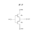
- FIG. 20 is a circuit diagram showing an inverter circuit according to the second embodiment.
- a p-channel semiconductor element PTr and an n-channel semiconductor element NTr are connected in series between a power supply potential VDD and a ground potential GND.
- a p-channel semiconductor element PTr is disposed on the power supply potential VDD side
- an n-channel semiconductor element NTr is disposed on the ground potential GND side.
- the gate electrode of the p-channel semiconductor element PTr and the gate electrode of the n-channel semiconductor element are electrically connected to form an input IN, and the drain region of the p-channel semiconductor element and the drain of the n-channel semiconductor element
- the node connecting the areas is the output OUT.
- the gate electrode of the p-channel semiconductor element PTr and the gate electrode of the n-channel semiconductor element NTr are applied. “H” is applied. In this case, the p-channel type semiconductor element PTr is turned off and the n-channel type semiconductor element NTr is turned on. Therefore, the output OUT is electrically connected to the ground potential GND by the turned-on n-channel semiconductor element NTr, and “L” (for example, 0 V) is output from the output OUT.
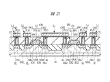
- FIG. 21 is a cross-sectional view showing device structures of an n-channel semiconductor element NTr and a p-channel semiconductor element PTr.
- an element isolation region STI is formed on the main surface side on the semiconductor substrate 1S, and a p-type well PWL and an n-type well NWL are formed in an active region (active region) partitioned by the element isolation region STI.
- a p-type well PWL is formed in the left region
- an n-type well NWL is formed in the right region.
- An n-channel semiconductor element NTr is formed on the p-type well PWL, and a p-channel semiconductor element PTr is formed on the n-type well NWL.
- n-channel semiconductor element NTr formed on the p-type well PWL will be described.
- a p-type well PWL into which a p-type impurity such as boron is introduced is formed, and a pair of low-concentrations are separated in the p-type well PWL.
- An n-type semiconductor region EX1 is formed.
- the low-concentration n-type semiconductor region EX1 is a semiconductor region into which an n-type impurity such as phosphorus is introduced, and a region in the p-type well PWL sandwiched between a pair of low-concentration n-type semiconductor regions EX1 serves as a channel region.
- An n-type semiconductor region NRs and an n-type semiconductor region NRb are formed outside the low-concentration n-type semiconductor region EX1. That is, the n-type semiconductor region NRs is formed further to the left of the left-side low-concentration n-type semiconductor region EX1 in the pair of low-concentration n-type semiconductor regions EX1, and the right-side low concentration in the pair of low-concentration n-type semiconductor regions EX1.
- An n-type semiconductor region NRb is formed on the right side of the n-type semiconductor region EX1.
- the n-type semiconductor region NRs and the n-type semiconductor region NRb are semiconductor regions into which an n-type impurity such as arsenic is introduced.
- the p-type semiconductor region PRd is formed so as to be included in the n-type semiconductor region NRb.
- the p-type semiconductor region PRd is a semiconductor region into which a p-type impurity such as boron is introduced.
- a gate insulating film GOX is formed on the channel region, and a gate electrode G1 is formed on the gate insulating film GOX.
- the gate insulating film GOX is formed of, for example, a silicon oxide film, but is not limited thereto, and may be formed of, for example, a high dielectric constant film having a higher dielectric constant than a silicon oxide film such as a hafnium oxide film.
- the gate electrode G1 is formed of, for example, a polysilicon film PF1 (n-type polysilicon film) into which phosphorus is introduced and a silicide film SL formed on the polysilicon film PF1.
- the silicide film SL is a film formed for reducing the resistance of the gate electrode G1, and the silicide film SL is, for example, a cobalt silicide film, a titanium silicide film, a nickel silicide film, a platinum silicide film, or a nickel platinum silicide. It is formed from a film or the like.
- a side wall SW1 is formed on both side walls of the gate electrode G1, and a side wall SW2 is formed outside the side wall SW1.
- a silicide film SL is formed in a region outside the sidewall SW2. Specifically, the silicide film SL is formed on the surface of the n-type semiconductor region NRs exposed outside the left sidewall SW2, and the p-type semiconductor region exposed outside the right sidewall SW2.
- a silicide film SL is also formed on the surface of PRd.
- the n-channel semiconductor element NTr in the second embodiment is configured as described above, and the n-channel semiconductor element NTr includes an n-channel MOSFET and a PNP tunnel bipolar transistor. That is, the source region of the n-channel MOSFET is formed by the low-concentration n-type semiconductor region EX1, the n-type semiconductor region NRs, and the silicide film SL on the left side.
- the gate insulating film GOX formed on the channel region constitutes the gate insulating film of the n-channel MOSFET, and the gate electrode G1 formed on the gate insulating film GOX serves as the gate electrode of the n-channel MOSFET. It is composed.
- the low-concentration n-type semiconductor region EX1 and the n-type semiconductor region NRb on the right side form a connection region between the n-channel MOSFET and the PNP tunnel bipolar transistor.
- the p-type semiconductor region PRd and the silicide film SL are the emitter regions of the PNP type tunnel bipolar transistor, and the lightly doped n-type semiconductor region EX1 and the n-type semiconductor region NRb are the base regions of the PNP type tunnel bipolar transistor. It has become.
- the p-type well PWL and the semiconductor substrate 1S are the collector regions of the PNP-type tunnel bipolar transistor.
- the n-channel semiconductor element NTr in the second embodiment includes the n-channel MOSFET and the PNP tunnel bipolar transistor, and the drain region of the n-channel MOSFET becomes the base region of the PNP tunnel bipolar transistor.
- n-channel MOSFET and the PNP tunnel bipolar transistor are electrically connected.
- a p-type power supply region PR1 for supplying a potential to the p-type well PWL is also formed in the p-type well PWL.
- an n-type well NWL into which an n-type impurity such as phosphorus or arsenic is introduced is formed in the semiconductor substrate 1S partitioned by the element isolation region STI.
- an n-type well NWL into which an n-type impurity such as phosphorus or arsenic is introduced is formed in the semiconductor substrate 1S partitioned by the element isolation region STI.
- a pair of n-type wells NWL are spaced apart from each other in the n-type well NWL.
- a low concentration p-type semiconductor region EX2 is formed.
- the low-concentration p-type semiconductor region EX2 is a semiconductor region into which a p-type impurity such as boron is introduced, and a region in the n-type well NWL sandwiched between the pair of low-concentration p-type semiconductor regions EX2 serves as a channel region.
- a p-type semiconductor region PRb and a p-type semiconductor region PRs are formed outside the low-concentration p-type semiconductor region EX2. That is, the p-type semiconductor region PRb is formed on the left side of the left-side low-concentration p-type semiconductor region EX2 in the pair of low-concentration p-type semiconductor regions EX2, and the right-side low concentration in the pair of low-concentration p-type semiconductor regions EX2.
- a p-type semiconductor region PRs is formed on the right side of the p-type semiconductor region EX2.
- the p-type semiconductor region PRb and the p-type semiconductor region PRs are semiconductor regions into which a p-type impurity such as boron is introduced.
- an n-type semiconductor region NRd is formed so as to be included in the p-type semiconductor region PRb.
- This n-type semiconductor region NRd is a semiconductor region into which an n-type impurity such as phosphorus or arsenic is introduced.
- a gate insulating film GOX is formed on the channel region, and a gate electrode G2 is formed on the gate insulating film GOX.
- the gate insulating film GOX is formed of, for example, a silicon oxide film, but is not limited thereto, and may be formed of, for example, a high dielectric constant film having a higher dielectric constant than a silicon oxide film such as a hafnium oxide film.
- the gate electrode G2 is formed of, for example, a polysilicon film PF1 (p-type polysilicon film) into which boron is introduced and a silicide film SL formed on the polysilicon film PF1.
- the silicide film SL is a film formed for reducing the resistance of the gate electrode G2.
- the silicide film SL is, for example, a cobalt silicide film, a titanium silicide film, a nickel silicide film, a platinum silicide film, or a nickel platinum silicide. It is formed from a film or the like.
- a sidewall SW1 is formed on the side walls on both sides of the gate electrode G2, and the sidewall SW2 is formed outside the sidewall SW1.
- a silicide film SL is formed in a region outside the sidewall SW2. Specifically, the silicide film SL is formed on the surface of the n-type semiconductor region NRd exposed outside the left sidewall SW2, and the p-type semiconductor region exposed outside the right sidewall SW2.
- a silicide film SL is also formed on the surface of PRs.
- the p-channel semiconductor element PTr in the second embodiment is configured as described above, and this p-channel semiconductor element PTr includes a p-channel MOSFET and an NPN tunnel bipolar transistor. That is, the source region of the p-channel MOSFET is formed by the right-side low-concentration p-type semiconductor region EX2, the p-type semiconductor region PRs, and the silicide film SL.
- the gate insulating film GOX formed on the channel region constitutes the gate insulating film of the p-channel MOSFET, and the gate electrode G2 formed on the gate insulating film GOX serves as the gate electrode of the p-channel MOSFET. It is composed.
- the low-concentration p-type semiconductor region EX2 and the p-type semiconductor region PRb on the left side form a connection region between the p-channel MOSFET and the NPN tunnel bipolar transistor.
- the n-type semiconductor region NRd and the silicide film SL are the emitter regions of the NPN tunnel bipolar transistor, and the low-concentration p-type semiconductor region EX2 and the p-type semiconductor region PRb on the left are the base regions of the NPN tunnel bipolar transistor. It has become.
- the n-type well NWL is the collector region of the NPN tunnel bipolar transistor.
- the p-channel semiconductor element PTr in the second embodiment includes the p-channel MOSFET and the NPN tunnel bipolar transistor, and the drain region of the p-channel MOSFET becomes the base region of the NPN tunnel bipolar transistor. As described above, the p-channel MOSFET and the NPN tunnel bipolar transistor are electrically connected. Note that an n-type power supply region NR1 for supplying a potential to the n-type well NWL is also formed in the n-type well NWL.
- a contact layer made of a silicon oxide film using TEOS as a raw material is formed on the semiconductor substrate 1S covering the n-channel type semiconductor element NTr and the p-channel type semiconductor element PTr configured as described above, for example, as shown in FIG. 21, a contact layer made of a silicon oxide film using TEOS as a raw material is formed.
- An insulating film CIL is formed.
- a contact hole CNT is formed so as to penetrate through the contact interlayer insulating film CIL and reach the silicide film SL.
- a titanium / titanium nitride film serving as a barrier conductor film and a tungsten film formed on the barrier conductor film are embedded to form a plug PLG.
- a wiring L1 is formed on the contact interlayer insulating film CIL in which the plug PLG is formed.
- the wiring L1 is formed of a laminated film of a titanium nitride film, an aluminum film, and a titanium nitride film.
- the semiconductor device according to the second embodiment is configured as described above, and the manufacturing method thereof will be described below with reference to the drawings.
- a 10 nm silicon oxide film is formed on the surface of a semiconductor substrate (p-type silicon substrate) 1S by a thermal oxidation method, and then a 100 nm silicon nitride film is formed by CVD (Chemical Vapor Deposition). Deposit using the method. Then, the active region is patterned using a photolithography technique. Thereafter, by using dry etching technology, the silicon nitride film and the silicon oxide film are anisotropically etched in a direction perpendicular to the main surface (substrate surface) of the semiconductor substrate 1S, and then the semiconductor substrate 1S is anisotropically processed. Etching is performed to form, for example, a trench having a depth of 300 nm in the semiconductor substrate 1S.
- the silicon surface exposed inside the trench is oxidized to form a 5 nm silicon oxide film, and further a 700 nm silicon oxide film is deposited on the semiconductor substrate 1S by the CVD method.
- the CVD method by using a CMP (Chemical-Mechanical-Polishing) method, the deposited silicon oxide film is polished using the silicon nitride film as a base mask, and the silicon oxide deposited on the semiconductor substrate 1S is removed except for the inside of the trench. Remove the membrane. Thereafter, the silicon nitride film used as the mask is removed by wet etching with hot phosphoric acid.
- the element isolation region STI can be formed on the main surface side of the semiconductor substrate 1S.
- the p-type well PWL and the n-type well NWL are formed in the semiconductor substrate 1S by using an ion implantation method and a heat treatment. Then, the surface of the semiconductor substrate 1S (silicon surface) is exposed by removing the silicon oxide film formed under the silicon nitride film with hydrofluoric acid.
- a gate insulating film GOX of, eg, 3 nm is formed in the active region by using a thermal oxidation method.
- the gate insulating film GOX is formed from, for example, a silicon oxide film, but is not limited thereto, and may be formed from a high dielectric constant film having a dielectric constant higher than that of the silicon oxide film.
- a polysilicon film PF1 is deposited on the gate insulating film GOX with a thickness of about 100 nm by using the CVD method.
- the polysilicon film PF1 formed in the n-channel type semiconductor element formation region is doped with phosphorus at a high concentration by using an ion implantation method or the like.
- the polysilicon film PF1 formed in the p-channel type semiconductor element formation region is doped with boron at a high concentration using an ion implantation method or the like.
- the polysilicon film PF1 is patterned by using a photolithography technique and a dry etching method. Specifically, the resist film formed on the polysilicon film PF1 is patterned using a photolithography technique. Then, the polysilicon film PF1 is dry-etched using the patterned resist film as a mask. As described above, the polysilicon film PF1 is anisotropically etched in the direction perpendicular to the substrate surface of the semiconductor substrate 1S, thereby forming the gate electrode G1 and the gate electrode G2 made of the polysilicon film PF1.
- a low concentration n-type semiconductor region EX1 aligned with the gate electrode G1 is formed in the semiconductor substrate 1S by using a photolithography technique and an ion implantation method.
- a low concentration p-type semiconductor region EX2 aligned with the gate electrode G2 is formed in the semiconductor substrate 1S by using a photolithography technique and an ion implantation method.
- a silicon oxide film is deposited with a thickness of about 50 nm on the semiconductor substrate 1S covering the gate electrode G1 and the gate electrode G2 by CVD, and is anisotropic to the deposited silicon oxide film. Etching is performed to form the sidewall SW1 on the sidewalls on both sides of the gate electrode G1 and the gate electrode G2.
- arsenic is doped in the p-type well PWL by an ion implantation method using the gate electrode G1 on which the sidewall SW1 is formed and the patterned resist film as a mask.
- the n-type semiconductor region NRs and the n-type semiconductor region NRb can be formed.
- an n-type power supply region NR1 is also formed in the n-type well NWL.
- boron is doped into the n-type well NWL by an ion implantation method using the gate electrode G2 on which the sidewall SW1 is formed and the patterned resist film as a mask.
- the p-type semiconductor region PRs and the p-type semiconductor region PRb can be formed.
- a p-type power supply region PR1 is also formed in the p-type well PWL.
- the impurities (arsenic and boron) introduced by the heat treatment may be activated.
- a silicon oxide film is deposited with a thickness of about 50 nm on the semiconductor substrate 1S covering the gate electrode G1 and the gate electrode G2 by a CVD method.
- the side wall SW2 is formed outside the side wall SW1 by anisotropically etching the deposited silicon oxide film.
- the p-type semiconductor region PRd is formed so as to be included in the n-type semiconductor region NRb by using a photolithography technique and an ion implantation method.
- an n-type semiconductor region NRd is formed so as to be included in the p-type semiconductor region PRb by using a photolithography technique and an ion implantation method.
- LSA Laser Spike Annealing
- the silicide film SL can be formed of, for example, a cobalt silicide film, a titanium silicide film, a nickel silicide film, a platinum silicide film, or a nickel platinum silicide film.
- the semiconductor device in the second embodiment can be obtained by performing a wiring process used in a normal LSI.
- a contact interlayer insulating film CIL made of, for example, a silicon oxide film is formed on the semiconductor substrate 1S, and the surface thereof is planarized by CMP.
- contact holes CNT penetrating through the contact interlayer insulating film CIL are formed by using a photolithography technique and an etching technique.
- a titanium / titanium nitride film is formed on the contact interlayer insulating film CIL including the bottom surface and inner wall of the contact hole CNT.
- the titanium / titanium nitride film is composed of a laminated film of a titanium film and a titanium nitride film, and can be formed by using, for example, a sputtering method.
- This titanium / titanium nitride film has a so-called barrier property that prevents, for example, tungsten, which is a material of a film to be embedded in a later process, from diffusing into silicon.
- a tungsten film is formed on the entire main surface of the semiconductor substrate 1S so as to fill the contact holes CNT.
- This tungsten film can be formed using, for example, a CVD method.
- the plug PLG can be formed by removing unnecessary titanium / titanium nitride films and tungsten films formed on the contact interlayer insulating film CIL by, for example, CMP.
- a titanium / titanium nitride film, an aluminum film, and a titanium / titanium nitride film are sequentially formed on the contact interlayer insulating film CIL and the plug PLG.
- These films can be formed by using, for example, a sputtering method.
- the wiring L1 can be formed by patterning these films.
- the resistance reduction process etc. which are known until now can be used for these wiring processes.
- the wiring L1 formed in the wiring process described above is an aluminum wiring
- the wiring L1 can be formed from a copper wiring (damascene wiring).
- multilayer wiring can be formed as necessary.
- the semiconductor device according to the second embodiment can be manufactured.
- an inverter is taken as an example.
- An inverter is a basic unit of a digital circuit, and by combining these, a basic logic circuit such as a NAND circuit, a NOR circuit, an EX-OR circuit, or a flip-flop circuit used in the digital circuit can be formed. That is, it can be seen that a digital circuit can be constructed using the n-channel semiconductor element NTr and the p-channel semiconductor element PTr in the second embodiment.
- FIG. 28 is a cross-sectional view showing the device structure of the semiconductor device according to the third embodiment.
- an element isolation region STI is formed on the main surface side on the semiconductor substrate 1S, and a p-type well PWL1 and a p-type well are formed in an active region (active region) partitioned by the element isolation region STI.
- PWL2 is formed.
- the p-type well PWL1 is formed in the left region
- the p-type well PWL2 is formed in the right region.
- An n-channel semiconductor element NTr1 is formed on the p-type well PWL1, and a single transistor NTr2 is formed on the p-type well PWL2.
- the structure of the n-channel type semiconductor element NTr1 has the same configuration as that of the n-channel type semiconductor element NTr described in the second embodiment (see FIG. 21), and the description thereof will be omitted.
- the single transistor NTr2 is a widely used single MOSFET, and this structure will be described below with reference to FIG.
- a p-type well PWL2 into which a p-type impurity such as boron is introduced is formed.
- a pair of low-concentrations are separated in the p-type well PWL2.
- An n-type semiconductor region EX3 is formed.
- the low-concentration n-type semiconductor region EX3 is a semiconductor region into which an n-type impurity such as phosphorus is introduced, and a region in the p-type well PWL2 sandwiched between the pair of low-concentration n-type semiconductor regions EX3 becomes a channel region.
- n-type semiconductor region NRs2 and an n-type semiconductor region NRb2 are formed outside the low-concentration n-type semiconductor region EX3. That is, the n-type semiconductor region NRs2 is formed on the left side of the left-side low-concentration n-type semiconductor region EX3 in the pair of low-concentration n-type semiconductor regions EX3, and the right-side low concentration in the pair of low-concentration n-type semiconductor regions EX3.
- An n-type semiconductor region NRb2 is formed on the right side of the n-type semiconductor region EX3.
- the n-type semiconductor region NRs2 and the n-type semiconductor region NRb2 are semiconductor regions into which an n-type impurity such as arsenic is introduced.
- a gate insulating film GOX is formed on the channel region, and a gate electrode G3 is formed on the gate insulating film GOX.
- the gate insulating film GOX is formed of, for example, a silicon oxide film, but is not limited thereto, and may be formed of, for example, a high dielectric constant film having a higher dielectric constant than a silicon oxide film such as a hafnium oxide film.
- the gate electrode G3 is formed of, for example, a polysilicon film PF1 (n-type polysilicon film) into which phosphorus is introduced and a silicide film SL formed on the polysilicon film PF1.
- the silicide film SL is a film formed for reducing the resistance of the gate electrode G1, and the silicide film SL is, for example, a cobalt silicide film, a titanium silicide film, a nickel silicide film, a platinum silicide film, or a nickel platinum silicide. It is formed from a film or the like.
- a sidewall SW1 is formed on the sidewalls on both sides of the gate electrode G3, and a sidewall SW2 is formed outside the sidewall SW1.
- a silicide film SL is formed in a region outside the sidewall SW2. Specifically, the silicide film SL is formed on the surface of the n-type semiconductor region NRs2 exposed outside the left sidewall SW2, and the n-type semiconductor region exposed outside the right sidewall SW2 A silicide film SL is also formed on the surface of NRb2. Note that a p-type power supply region PR2 for supplying a potential to the p-type well PWL2 is also formed in the p-type well PWL2.
- the semiconductor device according to the third embodiment is configured as described above, and the manufacturing method thereof will be described below with reference to the drawings.
- a 10 nm silicon oxide film is formed on the surface of a semiconductor substrate (p-type silicon substrate) 1S by a thermal oxidation method, and then a 100 nm silicon nitride film is formed by CVD (Chemical Vapor Deposition). Deposit using the method. Then, the active region is patterned using a photolithography technique. Thereafter, by using dry etching technology, the silicon nitride film and the silicon oxide film are anisotropically etched in a direction perpendicular to the main surface (substrate surface) of the semiconductor substrate 1S, and then the semiconductor substrate 1S is anisotropically processed. Etching is performed to form, for example, a trench having a depth of 300 nm in the semiconductor substrate 1S.
- the silicon surface exposed inside the trench is oxidized to form a 5 nm silicon oxide film, and further a 700 nm silicon oxide film is deposited on the semiconductor substrate 1S by the CVD method.
- the CVD method by using a CMP (Chemical-Mechanical-Polishing) method, the deposited silicon oxide film is polished using the silicon nitride film as a base mask, and the silicon oxide deposited on the semiconductor substrate 1S is removed except for the inside of the trench. Remove the membrane. Thereafter, the silicon nitride film used as the mask is removed by wet etching with hot phosphoric acid.
- the element isolation region STI can be formed on the main surface side of the semiconductor substrate 1S.
- the p-type well PWL and the n-type well NWL are formed in the semiconductor substrate 1S by using an ion implantation method and a heat treatment. Then, the surface of the semiconductor substrate 1S (silicon surface) is exposed by removing the silicon oxide film formed under the silicon nitride film with hydrofluoric acid.
- a 3 nm gate insulating film GOX is formed in the active region by using a thermal oxidation method.
- the gate insulating film GOX is formed from, for example, a silicon oxide film, but is not limited thereto, and may be formed from a high dielectric constant film having a dielectric constant higher than that of the silicon oxide film.
- a polysilicon film PF1 is deposited on the gate insulating film GOX with a thickness of about 100 nm by using the CVD method. At this time, the polysilicon film PF1 formed in the n-channel type semiconductor element formation region is doped with phosphorus at a high concentration by using an ion implantation method or the like.
- the polysilicon film PF1 is patterned by using a photolithography technique and a dry etching method. Specifically, the resist film formed on the polysilicon film PF1 is patterned using a photolithography technique. Then, the polysilicon film PF1 is dry-etched using the patterned resist film as a mask. As described above, the polysilicon film PF1 is anisotropically etched in the direction perpendicular to the substrate surface of the semiconductor substrate 1S, thereby forming the gate electrode G1 and the gate electrode G3 made of the polysilicon film PF1.
- a low concentration n-type semiconductor region EX1 aligned with the gate electrode G1 is formed in the semiconductor substrate 1S by using a photolithography technique and an ion implantation method.
- a low concentration n-type semiconductor region EX3 aligned with the gate electrode G3 is formed in the semiconductor substrate 1S by using a photolithography technique and an ion implantation method.
- a silicon oxide film is deposited to a thickness of about 50 nm on the semiconductor substrate 1S covering the gate electrode G1 and the gate electrode G3 by CVD, and is anisotropic with respect to the deposited silicon oxide film. Etching is performed to form the sidewall SW1 on the sidewalls on both sides of the gate electrode G1 and the gate electrode G3.
- arsenic is doped into the p-type well PWL1 by an ion implantation method using the gate electrode G1 on which the sidewall SW1 is formed and the patterned resist film as a mask. Thereby, the n-type semiconductor region NRs and the n-type semiconductor region NRb can be formed.
- arsenic is doped in the p-type well PWL2 by an ion implantation method using the gate electrode G3 in which the sidewall SW1 is formed and the patterned resist film as a mask. Thereby, the n-type semiconductor region NRs2 and the n-type semiconductor region NRb2 can be formed.
- boron is introduced into the p-type well PWL1 by using a photolithography technique and an ion implantation method, thereby forming the p-type power supply region PR1 in the p-type well PWL1.
- p-type power supply region PR2 is formed in p-type well PWL2 by introducing boron into p-type well PWL2 using photolithography technology and ion implantation. Thereafter, the impurities (arsenic and boron) introduced by the heat treatment may be activated.
- a silicon oxide film is deposited to a thickness of about 50 nm on the semiconductor substrate 1S covering the gate electrode G1 and the gate electrode G3 by the CVD method.
- the side wall SW2 is formed outside the side wall SW1 by anisotropically etching the deposited silicon oxide film.
- the p-type semiconductor region PRd is formed so as to be included in the n-type semiconductor region NRb by using a photolithography technique and an ion implantation method.
- LSA Laser Spike Annealing
- the upper surfaces of the gate electrode G1 and the gate electrode G3, the surface of the p-type semiconductor region PRd, the surface of the n-type conductor region NRs, and the n-type semiconductor A silicide film SL is formed on the surface of the region NRs2, the surface of the n-type semiconductor region NRb2, the surface of the p-type power supply region PR1, and the surface of the p-type power supply region PR2.
- the silicide film SL can be formed of, for example, a cobalt silicide film, a titanium silicide film, a nickel silicide film, a platinum silicide film, or a nickel platinum silicide film.
- the semiconductor device according to the third embodiment can be obtained by performing a wiring process used in a normal LSI.
- a contact interlayer insulating film CIL made of, for example, a silicon oxide film is formed on the semiconductor substrate 1S, and the surface thereof is planarized by CMP.
- contact holes CNT penetrating through the contact interlayer insulating film CIL are formed by using a photolithography technique and an etching technique.
- a titanium / titanium nitride film is formed on the contact interlayer insulating film CIL including the bottom surface and inner wall of the contact hole CNT.
- the titanium / titanium nitride film is composed of a laminated film of a titanium film and a titanium nitride film, and can be formed by using, for example, a sputtering method.
- This titanium / titanium nitride film has a so-called barrier property that prevents, for example, tungsten, which is a material of a film to be embedded in a later process, from diffusing into silicon.
- a tungsten film is formed on the entire main surface of the semiconductor substrate 1S so as to fill the contact holes CNT.
- This tungsten film can be formed using, for example, a CVD method.
- the plug PLG can be formed by removing unnecessary titanium / titanium nitride films and tungsten films formed on the contact interlayer insulating film CIL by, for example, CMP.
- a titanium / titanium nitride film, an aluminum film, and a titanium / titanium nitride film are sequentially formed on the contact interlayer insulating film CIL and the plug PLG.
- These films can be formed by using, for example, a sputtering method.
- the wiring L1 can be formed by patterning these films.
- the resistance reduction process etc. which are known until now can be used for these wiring processes.
- the wiring L1 formed in the wiring process described above is an aluminum wiring
- the wiring L1 can be formed from a copper wiring (damascene wiring).
- multilayer wiring can be formed as necessary.
- the semiconductor device according to the third embodiment can be manufactured.
- the n-channel semiconductor element NTr1 and the single transistor NTr2 can be easily integrated.
- the n-channel semiconductor element NTr1 of the present invention has extremely excellent switching characteristics, but has an asymmetric structure because the source region and the drain region have different structures. For this reason, there is a problem that it cannot be replaced with the single transistor NTr2 when used as a pass transistor requiring symmetry in terms of circuit configuration.
- the n-channel semiconductor element NTr1 of the present invention has high integration with the single transistor NTr2, the single transistor is used where symmetry is required. Excellent characteristics can be obtained by combining the n-channel semiconductor element NTr1 and the single transistor NTr2 of the invention.
- FIG. 35 is a circuit diagram showing an example in which an SRAM cell is configured by combining two single transistors NTr2 and two n-channel semiconductor elements NTr1.
- two n-channel semiconductor elements NTr1 are used as storage nodes, and a single transistor NTr2 is used as a pass transistor (transfer transistor) that requires symmetry.
- FIG. 36 is a circuit diagram showing an example in which an SRAM cell is configured by combining two single transistors NTr2, two n-channel semiconductor elements NTr1, and two p-channel semiconductor elements PTr1.
- two inverters are used as storage nodes, and a single transistor NTr2 is used as a pass transistor (transfer transistor) requiring symmetry.
- Each of the two inverters includes an n-channel semiconductor element NTr1 and a p-channel semiconductor element PTr1.
- a single transistor having symmetry is used for the pass transistor that requires symmetry, while the storage node operates at a low voltage and is excellent.
- the semiconductor elements of the present invention n-channel type semiconductor element NTr1, p-channel type semiconductor element PTr1 having the above switching characteristics are used.
- a low voltage 0.2 to 0.3 V
- extremely good memory characteristics can be obtained by using the semiconductor element of the present invention.
- FIG. 37 is a plan view of the semiconductor element according to the fourth embodiment as viewed from above.
- an n-type semiconductor region NRs and an n-type semiconductor region NRb are formed so as to be spaced apart in the X direction.
- a p-type semiconductor region PRd is formed above the n-type semiconductor region NRb.
- Plug PLG1 is formed so as to be electrically connected to p type semiconductor region PRd.
- a p-type semiconductor region PRc is formed outside the n-type semiconductor region NRs, and a plug PLG2 is formed so as to be electrically connected to both the p-type semiconductor region PRc and the n-type semiconductor region NRs.
- the gate electrode G is formed so as to extend in the Y direction between the n-type semiconductor region NRs and the semiconductor region NRb that are spaced apart. The gate electrode G is electrically connected to the plug PLG3 at one end of the gate electrode G.
- FIG. 38 is a cross-sectional view taken along line X2-X2 of FIG.
- the semiconductor element according to the fourth embodiment includes a support substrate HS, a buried insulating layer BOX formed on the support substrate HS, and a silicon layer (active layer) formed on the buried insulating layer BOX. ).
- the silicon layer of the SOI substrate is partitioned by an element isolation region STI that penetrates the silicon layer and reaches the buried insulating layer, and the semiconductor element according to the fourth embodiment is formed in the partitioned silicon layer. .
- the silicon layer partitioned by the element isolation region STI is called a body region BD composed of a p-type semiconductor region, and a pair of low-concentration n-type semiconductor regions EX1 are formed in the body region BD so as to be separated from each other.
- the low-concentration n-type semiconductor region EX1 is a semiconductor region into which an n-type impurity such as phosphorus is introduced, and a region in the body region BD sandwiched between the pair of low-concentration n-type semiconductor regions EX1 serves as a channel region.
- An n-type semiconductor region NRs and an n-type semiconductor region NRb are formed outside the low-concentration n-type semiconductor region EX1.
- the n-type semiconductor region NRs is formed further to the left of the left-side low-concentration n-type semiconductor region EX1 in the pair of low-concentration n-type semiconductor regions EX1, and the right-side low concentration in the pair of low-concentration n-type semiconductor regions EX1.
- An n-type semiconductor region NRb is formed on the right side of the n-type semiconductor region EX1.
- the n-type semiconductor region NRs and the n-type semiconductor region NRb are semiconductor regions into which an n-type impurity such as arsenic is introduced.
- the n-type semiconductor region NRb reaches the buried insulating layer BOX, while the n-type semiconductor region NRs does not reach the buried insulating layer BOX.
- a p-type semiconductor region PRc reaching the buried insulating layer BOX is formed on the opposite side of the n-type semiconductor region NRs from the n-type semiconductor region NRb side. Therefore, since both the p-type semiconductor region PRc and the body region BD are composed of the semiconductor region into which the p-type impurity is introduced, they are electrically connected. That is, in the fourth embodiment, the p-type semiconductor region PRc and the body region BD are electrically connected, so that the n-type semiconductor region NRs does not reach the buried insulating layer BOX.
- the p-type semiconductor region PRd is formed so as to be included in the n-type semiconductor region NRb.
- the p-type semiconductor region PRd is a semiconductor region into which a p-type impurity such as boron is introduced.
- a gate insulating film GOX is formed on the channel region (body region BD), and a gate electrode G is formed on the gate insulating film GOX.
- the gate insulating film GOX is formed of, for example, a silicon oxide film, but is not limited thereto, and may be formed of, for example, a high dielectric constant film having a higher dielectric constant than a silicon oxide film such as a hafnium oxide film.
- the gate electrode G is formed of, for example, a polysilicon film PF1 (n-type polysilicon film) into which phosphorus is introduced and a silicide film SL formed on the polysilicon film PF1.
- the silicide film SL is a film formed for reducing the resistance of the gate electrode G.
- the silicide film SL is, for example, a cobalt silicide film, a titanium silicide film, a nickel silicide film, a platinum silicide film, or a nickel platinum silicide. It is formed from a film or the like.
- a side wall SW1 is formed on both side walls of the gate electrode G, and a side wall SW2 is formed outside the side wall SW1.
- a silicide film SL is formed in a region outside the sidewall SW2. Specifically, a silicide film SL is formed on the surface of the n-type semiconductor region NRs and the surface of the p-type semiconductor region PRc exposed outside the left sidewall SW2, and on the outside of the right sidewall SW2.
- a silicide film SL is also formed on the surface of the exposed p-type semiconductor region PRd.
- the semiconductor element in the fourth embodiment is configured as described above, and this semiconductor element includes a MOSFET and a tunnel bipolar transistor. That is, the low-concentration n-type semiconductor region EX1, the n-type semiconductor region NRs, and the silicide film SL on the left side form a MOSFET source region.
- the gate insulating film GOX formed on the channel region constitutes the gate insulating film of the MOSFET, and the gate electrode G formed on the gate insulating film GOX constitutes the gate electrode of the MOSFET.
- the low-concentration n-type semiconductor region EX1 and the n-type semiconductor region NRb on the right side form a connection region between the MOSFET and the tunnel bipolar transistor.
- the p-type semiconductor region PRd and the silicide film SL are the emitter regions of the tunnel bipolar transistor, and the low-concentration n-type semiconductor region EX1 and the n-type semiconductor region NRb on the right side are the base regions of the tunnel bipolar transistor. .
- the body region BD is a collector region of the tunnel bipolar transistor.
- the semiconductor element according to the fourth embodiment includes a MOSFET and a tunnel bipolar transistor, and the MOSFET and the tunnel bipolar transistor are electrically connected so that the drain region of the MOSFET becomes the base region of the tunnel bipolar transistor. It can be seen that they are configured.
- a contact interlayer insulating film CIL made of a silicon oxide film made of TEOS is formed on the semiconductor substrate 1S covering the thus configured semiconductor element.
- a contact hole CNT1 is formed so as to penetrate through the contact interlayer insulating film CIL and reach the silicide film SL formed on the surface of the p-type semiconductor region PRd.
- the contact hole CNT2 penetrates the contact interlayer insulating film CIL and reaches both the silicide film SL formed on the surface of the n-type semiconductor region NRs and the silicide film SL formed on the surface of the p-type semiconductor region PRc. Is formed.
- the contact hole CNT1 and the contact hole CNT2 are filled with a titanium / titanium nitride film serving as a barrier conductor film and a tungsten film formed on the barrier conductor film to form plugs PLG1 and PLG2. ing.
- a wiring L1 is formed on the contact interlayer insulating film CIL in which the plug PLG1 and the plug PLG2 are formed.
- the wiring L1 is formed of a laminated film of a titanium nitride film, an aluminum film, and a titanium nitride film.
- the plug PLG2 is formed on the n-type semiconductor region NRs and the p-type semiconductor region PRc so as to be in contact with both the n-type semiconductor region NRs and the p-type semiconductor region PRc.
- the same potential is supplied to the n-type semiconductor region NRs and the p-type semiconductor region PRc through the plug PLG2, and the p-type semiconductor region PRc is electrically connected to the body region BD.
- the same potential is eventually supplied to the n-type semiconductor region PRc and the body region BD.
- the semiconductor element in the fourth embodiment is characterized in that the body region BD is not in a floating state because the body region BD is electrically connected to the plug PLG2 via the p-type semiconductor region PRc. In the point. Thereby, when the semiconductor element in this Embodiment 4 is formed on an SOI substrate, the following advantages are obtained.
- a p-type semiconductor region PRc is provided outside the n-type semiconductor region NRs, and the p-type semiconductor region PRc and the body region BD are electrically connected. Since p type semiconductor region PRc is connected to plug PLG2, body region BD is not in a floating state. As a result, according to the fourth embodiment, there is an advantage that the unstable operation due to the substrate floating phenomenon can be suppressed.
- the semiconductor device according to the fourth embodiment is configured as described above, and the manufacturing method thereof will be described below with reference to the drawings.
- an SOI substrate including a support substrate HS, a buried insulating layer BOX formed on the support substrate HS, and a silicon layer formed on the buried insulating layer BOX is prepared.
- an element isolation region STI is formed on the SOI substrate, and an active region is defined by the element isolation region STI.
- the partitioned active region (silicon layer) becomes the body region BD.
- the thickness of the body region BD is, for example, about 50 nm and is a p-type semiconductor region.
- the impurity concentration (p-type impurity) in the body region BD is on the order of 10 15 / cm 3.
- a 3 nm gate insulating film GOX is formed on the body region BD.
- the gate insulating film GOX is formed from, for example, a silicon oxide film, but is not limited thereto, and may be formed from a high dielectric constant film having a dielectric constant higher than that of the silicon oxide film.
- a polysilicon film PF1 is deposited on the gate insulating film GOX with a thickness of about 100 nm by using the CVD method. At this time, the polysilicon film PF1 is doped with phosphorus at a high concentration by using an in-situ doping method or an ion implantation method.
- the polysilicon film PF1 is patterned by using a photolithography technique and a dry etching method. Specifically, the resist film formed on the polysilicon film PF1 is patterned using a photolithography technique. Then, the polysilicon film PF1 is dry-etched using the patterned resist film as a mask. Thus, the gate electrode G made of the polysilicon film PF1 is formed by anisotropically etching the polysilicon film PF1 in the direction perpendicular to the substrate surface of the semiconductor substrate 1S.
- a low concentration n-type semiconductor region EX1 aligned with the gate electrode G is formed in the semiconductor substrate 1S by using a photolithography technique and an ion implantation method.
- a silicon oxide film is deposited with a thickness of about 50 nm on the semiconductor substrate 1S covering the gate electrode G by CVD, and the deposited silicon oxide film is anisotropically etched.
- the sidewall SW1 is formed on the sidewalls on both sides of the gate electrode G.
- arsenic is doped in the semiconductor substrate 1S by an ion implantation method using the gate electrode G on which the sidewall SW1 is formed as a mask.
- the n-type semiconductor region NRs and the n-type semiconductor region NRb can be formed.
- the impurity (arsenic) introduced by the heat treatment may be activated.
- the resist film is patterned together with the gate electrode G on which the sidewall SW1 is formed to form a mask for the ion implantation method.
- the n-type semiconductor region NRs and the n-type semiconductor region NRb can have different impurity concentrations and different depths.
- the n-type semiconductor region NRb is formed to reach the buried insulating layer BOX by lowering the implantation energy when forming the n-type semiconductor region NRs than the implantation energy when forming the n-type semiconductor region NRb.
- the n-type semiconductor region NRs can be formed so as not to reach the buried insulating layer BOX.
- a silicon oxide film is deposited to a thickness of about 50 nm on the semiconductor substrate 1S covering the gate electrode G by the CVD method.
- the side wall SW2 is formed outside the side wall SW1 by anisotropically etching the deposited silicon oxide film.
- the p-type semiconductor region PRd is formed so as to be included in the n-type semiconductor region NRb.
- a p-type semiconductor region PRc reaching the buried insulating layer BOX is formed in the outer region of the n-type semiconductor region NRs by using a photolithography technique and an ion implantation method.
- the p-type semiconductor region PRc is electrically connected to the body region BD.
- LSA Laser Spike Annealing
- the upper surface of the gate electrode G, the surface of the p-type semiconductor region PRd, the surface of the n-type semiconductor region NRs, and the p-type semiconductor region PRc are selectively formed using the sidewall SW2 as a mask.
- a silicide film SL is formed on the surface. Thereby, the resistance of the gate electrode G, the p-type semiconductor region PRd, the n-type semiconductor region NRs, and the p-type semiconductor region PRc can be reduced. This is a normal process known as the salicide process.
- the silicide film SL can be formed of, for example, a cobalt silicide film, a titanium silicide film, a nickel silicide film, a platinum silicide film, or a nickel platinum silicide film.
- the semiconductor element in the fourth embodiment can be obtained by performing a wiring process used in a normal LSI.
- a contact interlayer insulating film CIL made of, for example, a silicon oxide film is formed on the semiconductor substrate 1S, and the surface thereof is planarized by CMP.
- CMP a photolithography technique and an etching technique
- contact holes CNT1 and CNT2 penetrating through the contact interlayer insulating film CIL are formed.
- the bottom surface of the contact hole CNT2 is formed in contact with both the p-type semiconductor region PRc and the n-type semiconductor region NRc.
- a titanium / titanium nitride film is formed on the contact interlayer insulating film CIL including the bottom and inner walls of the contact holes CNT1 and CNT2.
- the titanium / titanium nitride film is composed of a laminated film of a titanium film and a titanium nitride film, and can be formed by using, for example, a sputtering method.
- This titanium / titanium nitride film has a so-called barrier property that prevents, for example, tungsten, which is a material of a film to be embedded in a later process, from diffusing into silicon.
- a tungsten film is formed on the entire main surface of the semiconductor substrate 1S so as to fill the contact holes CNT1 and CNT2.
- This tungsten film can be formed using, for example, a CVD method.
- the unnecessary plugs PLG1 and PLG2 can be formed by removing unnecessary titanium / titanium nitride films and tungsten films formed on the contact interlayer insulating film CIL by, for example, CMP.
- the plug PLG2 is electrically connected to both the p-type semiconductor region PRc and the n-type semiconductor region NRs.
- a titanium / titanium nitride film, an aluminum film, and a titanium / titanium nitride film are sequentially formed on the contact interlayer insulating film CIL and the plugs PLG1 and PLG2.
- These films can be formed by using, for example, a sputtering method.
- the wiring L1 can be formed by patterning these films.
- the semiconductor device according to the fourth embodiment can be manufactured.
- the n-type semiconductor region NRs is formed so as not to reach the buried insulating layer BOX, and is embedded in a region outside the n-type semiconductor region NRs.
- FIG. 46 is a cross-sectional view showing the device structure of the semiconductor element in the first modification.
- the device structure of the semiconductor element in the first modification shown in FIG. 46 has substantially the same configuration as the device structure of the semiconductor element shown in FIG.
- the n-type semiconductor region NRs does not reach the buried insulating layer BOX, and the p-type semiconductor region PRc2 is between the n-type semiconductor region NRs and the buried insulating layer BOX. Is formed. Since the impurity concentration of the p-type semiconductor region PRc2 is higher than 10 20 / cm 3 , the p-type semiconductor region PRc2 and the n-type semiconductor region NRs are not normal pn junctions having a rectifying action. There is no ohmic contact. The ohmic contact refers to a contact that has no rectifying action and exhibits resistance in current / voltage characteristics.
- the n-type semiconductor region NRs and the p-type semiconductor region PRc2 are electrically connected by resistive contact, and the p-type semiconductor region PRc2 is connected to the body region BD.
- the n-type semiconductor region NRs and the body region BD are electrically connected. Since n-type semiconductor region NRs is connected to plug PLG2, power can be supplied from plug PLG2 to body region BD via n-type semiconductor region NRs and p-type semiconductor region PRc2. Therefore, also in the first modification, the body region BD is not in the floating state, and the substrate floating phenomenon (unstable operation) due to the body region BD being in the floating state can be suppressed.
- the configuration of Modification 1 has the following advantages. For example, as shown in FIG. 38, when the p-type semiconductor region PRc is formed in the outer region of the n-type semiconductor region NRs, a special mask (having a fine opening portion) for forming the p-type semiconductor region PRc. Mask). On the other hand, in FIG. 46 illustrating the first modification, the p-type semiconductor region PRc2 can be formed in alignment with the sidewall SW2 formed on the sidewall of the gate electrode G. That is, the first modification has an advantage that the p-type semiconductor region PRc2 can be formed in alignment with the sidewall SW2, without requiring a special mask as in the case of forming the p-type semiconductor region PRc shown in FIG. can get.
- the semiconductor element in the fourth embodiment also includes a PNP type tunnel bipolar transistor.
- the semiconductor element in the fourth embodiment also includes a PNP type tunnel bipolar transistor.
- the semiconductor element in the fourth embodiment also includes a PNP type tunnel bipolar transistor.
- the semiconductor element in the fourth embodiment also includes a PNP type tunnel bipolar transistor.
- the current amplifying function of the PNP type tunnel bipolar transistor is that holes are transferred from the p type semiconductor region PRd serving as the emitter region of the PNP type tunnel bipolar transistor to the n type semiconductor region NRb serving as the base region of the PNP type tunnel bipolar transistor.
- the SOI substrate when the holes injected from the emitter region to the base region are extracted to the body region BD, the support substrate HS under the buried insulating layer BOX is used as a back gate, so that the base region is changed from the base region to the body region. Holes can be effectively extracted to the BD (collector region).
- holes can be accumulated at the interface between the body region BD and the buried insulating layer BOX. That is, a hole accumulation region is formed at the interface between the body region BD and the buried insulating layer BOX. Since this accumulation region becomes a high-concentration p-type semiconductor region, when this accumulation region comes into contact with the n-type semiconductor region NRb (base region), the accumulation region and the n-type semiconductor region NRb (base region) The width of the depletion layer is reduced at the pn junction. As a result, holes are easily extracted from the base region to the body region BD. In particular, as shown in FIG.
- the p-type semiconductor region PRd is also useful to form the p-type semiconductor region PRd deeply so that the lower surface is in contact with the BOX.
- the p-type semiconductor region PRd is in contact with the p-type well PWL, and the PN junction is Disappear. As a result, the emitter and collector are short-circuited.
- the p-type semiconductor region PRd can be surrounded by the buried insulating layer BOX and the n-type semiconductor region NRb, the p-type semiconductor region PRd is not short-circuited with the body region BD.
- the body region BD-n type semiconductor region NRb-p type semiconductor region PRb becomes a PNP type tunnel bipolar transistor arranged in the lateral direction.
- the carrier flow between the body region BD-p type semiconductor region PRb can be controlled using the support substrate HS. .
- the technical idea of the present invention is to realize a semiconductor element that realizes an S value of 60 mV / digit or less even when the power supply potential becomes a low voltage, the buried insulating layer BOX of the SOI substrate is used.
- a configuration that can reduce the voltage applied to the support substrate HS (back gate) and reduce the potential is useful.
- the semiconductor element in the present invention can realize an S value of 60 mV / digit or less by combining a MOSFET and a tunnel bipolar transistor, and as a result, is a device having excellent switching characteristics even at a low voltage.
- the semiconductor element according to the present invention has the first characteristic point that it is particularly effective in operation at a low voltage.
- the semiconductor element in the present invention also has an effective second feature point different from the first feature point described above. The second feature point will be described.
- FIG. 48 is a graph showing the results of measuring the potential ( ⁇ n) change at node A (see FIG. 1) when a voltage is applied to the gate electrode.
- the drain terminal D for example, applying a drain voltage V D of the relatively high potential of 0.8 V, when Yuku raising the gate potential V G applied to the gate terminal GT, contrary to the node a potential (.phi.n) the gate potential V G, it can be seen that rapidly drops from the drain potential V D. That is, as shown in FIG. 48, when gradually increasing the gate voltage V G, but sudden potential change occurs at the node A, in a region indicated by a region AR in FIG.
- Figure 49 is, for example, the drain current of the semiconductor device in the case of applying the drain voltage V D of the relatively high potential of 0.8V to the drain terminal D - is a graph showing the gate voltage characteristic. According to the drain current-gate voltage characteristics shown in FIG. 49, it can be seen that there is a very steep slope with respect to changes in the gate potential. From this, it can be seen that a larger current can be obtained by applying a relatively high drain potential V D in the semiconductor element of the present invention. That is, the second feature of a semiconductor device of the present invention, by applying a relatively high drain potential V D, lies in that it is possible to obtain a larger driving current. From the above, the semiconductor element of the present invention has both the first characteristic point that it has excellent switching characteristics even at a low voltage and the second characteristic point that a larger driving current can be obtained at a high voltage. I understand that.
- the semiconductor element of the present invention can be used more effectively by creating and integrating circuit regions having different operating voltages.
- FIG. 50 is a circuit block diagram of the semiconductor chip according to the fifth embodiment.
- the semiconductor chip according to the fifth embodiment includes a power supply circuit unit PCU, an I / O circuit unit IOU, a low voltage operation unit LVU, and a high voltage operation unit HVU.
- the power supply potential is supplied from the power supply circuit unit PCU to the I / O circuit unit IOU, the low voltage operation unit LVU, and the high voltage operation unit HVU.
- a relatively low power supply potential is supplied to the low voltage operation unit LVU, and a relatively high power supply potential is supplied to the high voltage operation unit HVU.
- the low-voltage operation unit LVU and the high-voltage operation unit HVU both incorporate the semiconductor element according to the present invention.
- the low-voltage operation unit LVU uses the first feature of the semiconductor element according to the present invention and is excellent at low voltage. Switching characteristics can be provided.
- the SRAM can be operated at a low voltage by applying the semiconductor element of the present invention to a memory such as an SRAM.
- the high voltage operation unit HVU can provide a larger current driving force at a high voltage by utilizing the second feature point of the semiconductor element in the present invention.
- a CPU such as a calculation unit
- the semiconductor device has the first characteristic point that it has excellent switching characteristics at low voltage operation and the second characteristic point that it can provide a larger current driving force at high voltage.
- a semiconductor element having the same structure can be applied to a circuit having a different function called the high voltage operation unit HVU.
- a circuit that can operate at a low voltage is integrated in the low voltage operation unit LVU, and a circuit that requires a high voltage and current driving capability is integrated in the high voltage operation unit HVU, thereby being supplied from the power supply circuit unit PCU. Electric power can be used effectively.
- FIG. 51 is a cross-sectional view showing the device structure of the memory cell in the sixth embodiment.
- the memory cell in the sixth embodiment is formed in an active region partitioned by an element isolation region STI formed in a semiconductor substrate 1S.
- a p-type well PWL into which a p-type impurity such as boron is introduced is formed in the semiconductor substrate 1S partitioned by the element isolation region STI, and is separated from the p-type well PWL.
- a pair of low-concentration n-type semiconductor regions EX1 is formed.
- the low-concentration n-type semiconductor region EX1 is a semiconductor region into which an n-type impurity such as phosphorus is introduced, and a region in the p-type well PWL sandwiched between a pair of low-concentration n-type semiconductor regions EX1 serves as a channel region.
- An n-type semiconductor region NRs and an n-type semiconductor region NRb are formed outside the low-concentration n-type semiconductor region EX1.
- the n-type semiconductor region NRs is formed further to the left of the left-side low-concentration n-type semiconductor region EX1 in the pair of low-concentration n-type semiconductor regions EX1, and the right-side low concentration in the pair of low-concentration n-type semiconductor regions EX1.
- An n-type semiconductor region NRb is formed on the right side of the n-type semiconductor region EX1.
- the n-type semiconductor region NRs and the n-type semiconductor region NRb are semiconductor regions into which an n-type impurity such as arsenic is introduced.
- a p-type semiconductor region PRd is formed so as to be included in the n-type semiconductor region NRb.
- the p-type semiconductor region PRd is a semiconductor region into which a p-type impurity such as boron is introduced.
- a first potential barrier film EB1 is formed on the channel region, and a charge storage film EC is formed on the first potential barrier film EB1.
- a second potential barrier film EB2 is formed on the charge storage film EC, and a gate electrode G is formed on the second potential barrier film EB2.
- the first potential barrier film EB1 and the second potential barrier film EB2 are made of, for example, a silicon oxide film.
- the gate electrode G is formed of, for example, a polysilicon film PF1 (n-type polysilicon film) into which phosphorus is introduced and a silicide film SL formed on the polysilicon film PF1.
- the silicide film SL is a film formed for reducing the resistance of the gate electrode G.
- the silicide film SL is, for example, a cobalt silicide film, a titanium silicide film, a nickel silicide film, a platinum silicide film, or a nickel platinum silicide. It is formed from a film or the like.
- the charge storage film EC is formed of, for example, a polysilicon film that is a conductor film or a silicon nitride film that is an insulating film having a trap level.
- a side wall SW1 is formed on both side walls of the gate electrode G, and a side wall SW2 is formed outside the side wall SW1.
- a silicide film SL is formed in a region outside the sidewall SW2. Specifically, the silicide film SL is formed on the surface of the n-type semiconductor region NRs exposed outside the left sidewall SW2, and the p-type semiconductor region exposed outside the right sidewall SW2.
- a silicide film SL is also formed on the surface of PRd.
- the memory cell in the sixth embodiment is configured as described above, and this memory cell includes a memory transistor and a tunnel bipolar transistor. That is, the low-concentration n-type semiconductor region EX1, the n-type semiconductor region NRs, and the silicide film SL on the left side form the source region of the memory transistor.
- the gate electrode G constitutes the gate electrode of the memory transistor. Further, the low concentration n-type semiconductor region EX1 and the n-type semiconductor region NRb on the right side form a connection region between the memory transistor and the tunnel bipolar transistor.
- the p-type semiconductor region PRd and the silicide film SL are the emitter regions of the tunnel bipolar transistor, and the low-concentration n-type semiconductor region EX1 and the n-type semiconductor region NRb on the right side are the base regions of the tunnel bipolar transistor. .
- the p-type well PWL and the semiconductor substrate 1S are the collector region of the tunnel bipolar transistor.
- the memory cell in the sixth embodiment includes a memory transistor and a tunnel bipolar transistor, and the memory transistor and the tunnel bipolar transistor are electrically connected so that the drain region of the memory transistor becomes the base region of the tunnel bipolar transistor. It can be seen that the configuration is connected to.
- a contact interlayer insulating film CIL made of a silicon oxide film using TEOS as a raw material is formed on the semiconductor substrate 1S covering the memory cell thus configured.
- a contact hole CNT1 is formed so as to penetrate through the contact interlayer insulating film CIL and reach the silicide film SL formed on the surface of the p-type semiconductor region PRd.
- a contact hole CNT2 is formed so as to penetrate the contact interlayer insulating film CIL and reach the silicide film SL formed on the surface of the n-type semiconductor region NRs.
- the contact hole CNT1 and the contact hole CNT2 are filled with a titanium / titanium nitride film serving as a barrier conductor film and a tungsten film formed on the barrier conductor film to form plugs PLG1 and PLG2. ing.
- a wiring L1 is formed on the contact interlayer insulating film CIL in which the plug PLG1 and the plug PLG2 are formed.
- the wiring L1 is formed of a laminated film of a titanium nitride film, an aluminum film, and a titanium nitride film.
- This write operation is defined as an operation of raising the threshold voltage of the memory transistor by injecting electrons into the charge storage film EC shown in FIG.
- the first potential barrier film EB1 is tunneled from the channel region in the p-type well PWL to the charge storage film EC.
- Can be injected That is, by using the FN tunnel phenomenon, it is possible to perform a write operation by injecting electrons into the charge storage film EC.
- the erasing operation is defined as an operation of extracting electrons from the charge storage film EC shown in FIG. 51 and reducing the threshold voltage of the memory transistor.
- the erasing operation is defined as an operation of extracting electrons from the charge storage film EC shown in FIG. 51 and reducing the threshold voltage of the memory transistor.
- the first potential barrier film EB1 is tunneled from the charge storage film EC to the channel region (p Electrons can be extracted into the mold well PWL). That is, by using the FN tunnel phenomenon, the erase operation can be performed by extracting electrons from the charge storage film EC.
- a potential difference is generated between the n-type semiconductor region NRs serving as the source region and the n-type semiconductor region NRb serving as the drain region. Then, a gate potential of a predetermined potential is applied to the gate electrode G. At this time, when the memory cell is in the erased state, the threshold voltage of the memory transistor is low, so that a current flows in the channel region. On the other hand, when the memory cell is in a write state, the threshold voltage of the memory transistor is high, so that almost no current flows in the channel region. As described above, it is possible to determine whether the memory cell is in the writing state “1” or the erasing state “0” by detecting the presence or absence of the current flowing in the channel region between the source region and the drain region. it can.
- the p-type semiconductor region PRd is formed so as to be included in the n-type semiconductor region NRb, and between the n-type semiconductor region NRb and the p-type semiconductor region PRd.
- a tunnel junction is formed in the boundary region.
- the impurity concentration of the p-type semiconductor region PRd is higher than the impurity concentration of the n-type semiconductor region NRb.
- the impurity concentration of the p-type semiconductor region PRd is on the order of 10 20 / cm 3
- the impurity concentration of the n-type semiconductor region NRb is on the order of 10 19 / cm 3 .
- a tunnel junction is formed between the p-type semiconductor region PRd and the n-type semiconductor region NRb even when, for example, a low voltage is applied to the p-type semiconductor region PRd during the read operation of the memory cell. Therefore, holes are injected from the emitter region made of the p-type semiconductor region PRd into the base region made of the n-type semiconductor region NRb, and the holes injected into the base region are made from the p-type well PWL (semiconductor substrate 1S). By being drawn out to the collector region, it can function as a tunnel bipolar transistor.
- PWL semiconductor substrate 1S
- the memory cell according to the sixth embodiment when the memory transistor and the tunnel bipolar transistor are connected and the memory transistor is turned on, even if the voltage is low, the band-to-band tunneling occurs between the emitter region and the base region of the tunnel bipolar transistor. Is utilizing the fact that tunnel current flows. Thereby, even if the voltage is low, a large drain current (readout current) can be obtained by the amplification function of the tunnel bipolar transistor. Therefore, according to the memory cell in the sixth embodiment, a sufficient read current can be ensured even at a low voltage, so that the read operation can be performed at a low voltage.
- the present invention can be widely used in the manufacturing industry for manufacturing semiconductor devices.
Landscapes
- Engineering & Computer Science (AREA)
- Microelectronics & Electronic Packaging (AREA)
- Computer Hardware Design (AREA)
- Metal-Oxide And Bipolar Metal-Oxide Semiconductor Integrated Circuits (AREA)
- Insulated Gate Type Field-Effect Transistor (AREA)
- Semiconductor Memories (AREA)
- Non-Volatile Memory (AREA)
- Thin Film Transistor (AREA)
- Bipolar Transistors (AREA)
- Bipolar Integrated Circuits (AREA)
Abstract
Description
<本願発明の回路構成による特徴説明>
従来のMOSFETのドレイン領域(ドレイン拡散層)内にトンネルダイオード素子を形成し、基板電極を用いたトンネルバイポーラトランジスタを形成することにより、上述した目的を達成することができる。トンネルバイポーラトランジスタとは、エミッタ―ベース間にトンネル接合を持ったバイポーラトランジスタのことである。後で製造工程(加工プロセス)をもとに詳しく説明するが、この構造では、集積性の問題は生じることはない。すなわちプレーナ技術においてMOSFETのドレイン領域(ドレイン拡散層)およびソース領域(ソース拡散層)は、ゲート電極に対してイオン打ち込み法を用いることで自己整合的に形成される。そのため、ゲート電極を小さく形成すれば、それに合わせて素子特性を決めるドレイン領域およびソース領域も極めて小さく(近接させて)形成することができる。この結果、素子性能を向上させながら全体を小さくできるので、集積性を高くできる要因になっている。現在、半導体産業において広く用いられているスペーサ技術を用いると、本発明のトンネルダイオードをゲート電極に対して自己整合的に形成することができる。そのため、本発明の構造によれば集積性の問題を生じないことは明らかである。
続いて、本願発明における半導体素子のデバイス構造の観点から、本願発明の特徴について説明する。図4は、本実施の形態1における半導体素子を上部から見た平面図である。図4において、X方向に離間して並ぶようにn型半導体領域NRsとn型半導体領域NRbが形成されている。そして、n型半導体領域NRbの上部にはp型半導体領域PRdが形成されている。このp型半導体領域PRdと電気的に接続するようにプラグPLG1が形成され、n型半導体領域NRsと電気的に接続するようにプラグPLG2が形成されている。さらに、離間されて配置されているn型半導体領域NRsと半導体領域NRbの間をY方向に延在するようにゲート電極Gが形成されている。そして、ゲート電極Gの一端部でゲート電極GはプラグPLG3と電気的に接続されている。
本実施の形態1における半導体装置は上記のように構成されており、以下にその製造方法について図面を参照しながら説明する。
前記実施の形態1では、nチャネル型MOSFETとPNP型トンネルバイポーラトランジスタを組み合わせたnチャネル型半導体素子について説明したが、本願発明の半導体素子では、pチャネル型MOSFETとNPN型トンネルバイポーラトランジスタを組み合わせたpチャネル型半導体素子も形成できる。したがって、本願発明の半導体素子では、nチャネル型半導体素子とpチャネル型半導体素子とを利用して相補型(Complementary)の半導体素子を形成することができる。本実施の形態2では、nチャネル型半導体素子とpチャネル型半導体素子を組み合わせた相補型半導体素子について説明する。特に、本実施の形態2では、相補型半導体素子を利用した回路として、インバータ回路を例に挙げて説明する。
本実施の形態3では、同一の半導体基板上に、本願発明における半導体素子と、単体MOSFETからなる単体トランジスタとを形成する例について説明する。
本実施の形態4では、SOI(Silicon On Insulator)基板上に本願発明の半導体素子を形成する例について説明する。図37は、本実施の形態4における半導体素子を上部から見た平面図である。図37において、X方向に離間して並ぶようにn型半導体領域NRsとn型半導体領域NRbが形成されている。そして、n型半導体領域NRbの上部にはp型半導体領域PRdが形成されている。このp型半導体領域PRdと電気的に接続するようにプラグPLG1が形成されている。また、n型半導体領域NRsの外側領域には、p型半導体領域PRcが形成されており、このp型半導体領域PRcとn型半導体領域NRsの両方と電気的に接続するようにプラグPLG2が形成されている。さらに、離間されて配置されているn型半導体領域NRsと半導体領域NRbの間をY方向に延在するようにゲート電極Gが形成されている。そして、ゲート電極Gの一端部でゲート電極GはプラグPLG3と電気的に接続されている。
本願発明における半導体素子は、MOSFETとトンネルバイポーラトランジスタを組み合わせることにより、60mV/桁以下のS値を実現することができ、この結果、低電圧においても優れたスイッチング特性を有するデバイスである。つまり、本願発明における半導体素子は、低電圧での動作で特に有効であるという第1特徴点を有している。一方、本願発明における半導体素子は上述した第1特徴点とは別の有効な第2特徴点も有している。この第2特徴点について説明する。
本実施の形態6では、本願発明の技術的思想を不揮発性半導体記憶装置に適用する例について説明する。図51は本実施の形態6におけるメモリセルのデバイス構造を示す断面図である。図51に示すように、本実施の形態6におけるメモリセルは、半導体基板1Sに形成された素子分離領域STIで区画されたアクティブ領域に形成されている。具体的に、素子分離領域STIで区画された半導体基板1S内には、例えば、ボロンなどのp型不純物を導入したp型ウェルPWLが形成されており、このp型ウェルPWL内に離間して一対の低濃度n型半導体領域EX1が形成されている。低濃度n型半導体領域EX1は、リンなどのn型不純物を導入した半導体領域であり、一対の低濃度n型半導体領域EX1で挟まれたp型ウェルPWL内の領域がチャネル領域となる。そして、低濃度n型半導体領域EX1の外側にはn型半導体領域NRsとn型半導体領域NRbが形成されている。すなわち、一対の低濃度n型半導体領域EX1のうち左側の低濃度n型半導体領域EX1のさらに左側にn型半導体領域NRsが形成され、一対の低濃度n型半導体領域EX1のうち右側の低濃度n型半導体領域EX1のさらに右側にn型半導体領域NRbが形成されている。このn型半導体領域NRsおよびn型半導体領域NRbは、砒素などのn型不純物が導入された半導体領域である。
A ノード
BD ボディ領域
BOX 埋め込み絶縁層
CIL コンタクト層間絶縁膜
CNT コンタクトホール
CNT1 コンタクトホール
CNT2 コンタクトホール
D ドレイン端子
EB1 第1電位障壁膜
EB2 第2電位障壁膜
EC 電荷蓄積膜
Ec 伝導帯
Ef フェルミ準位
Ev 価電子帯
EX1 低濃度n型半導体領域
EX2 低濃度p型半導体領域
EX3 低濃度n型半導体領域
G ゲート電極
G1 ゲート電極
G2 ゲート電極
GND グランド電位
GOX ゲート絶縁膜
GT ゲート端子
HS 支持基板
HVU 高電圧動作部
IN 入力
IOU I/O回路部
L1 配線
LVU 低電圧動作部
NRb n型半導体領域
NRb2 n型半導体領域
NRd n型半導体領域
NRs n型半導体領域
NRs2 n型半導体領域
NR1 n型給電領域
NTr nチャネル型半導体素子
NTr1 nチャネル型半導体素子
NTr2 単体トランジスタ
NWL n型ウェル
OUT 出力
PCU 電源回路部
PF1 ポリシリコン膜
PLG プラグ
PLG1 プラグ
PLG2 プラグ
PLG3 プラグ
PRb p型半導体領域
PRc p型半導体領域
PRc2 p型半導体領域
PRd p型半導体領域
PRs p型半導体領域
PR1 p型給電領域
PR2 p型給電領域
PTr pチャネル型半導体素子
PTr1 pチャネル型半導体素子
PWL p型ウェル
PWL1 p型ウェル
PWL2 p型ウェル
S ソース端子
SL シリサイド膜
STI 素子分離領域
Sub 基板端子
SW1 サイドウォール
SW2 サイドウォール
VD ドレイン電位
VDD 電源電位
VG ゲート電位
Vs ソース電位
Vsub 基板電位
Claims (25)
- 半導体基板に形成された第1電界効果トランジスタとバイポーラトランジスタから構成される半導体素子を備え、
前記半導体素子を構成する前記第1電界効果トランジスタは、
(a)前記半導体基板内に設けられた第1ソース領域となる第1導電型の第1半導体領域と、
(b)前記半導体基板内で前記第1半導体領域と離間して設けられた第1ドレイン領域となる前記第1導電型の第2半導体領域と、
(c)前記第1半導体領域と前記第2半導体領域の間の前記半導体基板内に形成された前記第1導電型とは逆導電型である第2導電型の第1チャネル領域と、
(d)前記第1チャネル領域上に形成された第1ゲート絶縁膜と、
(e)前記第1ゲート絶縁膜上に形成された第1ゲート電極とを有し、
前記半導体素子を構成する前記バイポーラトランジスタは、
(f)前記第2半導体領域に内包されるように形成されたエミッタ領域となる前記第2導電型の第3半導体領域と、
(g)ベース領域となる前記第1導電型の前記第2半導体領域と、
(h)コレクタ領域となる前記第2導電型の前記半導体基板とを有する半導体装置であって、
前記第2半導体領域と前記第3半導体領域の境界領域にトンネル接合が形成されていることを特徴とする半導体装置。 - 請求項1記載の半導体装置であって、
前記トンネル接合とは、順方向に所定電圧以下の順バイアスを印加した場合にも、電流が流れないのではなく、バンド間トンネリングに起因した電流が流れ、かつ、逆バイアスを印加した時に一定の電流抑制機能を有する接合であることを特徴とする半導体装置。 - 請求項2記載の半導体装置であって、
前記第3半導体領域の不純物濃度は前記第2半導体領域の不純物濃度よりも高いことを特徴とする半導体装置。 - 請求項3記載の半導体装置であって、
前記第3半導体領域の不純物濃度は、1020/cm3のオーダーであり、
前記第2半導体領域の不純物濃度は、1019/cm3のオーダーであることを特徴とする半導体装置。 - 支持基板と、前記支持基板上に形成された埋め込み絶縁層と、前記埋め込み絶縁層上に形成された活性層よりなるSOI基板に形成された第1電界効果トランジスタとバイポーラトランジスタから構成される半導体素子を備え、
前記半導体素子を構成する前記電界効果トランジスタは、
(a)前記活性層内に設けられた第1ソース領域となる第1導電型の第1半導体領域と、
(b)前記活性層内で前記第1半導体領域と離間して設けられた第1ドレイン領域となる前記第1導電型の第2半導体領域と、
(c)前記第1半導体領域と前記第2半導体領域の間の前記活性層内に形成された第1チャネル領域となる前記第1導電型とは逆導電型である第2導電型の第1ボディ領域と、
(d)前記第1ボディ領域上に形成された第1ゲート絶縁膜と、
(e)前記第1ゲート絶縁膜上に形成された第1ゲート電極とを有し、
前記半導体素子を構成する前記バイポーラトランジスタは、
(f)前記第2半導体領域に内包されるように形成されたエミッタ領域となる前記第2導電型の第3半導体領域と、
(g)ベース領域となる前記第1導電型の前記第2半導体領域と、
(h)コレクタ領域となる前記第2導電型の前記ボディ領域とを有する半導体装置であって、
前記第2半導体領域と前記第3半導体領域の境界領域にトンネル接合が形成されていることを特徴とする半導体装置。 - 請求項5記載の半導体装置であって、
前記トンネル接合とは、順方向に所定電圧以下の順バイアスを印加した場合にも、電流が流れないのではなく、バンド間トンネリングに起因した電流が流れ、かつ、逆バイアスを印加した時に一定の電流抑制機能を有する接合であることを特徴とする半導体装置。 - 請求項6記載の半導体装置であって、
前記第3半導体領域の不純物濃度は前記第2半導体領域の不純物濃度よりも高いことを特徴とする半導体装置。 - 請求項7記載の半導体装置であって、
前記第3半導体領域の不純物濃度は、1020/cm3のオーダーであり、
前記第2半導体領域の不純物濃度は、1019/cm3のオーダーであることを特徴とする半導体装置。 - 請求項5記載の半導体装置であって、
前記第1半導体領域は、前記埋め込み絶縁層まで達しておらず、かつ、前記第1半導体領域の前記第2半導体領域側とは反対側に前記埋め込み絶縁層まで達する前記第2導電型の第4半導体領域が形成されており、
前記第4半導体領域と前記第1ボディ領域とは電気的に接続されていることを特徴とする半導体装置。 - 請求項9記載の半導体装置であって、
前記第1半導体領域と前記第4半導体領域の両方に接するように、前記第1半導体領域および前記第4半導体領域上にプラグが形成されており、
前記プラグを介して前記第1半導体領域と前記第1ボディ領域に同じ電位が印加されることを特徴とする半導体装置。 - 請求項5記載の半導体装置であって、
前記第1半導体領域は、前記埋め込み絶縁層まで達しておらず、かつ、前記第1半導体領域と前記埋め込み絶縁層の間に前記第2導電型の第5半導体領域が形成されており、
前記第1半導体領域と前記第5半導体領域とはオーミック接触していることを特徴とする半導体装置。 - 請求項11記載の半導体装置であって、
前記オーミック接触とは、整流作用がなく、かつ、電流・電圧特性が抵抗性を示す接触であることを特徴とする半導体装置。 - 請求項1記載の半導体装置であって、
前記半導体装置は、複数の前記半導体素子を有し、
複数の前記半導体素子は、第1半導体素子と第2半導体素子を含み、
前記第1半導体素子は、前記第1導電型がN型であり、かつ、前記第2導電型がP型である前記半導体素子であり、
前記第2半導体素子は、前記第1導電型がP型であり、かつ、前記第2導電型がN型である前記半導体素子であることを特徴とする半導体装置。 - 請求項13記載の半導体装置であって、
前記第1半導体素子と前記第2半導体素子がインバータを構成していることを特徴とする半導体装置。 - 請求項14記載の半導体装置であって、
前記インバータは、SRAMのメモリセルに使用されることを特徴とする半導体装置。 - 請求項1記載の半導体装置であって、
前記半導体装置は、複数の前記半導体素子を有し、
複数の前記半導体素子の中には、低電圧で動作する低電圧半導体素子と、前記低電圧より高い高電圧で動作する高電圧半導体素子が含まれていることを特徴とする半導体装置。 - 請求項1記載の半導体装置であって、
前記半導体装置は、前記半導体素子とは別の第2電界効果トランジスタを有し、
前記第2電界効果トランジスタは、
(i)前記半導体基板内に設けられた第2ソース領域と、
(j)前記半導体基板内で前記第2ソース領域と離間して設けられた第2ドレイン領域と、
(k)前記第2ソース領域と前記第2ドレイン領域の間の前記半導体基板内に形成された第2チャネル領域と、
(l)前記第2チャネル領域上に形成された第2ゲート絶縁膜と、
(m)前記第2ゲート絶縁膜上に形成された第2ゲート電極とを有することを特徴とする半導体装置。 - 半導体基板に形成されたメモリトランジスタとバイポーラトランジスタから構成されるメモリセルを備え、
前記メモリセルを構成する前記メモリトランジスタは、
(a)前記半導体基板内に設けられたソース領域となる第1導電型の第1半導体領域と、
(b)前記半導体基板内で前記第1半導体領域と離間して設けられたドレイン領域となる前記第1導電型の第2半導体領域と、
(c)前記第1半導体領域と前記第2半導体領域の間の前記半導体基板内に形成された前記第1導電型とは逆導電型である第2導電型のチャネル領域と、
(d)前記チャネル領域上に形成された第1電位障壁膜と、
(e)前記第1電位障壁膜上に形成された電荷蓄積膜と、
(f)前記電荷蓄積膜上に形成された第2電位障壁膜と、
(g)前記第2電位障壁膜上に形成されたゲート電極とを有し、
前記メモリセルを構成する前記バイポーラトランジスタは、
(h)前記第2半導体領域に内包されるように形成されたエミッタ領域となる前記第2導電型の第3半導体領域と、
(i)ベース領域となる前記第1導電型の前記第2半導体領域と、
(j)コレクタ領域となる前記第2導電型の前記半導体基板とを有する不揮発性半導体記憶装置であって、
前記第2半導体領域と前記第3半導体領域の境界領域にトンネル接合が形成されていることを特徴とする不揮発性半導体記憶装置。 - 請求項18記載の不揮発性半導体記憶装置であって、
前記トンネル接合とは、順方向に所定電圧以下の順バイアスを印加した場合にも、電流が流れないのではなく、バンド間トンネリングに起因した電流が流れ、かつ、逆バイアスを印加した時に一定の電流抑制機能を有する接合であることを特徴とする不揮発性半導体記憶装置。 - 請求項19記載の不揮発性半導体記憶装置であって、
前記第3半導体領域の不純物濃度は前記第2半導体領域の不純物濃度よりも高いことを特徴とする不揮発性半導体記憶装置。 - 請求項20記載の不揮発性半導体記憶装置であって、
前記第3半導体領域の不純物濃度は、1020/cm3のオーダーであり、
前記第2半導体領域の不純物濃度は、1019/cm3のオーダーであることを特徴とする不揮発性半導体記憶装置。 - 請求項18記載の不揮発性半導体記憶装置であって、
前記電荷蓄積膜は、導体膜から形成されていることを特徴とする不揮発性半導体記憶装置。 - 請求項18記載の不揮発性半導体記憶装置であって、
前記電荷蓄積膜は、トラップ準位を有する絶縁膜から形成されていることを特徴とする不揮発性半導体記憶装置。 - (a)前記半導体基板を用意する工程と、
(b)前記半導体基板上にゲート絶縁膜を形成する工程と、
(c)前記ゲート絶縁膜上にゲート電極を形成する工程と、
(d)前記(c)工程後、前記半導体基板内に第1導電型不純物を導入することにより、第1導電型の第1半導体領域および前記第1導電型の第2半導体領域を互いに離間して形成する工程と、
(e)前記(d)工程後、前記半導体基板内に第2導電型不純物を導入することにより、前記第2半導体領域に内包されるように、第1導電型とは逆導電型の第2導電型の第3半導体領域を形成する工程と、
(f)前記(e)工程後、前記第1半導体領域および前記第2半導体領域に導入した前記第1導電型不純物と、前記第3半導体領域に導入した前記第2導電型不純物を活性化するための熱処理を実施する工程とを備え、
前記(d)工程で前記第1半導体領域および前記第2半導体領域に導入する前記第1導電型不純物の濃度、前記(e)工程で前記第3半導体領域に導入する前記第2導電型不純物の濃度、および、前記(f)工程で実施する熱処理を調整することにより、前記第2半導体領域と前記第3半導体領域の境界領域にトンネル接合を形成することを特徴とする半導体装置の製造方法。 - 請求項24記載の半導体装置の製造方法であって、
前記(f)工程で実施する熱処理は、レーザ・スパイク・アニールであることを特徴とする半導体装置の製造方法。
Priority Applications (3)
| Application Number | Priority Date | Filing Date | Title |
|---|---|---|---|
| US13/812,181 US9209171B2 (en) | 2010-08-03 | 2011-06-20 | Semiconductor device, method for manufacturing same, and nonvolatile semiconductor memory device |
| KR1020137002168A KR101458332B1 (ko) | 2010-08-03 | 2011-06-20 | 반도체 장치, 그 제조 방법 및 불휘발성 반도체 기억 장치 |
| US14/933,901 US9653478B2 (en) | 2010-08-03 | 2015-11-05 | Semiconductor device, method for manufacturing same, and nonvolatile semiconductor memory device |
Applications Claiming Priority (2)
| Application Number | Priority Date | Filing Date | Title |
|---|---|---|---|
| JP2010-174172 | 2010-08-03 | ||
| JP2010174172A JP5457974B2 (ja) | 2010-08-03 | 2010-08-03 | 半導体装置およびその製造方法ならびに不揮発性半導体記憶装置 |
Related Child Applications (2)
| Application Number | Title | Priority Date | Filing Date |
|---|---|---|---|
| US13/812,181 A-371-Of-International US9209171B2 (en) | 2010-08-03 | 2011-06-20 | Semiconductor device, method for manufacturing same, and nonvolatile semiconductor memory device |
| US14/933,901 Division US9653478B2 (en) | 2010-08-03 | 2015-11-05 | Semiconductor device, method for manufacturing same, and nonvolatile semiconductor memory device |
Publications (1)
| Publication Number | Publication Date |
|---|---|
| WO2012017746A1 true WO2012017746A1 (ja) | 2012-02-09 |
Family
ID=45559259
Family Applications (1)
| Application Number | Title | Priority Date | Filing Date |
|---|---|---|---|
| PCT/JP2011/064060 Ceased WO2012017746A1 (ja) | 2010-08-03 | 2011-06-20 | 半導体装置およびその製造方法ならびに不揮発性半導体記憶装置 |
Country Status (4)
| Country | Link |
|---|---|
| US (2) | US9209171B2 (ja) |
| JP (1) | JP5457974B2 (ja) |
| KR (1) | KR101458332B1 (ja) |
| WO (1) | WO2012017746A1 (ja) |
Cited By (1)
| Publication number | Priority date | Publication date | Assignee | Title |
|---|---|---|---|---|
| JP2017162920A (ja) * | 2016-03-08 | 2017-09-14 | 東芝メモリ株式会社 | 半導体装置及びその製造方法 |
Families Citing this family (6)
| Publication number | Priority date | Publication date | Assignee | Title |
|---|---|---|---|---|
| US9245880B2 (en) * | 2013-10-28 | 2016-01-26 | Mosway Semiconductor Limited | High voltage semiconductor power switching device |
| US9564441B2 (en) * | 2014-09-25 | 2017-02-07 | Kilopass Technology, Inc. | Two-transistor SRAM semiconductor structure and methods of fabrication |
| JP6383280B2 (ja) * | 2014-12-15 | 2018-08-29 | 株式会社フローディア | 不揮発性半導体記憶装置 |
| US20170194350A1 (en) * | 2015-12-30 | 2017-07-06 | Stmicroelectronics (Crolles 2) Sas | Low-noise mos transistors and corresponding circuit |
| US10374092B2 (en) * | 2017-04-17 | 2019-08-06 | Globalfoundries Inc. | Power amplifier ramping and power control with forward and reverse back-gate bias |
| KR102756147B1 (ko) * | 2022-07-06 | 2025-01-21 | 고려대학교 세종산학협력단 | 저주파 잡음 측정으로부터 금속 산화물 박막 트랜지스터의 3차원 옥사이드 트랩 밀도 프로파일 분석 방법 및 장치 |
Citations (6)
| Publication number | Priority date | Publication date | Assignee | Title |
|---|---|---|---|---|
| JPS5458378A (en) * | 1977-10-19 | 1979-05-11 | Agency Of Ind Science & Technol | Semiconductor device and its usage |
| JPS622650A (ja) * | 1985-06-28 | 1987-01-08 | Shoji Kawahito | 多値スタテイツクramの構成方法 |
| JPH03203263A (ja) * | 1989-12-28 | 1991-09-04 | Nec Kansai Ltd | 定電圧装置 |
| JPH07297394A (ja) * | 1994-04-26 | 1995-11-10 | Nec Corp | 半導体装置およびその製造方法 |
| JPH08264726A (ja) * | 1995-03-24 | 1996-10-11 | Fujitsu Ltd | 半導体記憶装置と半導体論理回路装置 |
| JP2009290095A (ja) * | 2008-05-30 | 2009-12-10 | Hitachi Ltd | 半導体装置およびその製造方法、ならびにその半導体装置を用いた集積半導体装置および不揮発性半導体記憶装置 |
Family Cites Families (7)
| Publication number | Priority date | Publication date | Assignee | Title |
|---|---|---|---|---|
| JP4030198B2 (ja) * | 1998-08-11 | 2008-01-09 | 株式会社ルネサステクノロジ | 半導体集積回路装置の製造方法 |
| US7157314B2 (en) * | 1998-11-16 | 2007-01-02 | Sandisk Corporation | Vertically stacked field programmable nonvolatile memory and method of fabrication |
| US6284582B1 (en) * | 1999-09-17 | 2001-09-04 | Advanced Micro Devices, Inc. | MOS-gate tunneling-injection bipolar transistor |
| US6246103B1 (en) * | 1999-10-25 | 2001-06-12 | Advanced Micro Devices, Inc. | Bipolar junction transistor with tunneling current through the gate of a field effect transistor as base current |
| US7884349B2 (en) * | 2002-08-02 | 2011-02-08 | Unity Semiconductor Corporation | Selection device for re-writable memory |
| US7026690B2 (en) * | 2003-02-12 | 2006-04-11 | Micron Technology, Inc. | Memory devices and electronic systems comprising integrated bipolar and FET devices |
| US7772649B2 (en) * | 2008-02-25 | 2010-08-10 | International Business Machines Corporation | SOI field effect transistor with a back gate for modulating a floating body |
-
2010
- 2010-08-03 JP JP2010174172A patent/JP5457974B2/ja not_active Expired - Fee Related
-
2011
- 2011-06-20 WO PCT/JP2011/064060 patent/WO2012017746A1/ja not_active Ceased
- 2011-06-20 KR KR1020137002168A patent/KR101458332B1/ko not_active Expired - Fee Related
- 2011-06-20 US US13/812,181 patent/US9209171B2/en not_active Expired - Fee Related
-
2015
- 2015-11-05 US US14/933,901 patent/US9653478B2/en not_active Expired - Fee Related
Patent Citations (6)
| Publication number | Priority date | Publication date | Assignee | Title |
|---|---|---|---|---|
| JPS5458378A (en) * | 1977-10-19 | 1979-05-11 | Agency Of Ind Science & Technol | Semiconductor device and its usage |
| JPS622650A (ja) * | 1985-06-28 | 1987-01-08 | Shoji Kawahito | 多値スタテイツクramの構成方法 |
| JPH03203263A (ja) * | 1989-12-28 | 1991-09-04 | Nec Kansai Ltd | 定電圧装置 |
| JPH07297394A (ja) * | 1994-04-26 | 1995-11-10 | Nec Corp | 半導体装置およびその製造方法 |
| JPH08264726A (ja) * | 1995-03-24 | 1996-10-11 | Fujitsu Ltd | 半導体記憶装置と半導体論理回路装置 |
| JP2009290095A (ja) * | 2008-05-30 | 2009-12-10 | Hitachi Ltd | 半導体装置およびその製造方法、ならびにその半導体装置を用いた集積半導体装置および不揮発性半導体記憶装置 |
Non-Patent Citations (1)
| Title |
|---|
| DIGH HISAMOTO ET AL.: "CxFET:A Novel Steep Subthreshold Swing CMOS featuring a Tunnel- Injection Bipolar Transistor and MOSFET Device Complex", IEDM'2010, December 2010 (2010-12-01), pages 233 - 236 * |
Cited By (1)
| Publication number | Priority date | Publication date | Assignee | Title |
|---|---|---|---|---|
| JP2017162920A (ja) * | 2016-03-08 | 2017-09-14 | 東芝メモリ株式会社 | 半導体装置及びその製造方法 |
Also Published As
| Publication number | Publication date |
|---|---|
| US20160071882A1 (en) | 2016-03-10 |
| US20130341729A1 (en) | 2013-12-26 |
| JP5457974B2 (ja) | 2014-04-02 |
| US9653478B2 (en) | 2017-05-16 |
| KR20130020848A (ko) | 2013-02-28 |
| KR101458332B1 (ko) | 2014-11-04 |
| US9209171B2 (en) | 2015-12-08 |
| JP2012033834A (ja) | 2012-02-16 |
Similar Documents
| Publication | Publication Date | Title |
|---|---|---|
| US6429487B1 (en) | Semiconductor device having gate to body connection | |
| US8362561B2 (en) | Transistor device and method of manufacturing such a transistor device | |
| JP5172083B2 (ja) | 半導体装置及びその製造方法、並びにメモリ回路 | |
| JP5457974B2 (ja) | 半導体装置およびその製造方法ならびに不揮発性半導体記憶装置 | |
| US9196545B2 (en) | SiGe SRAM butted contact resistance improvement | |
| JP5925740B2 (ja) | トンネル電界効果トランジスタ | |
| TW200843111A (en) | Floating body memory cell having gates favoring different conductivity type regions | |
| JP2011040458A (ja) | 半導体装置およびその製造方法 | |
| WO2012051824A1 (zh) | 一种快闪存储器及其制备方法和操作方法 | |
| JP5519154B2 (ja) | 半導体装置 | |
| CN112802853A (zh) | 半导体器件 | |
| JP4488870B2 (ja) | 半導体素子と半導体装置 | |
| JP5244464B2 (ja) | 半導体装置およびその製造方法、ならびにその半導体装置を用いた集積半導体装置および不揮発性半導体記憶装置 | |
| JP4886384B2 (ja) | Nandゲート回路及びダイナミック回路 | |
| TWI879251B (zh) | 具有記憶元件的半導體裝置 | |
| CN119967819B (zh) | 半导体器件及其制作方法 | |
| US11855099B2 (en) | Metal-insulator-semiconductor tunnel diode memory | |
| JP5657601B2 (ja) | 半導体装置及びその製造方法 | |
| JP4997728B2 (ja) | 半導体装置およびその製造方法 | |
| JP2002289850A (ja) | 半導体装置及びその製造方法 | |
| CN103151315B (zh) | 低功耗半导体存储器的制作方法 | |
| JP2005101515A (ja) | 半導体スイッチ | |
| CN115763478A (zh) | 半导体器件及其制作方法 | |
| CN119730359A (zh) | 半导体装置及其制作方法以及静态随机存取存储器单元 | |
| TWI527199B (zh) | 半導體裝置及其製作方法 |
Legal Events
| Date | Code | Title | Description |
|---|---|---|---|
| 121 | Ep: the epo has been informed by wipo that ep was designated in this application |
Ref document number: 11814376 Country of ref document: EP Kind code of ref document: A1 |
|
| ENP | Entry into the national phase |
Ref document number: 20137002168 Country of ref document: KR Kind code of ref document: A |
|
| NENP | Non-entry into the national phase |
Ref country code: DE |
|
| 122 | Ep: pct application non-entry in european phase |
Ref document number: 11814376 Country of ref document: EP Kind code of ref document: A1 |
|
| WWE | Wipo information: entry into national phase |
Ref document number: 13812181 Country of ref document: US |