WO2012014961A1 - 微細構造転写用の光重合性樹脂組成物 - Google Patents
微細構造転写用の光重合性樹脂組成物 Download PDFInfo
- Publication number
- WO2012014961A1 WO2012014961A1 PCT/JP2011/067217 JP2011067217W WO2012014961A1 WO 2012014961 A1 WO2012014961 A1 WO 2012014961A1 JP 2011067217 W JP2011067217 W JP 2011067217W WO 2012014961 A1 WO2012014961 A1 WO 2012014961A1
- Authority
- WO
- WIPO (PCT)
- Prior art keywords
- resin composition
- component
- acrylate
- photopolymerizable resin
- thin film
- Prior art date
- Legal status (The legal status is an assumption and is not a legal conclusion. Google has not performed a legal analysis and makes no representation as to the accuracy of the status listed.)
- Ceased
Links
Images
Classifications
-
- G—PHYSICS
- G11—INFORMATION STORAGE
- G11B—INFORMATION STORAGE BASED ON RELATIVE MOVEMENT BETWEEN RECORD CARRIER AND TRANSDUCER
- G11B5/00—Recording by magnetisation or demagnetisation of a record carrier; Reproducing by magnetic means; Record carriers therefor
- G11B5/84—Processes or apparatus specially adapted for manufacturing record carriers
- G11B5/855—Coating only part of a support with a magnetic layer
-
- C—CHEMISTRY; METALLURGY
- C08—ORGANIC MACROMOLECULAR COMPOUNDS; THEIR PREPARATION OR CHEMICAL WORKING-UP; COMPOSITIONS BASED THEREON
- C08F—MACROMOLECULAR COMPOUNDS OBTAINED BY REACTIONS ONLY INVOLVING CARBON-TO-CARBON UNSATURATED BONDS
- C08F2/00—Processes of polymerisation
- C08F2/46—Polymerisation initiated by wave energy or particle radiation
- C08F2/48—Polymerisation initiated by wave energy or particle radiation by ultraviolet or visible light
- C08F2/50—Polymerisation initiated by wave energy or particle radiation by ultraviolet or visible light with sensitising agents
-
- C—CHEMISTRY; METALLURGY
- C08—ORGANIC MACROMOLECULAR COMPOUNDS; THEIR PREPARATION OR CHEMICAL WORKING-UP; COMPOSITIONS BASED THEREON
- C08F—MACROMOLECULAR COMPOUNDS OBTAINED BY REACTIONS ONLY INVOLVING CARBON-TO-CARBON UNSATURATED BONDS
- C08F290/00—Macromolecular compounds obtained by polymerising monomers on to polymers modified by introduction of aliphatic unsaturated end or side groups
- C08F290/02—Macromolecular compounds obtained by polymerising monomers on to polymers modified by introduction of aliphatic unsaturated end or side groups on to polymers modified by introduction of unsaturated end groups
- C08F290/06—Polymers provided for in subclass C08G
- C08F290/064—Polymers containing more than one epoxy group per molecule
-
- C—CHEMISTRY; METALLURGY
- C08—ORGANIC MACROMOLECULAR COMPOUNDS; THEIR PREPARATION OR CHEMICAL WORKING-UP; COMPOSITIONS BASED THEREON
- C08F—MACROMOLECULAR COMPOUNDS OBTAINED BY REACTIONS ONLY INVOLVING CARBON-TO-CARBON UNSATURATED BONDS
- C08F290/00—Macromolecular compounds obtained by polymerising monomers on to polymers modified by introduction of aliphatic unsaturated end or side groups
- C08F290/02—Macromolecular compounds obtained by polymerising monomers on to polymers modified by introduction of aliphatic unsaturated end or side groups on to polymers modified by introduction of unsaturated end groups
- C08F290/06—Polymers provided for in subclass C08G
- C08F290/067—Polyurethanes; Polyureas
Definitions
- the present invention relates to a photopolymerizable resin composition for transferring a fine structure for transferring a fine uneven pattern formed on a mold.
- the pattern formation by the electron beam drawing technique takes more exposure (drawing) time as the number of patterns drawn by the electron beam increases. . Therefore, as the integration of semiconductor integrated circuits progresses, the time required for pattern formation becomes longer and the throughput is significantly inferior.
- an imprint technique in which a predetermined stamper is embossed to transfer the surface shape.
- a layer (resin layer) made of a resin composition for transferring a fine structure is formed on a predetermined substrate, for example, on a predetermined substrate by forming unevenness corresponding to the unevenness of a pattern having a microstructure to be formed.
- a fine structure having a concavo-convex width of 25 nm or less can be formed in the resin layer of the transferred body.
- the resin layer in which such a pattern is formed (hereinafter sometimes referred to as a “pattern forming layer”) includes a thin film layer formed on the substrate and a pattern composed of convex portions formed on the thin film layer. It consists of The imprint technique is being studied for application to the formation of a recording bit pattern on a large-capacity recording medium and the formation of a pattern of a semiconductor integrated circuit.
- a substrate for a large-capacity recording medium or a substrate for a semiconductor integrated circuit uses a convex portion of a pattern forming layer formed by imprint technology as a mask, and a thin film layer portion exposed at the concave portion of the pattern forming layer and a substrate in contact with the thin film layer portion It can be manufactured by etching the part.
- the accuracy of etching of the substrate part is affected by the thickness distribution in the surface direction of the thin film layer. For example, when a transferred object having a variation in thickness of a thin film layer of 50 nm as a difference between the maximum thickness and the minimum thickness is etched at a depth of 50 nm, the substrate is etched at a portion where the thin film layer is thin. However, there are cases where etching is not performed in thick portions. Therefore, in order to maintain a predetermined accuracy of the etching process, the thickness of the thin film layer formed on the substrate needs to be uniform.
- a photopolymerizable one containing (meth) acrylate is known (for example, see Patent Document 1 and Patent Document 2).
- This photopolymerizable resin composition has a relatively low viscosity, and is applied onto a substrate by a dispensing method, a spin coating method, an ink jet method or the like.
- the size of the fine pattern required for a large-capacity recording medium and a semiconductor integrated circuit is becoming smaller and is expected to be reduced to about several tens of nanometers in the near future. That is, in order to form a fine pattern of about several tens of nm on a substrate by imprint technology, a photopolymerizable resin composition for fine structure transfer is uniformly applied on the substrate with a thickness of about several tens of nm. There is a need.
- conventional photopolymerizable resin compositions have a problem that a resin layer cannot be uniformly formed on the substrate with the above-described thickness.
- conventional photopolymerizable resin compositions have insufficient transfer accuracy (molding accuracy) of a fine pattern, and are compared with photocuring after transferring a fine pattern.
- a photopolymerizable resin composition for fine structure transfer capable of producing a fine structure having improved throughput is desired.
- the problem of the present invention is that, compared with conventional photopolymerizable resin compositions, it is possible to form a thin and uniform thin film, which is superior in the transfer accuracy of finer and finer patterns, and the curing time of the formed thin film. It is an object of the present invention to provide a photopolymerizable resin composition for fine structure transfer, which can produce a fine structure having a shorter throughput and improved throughput than before.
- the present invention for solving the above-mentioned problems comprises the following components (A), (B), (C), (D) and (E) in the following proportions:
- This is a photopolymerizable resin composition.
- D Reactive diluent
- E Photopolymerization initiator; 0.1 to 5% by mass
- this invention which solves the said subject contains the following component (A), a component (B), a component (C), a component (D), a component (E), and a component (F) in the following ratio. It is a photopolymerizable resin composition for fine structure transfer.
- the present invention compared to conventional photopolymerizable resin compositions, it is possible to form a thinner and more uniform thin film, which is superior in the transfer accuracy of finer and finer patterns, and has a shorter curing time for the formed thin film.
- a photopolymerizable resin composition for fine structure transfer which can produce a fine structure having improved throughput than before.
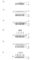
- (A) to (f) is a process diagram illustrating a method for producing a microstructure using the photopolymerizable resin composition according to the present embodiment.
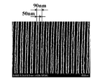
- 2 is an SEM photograph of a concavo-convex pattern (fine pattern) formed on the surface of a thin film made of the photopolymerizable resin composition of Example 1.
- FIG. 1A to FIG. 1F to be referred to are process diagrams for explaining a method for manufacturing a microstructure using the photopolymerizable resin composition according to the present embodiment.
- a microstructure 5 (see FIG. 1 (f)) in which a concavo-convex pattern corresponding to the concavo-convex pattern of a mold 2 (see FIG. 1 (b)) is formed on a substrate 3 (see FIG. 1 (a)). Is to be manufactured.
- the photopolymerizable resin composition 1 of the present invention described later is applied to the surface of the substrate 3.
- the substrate 3 include silicon (silicon), various metal materials, glass, quartz, ceramic, and resin.
- the substrate 3 may be a multilayer structure having a metal layer, a resin layer, an oxide film layer, or the like formed on the surface thereof.
- substrate 3 may be a thing by which the center hole was processed.
- the thin film 4 made of the photopolymerizable resin composition 1 is formed on the surface of the substrate 3 by spreading the photopolymerizable resin composition 1 on the substrate 3.
- a known coating method can be used.
- the spin coating method in which the thin film 4 is formed by spreading the photopolymerizable resin composition 1 by centrifugal force by rotating the substrate 3 is particularly preferable because the thin film 4 can be formed with a uniform thickness.
- symbol 2 is a metal mold
- the mold 2 has a concavo-convex pattern with a nanometer (nm) size on its surface, and the concavo-convex pattern in the present embodiment is a fine pattern with a size of several tens of nanometers.
- the method for forming the concavo-convex pattern include photolithography, focused ion beam lithography, electron beam drawing, and nanoprinting. These methods can be appropriately selected according to the processing accuracy of the uneven pattern.
- the material of the mold 2 is not particularly limited as long as it has a predetermined strength and can process a concavo-convex pattern (fine pattern) with a required accuracy.
- a silicon wafer various metal materials, Examples thereof include glass, quartz, ceramic, and resin material.
- a mold 2 made of quartz, Si, SiC, SiN, polycrystalline Si, Ni, Cr, Cu, a cured product of a photocurable resin material, or the like, and a mold 2 that is a combination of these two or more are preferable.
- a material of the mold 2 as will be described later, when the thin film 4 is irradiated with ultraviolet light through the mold 2 (see FIG. 1D), it is necessary to have transparency.
- quartz having high transparency is preferable.
- the mold 2 when a transparent substrate is used as the substrate 3 and the thin film 4 is irradiated with ultraviolet light from the substrate 3 side, the mold 2 is formed of an opaque material. Can do.
- the mold 2 made of an elastically deformable resin material has a foreign object (not shown) on the surface of the substrate 3 when the mold 2 is pressed against the thin film 4. ) Is also preferable because the non-contact area of the mold 2 generated around the foreign substance can be minimized by elastically deforming the mold 2 according to the shape of the foreign substance.
- the thin film 4 is irradiated with ultraviolet light (wavelength 365 nm) from the back surface of the mold 2 (surface opposite to the thin film 4). Is cured.
- the mold 2 is peeled from the thin film 4 to obtain the thin film 4 to which the uneven pattern of the mold 2 is transferred. Then, the substrate 3 is etched using the thin film 4 as a resist film.
- the substrate 3 is etched using the convex portions of the thin film 4 in FIG. 1 (b)), a fine structure 5 having a concavo-convex pattern corresponding to the concavo-convex pattern (fine pattern) on the substrate 3 can be obtained.
- the photopolymerizable resin composition 1 has a 6 to 15 functional acrylate as the component (A) and a weight average molecular weight (Mw) as the component (B) of 1000. ⁇ 10000 acrylate, acrylate having a benzene ring as component (C), reactive diluent as component (D), photopolymerization initiator as component (E), in a predetermined ratio described later It consists of
- 6-15 functional acrylates include acrylate monomers or oligomers having 6-15 acrylic groups, such as dipentaerythritol hexaacrylate. Further, 6-15 functional urethane acrylate, polyester acrylate, or the like may be used.
- the polyfunctional urethane acrylate a compound obtained by a urethanization reaction between an acrylate monomer having an acryloyl group and a hydroxyl group and a polyisocyanate can be used.
- polyfunctional urethane acrylate commercially available products can be used.
- UV-1700B manufactured by Nippon Synthetic Chemical Co., Ltd., urethane acrylate oligomer, 6 functional or more
- UA-53H manufactured by Shin-Nakamura Chemical Co., Ltd., urethane acrylate oligomer, 15 functional
- EBECRYL registered trademark
- UN-3320HA manufactured by Negami Kogyo Co., urethane acrylate, 6 functional
- a commercial item can be used for polyfunctional polyester acrylate, for example, EBECRYL1830 (the Daicel-Cytec company make, polyester acrylate oligomer, 6 functionals), EBECRYL450 (Daicel-Cytech company make, polyester acrylate oligomer, 6 functionals) etc. Is mentioned.
- the ratio of the component (A) in the photopolymerizable resin composition is 0.5 to 10% by mass.
- the photopolymerizable resin composition containing the component (A) within such a range has a transfer accuracy of the concavo-convex pattern (fine pattern). (Molding accuracy) will be excellent.
- the acrylate having a weight average molecular weight (Mw) of 1000 to 10,000 include poly (meth) acrylate, ethoxylated bisphenol A acrylate, aromatic urethane acrylate, aliphatic urethane acrylate, polyester acrylate, and the like.
- Examples of commercially available products include EBECRYL8405 (manufactured by Daicel-Cytec, urethane acrylate oligomer, tetrafunctional, weight average molecular weight (Mw) 2700), UV-7000B (manufactured by Nippon Synthetic Chemical Co., Ltd., urethane acrylate oligomer, bifunctional, weight average).
- Molecular weight (Mw) 5000 Molecular weight (Mw) 5000). These acrylates as component (B) can be used in combination of two or more. As the component (B), a component having a weight average molecular weight (Mw) of 1000 to 10,000 among the components (A) described above can also be used.
- the ratio of the component (B) in the photopolymerizable resin composition is 0.5 to 10% by mass.
- the photopolymerizable resin composition containing the component (B) in such a range exhibits excellent film formability when the thin film 4 (see FIG. 1B) is formed on the substrate 3.
- acrylate having a benzene ring an acrylate monomer having an acryloyl group and a benzene ring is used. Specific examples thereof include phenoxy glycol acrylate, phenoxy ethylene glycol acrylate, phenoxy polyethylene glycol acrylate, ethoxylated bisphenol A diacrylate, propoxylated bisphenol A diacrylate, and benzyl acrylate.
- the proportion of component (C) in the photopolymerizable resin composition is 0.5 to 10% by mass.
- the photopolymerizable resin composition containing the component (C) within such a range has excellent etching resistance when etching the substrate 3 using the cured thin film 4 as a resist film, as shown in FIG. Will be demonstrated.
- the reactive diluent mainly reduces the viscosity of the photopolymerizable resin composition by diluting the component (C) from the component (A).
- the reactive diluent is not particularly limited as long as it has a functional group capable of undergoing a crosslinking reaction with the component (A) to the component (C), but is preferably a monomer. Among these, a monomer having at least one (meth) acrylate group, vinyl group, epoxy group, and oxetanyl group at the terminal is desirable.
- reactive diluents examples include N-vinylpyrrolidone, acryloylmorpholine, N, N-dimethylacrylamide, N-methylolacrylamide, N, N-dimethylaminopropylacrylamide, vinyl (meth) acrylate, allyl (meth) acrylate.
- These reactive diluents can be used in combination of two or more.
- (meth) acrylate having a viscosity at 25 ° C. of 3 mPa ⁇ s or less is desirable.
- (meth) acrylates having a linear alkylene group having 1 to 6 carbon atoms are desirable, and substituents other than hydrogen atoms (for example, alkyl groups)
- (Meth) acrylates having an alkylene group that does not have a hydroxyl group or the like (however, except for an alkoxy group that is branched to form an ether) at the branching position are desirable.
- Such desirable reactive diluents include methyl (meth) acrylate, ethyl (meth) acrylate, butyl (meth) acrylate, hexyl (meth) acrylate, 2-methoxyethyl (meth) acrylate, 2-ethoxyethyl (meth) ) Acrylate, 3-methoxybutyl (meth) acrylate, allyl (meth) acrylate, soot and cyano (meth) acrylate.
- the proportion of component (D) in the photopolymerizable resin composition is 80 to 98% by mass.
- the photopolymerizable resin composition containing the component (D) in such a range has a thickness of several tens of nanometers when the thin film 4 is formed on the substrate 3 as shown in FIG. Can be formed.
- the reactive diluent having volatility described above can form a uniform thin film 4 without performing any baking process when the thin film 4 is formed on the substrate 3.
- the photoreaction initiator include radical polymerization initiators. Specific examples thereof include, for example, 1-hydroxy-cyclohexyl-phenyl ketone, 2-hydroxy-2-methyl-1-phenyl-propan-1-one, 1- [4- (2-hydroxyethoxy) -phenyl]- 2-hydroxy-2-methyl-1-propan-1-one, 2-hydroxy-1- ⁇ 4- [4- (2-hydroxy-2-methyl-propionyl) -benzyl] phenyl ⁇ -2-methyl-propane -1-one, 2-methyl-1- (4-methylthiophenyl) -2-morpholinpropan-1-one, 2-benzyl-2-dimethylamino-1- (4-morpholinophenyl) -butanone, , 2- (dimethylamino) -2-[(4-methylphenyl) methyl] -1- [4- (4-morpholinyl) phenyl] -1-butanone, 2- (dimethylamino) -2-[(4-
- the ratio of the component (E) in the photopolymerizable resin composition is 0.1 to 5% by mass. In such a range, the photopolymerizable resin composition containing the component (E), as shown in FIG. 1 (d), is promptly exposed when the thin film 4 (photopolymerizable resin composition) is irradiated with ultraviolet light. Can be cured.
- the conventional photopolymerizable resin composition for example, patent document) 1 and Patent Document 2
- a thinner and more uniform thin film can be formed, transfer accuracy of a finer and finer pattern can be improved, and the curing time of the formed thin film is shorter, and the throughput performance is higher than the conventional one. It is possible to provide a photopolymerizable resin composition for fine structure transfer that can produce an improved fine structure.
- Component (F) is a bifunctional acrylate having a viscosity at 25 ° C. of 12 mPa ⁇ s or less. Specific examples thereof include, for example, polyethylene glycol diacrylate, polypropylene glycol diacrylate, 1,4-butanediol diacrylate, 1,6-hexanediol diacrylate, 1,9-nonanediol diacrylate, neopentyl glycol diacrylate. Etc.
- the proportion of component (A) in the photopolymerizable resin composition is 0.1 to 5% by mass, the proportion of component (B) is 0.5 to 10% by mass, and the proportion of component (C) is 0.5%. 10% by mass, the proportion of component (D) is 80-98% by mass, the proportion of component (E) is 0.1-5% by mass, and the proportion of component (F) is 0.5- 10% by mass.
- the photopolymerizable resin composition containing the component (A) to the component (E) described above is more film forming and faster than the conventional photopolymerizable resin composition.
- the place which is excellent in curability and pattern moldability, and by containing a component (F) there exists an effect which further improves pattern moldability, without making film-forming property and quick-curability hardly deteriorated.
- the viscosity at 25 ° C. is 3 mPa ⁇ s.
- a photopolymerizable resin composition contains a reactive diluent composed of a monofunctional (meth) acrylate, so that when irradiated with ultraviolet light, it is more than a polyfunctional (meth) acrylate.
- the thin film can be cured in a short time.
- a photopolymerizable resin composition by including volatile (meth) acrylate, more specifically, (meth) acrylate having a linear alkylene group having 1 to 6 carbon atoms can be obtained. By including, a uniform thin film can be formed on the substrate without performing a baking process.
- the fine structure manufactured using the above photopolymerizable resin composition is applicable to information recording media such as magnetic recording media and optical recording media.
- This microstructure can be applied to large-scale integrated circuit components, optical components such as lenses, polarizing plates, wavelength filters, light-emitting elements, and optical integrated circuits, and biodevices such as immunoanalysis, DNA separation, and cell culture. It is.
- the microstructure in the embodiment is composed of a substrate etched with a resist film made by curing the thin film 4 made of the photopolymerizable resin composition according to the present embodiment, as shown in FIG.
- the thin film 4 to which the uneven pattern (fine pattern) shown is cured on the substrate 3 can be used as the fine structure.
- the photopolymerizable resin composition according to the embodiment may contain other components such as a surfactant and a polymerization inhibitor, if necessary.
- Example 1 the composition [mass%] of each component in the photopolymerizable resin composition is simply abbreviated as [%].
- Example 1 the components (A) to (E) are mixed so as to have the composition [%] shown in the following Table 1, and then the mixture is filtered through a polypropylene filter having a diameter of 100 nm. Thus, a desired photopolymerizable resin composition was obtained.
- component (A) hexafunctional acrylate (manufactured by Shin-Nakamura Chemical Co., Ltd., dipentaerythritol hexaacrylate) was used.
- component (B) acrylate having a weight average molecular weight (Mw) of 1000 to 10,000”, an acrylate having a weight average molecular weight (Mw) of 5000 (manufactured by Nippon Synthetic Chemical Co., Ltd., trade name UV-7000B, bifunctional to trifunctional urethane acrylate) )It was used.
- acrylate having a benzene ring as the component (C), an acrylate having a benzyl group (manufactured by Hitachi Chemical Co., Ltd., benzyl acrylate) was used.
- reactive diluent of component (D)
- a reactive diluent having a volatility butyl acrylate, manufactured by Tokyo Chemical Industry Co., Ltd.
- photopolymerization initiator of component (E)
- a radical polymerization initiator manufactured by Ciba Japan, IRGACURE (registered trademark) 369) was used.
- a microstructure 5 (see FIG. 1 (f)) was produced in the steps shown in FIGS. 1 (a) to (f).
- a silicon (Si) wafer having a thickness of 0.625 mm and a diameter of 65 mm was used.
- 500 ⁇ L of the photopolymerizable resin composition 1 was dropped using a micropipette.
- the photopolymerizable resin composition 1 dropped on the substrate 3 was spread by a spin coating method to form a thin film 4 shown in FIG.
- the spin coating method was performed under conditions of a rotation speed of 5000 rpm and a rotation time of 60 seconds. And the thickness of the thin film 4 was measured with the ellipsometer about 12 points in the surface of the formed thin film 4. As a result, it was confirmed that the thin film 4 had a uniform thickness in the range of 45 ⁇ 2 nm.
- the mold 2 was pressed against the thin film 4 to transfer the uneven pattern (fine pattern) of the mold 2 to the thin film 4.
- a circular quartz product having a thickness of 0.7 mm and a diameter of 150 mm was used.
- the concave / convex pattern (fine pattern) of the mold 2 is a pattern (line width 50 nm, pitch 90 nm, 40 nm).
- the mold 2 was pressed against the thin film 4 with a pressure of 0.2 MPa.
- the photopolymerizability is obtained by irradiating the thin film 4 with ultraviolet light (wavelength 365 nm) through a mold 2 using a predetermined ultraviolet lamp (not shown).
- the thin film 4 made of the resin composition 1 was cured.
- the thin film 4 can be cured with an irradiation amount (irradiation time) slightly smaller than usual when an ultraviolet ray irradiation amount of 100 mJ / cm 2 , that is, a predetermined output ultraviolet lamp is used.
- FIG.1 (e) the thin film 4 to which the uneven
- a concavo-convex pattern (fine pattern) composed of lines and spaces formed concentrically with a line width of 50 nm and a pitch of 90 nm was confirmed on the surface.
- FIG. 2 is an SEM photograph of a concavo-convex pattern (fine pattern) formed on the surface of a thin film made of the photopolymerizable resin composition of Example 1.
- the microstructure 3 was obtained by etching the substrate 3 using the thin film 4 to which the concavo-convex pattern (fine pattern) was transferred as a resist film. At this time, etching with oxygen plasma was performed until the surface of the substrate 3 was exposed, and then etching with fluorine-based gas plasma was performed in place of oxygen plasma to obtain the microstructure 5.
- the surface of the fine structure 5 was observed by SEM, as shown in FIG. 2, the surface was formed concentrically with a line width of 50 nm and a pitch of 90 nm. That is, it was confirmed that the thin film 4 formed by curing the photopolymerizable resin composition 1 (see FIG. 1A) exhibits sufficient etching resistance.
- Example 2 was the same as Example 1 except that instead of 6-functional acrylate, 15-functional acrylate (manufactured by Shin-Nakamura Chemical Co., Ltd., urethane acrylate oligomer, trade name UA-53H) was used as component (A).
- a photopolymerizable resin composition was prepared, and a microstructure 5 (see FIG. 1 (f)) was obtained using this photopolymerizable resin composition.
- the thin film 4 see FIG. 1E
- the film-forming property, curability, and transfer accuracy of the photopolymerizable resin composition obtained in this example were evaluated in the same manner as in Example 1. The results are shown in Table 1.
- Example 3 In Example 3, as an ingredient (B), an acrylate having a weight average molecular weight (Mw) of 5000 instead of an acrylate having a weight average molecular weight (Mw) of 2700 (manufactured by Nippon Synthetic Chemical Co., Ltd., urethane acrylate oligomer, trade name UV-7000B) A photopolymerizable resin composition was prepared in the same manner as in Example 1 except that was used, and a microstructure 5 (see FIG. 1 (f)) was obtained using this photopolymerizable resin composition. At this time, it was confirmed that the thin film 4 (see FIG. 1E) formed by curing the photopolymerizable resin composition exhibits sufficient etching resistance. The film-forming property, curability, and transfer accuracy of the photopolymerizable resin composition obtained in this example were evaluated in the same manner as in Example 1. The results are shown in Table 1.
- Example 4 In Example 4, volatile 2-methoxyethyl acrylate (manufactured by Tokyo Chemical Industry Co., Ltd.) was used as the component (D) instead of butyl acrylate, and the components (A) to (E) were changed from Table 1
- a photopolymerizable resin composition was prepared in the same manner as in Example 1 except that the composition [%] shown in FIG. 1 was used, and the microstructure 5 (see FIG. 1 (f)) was prepared using this photopolymerizable resin composition. )
- the thin film 4 see FIG. 1E) formed by curing the photopolymerizable resin composition exhibits sufficient etching resistance.
- the film-forming property, curability, and transfer accuracy of the photopolymerizable resin composition obtained in this example were evaluated in the same manner as in Example 1. The results are shown in Table 1.
- Example 5 In Example 5, the components (A) to (F) were mixed so as to have the composition [%] shown in Table 1, and the mixture was then filtered through a polypropylene filter having an opening of 100 nm in diameter. The intended photopolymerizable resin composition was obtained.
- component (A) hexafunctional acrylate (manufactured by Shin-Nakamura Chemical Co., Ltd., dipentaerythritol ethoxylate hexaacrylate) was used.
- component (B) an acrylate having a weight average molecular weight (Mw) of 5000 (manufactured by Nippon Synthetic Chemical Co., Ltd., trade name UV-3000B, bifunctional urethane acrylate) is used. used.
- acrylate having a benzene ring As the “acrylate having a benzene ring” as the component (C), an acrylate having a benzyl group (manufactured by Hitachi Chemical Co., Ltd., benzyl acrylate) was used.
- reactive diluent As the “reactive diluent” of component (D), a reactive diluent having a volatility (Butyl acrylate, manufactured by Tokyo Chemical Industry Co., Ltd.) was used.
- photopolymerization initiator As the “photopolymerization initiator” of component (E), a radical polymerization initiator (manufactured by Ciba Japan, IRGACURE (registered trademark) 369) was used.
- component (F) “bifunctional acrylate having a viscosity at 25 ° C.
- Comparative Example 1 a photopolymerizable resin composition was prepared in the same manner as in Example 1 except that the composition of Component (C) and Component (D) was changed as shown in Table 1. And when it tried to form the thin film 4 shown in FIG.1 (b) by the spin coat method using this photopolymerizable resin composition similarly to Example 1, the thickness of the thin film 4 was 500 nm or more. became. Therefore, as shown in Table 1, the evaluation result of the film formability in the photopolymerizable resin composition of Comparative Example 1 was “bad”. In addition, in the photopolymerizable resin composition of Comparative Example 1, since the film formability was evaluated as “poor”, the curability and the transfer accuracy were not evaluated.
- Comparative Example 2 In Comparative Example 2, a bifunctional acrylate (manufactured by Tokyo Chemical Industry Co., Ltd., 1,4-butanediol diacrylate) shown as a component (A) ′ in Table 1 was used instead of the hexafunctional acrylate as the component (A).
- a photopolymerizable resin composition was prepared in the same manner as in Example 1 except that it was used, and a thin film 4 having a concavo-convex pattern (fine pattern) transferred as shown in FIG. At this time, the film formability and curability of the photopolymerizable resin composition of Comparative Example 2 were good, and the evaluation result was “good” as shown in Table 1.
- Comparative Example 3 In Comparative Example 3, a bifunctional acrylate (manufactured by Tokyo Chemical Industry Co., Ltd., 1,4-butanediol diacrylate) shown as a component (A) ′ in Table 1 was used instead of the hexafunctional acrylate as the component (A).
- a photopolymerizable resin composition was prepared in the same manner as in Example 1 except that 10% was used and the component (B) to component (E) were changed to the composition [%] shown in Table 1. And when it tried to form the thin film 4 shown in FIG.1 (b) by the spin coat method using this photopolymerizable resin composition like Example 1, the thickness of the thin film 4 was 200 nm or more. became.
- Comparative Example 4 In Comparative Example 4, as the component (B), an acrylate having a weight average molecular weight (Mw) of 500 shown as a component (B) ′ in Table 1 instead of an acrylate having a weight average molecular weight (Mw) of 2700 (Daicel Cytec Co., Ltd.) A photopolymerizable resin composition was prepared in the same manner as in Example 1 except that the product name EBECRYL600, bifunctional bisphenol A epoxy acrylate) was used.
- EBECRYL600 bifunctional bisphenol A epoxy acrylate
- the thin film 4 spread on the substrate 3 was: The film contracted due to surface tension over time, and the film could not be maintained. Therefore, as shown in Table 1, the evaluation result of the film formability in the photopolymerizable resin composition of Comparative Example 1 was “bad”. In addition, in the photopolymerizable resin composition of Comparative Example 1, since the film formability was evaluated as “poor”, the curability and the transfer accuracy were not evaluated.
- Comparative Example 5 In Comparative Example 5, instead of acrylate having a phenoxy group as component (C), benzyl methacrylate (made by Hitachi Chemical Co., Ltd.), which is not acrylate, shown as component (C) ′ in Table 1, was used.
- a photopolymerizable resin composition was prepared in the same manner as in Example 1, and a thin film 4 was obtained on a substrate 3 by spin coating as shown in FIG. The thickness of the thin film 4 was 46 ⁇ 3 nm and was confirmed to be a uniform film. Therefore, as shown in Table 1, the film forming property evaluation result in the photopolymerizable resin composition of Comparative Example 5 was “good”. However, as shown in FIG.
- the photopolymerizable resin composition containing the component (A) to the component (E) in a predetermined ratio can form a thin and uniform thin film of 50 nm or less, and is less than 100 nm size.
- a photopolymerizable resin that is capable of producing a microstructure 5 (see FIG. 1 (f)) that has excellent transfer accuracy of a fine pattern and that has a short curing time of the formed thin film and has improved throughput. It was confirmed to be a composition.
Landscapes
- Chemical & Material Sciences (AREA)
- Health & Medical Sciences (AREA)
- Chemical Kinetics & Catalysis (AREA)
- Medicinal Chemistry (AREA)
- Polymers & Plastics (AREA)
- Organic Chemistry (AREA)
- Exposure Of Semiconductors, Excluding Electron Or Ion Beam Exposure (AREA)
- Macromonomer-Based Addition Polymer (AREA)
- Manufacturing Of Magnetic Record Carriers (AREA)
- Addition Polymer Or Copolymer, Post-Treatments, Or Chemical Modifications (AREA)
Applications Claiming Priority (2)
| Application Number | Priority Date | Filing Date | Title |
|---|---|---|---|
| JP2010169956A JP2012031240A (ja) | 2010-07-29 | 2010-07-29 | 微細構造転写用の光重合性樹脂組成物 |
| JP2010-169956 | 2010-07-29 |
Publications (1)
| Publication Number | Publication Date |
|---|---|
| WO2012014961A1 true WO2012014961A1 (ja) | 2012-02-02 |
Family
ID=45527356
Family Applications (1)
| Application Number | Title | Priority Date | Filing Date |
|---|---|---|---|
| PCT/JP2011/067217 Ceased WO2012014961A1 (ja) | 2010-07-29 | 2011-07-28 | 微細構造転写用の光重合性樹脂組成物 |
Country Status (3)
| Country | Link |
|---|---|
| US (1) | US20120029110A1 (enExample) |
| JP (1) | JP2012031240A (enExample) |
| WO (1) | WO2012014961A1 (enExample) |
Cited By (2)
| Publication number | Priority date | Publication date | Assignee | Title |
|---|---|---|---|---|
| WO2013176020A1 (ja) * | 2012-05-25 | 2013-11-28 | 綜研化学株式会社 | インプリント用光硬化性樹脂組成物、その製造方法および構造体 |
| WO2014065149A1 (ja) * | 2012-10-22 | 2014-05-01 | 綜研化学株式会社 | インプリント用光硬化性樹脂組成物、インプリント用モールドの製造方法およびインプリント用モールド |
Families Citing this family (8)
| Publication number | Priority date | Publication date | Assignee | Title |
|---|---|---|---|---|
| JP6037627B2 (ja) * | 2011-03-30 | 2016-12-07 | 協立化学産業株式会社 | インプリント成型用光硬化性樹脂組成物、インプリント成型硬化体及びこれらの製造方法 |
| JP6460672B2 (ja) | 2013-09-18 | 2019-01-30 | キヤノン株式会社 | 膜の製造方法、光学部品の製造方法、回路基板の製造方法及び電子部品の製造方法 |
| US10113066B2 (en) | 2013-11-05 | 2018-10-30 | Taiyo Ink Mfg. Co., Ltd. | Curable composition, cured coating film using same, and printed wiring board |
| JP6339346B2 (ja) * | 2013-11-05 | 2018-06-06 | 太陽インキ製造株式会社 | プリント配線板用硬化型組成物、これを用いた硬化塗膜及びプリント配線板 |
| KR102450569B1 (ko) * | 2014-02-04 | 2022-10-04 | 데쿠세리아루즈 가부시키가이샤 | 이방성 도전 필름 및 그 제조 방법 |
| JP6797529B2 (ja) * | 2015-01-21 | 2020-12-09 | 東洋合成工業株式会社 | 光学部材の製造方法及びそれに用いられる組成物 |
| WO2019237228A1 (zh) * | 2018-06-11 | 2019-12-19 | 厦门三安光电有限公司 | 发光组件 |
| JP7490476B2 (ja) * | 2019-08-20 | 2024-05-27 | キヤノン株式会社 | インプリント方法、インプリント装置、および物品の製造方法 |
Citations (6)
| Publication number | Priority date | Publication date | Assignee | Title |
|---|---|---|---|---|
| JP2003160623A (ja) * | 2001-11-26 | 2003-06-03 | Toagosei Co Ltd | 光学部材用活性エネルギー線硬化型組成物 |
| JP2004284178A (ja) * | 2003-03-20 | 2004-10-14 | Dainippon Printing Co Ltd | 賦型方法、賦型フィルム、及び射出成形品 |
| JP2004352781A (ja) * | 2003-05-27 | 2004-12-16 | San Nopco Ltd | 放射線硬化性組成物 |
| JP2006063144A (ja) * | 2004-08-25 | 2006-03-09 | Jsr Corp | 液状硬化性樹脂組成物 |
| WO2007040159A1 (ja) * | 2005-10-04 | 2007-04-12 | The Inctec Inc. | 特定の表面形状と物性を有する構造体及びその構造体形成用の(メタ)アクリル系重合性組成物 |
| WO2011115162A1 (ja) * | 2010-03-17 | 2011-09-22 | 三菱レイヨン株式会社 | 活性エネルギー線硬化性樹脂組成物および微細凹凸構造を表面に有する物品 |
Family Cites Families (5)
| Publication number | Priority date | Publication date | Assignee | Title |
|---|---|---|---|---|
| US4668558A (en) * | 1978-07-20 | 1987-05-26 | Minnesota Mining And Manufacturing Company | Shaped plastic articles having replicated microstructure surfaces |
| US5626800A (en) * | 1995-02-03 | 1997-05-06 | Minnesota Mining And Manufacturing Company | Prevention of groove tip deformation in brightness enhancement film |
| KR100568581B1 (ko) * | 2003-04-14 | 2006-04-07 | 주식회사 미뉴타텍 | 미세패턴 형성 몰드용 조성물 및 이로부터 제작된 몰드 |
| JP4770354B2 (ja) * | 2005-09-20 | 2011-09-14 | 日立化成工業株式会社 | 光硬化性樹脂組成物及びこれを用いたパターン形成方法 |
| JP5243887B2 (ja) * | 2008-02-12 | 2013-07-24 | 富士フイルム株式会社 | ナノインプリント用硬化性組成物およびパターン形成方法 |
-
2010
- 2010-07-29 JP JP2010169956A patent/JP2012031240A/ja not_active Abandoned
-
2011
- 2011-07-28 WO PCT/JP2011/067217 patent/WO2012014961A1/ja not_active Ceased
- 2011-07-29 US US13/193,658 patent/US20120029110A1/en not_active Abandoned
Patent Citations (6)
| Publication number | Priority date | Publication date | Assignee | Title |
|---|---|---|---|---|
| JP2003160623A (ja) * | 2001-11-26 | 2003-06-03 | Toagosei Co Ltd | 光学部材用活性エネルギー線硬化型組成物 |
| JP2004284178A (ja) * | 2003-03-20 | 2004-10-14 | Dainippon Printing Co Ltd | 賦型方法、賦型フィルム、及び射出成形品 |
| JP2004352781A (ja) * | 2003-05-27 | 2004-12-16 | San Nopco Ltd | 放射線硬化性組成物 |
| JP2006063144A (ja) * | 2004-08-25 | 2006-03-09 | Jsr Corp | 液状硬化性樹脂組成物 |
| WO2007040159A1 (ja) * | 2005-10-04 | 2007-04-12 | The Inctec Inc. | 特定の表面形状と物性を有する構造体及びその構造体形成用の(メタ)アクリル系重合性組成物 |
| WO2011115162A1 (ja) * | 2010-03-17 | 2011-09-22 | 三菱レイヨン株式会社 | 活性エネルギー線硬化性樹脂組成物および微細凹凸構造を表面に有する物品 |
Cited By (4)
| Publication number | Priority date | Publication date | Assignee | Title |
|---|---|---|---|---|
| WO2013176020A1 (ja) * | 2012-05-25 | 2013-11-28 | 綜研化学株式会社 | インプリント用光硬化性樹脂組成物、その製造方法および構造体 |
| WO2014065149A1 (ja) * | 2012-10-22 | 2014-05-01 | 綜研化学株式会社 | インプリント用光硬化性樹脂組成物、インプリント用モールドの製造方法およびインプリント用モールド |
| CN104737272A (zh) * | 2012-10-22 | 2015-06-24 | 综研化学株式会社 | 压印用光固化性树脂组合物、压印用模具的制造方法以及压印用模具 |
| JPWO2014065149A1 (ja) * | 2012-10-22 | 2016-09-08 | 綜研化学株式会社 | インプリント用光硬化性樹脂組成物、インプリント用モールドの製造方法およびインプリント用モールド |
Also Published As
| Publication number | Publication date |
|---|---|
| US20120029110A1 (en) | 2012-02-02 |
| JP2012031240A (ja) | 2012-02-16 |
Similar Documents
| Publication | Publication Date | Title |
|---|---|---|
| WO2012014961A1 (ja) | 微細構造転写用の光重合性樹脂組成物 | |
| US8980404B2 (en) | Composition for imprints, pattern and patterning method | |
| US9868846B2 (en) | Curable composition for imprints, patterning method and pattern | |
| JP5710553B2 (ja) | インプリント用硬化性組成物、パターン形成方法およびパターン | |
| JP5033867B2 (ja) | 微細構造体、微細構造体の製造方法、及び微細構造体製造用の重合性樹脂組成物 | |
| JP5481861B2 (ja) | 光硬化性樹脂組成物、これを用いたパターン形成方法及び微細構造体 | |
| TW200923583A (en) | Curable composition for photonano-imprinting and member for liquid crystal display device by using it | |
| TW200846824A (en) | Curing composition for photonano-imprinting lithography and pattern forming method by using the same | |
| JP2007186570A (ja) | 光硬化性樹脂組成物及びパターン形成法 | |
| TW201439181A (zh) | 組成物、硬化物、積層體、下層膜之製造方法、圖案形成方法、圖案及半導體抗蝕層之製造方法 | |
| JP2009206197A (ja) | ナノインプリント用硬化性組成物、硬化物およびその製造方法 | |
| JP5753749B2 (ja) | インプリント用硬化性組成物の製造方法 | |
| TW201213353A (en) | Composition for photocurable imprint, and method for formation of pattern using the composition | |
| WO2015046134A1 (ja) | 光インプリント用硬化性組成物及びパターン形成方法 | |
| WO2014050855A1 (ja) | 光インプリント用硬化性組成物、パターン形成方法、微細パターンおよび半導体デバイスの製造方法 | |
| CN101959932A (zh) | 纳米压印用固化性组合物、使用它的固化物及其制造方法、以及液晶显示装置用构件 | |
| CN106886127B (zh) | 光压印树脂组合物、光压印树脂膜以及图案化制程 | |
| JP2014157955A (ja) | 微細構造形成方法及び微細構造形成体 | |
| JP2008084984A (ja) | 光ナノインプリントリソグラフィ用光硬化性組成物およびそれを用いたパターン形成方法 | |
| JP5448589B2 (ja) | パターン形成方法 | |
| JP5349854B2 (ja) | 微細構造体およびその製造方法 | |
| JP2011082347A (ja) | インプリント用硬化性組成物、硬化物の製造方法および硬化物 | |
| JP2009073958A (ja) | ナノインプリントリソグラフィ用硬化性組成物、それを用いた硬化物作成方法、および、硬化物 | |
| WO2017150261A1 (ja) | パターン積層体の製造方法、反転パターンの製造方法およびパターン積層体 | |
| KR20230003292A (ko) | 모놀리식 고굴절률 광자 디바이스들 |
Legal Events
| Date | Code | Title | Description |
|---|---|---|---|
| 121 | Ep: the epo has been informed by wipo that ep was designated in this application |
Ref document number: 11812550 Country of ref document: EP Kind code of ref document: A1 |
|
| NENP | Non-entry into the national phase |
Ref country code: DE |
|
| 122 | Ep: pct application non-entry in european phase |
Ref document number: 11812550 Country of ref document: EP Kind code of ref document: A1 |