WO2012014961A1 - Photopolymerizable resin composition for use in transferring microstructure - Google Patents
Photopolymerizable resin composition for use in transferring microstructure Download PDFInfo
- Publication number
- WO2012014961A1 WO2012014961A1 PCT/JP2011/067217 JP2011067217W WO2012014961A1 WO 2012014961 A1 WO2012014961 A1 WO 2012014961A1 JP 2011067217 W JP2011067217 W JP 2011067217W WO 2012014961 A1 WO2012014961 A1 WO 2012014961A1
- Authority
- WO
- WIPO (PCT)
- Prior art keywords
- resin composition
- component
- acrylate
- photopolymerizable resin
- thin film
- Prior art date
Links
- 239000011342 resin composition Substances 0.000 title claims abstract description 108
- NIXOWILDQLNWCW-UHFFFAOYSA-M Acrylate Chemical compound [O-]C(=O)C=C NIXOWILDQLNWCW-UHFFFAOYSA-M 0.000 claims abstract description 80
- 239000003085 diluting agent Substances 0.000 claims abstract description 26
- 239000003999 initiator Substances 0.000 claims abstract description 9
- 125000001997 phenyl group Chemical group [H]C1=C([H])C([H])=C(*)C([H])=C1[H] 0.000 claims abstract description 8
- 238000012546 transfer Methods 0.000 claims description 34
- 230000001588 bifunctional effect Effects 0.000 claims description 10
- 239000010409 thin film Substances 0.000 description 84
- 239000000758 substrate Substances 0.000 description 43
- 238000000034 method Methods 0.000 description 31
- 230000000052 comparative effect Effects 0.000 description 20
- 239000010408 film Substances 0.000 description 20
- UHESRSKEBRADOO-UHFFFAOYSA-N ethyl carbamate;prop-2-enoic acid Chemical compound OC(=O)C=C.CCOC(N)=O UHESRSKEBRADOO-UHFFFAOYSA-N 0.000 description 15
- 238000005530 etching Methods 0.000 description 13
- 238000001723 curing Methods 0.000 description 11
- 239000011347 resin Substances 0.000 description 10
- 229920005989 resin Polymers 0.000 description 10
- 239000000203 mixture Substances 0.000 description 9
- 238000010894 electron beam technology Methods 0.000 description 8
- 238000011156 evaluation Methods 0.000 description 8
- 238000004519 manufacturing process Methods 0.000 description 8
- 239000000126 substance Substances 0.000 description 8
- UHOVQNZJYSORNB-UHFFFAOYSA-N Benzene Chemical group C1=CC=CC=C1 UHOVQNZJYSORNB-UHFFFAOYSA-N 0.000 description 6
- -1 ethoxylated bisphenol A acrylate Chemical class 0.000 description 6
- 239000000463 material Substances 0.000 description 6
- 239000004065 semiconductor Substances 0.000 description 6
- 150000001252 acrylic acid derivatives Chemical class 0.000 description 5
- 239000000178 monomer Substances 0.000 description 5
- 229920000728 polyester Polymers 0.000 description 5
- 239000010453 quartz Substances 0.000 description 5
- 230000007261 regionalization Effects 0.000 description 5
- VYPSYNLAJGMNEJ-UHFFFAOYSA-N silicon dioxide Inorganic materials O=[Si]=O VYPSYNLAJGMNEJ-UHFFFAOYSA-N 0.000 description 5
- 238000004528 spin coating Methods 0.000 description 5
- JHWGFJBTMHEZME-UHFFFAOYSA-N 4-prop-2-enoyloxybutyl prop-2-enoate Chemical compound C=CC(=O)OCCCCOC(=O)C=C JHWGFJBTMHEZME-UHFFFAOYSA-N 0.000 description 4
- XUIMIQQOPSSXEZ-UHFFFAOYSA-N Silicon Chemical compound [Si] XUIMIQQOPSSXEZ-UHFFFAOYSA-N 0.000 description 4
- 239000002184 metal Substances 0.000 description 4
- 229910052751 metal Inorganic materials 0.000 description 4
- 229910052710 silicon Inorganic materials 0.000 description 4
- 239000010703 silicon Substances 0.000 description 4
- 125000002947 alkylene group Chemical group 0.000 description 3
- GCTPMLUUWLLESL-UHFFFAOYSA-N benzyl prop-2-enoate Chemical compound C=CC(=O)OCC1=CC=CC=C1 GCTPMLUUWLLESL-UHFFFAOYSA-N 0.000 description 3
- CQEYYJKEWSMYFG-UHFFFAOYSA-N butyl acrylate Chemical compound CCCCOC(=O)C=C CQEYYJKEWSMYFG-UHFFFAOYSA-N 0.000 description 3
- 238000005516 engineering process Methods 0.000 description 3
- 239000004615 ingredient Substances 0.000 description 3
- 230000003287 optical effect Effects 0.000 description 3
- 125000000951 phenoxy group Chemical group [H]C1=C([H])C([H])=C(O*)C([H])=C1[H] 0.000 description 3
- 238000000206 photolithography Methods 0.000 description 3
- 239000007870 radical polymerization initiator Substances 0.000 description 3
- 238000003892 spreading Methods 0.000 description 3
- 125000003903 2-propenyl group Chemical group [H]C([*])([H])C([H])=C([H])[H] 0.000 description 2
- RTZKZFJDLAIYFH-UHFFFAOYSA-N Diethyl ether Chemical compound CCOCC RTZKZFJDLAIYFH-UHFFFAOYSA-N 0.000 description 2
- LYCAIKOWRPUZTN-UHFFFAOYSA-N Ethylene glycol Chemical compound OCCO LYCAIKOWRPUZTN-UHFFFAOYSA-N 0.000 description 2
- 239000002202 Polyethylene glycol Substances 0.000 description 2
- 239000004743 Polypropylene Substances 0.000 description 2
- MPIAGWXWVAHQBB-UHFFFAOYSA-N [3-prop-2-enoyloxy-2-[[3-prop-2-enoyloxy-2,2-bis(prop-2-enoyloxymethyl)propoxy]methyl]-2-(prop-2-enoyloxymethyl)propyl] prop-2-enoate Chemical compound C=CC(=O)OCC(COC(=O)C=C)(COC(=O)C=C)COCC(COC(=O)C=C)(COC(=O)C=C)COC(=O)C=C MPIAGWXWVAHQBB-UHFFFAOYSA-N 0.000 description 2
- FHLPGTXWCFQMIU-UHFFFAOYSA-N [4-[2-(4-prop-2-enoyloxyphenyl)propan-2-yl]phenyl] prop-2-enoate Chemical class C=1C=C(OC(=O)C=C)C=CC=1C(C)(C)C1=CC=C(OC(=O)C=C)C=C1 FHLPGTXWCFQMIU-UHFFFAOYSA-N 0.000 description 2
- NIXOWILDQLNWCW-UHFFFAOYSA-N acrylic acid group Chemical group C(C=C)(=O)O NIXOWILDQLNWCW-UHFFFAOYSA-N 0.000 description 2
- 125000003647 acryloyl group Chemical group O=C([*])C([H])=C([H])[H] 0.000 description 2
- QVGXLLKOCUKJST-UHFFFAOYSA-N atomic oxygen Chemical compound [O] QVGXLLKOCUKJST-UHFFFAOYSA-N 0.000 description 2
- 125000001797 benzyl group Chemical group [H]C1=C([H])C([H])=C(C([H])=C1[H])C([H])([H])* 0.000 description 2
- 230000015572 biosynthetic process Effects 0.000 description 2
- IISBACLAFKSPIT-UHFFFAOYSA-N bisphenol A Chemical compound C=1C=C(O)C=CC=1C(C)(C)C1=CC=C(O)C=C1 IISBACLAFKSPIT-UHFFFAOYSA-N 0.000 description 2
- 125000004432 carbon atom Chemical group C* 0.000 description 2
- 239000000919 ceramic Substances 0.000 description 2
- 238000006243 chemical reaction Methods 0.000 description 2
- 238000010586 diagram Methods 0.000 description 2
- GYZLOYUZLJXAJU-UHFFFAOYSA-N diglycidyl ether Chemical compound C1OC1COCC1CO1 GYZLOYUZLJXAJU-UHFFFAOYSA-N 0.000 description 2
- 239000011521 glass Substances 0.000 description 2
- 125000002887 hydroxy group Chemical group [H]O* 0.000 description 2
- 239000007769 metal material Substances 0.000 description 2
- 125000002496 methyl group Chemical group [H]C([H])([H])* 0.000 description 2
- 238000000465 moulding Methods 0.000 description 2
- 239000001301 oxygen Substances 0.000 description 2
- 229910052760 oxygen Inorganic materials 0.000 description 2
- 229920001223 polyethylene glycol Polymers 0.000 description 2
- 229920001155 polypropylene Polymers 0.000 description 2
- 238000012545 processing Methods 0.000 description 2
- 125000000391 vinyl group Chemical group [H]C([*])=C([H])[H] 0.000 description 2
- 239000012956 1-hydroxycyclohexylphenyl-ketone Substances 0.000 description 1
- XLPJNCYCZORXHG-UHFFFAOYSA-N 1-morpholin-4-ylprop-2-en-1-one Chemical compound C=CC(=O)N1CCOCC1 XLPJNCYCZORXHG-UHFFFAOYSA-N 0.000 description 1
- LYDOQHFHYWDZBS-UHFFFAOYSA-N 1-phenoxyethane-1,2-diol;prop-2-enoic acid Chemical compound OC(=O)C=C.OCC(O)OC1=CC=CC=C1 LYDOQHFHYWDZBS-UHFFFAOYSA-N 0.000 description 1
- STMDPCBYJCIZOD-UHFFFAOYSA-N 2-(2,4-dinitroanilino)-4-methylpentanoic acid Chemical compound CC(C)CC(C(O)=O)NC1=CC=C([N+]([O-])=O)C=C1[N+]([O-])=O STMDPCBYJCIZOD-UHFFFAOYSA-N 0.000 description 1
- BBBUAWSVILPJLL-UHFFFAOYSA-N 2-(2-ethylhexoxymethyl)oxirane Chemical compound CCCCC(CC)COCC1CO1 BBBUAWSVILPJLL-UHFFFAOYSA-N 0.000 description 1
- LJWZDTGRJUXOCE-UHFFFAOYSA-N 2-(2-ethylhexyl)oxetane Chemical compound CCCCC(CC)CC1CCO1 LJWZDTGRJUXOCE-UHFFFAOYSA-N 0.000 description 1
- PUBNJSZGANKUGX-UHFFFAOYSA-N 2-(dimethylamino)-2-[(4-methylphenyl)methyl]-1-(4-morpholin-4-ylphenyl)butan-1-one Chemical compound C=1C=C(N2CCOCC2)C=CC=1C(=O)C(CC)(N(C)C)CC1=CC=C(C)C=C1 PUBNJSZGANKUGX-UHFFFAOYSA-N 0.000 description 1
- GJKGAPPUXSSCFI-UHFFFAOYSA-N 2-Hydroxy-4'-(2-hydroxyethoxy)-2-methylpropiophenone Chemical compound CC(C)(O)C(=O)C1=CC=C(OCCO)C=C1 GJKGAPPUXSSCFI-UHFFFAOYSA-N 0.000 description 1
- TXBCBTDQIULDIA-UHFFFAOYSA-N 2-[[3-hydroxy-2,2-bis(hydroxymethyl)propoxy]methyl]-2-(hydroxymethyl)propane-1,3-diol Chemical compound OCC(CO)(CO)COCC(CO)(CO)CO TXBCBTDQIULDIA-UHFFFAOYSA-N 0.000 description 1
- PCKZAVNWRLEHIP-UHFFFAOYSA-N 2-hydroxy-1-[4-[[4-(2-hydroxy-2-methylpropanoyl)phenyl]methyl]phenyl]-2-methylpropan-1-one Chemical compound C1=CC(C(=O)C(C)(O)C)=CC=C1CC1=CC=C(C(=O)C(C)(C)O)C=C1 PCKZAVNWRLEHIP-UHFFFAOYSA-N 0.000 description 1
- XMLYCEVDHLAQEL-UHFFFAOYSA-N 2-hydroxy-2-methyl-1-phenylpropan-1-one Chemical compound CC(C)(O)C(=O)C1=CC=CC=C1 XMLYCEVDHLAQEL-UHFFFAOYSA-N 0.000 description 1
- 125000004200 2-methoxyethyl group Chemical group [H]C([H])([H])OC([H])([H])C([H])([H])* 0.000 description 1
- HFCUBKYHMMPGBY-UHFFFAOYSA-N 2-methoxyethyl prop-2-enoate Chemical compound COCCOC(=O)C=C HFCUBKYHMMPGBY-UHFFFAOYSA-N 0.000 description 1
- FIHBHSQYSYVZQE-UHFFFAOYSA-N 6-prop-2-enoyloxyhexyl prop-2-enoate Chemical compound C=CC(=O)OCCCCCCOC(=O)C=C FIHBHSQYSYVZQE-UHFFFAOYSA-N 0.000 description 1
- PGDIJTMOHORACQ-UHFFFAOYSA-N 9-prop-2-enoyloxynonyl prop-2-enoate Chemical compound C=CC(=O)OCCCCCCCCCOC(=O)C=C PGDIJTMOHORACQ-UHFFFAOYSA-N 0.000 description 1
- YCKRFDGAMUMZLT-UHFFFAOYSA-N Fluorine atom Chemical compound [F] YCKRFDGAMUMZLT-UHFFFAOYSA-N 0.000 description 1
- CNCOEDDPFOAUMB-UHFFFAOYSA-N N-Methylolacrylamide Chemical compound OCNC(=O)C=C CNCOEDDPFOAUMB-UHFFFAOYSA-N 0.000 description 1
- WHNWPMSKXPGLAX-UHFFFAOYSA-N N-Vinyl-2-pyrrolidone Chemical compound C=CN1CCCC1=O WHNWPMSKXPGLAX-UHFFFAOYSA-N 0.000 description 1
- FQYUMYWMJTYZTK-UHFFFAOYSA-N Phenyl glycidyl ether Chemical compound C1OC1COC1=CC=CC=C1 FQYUMYWMJTYZTK-UHFFFAOYSA-N 0.000 description 1
- 208000034189 Sclerosis Diseases 0.000 description 1
- 229910004541 SiN Inorganic materials 0.000 description 1
- VZTQQYMRXDUHDO-UHFFFAOYSA-N [2-hydroxy-3-[4-[2-[4-(2-hydroxy-3-prop-2-enoyloxypropoxy)phenyl]propan-2-yl]phenoxy]propyl] prop-2-enoate Chemical compound C=1C=C(OCC(O)COC(=O)C=C)C=CC=1C(C)(C)C1=CC=C(OCC(O)COC(=O)C=C)C=C1 VZTQQYMRXDUHDO-UHFFFAOYSA-N 0.000 description 1
- GUCYFKSBFREPBC-UHFFFAOYSA-N [phenyl-(2,4,6-trimethylbenzoyl)phosphoryl]-(2,4,6-trimethylphenyl)methanone Chemical compound CC1=CC(C)=CC(C)=C1C(=O)P(=O)(C=1C=CC=CC=1)C(=O)C1=C(C)C=C(C)C=C1C GUCYFKSBFREPBC-UHFFFAOYSA-N 0.000 description 1
- 125000001931 aliphatic group Chemical group 0.000 description 1
- 125000003545 alkoxy group Chemical group 0.000 description 1
- 125000000217 alkyl group Chemical group 0.000 description 1
- 238000013459 approach Methods 0.000 description 1
- 125000003118 aryl group Chemical group 0.000 description 1
- AOJOEFVRHOZDFN-UHFFFAOYSA-N benzyl 2-methylprop-2-enoate Chemical compound CC(=C)C(=O)OCC1=CC=CC=C1 AOJOEFVRHOZDFN-UHFFFAOYSA-N 0.000 description 1
- MQDJYUACMFCOFT-UHFFFAOYSA-N bis[2-(1-hydroxycyclohexyl)phenyl]methanone Chemical compound C=1C=CC=C(C(=O)C=2C(=CC=CC=2)C2(O)CCCCC2)C=1C1(O)CCCCC1 MQDJYUACMFCOFT-UHFFFAOYSA-N 0.000 description 1
- 125000000484 butyl group Chemical group [H]C([*])([H])C([H])([H])C([H])([H])C([H])([H])[H] 0.000 description 1
- 238000004113 cell culture Methods 0.000 description 1
- 229910052804 chromium Inorganic materials 0.000 description 1
- 238000000576 coating method Methods 0.000 description 1
- 150000001875 compounds Chemical class 0.000 description 1
- 229910052802 copper Inorganic materials 0.000 description 1
- 238000004132 cross linking Methods 0.000 description 1
- 125000004093 cyano group Chemical group *C#N 0.000 description 1
- 238000011161 development Methods 0.000 description 1
- 230000018109 developmental process Effects 0.000 description 1
- 125000004386 diacrylate group Chemical group 0.000 description 1
- 238000007865 diluting Methods 0.000 description 1
- 125000002147 dimethylamino group Chemical group [H]C([H])([H])N(*)C([H])([H])[H] 0.000 description 1
- VFHVQBAGLAREND-UHFFFAOYSA-N diphenylphosphoryl-(2,4,6-trimethylphenyl)methanone Chemical compound CC1=CC(C)=CC(C)=C1C(=O)P(=O)(C=1C=CC=CC=1)C1=CC=CC=C1 VFHVQBAGLAREND-UHFFFAOYSA-N 0.000 description 1
- 238000009826 distribution Methods 0.000 description 1
- 230000000694 effects Effects 0.000 description 1
- 125000003700 epoxy group Chemical group 0.000 description 1
- 125000001495 ethyl group Chemical group [H]C([H])([H])C([H])([H])* 0.000 description 1
- 229910052731 fluorine Inorganic materials 0.000 description 1
- 239000011737 fluorine Substances 0.000 description 1
- 125000000524 functional group Chemical group 0.000 description 1
- 239000007789 gas Substances 0.000 description 1
- 125000004051 hexyl group Chemical group [H]C([H])([H])C([H])([H])C([H])([H])C([H])([H])C([H])([H])C([H])([H])* 0.000 description 1
- 125000004435 hydrogen atom Chemical group [H]* 0.000 description 1
- WGCNASOHLSPBMP-UHFFFAOYSA-N hydroxyacetaldehyde Natural products OCC=O WGCNASOHLSPBMP-UHFFFAOYSA-N 0.000 description 1
- 239000003112 inhibitor Substances 0.000 description 1
- 230000010354 integration Effects 0.000 description 1
- 238000002164 ion-beam lithography Methods 0.000 description 1
- 230000001678 irradiating effect Effects 0.000 description 1
- 125000005394 methallyl group Chemical group 0.000 description 1
- YDKNBNOOCSNPNS-UHFFFAOYSA-N methyl 1,3-benzoxazole-2-carboxylate Chemical compound C1=CC=C2OC(C(=O)OC)=NC2=C1 YDKNBNOOCSNPNS-UHFFFAOYSA-N 0.000 description 1
- 229910003465 moissanite Inorganic materials 0.000 description 1
- DFENKTCEEGOWLB-UHFFFAOYSA-N n,n-bis(methylamino)-2-methylidenepentanamide Chemical compound CCCC(=C)C(=O)N(NC)NC DFENKTCEEGOWLB-UHFFFAOYSA-N 0.000 description 1
- 229940088644 n,n-dimethylacrylamide Drugs 0.000 description 1
- YLGYACDQVQQZSW-UHFFFAOYSA-N n,n-dimethylprop-2-enamide Chemical compound CN(C)C(=O)C=C YLGYACDQVQQZSW-UHFFFAOYSA-N 0.000 description 1
- 229910052759 nickel Inorganic materials 0.000 description 1
- 125000003566 oxetanyl group Chemical group 0.000 description 1
- 125000001037 p-tolyl group Chemical group [H]C1=C([H])C(=C([H])C([H])=C1*)C([H])([H])[H] 0.000 description 1
- 239000002245 particle Substances 0.000 description 1
- 238000000016 photochemical curing Methods 0.000 description 1
- 229910021420 polycrystalline silicon Inorganic materials 0.000 description 1
- 229920001228 polyisocyanate Polymers 0.000 description 1
- 239000005056 polyisocyanate Substances 0.000 description 1
- 238000006116 polymerization reaction Methods 0.000 description 1
- 229920000193 polymethacrylate Polymers 0.000 description 1
- 229920005650 polypropylene glycol diacrylate Polymers 0.000 description 1
- KCTAWXVAICEBSD-UHFFFAOYSA-N prop-2-enoyloxy prop-2-eneperoxoate Chemical compound C=CC(=O)OOOC(=O)C=C KCTAWXVAICEBSD-UHFFFAOYSA-N 0.000 description 1
- 238000000926 separation method Methods 0.000 description 1
- 229910010271 silicon carbide Inorganic materials 0.000 description 1
- 239000004071 soot Substances 0.000 description 1
- 125000001424 substituent group Chemical group 0.000 description 1
- 239000004094 surface-active agent Substances 0.000 description 1
- 229920002554 vinyl polymer Polymers 0.000 description 1
Images
Classifications
-
- G—PHYSICS
- G11—INFORMATION STORAGE
- G11B—INFORMATION STORAGE BASED ON RELATIVE MOVEMENT BETWEEN RECORD CARRIER AND TRANSDUCER
- G11B5/00—Recording by magnetisation or demagnetisation of a record carrier; Reproducing by magnetic means; Record carriers therefor
- G11B5/84—Processes or apparatus specially adapted for manufacturing record carriers
- G11B5/855—Coating only part of a support with a magnetic layer
-
- C—CHEMISTRY; METALLURGY
- C08—ORGANIC MACROMOLECULAR COMPOUNDS; THEIR PREPARATION OR CHEMICAL WORKING-UP; COMPOSITIONS BASED THEREON
- C08F—MACROMOLECULAR COMPOUNDS OBTAINED BY REACTIONS ONLY INVOLVING CARBON-TO-CARBON UNSATURATED BONDS
- C08F2/00—Processes of polymerisation
- C08F2/46—Polymerisation initiated by wave energy or particle radiation
- C08F2/48—Polymerisation initiated by wave energy or particle radiation by ultraviolet or visible light
- C08F2/50—Polymerisation initiated by wave energy or particle radiation by ultraviolet or visible light with sensitising agents
-
- C—CHEMISTRY; METALLURGY
- C08—ORGANIC MACROMOLECULAR COMPOUNDS; THEIR PREPARATION OR CHEMICAL WORKING-UP; COMPOSITIONS BASED THEREON
- C08F—MACROMOLECULAR COMPOUNDS OBTAINED BY REACTIONS ONLY INVOLVING CARBON-TO-CARBON UNSATURATED BONDS
- C08F290/00—Macromolecular compounds obtained by polymerising monomers on to polymers modified by introduction of aliphatic unsaturated end or side groups
- C08F290/02—Macromolecular compounds obtained by polymerising monomers on to polymers modified by introduction of aliphatic unsaturated end or side groups on to polymers modified by introduction of unsaturated end groups
- C08F290/06—Polymers provided for in subclass C08G
- C08F290/064—Polymers containing more than one epoxy group per molecule
-
- C—CHEMISTRY; METALLURGY
- C08—ORGANIC MACROMOLECULAR COMPOUNDS; THEIR PREPARATION OR CHEMICAL WORKING-UP; COMPOSITIONS BASED THEREON
- C08F—MACROMOLECULAR COMPOUNDS OBTAINED BY REACTIONS ONLY INVOLVING CARBON-TO-CARBON UNSATURATED BONDS
- C08F290/00—Macromolecular compounds obtained by polymerising monomers on to polymers modified by introduction of aliphatic unsaturated end or side groups
- C08F290/02—Macromolecular compounds obtained by polymerising monomers on to polymers modified by introduction of aliphatic unsaturated end or side groups on to polymers modified by introduction of unsaturated end groups
- C08F290/06—Polymers provided for in subclass C08G
- C08F290/067—Polyurethanes; Polyureas
Abstract
This photopolymerizable resin composition for use in transferring a microstructure is characterized by containing the following components (A), (B), (C), (D), and (C) in the following ratio: (A) 6- to 15-functional acrylate, 0.5 to 10 mass%; (B) acrylate with the weight-average molecular weight (Mw) of 1000 to 10000, 0.5 to 10 mass%; (C) acrylate having a benzene ring, 0.5 to 10 mass%; (D) a reactive diluent, 80 to 98 mass%; and (E) a photopolymerization initiator, 0.1 to 5 mass%.
Description
本発明は、金型に形成された微細な凹凸パターンを転写するための微細構造転写用の光重合性樹脂組成物に関する。
The present invention relates to a photopolymerizable resin composition for transferring a fine structure for transferring a fine uneven pattern formed on a mold.
近年、半導体集積回路は微細化が進んでおり、その微細加工を実現するために、例えばフォトリソグラフィ技術によって半導体集積回路のパターンを形成する際にその高精度化が図られている。その一方で、微細加工のオーダが露光光源の波長に近づいて、パターンの形成の高精度化は限界を迎えつつある。そのため、更なる高精度化のために、フォトリソグラフィ技術に代えて荷電粒子線装置の一種である電子線描画技術が用いられるようになった。
In recent years, semiconductor integrated circuits have been miniaturized, and in order to realize the fine processing, for example, when a pattern of a semiconductor integrated circuit is formed by a photolithography technique, high precision is achieved. On the other hand, since the order of microfabrication approaches the wavelength of the exposure light source, the increase in the accuracy of pattern formation is reaching its limit. For this reason, an electron beam drawing technique, which is a kind of charged particle beam apparatus, has been used in place of the photolithography technique for higher accuracy.
しかしながら、電子線描画技術によるパターンの形成は、i線、エキシマレーザ等の光源を使用した一括露光方法によるものと異なって、電子線で描画するパターンが多いほど露光(描画)時間がかかってしまう。したがって、半導体集積回路の集積化が進むにつれてパターンの形成に要する時間が長くなってスループットが著しく劣る。
However, unlike the batch exposure method using a light source such as an i-line or excimer laser, the pattern formation by the electron beam drawing technique takes more exposure (drawing) time as the number of patterns drawn by the electron beam increases. . Therefore, as the integration of semiconductor integrated circuits progresses, the time required for pattern formation becomes longer and the throughput is significantly inferior.
そこで、電子線描画装置によるパターンの形成の高速化を図るために各種形状のマスクを組み合わせて、それらに一括して電子線を照射する一括図形照射法の開発が進められている。しかしながら、一括図形照射法を使用する電子線描画装置は、大型化すると共にマスクの位置をより高精度に制御する機構が更に必要となって装置自体のコストが高くなるという問題がある。
Therefore, in order to increase the speed of pattern formation by an electron beam drawing apparatus, development of a collective figure irradiation method in which masks of various shapes are combined and an electron beam is irradiated on them in a lump is in progress. However, the electron beam drawing apparatus using the collective graphic irradiation method has a problem that the size of the electron beam drawing apparatus is increased and a mechanism for controlling the position of the mask with higher accuracy is further required, which increases the cost of the apparatus itself.
また、他のパターンの形成技術としては、所定のスタンパを型押ししてその表面形状を転写するインプリント技術が知られている。このインプリント技術は、形成しようとする微細構造を有するパターンの凹凸に対応する凹凸が形成されたスタンパを、例えば所定の基板上に、微細構造転写用の樹脂組成物からなる層(樹脂層)を形成して得られる被転写体に型押しするものであり、凹凸幅が25nm以下の微細構造を被転写体の樹脂層に形成することができる。ちなみに、このようなパターンが形成された樹脂層(以下「パターン形成層」ということがある)は、基板上に形成される薄膜層と、この薄膜層上に形成される凸部からなるパターンとで構成されている。そして、このインプリント技術は、大容量記録媒体における記録ビットのパターンの形成や、半導体集積回路のパターンの形成への応用が検討されている。例えば大容量記録媒体用基板や半導体集積回路用基板は、インプリント技術で形成したパターン形成層の凸部をマスクとして、パターン形成層の凹部で露出する薄膜層部分及びこの薄膜層部分に接する基板部分をエッチングすることで製造することができる。
Further, as another pattern formation technique, an imprint technique is known in which a predetermined stamper is embossed to transfer the surface shape. In this imprint technique, a layer (resin layer) made of a resin composition for transferring a fine structure is formed on a predetermined substrate, for example, on a predetermined substrate by forming unevenness corresponding to the unevenness of a pattern having a microstructure to be formed. A fine structure having a concavo-convex width of 25 nm or less can be formed in the resin layer of the transferred body. Incidentally, the resin layer in which such a pattern is formed (hereinafter sometimes referred to as a “pattern forming layer”) includes a thin film layer formed on the substrate and a pattern composed of convex portions formed on the thin film layer. It consists of The imprint technique is being studied for application to the formation of a recording bit pattern on a large-capacity recording medium and the formation of a pattern of a semiconductor integrated circuit. For example, a substrate for a large-capacity recording medium or a substrate for a semiconductor integrated circuit uses a convex portion of a pattern forming layer formed by imprint technology as a mask, and a thin film layer portion exposed at the concave portion of the pattern forming layer and a substrate in contact with the thin film layer portion It can be manufactured by etching the part.
基板部分のエッチング加工の精度は、薄膜層の面方向における厚さの分布の影響を受ける。例えば薄膜層の厚さのばらつきが最大厚さと最小厚さの差で50nmである被転写体は、深さ50nmでエッチング加工が施されると、薄膜層が薄い箇所では基板にエッチングが施されるが、厚い箇所ではエッチングが施されない場合がある。したがって、エッチング加工の所定の精度を維持しようとすれば、基板上に形成する薄膜層の厚さが均一である必要がある。
The accuracy of etching of the substrate part is affected by the thickness distribution in the surface direction of the thin film layer. For example, when a transferred object having a variation in thickness of a thin film layer of 50 nm as a difference between the maximum thickness and the minimum thickness is etched at a depth of 50 nm, the substrate is etched at a portion where the thin film layer is thin. However, there are cases where etching is not performed in thick portions. Therefore, in order to maintain a predetermined accuracy of the etching process, the thickness of the thin film layer formed on the substrate needs to be uniform.
従来、インプリント技術に使用する微細構造転写用の樹脂組成物としては、(メタ)アクリレートを含む光重合性のものが知られている(例えば、特許文献1及び特許文献2参照)。この光重合性樹脂組成物は、比較的に低粘度であって、基板上には、ディスペンス法、スピンコート法、インクジェット法等によって塗布される。
Conventionally, as a resin composition for fine structure transfer used for imprint technology, a photopolymerizable one containing (meth) acrylate is known (for example, see Patent Document 1 and Patent Document 2). This photopolymerizable resin composition has a relatively low viscosity, and is applied onto a substrate by a dispensing method, a spin coating method, an ink jet method or the like.
ところで、大容量記録媒体や半導体集積回路に要求される微細パターンのサイズは、益々小さくなってきており、近い将来には、数10nm程度にまで微小化することが予想される。つまり、インプリント技術によって、数10nm程度の微細パターンを基板上に形成するためには、微細構造転写用の光重合性樹脂組成物を、数10nm程度の厚さで均一に基板上に塗布する必要がある。
By the way, the size of the fine pattern required for a large-capacity recording medium and a semiconductor integrated circuit is becoming smaller and is expected to be reduced to about several tens of nanometers in the near future. That is, in order to form a fine pattern of about several tens of nm on a substrate by imprint technology, a photopolymerizable resin composition for fine structure transfer is uniformly applied on the substrate with a thickness of about several tens of nm. There is a need.
しかしながら、従来の光重合性樹脂組成物(例えば、特許文献1及び特許文献2参照)では、基板上に前記した厚さで均一に樹脂層を形成することができない問題がある。また、従来の光重合性樹脂組成物(例えば、特許文献1及び特許文献2参照)は、微細パターンの転写精度(成型精度)が不十分であり、微細パターンを転写した後の光硬化に比較的時間を要する問題もある。
したがって、従来の光重合性樹脂組成物と比較して、より薄く均一な薄膜の形成が可能で、より微細化した微細パターンの転写精度に優れ、形成した薄膜の硬化時間が短く、従来よりもスループット性の向上した微細構造体を製造することができる微細構造転写用の光重合性樹脂組成物が望まれている。 However, conventional photopolymerizable resin compositions (see, for example,Patent Document 1 and Patent Document 2) have a problem that a resin layer cannot be uniformly formed on the substrate with the above-described thickness. Further, conventional photopolymerizable resin compositions (see, for example, Patent Document 1 and Patent Document 2) have insufficient transfer accuracy (molding accuracy) of a fine pattern, and are compared with photocuring after transferring a fine pattern. There is also a problem that takes time.
Therefore, compared to the conventional photopolymerizable resin composition, it is possible to form a thinner and more uniform thin film, better transfer accuracy of finer and finer patterns, and shorter curing time of the formed thin film. A photopolymerizable resin composition for fine structure transfer capable of producing a fine structure having improved throughput is desired.
したがって、従来の光重合性樹脂組成物と比較して、より薄く均一な薄膜の形成が可能で、より微細化した微細パターンの転写精度に優れ、形成した薄膜の硬化時間が短く、従来よりもスループット性の向上した微細構造体を製造することができる微細構造転写用の光重合性樹脂組成物が望まれている。 However, conventional photopolymerizable resin compositions (see, for example,
Therefore, compared to the conventional photopolymerizable resin composition, it is possible to form a thinner and more uniform thin film, better transfer accuracy of finer and finer patterns, and shorter curing time of the formed thin film. A photopolymerizable resin composition for fine structure transfer capable of producing a fine structure having improved throughput is desired.
そこで、本発明の課題は、従来の光重合性樹脂組成物と比較して、より薄く均一な薄膜の形成が可能で、より微細化した微細パターンの転写精度に優れ、形成した薄膜の硬化時間が短く、従来よりもスループット性の向上した微細構造体を製造することができる微細構造転写用の光重合性樹脂組成物を提供することにある。
Therefore, the problem of the present invention is that, compared with conventional photopolymerizable resin compositions, it is possible to form a thin and uniform thin film, which is superior in the transfer accuracy of finer and finer patterns, and the curing time of the formed thin film. It is an object of the present invention to provide a photopolymerizable resin composition for fine structure transfer, which can produce a fine structure having a shorter throughput and improved throughput than before.
前記課題を解決する本発明は、下記の成分(A)、成分(B)、成分(C)、成分(D)及び成分(E)を下記の割合で含むことを特徴とする微細構造転写用の光重合性樹脂組成物である。
(A)6~15官能のアクリレート;0.5~10質量%
(B)重量平均分子量(Mw)が1000~10000のアクリレート;0.5~10質量%
(C)ベンゼン環を有するアクリレート;0.5~10質量%
(D)反応性希釈剤;80~98質量%
(E)光重合開始剤;0.1~5質量% The present invention for solving the above-mentioned problems comprises the following components (A), (B), (C), (D) and (E) in the following proportions: This is a photopolymerizable resin composition.
(A) 6-15 functional acrylate; 0.5-10% by mass
(B) Acrylate having a weight average molecular weight (Mw) of 1000 to 10,000; 0.5 to 10% by mass
(C) Acrylate having a benzene ring; 0.5 to 10% by mass
(D) Reactive diluent; 80 to 98% by mass
(E) Photopolymerization initiator; 0.1 to 5% by mass
また、前記課題を解決する本発明は、下記の成分(A)、成分(B)、成分(C)、成分(D)、成分(E)及び成分(F)を下記の割合で含むことを特徴とする微細構造転写用の光重合性樹脂組成物である。
(A)6~15官能のアクリレート;0.1~5質量%
(B)重量平均分子量(Mw)が1000~10000のアクリレート;0.5~10質量%
(C)ベンゼン環を有するアクリレート;0.5~10質量%
(D)反応性希釈剤;80~98質量%
(E)光重合開始剤;0.1~5質量%
(F)25℃における粘度が12mPa・s以下の2官能アクリレート;0.5~10質量% Moreover, this invention which solves the said subject contains the following component (A), a component (B), a component (C), a component (D), a component (E), and a component (F) in the following ratio. It is a photopolymerizable resin composition for fine structure transfer.
(A) 6-15 functional acrylate; 0.1-5% by mass
(B) Acrylate having a weight average molecular weight (Mw) of 1000 to 10,000; 0.5 to 10% by mass
(C) Acrylate having a benzene ring; 0.5 to 10% by mass
(D) Reactive diluent; 80 to 98% by mass
(E) Photopolymerization initiator; 0.1 to 5% by mass
(F) Bifunctional acrylate having a viscosity at 25 ° C. of 12 mPa · s or less; 0.5 to 10% by mass
本発明によれば、従来の光重合性樹脂組成物と比較して、より薄く均一な薄膜の形成が可能で、より微細化した微細パターンの転写精度に優れ、形成した薄膜の硬化時間が短く、従来よりもスループット性の向上した微細構造体を製造することができる微細構造転写用の光重合性樹脂組成物を提供することができる。
According to the present invention, compared to conventional photopolymerizable resin compositions, it is possible to form a thinner and more uniform thin film, which is superior in the transfer accuracy of finer and finer patterns, and has a shorter curing time for the formed thin film. Thus, it is possible to provide a photopolymerizable resin composition for fine structure transfer, which can produce a fine structure having improved throughput than before.
次に、本発明の実施形態について詳細に説明する。ここでは、本実施形態に係る光重合性樹脂組成物を使用した微細構造体の製造方法について説明した後に、この光重合性樹脂組成物について説明する。
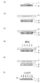
次に参照する図1(a)から図1(f)は、本実施形態に係る光重合性樹脂組成物を使用した微細構造体の製造方法を説明する工程図である。 Next, an embodiment of the present invention will be described in detail. Here, after explaining the manufacturing method of the microstructure using the photopolymerizable resin composition according to the present embodiment, the photopolymerizable resin composition will be explained.
Next, FIG. 1A to FIG. 1F to be referred to are process diagrams for explaining a method for manufacturing a microstructure using the photopolymerizable resin composition according to the present embodiment.
(微細構造体の製造方法)
この製造方法は、金型2(図1(b)参照)の凹凸パターンに対応する凹凸パターンを基板3(図1(a)参照)に形成した微細構造体5(図1(f)参照)を製造するものである。 (Manufacturing method of fine structure)
In this manufacturing method, a microstructure 5 (see FIG. 1 (f)) in which a concavo-convex pattern corresponding to the concavo-convex pattern of a mold 2 (see FIG. 1 (b)) is formed on a substrate 3 (see FIG. 1 (a)). Is to be manufactured.
図1(a)に示すように、この製造方法では、まず基板3の表面に後記する本発明の光重合性樹脂組成物1を付与する。付与する方法としては、特に制限はなく、例えば、マイクロピペットを使用して付与することができる。
この基板3としては、例えば、シリコン(ケイ素)、各種金属材料、ガラス、石英、セラミック、樹脂等が挙げられる。また、基板3は、その表面に金属層、樹脂層、酸化膜層等が形成された多層構造体であってもよい。また、基板3は、中心穴が加工されたものであってもよい。 As shown in FIG. 1A, in this manufacturing method, first, thephotopolymerizable resin composition 1 of the present invention described later is applied to the surface of the substrate 3. There is no restriction | limiting in particular as a method to provide, For example, it can provide using a micropipette.
Examples of thesubstrate 3 include silicon (silicon), various metal materials, glass, quartz, ceramic, and resin. The substrate 3 may be a multilayer structure having a metal layer, a resin layer, an oxide film layer, or the like formed on the surface thereof. Moreover, the board | substrate 3 may be a thing by which the center hole was processed.
この基板3としては、例えば、シリコン(ケイ素)、各種金属材料、ガラス、石英、セラミック、樹脂等が挙げられる。また、基板3は、その表面に金属層、樹脂層、酸化膜層等が形成された多層構造体であってもよい。また、基板3は、中心穴が加工されたものであってもよい。 As shown in FIG. 1A, in this manufacturing method, first, the
Examples of the
次に、図1(b)に示すように、基板3上で光重合性樹脂組成物1を広げることによって、基板3の表面には、光重合性樹脂組成物1からなる薄膜4が形成される。光重合性樹脂組成物1を広げる方法としては、公知の塗布方法を使用することができる。中でも、基板3を回転させることにより光重合性樹脂組成物1を遠心力で広げて薄膜4を形成するスピンコート法は、均一な厚さで薄膜4を形成することができるので特に好ましい。
なお、図1(b)中、符号2は、金型である。 Next, as shown in FIG. 1B, thethin film 4 made of the photopolymerizable resin composition 1 is formed on the surface of the substrate 3 by spreading the photopolymerizable resin composition 1 on the substrate 3. The As a method for spreading the photopolymerizable resin composition 1, a known coating method can be used. Among them, the spin coating method in which the thin film 4 is formed by spreading the photopolymerizable resin composition 1 by centrifugal force by rotating the substrate 3 is particularly preferable because the thin film 4 can be formed with a uniform thickness.
In addition, in FIG.1 (b), the code |symbol 2 is a metal mold | die.
なお、図1(b)中、符号2は、金型である。 Next, as shown in FIG. 1B, the
In addition, in FIG.1 (b), the code |
金型2は、その表面にナノメートル(nm)のサイズの凹凸パターンを有しており、本実施形態での凹凸パターンは、数十ナノメートルのサイズの微細パターンである。
この凹凸パターンの形成方法としては、例えばフォトリソグラフィ、集束イオンビームリソグラフィ、電子ビーム描画法、ナノプリント法等が挙げられる。これらの方法は、凹凸パターンの加工精度に応じて適宜に選択することができる。 Themold 2 has a concavo-convex pattern with a nanometer (nm) size on its surface, and the concavo-convex pattern in the present embodiment is a fine pattern with a size of several tens of nanometers.
Examples of the method for forming the concavo-convex pattern include photolithography, focused ion beam lithography, electron beam drawing, and nanoprinting. These methods can be appropriately selected according to the processing accuracy of the uneven pattern.
この凹凸パターンの形成方法としては、例えばフォトリソグラフィ、集束イオンビームリソグラフィ、電子ビーム描画法、ナノプリント法等が挙げられる。これらの方法は、凹凸パターンの加工精度に応じて適宜に選択することができる。 The
Examples of the method for forming the concavo-convex pattern include photolithography, focused ion beam lithography, electron beam drawing, and nanoprinting. These methods can be appropriately selected according to the processing accuracy of the uneven pattern.
金型2の材料としては、所定の強度を有し、要求される精度で凹凸パターン(微細パターン)を加工することができるものであれば特に制限はなく、例えば、シリコンウエハ、各種金属材料、ガラス、石英、セラミック、樹脂材料等が挙げられる。中でも、石英、Si、SiC、SiN、多結晶Si、Ni、Cr、Cu、光硬化性樹脂材料の硬化物等からなる金型2、及びこれらの2種以上を組み合わせた金型2は好ましい。
また、金型2の材料としては、後記するように、この金型2(図1(d)参照)を介して紫外光を薄膜4に照射する場合には、透明性を有する必要があり、特に、透明性が高い石英は好ましい。また、図1(d)において、基板3として透明性を有するものを使用し、この基板3側から薄膜4に紫外光を照射する場合には、金型2は、不透明な材料で形成することができる。
また、弾性変形可能な樹脂材料からなる金型2は、次の図1(c)に示すように、薄膜4に金型2を押し当てる際に、万一基板3の表面に異物(図示省略)が存在した場合にも、その異物の形状に応じて金型2が弾性変形することによって、異物の周辺で生じる金型2の非接触領域を最小限に止めることができるので好ましい。 The material of themold 2 is not particularly limited as long as it has a predetermined strength and can process a concavo-convex pattern (fine pattern) with a required accuracy. For example, a silicon wafer, various metal materials, Examples thereof include glass, quartz, ceramic, and resin material. Among these, a mold 2 made of quartz, Si, SiC, SiN, polycrystalline Si, Ni, Cr, Cu, a cured product of a photocurable resin material, or the like, and a mold 2 that is a combination of these two or more are preferable.
Moreover, as a material of themold 2, as will be described later, when the thin film 4 is irradiated with ultraviolet light through the mold 2 (see FIG. 1D), it is necessary to have transparency. In particular, quartz having high transparency is preferable. Further, in FIG. 1D, when a transparent substrate is used as the substrate 3 and the thin film 4 is irradiated with ultraviolet light from the substrate 3 side, the mold 2 is formed of an opaque material. Can do.
Further, as shown in FIG. 1C, themold 2 made of an elastically deformable resin material has a foreign object (not shown) on the surface of the substrate 3 when the mold 2 is pressed against the thin film 4. ) Is also preferable because the non-contact area of the mold 2 generated around the foreign substance can be minimized by elastically deforming the mold 2 according to the shape of the foreign substance.
また、金型2の材料としては、後記するように、この金型2(図1(d)参照)を介して紫外光を薄膜4に照射する場合には、透明性を有する必要があり、特に、透明性が高い石英は好ましい。また、図1(d)において、基板3として透明性を有するものを使用し、この基板3側から薄膜4に紫外光を照射する場合には、金型2は、不透明な材料で形成することができる。
また、弾性変形可能な樹脂材料からなる金型2は、次の図1(c)に示すように、薄膜4に金型2を押し当てる際に、万一基板3の表面に異物(図示省略)が存在した場合にも、その異物の形状に応じて金型2が弾性変形することによって、異物の周辺で生じる金型2の非接触領域を最小限に止めることができるので好ましい。 The material of the
Moreover, as a material of the
Further, as shown in FIG. 1C, the
次に、図1(c)に示すように、薄膜4に金型2が押し当てられることで、薄膜4には、金型2の凹凸パターンに対応する凹凸パターンが転写される。
Next, as shown in FIG. 1 (c), when the mold 2 is pressed against the thin film 4, the uneven pattern corresponding to the uneven pattern of the mold 2 is transferred to the thin film 4.
次に、この製造方法では、図1(d)に示すように、金型2の裏面(薄膜4の反対側の面)から紫外光(波長365nm)を薄膜4に照射することで、薄膜4を硬化させる。
Next, in this manufacturing method, as shown in FIG. 1D, the thin film 4 is irradiated with ultraviolet light (wavelength 365 nm) from the back surface of the mold 2 (surface opposite to the thin film 4). Is cured.
次に、図1(e)に示すように、薄膜4から金型2を剥離することで、金型2の凹凸パターンが転写された薄膜4を得る。そして、この薄膜4をレジスト膜として基板3にエッチングを施す。
Next, as shown in FIG. 1 (e), the mold 2 is peeled from the thin film 4 to obtain the thin film 4 to which the uneven pattern of the mold 2 is transferred. Then, the substrate 3 is etched using the thin film 4 as a resist film.
その結果、この製造方法では、図1(f)に示すように、基板3には、図1(e)の薄膜4の凸部をマスクとしてエッチングが施されることによって、金型2(図1(b)参照)の凹凸パターン(微細パターン)に対応する凹凸パターンを基板3に有する微細構造体5を得ることができる。
As a result, in this manufacturing method, as shown in FIG. 1 (f), the substrate 3 is etched using the convex portions of the thin film 4 in FIG. 1 (b)), a fine structure 5 having a concavo-convex pattern corresponding to the concavo-convex pattern (fine pattern) on the substrate 3 can be obtained.
(光重合性樹脂組成物)
本実施形態に係る光重合性樹脂組成物1(以下、符号は省略する)は、成分(A)としての6~15官能のアクリレートと、成分(B)としての重量平均分子量(Mw)が1000~10000のアクリレートと、成分(C)としてのベンゼン環を有するアクリレートと、成分(D)としての反応性希釈剤と、成分(E)としての光重合開始剤と、後記する所定の割合で含んで構成されている。 (Photopolymerizable resin composition)
Thephotopolymerizable resin composition 1 according to the present embodiment (hereinafter, the symbol is omitted) has a 6 to 15 functional acrylate as the component (A) and a weight average molecular weight (Mw) as the component (B) of 1000. ˜10000 acrylate, acrylate having a benzene ring as component (C), reactive diluent as component (D), photopolymerization initiator as component (E), in a predetermined ratio described later It consists of
本実施形態に係る光重合性樹脂組成物1(以下、符号は省略する)は、成分(A)としての6~15官能のアクリレートと、成分(B)としての重量平均分子量(Mw)が1000~10000のアクリレートと、成分(C)としてのベンゼン環を有するアクリレートと、成分(D)としての反応性希釈剤と、成分(E)としての光重合開始剤と、後記する所定の割合で含んで構成されている。 (Photopolymerizable resin composition)
The
<成分(A)>
6~15官能のアクリレートとしては、6~15のアクリル基を有するアクリレートモノマ又はオリゴマを挙げることができ、例えば、ジペンタエリスリトールヘキサアクリレート等が挙げられる。また、6~15官能のウレタンアクリレートやポリエステルアクリレート等を用いても良い。多官能ウレタンアクリレートは、アクリロイル基及び水酸基を有するアクリレートモノマとポリイソシアネートとのウレタン化反応で得られた化合物を用いることができる。
また、多官能ウレタンアクリレートは、市販品を用いることができ、例えばUV-1700B(日本合成化学社製、ウレタンアクリレートオリゴマ、6官能以上)、UA-53H(新中村化学社製、ウレタンアクリレートオリゴマ、15官能)、EBECRYL(登録商標)220(ダイセル・サイテック社製、ウレタンアクリレート、6官能)、UN-3320HA(根上工業社製、ウレタンアクリレート、6官能)が挙げられる。
また、多官能ポリエステルアクリレートは、市販品を用いることができ、例えば、EBECRYL1830(ダイセル・サイテック社製、ポリエステルアクリレートオリゴマ、6官能)、EBECRYL450(ダイセル・サイテック社製、ポリエステルアクリレートオリゴマ、6官能)等が挙げられる。 <Component (A)>
Examples of 6-15 functional acrylates include acrylate monomers or oligomers having 6-15 acrylic groups, such as dipentaerythritol hexaacrylate. Further, 6-15 functional urethane acrylate, polyester acrylate, or the like may be used. As the polyfunctional urethane acrylate, a compound obtained by a urethanization reaction between an acrylate monomer having an acryloyl group and a hydroxyl group and a polyisocyanate can be used.
As the polyfunctional urethane acrylate, commercially available products can be used. For example, UV-1700B (manufactured by Nippon Synthetic Chemical Co., Ltd., urethane acrylate oligomer, 6 functional or more), UA-53H (manufactured by Shin-Nakamura Chemical Co., Ltd., urethane acrylate oligomer, 15 functional), EBECRYL (registered trademark) 220 (manufactured by Daicel-Cytec, urethane acrylate, 6 functional), UN-3320HA (manufactured by Negami Kogyo Co., urethane acrylate, 6 functional).
Moreover, a commercial item can be used for polyfunctional polyester acrylate, for example, EBECRYL1830 (the Daicel-Cytec company make, polyester acrylate oligomer, 6 functionals), EBECRYL450 (Daicel-Cytech company make, polyester acrylate oligomer, 6 functionals) etc. Is mentioned.
成分(A)の光重合性樹脂組成物における割合は、0.5~10質量%となっている。このような範囲で成分(A)を含む光重合性樹脂組成物は、その薄膜4に金型2が押し当てられる際に(図1(c)参照)、凹凸パターン(微細パターン)の転写精度(成型精度)に優れることとなる。
The ratio of the component (A) in the photopolymerizable resin composition is 0.5 to 10% by mass. When the mold 2 is pressed against the thin film 4 (see FIG. 1 (c)), the photopolymerizable resin composition containing the component (A) within such a range has a transfer accuracy of the concavo-convex pattern (fine pattern). (Molding accuracy) will be excellent.
<成分(B)>
重量平均分子量(Mw)が1000~10000のアクリレートとしては、例えば、ポリ(メタ)アクリル酸メチル、エトキシ化ビスフェノールA型アクレート、芳香族ウレタンアクリレート、脂肪族ウレタンアクリレート、ポリエステルアクリレート等が挙げられる。市販品としては、例えば、EBECRYL8405(ダイセル・サイテック社製、ウレタンアクリレートオリゴマ、4官能、重量平均分子量(Mw)2700)、UV-7000B(日本合成化学社製、ウレタンアクリレートオリゴマ、2官能、重量平均分子量(Mw)5000)が挙げられる。これらの成分(B)としてのアクリレートは、2種以上を組み合わせて使用することができる。
また、成分(B)としては、前記した成分(A)のうち、重量平均分子量(Mw)が1000~10000のものを使用することもできる。 <Component (B)>
Examples of the acrylate having a weight average molecular weight (Mw) of 1000 to 10,000 include poly (meth) acrylate, ethoxylated bisphenol A acrylate, aromatic urethane acrylate, aliphatic urethane acrylate, polyester acrylate, and the like. Examples of commercially available products include EBECRYL8405 (manufactured by Daicel-Cytec, urethane acrylate oligomer, tetrafunctional, weight average molecular weight (Mw) 2700), UV-7000B (manufactured by Nippon Synthetic Chemical Co., Ltd., urethane acrylate oligomer, bifunctional, weight average). Molecular weight (Mw) 5000). These acrylates as component (B) can be used in combination of two or more.
As the component (B), a component having a weight average molecular weight (Mw) of 1000 to 10,000 among the components (A) described above can also be used.
成分(B)の光重合性樹脂組成物における割合は、0.5~10質量%となっている。このような範囲で成分(B)を含む光重合性樹脂組成物は、基板3上に薄膜4(図1(b)参照)を形成する際に優れた成膜性を発揮することとなる。
The ratio of the component (B) in the photopolymerizable resin composition is 0.5 to 10% by mass. The photopolymerizable resin composition containing the component (B) in such a range exhibits excellent film formability when the thin film 4 (see FIG. 1B) is formed on the substrate 3.
<成分(C)>
ベンゼン環を有するアクリレートとしては、アクリロイル基とベンゼン環を有するアクリレートモノマが用いられる。その具体例としては、例えば、フェノキシグリコールアクリレート、フェノキシエチレングリコールアクリレート、フェノキシポリエチレングリコールアクリレート、エトキシ化ビスフェノールAジアクリレート、プロポキシ化ビスフェノールAジアクリレート、ベンジルアクリレート等が挙げられる。 <Ingredient (C)>
As the acrylate having a benzene ring, an acrylate monomer having an acryloyl group and a benzene ring is used. Specific examples thereof include phenoxy glycol acrylate, phenoxy ethylene glycol acrylate, phenoxy polyethylene glycol acrylate, ethoxylated bisphenol A diacrylate, propoxylated bisphenol A diacrylate, and benzyl acrylate.
成分(C)の光重合性樹脂組成物における割合は、0.5~10質量%となっている。このような範囲で成分(C)を含む光重合性樹脂組成物は、図1(f)に示すように、硬化した薄膜4をレジスト膜として基板3にエッチングを施す際に、優れたエッチング耐性を発揮することとなる。
The proportion of component (C) in the photopolymerizable resin composition is 0.5 to 10% by mass. The photopolymerizable resin composition containing the component (C) within such a range has excellent etching resistance when etching the substrate 3 using the cured thin film 4 as a resist film, as shown in FIG. Will be demonstrated.
<成分(D)>
反応性希釈剤は、主に前記した成分(A)から成分(C)を希釈して光重合性樹脂組成物の粘度を低減するものである。この反応性希釈剤は、前記した成分(A)から成分(C)と架橋反応可能な官能基を有するものであれば特に制限はないが、単量体であることが望ましい。中でも、末端に(メタ)アクリレート基、ビニル基、エポキシ基及びオキセタニル基を少なくとも一つ有する単量体が望ましい。 <Component (D)>
The reactive diluent mainly reduces the viscosity of the photopolymerizable resin composition by diluting the component (C) from the component (A). The reactive diluent is not particularly limited as long as it has a functional group capable of undergoing a crosslinking reaction with the component (A) to the component (C), but is preferably a monomer. Among these, a monomer having at least one (meth) acrylate group, vinyl group, epoxy group, and oxetanyl group at the terminal is desirable.
反応性希釈剤としては、例えば、N-ビニルピロリドン、アクリロイルモルフォリン、N,N-ジメチルアクリルアミド、N-メチロールアクリルアミド、N,N-ジメチルアミノプロピルアクリルアミド、ビニル(メタ)アクリレート、アリル(メタ)アクリレート、メタアリル(メタ)アクリレート、アクリルグリシジルエーテル、アルキルフェノールモノグリシジルエーテル、アリルグリシジルエーテル、2-エチルヘキシルグリシジルエーテル、フェニルグリシジルエーテル、2-エチルヘキシルオキセタン等が挙げられる。これらの反応性希釈剤は、2種以上を組み合わせて使用することができる。
Examples of reactive diluents include N-vinylpyrrolidone, acryloylmorpholine, N, N-dimethylacrylamide, N-methylolacrylamide, N, N-dimethylaminopropylacrylamide, vinyl (meth) acrylate, allyl (meth) acrylate. Methallyl (meth) acrylate, acrylic glycidyl ether, alkylphenol monoglycidyl ether, allyl glycidyl ether, 2-ethylhexyl glycidyl ether, phenyl glycidyl ether, 2-ethylhexyl oxetane and the like. These reactive diluents can be used in combination of two or more.
以上のような反応性希釈剤の中でも、25℃の粘度が3mPa・s以下の(メタ)アクリレートが望ましい。
Among the reactive diluents as described above, (meth) acrylate having a viscosity at 25 ° C. of 3 mPa · s or less is desirable.
また、以上のような反応性希釈剤の中でも、単官能の(メタ)アクリレートが望ましい。
Of the reactive diluents described above, monofunctional (meth) acrylates are desirable.
また、25℃において揮発性を有するものが望ましく、更に具体的には、炭素数1~6の直鎖のアルキレン基を有する(メタ)アクリレートが望ましく、水素原子以外の置換基(例えば、アルキル基、水酸基等(但し、分岐してエーテルを構成することとなるアルコシキ基は除く))を分岐位置に有しないアルキレン基を有する(メタ)アクリレートが望ましい。
Further, those having volatility at 25 ° C. are desirable, more specifically, (meth) acrylates having a linear alkylene group having 1 to 6 carbon atoms are desirable, and substituents other than hydrogen atoms (for example, alkyl groups) (Meth) acrylates having an alkylene group that does not have a hydroxyl group or the like (however, except for an alkoxy group that is branched to form an ether) at the branching position are desirable.
このような望ましい反応性希釈剤としては、メチル(メタ)アクリレート、エチル(メタ)アクリレート、ブチル(メタ)アクリレート、ヘキシル(メタ)アクリレート、2-メトキシエチル(メタ)アクリレート、2-エトキシエチル(メタ)アクリレート、3-メトキシブチル(メタ)アクリレート、アリル(メタ)アクリレート、 及びシアノ(メタ)アクリレートが挙げられる。
Such desirable reactive diluents include methyl (meth) acrylate, ethyl (meth) acrylate, butyl (meth) acrylate, hexyl (meth) acrylate, 2-methoxyethyl (meth) acrylate, 2-ethoxyethyl (meth) ) Acrylate, 3-methoxybutyl (meth) acrylate, allyl (meth) acrylate, soot and cyano (meth) acrylate.
成分(D)の光重合性樹脂組成物における割合は、80~98質量%となっている。このような範囲で成分(D)を含む光重合性樹脂組成物は、図1(b)に示すように、基板3上に薄膜4を形成する際に、数十nmの厚さで薄膜4を形成すことができる。特に、前記した揮発性を有する反応性希釈剤は、基板3上に薄膜4を形成する際に、特にベーク処理を施さなくても、均一な薄膜4を形成することができる。
The proportion of component (D) in the photopolymerizable resin composition is 80 to 98% by mass. The photopolymerizable resin composition containing the component (D) in such a range has a thickness of several tens of nanometers when the thin film 4 is formed on the substrate 3 as shown in FIG. Can be formed. In particular, the reactive diluent having volatility described above can form a uniform thin film 4 without performing any baking process when the thin film 4 is formed on the substrate 3.
<成分(E)>
光反応開始剤としては、ラジカル重合開始剤が挙げられる。その具体例としては、例えば、1-ヒドロキシ-シクロヘキシル-フェニルケトン、2-ヒドロキシ-2-メチル-1-フェニル-プロパン-1-オン、1-[4-(2-ヒドロキシエトキシ)-フェニル]-2-ヒドロキシ-2-メチル-1-プロパン-1-オン、2-ヒドロキシ-1-{4-[4-(2-ヒドロキシ-2-メチル-プロピオニル)-ベンジル]フェニル}-2-メチル-プロパン-1-オン、2-メチル-1-(4-メチルチオフェニル)-2-モルフォリプロパン-1-オン、2-ベンジル-2-ジメチルアミノ-1-(4-モルフォリノフェニル)-ブタノン、1,2-(ジメチルアミノ)-2-[(4-メチルフェニル)メチル]-1-[4-(4-モルフォニル)フェニル]-1-ブタノン、2-(ジメチルアミノ)-2-[(4-メチルフェニル)メチル]-1-[4-(4-モルホリニル)フェニル]-1-ブタノン、2,4,6-トリメチルベンゾイル-ジフェニル-フォスフィンオキサイド、 ビス-(2,4,6-トリメチルベンゾイル)-フェニルフォスフィンオキサイド等が挙げられる。これらの光反応開始剤は2種以上を組み合わせて使用することができる。 <Ingredient (E)>
Examples of the photoreaction initiator include radical polymerization initiators. Specific examples thereof include, for example, 1-hydroxy-cyclohexyl-phenyl ketone, 2-hydroxy-2-methyl-1-phenyl-propan-1-one, 1- [4- (2-hydroxyethoxy) -phenyl]- 2-hydroxy-2-methyl-1-propan-1-one, 2-hydroxy-1- {4- [4- (2-hydroxy-2-methyl-propionyl) -benzyl] phenyl} -2-methyl-propane -1-one, 2-methyl-1- (4-methylthiophenyl) -2-morpholinpropan-1-one, 2-benzyl-2-dimethylamino-1- (4-morpholinophenyl) -butanone, , 2- (dimethylamino) -2-[(4-methylphenyl) methyl] -1- [4- (4-morpholinyl) phenyl] -1-butanone, 2- (dimethylamino C) -2-[(4-methylphenyl) methyl] -1- [4- (4-morpholinyl) phenyl] -1-butanone, 2,4,6-trimethylbenzoyl-diphenyl-phosphine oxide, bis- ( 2,4,6-trimethylbenzoyl) -phenylphosphine oxide and the like. These photoinitiators can be used in combination of two or more.
成分(E)の光重合性樹脂組成物における割合は、0.1~5質量%となっている。このような範囲で成分(E)を含む光重合性樹脂組成物は、図1(d)に示すように、薄膜4(光重合性樹脂組成物)に紫外光を照射された際に、速やかに硬化することができる。
The ratio of the component (E) in the photopolymerizable resin composition is 0.1 to 5% by mass. In such a range, the photopolymerizable resin composition containing the component (E), as shown in FIG. 1 (d), is promptly exposed when the thin film 4 (photopolymerizable resin composition) is irradiated with ultraviolet light. Can be cured.
以上のような本実施形態に係る光重合性樹脂組成物によれば、前記成分(A)から成分(E)を所定の割合で含むので、従来の光重合性樹脂組成物(例えば、特許文献1及び特許文献2参照)と比較して、より薄く均一な薄膜の形成が可能で、より微細化した微細パターンの転写精度に優れ、形成した薄膜の硬化時間が短く、従来よりもスループット性の向上した微細構造体を製造することができる微細構造転写用の光重合性樹脂組成物を提供することができる。
According to the photopolymerizable resin composition according to the present embodiment as described above, since the component (E) to the component (E) are contained at a predetermined ratio, the conventional photopolymerizable resin composition (for example, patent document) 1 and Patent Document 2), a thinner and more uniform thin film can be formed, transfer accuracy of a finer and finer pattern can be improved, and the curing time of the formed thin film is shorter, and the throughput performance is higher than the conventional one. It is possible to provide a photopolymerizable resin composition for fine structure transfer that can produce an improved fine structure.
また、以上のような本実施形態に係る光重合性樹脂組成物においては、前記成分(A)から前記成分(E)に加えて、更に、次に説明する成分(F)を含むことができる。
<成分(F)>
成分(F)は、25℃における粘度が12mPa・s以下の2官能アクリレートである。その具体例としては、例えば、ポリエチレングリコールジアクリレート、ポリプロピレングリコールジアクリレート、1,4-ブタンジオールジアクリレート、1,6-ヘキサンジオールジアクリレート、1,9-ノナンジオールジアクリレート、ネオペンチルグリコールジアクリレート等が挙げられる。
光重合性樹脂組成物における成分(A)の割合は、0.1~5質量%、成分(B)の割合は、0.5~10質量%、成分(C)の割合は、0.5~10質量%、成分(D)の割合は、80~98質量%、成分(E)の割合は、0.1~5質量%であると共に、成分(F)の割合は、0.5~10質量%である。
以上のような光重合性樹脂組成物によれば、前記した成分(A)から成分(E)を含む光重合性樹脂組成物が、従来の光重合性樹脂組成物よりも成膜性、速硬化性、及びパターン成型性に優れるところ、更に成分(F)を含むことによって、成膜性及び速硬化性をほとんど悪化させることなく、パターン成型性を更に向上する作用効果を奏することができる。 Moreover, in the photopolymerizable resin composition which concerns on this embodiment as mentioned above, in addition to the said component (E) from the said component (A), the component (F) demonstrated further can be included further. .
<Component (F)>
Component (F) is a bifunctional acrylate having a viscosity at 25 ° C. of 12 mPa · s or less. Specific examples thereof include, for example, polyethylene glycol diacrylate, polypropylene glycol diacrylate, 1,4-butanediol diacrylate, 1,6-hexanediol diacrylate, 1,9-nonanediol diacrylate, neopentyl glycol diacrylate. Etc.
The proportion of component (A) in the photopolymerizable resin composition is 0.1 to 5% by mass, the proportion of component (B) is 0.5 to 10% by mass, and the proportion of component (C) is 0.5%. 10% by mass, the proportion of component (D) is 80-98% by mass, the proportion of component (E) is 0.1-5% by mass, and the proportion of component (F) is 0.5- 10% by mass.
According to the photopolymerizable resin composition as described above, the photopolymerizable resin composition containing the component (A) to the component (E) described above is more film forming and faster than the conventional photopolymerizable resin composition. The place which is excellent in curability and pattern moldability, and by containing a component (F), there exists an effect which further improves pattern moldability, without making film-forming property and quick-curability hardly deteriorated.
また、以上のような成分(A)から成分(E)を含む光重合性樹脂組成物、及び更に成分(F)を含む光重合性樹脂組成物によれば、25℃の粘度が3mPa・s以下の(メタ)アクリレ-トからなる反応性希釈剤を含むことによって、更に薄く均一な薄膜の形成が可能になる。
Further, according to the photopolymerizable resin composition containing the component (A) to the component (E) and the photopolymerizable resin composition further containing the component (F), the viscosity at 25 ° C. is 3 mPa · s. By including a reactive diluent comprising the following (meth) acrylate, a thinner and more uniform thin film can be formed.
また、このような光重合性樹脂組成物によれば、単官能の(メタ)アクリレートからなる反応性希釈剤を含むことによって、紫外光を照射した際に、多官能の(メタ)アクリレートよりも短時間で薄膜を硬化させることができる。
Moreover, according to such a photopolymerizable resin composition, it contains a reactive diluent composed of a monofunctional (meth) acrylate, so that when irradiated with ultraviolet light, it is more than a polyfunctional (meth) acrylate. The thin film can be cured in a short time.
また、このような光重合性樹脂組成物によれば、揮発性の(メタ)アクリレートを含むことにより、更に具体的には炭素数1~6の直鎖のアルキレン基を有する(メタ)アクリレートを含むことにより、ベーク処理を行わずに基板上に均一な薄膜の形成が可能となる。
In addition, according to such a photopolymerizable resin composition, by including volatile (meth) acrylate, more specifically, (meth) acrylate having a linear alkylene group having 1 to 6 carbon atoms can be obtained. By including, a uniform thin film can be formed on the substrate without performing a baking process.
そして、以上のような光重合性樹脂組成物を使用して製造された微細構造体は、磁気記録媒体や光記録媒体等の情報記録媒体に適用可能である。またこの微細構造体は、大規模集積回路部品や、レンズ、偏光板、波長フィルタ、発光素子、光集積回路等の光学部品、免疫分析、DNA分離、細胞培養等のバイオデバイスへの適用が可能である。
And the fine structure manufactured using the above photopolymerizable resin composition is applicable to information recording media such as magnetic recording media and optical recording media. This microstructure can be applied to large-scale integrated circuit components, optical components such as lenses, polarizing plates, wavelength filters, light-emitting elements, and optical integrated circuits, and biodevices such as immunoanalysis, DNA separation, and cell culture. It is.
以上、本発明の実施形態について説明したが、本発明は前記実施形態に限定されず、種々の形態で実施することができる。
前記実施形態での微細構造体は、本実施形態に係る光重合性樹脂組成物からなる薄膜4を硬化させたものをレジスト膜としてエッチングされた基板で構成されるが、図1(e)に示す、凹凸パターン(微細パターン)が転写された薄膜4を基板3上で硬化したものを微細構造体として使用することができる。
また、前記実施形態に係る光重合性樹脂組成物は、必要に応じて、界面活性剤、重合禁止剤等の他の成分を含んでいてもよい。 As mentioned above, although embodiment of this invention was described, this invention is not limited to the said embodiment, It can implement with a various form.
The microstructure in the embodiment is composed of a substrate etched with a resist film made by curing thethin film 4 made of the photopolymerizable resin composition according to the present embodiment, as shown in FIG. The thin film 4 to which the uneven pattern (fine pattern) shown is cured on the substrate 3 can be used as the fine structure.
In addition, the photopolymerizable resin composition according to the embodiment may contain other components such as a surfactant and a polymerization inhibitor, if necessary.
前記実施形態での微細構造体は、本実施形態に係る光重合性樹脂組成物からなる薄膜4を硬化させたものをレジスト膜としてエッチングされた基板で構成されるが、図1(e)に示す、凹凸パターン(微細パターン)が転写された薄膜4を基板3上で硬化したものを微細構造体として使用することができる。
また、前記実施形態に係る光重合性樹脂組成物は、必要に応じて、界面活性剤、重合禁止剤等の他の成分を含んでいてもよい。 As mentioned above, although embodiment of this invention was described, this invention is not limited to the said embodiment, It can implement with a various form.
The microstructure in the embodiment is composed of a substrate etched with a resist film made by curing the
In addition, the photopolymerizable resin composition according to the embodiment may contain other components such as a surfactant and a polymerization inhibitor, if necessary.
次に、実施例を示しながら本発明の光重合性樹脂組成物を更に具体的に説明する。なお、以下の説明では光重合性樹脂組成物における各成分の組成[質量%]を単に[%]と略して記す。
(実施例1)
実施例1では、成分(A)から成分(E)を次の表1に示す組成[%]となるように混合し、次いで、この混合物を直径100nmの目開きのポリプロピレン製フィルタでろ過することによって、目的の光重合性樹脂組成物を得た。 Next, the photopolymerizable resin composition of the present invention will be described more specifically with reference to examples. In the following description, the composition [mass%] of each component in the photopolymerizable resin composition is simply abbreviated as [%].
Example 1
In Example 1, the components (A) to (E) are mixed so as to have the composition [%] shown in the following Table 1, and then the mixture is filtered through a polypropylene filter having a diameter of 100 nm. Thus, a desired photopolymerizable resin composition was obtained.

なお、成分(A)の「6~15官能のアクリレート」としては、6官能アクリレート(新中村化学社製、ジペンタエリスリトールヘキサアクリレート)を使用した。
成分(B)の「重量平均分子量(Mw)が1000~10000のアクリレート」としては、重量平均分子量(Mw)5000のアクリレート(日本合成化学社製、商品名UV-7000B、2~3官能ウレタンアクリレート)を使用した。
成分(C)の「ベンゼン環を有するアクリレート」としては、ベンジル基を有するアクリレート(日立化成工業社製、ベンジルアクリレート)を使用した。
成分(D)の「反応性希釈剤」としては、揮発性を有する反応性希釈剤(東京化成工業社製、ブチルアクリレート)を使用した。
成分(E)の「光重合開始剤」としては、ラジカル重合開始剤(チバ・ジャパン社製、IRGACURE(登録商標)369)を使用した。 As the “6-15 functional acrylate” of component (A), hexafunctional acrylate (manufactured by Shin-Nakamura Chemical Co., Ltd., dipentaerythritol hexaacrylate) was used.
As the component (B) “acrylate having a weight average molecular weight (Mw) of 1000 to 10,000”, an acrylate having a weight average molecular weight (Mw) of 5000 (manufactured by Nippon Synthetic Chemical Co., Ltd., trade name UV-7000B, bifunctional to trifunctional urethane acrylate) )It was used.
As the “acrylate having a benzene ring” as the component (C), an acrylate having a benzyl group (manufactured by Hitachi Chemical Co., Ltd., benzyl acrylate) was used.
As the “reactive diluent” of component (D), a reactive diluent having a volatility (Butyl acrylate, manufactured by Tokyo Chemical Industry Co., Ltd.) was used.
As the “photopolymerization initiator” of component (E), a radical polymerization initiator (manufactured by Ciba Japan, IRGACURE (registered trademark) 369) was used.
次に本実施例で調製した光重合性樹脂組成物を使用して、図1(a)から(f)に示す工程で、微細構造体5(図1(f)参照)を作製した。
図1(a)に示す基板3としては、厚さが0.625mm、直径が65mmのシリコン(Si)ウエハを使用した。
本実施例では、図1(a)に示すように、光重合性樹脂組成物1を、マイクロピペットを用いて500μL滴下した。 Next, by using the photopolymerizable resin composition prepared in this example, a microstructure 5 (see FIG. 1 (f)) was produced in the steps shown in FIGS. 1 (a) to (f).
As thesubstrate 3 shown in FIG. 1A, a silicon (Si) wafer having a thickness of 0.625 mm and a diameter of 65 mm was used.
In this example, as shown in FIG. 1A, 500 μL of thephotopolymerizable resin composition 1 was dropped using a micropipette.
図1(a)に示す基板3としては、厚さが0.625mm、直径が65mmのシリコン(Si)ウエハを使用した。
本実施例では、図1(a)に示すように、光重合性樹脂組成物1を、マイクロピペットを用いて500μL滴下した。 Next, by using the photopolymerizable resin composition prepared in this example, a microstructure 5 (see FIG. 1 (f)) was produced in the steps shown in FIGS. 1 (a) to (f).
As the
In this example, as shown in FIG. 1A, 500 μL of the
次に、基板3上に滴下した光重合性樹脂組成物1をスピンコート法によって広げて、図1(b)に示す薄膜4を形成した。スピンコート法は、回転速度5000rpm、回転時間60秒間の条件で行った。そして、形成した薄膜4の面内における12点について薄膜4の厚さをエリプソメーターで測定した。その結果、薄膜4の厚さは、45±2nmの範囲で均一な膜が形成されていることが確認された。
Next, the photopolymerizable resin composition 1 dropped on the substrate 3 was spread by a spin coating method to form a thin film 4 shown in FIG. The spin coating method was performed under conditions of a rotation speed of 5000 rpm and a rotation time of 60 seconds. And the thickness of the thin film 4 was measured with the ellipsometer about 12 points in the surface of the formed thin film 4. As a result, it was confirmed that the thin film 4 had a uniform thickness in the range of 45 ± 2 nm.
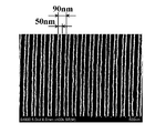
次に、図1(c)に示すように、金型2を薄膜4に押し当てて、金型2の凹凸パターン(微細パターン)を薄膜4に転写した。金型2としては、厚さが0.7mm、直径が150mmの円形の石英製のものを使用した。この金型2の凹凸パターン(微細パターン)は、金型2の内径30mmから60mmのリング状の領域に、同心円状のラインアンドスペースが繰り返して形成されたパターン(ライン幅50nm、ピッチ90nm、高さ40nm)であった。なお、金型2は、0.2MPaの圧力で薄膜4に押し当てられた。
Next, as shown in FIG. 1 (c), the mold 2 was pressed against the thin film 4 to transfer the uneven pattern (fine pattern) of the mold 2 to the thin film 4. As the mold 2, a circular quartz product having a thickness of 0.7 mm and a diameter of 150 mm was used. The concave / convex pattern (fine pattern) of the mold 2 is a pattern (line width 50 nm, pitch 90 nm, 40 nm). The mold 2 was pressed against the thin film 4 with a pressure of 0.2 MPa.
次に、図1(d)に示すように、所定の紫外線ランプ(図示省略)を使用して紫外光(波長365nm)を、金型2を介して薄膜4に照射することによって、光重合性樹脂組成物1(図1(a)参照)からなる薄膜4を硬化させた。
なお、薄膜4は、紫外線照射量が100mJ/cm2、つまり所定の出力の紫外線ランプを使用した場合に、通常よりも僅かな照射量(照射時間)で硬化できることが確認された。 Next, as shown in FIG. 1 (d), the photopolymerizability is obtained by irradiating thethin film 4 with ultraviolet light (wavelength 365 nm) through a mold 2 using a predetermined ultraviolet lamp (not shown). The thin film 4 made of the resin composition 1 (see FIG. 1A) was cured.
In addition, it was confirmed that thethin film 4 can be cured with an irradiation amount (irradiation time) slightly smaller than usual when an ultraviolet ray irradiation amount of 100 mJ / cm 2 , that is, a predetermined output ultraviolet lamp is used.
なお、薄膜4は、紫外線照射量が100mJ/cm2、つまり所定の出力の紫外線ランプを使用した場合に、通常よりも僅かな照射量(照射時間)で硬化できることが確認された。 Next, as shown in FIG. 1 (d), the photopolymerizability is obtained by irradiating the
In addition, it was confirmed that the
そして、図1(e)に示すように、硬化した薄膜4から金型2を剥離することによって、金型2の凹凸パターン(微細パターン)が転写された薄膜4を得た。次いで、薄膜4の表面をSEMで観察したところ、その表面には、ライン幅50nm、及びピッチ90nmで同心円状に形成されたラインアンドスペースからなる凹凸パターン(微細パターン)が確認された。図2は、実施例1の光重合性樹脂組成物からなる薄膜の表面に形成された凹凸パターン(微細パターン)のSEM写真である。
And as shown in FIG.1 (e), the thin film 4 to which the uneven | corrugated pattern (fine pattern) of the metal mold | die 2 was transcribe | transferred by peeling the metal mold | die 2 from the hardened thin film 4 was obtained. Next, when the surface of the thin film 4 was observed with an SEM, a concavo-convex pattern (fine pattern) composed of lines and spaces formed concentrically with a line width of 50 nm and a pitch of 90 nm was confirmed on the surface. FIG. 2 is an SEM photograph of a concavo-convex pattern (fine pattern) formed on the surface of a thin film made of the photopolymerizable resin composition of Example 1.
次に、図1(f)に示すように、凹凸パターン(微細パターン)が転写された薄膜4をレジスト膜として、基板3にエッチングを施すことによって、微細構造体5を得た。なお、この際、基板3の表面が露出するまでは、酸素プラズマによるエッチングを行い、その後、酸素プラズマに代えてフッ素系ガスプラズマによるエッチングを行って微細構造体5を得た。次いで、微細構造体5の表面をSEMで観察したところ、図2に示すように、その表面には、ライン幅50nm、及びピッチ90nmで同心円状に形成された。つまり、光重合性樹脂組成物1(図1(a)参照)が硬化して形成された薄膜4は、十分なエッチング耐性を示すことが確認された。
Next, as shown in FIG. 1 (f), the microstructure 3 was obtained by etching the substrate 3 using the thin film 4 to which the concavo-convex pattern (fine pattern) was transferred as a resist film. At this time, etching with oxygen plasma was performed until the surface of the substrate 3 was exposed, and then etching with fluorine-based gas plasma was performed in place of oxygen plasma to obtain the microstructure 5. Next, when the surface of the fine structure 5 was observed by SEM, as shown in FIG. 2, the surface was formed concentrically with a line width of 50 nm and a pitch of 90 nm. That is, it was confirmed that the thin film 4 formed by curing the photopolymerizable resin composition 1 (see FIG. 1A) exhibits sufficient etching resistance.
以上のような本実施例での光重合性樹脂組成物1(図1(a)参照)について、次の成膜性、硬化性、及び転写精度について評価を行った。
<成膜性>
図1(b)に示す工程で、基板3上に形成された薄膜4の面内における12点について薄膜4の厚さを測定し、50nm以下の均一な薄膜4が形成されたものについて「良」と評価し、形成されなかったものを「不良」と評価した。その結果を表1に示す。
<硬化性>
図1(d)に示す工程で、紫外光(波長365nm)を、金型2を介して薄膜4に照射した際に、照射量が200mJ/cm2以内で薄膜4が硬化したものを、通常よりも僅かな照射量(照射時間)で硬化できると判定して「良」と評価し、200mJ/cm2以内で薄膜4が硬化しなかったものを、通常と同等かそれ以下と判定し、「不良」と評価した。その結果を表1に示す。
<転写精度>
図1(e)に示す工程で、前記した同心円状のパターン(ライン幅50nm、ピッチ90nm、高さ40nm)が薄膜4に転写することができたものを「良」と判定し、転写できなかったものを「不良」と判定した。その結果を表1に示す。 About the photopolymerizable resin composition 1 (refer FIG. 1 (a)) in the above Examples, the following film-forming property, sclerosis | hardenability, and transfer precision were evaluated.
<Film forming properties>
In the step shown in FIG. 1B, the thickness of thethin film 4 is measured at 12 points in the plane of the thin film 4 formed on the substrate 3, and the film having a uniform thin film 4 of 50 nm or less is formed as “good”. ”And those not formed were evaluated as“ bad ”. The results are shown in Table 1.
<Curing property>
In the step shown in FIG. 1D, when thethin film 4 is irradiated with ultraviolet light (wavelength 365 nm) through the mold 2, the irradiation amount is within 200 mJ / cm 2 and the thin film 4 is usually cured. It is determined that it can be cured with a smaller dose (irradiation time) than "evaluated", and the thin film 4 is not cured within 200 mJ / cm 2 is determined to be equal to or less than normal, Rated as “bad”. The results are shown in Table 1.
<Transfer accuracy>
In the step shown in FIG. 1E, the above-mentioned concentric pattern (line width 50 nm, pitch 90 nm, height 40 nm) was transferred to thethin film 4 as “good” and could not be transferred. Was judged as “bad”. The results are shown in Table 1.
<成膜性>
図1(b)に示す工程で、基板3上に形成された薄膜4の面内における12点について薄膜4の厚さを測定し、50nm以下の均一な薄膜4が形成されたものについて「良」と評価し、形成されなかったものを「不良」と評価した。その結果を表1に示す。
<硬化性>
図1(d)に示す工程で、紫外光(波長365nm)を、金型2を介して薄膜4に照射した際に、照射量が200mJ/cm2以内で薄膜4が硬化したものを、通常よりも僅かな照射量(照射時間)で硬化できると判定して「良」と評価し、200mJ/cm2以内で薄膜4が硬化しなかったものを、通常と同等かそれ以下と判定し、「不良」と評価した。その結果を表1に示す。
<転写精度>
図1(e)に示す工程で、前記した同心円状のパターン(ライン幅50nm、ピッチ90nm、高さ40nm)が薄膜4に転写することができたものを「良」と判定し、転写できなかったものを「不良」と判定した。その結果を表1に示す。 About the photopolymerizable resin composition 1 (refer FIG. 1 (a)) in the above Examples, the following film-forming property, sclerosis | hardenability, and transfer precision were evaluated.
<Film forming properties>
In the step shown in FIG. 1B, the thickness of the
<Curing property>
In the step shown in FIG. 1D, when the
<Transfer accuracy>
In the step shown in FIG. 1E, the above-mentioned concentric pattern (line width 50 nm, pitch 90 nm, height 40 nm) was transferred to the
(実施例2)
実施例2では、成分(A)として、6官能アクリレートに代えて、15官能アクリレート(新中村化学社製、ウレタンアクリレートオリゴマ、商品名UA-53H)を使用した以外は、実施例1と同様にして光重合性樹脂組成物を調製し、この光重合性樹脂組成物を使用して微細構造体5(図1(f)参照)を得た。この際、光重合性樹脂組成物が硬化して形成された薄膜4(図1(e)参照)は、十分なエッチング耐性を示すことが確認された。
そして、本実施例で得られた光重合性樹脂組成物について、成膜性、硬化性、及び転写精度を実施例1と同様にして評価した。その結果を表1に示す。 (Example 2)
Example 2 was the same as Example 1 except that instead of 6-functional acrylate, 15-functional acrylate (manufactured by Shin-Nakamura Chemical Co., Ltd., urethane acrylate oligomer, trade name UA-53H) was used as component (A). Thus, a photopolymerizable resin composition was prepared, and a microstructure 5 (see FIG. 1 (f)) was obtained using this photopolymerizable resin composition. At this time, it was confirmed that the thin film 4 (see FIG. 1E) formed by curing the photopolymerizable resin composition exhibits sufficient etching resistance.
The film-forming property, curability, and transfer accuracy of the photopolymerizable resin composition obtained in this example were evaluated in the same manner as in Example 1. The results are shown in Table 1.
(実施例3)
実施例3では、成分(B)として、重量平均分子量(Mw)2700のアクリレートに代えて、重量平均分子量(Mw)5000のアクリレート(日本合成化学社製、ウレタンアクリレートオリゴマ、商品名UV-7000B)を使用した以外は、実施例1と同様にして光重合性樹脂組成物を調製し、この光重合性樹脂組成物を使用して微細構造体5(図1(f)参照)を得た。この際、光重合性樹脂組成物が硬化して形成された薄膜4(図1(e)参照)は、十分なエッチング耐性を示すことが確認された。
そして、本実施例で得られた光重合性樹脂組成物について、成膜性、硬化性、及び転写精度を実施例1と同様にして評価した。その結果を表1に示す。 (Example 3)
In Example 3, as an ingredient (B), an acrylate having a weight average molecular weight (Mw) of 5000 instead of an acrylate having a weight average molecular weight (Mw) of 2700 (manufactured by Nippon Synthetic Chemical Co., Ltd., urethane acrylate oligomer, trade name UV-7000B) A photopolymerizable resin composition was prepared in the same manner as in Example 1 except that was used, and a microstructure 5 (see FIG. 1 (f)) was obtained using this photopolymerizable resin composition. At this time, it was confirmed that the thin film 4 (see FIG. 1E) formed by curing the photopolymerizable resin composition exhibits sufficient etching resistance.
The film-forming property, curability, and transfer accuracy of the photopolymerizable resin composition obtained in this example were evaluated in the same manner as in Example 1. The results are shown in Table 1.
(実施例4)
実施例4では、成分(D)として、ブチルアクリレートに代えて、揮発性を有する2-メトキシエチルアクリレート(東京化成工業社製)を使用すると共に、成分(A)から成分(E)を表1に示す組成[%]とした以外は、実施例1と同様にして光重合性樹脂組成物を調製し、この光重合性樹脂組成物を使用して微細構造体5(図1(f)参照)を得た。この際、光重合性樹脂組成物が硬化して形成された薄膜4(図1(e)参照)は、十分なエッチング耐性を示すことが確認された。
そして、本実施例で得られた光重合性樹脂組成物について、成膜性、硬化性、及び転写精度を実施例1と同様にして評価した。その結果を表1に示す。 Example 4
In Example 4, volatile 2-methoxyethyl acrylate (manufactured by Tokyo Chemical Industry Co., Ltd.) was used as the component (D) instead of butyl acrylate, and the components (A) to (E) were changed from Table 1 A photopolymerizable resin composition was prepared in the same manner as in Example 1 except that the composition [%] shown in FIG. 1 was used, and the microstructure 5 (see FIG. 1 (f)) was prepared using this photopolymerizable resin composition. ) At this time, it was confirmed that the thin film 4 (see FIG. 1E) formed by curing the photopolymerizable resin composition exhibits sufficient etching resistance.
The film-forming property, curability, and transfer accuracy of the photopolymerizable resin composition obtained in this example were evaluated in the same manner as in Example 1. The results are shown in Table 1.
(実施例5)
実施例5では、成分(A)から成分(F)を表1に示す組成[%]となるように混合し、次いで、この混合物を直径100nmの目開きのポリプロピレン製フィルタでろ過することによって、目的の光重合性樹脂組成物を得た。 (Example 5)
In Example 5, the components (A) to (F) were mixed so as to have the composition [%] shown in Table 1, and the mixture was then filtered through a polypropylene filter having an opening of 100 nm in diameter. The intended photopolymerizable resin composition was obtained.
なお、成分(A)の「6~15官能のアクリレート」としては、6官能アクリレート(新中村化学社製、ジペンタエリスリトールエトキシレートヘキサアクリレート)を使用した。
成分(B)の「重量平均分子量(Mw)が1000~10000のアクリレート」としては、重量平均分子量(Mw)5000のアクリレート(日本合成化学社製、商品名UV-3000B、2官能ウレタンアクリレート)を使用した。
成分(C)の「ベンゼン環を有するアクリレート」としては、ベンジル基を有するアクリレート(日立化成工業社製、ベンジルアクリレート)を使用した。
成分(D)の「反応性希釈剤」としては、揮発性を有する反応性希釈剤(東京化成工業社製、ブチルアクリレート)を使用した。
成分(E)の「光重合開始剤」としては、ラジカル重合開始剤(チバ・ジャパン社製、IRGACURE(登録商標)369)を使用した。
成分(F)の「25℃における粘度が12mPa・s以下の2官能アクリレート」としては、1,4-ブタンジオールジアクリレート(東京化成工業社製)を使用した。
そして、本実施例で得られた光重合性樹脂組成物について、成膜性、硬化性、及び転写精度を実施例1と同様にして評価した。その結果を表1に示す。 As the “6-15 functional acrylate” of component (A), hexafunctional acrylate (manufactured by Shin-Nakamura Chemical Co., Ltd., dipentaerythritol ethoxylate hexaacrylate) was used.
As the “acrylate having a weight average molecular weight (Mw) of 1000 to 10,000” as the component (B), an acrylate having a weight average molecular weight (Mw) of 5000 (manufactured by Nippon Synthetic Chemical Co., Ltd., trade name UV-3000B, bifunctional urethane acrylate) is used. used.
As the “acrylate having a benzene ring” as the component (C), an acrylate having a benzyl group (manufactured by Hitachi Chemical Co., Ltd., benzyl acrylate) was used.
As the “reactive diluent” of component (D), a reactive diluent having a volatility (Butyl acrylate, manufactured by Tokyo Chemical Industry Co., Ltd.) was used.
As the “photopolymerization initiator” of component (E), a radical polymerization initiator (manufactured by Ciba Japan, IRGACURE (registered trademark) 369) was used.
As the component (F) “bifunctional acrylate having a viscosity at 25 ° C. of 12 mPa · s or less”, 1,4-butanediol diacrylate (manufactured by Tokyo Chemical Industry Co., Ltd.) was used.
The film-forming property, curability, and transfer accuracy of the photopolymerizable resin composition obtained in this example were evaluated in the same manner as in Example 1. The results are shown in Table 1.
(比較例1)
比較例1では、成分(C)及び成分(D)の配合を、表1に示すように変更した組成とした以外は、実施例1と同様にして光重合性樹脂組成物を調製した。そして、この光重合性樹脂組成物を使用して実施例1と同様に、スピンコート法によって図1(b)に示す薄膜4を形成しようとしたところ、薄膜4の厚さは、500nm以上となった。
したがって、比較例1の光重合性樹脂組成物における成膜性の評価結果は、表1に示すように、「不良」とした。
なお、比較例1の光重合性樹脂組成物では、成膜性が「不良」と評価されたことから、硬化性及び転写精度の評価は行わなかった。 (Comparative Example 1)
In Comparative Example 1, a photopolymerizable resin composition was prepared in the same manner as in Example 1 except that the composition of Component (C) and Component (D) was changed as shown in Table 1. And when it tried to form thethin film 4 shown in FIG.1 (b) by the spin coat method using this photopolymerizable resin composition similarly to Example 1, the thickness of the thin film 4 was 500 nm or more. became.
Therefore, as shown in Table 1, the evaluation result of the film formability in the photopolymerizable resin composition of Comparative Example 1 was “bad”.
In addition, in the photopolymerizable resin composition of Comparative Example 1, since the film formability was evaluated as “poor”, the curability and the transfer accuracy were not evaluated.
比較例1では、成分(C)及び成分(D)の配合を、表1に示すように変更した組成とした以外は、実施例1と同様にして光重合性樹脂組成物を調製した。そして、この光重合性樹脂組成物を使用して実施例1と同様に、スピンコート法によって図1(b)に示す薄膜4を形成しようとしたところ、薄膜4の厚さは、500nm以上となった。
したがって、比較例1の光重合性樹脂組成物における成膜性の評価結果は、表1に示すように、「不良」とした。
なお、比較例1の光重合性樹脂組成物では、成膜性が「不良」と評価されたことから、硬化性及び転写精度の評価は行わなかった。 (Comparative Example 1)
In Comparative Example 1, a photopolymerizable resin composition was prepared in the same manner as in Example 1 except that the composition of Component (C) and Component (D) was changed as shown in Table 1. And when it tried to form the
Therefore, as shown in Table 1, the evaluation result of the film formability in the photopolymerizable resin composition of Comparative Example 1 was “bad”.
In addition, in the photopolymerizable resin composition of Comparative Example 1, since the film formability was evaluated as “poor”, the curability and the transfer accuracy were not evaluated.
(比較例2)
比較例2では、成分(A)として、6官能アクリレートに代えて、表1中、成分(A)´として示す、2官能アクリレート(東京化成工業社製、1,4-ブタンジオールジアクリレート)を使用した以外は、実施例1と同様にして光重合性樹脂組成物を調製し、図1(e)に示す、凹凸パターン(微細パターン)を転写した薄膜4を得た。
この際、比較例2の光重合性樹脂組成物における成膜性及び硬化性は良好であり、評価結果は表1に示すように「良」とした。
また、凹凸パターン(微細パターン)を転写した薄膜4の表面をSEMで観察したところ、その表面には、部分的にラインアンドスペースが欠損する凹凸パターン(微細パターン)が確認された。したがって、比較例2の光重合性樹脂組成物における転写精度の評価結果は、表1に示すように、「不良」とした。 (Comparative Example 2)
In Comparative Example 2, a bifunctional acrylate (manufactured by Tokyo Chemical Industry Co., Ltd., 1,4-butanediol diacrylate) shown as a component (A) ′ in Table 1 was used instead of the hexafunctional acrylate as the component (A). A photopolymerizable resin composition was prepared in the same manner as in Example 1 except that it was used, and athin film 4 having a concavo-convex pattern (fine pattern) transferred as shown in FIG.
At this time, the film formability and curability of the photopolymerizable resin composition of Comparative Example 2 were good, and the evaluation result was “good” as shown in Table 1.
Moreover, when the surface of thethin film 4 which transferred the uneven | corrugated pattern (fine pattern) was observed by SEM, the uneven | corrugated pattern (fine pattern) in which a line and space partly lost was confirmed on the surface. Therefore, as shown in Table 1, the evaluation result of the transfer accuracy in the photopolymerizable resin composition of Comparative Example 2 was “bad”.
比較例2では、成分(A)として、6官能アクリレートに代えて、表1中、成分(A)´として示す、2官能アクリレート(東京化成工業社製、1,4-ブタンジオールジアクリレート)を使用した以外は、実施例1と同様にして光重合性樹脂組成物を調製し、図1(e)に示す、凹凸パターン(微細パターン)を転写した薄膜4を得た。
この際、比較例2の光重合性樹脂組成物における成膜性及び硬化性は良好であり、評価結果は表1に示すように「良」とした。
また、凹凸パターン(微細パターン)を転写した薄膜4の表面をSEMで観察したところ、その表面には、部分的にラインアンドスペースが欠損する凹凸パターン(微細パターン)が確認された。したがって、比較例2の光重合性樹脂組成物における転写精度の評価結果は、表1に示すように、「不良」とした。 (Comparative Example 2)
In Comparative Example 2, a bifunctional acrylate (manufactured by Tokyo Chemical Industry Co., Ltd., 1,4-butanediol diacrylate) shown as a component (A) ′ in Table 1 was used instead of the hexafunctional acrylate as the component (A). A photopolymerizable resin composition was prepared in the same manner as in Example 1 except that it was used, and a
At this time, the film formability and curability of the photopolymerizable resin composition of Comparative Example 2 were good, and the evaluation result was “good” as shown in Table 1.
Moreover, when the surface of the
(比較例3)
比較例3では、成分(A)として、6官能アクリレートに代えて、表1中、成分(A)´として示す、2官能アクリレート(東京化成工業社製、1,4-ブタンジオールジアクリレート)を10%使用すると共に、成分(B)から成分(E)を表1に示す組成[%]とした以外は、実施例1と同様にして光重合性樹脂組成物を調製した。そして、この光重合性樹脂組成物を使用して実施例1と同様に、スピンコート法によって図1(b)に示す薄膜4を形成しようとしたところ、薄膜4の厚さは、200nm以上となった。
したがって、比較例1の光重合性樹脂組成物における成膜性の評価結果は、表1に示すように、「不良」とした。
なお、比較例1の光重合性樹脂組成物では、成膜性が「不良」と評価されたことから、硬化性及び転写精度の評価は行わなかった。 (Comparative Example 3)
In Comparative Example 3, a bifunctional acrylate (manufactured by Tokyo Chemical Industry Co., Ltd., 1,4-butanediol diacrylate) shown as a component (A) ′ in Table 1 was used instead of the hexafunctional acrylate as the component (A). A photopolymerizable resin composition was prepared in the same manner as in Example 1 except that 10% was used and the component (B) to component (E) were changed to the composition [%] shown in Table 1. And when it tried to form thethin film 4 shown in FIG.1 (b) by the spin coat method using this photopolymerizable resin composition like Example 1, the thickness of the thin film 4 was 200 nm or more. became.
Therefore, as shown in Table 1, the evaluation result of the film formability in the photopolymerizable resin composition of Comparative Example 1 was “bad”.
In addition, in the photopolymerizable resin composition of Comparative Example 1, since the film formability was evaluated as “poor”, the curability and the transfer accuracy were not evaluated.
比較例3では、成分(A)として、6官能アクリレートに代えて、表1中、成分(A)´として示す、2官能アクリレート(東京化成工業社製、1,4-ブタンジオールジアクリレート)を10%使用すると共に、成分(B)から成分(E)を表1に示す組成[%]とした以外は、実施例1と同様にして光重合性樹脂組成物を調製した。そして、この光重合性樹脂組成物を使用して実施例1と同様に、スピンコート法によって図1(b)に示す薄膜4を形成しようとしたところ、薄膜4の厚さは、200nm以上となった。
したがって、比較例1の光重合性樹脂組成物における成膜性の評価結果は、表1に示すように、「不良」とした。
なお、比較例1の光重合性樹脂組成物では、成膜性が「不良」と評価されたことから、硬化性及び転写精度の評価は行わなかった。 (Comparative Example 3)
In Comparative Example 3, a bifunctional acrylate (manufactured by Tokyo Chemical Industry Co., Ltd., 1,4-butanediol diacrylate) shown as a component (A) ′ in Table 1 was used instead of the hexafunctional acrylate as the component (A). A photopolymerizable resin composition was prepared in the same manner as in Example 1 except that 10% was used and the component (B) to component (E) were changed to the composition [%] shown in Table 1. And when it tried to form the
Therefore, as shown in Table 1, the evaluation result of the film formability in the photopolymerizable resin composition of Comparative Example 1 was “bad”.
In addition, in the photopolymerizable resin composition of Comparative Example 1, since the film formability was evaluated as “poor”, the curability and the transfer accuracy were not evaluated.
(比較例4)
比較例4では、成分(B)として、重量平均分子量(Mw)2700のアクリレートに代えて、表1中、成分(B)´として示す、重量平均分子量(Mw)500のアクリレート(ダイセル・サイテック社製、商品名EBECRYL600、2官能ビスフェノールAエポキシアクリレート)を使用した以外は、実施例1と同様にして光重合性樹脂組成物を調製した。そして、この光重合性樹脂組成物を使用して実施例1と同様に、スピンコート法によって図1(b)に示す薄膜4を形成しようとしたところ、基板3上で広がった薄膜4は、時間経過と共に表面張力によって収縮し、膜を維持することができなかった。
したがって、比較例1の光重合性樹脂組成物における成膜性の評価結果は、表1に示すように、「不良」とした。
なお、比較例1の光重合性樹脂組成物では、成膜性が「不良」と評価されたことから、硬化性及び転写精度の評価は行わなかった。 (Comparative Example 4)
In Comparative Example 4, as the component (B), an acrylate having a weight average molecular weight (Mw) of 500 shown as a component (B) ′ in Table 1 instead of an acrylate having a weight average molecular weight (Mw) of 2700 (Daicel Cytec Co., Ltd.) A photopolymerizable resin composition was prepared in the same manner as in Example 1 except that the product name EBECRYL600, bifunctional bisphenol A epoxy acrylate) was used. And when it was going to form thethin film 4 shown in FIG.1 (b) by the spin coat method using this photopolymerizable resin composition like Example 1, the thin film 4 spread on the substrate 3 was: The film contracted due to surface tension over time, and the film could not be maintained.
Therefore, as shown in Table 1, the evaluation result of the film formability in the photopolymerizable resin composition of Comparative Example 1 was “bad”.
In addition, in the photopolymerizable resin composition of Comparative Example 1, since the film formability was evaluated as “poor”, the curability and the transfer accuracy were not evaluated.
比較例4では、成分(B)として、重量平均分子量(Mw)2700のアクリレートに代えて、表1中、成分(B)´として示す、重量平均分子量(Mw)500のアクリレート(ダイセル・サイテック社製、商品名EBECRYL600、2官能ビスフェノールAエポキシアクリレート)を使用した以外は、実施例1と同様にして光重合性樹脂組成物を調製した。そして、この光重合性樹脂組成物を使用して実施例1と同様に、スピンコート法によって図1(b)に示す薄膜4を形成しようとしたところ、基板3上で広がった薄膜4は、時間経過と共に表面張力によって収縮し、膜を維持することができなかった。
したがって、比較例1の光重合性樹脂組成物における成膜性の評価結果は、表1に示すように、「不良」とした。
なお、比較例1の光重合性樹脂組成物では、成膜性が「不良」と評価されたことから、硬化性及び転写精度の評価は行わなかった。 (Comparative Example 4)
In Comparative Example 4, as the component (B), an acrylate having a weight average molecular weight (Mw) of 500 shown as a component (B) ′ in Table 1 instead of an acrylate having a weight average molecular weight (Mw) of 2700 (Daicel Cytec Co., Ltd.) A photopolymerizable resin composition was prepared in the same manner as in Example 1 except that the product name EBECRYL600, bifunctional bisphenol A epoxy acrylate) was used. And when it was going to form the
Therefore, as shown in Table 1, the evaluation result of the film formability in the photopolymerizable resin composition of Comparative Example 1 was “bad”.
In addition, in the photopolymerizable resin composition of Comparative Example 1, since the film formability was evaluated as “poor”, the curability and the transfer accuracy were not evaluated.
(比較例5)
比較例5では、成分(C)として、フェノキシ基を有するアクリレートに代えて、表1中、成分(C)´として示す、アクリレートではないベンジルメタクリレート(日立化成工業社製)を使用した以外は、実施例1と同様にして光重合性樹脂組成物を調製し、図1(b)に示すように、基板3上にスピンコート法による薄膜4を得た。この薄膜4の厚さは、46±3nmで均一な膜であることが確認された。
したがって、比較例5の光重合性樹脂組成物における成膜性の評価結果は、表1に示すように、「良」とした。
しかしながら、図1(d)に示すように、実施例1と同様にして、紫外光を薄膜4に照射したところ、300mJ/cm2でも薄膜4は硬化しなかった。
したがって、比較例5の光重合性樹脂組成物における硬化性の評価結果は、表1に示すように、「不良」とした。 (Comparative Example 5)
In Comparative Example 5, instead of acrylate having a phenoxy group as component (C), benzyl methacrylate (made by Hitachi Chemical Co., Ltd.), which is not acrylate, shown as component (C) ′ in Table 1, was used. A photopolymerizable resin composition was prepared in the same manner as in Example 1, and athin film 4 was obtained on a substrate 3 by spin coating as shown in FIG. The thickness of the thin film 4 was 46 ± 3 nm and was confirmed to be a uniform film.
Therefore, as shown in Table 1, the film forming property evaluation result in the photopolymerizable resin composition of Comparative Example 5 was “good”.
However, as shown in FIG. 1D, when thethin film 4 was irradiated with ultraviolet light in the same manner as in Example 1, the thin film 4 was not cured even at 300 mJ / cm 2 .
Therefore, as shown in Table 1, the evaluation result of curability in the photopolymerizable resin composition of Comparative Example 5 was “bad”.
比較例5では、成分(C)として、フェノキシ基を有するアクリレートに代えて、表1中、成分(C)´として示す、アクリレートではないベンジルメタクリレート(日立化成工業社製)を使用した以外は、実施例1と同様にして光重合性樹脂組成物を調製し、図1(b)に示すように、基板3上にスピンコート法による薄膜4を得た。この薄膜4の厚さは、46±3nmで均一な膜であることが確認された。
したがって、比較例5の光重合性樹脂組成物における成膜性の評価結果は、表1に示すように、「良」とした。
しかしながら、図1(d)に示すように、実施例1と同様にして、紫外光を薄膜4に照射したところ、300mJ/cm2でも薄膜4は硬化しなかった。
したがって、比較例5の光重合性樹脂組成物における硬化性の評価結果は、表1に示すように、「不良」とした。 (Comparative Example 5)
In Comparative Example 5, instead of acrylate having a phenoxy group as component (C), benzyl methacrylate (made by Hitachi Chemical Co., Ltd.), which is not acrylate, shown as component (C) ′ in Table 1, was used. A photopolymerizable resin composition was prepared in the same manner as in Example 1, and a
Therefore, as shown in Table 1, the film forming property evaluation result in the photopolymerizable resin composition of Comparative Example 5 was “good”.
However, as shown in FIG. 1D, when the
Therefore, as shown in Table 1, the evaluation result of curability in the photopolymerizable resin composition of Comparative Example 5 was “bad”.
表1の評価結果に示すように、成分(A)から成分(E)を所定の割合で含む光重合性樹脂組成物は、50nm以下の薄く均一な薄膜の形成が可能で、100nmサイズ未満の微細化した微細パターンの転写精度に優れ、形成した薄膜の硬化時間が短く、従来よりもスループット性の向上した微細構造体5(図1(f)参照)を製造することができる光重合性樹脂組成物であることが確認された。
As shown in the evaluation results of Table 1, the photopolymerizable resin composition containing the component (A) to the component (E) in a predetermined ratio can form a thin and uniform thin film of 50 nm or less, and is less than 100 nm size. A photopolymerizable resin that is capable of producing a microstructure 5 (see FIG. 1 (f)) that has excellent transfer accuracy of a fine pattern and that has a short curing time of the formed thin film and has improved throughput. It was confirmed to be a composition.
1 光重合性樹脂組成物
2 金型
3 基板
4 薄膜
5 微細構造体 1Photopolymerizable resin composition 2 Mold 3 Substrate 4 Thin film 5 Fine structure
2 金型
3 基板
4 薄膜
5 微細構造体 1
Claims (8)
- 下記の成分(A)、成分(B)、成分(C)、成分(D)及び成分(E)を下記の割合で含むことを特徴とする微細構造転写用の光重合性樹脂組成物。
(A)6~15官能のアクリレート;0.5~10質量%
(B)重量平均分子量(Mw)が1000~10000のアクリレート;0.5~10質量%
(C)ベンゼン環を有するアクリレート;0.5~10質量%
(D)反応性希釈剤;80~98質量%
(E)光重合開始剤;0.1~5質量% A photopolymerizable resin composition for microstructure transfer, comprising the following component (A), component (B), component (C), component (D), and component (E) in the following proportions:
(A) 6-15 functional acrylate; 0.5-10% by mass
(B) Acrylate having a weight average molecular weight (Mw) of 1000 to 10,000; 0.5 to 10% by mass
(C) Acrylate having a benzene ring; 0.5 to 10% by mass
(D) Reactive diluent; 80 to 98% by mass
(E) Photopolymerization initiator; 0.1 to 5% by mass - 前記成分(D)の反応性希釈剤は、25℃における粘度が3mPa・s以下であることを特徴とする請求の範囲第1項に記載の微細構造転写用の光重合性樹脂組成物。 2. The photopolymerizable resin composition for microstructure transfer according to claim 1, wherein the reactive diluent of the component (D) has a viscosity at 25 ° C. of 3 mPa · s or less.
- 前記成分(D)の反応性希釈剤は、単官能の(メタ)アクリレートを含むことを特徴とする請求の範囲第1項に記載の微細構造転写用の光重合性樹脂組成物。 The photopolymerizable resin composition for fine structure transfer according to claim 1, wherein the reactive diluent of the component (D) contains a monofunctional (meth) acrylate.
- 前記成分(D)の反応性希釈剤は、25℃において揮発性を有することを特徴とする請求の範囲第1項に記載の微細構造転写用の光重合性樹脂組成物。 The photopolymerizable resin composition for fine structure transfer according to claim 1, wherein the reactive diluent of the component (D) has volatility at 25 ° C.
- 下記の成分(A)、成分(B)、成分(C)、成分(D)、成分(E)及び成分(F)を下記の割合で含むことを特徴とする微細構造転写用の光重合性樹脂組成物。
(A)6~15官能のアクリレート;0.1~5質量%
(B)重量平均分子量(Mw)が1000~10000のアクリレート;0.5~10質量%
(C)ベンゼン環を有するアクリレート;0.5~10質量%
(D)反応性希釈剤;80~98質量%
(E)光重合開始剤;0.1~5質量%
(F)25℃における粘度が12mPa・s以下の2官能アクリレート;0.5~10質量% Photopolymerizability for microstructure transfer comprising the following component (A), component (B), component (C), component (D), component (E) and component (F) in the following proportions: Resin composition.
(A) 6-15 functional acrylate; 0.1-5% by mass
(B) Acrylate having a weight average molecular weight (Mw) of 1000 to 10,000; 0.5 to 10% by mass
(C) Acrylate having a benzene ring; 0.5 to 10% by mass
(D) Reactive diluent; 80 to 98% by mass
(E) Photopolymerization initiator; 0.1 to 5% by mass
(F) Bifunctional acrylate having a viscosity at 25 ° C. of 12 mPa · s or less; 0.5 to 10% by mass - 前記成分(D)の反応性希釈剤は、25℃における粘度が3mPa・s以下であることを特徴とする請求の範囲第5項に記載の微細構造転写用の光重合性樹脂組成物。 6. The photopolymerizable resin composition for microstructure transfer according to claim 5, wherein the reactive diluent of the component (D) has a viscosity at 25 ° C. of 3 mPa · s or less.
- 前記成分(D)の反応性希釈剤は、単官能の(メタ)アクリレートを含むことを特徴とする請求の範囲第5項に記載の微細構造転写用の光重合性樹脂組成物。 6. The photopolymerizable resin composition for microstructure transfer according to claim 5, wherein the reactive diluent of component (D) contains monofunctional (meth) acrylate.
- 前記成分(D)の反応性希釈剤は、25℃において揮発性を有することを特徴とする請求の範囲第5項に記載の微細構造転写用の光重合性樹脂組成物。 6. The photopolymerizable resin composition for fine structure transfer according to claim 5, wherein the reactive diluent of the component (D) is volatile at 25 ° C.
Applications Claiming Priority (2)
| Application Number | Priority Date | Filing Date | Title |
|---|---|---|---|
| JP2010169956A JP2012031240A (en) | 2010-07-29 | 2010-07-29 | Photopolymerizable resin composition for use in transferring microstructure |
| JP2010-169956 | 2010-07-29 |
Publications (1)
| Publication Number | Publication Date |
|---|---|
| WO2012014961A1 true WO2012014961A1 (en) | 2012-02-02 |
Family
ID=45527356
Family Applications (1)
| Application Number | Title | Priority Date | Filing Date |
|---|---|---|---|
| PCT/JP2011/067217 WO2012014961A1 (en) | 2010-07-29 | 2011-07-28 | Photopolymerizable resin composition for use in transferring microstructure |
Country Status (3)
| Country | Link |
|---|---|
| US (1) | US20120029110A1 (en) |
| JP (1) | JP2012031240A (en) |
| WO (1) | WO2012014961A1 (en) |
Cited By (2)
| Publication number | Priority date | Publication date | Assignee | Title |
|---|---|---|---|---|
| WO2013176020A1 (en) * | 2012-05-25 | 2013-11-28 | 綜研化学株式会社 | Photocurable resin composition for imprinting, method for producing same, and structure |
| WO2014065149A1 (en) * | 2012-10-22 | 2014-05-01 | 綜研化学株式会社 | Photocurable resin composition for imprinting, method for producing mold for imprinting, and mold for imprinting |
Families Citing this family (8)
| Publication number | Priority date | Publication date | Assignee | Title |
|---|---|---|---|---|
| JP6037627B2 (en) * | 2011-03-30 | 2016-12-07 | 協立化学産業株式会社 | Photo-curable resin composition for imprint molding, imprint molding cured body, and production method thereof |
| JP6460672B2 (en) | 2013-09-18 | 2019-01-30 | キヤノン株式会社 | Film manufacturing method, optical component manufacturing method, circuit board manufacturing method, and electronic component manufacturing method |
| CN107254205B (en) | 2013-11-05 | 2020-08-14 | 太阳油墨制造株式会社 | Curable composition, cured coating film using same, and printed wiring board |
| JP6339346B2 (en) * | 2013-11-05 | 2018-06-06 | 太陽インキ製造株式会社 | Curable composition for printed wiring board, cured coating film using the same, and printed wiring board |
| WO2015119131A1 (en) * | 2014-02-04 | 2015-08-13 | デクセリアルズ株式会社 | Anisotropic conductive film and production method therefor |
| JP6797529B2 (en) * | 2015-01-21 | 2020-12-09 | 東洋合成工業株式会社 | Manufacturing method of optical member and composition used for it |
| EP3806168B1 (en) * | 2018-06-11 | 2023-11-22 | Xiamen San'an Optoelectronics Co., Ltd. | Light-emitting component |
| JP2021036578A (en) * | 2019-08-20 | 2021-03-04 | キヤノン株式会社 | Imprinting method, imprint apparatus, and article manufacturing method |
Citations (6)
| Publication number | Priority date | Publication date | Assignee | Title |
|---|---|---|---|---|
| JP2003160623A (en) * | 2001-11-26 | 2003-06-03 | Toagosei Co Ltd | Active energy ray curing type composition for optical part material |
| JP2004284178A (en) * | 2003-03-20 | 2004-10-14 | Dainippon Printing Co Ltd | Shaping method, shaping film and injection-molded product |
| JP2004352781A (en) * | 2003-05-27 | 2004-12-16 | San Nopco Ltd | Radiation-curable composition |
| JP2006063144A (en) * | 2004-08-25 | 2006-03-09 | Jsr Corp | Liquid curable resin composition |
| WO2007040159A1 (en) * | 2005-10-04 | 2007-04-12 | The Inctec Inc. | Structure having specific surface shape and properties and (meth)acrylic polymerizable composition for formation of the structure |
| WO2011115162A1 (en) * | 2010-03-17 | 2011-09-22 | 三菱レイヨン株式会社 | Active energy ray curable resin composition and article having finely roughened structure on surface |
Family Cites Families (5)
| Publication number | Priority date | Publication date | Assignee | Title |
|---|---|---|---|---|
| US4668558A (en) * | 1978-07-20 | 1987-05-26 | Minnesota Mining And Manufacturing Company | Shaped plastic articles having replicated microstructure surfaces |
| US5626800A (en) * | 1995-02-03 | 1997-05-06 | Minnesota Mining And Manufacturing Company | Prevention of groove tip deformation in brightness enhancement film |
| KR100568581B1 (en) * | 2003-04-14 | 2006-04-07 | 주식회사 미뉴타텍 | Composition for mold used in forming micropattern, and mold prepared therefrom |
| JP4770354B2 (en) * | 2005-09-20 | 2011-09-14 | 日立化成工業株式会社 | Photocurable resin composition and pattern forming method using the same |
| JP5243887B2 (en) * | 2008-02-12 | 2013-07-24 | 富士フイルム株式会社 | Curable composition for nanoimprint and pattern forming method |
-
2010
- 2010-07-29 JP JP2010169956A patent/JP2012031240A/en not_active Abandoned
-
2011
- 2011-07-28 WO PCT/JP2011/067217 patent/WO2012014961A1/en active Application Filing
- 2011-07-29 US US13/193,658 patent/US20120029110A1/en not_active Abandoned
Patent Citations (6)
| Publication number | Priority date | Publication date | Assignee | Title |
|---|---|---|---|---|
| JP2003160623A (en) * | 2001-11-26 | 2003-06-03 | Toagosei Co Ltd | Active energy ray curing type composition for optical part material |
| JP2004284178A (en) * | 2003-03-20 | 2004-10-14 | Dainippon Printing Co Ltd | Shaping method, shaping film and injection-molded product |
| JP2004352781A (en) * | 2003-05-27 | 2004-12-16 | San Nopco Ltd | Radiation-curable composition |
| JP2006063144A (en) * | 2004-08-25 | 2006-03-09 | Jsr Corp | Liquid curable resin composition |
| WO2007040159A1 (en) * | 2005-10-04 | 2007-04-12 | The Inctec Inc. | Structure having specific surface shape and properties and (meth)acrylic polymerizable composition for formation of the structure |
| WO2011115162A1 (en) * | 2010-03-17 | 2011-09-22 | 三菱レイヨン株式会社 | Active energy ray curable resin composition and article having finely roughened structure on surface |
Cited By (4)
| Publication number | Priority date | Publication date | Assignee | Title |
|---|---|---|---|---|
| WO2013176020A1 (en) * | 2012-05-25 | 2013-11-28 | 綜研化学株式会社 | Photocurable resin composition for imprinting, method for producing same, and structure |
| WO2014065149A1 (en) * | 2012-10-22 | 2014-05-01 | 綜研化学株式会社 | Photocurable resin composition for imprinting, method for producing mold for imprinting, and mold for imprinting |
| CN104737272A (en) * | 2012-10-22 | 2015-06-24 | 综研化学株式会社 | Photocurable resin composition for imprinting, method for producing mold for imprinting, and mold for imprinting |
| JPWO2014065149A1 (en) * | 2012-10-22 | 2016-09-08 | 綜研化学株式会社 | Photocurable resin composition for imprint, method for producing imprint mold, and imprint mold |
Also Published As
| Publication number | Publication date |
|---|---|
| US20120029110A1 (en) | 2012-02-02 |
| JP2012031240A (en) | 2012-02-16 |
Similar Documents
| Publication | Publication Date | Title |
|---|---|---|
| WO2012014961A1 (en) | Photopolymerizable resin composition for use in transferring microstructure | |
| US8980404B2 (en) | Composition for imprints, pattern and patterning method | |
| US9868846B2 (en) | Curable composition for imprints, patterning method and pattern | |
| JP5710553B2 (en) | Curable composition for imprint, pattern forming method and pattern | |
| TWI510503B (en) | A composition for photohardenable embossing, and a method of forming a pattern using the composition | |
| JP5481861B2 (en) | Photocurable resin composition, pattern forming method using the same, and fine structure | |
| JP5033867B2 (en) | Fine structure, method for producing fine structure, and polymerizable resin composition for producing fine structure | |
| TW201439181A (en) | Composition, cured material, laminate, method for manufacturing under layer membrane, method for forming pattern, pattern, and method for manufacturing semiconductor resist | |
| TW200846824A (en) | Curing composition for photonano-imprinting lithography and pattern forming method by using the same | |
| JP2007186570A (en) | Photocurable resin composition and method for forming pattern | |
| JP2008084984A (en) | Photocuring composition for optical nano imprint lithography and pattern forming method employing it | |
| TW201008996A (en) | Curable composition for imprint, curing object using the same, manufacturing method thereof and member for liquid crystal display device | |
| JP2009206197A (en) | Curable composition for nanoimprint, and cured body and manufacturing method thereof | |
| JP5753749B2 (en) | Method for producing curable composition for imprint | |
| WO2014050855A1 (en) | Curable composition for optical imprinting, pattern forming method, fine pattern, and method for manufacturing semiconductor device | |
| TWI643901B (en) | Photo-imprinting resin composition, photo-imprinting resin film and patterning process | |
| JP5448589B2 (en) | Pattern formation method | |
| WO2009110536A1 (en) | Curable composition for nanoimprint, cured product using the same, method for producing the cured product, and member for liquid crystal display device | |
| JP5349854B2 (en) | Fine structure and manufacturing method thereof | |
| JP2014157955A (en) | Fine structure formation method and fine structure body | |
| JP2009073958A (en) | Curable composition for photo-nanoimprint lithography, cured product producing method using it, and cured product | |
| JP2011082347A (en) | Curable composition for imprint, method of manufacturing cured product, and the cured product | |
| JP2008155344A (en) | Liquid photopolymerizable composition, nano-structure with same and manufacturing method therefor | |
| WO2017150261A1 (en) | Method for manufacturing pattern stacked body, method for manufacturing inverted pattern, and pattern stacked body | |
| KR102515414B1 (en) | Hydrophilic fine-pattern stamp and manufacturing method thereof |
Legal Events
| Date | Code | Title | Description |
|---|---|---|---|
| 121 | Ep: the epo has been informed by wipo that ep was designated in this application |
Ref document number: 11812550 Country of ref document: EP Kind code of ref document: A1 |
|
| NENP | Non-entry into the national phase |
Ref country code: DE |
|
| 122 | Ep: pct application non-entry in european phase |
Ref document number: 11812550 Country of ref document: EP Kind code of ref document: A1 |