WO2012014606A1 - 発光装置 - Google Patents
発光装置 Download PDFInfo
- Publication number
- WO2012014606A1 WO2012014606A1 PCT/JP2011/064350 JP2011064350W WO2012014606A1 WO 2012014606 A1 WO2012014606 A1 WO 2012014606A1 JP 2011064350 W JP2011064350 W JP 2011064350W WO 2012014606 A1 WO2012014606 A1 WO 2012014606A1
- Authority
- WO
- WIPO (PCT)
- Prior art keywords
- layer
- light emitting
- light
- emitting device
- multilayer film
- Prior art date
- Legal status (The legal status is an assumption and is not a legal conclusion. Google has not performed a legal analysis and makes no representation as to the accuracy of the status listed.)
- Ceased
Links
Images



Classifications
-
- H—ELECTRICITY
- H10—SEMICONDUCTOR DEVICES; ELECTRIC SOLID-STATE DEVICES NOT OTHERWISE PROVIDED FOR
- H10H—INORGANIC LIGHT-EMITTING SEMICONDUCTOR DEVICES HAVING POTENTIAL BARRIERS
- H10H20/00—Individual inorganic light-emitting semiconductor devices having potential barriers, e.g. light-emitting diodes [LED]
- H10H20/80—Constructional details
- H10H20/85—Packages
- H10H20/855—Optical field-shaping means, e.g. lenses
- H10H20/856—Reflecting means
-
- H—ELECTRICITY
- H10—SEMICONDUCTOR DEVICES; ELECTRIC SOLID-STATE DEVICES NOT OTHERWISE PROVIDED FOR
- H10K—ORGANIC ELECTRIC SOLID-STATE DEVICES
- H10K50/00—Organic light-emitting devices
- H10K50/80—Constructional details
- H10K50/85—Arrangements for extracting light from the devices
- H10K50/856—Arrangements for extracting light from the devices comprising reflective means
-
- H—ELECTRICITY
- H10—SEMICONDUCTOR DEVICES; ELECTRIC SOLID-STATE DEVICES NOT OTHERWISE PROVIDED FOR
- H10H—INORGANIC LIGHT-EMITTING SEMICONDUCTOR DEVICES HAVING POTENTIAL BARRIERS
- H10H20/00—Individual inorganic light-emitting semiconductor devices having potential barriers, e.g. light-emitting diodes [LED]
- H10H20/80—Constructional details
- H10H20/85—Packages
- H10H20/852—Encapsulations
-
- H—ELECTRICITY
- H10—SEMICONDUCTOR DEVICES; ELECTRIC SOLID-STATE DEVICES NOT OTHERWISE PROVIDED FOR
- H10W—GENERIC PACKAGES, INTERCONNECTIONS, CONNECTORS OR OTHER CONSTRUCTIONAL DETAILS OF DEVICES COVERED BY CLASS H10
- H10W74/00—Encapsulations, e.g. protective coatings
-
- H—ELECTRICITY
- H10—SEMICONDUCTOR DEVICES; ELECTRIC SOLID-STATE DEVICES NOT OTHERWISE PROVIDED FOR
- H10W—GENERIC PACKAGES, INTERCONNECTIONS, CONNECTORS OR OTHER CONSTRUCTIONAL DETAILS OF DEVICES COVERED BY CLASS H10
- H10W90/00—Package configurations
- H10W90/701—Package configurations characterised by the relative positions of pads or connectors relative to package parts
- H10W90/751—Package configurations characterised by the relative positions of pads or connectors relative to package parts of bond wires
- H10W90/756—Package configurations characterised by the relative positions of pads or connectors relative to package parts of bond wires between a chip and a stacked lead frame, conducting package substrate or heat sink
Definitions
- the present invention relates to a light emitting device applicable to illumination, a light source for display, and the like.
- a light emitting device including a light emitting diode, an organic EL element, and the like can obtain a white light emission color, is small in size, can be driven at a low voltage, and has a long life. There are many studies on light sources for display.
- the light emitting diode is usually a small chip of 0.3 mm to 1 mm square, in order to maintain mechanical strength, facilitate handling, and suppress deterioration of the light emitting element performance due to atmospheric oxygen and moisture, It is sealed with a sealant.
- the organic EL element is usually sealed with a sealant for the same purpose.
- sealing with a sealant there is a problem in that light extraction is hindered by the sealant and light extraction efficiency is lowered.
- the light emitting device is required to increase the light extraction efficiency.
- it is effective to provide the light emitting device with a reflective film having a high reflectance. Therefore, a light emitting device provided with a white reflective film and a light emitting device provided with a reflective film made of metal (see Patent Document 1) have been proposed.
- Patent Document 1 a light emitting device provided with a white reflective film and a light emitting device provided with a reflective film made of metal
- a light emitting device having a reflective film in which a metal film and an optical multilayer film are stacked on the surface of a mounting substrate has been proposed (see Patent Document 2).
- an optical multilayer film having a four-layer structure in which SiO 2 films and TiO 2 films are alternately stacked is used.
- the proposed technique has better reflectivity than a light emitting device having a white reflective film or a light emitting 3 device having a reflective film made of metal, the reflectivity of the reflective film has not reached the required level. There is a problem.
- an object of the present invention is to provide a light emitting device with high reflectance.
- Means for solving the problems are as follows. That is, ⁇ 1> A light emitting device having a light emitting element and a reflective film, The light-emitting device is characterized in that the reflective film is a reflective film in which an optical multilayer film is laminated on a metal film, and an average reflectance in a wavelength region of 400 nm to 700 nm is 90.0% or more. ⁇ 2> The light-emitting device according to ⁇ 1>, wherein the number of layers of the optical multilayer film is 5 or more. ⁇ 3> The light-emitting device according to any one of ⁇ 1> to ⁇ 2>, wherein the optical multilayer film has a layer in which ⁇ obtained by the following formula (1) is 1.05 or more.
- ⁇ 4 ⁇ n ⁇ d / ⁇ Equation (1)
- d (nm) represents the thickness of the layer
- n represents the refractive index of the layer
- ⁇ (nm) represents ( ⁇ 1 + ⁇ 2 ) / 2.
- ⁇ 1 is the shortest wavelength among the wavelengths that are 1/10 of the light intensity of the peak wavelength in the emission wavelength of the light emitting element in the wavelength region of 200 nm to 1,000 nm
- ⁇ 2 is the wavelength of 200 nm to 1,000 nm.
- the emission wavelength of the light emitting element in the region indicates the longest wavelength among the wavelengths that are 1/10 of the light intensity of the peak wavelength.
- the light-emitting device according to ⁇ 3>, wherein the optical multilayer film has two or more layers in which ⁇ calculated by the formula (1) is 1.05 or more.
- the optical multilayer film is a multilayer film in which a first layer having a refractive index of 1.60 to 2.80 and a second layer having a refractive index of 1.20 to 1.70 are alternately stacked,
- the light emitting device according to any one of ⁇ 1> to ⁇ 4>, wherein a difference in refractive index between the first layer and the second layer is 0.1 or more.
- ⁇ 6> The light-emitting device according to any one of ⁇ 1> to ⁇ 5>, wherein the optical multilayer film is a multilayer film in which titanium oxide layers and silicon oxide layers are alternately stacked.
- the light emitting element is a light emitting diode.
- the conventional problems can be solved, and a light emitting device with high reflectivity can be provided.
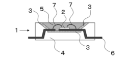
- FIG. 1 is a cross-sectional view of a schematic diagram illustrating one embodiment of a light-emitting device of the present invention.
- FIG. 2 is a top view of the schematic diagram of FIG.
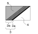
- FIG. 3 is a partially enlarged view of the schematic diagram of FIG.
- FIG. 4 is a diagram illustrating an example of an emission spectrum of the light-emitting element.
- FIG. 5 is a diagram illustrating the relationship between the number of layers of the optical multilayer film and the weighted average reflectance in the examples.
- FIG. 6 is a diagram illustrating the relationship between the ⁇ value of each layer of the 11-layer optical multilayer film and the weighted average reflectance in the example.
- FIG. 1 is a cross-sectional view of a schematic diagram illustrating one embodiment of a light-emitting device of the present invention.
- FIG. 2 is a top view of the schematic diagram of FIG.
- FIG. 3 is a partially enlarged view of the schematic diagram of FIG.
- FIG. 4 is a
- FIG. 7 is a diagram illustrating the relationship between the ⁇ value of each layer of the 21-layer optical multilayer film and the weighted average reflectance in the example.
- FIG. 8 is a diagram showing the relationship between the number of layers having an ⁇ value of 1.05 or more in the 21-layer optical multilayer film in the example and the weighted average reflectance.
- FIG. 9 is a graph showing the relationship between the number of layers having an ⁇ value other than 1.00 and the weighted average reflectance in the 21-layer optical multilayer film in the example.
- the light-emitting device of the present invention has at least a light-emitting element and a reflective film, and further has other configurations as necessary.
- Light emitting element> There is no restriction
- the material, structure, shape, and size of the light emitting diode are not particularly limited and can be appropriately selected depending on the purpose.
- a light emitting material used for the light emitting diode a material emitting light having a necessary color tone can be arbitrarily selected.
- a group III nitride compound semiconductor (Al x Ga y In 1-xy N) having a violet to green emission wavelength can be used.
- the combination of the compound semiconductor which has the light emission wavelength of a near ultraviolet to blue region, and a yellow fluorescent substance is mentioned. In this case, white light emission can be obtained.
- the structure of the light emitting diode is not particularly limited and can be appropriately selected depending on the purpose. For example, a so-called face-up type structure (light extraction to the p-type semiconductor layer side) or a so-called flip chip type structure ( Light extraction to the insulating substrate side).
- the organic EL element includes a structure having a pair of electrodes (anode and cathode) and an organic layer disposed between the pair of electrodes.
- the structure of the organic EL element includes a structure having a pair of electrodes (anode and cathode) and an organic layer disposed between the pair of electrodes.
- the structure of the organic EL element includes a structure having a pair of electrodes (anode and cathode) and an organic layer disposed between the pair of electrodes.
- stacking of the said organic layer According to the objective, it can select suitably, For example, it is laminated
- a hole injection layer may be provided between the hole transport layer and the anode. Further, a hole transporting intermediate layer may be provided between the organic light emitting layer and the hole transport layer. Further, an electron transporting intermediate layer may be provided between the organic light emitting layer and the electron transport layer. An electron injection layer may be provided between the cathode and the electron transport layer.
- the inorganic EL device There is no restriction
- the light emitting material used for the inorganic EL element include SrS: Ce, SrGa 2 S 4 , BaAl 2 S 4 : Eu, ZnS: Cu, X, ZnS: Cu, Mn, X (X is a coactivator. And any one selected from the group consisting of Cl, Br, I, and Al).
- the structure of the inorganic EL element include a structure in which a coating film containing the light emitting material is provided on a sheet of resin containing a conductor and a conductor layer is provided thereon.
- the reflective film is a reflective film in which an optical multilayer film is laminated on a metal film, and an average reflectance in a wavelength region of 400 nm to 700 nm is 90.0% or more.
- the average reflectance (hereinafter sometimes referred to as “weighted average reflectance”) can be obtained by calculation, and the calculation method is as follows.
- the incident angles of incident light on the reflective film are 6 incident angles of 0 °, 15 °, 30 °, 45 °, 60 °, and 75 ° when the direction perpendicular to the surface of the reflective film is 0 °. Use corners.
- the reflectance when light having a wavelength of 400 nm to 700 nm is incident on the reflection film from each incident angle is calculated.
- the average reflectance is calculated by obtaining an average value of these reflectances. In this case, solid angle correction is performed for each incident angle.
- light incidence from the light emitting element for example, light emitting diode
- the reflective film is not only the light that directly reaches the light emitting element.
- a light-emitting element is usually sealed with a sealant, and light from the light-emitting element undergoes total reflection at the interface between the sealant and air, and the totally reflected light reaches the reflection film.
- solid angle correction is performed in order to reflect in the calculation of the average reflectance that light incident from the light emitting element to the reflection film is random. The solid angle correction is performed by weighting the incidence frequency.
- the incident frequency is assumed to be proportional to sin ⁇ ( ⁇ is an incident angle (°) when the direction perpendicular to the surface of the reflective film is 0 °). Then, in consideration of the solid angle correction performed for each of the reflectances for the six incident angles, the average reflectance is calculated by obtaining an average value of the reflectances.
- the calculation can be performed by, for example, TFCalc (optical thin film coating property calculation software, manufactured by Software Spectra, Inc.).
- the average reflectance is preferably 91.0% or more, and more preferably 92.0% or more.
- Metal film- There is no restriction
- the thickness of the metal film is not particularly limited and may be appropriately selected depending on the intended purpose, but is preferably 10 nm to 500 nm, more preferably 20 nm to 400 nm, and particularly preferably 50 nm to 200 nm. If the thickness is less than 10 nm, the reflectivity may decrease. If the thickness exceeds 500 nm, the metal film may be peeled off from a package or the like, or the metal film may be cracked. When the thickness is within the particularly preferable range, it is advantageous in that a high reflectance can be obtained, the metal film does not peel, and the metal film does not crack.
- optical multilayer film is not particularly limited as long as it is a multilayer film in which layers having different refractive indexes are alternately stacked, and can be appropriately selected according to the purpose.
- the material having a high refractive index used for the optical multilayer film include Al 2 O 3 (aluminum oxide, refractive index 1.63), Ta 2 O 5 (tantalum oxide, refractive index 2.1), ZnO (zinc oxide). , Refractive index 2.1), CeO 2 (cerium oxide, refractive index 2.2), TiO 2 (titanium oxide, refractive index 2.39), CeF 3 (cerium fluoride, refractive index 1.63), ZnS ( Zinc sulfide, refractive index 2.3) and the like.
- Examples of the low refractive index material used for the optical multilayer film include SiO 2 (silicon oxide, refractive index 1.46), Al 2 O 3 (aluminum oxide, refractive index 1.63), LiF (lithium fluoride, Examples thereof include refractive index 1.3), CaF 2 (calcium fluoride, refractive index 1.35), and MgF 2 (magnesium fluoride, refractive index 1.39). Note that whether the refractive index is high or low is relative to the refractive index of the adjacent layer. Therefore, like the Al 2 O 3 , the high refractive index material and the low refractive index material Some materials apply to both.
- the refractive index represents the refractive index of light having a wavelength of 550 nm, which is approximately the center of the wavelength in the visible light region.
- the structure of the optical multilayer film is not particularly limited and may be appropriately selected depending on the intended purpose.
- a multilayer film in which 70 second layers are alternately stacked is preferable in that a high reflectance can be obtained.
- the difference in refractive index between the first layer and the second layer is preferably 0.1 or more, more preferably 0.2 or more, and particularly preferably 0.3 to 1.0. When the refractive index difference is less than 0.1, the reflectance of the reflective film may be lowered. When the refractive index difference is within the particularly preferable range, it is advantageous in that a reflective film having a high reflectance can be obtained.
- the structure of the optical multilayer film is preferably a multilayer film in which titanium oxide layers and silicon oxide layers are alternately laminated from the viewpoint of refractive index and storage stability.
- the number of layers of the optical multilayer film is not particularly limited and may be appropriately selected according to the purpose.
- the lower limit is preferably 5 layers or more, more preferably 7 layers or more, and particularly 11 layers or more. preferable.
- As an upper limit 300 layers or less are preferable, 200 layers or less are more preferable, and 100 layers or less are especially preferable.
- the reflectance of the reflective film may be lowered.
- the number of layers is within the particularly preferable range, it is advantageous in that a reflective film having a high reflectance can be obtained and the durability of the reflective film is excellent.
- required by following formula (1) is 1.05 or more. Having a layer is preferable in that a reflective film having a high reflectance can be obtained.
- the ⁇ is more preferably 1.15 or more, and particularly preferably 1.25 or more.
- ⁇ 4 ⁇ n ⁇ d / ⁇ Equation (1)
- d (nm) represents the thickness of the layer
- n represents the refractive index of the layer
- ⁇ (nm) represents ( ⁇ 1 + ⁇ 2 ) / 2.
- ⁇ 1 is the shortest wavelength among the wavelengths that are 1/10 of the light intensity of the peak wavelength in the emission wavelength of the light emitting element in the wavelength region of 200 nm to 1,000 nm
- ⁇ 2 is the wavelength of 200 nm to 1,000 nm.
- the emission wavelength of the light emitting element in the region indicates the longest wavelength among the wavelengths that are 1/10 of the light intensity of the peak wavelength.
- the optical multilayer film preferably has two or more layers that satisfy ⁇ required by the formula (1), and more preferably has three or more layers. It is more preferable to have 5 layers or more, and it is particularly preferable to have 7 layers or more.
- d ⁇ / (4 ⁇ n) is generally known as an equation indicating the optimum layer thickness (d) for increasing the reflectance of light having a wavelength of ⁇ nm.
- the optical multilayer film has a thickness of 1.05 than that of the layer in which ⁇ obtained by the equation (1) is 1. It is presumed that the above layer is more advantageous for angle dependency.
- ⁇ ( ⁇ 1 + ⁇ 2 ) / 2
- ⁇ 1 is 1/10 of the light intensity at the peak wavelength in the emission wavelength of the light emitting element in the wavelength region of 200 nm to 1,000 nm.
- ⁇ 2 indicates the longest wavelength among the wavelengths that are 1/10 of the light intensity of the peak wavelength in the light emission wavelength of the light emitting element in the wavelength region of 200 nm to 1,000 nm. It is said.
- the emission spectrum from the light emitting element usually has a peak in the visible light region and is broad in the visible light region, not a single wavelength.
- ⁇ 1 , ⁇ 2 , and ⁇ ( ⁇ 1 + ⁇ 2 ) / 2 are defined in order to obtain the center wavelength of such a broad emission spectrum.
- the method for forming each layer of the optical multilayer film is not particularly limited and may be appropriately selected depending on the intended purpose.
- Examples thereof include a vacuum deposition method, a sputtering method, a plasma CVD method, and a sol-gel method.
- Examples of the vacuum deposition method include a reactive deposition method, an ion beam assisted deposition method, and an ion plating method.
- Examples of the sputtering method include a DC / RF sputtering method and a reactive sputtering method.
- the sol-gel method include a polymerization method and a colloid method.
- the vacuum vapor deposition method and the sputtering method are preferable because a uniform and thin layer can be formed, and the reactive vapor deposition method, the ion beam assisted vapor deposition method, the ion plating method, and the reactive sputtering method are more preferable.
- the reflection film for example, as a reflection film having five optical multilayer films, when a high refractive index layer is H and a low refractive index layer is L, a metal film / H / L / H / L
- stacked in order of / H is mentioned. Specific examples include a reflective film in which metal film / titanium oxide layer / silicon oxide layer / titanium oxide layer / silicon oxide layer / titanium oxide layer are stacked in this order.
- the package is not particularly limited as long as it has a role as a table on which the light-emitting element is mounted or a support for the reflective film, and there are no particular restrictions on the package, and the package is appropriately selected according to the purpose. You can choose.
- the material of the package include ceramic and resin. There is no restriction
- the shape of the package include a shape having a tapered recess. In the package having the tapered recess, the light emitting element is disposed, for example, at the bottom of the recess, and the reflective film is disposed, for example, at least one of the bottom and the side of the recess. Yes.
- the sealing portion is used for suppressing deterioration of the performance of the light emitting element due to oxygen or moisture in the atmosphere.
- a material of the said sealing part there is no restriction
- an epoxy resin is preferable from the viewpoint of the function of preventing moisture from entering.
- thermosetting epoxy resins and photocurable epoxy resins are more preferable.
- the method for forming the sealing part is not particularly limited and may be appropriately selected depending on the intended purpose. Examples thereof include a method of applying a resin solution and a method of pressure bonding or thermocompression bonding of a resin sheet.
- the material, structure, shape and size thereof are not particularly limited and can be appropriately selected according to the purpose.
- the material of the lead frame include iron, copper, iron-containing copper, tin-containing copper, and the like.
- the shape of the lead frame include a plate shape and a rod shape.
- the bonding wire is not particularly limited as long as it enables electrical connection between the lead frame and the electrode of the light emitting element, and the bonding wire is not particularly limited. It can be selected appropriately. Examples of the material of the bonding wire include gold, copper, platinum, aluminum, and alloys thereof.
- FIG. 1 is a schematic cross-sectional view showing an embodiment of the light-emitting device.
- FIG. 2 is a top view of the schematic view of the light emitting device of FIG.
- FIG. 3 is a partially enlarged view of the cross-sectional view of FIG.
- the light emitting device 1 includes a light emitting element 2, a reflective film 3, a package 4, a sealing portion 5, a lead frame 6, and a bonding wire 7.
- the lead frame 6 is embedded in the package 4.
- the package 4 has a tapered recess.
- the light emitting element 2 is bonded to the lead frame 6 with a bonding material and placed on the bottom of the recess.
- the reflective film 3 is formed on the bottom and side portions of the recess. As shown in FIG. 3, the reflective film 3 has a structure in which a metal film 3a and then an optical multilayer film 3b are sequentially formed from the package 4 side.
- the optical multilayer film 3b has a structure in which layers having a high refractive index and layers having a low refractive index are alternately stacked in order from the metal film 3a side.
- the optical multilayer film 3b has a five-layer structure.
- the light emitting element 2 and the lead frame 6 are electrically connected by the bonding wire 7.
- the sealing part 5 is formed in the taper-shaped recessed part of the said package 4 so that the recessed part may be filled up.
- Example 1 The weighted average reflectance of the reflective film of the light emitting device was calculated using calculation software.
- ⁇ Structure of reflective film> The reflective film to be calculated uses aluminum as a metal film, and on the aluminum, a layer of titanium oxide (TiO 2 ) / a layer of silicon oxide (SiO 2 ) / a layer of titanium oxide (TiO 2 ) / silicon oxide It was constructed using the (SiO 2) layer / titanium oxide order five layers laminated optical multilayer film of layers of (TiO 2).
- the thickness of aluminum was 100 nm.
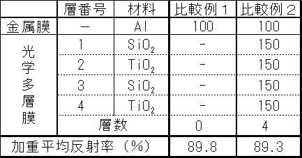
- the thickness of the titanium oxide layer and the thickness of the silicon oxide layer in the optical multilayer film were as shown in Table 1-1.
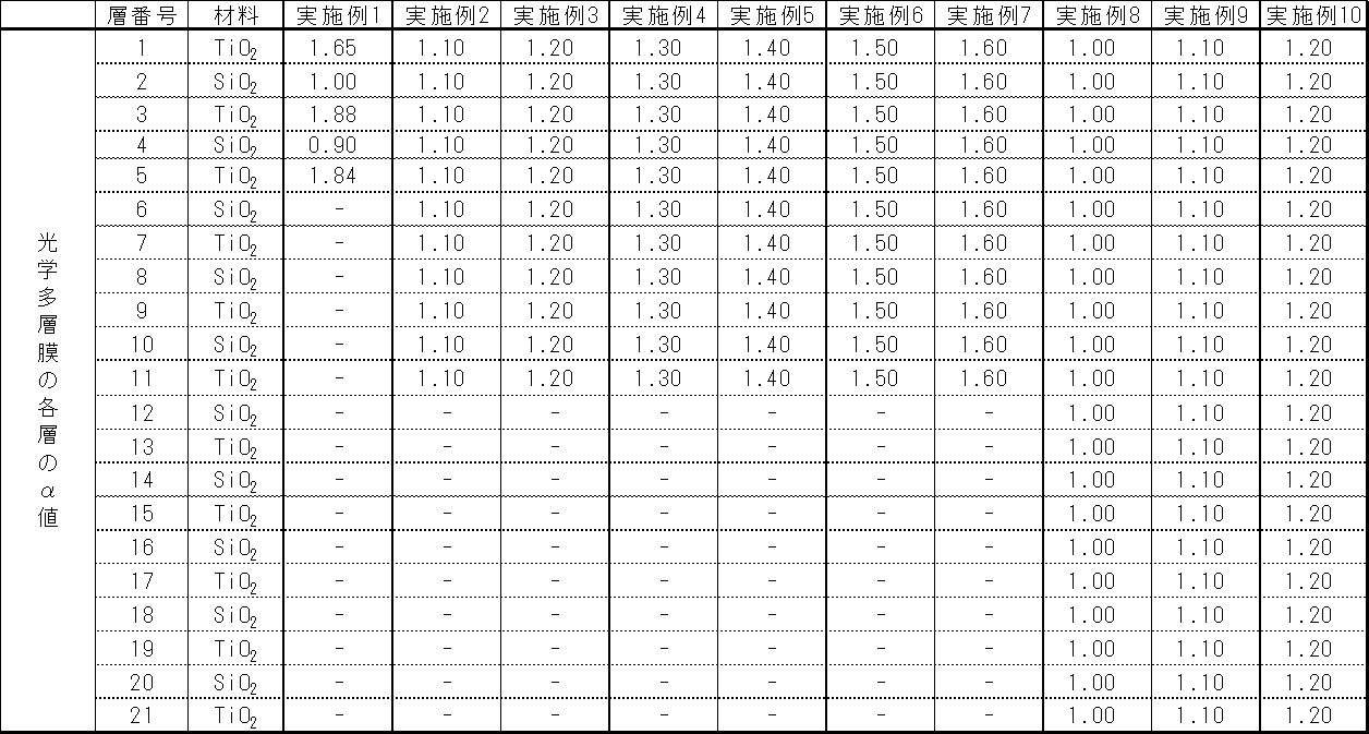
- ⁇ in the formula (1) of each layer is as shown in Table 2-1.
- the refractive index of the titanium oxide layer was 2.39, and the refractive index of the silicon oxide layer was 1.46.
- the weighted average reflectance of the reflective film was calculated using TFCalc (Optical thin film coating property calculation software, manufactured by Software Spectra, Inc.).
- the incident angles of incident light on the reflective film are 6 incident angles of 0 °, 15 °, 30 °, 45 °, 60 °, and 75 ° when the direction perpendicular to the surface of the reflective film is 0 °. Corners were used.
- the reflectance when light having a wavelength of 400 nm to 700 nm was incident on the reflective film from each incident angle was calculated.
- the said weighted average reflectance was calculated by calculating
- the solid angle correction was performed by weighting the incidence frequency.
- the incident frequency is proportional to sin ⁇ ( ⁇ is an incident angle (°) when the direction perpendicular to the surface of the reflective film is 0 °).
- the weighted average reflectance was calculated by calculating an average value of the reflectances after taking into account the solid angle correction performed for each of the reflectances with respect to the six incident angles. The calculation result of the weighted average reflectance is shown in Table 1-1.
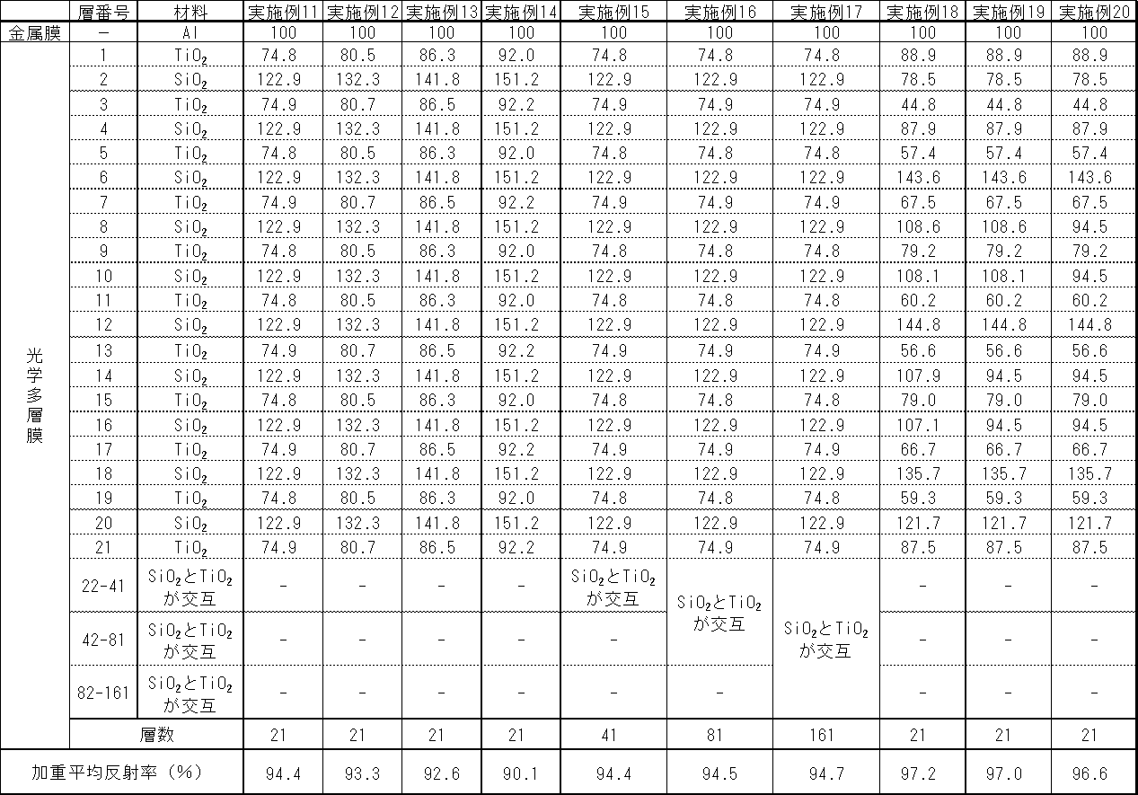
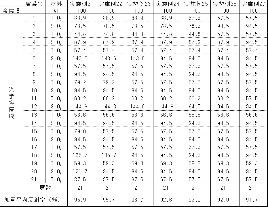
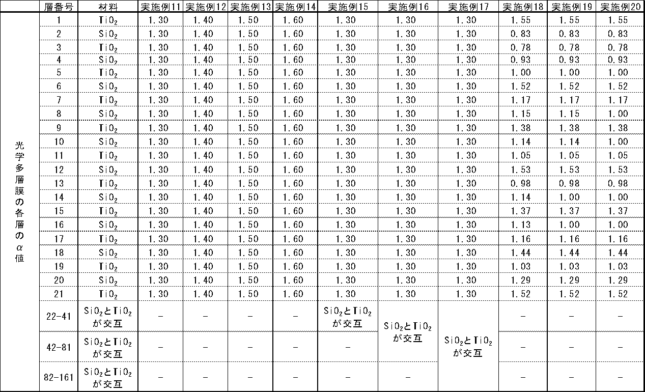
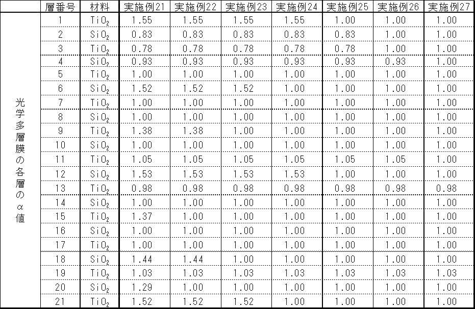
- Example 2 to 27 and Comparative Examples 1 and 2 In Example 1, except that the optical multilayer film was replaced with the optical multilayer film having the number of layers, the thickness of each layer, and the material of each layer shown in Table 1-1 to Table 1-4, in the same manner as in Example 1, The weighted average reflectances of Examples 2 to 27 and Comparative Examples 1 and 2 were calculated. The calculation results are shown in Table 1-1 to Table 1-4. ⁇ in the formula (1) of Examples 2 to 27 and Comparative Examples 1 and 2 is as shown in Tables 2-1 to 2-4. In Example 15, the layer numbers 22 to 41 are alternately composed of a 122.9 nm thick silicon oxide layer ( ⁇ is 1.30) and a 74.9 nm thick titanium oxide layer ( ⁇ is 1.30). Are stacked.
- the layer number 22 is a silicon oxide layer, and the layer number 41 is a titanium oxide layer.
- layer numbers 22 to 81 are formed by alternately stacking 122.9 nm thick silicon oxide layers ( ⁇ is 1.30) and 74.9 nm thick titanium oxide layers ( ⁇ is 1.30). ing.
- the layer number 22 is a silicon oxide layer, and the layer number 81 is a titanium oxide layer.
- layer numbers 22 to 161 are formed by alternately laminating 122.9 nm thick silicon oxide layers ( ⁇ is 1.30) and 74.9 nm thick titanium oxide layers ( ⁇ is 1.30). ing.
- the layer number 22 is a silicon oxide layer, and the layer number 161 is a titanium oxide layer.
- Table 1-1 to Table 1-4 the numerical values in each column excluding the column of the number of layers and the weighted average reflectance indicate the thickness (nm).
- Tables 1-1 to 1-4 and Tables 2-1 to 2-4 the smaller the layer number, the closer to the metal film (aluminum).
- the titanium oxide layer of layer number 1 is a layer in contact with aluminum.
- the reflective film of the light emitting device of the present invention had an excellent weighted average reflectance of 90.0% or more.
- the 11-layer has a considerably excellent weighted average reflectance of 91.3%, and the weighted average reflectance becomes higher as the number of layers increases. It had an excellent weighted average reflectance.
- the weighted average reflectance increases as the number of layers having an ⁇ value of 1.05 or more increases.
- the light emitting device of the present invention has high reflectance, it can be suitably used as a light source for illumination and display.
Landscapes
- Physics & Mathematics (AREA)
- Optics & Photonics (AREA)
- Led Device Packages (AREA)
Abstract
発光素子と反射膜とを有する発光装置であって、前記反射膜が、金属膜上に光学多層膜を積層した反射膜であり、かつ400nm~700nmの波長領域における平均反射率が90.0%以上である発光装置である。
Description
本発明は、照明、表示のための光源などに適用可能な発光装置に関する。
発光ダイオードや有機EL素子などを備えた発光装置は、白色の発光色を得ることができ、小型であり、低電圧で駆動することができ、更に長寿命であるという利点を有することから、照明や表示のための光源への検討が盛んに行われている。
発光ダイオードは、通常、0.3mm~1mm角の微小なチップであることから、機械的強度を保ち、取扱いを容易にし、大気中の酸素や水分による発光素子性能の劣化を抑制するために、封止剤により封止されている。また、有機EL素子も、通常、同様の目的から封止剤により封止されている。しかしながら、封止剤により封止した場合、封止剤により光の取出しが阻害され、光の取出し効率が低くなるという問題がある。
このようなこともあり、発光装置には、光の取出し効率を高めることが要求されている。
光の取出し効率を高めるためには、高い反射率を有する反射膜を発光装置に備えることが有効である。そこで、白色の反射膜を備えた発光装置や、金属からなる反射膜を備えた発光装置(特許文献1参照)が提案されている。
しかしながら、これら提案の技術は、反射膜の反射率が要求される程度にまでは至っていないという問題がある。
光の取出し効率を高めるためには、高い反射率を有する反射膜を発光装置に備えることが有効である。そこで、白色の反射膜を備えた発光装置や、金属からなる反射膜を備えた発光装置(特許文献1参照)が提案されている。
しかしながら、これら提案の技術は、反射膜の反射率が要求される程度にまでは至っていないという問題がある。
また、実装基板の表面に金属膜と光学多層膜とを積層した反射膜を有する発光装置が提案されている(特許文献2参照)。この提案の技術では、SiO2膜とTiO2膜を交互に積層した4層構造の光学多層膜が使用されている。
この提案の技術は、白色の反射膜を備えた発光装置や金属からなる反射膜を備えた発光3装置よりは反射率が優れるものの、反射膜の反射率は要求される程度にまでは至っていないという問題がある。
この提案の技術は、白色の反射膜を備えた発光装置や金属からなる反射膜を備えた発光3装置よりは反射率が優れるものの、反射膜の反射率は要求される程度にまでは至っていないという問題がある。
したがって、反射率が高い発光装置の提供が求められているのが現状である。
本発明は、従来における前記諸問題を解決し、以下の目的を達成することを課題とする。即ち、本発明は、反射率が高い発光装置を提供することを目的とする。
前記課題を解決するための手段としては、以下の通りである。即ち、
<1> 発光素子と反射膜とを有する発光装置であって、
前記反射膜が、金属膜上に光学多層膜を積層した反射膜であり、かつ400nm~700nmの波長領域における平均反射率が90.0%以上であることを特徴とする発光装置である。
<2> 光学多層膜の層数が、5層以上である前記<1>に記載の発光装置である。
<3> 光学多層膜が、下記式(1)で求められるαが1.05以上である層を有する前記<1>から<2>のいずれかに記載の発光装置である。
α=4×n×d/λ 式(1)
ここで、d(nm)は層の厚み、nは層の屈折率、λ(nm)は(λ1+λ2)/2を示す。λ1は200nm~1,000nmの波長領域における発光素子の発光波長において、ピーク波長の光強度の1/10となる波長のうちの最も短い波長を示し、λ2は200nm~1,000nmの波長領域における発光素子の発光波長において、ピーク波長の光強度の1/10となる波長のうちの最も長い波長を示す。
<4> 光学多層膜が、式(1)で求められるαが1.05以上である層を2層以上有する前記<3>に記載の発光装置である。
<5> 光学多層膜が、屈折率1.60~2.80の第一の層と、屈折率1.20~1.70の第二の層とが交互に積層した多層膜であり、前記第一の層と前記第二の層との屈折率差が0.1以上である前記<1>から<4>のいずれかに記載の発光装置である。
<6> 光学多層膜が、酸化チタンの層と酸化ケイ素の層とが交互に積層した多層膜である前記<1>から<5>のいずれかに記載の発光装置である。
<7> 発光素子が、発光ダイオードである前記<1>から<6>のいずれかに記載の発光装置である。
<1> 発光素子と反射膜とを有する発光装置であって、
前記反射膜が、金属膜上に光学多層膜を積層した反射膜であり、かつ400nm~700nmの波長領域における平均反射率が90.0%以上であることを特徴とする発光装置である。
<2> 光学多層膜の層数が、5層以上である前記<1>に記載の発光装置である。
<3> 光学多層膜が、下記式(1)で求められるαが1.05以上である層を有する前記<1>から<2>のいずれかに記載の発光装置である。
α=4×n×d/λ 式(1)
ここで、d(nm)は層の厚み、nは層の屈折率、λ(nm)は(λ1+λ2)/2を示す。λ1は200nm~1,000nmの波長領域における発光素子の発光波長において、ピーク波長の光強度の1/10となる波長のうちの最も短い波長を示し、λ2は200nm~1,000nmの波長領域における発光素子の発光波長において、ピーク波長の光強度の1/10となる波長のうちの最も長い波長を示す。
<4> 光学多層膜が、式(1)で求められるαが1.05以上である層を2層以上有する前記<3>に記載の発光装置である。
<5> 光学多層膜が、屈折率1.60~2.80の第一の層と、屈折率1.20~1.70の第二の層とが交互に積層した多層膜であり、前記第一の層と前記第二の層との屈折率差が0.1以上である前記<1>から<4>のいずれかに記載の発光装置である。
<6> 光学多層膜が、酸化チタンの層と酸化ケイ素の層とが交互に積層した多層膜である前記<1>から<5>のいずれかに記載の発光装置である。
<7> 発光素子が、発光ダイオードである前記<1>から<6>のいずれかに記載の発光装置である。
本発明によると、従来における前記諸問題を解決することができ、反射率が高い発光装置を提供することができる。
(発光装置)
本発明の発光装置は、発光素子と反射膜とを少なくとも有し、更に必要に応じて、その他の構成を有する。
本発明の発光装置は、発光素子と反射膜とを少なくとも有し、更に必要に応じて、その他の構成を有する。
<発光素子>
前記発光素子としては、特に制限はなく、目的に応じて適宜選択することができ、例えば、発光ダイオード、有機EL素子、無機EL素子などが挙げられる。これらの中でも、発光ダイオードが、光量が多い点、高い反射率が得られる点で好ましい。
前記発光素子としては、特に制限はなく、目的に応じて適宜選択することができ、例えば、発光ダイオード、有機EL素子、無機EL素子などが挙げられる。これらの中でも、発光ダイオードが、光量が多い点、高い反射率が得られる点で好ましい。
-発光ダイオード-
前記発光ダイオードの材料、構造、形状、大きさとしては、特に制限はなく、目的に応じて適宜選択することができる。
前記発光ダイオードに用いられる発光材料としては、必要な色調を発光するものを任意に選択できる。例えば、紫色から緑色の発光波長を有するIII族窒化物系化合物半導体(AlxGayIn1-x-yN)などが挙げられる。また、近紫外から青色領域の発光波長を有する化合物半導体と、黄色蛍光体との組合せが挙げられる。この場合は、白色発光を得ることができる。
前記発光ダイオードの構造としては、特に制限はなく、目的に応じて適宜選択することができ、例えば、いわゆるフェイスアップタイプの構造(p型半導体層側に光取出し)やいわゆるフリップチップタイプの構造(絶縁基板側に光取出し)などが挙げられる。
前記発光ダイオードの材料、構造、形状、大きさとしては、特に制限はなく、目的に応じて適宜選択することができる。
前記発光ダイオードに用いられる発光材料としては、必要な色調を発光するものを任意に選択できる。例えば、紫色から緑色の発光波長を有するIII族窒化物系化合物半導体(AlxGayIn1-x-yN)などが挙げられる。また、近紫外から青色領域の発光波長を有する化合物半導体と、黄色蛍光体との組合せが挙げられる。この場合は、白色発光を得ることができる。
前記発光ダイオードの構造としては、特に制限はなく、目的に応じて適宜選択することができ、例えば、いわゆるフェイスアップタイプの構造(p型半導体層側に光取出し)やいわゆるフリップチップタイプの構造(絶縁基板側に光取出し)などが挙げられる。
-有機EL素子-
前記有機EL素子の材料、構造、形状、大きさとしては、特に制限はなく、目的に応じて適宜選択することができる。
前記有機EL素子の構造としては、例えば、一対の電極(陽極及び陰極)と、前記一対の電極間に配置された有機層とを有する構造などが挙げられる。
前記有機層の積層の形態としては、特に制限はなく、目的に応じて適宜選択することができ、例えば、陽極側から、正孔輸送層、有機発光層、電子輸送層の順に積層されている形態などが挙げられる。この形態において、正孔輸送層と陽極との間には正孔注入層が設けられていてもよい。また、有機発光層と正孔輸送層との間には正孔輸送性中間層が設けられていてもよい。また、有機発光層と電子輸送層との間には電子輸送性中間層が設けられていてもよい。また、陰極と電子輸送層との間には電子注入層が設けられていてもよい。
前記有機EL素子の材料、構造、形状、大きさとしては、特に制限はなく、目的に応じて適宜選択することができる。
前記有機EL素子の構造としては、例えば、一対の電極(陽極及び陰極)と、前記一対の電極間に配置された有機層とを有する構造などが挙げられる。
前記有機層の積層の形態としては、特に制限はなく、目的に応じて適宜選択することができ、例えば、陽極側から、正孔輸送層、有機発光層、電子輸送層の順に積層されている形態などが挙げられる。この形態において、正孔輸送層と陽極との間には正孔注入層が設けられていてもよい。また、有機発光層と正孔輸送層との間には正孔輸送性中間層が設けられていてもよい。また、有機発光層と電子輸送層との間には電子輸送性中間層が設けられていてもよい。また、陰極と電子輸送層との間には電子注入層が設けられていてもよい。
-無機EL素子-
前記無機EL素子の材料、構造、形状、大きさとしては、特に制限はなく、目的に応じて適宜選択することができる。
前記無機EL素子に用いられる発光材料としては、例えば、SrS:Ce、SrGa2S4、BaAl2S4:Eu、ZnS:Cu,X、ZnS:Cu,Mn,X(Xは共賦活剤であり、Cl、Br、I、Alの群の中から選ばれるいずれかである。)などが挙げられる。
前記無機EL素子の構造としては、例えば、導電体を含む樹脂などのシートの上に前記発光材料を含む塗膜を設け、その上に導電体層を設けた構造などが挙げられる。
前記無機EL素子の材料、構造、形状、大きさとしては、特に制限はなく、目的に応じて適宜選択することができる。
前記無機EL素子に用いられる発光材料としては、例えば、SrS:Ce、SrGa2S4、BaAl2S4:Eu、ZnS:Cu,X、ZnS:Cu,Mn,X(Xは共賦活剤であり、Cl、Br、I、Alの群の中から選ばれるいずれかである。)などが挙げられる。
前記無機EL素子の構造としては、例えば、導電体を含む樹脂などのシートの上に前記発光材料を含む塗膜を設け、その上に導電体層を設けた構造などが挙げられる。
<反射膜>
前記反射膜は、金属膜上に光学多層膜を積層した反射膜であり、かつ400nm~700nmの波長領域における平均反射率が90.0%以上である。
前記反射膜は、金属膜上に光学多層膜を積層した反射膜であり、かつ400nm~700nmの波長領域における平均反射率が90.0%以上である。
-平均反射率-
前記平均反射率(以下、「加重平均反射率」と称することがある。)は計算により求めることができ、その計算方法は以下の通りである。
前記反射膜への入射光の入射角は、前記反射膜の面に対して垂直方向を0°とした際の0°、15°、30°、45°、60°、75°の6つの入射角を用いる。そして、前記反射膜に対して、それぞれの入射角から波長400nm~700nmの光を入射させた際の反射率を計算する。そして、それら反射率の平均値を求めることにより前記平均反射率を計算するが、その際には、入射角毎に立体角補正を行う。
発光素子(例えば発光ダイオード)から反射膜への光入射は、ランダムであると仮定できる。なぜなら、反射膜へ入ってくる光は、発光素子から直接届く光だけではない。例えば、発光素子は通常封止剤で封止されており、発光素子からの光は封止剤と空気との界面で全反射をおこし、その全反射した光が反射膜に届く。このように、反射膜へ入ってくる光には様々な光があるため、反射膜へはランダムな方向から光が入射する。そこで、発光素子から反射膜への光入射がランダムであることを前記平均反射率の算出に反映させるために、立体角補正を行っている。前記立体角補正は、入射頻度の重み付けにより行っている。入射頻度はsinα(αは、反射膜の面に対して垂直方向を0°とした際の入射角(°))に比例するものとしている。
そして、前記6つの入射角に対する反射率それぞれについて行った立体角補正を考慮した上で、それら反射率の平均値を求めることにより前記平均反射率が計算される。
前記計算は、例えば、TFcalc(光学薄膜コーティング特性計算ソフト、Software Spectra,Inc.製)により行うことができる。
前記平均反射率(以下、「加重平均反射率」と称することがある。)は計算により求めることができ、その計算方法は以下の通りである。
前記反射膜への入射光の入射角は、前記反射膜の面に対して垂直方向を0°とした際の0°、15°、30°、45°、60°、75°の6つの入射角を用いる。そして、前記反射膜に対して、それぞれの入射角から波長400nm~700nmの光を入射させた際の反射率を計算する。そして、それら反射率の平均値を求めることにより前記平均反射率を計算するが、その際には、入射角毎に立体角補正を行う。
発光素子(例えば発光ダイオード)から反射膜への光入射は、ランダムであると仮定できる。なぜなら、反射膜へ入ってくる光は、発光素子から直接届く光だけではない。例えば、発光素子は通常封止剤で封止されており、発光素子からの光は封止剤と空気との界面で全反射をおこし、その全反射した光が反射膜に届く。このように、反射膜へ入ってくる光には様々な光があるため、反射膜へはランダムな方向から光が入射する。そこで、発光素子から反射膜への光入射がランダムであることを前記平均反射率の算出に反映させるために、立体角補正を行っている。前記立体角補正は、入射頻度の重み付けにより行っている。入射頻度はsinα(αは、反射膜の面に対して垂直方向を0°とした際の入射角(°))に比例するものとしている。
そして、前記6つの入射角に対する反射率それぞれについて行った立体角補正を考慮した上で、それら反射率の平均値を求めることにより前記平均反射率が計算される。
前記計算は、例えば、TFcalc(光学薄膜コーティング特性計算ソフト、Software Spectra,Inc.製)により行うことができる。
前記平均反射率は、91.0%以上が好ましく、92.0%以上がより好ましい。
-金属膜-
前記金属膜の材質としては、特に制限はなく、目的に応じて適宜選択することができ、例えば、金、銀、アルミニウムなどが挙げられる。これらの中でも、反射膜の反射率が優れる点、並びに熱及び湿気に対する安定性の点からアルミニウムが好ましい。
前記金属膜の材質としては、特に制限はなく、目的に応じて適宜選択することができ、例えば、金、銀、アルミニウムなどが挙げられる。これらの中でも、反射膜の反射率が優れる点、並びに熱及び湿気に対する安定性の点からアルミニウムが好ましい。
前記金属膜の厚みとしては、特に制限はなく、目的に応じて適宜選択することができるが、10nm~500nmが好ましく、20nm~400nmがより好ましく、50nm~200nmが特に好ましい。前記厚みが、10nm未満であると、反射率が低下することがあり、500nmを超えると、前記金属膜がパッケージなどから剥離したり、前記金属膜にひびが入ることがある。前記厚みが、前記特に好ましい範囲であると、高い反射率が得られる点、前記金属膜が剥離しない点、及び前記金属膜にひびが入ることがない点で有利である。
前記金属膜の形成方法としては、特に制限はなく、目的に応じて適宜選択することができ、例えば、真空蒸着法、スパッタリング法、プラズマCVD法、無電解メッキ法、電解メッキ法などが挙げられる。
-光学多層膜-
前記光学多層膜としては、屈折率の異なる層が交互に積層された多層膜であれば、特に制限はなく、目的に応じて適宜選択することができる。
前記光学多層膜としては、屈折率の異なる層が交互に積層された多層膜であれば、特に制限はなく、目的に応じて適宜選択することができる。
前記光学多層膜の材料としては、特に制限はなく、目的に応じて適宜選択することができる。
前記光学多層膜に用いる屈折率の高い材料としては、例えば、Al2O3(酸化アルミニウム、屈折率1.63)、Ta2O5(酸化タンタル、屈折率2.1)、ZnO(酸化亜鉛、屈折率2.1)、CeO2(酸化セリウム、屈折率2.2)、TiO2(酸化チタン、屈折率2.39)、CeF3(フッ化セリウム、屈折率1.63)、ZnS(硫化亜鉛、屈折率2.3)などが挙げられる。
前記光学多層膜に用いる屈折率の低い材料としては、例えば、SiO2(酸化ケイ素、屈折率1.46)、Al2O3(酸化アルミニウム、屈折率1.63)、LiF(フッ化リチウム、屈折率1.3)、CaF2(フッ化カルシウム、屈折率1.35)、MgF2(フッ化マグネシウム、屈折率1.39)などが挙げられる。
なお、屈折率が高いか低いかは、隣接する層の屈折率に対する相対的なものであるため、前記Al2O3のように、前記屈折率の高い材料、及び前記屈折率の低い材料のいずれにも当てはまる材料もある。
前記光学多層膜に用いる屈折率の高い材料としては、例えば、Al2O3(酸化アルミニウム、屈折率1.63)、Ta2O5(酸化タンタル、屈折率2.1)、ZnO(酸化亜鉛、屈折率2.1)、CeO2(酸化セリウム、屈折率2.2)、TiO2(酸化チタン、屈折率2.39)、CeF3(フッ化セリウム、屈折率1.63)、ZnS(硫化亜鉛、屈折率2.3)などが挙げられる。
前記光学多層膜に用いる屈折率の低い材料としては、例えば、SiO2(酸化ケイ素、屈折率1.46)、Al2O3(酸化アルミニウム、屈折率1.63)、LiF(フッ化リチウム、屈折率1.3)、CaF2(フッ化カルシウム、屈折率1.35)、MgF2(フッ化マグネシウム、屈折率1.39)などが挙げられる。
なお、屈折率が高いか低いかは、隣接する層の屈折率に対する相対的なものであるため、前記Al2O3のように、前記屈折率の高い材料、及び前記屈折率の低い材料のいずれにも当てはまる材料もある。
ここで、本発明において屈折率とは、可視光領域の波長の概ね中心である波長550nmの光における屈折率を表す。
前記光学多層膜の構造としては、特に制限はなく、目的に応じて適宜選択することができるが、屈折率1.60~2.80の第一の層と、屈折率1.20~1.70の第二の層とが交互に積層した多層膜であることが、高い反射率が得られる点で好ましい。
そして、前記第一の層と前記第二の層との屈折率差は、0.1以上が好ましく、0.2以上がより好ましく、0.3~1.0が特に好ましい。前記屈折率差が、0.1未満であると、反射膜の反射率が低くなることがある。前記屈折率差が、前記特に好ましい範囲であると、高い反射率の反射膜が得られる点で有利である。
そして、前記第一の層と前記第二の層との屈折率差は、0.1以上が好ましく、0.2以上がより好ましく、0.3~1.0が特に好ましい。前記屈折率差が、0.1未満であると、反射膜の反射率が低くなることがある。前記屈折率差が、前記特に好ましい範囲であると、高い反射率の反射膜が得られる点で有利である。
また、前記光学多層膜の構造としては、酸化チタンの層と酸化ケイ素の層とが交互に積層した多層膜であることが、屈折率の点、及び保存安定性の点から好ましい。
前記光学多層膜の層数としては、特に制限はなく、目的に応じて適宜選択することができるが、下限値としては、5層以上が好ましく、7層以上がより好ましく、11層以上が特に好ましい。上限値としては、300層以下が好ましく、200層以下がより好ましく、100層以下が特に好ましい。前記層数が、5層未満であると、反射膜の反射率が低くなることがある。前記層数が、前記特に好ましい範囲であると、高い反射率の反射膜が得られる点、及び反射膜の耐久性が優れる点で有利である。
前記光学多層膜の各層の厚みとしては、特に制限はなく、目的に応じて適宜選択することができるが、前記光学多層膜が、下記式(1)で求められるαが1.05以上である層を有することが、高い反射率の反射膜が得られる点で好ましい。また、前記αが、1.15以上であることがより好ましく、1.25以上であることが特に好ましい。また、上限値としては、1.60以下であることが好ましく、1.50以下であることがより好ましい。
α=4×n×d/λ 式(1)
ここで、d(nm)は層の厚み、nは層の屈折率、λ(nm)は(λ1+λ2)/2を示す。λ1は200nm~1,000nmの波長領域における発光素子の発光波長において、ピーク波長の光強度の1/10となる波長のうちの最も短い波長を示し、λ2は200nm~1,000nmの波長領域における発光素子の発光波長において、ピーク波長の光強度の1/10となる波長のうちの最も長い波長を示す。
α=4×n×d/λ 式(1)
ここで、d(nm)は層の厚み、nは層の屈折率、λ(nm)は(λ1+λ2)/2を示す。λ1は200nm~1,000nmの波長領域における発光素子の発光波長において、ピーク波長の光強度の1/10となる波長のうちの最も短い波長を示し、λ2は200nm~1,000nmの波長領域における発光素子の発光波長において、ピーク波長の光強度の1/10となる波長のうちの最も長い波長を示す。
また、高い反射率の反射膜が得られる点から、前記光学多層膜が、前記式(1)で求められるαを満たす層を、2層以上有することが好ましく、3層以上有することがより好ましく、5層以上有することが更に好ましく、7層以上有することが特に好ましい。
前記式(1)において、α=1の場合、前記式(1)を変形するとd=λ/(4×n)となる。d=λ/(4×n)は、一般に、波長λnmの光の反射率を高くするための最適な層の厚み(d)を示す式として知られているものである。
ここで、前記発光装置のように、前記反射膜への光入射がランダムな場合には、前記光学多層膜において、前記式(1)で求められるαが1である層よりも、1.05以上である層の方が角度依存性に有利であると推測される。
前記式(1)においては、λ=(λ1+λ2)/2とし、λ1は200nm~1,000nmの波長領域における発光素子の発光波長において、ピーク波長の光強度の1/10となる波長のうちの最も短い波長を示し、λ2は200nm~1,000nmの波長領域における発光素子の発光波長において、ピーク波長の光強度の1/10となる波長のうちの最も長い波長を示すものとしている。発光素子からの発光スペクトルは、通常、単一の波長ではなく、可視光領域にピークを持ち、可視光領域にブロードなものである。そのため、そのようなブロードな発光スペクトルを持つ発光素子からの光に対して、反射特性のよい反射膜を得ることができる光学多層膜中の層の厚み(d)を算出するためには、ブロードな発光スペクトルの中心の波長を求めることを要する。そこで、λ1、λ2、及びλ=(λ1+λ2)/2は、そのようなブロードな発光スペクトルの中心の波長を求めるために規定したものである。
前記光学多層膜の各層の形成方法としては、特に制限はなく、目的に応じて適宜選択することができ、例えば、真空蒸着法、スパッタリング法、プラズマCVD法、ゾル-ゲル法などが挙げられる。前記真空蒸着法としては、例えば、反応性蒸着法、イオンビームアシスト蒸着法、イオンプレーティング法などが挙げられる。前記スパッタリング法としては、例えば、DC/RFスパッタリング法、反応性スパッタリング法などが挙げられる。前記ゾル-ゲル法としては、例えば、重合法、コロイド法などが挙げられる。これらの中でも、均一で薄い層が形成可能な点から、真空蒸着法、スパッタリング法が好ましく、反応性蒸着法、イオンビームアシスト蒸着法、イオンプレーティング法、反応性スパッタリング法がより好ましい。
前記反射膜において、例えば、5層の光学多層膜を有する反射膜としては、屈折率の高い層をHとし、屈折率の低い層をLとした場合、金属膜/H/L/H/L/Hの順に積層された反射膜が挙げられる。具体的には、金属膜/酸化チタンの層/酸化ケイ素の層/酸化チタンの層/酸化ケイ素の層/酸化チタンの層の順に積層された反射膜などが挙げられる。
<その他の構成>
前記その他の構成としては、パッケージ、封止部、リードフレーム、ボンディングワイヤーなどが挙げられる。
前記その他の構成としては、パッケージ、封止部、リードフレーム、ボンディングワイヤーなどが挙げられる。
-パッケージ-
前記パッケージは、前記発光素子を載置する台や前記反射膜の支持体としての役割を有するものであれば、その材料、構造、形状、大きさは、特に制限はなく、目的に応じて適宜選択することができる。
前記パッケージの材料としては、例えば、セラミック、樹脂などが挙げられる。前記樹脂としては、特に制限はなく、目的に応じて適宜選択することができ、例えば、アクリル系樹脂、エポキシ系樹脂、フッ素系樹脂、シリコン系樹脂、ゴム系樹脂、エステル系樹脂などが挙げられる。
前記パッケージの形状としては、例えば、テーパー形状の凹部を有する形状が挙げられる。
前記テーパー形状の凹部を有する形状をしたパッケージにおいて、前記発光素子は、例えば、前記凹部の底部に配置され、前記反射膜は、例えば、前記凹部の底部及び側面部の少なくともいずれかに配置されている。
前記パッケージは、前記発光素子を載置する台や前記反射膜の支持体としての役割を有するものであれば、その材料、構造、形状、大きさは、特に制限はなく、目的に応じて適宜選択することができる。
前記パッケージの材料としては、例えば、セラミック、樹脂などが挙げられる。前記樹脂としては、特に制限はなく、目的に応じて適宜選択することができ、例えば、アクリル系樹脂、エポキシ系樹脂、フッ素系樹脂、シリコン系樹脂、ゴム系樹脂、エステル系樹脂などが挙げられる。
前記パッケージの形状としては、例えば、テーパー形状の凹部を有する形状が挙げられる。
前記テーパー形状の凹部を有する形状をしたパッケージにおいて、前記発光素子は、例えば、前記凹部の底部に配置され、前記反射膜は、例えば、前記凹部の底部及び側面部の少なくともいずれかに配置されている。
-封止部-
前記封止部は、大気中の酸素や水分により前記発光素子の性能の劣化を抑制するためなどに使用される。
前記封止部の材料としては、特に制限はなく、目的に応じて適宜選択することができ、例えば、アクリル系樹脂、エポキシ系樹脂、フッ素系樹脂、シリコン系樹脂、ゴム系樹脂、エステル系樹脂などが挙げられる。これらの中でも、水分の浸入防止機能の点からエポキシ系樹脂が好ましい。エポキシ系樹脂の中でも熱硬化型エポキシ樹脂、光硬化型エポキシ樹脂がより好ましい。
前記封止部は、大気中の酸素や水分により前記発光素子の性能の劣化を抑制するためなどに使用される。
前記封止部の材料としては、特に制限はなく、目的に応じて適宜選択することができ、例えば、アクリル系樹脂、エポキシ系樹脂、フッ素系樹脂、シリコン系樹脂、ゴム系樹脂、エステル系樹脂などが挙げられる。これらの中でも、水分の浸入防止機能の点からエポキシ系樹脂が好ましい。エポキシ系樹脂の中でも熱硬化型エポキシ樹脂、光硬化型エポキシ樹脂がより好ましい。
前記封止部の形成方法としては、特に制限はなく、目的に応じて適宜選択することができ、例えば、樹脂溶液を塗布する方法、樹脂シートを圧着又は熱圧着する方法などが挙げられる。
-リードフレーム-
前記リードフレームとしては、前記発光素子へ電気を供給する役割を果たすものであれば、その材料、構造、形状、大きさは、特に制限はなく、目的に応じて適宜選択することができる。
前記リードフレームの材料としては、例えば、鉄、銅、鉄入り銅、錫入り銅などが挙げられる。
前記リードフレームの形状としては、例えば、板状、棒状などが挙げられる。
前記リードフレームとしては、前記発光素子へ電気を供給する役割を果たすものであれば、その材料、構造、形状、大きさは、特に制限はなく、目的に応じて適宜選択することができる。
前記リードフレームの材料としては、例えば、鉄、銅、鉄入り銅、錫入り銅などが挙げられる。
前記リードフレームの形状としては、例えば、板状、棒状などが挙げられる。
-ボンディングワイヤー-
前記ボンディングワイヤーとしては、前記リードフレームと、前記発光素子の電極との電気的接続を可能にするものであれば、その材料、構造、形状、大きさは、特に制限はなく、目的に応じて適宜選択することができる。
前記ボンディングワイヤーの材料としては、例えば、金、銅、白金、アルミニウム等及びそれらの合金などが挙げられる。
前記ボンディングワイヤーとしては、前記リードフレームと、前記発光素子の電極との電気的接続を可能にするものであれば、その材料、構造、形状、大きさは、特に制限はなく、目的に応じて適宜選択することができる。
前記ボンディングワイヤーの材料としては、例えば、金、銅、白金、アルミニウム等及びそれらの合金などが挙げられる。
前記発光装置について、図を参照して、その一態様を説明する。図1は、前記発光装置の一態様を示す概略図の断面図である。図2は、図1の発光装置の概略図の上面図である。図3は、図1の断面図の部分拡大図である。発光装置1は、発光素子2、反射膜3、パッケージ4、封止部5、リードフレーム6、及びボンディングワイヤー7を有している。前記パッケージ4には、前記リードフレーム6が埋め込まれている。前記パッケージ4は、テーパー形状の凹部を有している。前記発光素子2は前記リードフレーム6にボンディング材で接着され、前記凹部の底部に載置されている。前記凹部の底部及び側面部には、前記反射膜3が形成されている。前記反射膜3は、図3に示すように、前記パッケージ4側から、金属膜3a、次いで光学多層膜3bが順に形成された構造となっている。そして、前記光学多層膜3bは、前記金属膜3a側から順に、屈折率の高い層と屈折率の低い層とが交互に積層された構造となっている。図3において、前記光学多層膜3bは5層構造となっている。前記発光素子2と前記リードフレーム6とは、前記ボンディングワイヤー7により電気的接続がされている。そして、前記パッケージ4のテーパー形状の凹部には、その凹部を埋めるように、前記封止部5が形成されている。
以下、本発明の実施例について説明するが、本発明は下記実施例に何ら限定されるものではない。
(実施例1)
発光装置の反射膜の加重平均反射率を、計算ソフトを用いて計算した。
<反射膜の構成>
計算の対象となる反射膜は、金属膜としてアルミニウムを用い、前記アルミニウム上に、酸化チタン(TiO2)の層/酸化ケイ素(SiO2)の層/酸化チタン(TiO2)の層/酸化ケイ素(SiO2)の層/酸化チタン(TiO2)の層の順に5層積層した光学多層膜を用いた構成とした。
アルミニウムの厚みは100nmとした。光学多層膜における酸化チタンの層の厚み及び酸化ケイ素の層の厚みは表1-1に示す厚みとした。この際の各層の前記式(1)におけるαは、表2-1に示すとおりである。
なお、前記式(1)のαの算出において、λ1及びλ2は、図4の発光波長を有する発光素子におけるλ1=432nm及びλ2=668nmとしており、λは550nmとした。また、酸化チタンの層の屈折率は2.39とし、酸化ケイ素の層の屈折率は1.46とした。
発光装置の反射膜の加重平均反射率を、計算ソフトを用いて計算した。
<反射膜の構成>
計算の対象となる反射膜は、金属膜としてアルミニウムを用い、前記アルミニウム上に、酸化チタン(TiO2)の層/酸化ケイ素(SiO2)の層/酸化チタン(TiO2)の層/酸化ケイ素(SiO2)の層/酸化チタン(TiO2)の層の順に5層積層した光学多層膜を用いた構成とした。
アルミニウムの厚みは100nmとした。光学多層膜における酸化チタンの層の厚み及び酸化ケイ素の層の厚みは表1-1に示す厚みとした。この際の各層の前記式(1)におけるαは、表2-1に示すとおりである。
なお、前記式(1)のαの算出において、λ1及びλ2は、図4の発光波長を有する発光素子におけるλ1=432nm及びλ2=668nmとしており、λは550nmとした。また、酸化チタンの層の屈折率は2.39とし、酸化ケイ素の層の屈折率は1.46とした。
<加重平均反射率の計算>
前記反射膜の加重平均反射率を、TFcalc(光学薄膜コーティング特性計算ソフト、Software Spectra,Inc.製)を用いて計算した。
前記反射膜への入射光の入射角は、前記反射膜の面に対して垂直方向を0°とした際の0°、15°、30°、45°、60°、75°の6つの入射角を用いた。そして、前記反射膜に対して、それぞれの入射角から波長400nm~700nmの光を入射させた際の反射率を計算した。そして、それら反射率の平均値を求めることにより前記加重平均反射率を計算したが、その際には、入射角毎に立体角補正を行った。前記立体角補正は、入射頻度の重み付けにより行った。入射頻度はsinα(αは、反射膜の面に対して垂直方向を0°とした際の入射角(°))に比例するものとした。
そして、前記6つの入射角に対する反射率それぞれについて行った立体角補正を考慮した上で、それら反射率の平均値を求めることにより前記加重平均反射率を計算した。
加重平均反射率の計算結果を表1-1に示した。
前記反射膜の加重平均反射率を、TFcalc(光学薄膜コーティング特性計算ソフト、Software Spectra,Inc.製)を用いて計算した。
前記反射膜への入射光の入射角は、前記反射膜の面に対して垂直方向を0°とした際の0°、15°、30°、45°、60°、75°の6つの入射角を用いた。そして、前記反射膜に対して、それぞれの入射角から波長400nm~700nmの光を入射させた際の反射率を計算した。そして、それら反射率の平均値を求めることにより前記加重平均反射率を計算したが、その際には、入射角毎に立体角補正を行った。前記立体角補正は、入射頻度の重み付けにより行った。入射頻度はsinα(αは、反射膜の面に対して垂直方向を0°とした際の入射角(°))に比例するものとした。
そして、前記6つの入射角に対する反射率それぞれについて行った立体角補正を考慮した上で、それら反射率の平均値を求めることにより前記加重平均反射率を計算した。
加重平均反射率の計算結果を表1-1に示した。
(実施例2~実施例27、及び比較例1~2)
実施例1において、光学多層膜を表1-1~表1-4に示す層数、各層の厚み、及び各層の材料を有する光学多層膜に代えた以外は、実施例1と同様にして、実施例2~実施例27、及び比較例1~2の加重平均反射率を計算した。計算結果を表1-1~表1-4に示した。
実施例2~実施例27、及び比較例1~2の前記式(1)におけるαは、表2-1~表2-4に示すとおりである。
なお、実施例15においては、層番号22~41は厚み122.9nmの酸化ケイ素の層(αは1.30)と厚み74.9nmの酸化チタンの層(αは1.30)が交互に積層されている。そして、層番号22は酸化ケイ素の層であり、層番号41は酸化チタンの層である。
実施例16においては、層番号22~81は厚み122.9nmの酸化ケイ素の層(αは1.30)と厚み74.9nmの酸化チタンの層(αは1.30)が交互に積層されている。そして、層番号22は酸化ケイ素の層であり、層番号81は酸化チタンの層である。
実施例17においては、層番号22~161は厚み122.9nmの酸化ケイ素の層(αは1.30)と厚み74.9nmの酸化チタンの層(αは1.30)が交互に積層されている。そして、層番号22は酸化ケイ素の層であり、層番号161は酸化チタンの層である。
実施例1において、光学多層膜を表1-1~表1-4に示す層数、各層の厚み、及び各層の材料を有する光学多層膜に代えた以外は、実施例1と同様にして、実施例2~実施例27、及び比較例1~2の加重平均反射率を計算した。計算結果を表1-1~表1-4に示した。
実施例2~実施例27、及び比較例1~2の前記式(1)におけるαは、表2-1~表2-4に示すとおりである。
なお、実施例15においては、層番号22~41は厚み122.9nmの酸化ケイ素の層(αは1.30)と厚み74.9nmの酸化チタンの層(αは1.30)が交互に積層されている。そして、層番号22は酸化ケイ素の層であり、層番号41は酸化チタンの層である。
実施例16においては、層番号22~81は厚み122.9nmの酸化ケイ素の層(αは1.30)と厚み74.9nmの酸化チタンの層(αは1.30)が交互に積層されている。そして、層番号22は酸化ケイ素の層であり、層番号81は酸化チタンの層である。
実施例17においては、層番号22~161は厚み122.9nmの酸化ケイ素の層(αは1.30)と厚み74.9nmの酸化チタンの層(αは1.30)が交互に積層されている。そして、層番号22は酸化ケイ素の層であり、層番号161は酸化チタンの層である。

表1-1~表1-4、及び表2-1~2-4において、層番号が小さいほど金属膜(アルミニウム)に近い層である。例えば、実施例1において、層番号1の酸化チタンの層は、アルミニウムに接する層である。
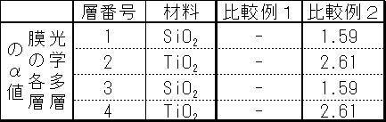
上記結果について、光学多層膜の層数と加重平均反射率の関係をまとめた。その結果を、表3及び図5に示した。

表3及び図5から明らかなように、本発明の発光装置の反射膜は、90.0%以上という優れた加重平均反射率を有した。詳細には、11層では91.3%という、かなり優れた加重平均反射率を有し、層数が増加するほど加重平均反射率は更に高くなり、21層以上では、94%を超え、非常に優れた加重平均反射率を有した。
11層の光学多層膜の各層のα値と加重平均反射率の関係をまとめた。その結果を、表4及び図6に示した。

21層の光学多層膜の各層のα値と加重平均反射率の関係をまとめた。その結果を、表5及び図7に示した。

表4、表5、図6、及び図7から明らかなように、α値が大きいほど、加重平均反射率は増加した。ただし、α値が、1.50を超えると加重平均反射率の増加はあまり見られなくなった。
21層の光学多層膜のα値が1.05以上の層の数と、加重平均反射率との関係をまとめた。その結果を表6及び図8に示した。

表6、及び図8から明らかなように、α値が1.05以上の層数が多いほど、加重平均反射率は高くなった。
21層の光学多層膜のα値が1.00以外の層の数と、加重平均反射率との関係をまとめた。その結果を表7及び図9に示した。

本発明の発光装置は、反射率が高いため、照明や表示のための光源へ好適に用いることができる。
1 発光装置
2 発光素子
3 反射膜
3a 金属膜
3b 光学多層膜
4 パッケージ
5 封止部
6 リードフレーム
7 ボンディングワイヤー
2 発光素子
3 反射膜
3a 金属膜
3b 光学多層膜
4 パッケージ
5 封止部
6 リードフレーム
7 ボンディングワイヤー
Claims (7)
- 発光素子と反射膜とを有する発光装置であって、
前記反射膜が、金属膜上に光学多層膜を積層した反射膜であり、かつ400nm~700nmの波長領域における平均反射率が90.0%以上であることを特徴とする発光装置。 - 光学多層膜の層数が、5層以上である請求項1に記載の発光装置。
- 光学多層膜が、下記式(1)で求められるαが1.05以上である層を有する請求項1から2のいずれかに記載の発光装置。
α=4×n×d/λ 式(1)
ここで、d(nm)は層の厚み、nは層の屈折率、λ(nm)は(λ1+λ2)/2を示す。λ1は200nm~1,000nmの波長領域における発光素子の発光波長において、ピーク波長の光強度の1/10となる波長のうちの最も短い波長を示し、λ2は200nm~1,000nmの波長領域における発光素子の発光波長において、ピーク波長の光強度の1/10となる波長のうちの最も長い波長を示す。 - 光学多層膜が、式(1)で求められるαが1.05以上である層を2層以上有する請求項3に記載の発光装置。
- 光学多層膜が、屈折率1.60~2.80の第一の層と、屈折率1.20~1.70の第二の層とが交互に積層した多層膜であり、前記第一の層と前記第二の層との屈折率差が0.1以上である請求項1から4のいずれかに記載の発光装置。
- 光学多層膜が、酸化チタンの層と酸化ケイ素の層とが交互に積層した多層膜である請求項1から5のいずれかに記載の発光装置。
- 発光素子が、発光ダイオードである請求項1から6のいずれかに記載の発光装置。
Applications Claiming Priority (2)
| Application Number | Priority Date | Filing Date | Title |
|---|---|---|---|
| JP2010-170890 | 2010-07-29 | ||
| JP2010170890A JP2012033633A (ja) | 2010-07-29 | 2010-07-29 | 発光装置 |
Publications (1)
| Publication Number | Publication Date |
|---|---|
| WO2012014606A1 true WO2012014606A1 (ja) | 2012-02-02 |
Family
ID=45529826
Family Applications (1)
| Application Number | Title | Priority Date | Filing Date |
|---|---|---|---|
| PCT/JP2011/064350 Ceased WO2012014606A1 (ja) | 2010-07-29 | 2011-06-23 | 発光装置 |
Country Status (2)
| Country | Link |
|---|---|
| JP (1) | JP2012033633A (ja) |
| WO (1) | WO2012014606A1 (ja) |
Families Citing this family (1)
| Publication number | Priority date | Publication date | Assignee | Title |
|---|---|---|---|---|
| JP5877992B2 (ja) * | 2010-10-25 | 2016-03-08 | 株式会社半導体エネルギー研究所 | 表示装置 |
Citations (3)
| Publication number | Priority date | Publication date | Assignee | Title |
|---|---|---|---|---|
| JP2006351808A (ja) * | 2005-06-15 | 2006-12-28 | Matsushita Electric Works Ltd | 発光装置 |
| JP2009164423A (ja) * | 2008-01-08 | 2009-07-23 | Nichia Corp | 発光素子 |
| JP2009238932A (ja) * | 2008-03-26 | 2009-10-15 | Panasonic Electric Works Co Ltd | 半導体発光素子およびそれを用いる照明装置 |
-
2010
- 2010-07-29 JP JP2010170890A patent/JP2012033633A/ja not_active Withdrawn
-
2011
- 2011-06-23 WO PCT/JP2011/064350 patent/WO2012014606A1/ja not_active Ceased
Patent Citations (3)
| Publication number | Priority date | Publication date | Assignee | Title |
|---|---|---|---|---|
| JP2006351808A (ja) * | 2005-06-15 | 2006-12-28 | Matsushita Electric Works Ltd | 発光装置 |
| JP2009164423A (ja) * | 2008-01-08 | 2009-07-23 | Nichia Corp | 発光素子 |
| JP2009238932A (ja) * | 2008-03-26 | 2009-10-15 | Panasonic Electric Works Co Ltd | 半導体発光素子およびそれを用いる照明装置 |
Also Published As
| Publication number | Publication date |
|---|---|
| JP2012033633A (ja) | 2012-02-16 |
Similar Documents
| Publication | Publication Date | Title |
|---|---|---|
| JP6374564B2 (ja) | 分布ブラッグ反射器を有する発光ダイオードチップ、及び分布ブラッグ反射器を有する発光ダイオードパッケージ | |
| JP6013555B2 (ja) | 発光ダイオードチップ及びそれを製造する方法 | |
| KR100765946B1 (ko) | 발광장치 | |
| CN100355108C (zh) | 有机电致发光器件 | |
| JPWO2011055440A1 (ja) | 表示装置 | |
| CN101809778B (zh) | 光电子器件 | |
| KR101344256B1 (ko) | 표시장치 | |
| US8487334B2 (en) | Semiconductor light emitting diode chip and light emitting device using the same | |
| US10084122B2 (en) | Light-emitting apparatus and method of manufacturing the same | |
| JP5855344B2 (ja) | 分布ブラッグ反射器を有する発光ダイオードチップ及びその製造方法 | |
| KR20120083497A (ko) | 유기 일렉트로루미네슨트 소자와 그것을 구비한 표시장치 | |
| JP2008251217A (ja) | 有機エレクトロルミネセンス素子 | |
| CN110148684A (zh) | 一种显示面板及显示装置 | |
| CN117542938A (zh) | 倒装发光二极管 | |
| CN1431852A (zh) | 显示装置的制造方法和显示装置 | |
| JP2016506015A (ja) | 透明導電性膜およびこれを含む有機発光素子 | |
| CN101499516B (zh) | 发光器件及其制造方法和显示单元 | |
| WO2012014606A1 (ja) | 発光装置 | |
| JP2007294438A (ja) | 有機el素子 | |
| KR100793314B1 (ko) | 다층 구조의 애노드 및 상기 애노드를 포함하는 상향 발광유기 발광소자 | |
| CN110323358B (zh) | 发光二极管及其制造方法和发光装置 | |
| JP2012059576A (ja) | 有機エレクトロルミネッセンス素子 | |
| JP2004247106A (ja) | 有機el素子および有機el素子の製造方法 | |
| KR100944915B1 (ko) | 유기 발광 다이오드 소자 | |
| KR102054528B1 (ko) | 투명 도전성막 및 이를 포함하는 유기 발광 소자 |
Legal Events
| Date | Code | Title | Description |
|---|---|---|---|
| 121 | Ep: the epo has been informed by wipo that ep was designated in this application |
Ref document number: 11812199 Country of ref document: EP Kind code of ref document: A1 |
|
| NENP | Non-entry into the national phase |
Ref country code: DE |
|
| 122 | Ep: pct application non-entry in european phase |
Ref document number: 11812199 Country of ref document: EP Kind code of ref document: A1 |