WO2012008554A1 - アモルファス導電性酸化物膜を形成するための前駆体組成物および方法 - Google Patents
アモルファス導電性酸化物膜を形成するための前駆体組成物および方法 Download PDFInfo
- Publication number
- WO2012008554A1 WO2012008554A1 PCT/JP2011/066165 JP2011066165W WO2012008554A1 WO 2012008554 A1 WO2012008554 A1 WO 2012008554A1 JP 2011066165 W JP2011066165 W JP 2011066165W WO 2012008554 A1 WO2012008554 A1 WO 2012008554A1
- Authority
- WO
- WIPO (PCT)
- Prior art keywords
- oxide film
- mol
- conductive oxide
- composition
- heating
- Prior art date
- Legal status (The legal status is an assumption and is not a legal conclusion. Google has not performed a legal analysis and makes no representation as to the accuracy of the status listed.)
- Ceased
Links
Images


Classifications
-
- H—ELECTRICITY
- H01—ELECTRIC ELEMENTS
- H01B—CABLES; CONDUCTORS; INSULATORS; SELECTION OF MATERIALS FOR THEIR CONDUCTIVE, INSULATING OR DIELECTRIC PROPERTIES
- H01B13/00—Apparatus or processes specially adapted for manufacturing conductors or cables
-
- H—ELECTRICITY
- H10—SEMICONDUCTOR DEVICES; ELECTRIC SOLID-STATE DEVICES NOT OTHERWISE PROVIDED FOR
- H10D—INORGANIC ELECTRIC SEMICONDUCTOR DEVICES
- H10D62/00—Semiconductor bodies, or regions thereof, of devices having potential barriers
- H10D62/80—Semiconductor bodies, or regions thereof, of devices having potential barriers characterised by the materials
- H10D62/86—Semiconductor bodies, or regions thereof, of devices having potential barriers characterised by the materials being Group II-VI materials, e.g. ZnO
-
- C—CHEMISTRY; METALLURGY
- C01—INORGANIC CHEMISTRY
- C01G—COMPOUNDS CONTAINING METALS NOT COVERED BY SUBCLASSES C01D OR C01F
- C01G55/00—Compounds of ruthenium, rhodium, palladium, osmium, iridium, or platinum
-
- C—CHEMISTRY; METALLURGY
- C01—INORGANIC CHEMISTRY
- C01G—COMPOUNDS CONTAINING METALS NOT COVERED BY SUBCLASSES C01D OR C01F
- C01G55/00—Compounds of ruthenium, rhodium, palladium, osmium, iridium, or platinum
- C01G55/002—Compounds containing ruthenium, rhodium, palladium, osmium, iridium or platinum, with or without oxygen or hydrogen, and containing two or more other elements
-
- H—ELECTRICITY
- H01—ELECTRIC ELEMENTS
- H01B—CABLES; CONDUCTORS; INSULATORS; SELECTION OF MATERIALS FOR THEIR CONDUCTIVE, INSULATING OR DIELECTRIC PROPERTIES
- H01B1/00—Conductors or conductive bodies characterised by the conductive materials; Selection of materials as conductors
- H01B1/06—Conductors or conductive bodies characterised by the conductive materials; Selection of materials as conductors mainly consisting of other non-metallic substances
- H01B1/08—Conductors or conductive bodies characterised by the conductive materials; Selection of materials as conductors mainly consisting of other non-metallic substances oxides
-
- H—ELECTRICITY
- H01—ELECTRIC ELEMENTS
- H01B—CABLES; CONDUCTORS; INSULATORS; SELECTION OF MATERIALS FOR THEIR CONDUCTIVE, INSULATING OR DIELECTRIC PROPERTIES
- H01B1/00—Conductors or conductive bodies characterised by the conductive materials; Selection of materials as conductors
- H01B1/20—Conductive material dispersed in non-conductive organic material
-
- H—ELECTRICITY
- H10—SEMICONDUCTOR DEVICES; ELECTRIC SOLID-STATE DEVICES NOT OTHERWISE PROVIDED FOR
- H10D—INORGANIC ELECTRIC SEMICONDUCTOR DEVICES
- H10D30/00—Field-effect transistors [FET]
- H10D30/60—Insulated-gate field-effect transistors [IGFET]
- H10D30/67—Thin-film transistors [TFT]
- H10D30/6729—Thin-film transistors [TFT] characterised by the electrodes
- H10D30/6737—Thin-film transistors [TFT] characterised by the electrodes characterised by the electrode materials
- H10D30/6739—Conductor-insulator-semiconductor electrodes
-
- H—ELECTRICITY
- H10—SEMICONDUCTOR DEVICES; ELECTRIC SOLID-STATE DEVICES NOT OTHERWISE PROVIDED FOR
- H10D—INORGANIC ELECTRIC SEMICONDUCTOR DEVICES
- H10D62/00—Semiconductor bodies, or regions thereof, of devices having potential barriers
- H10D62/40—Crystalline structures
- H10D62/402—Amorphous materials
-
- C—CHEMISTRY; METALLURGY
- C01—INORGANIC CHEMISTRY
- C01P—INDEXING SCHEME RELATING TO STRUCTURAL AND PHYSICAL ASPECTS OF SOLID INORGANIC COMPOUNDS
- C01P2002/00—Crystal-structural characteristics
- C01P2002/70—Crystal-structural characteristics defined by measured X-ray, neutron or electron diffraction data
- C01P2002/72—Crystal-structural characteristics defined by measured X-ray, neutron or electron diffraction data by d-values or two theta-values, e.g. as X-ray diagram
-
- C—CHEMISTRY; METALLURGY
- C01—INORGANIC CHEMISTRY
- C01P—INDEXING SCHEME RELATING TO STRUCTURAL AND PHYSICAL ASPECTS OF SOLID INORGANIC COMPOUNDS
- C01P2006/00—Physical properties of inorganic compounds
- C01P2006/40—Electric properties
-
- H—ELECTRICITY
- H10—SEMICONDUCTOR DEVICES; ELECTRIC SOLID-STATE DEVICES NOT OTHERWISE PROVIDED FOR
- H10D—INORGANIC ELECTRIC SEMICONDUCTOR DEVICES
- H10D30/00—Field-effect transistors [FET]
- H10D30/60—Insulated-gate field-effect transistors [IGFET]
- H10D30/67—Thin-film transistors [TFT]
- H10D30/674—Thin-film transistors [TFT] characterised by the active materials
- H10D30/6755—Oxide semiconductors, e.g. zinc oxide, copper aluminium oxide or cadmium stannate
-
- H—ELECTRICITY
- H10—SEMICONDUCTOR DEVICES; ELECTRIC SOLID-STATE DEVICES NOT OTHERWISE PROVIDED FOR
- H10P—GENERIC PROCESSES OR APPARATUS FOR THE MANUFACTURE OR TREATMENT OF DEVICES COVERED BY CLASS H10
- H10P14/00—Formation of materials, e.g. in the shape of layers or pillars
- H10P14/20—Formation of materials, e.g. in the shape of layers or pillars of semiconductor materials
- H10P14/26—Formation of materials, e.g. in the shape of layers or pillars of semiconductor materials using liquid deposition
- H10P14/265—Formation of materials, e.g. in the shape of layers or pillars of semiconductor materials using liquid deposition using solutions
-
- H—ELECTRICITY
- H10—SEMICONDUCTOR DEVICES; ELECTRIC SOLID-STATE DEVICES NOT OTHERWISE PROVIDED FOR
- H10P—GENERIC PROCESSES OR APPARATUS FOR THE MANUFACTURE OR TREATMENT OF DEVICES COVERED BY CLASS H10
- H10P14/00—Formation of materials, e.g. in the shape of layers or pillars
- H10P14/20—Formation of materials, e.g. in the shape of layers or pillars of semiconductor materials
- H10P14/29—Formation of materials, e.g. in the shape of layers or pillars of semiconductor materials characterised by the substrates
- H10P14/2901—Materials
- H10P14/2922—Materials being non-crystalline insulating materials, e.g. glass or polymers
-
- H—ELECTRICITY
- H10—SEMICONDUCTOR DEVICES; ELECTRIC SOLID-STATE DEVICES NOT OTHERWISE PROVIDED FOR
- H10P—GENERIC PROCESSES OR APPARATUS FOR THE MANUFACTURE OR TREATMENT OF DEVICES COVERED BY CLASS H10
- H10P14/00—Formation of materials, e.g. in the shape of layers or pillars
- H10P14/20—Formation of materials, e.g. in the shape of layers or pillars of semiconductor materials
- H10P14/34—Deposited materials, e.g. layers
- H10P14/3402—Deposited materials, e.g. layers characterised by the chemical composition
- H10P14/3434—Deposited materials, e.g. layers characterised by the chemical composition being oxide semiconductor materials
-
- H—ELECTRICITY
- H10—SEMICONDUCTOR DEVICES; ELECTRIC SOLID-STATE DEVICES NOT OTHERWISE PROVIDED FOR
- H10P—GENERIC PROCESSES OR APPARATUS FOR THE MANUFACTURE OR TREATMENT OF DEVICES COVERED BY CLASS H10
- H10P14/00—Formation of materials, e.g. in the shape of layers or pillars
- H10P14/20—Formation of materials, e.g. in the shape of layers or pillars of semiconductor materials
- H10P14/34—Deposited materials, e.g. layers
- H10P14/3451—Structure
- H10P14/3452—Microstructure
- H10P14/3454—Amorphous
Definitions
- the present invention relates to a precursor composition and method for forming an amorphous conductive oxide film.
- conductive oxides are widely used as conductive materials constituting electrodes, wirings, and the like.
- a crystalline oxide is used as the conductive oxide. That is, it is known that when the size of an electrode or wiring composed of a crystalline material is close to the crystal size, the conductivity is not continuous. Accordingly, the electrodes and the like need to have a size at least three times the crystal size.
- amorphous conductive oxides for example, IZO (indium-zinc composite oxide), IGZO (indium-gallium-zinc composite oxide), and the like are known. Conventionally, films made of these amorphous conductive oxides have been formed by vapor phase methods such as sputtering, laser ablation, and vapor deposition.
- the vapor phase method requires a heavy and expensive apparatus and the productivity of the film is low, so that the cost required for forming the film is a heavy burden.
- a technique for forming an amorphous conductive oxide film by a cheaper liquid phase process has been reported (CK Chen, et al., Journal of Display Technology, Vol. 5, No. 12, pp509-514 (2009)).
- a solution composition containing indium chloride, zinc chloride and acetonitrile as an oxide precursor is applied onto a substrate and heated to form an IZO film.
- the film obtained by this technique has a volume resistivity exceeding 1 ⁇ ⁇ cm, and therefore has insufficient conductivity, and has not yet been put into practical use.
- the volume resistivity needs to be 0.1 ⁇ ⁇ cm or less.
- amorphous IZO and IGZO have a problem of low thermal stability. Since these materials can maintain an amorphous state up to 500 ° C. and crystallization occurs at 500 to 600 ° C., these materials cannot be applied to electronic devices that require a processing temperature of 500 ° C. or higher. . Under the circumstances as described above, a method for forming a highly conductive and stable amorphous conductive oxide film by an inexpensive liquid phase process is desired.
- semiconductor elements such as diodes and transistors exhibit their functions by bonding between semiconductors exhibiting different types of conductivity such as pn junctions and pin junctions.
- Such semiconductors have long been manufactured using metalloid elements such as silicon and germanium.
- metalloid elements such as silicon and germanium.
- Such a material is expensive to manufacture and easily decomposes at a high temperature of 600 ° C. or higher, and is not necessarily satisfactory as a semiconductor material used industrially.
- an oxide semiconductor such as an In—Ga—Zn—O-based semiconductor can be prepared at a low temperature by a simple method such as a coating method, and there is no need to particularly control the ambient atmosphere during the preparation.
- the obtained thin film is expected as a material having various attractive properties such as optical transparency.
- a crystalline SnO thin film exhibiting p-type conductivity can be obtained by performing two-step annealing. Such a complicated manufacturing process is not industrially practical, and the crystalline SnO obtained has insufficient p-type semiconductor properties.
- the present invention has been made in view of the above circumstances, and an object thereof is to provide a simple conductive oxide film that exhibits high conductivity and that maintains an amorphous structure stably even when heated to a high temperature. It is to provide a precursor composition and method for forming by a liquid phase process. Another object of the present invention is to provide a precursor composition and method for forming a conductive oxide film that exhibits good semiconductivity, preferably p-type conductivity, by a simple liquid phase process. It is in. According to the present invention, the above objects and advantages of the present invention are as follows.
- amorphous conductive oxide film forming composition At least one selected from the group consisting of lanthanoid (except cerium) carboxylate, nitrate and sulfate, and ruthenium, iridium or rhodium carboxylate, nitrosyl carboxylate, nitrosyl nitrate and nitrosyl sulfate
- amorphous conductive oxide film forming composition containing at least one selected from the group consisting of: a solvent containing at least one selected from the group consisting of carboxylic acids, alcohols and ketones.
- precursor composition Sometimes referred to as “precursor composition”).
- a method for forming an amorphous conductive oxide film which includes a step of applying the above precursor composition on a substrate to form a coating film and heating the coating film in an oxidizing atmosphere.
- FIG. 1 is an X-ray diffraction chart after heating at 370 ° C. measured in Example 1.
- FIG. FIG. 2 is an X-ray diffraction chart after additional heating at 500 ° C. measured in Example 1.
- FIG. 3 is an X-ray diffraction chart after additional heating at 550 ° C. measured in Example 1.
- 4 is an X-ray diffraction chart after additional heating at 600 ° C. measured in Example 1.
- FIG. FIG. 5 is an X-ray diffraction chart after additional heating at 650 ° C. measured in Example 1.
- 6 is an X-ray diffraction chart after additional heating at 800 ° C. measured in Example 1.
- FIG. FIG. 7 is an atomic force microscope photograph taken in Example 3.
- FIG. 7A shows a case where no chelating agent is contained, and FIG. 7B shows a case containing a chelating agent.
- FIG. 8 is a thermogravimetric analysis chart of the precursor composition of the present invention (containing no chelating agent) measured in Example 4.
- FIG. 9 is a thermogravimetric analysis chart of the precursor composition of the present invention (containing a chelating agent) measured in Example 4.
- FIG. 10 is an X-ray diffraction chart after additional heating of the oxide film formed in Example 6 at each temperature.
- FIG. 11 is an atomic force microscope photograph after additional heating at 500 ° C. taken in Example 6.
- FIG. 12 is an X-ray diffraction chart of each oxide film formed in Example 8.
- FIG. 13 is an atomic force micrograph of the transfer pattern taken in Example 9.
- FIG. 14 is an X-ray diffraction chart of each oxide film formed in Example 10.
- FIG. 15 is an X-ray diffraction chart of the Ce—Ru oxide film formed in Example 10.
- FIG. 16 is an X-ray diffraction chart of the La—Ir oxide film formed in Example 11.
- FIG. 17 is an X-ray diffraction chart of the La—Rh oxide film formed in Example 11.
- FIG. 18 is a specific resistance-temperature curve of the La—Ru oxide film formed in Example 12.
- composition for forming an amorphous conductive oxide film (precursor composition) of the present invention is as described above. At least one selected from the group consisting of lanthanoid (except cerium) carboxylate, nitrate and sulfate, and ruthenium, iridium or rhodium carboxylate, nitrosyl carboxylate, nitrosyl nitrate and nitrosyl sulfate And a solvent containing at least one selected from the group consisting of carboxylic acids, alcohols and ketones.
- lanthanoids excluding cerium are sometimes collectively referred to simply as “lanthanoids”.
- the symbol “Ln” is used when a lanthanoid having such a meaning is represented by a chemical formula.
- ruthenium, iridium or rhodium may be collectively referred to simply as “platinum group elements”.
- platinum group element in such a meaning is expressed by a chemical formula, the symbol “M” is used.
- any of the elements having atomic numbers 57 and 59 to 71 can be preferably used. CE is excluded.
- the lanthanoid at least one selected from the group consisting of lanthanum, praseodymium, neodymium, samarium, europium and gadolinium is preferably used, and lanthanum is more preferably used.
- the lanthanoid carboxylate and the platinum group element carboxylate are each preferably a salt of a carboxylic acid having an alkyl group having 1 to 10 carbon atoms, and a carboxyl having an alkyl group having 1 to 8 carbon atoms.
- An acid salt is more preferable, and examples thereof include acetate, propionate, butyrate, valerate, and 2-ethylhexanoate.
- the carboxylates may be anhydrous salts or hydrated salts.
- the lanthanoid nitrate and the lanthanoid sulfate may be anhydrous or hydrated, respectively.
- the nitrosylcarboxylate of the platinum group element is generally a salt represented by the chemical formula M (NO) (OOCR) 3 (where R is an alkyl group).
- R is preferably an alkyl group having 1 to 10 carbon atoms, and more preferably an alkyl group having 1 to 8 carbon atoms.
- the nitrosyl carboxylate is preferably, for example, nitrosyl acetate, nitrosyl propionate, nitrosyl butyrate, nitrosyl valerate, nitrosyl-2-ethylhexanoate, etc., and more preferably nitrosyl acetate. preferable.
- These nitrosylcarboxylates may be anhydrous salts or hydrated salts.
- the platinum group elements nitrosyl nitrate and nitrosyl sulfate are salts generally represented by the chemical formulas M (NO) (NO 3 ) 3 and M 2 (NO) 2 (SO 4 ) 3 , respectively. These may be anhydrous salts or hydrated salts.
- the lanthanoid salt it is preferable to use at least one selected from the group consisting of lanthanoid carboxylates and lanthanoid nitrates, including lanthanum acetate, lanthanum 2-ethylhexanoate and lanthanum nitrate, and 3 It is more preferable to use at least one selected from the group consisting of salts obtained by replacing lanthanum in the salt with praseodymium, neodymium, samarium, europium or gadolinium, and in particular, lanthanum acetate, lanthanum 2-ethylhexanoate and lanthanum nitrate It is preferable to use at least one selected from the group consisting of: As the platinum group element salt, it is preferable to use at least one selected from the group consisting of a carboxylate salt of a platinum group element and a nitrosyl carboxylate, and in particular, ruthenium 2-ethyl
- the use ratio of the lanthanoid salt and the platinum group element salt in the precursor composition of the present invention is appropriately set according to the desired lanthanoid / platinum group element ratio (Ln / M ratio) in the conductive oxide film to be formed.
- the film in which the Ln / M ratio (molar ratio) in the composition is formed is maintained almost as it is. Therefore, the Ln / M ratio in the composition can be, for example, 0.5 (mol / mol) or more, depending on the desired value of the Ln / M ratio in the film, and can be 0.6 to 2.0 ( Mol / mol), preferably 0.7 to 1.5 (mol / mol), more preferably 0.8 to 1.3 (mol / mol).
- the solvent contained in the precursor composition of the present invention contains at least one selected from the group consisting of carboxylic acids, alcohols and ketones.
- the solvent in the present invention may contain at least one selected from the group consisting of aliphatic hydrocarbons, alicyclic hydrocarbons, aromatic hydrocarbons, esters and ethers.
- the carboxylic acid is preferably a carboxylic acid having an alkyl group having 1 to 10 carbon atoms, and more preferably a carboxylic acid having an alkyl group having 2 to 8 carbon atoms.
- carboxylic acids include propionic acid, n-butyric acid, isobutyric acid, n-hexanoic acid, n-octanoic acid and 2-ethylhexanoic acid.
- the alcohol is preferably a primary alcohol, such as methanol, ethanol, propanol, isopropanol, 1-butanol, sec-butanol, t-butanol, methoxymethanol, ethoxymethanol, 2-methoxyethanol, 2-ethoxyethanol and the like. Can do.
- the ketone is preferably a ketone having 3 to 10 carbon atoms, and more preferably a ketone having 4 to 7 carbon atoms.
- This carbon number is the number including the carbon of the carbonyl group.
- ketones include methyl ethyl ketone, methyl isobutyl ketone, and diethyl ketone.
- aliphatic hydrocarbon for example, hexane, octane, etc .
- alicyclic hydrocarbon examples include cyclohexane
- aromatic hydrocarbon examples include benzene, toluene, xylene and the like
- Examples of the ester include methyl acetate, ethyl acetate, methyl propionate, ethyl propionate, methyl butyrate, ethyl acetate, methyl 2-ethylhexanoate, ethyl 2-ethylhexanoate and the like
- the ether examples include diethyl ether, dibutyl ether, ethylene glycol dimethyl ether, ethylene glycol diethyl ether, ethylene glyco
- the solvent in the present invention contains at least one selected from the group consisting of carboxylic acids, alcohols and ketones.
- the content ratio of at least one selected from the group consisting of carboxylic acid, alcohol and ketone in the solvent of the present invention is 50% by weight with respect to the total amount of the solvent from the viewpoint of solubility and long-term stability of the composition. % Or more, and more preferably 75% by weight or more.
- a non-aqueous solvent that does not substantially contain water.
- substantially free of water does not exclude the presence of a trace amount of water as an impurity contained in a hydrophilic solvent or the like, This includes the case where the water content in the solvent is reduced as much as possible.
- the water content in the solvent is preferably 1% by weight or less, and more preferably 0.1% by weight or less.
- the precursor composition of the present invention contains the lanthanoid salt, platinum group element salt and solvent as described above as essential components, but may contain other components as long as the effects of the present invention are not impaired. Examples of such other components include chelating agents.
- the chelating agent can be contained in the precursor composition of the present invention for the purpose of further improving the surface smoothness of the formed film.
- the chelating agent is coordinated to the lanthanoid salt and the platinum group element salt in a chelating manner, and the core of the thermal decomposition of the salt is delayed by delaying the decomposition of these salts in the heating step in the film formation described later.
- the surface of the film is assumed to be smoother.
- the chelating agent having such a function include compounds having at least two groups selected from the group consisting of an amino group and a hydroxyl group.
- chelating agents include compounds having two or more amino groups such as ethylenediamine and polyethyleneamine; Examples of compounds having two or more hydroxyl groups include ethylene glycol and glycerin; Examples of the compound having both an amino group and a hydroxyl group include monoethanolamine, and at least one selected from these can be preferably used.
- the use ratio thereof may be 3 mol or more with respect to 1 mol in total of the lanthanoid atom and the platinum group element atom in the composition. Preferably, the amount is 5 to 20 mol.
- composition for forming an amorphous conductive oxide film (precursor composition) of the present invention can be prepared by mixing and dissolving components other than the solvent in the solvent as described above. At this time, the solvent and each component may be mixed and dissolved at a time, each component may be added sequentially in the solvent, or several components obtained by dissolving each component separately in the solvent. It may be by a method of mixing solutions, or by other appropriate methods. In preparing the precursor composition of the present invention, heating may be performed as necessary.
- the precursor composition of the present invention preferably has its liquidity set in an acidic region, more preferably has a pH of 6.5 or less, and particularly preferably has a pH of 3-6.
- the solid content concentration of the precursor composition of the present invention (ratio of the total weight of the lanthanoid salt and platinum group element salt in the composition to the total weight of the composition) is preferably 0.1 to 10% by weight. More preferably, the content is 0.5 to 6% by weight.
- the prepared composition may be used after being filtered through a filter having an appropriate pore size. As described above, since the lanthanoid salt and the platinum group element salt that are components of the precursor composition of the present invention may each be a hydrated salt, the precursor composition of the present invention contains water immediately after preparation. Also good.
- the solvent contains at least one selected from the group consisting of hydrophilic carboxylic acids, alcohols and ketones, it may absorb moisture during use or storage of the composition.
- the precursor composition of the present invention can be stored for a long period of time without controlling the water content in the composition. Therefore, the precursor composition of the present invention can form a highly conductive oxide film by a simple method as described later, and its preparation cost and storage cost are greatly reduced. This contributes to reducing the manufacturing cost of electrical devices.
- it when applying the precursor composition of this invention to a semiconductor element, it is preferable that it does not contain water substantially.
- substantially free of water does not exclude the presence of trace amounts of water as impurities and water as crystal water contained in hydrophilic raw materials and the like.
- moisture content in a composition is reduced as much as possible by the normal effort made above is included.
- the water content in the composition is, for example, preferably 5% by weight or less, more preferably 1% by weight or less, and particularly preferably 0.5% by weight or less.
- substrate used for the method of this invention For example, quartz; Glass, such as borosilicate glass, soda glass, quartz glass; Plastic; Carbon; Silicone resin; Silicon; Gold, silver, copper, nickel, Metals such as titanium, aluminum, tungsten, etc .; substrates made of glass, plastics, silicon, etc. having these metals or their oxides, mixed oxides (such as ITO) or silicon oxide on their surfaces can be used.
- an appropriate application method such as a spin coating method, a roll coating method, a curtain coating method, a dip coating method, a spray method, or a droplet discharge method can be employed.
- the coating film can be formed on the substrate by removing the solvent from the liquid coating film comprising the precursor composition as necessary. At this time, even if some solvent remains in the coating film, the effect of the present invention is not diminished.
- it can be performed, for example, by standing at room temperature to 450 ° C. for about 1 to 30 minutes.
- the coating film thus formed is then heated under an oxidizing atmosphere. Heating in an oxidizing atmosphere can be realized preferably by performing a heating operation in a gas containing oxygen.
- a gas containing oxygen As the substrate containing oxygen, air, oxygen, or the like is preferably used.
- the gas at the time of heating can be made into arbitrary pressure, for example, can be heated at 5 ⁇ 10 4 to 1 ⁇ 10 6 Pa.
- the temperature at the time of heating is preferably 370 ° C. or higher, more preferably 400 ° C. or higher, and more preferably 500 ° C. or higher from the viewpoint of imparting appropriate conductivity to the formed film. Further preferred.
- the conductive oxide film obtained by the method of the present invention does not crystallize even when the heating temperature is high, or is very difficult to crystallize. Therefore, the conductive oxide film is not limited to the crystal size regardless of the heating temperature. A functional film can be formed. However, since the crystallization may occur slightly when the Ln / M ratio in the film is small, the upper limit of the heating temperature is preferably set according to the Ln / M ratio from the viewpoint of avoiding such crystallization. .
- the Ln / M ratio in the film is 0.9 to 2.0 (mol / mol) (that is, the Ln / M ratio in the composition is 0.9 to 2.0 (mol / mol)) ) Does not cause crystallization even when the heating temperature is 750 ° C .;
- the Ln / M ratio in the film is 0.8 (mol / mol) or more and less than 0.9 (mol / mol)
- crystallization does not occur even when the heating temperature is set to 700 ° C .
- the Ln / M ratio in the film is 0.6 (mol / mol) or more and less than 0.8 (mol / mol)
- crystallization does not occur even when the heating temperature is 650 ° C.
- the temperature is not higher than these temperatures depending on the / M ratio.
- the heating time is preferably 3 minutes or more, more preferably 10 minutes or more.
- an oxide film having a sufficiently high conductivity can be formed by heating at the above temperature for the above time, so there is no practical advantage of continuing the heating for a long time.
- the heating time is preferably 2 hours or less.
- the conductive oxide film may be formed by performing the coating of the precursor composition, the removal of an arbitrary solvent, and the heating process only once (one cycle) as described above, or this cycle is repeated a plurality of times.
- a conductive oxide film may be formed by an overcoating method.
- the thickness of the amorphous conductive oxide film thus formed should be appropriately set according to the purpose of application, and can be set to, for example, 20 to 500 nm.
- Method for forming patterned amorphous conductive oxide film In the method for forming an amorphous conductive oxide film as described above, after the precursor composition of the present invention is formed on a substrate to form a coating film, a patterned mold is disposed on the coating film to form the substrate.
- a patterned amorphous conductive oxide film can be formed by passing a coating film between the mold and the patterned mold and then heating the coating film in an oxidizing atmosphere. That is, the method for forming such a patterned conductive oxide film is as follows: Applying the precursor composition of the present invention on a substrate to form a coating film, A method comprising: placing a pattern mold on the coating film, sandwiching the coating film between the substrate and the pattern mold, and heating the coating film in an oxidizing atmosphere. It is. In the present specification, such a method for forming a patterned film may be hereinafter referred to as a “nanoimprint method”.
- the substrate used here, the method of applying the precursor composition onto the substrate, and the thickness of the coating film formed are the same as those in the method of forming the amorphous conductive oxide film.
- a mold made of the same material as described above can be used as the material constituting the substrate.
- silicon, quartz, silicon with an oxide film, silicone resin from the viewpoints of good workability and the ability to form fine patterns, and good release of the patterned oxide film.
- PDMS polydimethylsiloxane
- metal for example, nickel etc.
- Examples of the pattern of the pattern mold include a line and space pattern, a columnar shape or a polygonal column shape (for example, a quadrangular columnar shape), a conical shape or a polygonal pyramid shape (for example, a quadrangular pyramid shape), or a shape obtained by cutting them in a plane.
- a mirror surface may be used.
- the method for forming a patterned amorphous conductive oxide film of the present invention it is possible to form a patterned film in which any fine pattern of the patterned mold as the parent pattern is preferably transferred,
- the width is, for example, 10 nm or more, preferably 50 nm or more
- the aspect ratio is a value obtained by dividing the line height by the line or space width in the line-and-space pattern, and in the protrusion, the height of the protrusion is divided by the diameter of the protrusion or the length of one side.
- the value means the value obtained by dividing the depth of the hole by the diameter of the hole or the length of one side.
- a patterned mold is then placed on the coating film formed on the substrate as described above, and the coating film is sandwiched between the substrate and the patterned mold by pressing and pressing it as necessary. can do.
- the pressing pressure when the pattern mold is pressed is preferably 0.1 to 10 MPa.
- the release agent examples include surfactants (for example, fluorine-based surfactants, silicone-based surfactants, nonionic surfactants, etc.), fluorine-containing diamond-like carbon (F-DLC), and the like.
- surfactants for example, fluorine-based surfactants, silicone-based surfactants, nonionic surfactants, etc.
- F-DLC fluorine-containing diamond-like carbon
- the heating of the coating film may be performed while the coating film is sandwiched between the substrate and the pattern mold, or may be performed after removing the pattern mold on the coating film.
- the heating temperature, heating time, and oxidizing atmosphere are the same as those in the method for forming the amorphous conductive oxide film. Even when heating is performed with the coating film sandwiched between the substrate and the pattern mold, if the surrounding atmosphere is an oxidizing atmosphere, a sufficiently highly conductive oxide film is formed. be able to.
- Amorphous conductive oxide film or a patterned amorphous conductive oxide film can be formed.
- Amorphous conductive oxide films (including patterned ones) formed by the method of the present invention have high conductivity.
- the volume resistivity can be, for example, 1.0 ⁇ ⁇ cm or less, preferably 0.5 ⁇ ⁇ cm or less, and further 0.1 ⁇ ⁇ cm. cm or less, particularly 0.05 ⁇ ⁇ cm or less.
- the amorphous conductive oxide film (including the patterned one) formed by the method of the present invention does not crystallize even when heated to a high temperature, the heating temperature during the electronic device manufacturing process Regardless, it is possible to easily form fine electrodes, wirings, and the like without restrictions on crystal size. Therefore, the amorphous conductive oxide film formed by the method of the present invention can be suitably applied to various electronic devices, and can be used as a material such as a gate electrode of a thin film transistor.
- composition for forming conductive oxide film ⁇ Preparation of composition for forming conductive oxide film>
- lanthanum 2-ethylhexanoate a commercial product (anhydrous salt, purity 99% by weight) manufactured by Rare Earth products, Inc .
- Preparation Examples 2-6 In Preparation Example 1 above, the amount of the lanthanum 2-ethylhexanoate solution mixed with 2 g of the ruthenium 2-ethylhexanoate solution was 1.2 g (Preparation Example 2), 1.4 g (Preparation Example 3), 1.6 g ( The molar ratio of La / Ru was 0.6, 0.7, 0 in the same manner as in Preparation Example 1 except that Preparation Example 4), 1.8 g (Preparation Example 5) and 2.0 g (Preparation Example 6) were used. 0.8, 0.9 and 1.0 (mol / mol) compositions were prepared, respectively.
- Preparation Example 7 In a 13.5 mL glass bottle, 1 g of the composition having a La / Ru ratio of 0.9 (mol / mol) obtained in Preparation Example 5 was charged. Next, when 0.30 g of monoethanolamine was added dropwise thereto, a precipitate was observed. This mixture and a glass bottle were heated on a hot plate at 150 ° C. for 40 minutes to obtain a dark brown solution. This was allowed to cool to room temperature, and 1.30 g of 1-butanol was added to the viscous solution for dilution. As a result, the ratio of La / Ru was 0.9 (mol / mol). A composition containing ethanolamine was prepared.
- Example 1 ⁇ Formation and evaluation of conductive oxide film> Example 1
- the influence of the La / Ru ratio and the heating temperature on the crystallinity of the obtained oxide was examined.
- the oxide film after X-ray diffraction measurement was further heated at 500 ° C. for 30 minutes in an oxygen stream at a flow rate of 0.2 L (STP) / min, and then X-ray diffraction was measured again.
- the heating temperature and time were set to 550 ° C. for 30 minutes, 600 ° C. for 10 minutes, 650 ° C.
- X-ray diffraction charts measured after heating at 500 ° C., 550 ° C., 600 ° C., 650 ° C., and 800 ° C. are shown in FIGS.
- FIGS. 7A and 7B The number of cycles of spin coating and heating operations was repeated. Except for a total of 3 cycles, an oxide film having a thickness of about 100 nm was obtained on the substrate in the same manner as (1) above, and the volume resistivity after heating at 370 ° C. and after additional heating at 500 ° C. was measured. Each volume resistivity measured above is shown in Table 2.
- (3) Evaluation of surface roughness of oxide film The oxide film after additional heating at 500 ° C. obtained in the above (1) and (2) was measured with an atomic force microscope, and the root mean square roughness (RMS) was examined. Atomic force microscope photographs taken here are shown in FIGS. 7A and 7B, respectively.
- TG thermogravimetric analysis
- Measuring apparatus Model name “TG-DTA6200” manufactured by SII Nano Technology Supply gas: Air, 300 mL / min Measurement temperature range: 25 ⁇ 600 °C Temperature increase rate: 10 ° C / min Sample: The composition for forming a conductive oxide film was taken as it was in an aluminum measurement pan without removing the solvent, and this was used as a sample. Sample weight: About 15 mg was used after precise weighing. The rapid weight loss observed from the start of measurement in FIG. 8 to about 140 ° C. and from the start of measurement in FIG. When the temperature was further increased, the sample weight was reduced to about 370 ° C., and then became a constant value.
- Example 5 the constituent element ratio of the formed oxide film was examined.
- a La / Ru ratio obtained in Preparation Example 7 was 0.9 (mol / mol), and a composition containing a chelating agent was rotated at a rotational speed of 2
- heating was performed on a hot plate at 370 ° C. for 5 minutes to obtain an oxide film.
- This spin coating and heating operation was repeated for a total of 3 cycles, and a coating film was repeatedly applied on the substrate, thereby obtaining an oxide film having a thickness of 100 nm on the substrate.
- This oxide film was further heated at 550 ° C.
- the formed film contains significant amounts of C and H in addition to La, Ru and O, it is a conductive film having a novel composition containing an organic component in addition to the oxide.
- composition for forming conductive oxide film a commercial product (1.5 hydrate) manufactured by Kanto Chemical Co., Inc .;
- ruthenium nitrosyl acetate a commercial product (anhydrous salt) manufactured by Alfa Aesar;
- lanthanum nitrate a commercial product (hexahydrate) manufactured by Wako Pure Chemical Industries, Ltd .;
- lanthanum chloride a commercial product (7 water salt, purity ⁇ 95%) manufactured by Kanto Chemical Co., Inc .;
- As the ruthenium chloride a commercial product (trihydrate) manufactured by Kanto Chemical Co., Inc.
- Example 6 A composition having a La concentration and a Ru concentration of 0.067 mol / kg was prepared.
- ⁇ Formation and evaluation of conductive oxide film> Example 6 In this example, the conductivity, crystallinity, and surface smoothness of oxide films formed when acetate and nitrosyl acetate were used as the lanthanoid salt and ruthenium salt, respectively, were examined.
- the composition obtained in Preparation Example 8 above was spin-coated on a 20 mm ⁇ 20 mm silicon substrate having an oxide film on the surface under the conditions of 2,000 rpm and 25 seconds, and then heated on a hot plate at 150 ° C. 6 After sequentially heating for 1 minute on a second and 250 ° C. hot plate, the substrate was further heated at 400 ° C.
- the oxide film after these various measurements was further heated at 550 ° C. for 10 minutes in an oxygen stream at a flow rate of 0.2 L (STP) / min, and then volume resistivity and X-ray diffraction were measured again. Then, for the oxide film after the volume resistivity and X-ray diffraction remeasurement, the heating temperature and time were set to 700 ° C. for 10 minutes, 750 ° C. for 10 minutes, 800 ° C. for 10 minutes, and 850 ° C. for 10 minutes in the same manner as above. Additional heating was performed sequentially, and volume resistivity and X-ray diffraction were measured after additional heating at each temperature. Each volume resistivity after additional heating at 500 to 800 ° C.
- each X-ray diffraction chart after additional heating at 500 ° C., 550 ° C., 750 ° C., 800 ° C. and 850 ° C. is shown in FIG. Indicated. Further, an atomic force microscope image observed after additional heating at 500 ° C. is shown in FIG. From the results of the X-ray chart and the results of Table 3 below, the oxide film formed from this composition is stably maintained in an amorphous state up to 800 ° C., and exhibits high conductivity up to this temperature. It was confirmed.
- Example 7 the conductivity of an oxide film formed when nitrate and nitrosyl nitrate were used as the lanthanoid salt and ruthenium salt, respectively, was examined.
- the composition obtained in Preparation Example 9 was spin-coated on a 20 mm ⁇ 20 mm silicon substrate having an oxide film on the surface under the conditions of 2,000 rpm and 25 seconds, and then heated on a hot plate at 150 ° C. 6 After sequentially heating for 1 minute on a second plate at 250 ° C. for 2 minutes, the film was further heated at 400 ° C. for 5 minutes to obtain an oxide film. This spin coating, sequential heating and additional heating cycles were repeated three times in total to obtain an oxide film having a thickness of 200 nm.
- the volume resistivity of the oxide film obtained here was measured.
- the oxide film after the volume resistivity measurement was further heated at 550 ° C. for 10 minutes in an oxygen stream at a flow rate of 0.2 L (STP) / min, and then the volume resistivity was measured.
- the oxide film was further heated at 700 ° C. for 10 minutes in an oxygen stream at a flow rate of 0.2 L (STP) / min, and then the volume resistivity was measured again.
- Table 3 shows the volume resistivity values measured above. Comparative Example 1 In this comparative example, the conductivity of the oxide film formed when chlorides were used as the lanthanoid salt and ruthenium salt was examined.
- Preparation of composition for forming conductive oxide film Preparation Examples 10-12 Prepared except that the amount of lanthanum acetate 1.5 hydrate used in Preparation Example 8 was changed to 0.360 g (Preparation Example 10), 0.420 g (Preparation Example 11), and 0.480 g (Preparation Example 12), respectively. In the same manner as in Example 8, compositions having a La / Ru molar ratio of 1.2, 1.4 and 1.6 (mol / mol) were prepared, respectively.
- Example 8 In this example, an oxide conductive film was investigated when the La / Ru molar ratio exceeded 1.0.
- Each of the compositions obtained in Preparation Examples 10 to 12 above was spin-coated on a 20 mm ⁇ 20 mm silicon substrate having an oxide film on the surface under the conditions of 2,000 rpm for 25 seconds, and then 150 ° C. After sequentially heating for 6 seconds on a hot plate, for 1 minute on a hot plate at 250 ° C., and for 6 seconds on a hot plate at 400 ° C., heating was further performed at 450 ° C. for 5 minutes to obtain oxide films.
- Example 9 a patterned conductive oxide film was formed by the nanoimprint method using the composition for forming a conductive oxide film of the present invention.
- the nanoimprint experiment was performed using a nanoimprint experimental apparatus (prototype) with a press machine.
- This nanoimprint experimental apparatus with a press mainly comprises a pedestal, a mold holder, and two metal plates for pressing.
- Each of the two metal plates for pressing is provided with a heating device and a temperature controller, and a pedestal, a mold holder and the like sandwiched between them can be heated to 200 ° C.
- These two metal plates for pressing can press a pedestal, a mold holder, etc.
- the coating was formed by spin coating at a rotation speed of 2,000 rpm and a rotation time of 25 seconds, and then heating at 150 ° C. for 6 seconds.
- the silicon wafer having this coating was mounted on a nanoimprint experimental apparatus equipped with a press machine, and a heat treatment was performed at 200 ° C. for 5 minutes in a state where a TEOS processed substrate mold was pressed onto the coating at a pressure of 5 MPa. After standing to cool, the pressure is removed, the silicon wafer and the TEOS processed substrate mold having the coated film after pressing and heating are taken out, and the TEOS processed substrate mold is gently peeled to form the pattern of the TEOS processed substrate mold. A transferred pattern was obtained. This pattern was further heated at 550 ° C.
- the conductive oxide film according to the present invention is stably maintained in an amorphous state without being crystallized even when heated at a high temperature, so that distortion and deformation accompanying crystallization do not occur, and the crystal size is limited.
- a patterned conductive oxide film in which a fine pattern is accurately transferred can be easily formed.
- the patterned conductive oxide film according to the present invention does not crystallize even when heated after formation, and does not cause distortion or deformation. Therefore, the patterned conductive oxide film has a shape throughout the entire process of manufacturing an electronic device that requires element annealing. Excellent stability and high conductivity is maintained.
- La-ac Lanthanum acetate 1.5 hydrate (99.99%, manufactured by Kanto Chemical Co., Inc.) Ce-ac: cerium acetate (III) monohydrate (99.99%, manufactured by Kanto Chemical Co., Inc.) Pr-ac: praseodymium (III) acetate hydrate (99.9%, manufactured by Wako Pure Chemical Industries, Ltd.) Nd-ac: Neodymium acetate monohydrate (99.9%, manufactured by Wako Pure Chemical Industries, Ltd.) Sm-ac: Samarium acetate tetrahydrate (99.9%, manufactured by Wako Pure Chemical Industries, Ltd.) Eu-ac: Europium acetate (III) hydrated salt (99.9%, manufactured by Wako Pure Chemical Industries, Ltd.) Gd-ac: gadolinium (III) acetate hydrate (99.9%, manufactured by Aldrich), Tb-ac: terbium acetate (III) tetrahydrate (99.9%, manufactured by Wa
- compositions obtained in Preparation Examples 13 to 25 above were spin-coated on a 20 mm ⁇ 20 mm silicon substrate having an oxide film on the surface under the conditions of 2,000 rpm and 25 seconds, respectively, and then heated at 150 ° C. After sequentially heating on the plate for 6 seconds and on a hot plate at 250 ° C. for 1 minute, the plate was further heated at 400 ° C. for 5 minutes to obtain an oxide film having a thickness of about 20 nm. This spin coating, sequential heating and additional heating cycles were repeated three times in total to obtain an oxide film having a thickness of about 60 nm. The volume resistivity of the oxide film obtained here was measured. The oxide film after the volume resistivity measurement was further heated at 500 ° C.
- FIG. 15 shows X-ray diffraction charts of the experimental example using cerium as the lanthanoid after additional heating at 550 ° C. and after additional heating at 650 ° C. From these experimental results, when cerium was used as the lanthanoid, ruthenium oxide (RuO) even after additional heating at 550 ° C. 2 ) Crystallinity is seen and the volume resistivity is large, It can be seen that when a material other than cerium is used, no crystallinity is observed even after additional heating at 650 ° C., and the volume resistivity is small.
- RuO ruthenium oxide
- the volume resistivity is small when the lanthanoid is praseodymium, neodymium, samarium, europium or gadolinium.
- Example 11 the effect of using iridium or rhodium instead of ruthenium in a lanthanoid-ruthenium oxide film was examined. Except for using each of the compositions obtained in Preparation Examples 26 and 27, the composition was spin-coated on a silicon substrate having an oxide film on the surface, as in Example 10 above. The sequential heating cycle at 400 ° C. was repeated three times to obtain an oxide film having a thickness of about 60 nm. The volume resistivity of the oxide film obtained here was measured.
- the lanthanum-iridium oxide film is 500 ° C. for 30 minutes, 550 ° C. for 30 minutes, and 600 ° C. for 10 minutes. And additional heating at 650 ° C. for 10 minutes sequentially, For the lanthanum-rhodium oxide film, additional heating was sequentially performed at 500 ° C. for 10 minutes, 600 ° C. for 10 minutes, 700 ° C. for 10 minutes, 800 ° C. for 10 minutes, and 850 ° C. for 5 minutes. At this time, the volume resistivity of the oxide film was measured after additional heating at a temperature of 700 ° C. or lower.
- X-ray diffraction of the oxide film after additional heating at 500 ° C. and 650 ° C. was measured.
- the X-ray diffraction of the oxide film before additional heating (after 400 degreeC heating) and after additional heating in each temperature was measured.
- Each volume resistivity measured above is shown in Table 7, an X-ray diffraction chart of the lanthanum-iridium oxide film is shown in FIG. 16, and an X-ray diffraction chart of the lanthanum-rhodium oxide film is shown in FIG.
- Table 7 shows that the lanthanum-iridium oxide film has 10 -2 It was found to exhibit a volume resistivity on the order of ⁇ ⁇ cm. When the lanthanum-rhodium oxide film is heated at a temperature of 500 ° C. or higher, 10 -1 The volume resistivity was in the order of ⁇ ⁇ cm. It was also found that this lanthanum-rhodium oxide film maintained an amorphous state even when heated to 800 ° C. (FIG. 17). ⁇ Semiconductor property of conductive oxide film, constituent element ratio and carrier type> Example 12 In this example, it was confirmed that the lanthanum-ruthenium oxide film has semiconductor properties.
- composition prepared in the same manner as in Preparation Example 8 (a composition in which the La / Ru ratio is 1.0 (mol / mol) and the La concentration and the Ru concentration are each 0.067 mol / kg), Except for using a quartz glass substrate as the substrate, the composition was spin-coated on the substrate in the same manner as in Example 6, and then the sequential heating cycle at 150 ° C., 250 ° C. and 400 ° C. was repeated 5 times to obtain the film thickness. An oxide film of about 100 nm was obtained. Next, additional heating at 500 ° C. for 10 minutes was performed in an oxygen stream at a flow rate of 0.2 L (STP) / min to obtain an oxide film having a heating temperature of 500 ° C.
- STP flow rate
- Example 13 The same RBS / HFS as in Example 5 above, except that a silicon wafer having an oxide film on the surface was used as the substrate, and a film obtained by forming in the same manner as the oxide film having a heating temperature of 650 ° C. in Example 12 above. Elemental analysis was performed using the / NRA system. As a result, the element ratio of La / Ru / O / C / H / Cl was 9.9 / 10.0 / 37.8 / 2.7 / 0.0 / 0.2 (molar ratio). As the La / Ru ratio, a value almost as prepared was obtained.
- the formed film contains a significant amount of C in addition to La, Ru and O, it is a conductive film having a novel composition containing the residue of organic components in addition to the oxide.
- Example 14 In this example, the carrier type in the lanthanum-ruthenium oxide film was examined. Two lanthanum-ruthenium oxide films having heating temperatures of 500 ° C. and 650 ° C., respectively, were obtained in the same manner as in Example 12 except that the additional heating time was 30 minutes.
- the Seebeck coefficient at room temperature was examined using a Hall effect / specific resistance measuring device (product name “ResiTest 8300”, manufactured by Toyo Technica Co., Ltd.).
- the Seebeck coefficient is +9.05 ⁇ V / K at a heating temperature of 500 ° C. and +7.98 ⁇ V / K at a heating temperature of 650 ° C., both of which are positive values, and these oxide films have p-type semiconductor properties.
- Example 15 In this example, the carrier type in the lanthanum-iridium oxide film was examined. Using the composition (La-Ir) prepared in the same manner as in Preparation Example 26, the heating temperature is 500 ° C.
- Example 14 in the same manner as in the case where the additional heating temperature in Example 14 is 500 ° C. A lanthanum-iridium oxide film was obtained. When the Seebeck coefficient of this oxide film was examined in the same manner as in Example 14, it was a positive value of +4.92 ⁇ V / K, and it was confirmed to have p-type semiconductor properties.
- Table 8 The results of Examples 14 and 15 are summarized in Table 8. The invention's effect According to the present invention, there is provided.
- the conductive oxide film formed from the precursor composition of the present invention has a stable amorphous structure and does not crystallize even when heated to a high temperature. Even if it is applied to an electronic device that requires a small size, it is possible to easily form fine electrodes, wirings, and the like that are not limited in crystal size. Moreover, the conductive oxide film formed from the precursor composition of the present invention exhibits good semiconductor characteristics and p-type conductivity. Therefore, when the precursor composition of the present invention is used together with another coating type precursor composition for forming a compound semiconductor film, a practical semiconductor element can be manufactured by a simple process of only a liquid phase process. It becomes possible.
Landscapes
- Chemical & Material Sciences (AREA)
- Organic Chemistry (AREA)
- Inorganic Chemistry (AREA)
- Physics & Mathematics (AREA)
- Dispersion Chemistry (AREA)
- Spectroscopy & Molecular Physics (AREA)
- Engineering & Computer Science (AREA)
- Manufacturing & Machinery (AREA)
- Inorganic Compounds Of Heavy Metals (AREA)
- Compounds Of Alkaline-Earth Elements, Aluminum Or Rare-Earth Metals (AREA)
- Organic Low-Molecular-Weight Compounds And Preparation Thereof (AREA)
- Paints Or Removers (AREA)
- Conductive Materials (AREA)
- Non-Insulated Conductors (AREA)
- Manufacturing Of Electric Cables (AREA)
Abstract
Description
ここで、導電性酸化物として結晶性酸化物を使用した場合には、デバイスの微小化に限界があることが指摘されている。すなわち、結晶性材料によって構成された電極ないし配線のサイズが結晶サイズに近くなると、導電性が連続しなくなることが知られている。従って電極などは、結晶サイズの少なくとも3倍の大きさのサイズを有することが必要となる。通常の結晶性導電性酸化物の結晶サイズは50~100nmであるから、結晶性導電性酸化物によって150~300nmを下回るサイズの電極などを形成することはできないこととなる。
一方、アモルファス状の導電性酸化物を用いる場合には、このような制約はないから、より微小のサイズの電極などを形成することが可能である。
アモルファス状の導電性酸化物としては、例えばIZO(インジウム−亜鉛複合酸化物)、IGZO(インジウム−ガリウム−亜鉛複合酸化物)などが知られている。これらのアモルファス状の導電性酸化物からなる膜は、従来、例えばスパッタリング法、レーザーアブレーション法、蒸着法などの気相法によって形成されてきた。しかし、気相法は重厚長大且つ高価な装置を必要とし、膜の生産性も低いため、膜形成に要するコストが大きな負担となる。
近年、より安価な液相プロセスによってアモルファス状の導電性酸化物膜を形成する技術が報告されている(C.K.Chen,et al.,Journal of Display Technology,Vol.5,No.12,pp509−514(2009))。この技術は、酸化物の前駆体として塩化インジウム、塩化亜鉛およびアセトニトリルを含有する溶液組成物を基板上に塗布し、これを加熱することによってIZO膜を形成する技術である。しかしながらこの技術によって得られる膜は、その体積抵抗率が1Ω・cmを超えているから導電性が十分ではなく、未だ実用に至っていない。例えば薄層トランジスタのゲート電極に適用するためには、体積抵抗率が0.1Ω・cm以下であることを要する。また、アモルファス状のIZOおよびIGZOは、熱的安定性も低いことが問題である。これらの材料がアモルファス状態を維持しうるのはせいぜい500℃までであり、500~600℃において結晶化が起こるため、これらの材料を500℃以上の加工温度を要する電子デバイスに適用することはできない。
以上のような事情のもと、導電性が高く、安定なアモルファス状の導電性酸化物膜を、安価な液相プロセスによって形成するための方法が切望されている。
本発明者らは近年、アモルファス状の導電性ストロンチウム−ルテニウム複合酸化物膜を液相プロセスによって形成する技術を完成し、特許出願した(特願2010−98200号)。この技術は、450℃未満の比較的低い温度における加熱を伴う液相プロセスによって、高い導電性を示すアモルファス状の導電性酸化物膜を形成することのできる優れた技術であるが、本技術によって形成された膜を450℃以上の温度にさらすとペロブスカイト構造への結晶化が起こるため、あらゆる電子デバイス製造の全工程を考慮すると、アモルファス構造の高温安定性は十分ではない。
ところで、ダイオード、トランジスタなどの半導体素子は、pn接合、pin接合といった異なるタイプの導電性を示す半導体同士の接合によってその機能を発現する。このような半導体は、古くからシリコン、ゲルマニウムなどの半金属元素を用いて製造されてきた。このような材料は製造コストが高価であることのほか、600℃以上の高温において分解しやすく、工業的に用いられる半導体材料としては、必ずしも満足できるものではない。
この点、例えばIn−Ga−Zn−O系半導体などの酸化物半導体は、塗布法などの簡易な方法によって低温で調製することもでき、調製時の周囲雰囲気も特に制御する必要がなく、さらに得られる薄膜は光学的透明性を示すなど、種々の魅力的な性質を有する材料として期待されている。
しかしながら、酸化物半導体として知られているものはほとんどがn型半導体であるため、実用的な半導体素子を製造するためには少なくとも一部に旧来の材料を使用せざるを得ず、上記の問題は未だ完全には払拭されていない。
p型の導電性を示す酸化物半導体の報告はわずかである。例えばApplied Physics 97,072111(2010)およびApplied Physics 93,032113(2008)には、p型導電性を示す結晶性SnOが記載されている。しかしながら、その調製方法は極めて複雑である。すなわち上記2010年文献によると、ラジオ波マグネトロンスパッタリングによって基板上にアモルファスのSnO膜を堆積し、さらにスパッタリングによって該アモルファスSnO膜上にSiO2キャップ層を形成したうえで、周囲雰囲気および温度を変えて2段階のアニーリングを行うことにより、p型導電性を示す結晶性SnO薄膜が得られるという。このような複雑な製造工程は工業的に実用的であるとはいえないうえ、得られる結晶性SnOのp型半導体性も不十分である。
本発明の別の目的は、良好な半導体性を示し、好ましくはp型導電性を示す導電性酸化物膜を、簡易な液相プロセスによって形成するための前駆体組成物および方法を提供することにある。
本発明によると、本発明の上記目的および利点は、第1に、
ランタノイド(ただし、セリウムを除く。)のカルボン酸塩、硝酸塩および硫酸塩よりなる群から選択される少なくとも1種と
ルテニウム、イリジウムまたはロジウムのカルボン酸塩、ニトロシルカルボン酸塩、ニトロシル硝酸塩およびニトロシル硫酸塩よりなる群から選択される少なくとも1種と
カルボン酸、アルコールおよびケトンよりなる群から選択される少なくとも1種を含有する溶媒と
を含有する、アモルファス導電性酸化物膜形成用組成物(以下、単に「前駆体組成物」という場合がある。)によって達成される。
本発明の上記目的および利点は、第2に、
基板上に、上記の前駆体組成物を塗布して塗膜を形成し、該塗膜を酸化性雰囲気下で加熱する工程を経る、アモルファス導電性酸化物膜の形成方法によって達成される。
図2は、実施例1で測定した500℃追加加熱後のX線回折チャートである。
図3は、実施例1で測定した550℃追加加熱後のX線回折チャートである。
図4は、実施例1で測定した600℃追加加熱後のX線回折チャートである。
図5は、実施例1で測定した650℃追加加熱後のX線回折チャートである。
図6は、実施例1で測定した800℃追加加熱後のX線回折チャートである。
図7は、実施例3で撮影した原子間力顕微鏡写真である。図7(a)がキレート剤を含有しない場合であり、図7(b)がキレート剤を含有する場合である。
図8は、実施例4で測定した本発明の前駆体組成物(キレート剤を含有しないもの)の熱重量分析チャートである。
図9は、実施例4で測定した本発明の前駆体組成物(キレート剤を含有するもの)の熱重量分析チャートである。
図10は、実施例6で形成した酸化物膜の各温度における追加加熱後のX線回折チャートである。
図11は、実施例6で撮影した500℃追加加熱後の原子間力顕微鏡写真である。
図12は、実施例8で形成した各酸化物膜のX線回折チャートである。
図13は、実施例9で撮影した転写パターンの原子間力顕微鏡写真である。
図14は、実施例10で形成した各酸化物膜のX線回折チャートである。
図15は、実施例10で形成したCe−Ru酸化物膜のX線回折チャートである。
図16は、実施例11で形成したLa−Ir酸化物膜のX線回折チャートである。
図17は、実施例11で形成したLa−Rh酸化物膜のX線回折チャートである。
図18は、実施例12で形成したLa−Ru酸化物膜の比抵抗−温度曲線である。
<アモルファス導電性酸化物膜形成用組成物>
本発明のアモルファス導電性酸化物膜形成用組成物(前駆体組成物)は、上記のとおり、
ランタノイド(ただし、セリウムを除く。)のカルボン酸塩、硝酸塩および硫酸塩よりなる群から選択される少なくとも1種と
ルテニウム、イリジウムまたはロジウムのカルボン酸塩、ニトロシルカルボン酸塩、ニトロシル硝酸塩およびニトロシル硫酸塩よりなる群から選択される少なくとも1種と
カルボン酸、アルコールおよびケトンよりなる群から選択される少なくとも1種を含有する溶媒と
を含有する。
本明細書においては、セリウムを除くランタノイド(原子番号57および59~71の元素)を総称して、単に「ランタノイド」ということがある。本明細書において、このような意味におけるランタノイドを化学式で表す場合には、記号「Ln」を使用する。また、ルテニウム、イリジウムまたはロジウムを総称して、単に「白金族元素」ということがある。本明細書において、このような意味における白金族元素を化学式で表す場合には、記号「M」を使用する。
[ランタノイド塩および白金族元素塩]
上記ランタノイドとしては、原子番号57および59~71の元素のいずれをも好適に使用することができる。セリウムは除かれる。ランタノイドとしては、ランタン、プラセオジム、ネオジム、サマリウム、ユウロピウムおよびガドリニウムよりなる群から選択される少なくとも1種を使用することが好ましく、ランタンを使用することがより好ましい。
上記ランタノイドのカルボン酸塩および白金族元素のカルボン酸塩としては、それぞれ、炭素数1~10のアルキル基を有するカルボン酸の塩であることが好ましく、炭素数1~8のアルキル基を有するカルボン酸の塩であることがより好ましく、例えば酢酸塩、プロピオン酸塩、酪酸塩、吉草酸塩、2−エチルヘキサン酸塩などであることができる。これらのうち、塩の入手または合成のしやすさから酢酸塩、プロピオン酸塩または2−エチルヘキサン酸塩が好ましい。これらカルボン酸塩は無水塩であっても含水塩であってもよい。
上記ランタノイドの硝酸塩およびランタノイドの硫酸塩は、それぞれ無水塩であっても含水塩であってもよい。
上記白金族元素のニトロシルカルボン酸塩は、一般に化学式M(NO)(OOCR)3(ただしRはアルキル基である。)で表される塩である。ここでRとしては、炭素数1~10のアルキル基であることが好ましく、炭素数1~8のアルキル基であることがより好ましい。このニトロシルカルボン酸塩としては、例えばニトロシル酢酸塩、ニトロシルプロピオン酸塩、ニトロシル酪酸塩、ニトロシル吉草酸塩、ニトロシル−2−エチルヘキサン酸塩などであることが好ましく、ニトロシル酢酸塩であることがより好ましい。これらのニトロシルカルボン酸塩は無水塩であっても含水塩であってもよい。
上記白金族元素のニトロシル硝酸塩およびニトロシル硫酸塩は、それぞれ一般に化学式M(NO)(NO3)3およびM2(NO)2(SO4)3で表される塩である。これらは無水塩であっても含水塩であってもよい。
これらのうち、ランタノイド塩としてはランタノイドのカルボン酸塩およびランタノイドの硝酸塩よりなる群から選択される少なくとも1種を使用することが好ましく、酢酸ランタン、2−エチルヘキサン酸ランタンおよび硝酸ランタン、ならびにこれら3種の塩におけるランタンをプラセオジム、ネオジム、サマリウム、ユウロピウムまたはガドリニウムに置き換えた塩よりなる群から選択される少なくとも1種を使用することがより好ましく、特に酢酸ランタン、2−エチルヘキサン酸ランタンおよび硝酸ランタンよりなる群から選択される少なくとも1種を使用することが好ましい。
白金族元素塩としては白金族元素のカルボン酸塩およびニトロシルカルボン酸塩よりなる群から選択される少なくとも1種を使用することが好ましく、特に2−エチルヘキサン酸ルテニウム、ニトロシル酢酸ルテニウム、2−エチルヘキサン酸イリジウムおよびニトロシル酢酸イリジウムよりなる群から選択される少なくとも1種を使用することが好ましい。
本発明の前駆体組成物におけるランタノイド塩と白金族元素塩との使用割合は、形成される導電性酸化物膜における所望のランタノイド/白金族元素比(Ln/M比)に応じて適宜に設定すべきである。本発明においては、組成物中のLn/M比(モル比)が形成される膜においても、ほぼそのまま維持される。従って、組成物中のLn/M比は、膜中のLn/M比の所望値に応じて、例えば0.5(モル/モル)以上とすることができ、0.6~2.0(モル/モル)とすることが好ましく、0.7~1.5(モル/モル)とすることがより好ましく、特に0.8~1.3(モル/モル)とすることが好ましい。
[溶媒]
本発明の前駆体組成物に含有される溶媒は、カルボン酸、アルコールおよびケトンよりなる群から選択される少なくとも1種を含有する。本発明における溶媒は、これらのほかに、脂肪族炭化水素、脂環式炭化水素、芳香族炭化水素、エステルおよびエーテルよりなる群から選択される少なくとも1種を含有していてもよい。
上記カルボン酸としては、炭素数1~10のアルキル基を有するカルボン酸であることが好ましく、炭素数2~8のアルキル基を有するカルボン酸であることがより好ましい。このようなカルボン酸の具体例としては、例えばプロピオン酸、n−酪酸、イソ酪酸、n−ヘキサン酸、n−オクタン酸、2−エチルヘキサン酸などを挙げることができる。
上記アルコールとしては1級アルコールが好ましく、例えばメタノール、エタノール、プロパノール、イソプロパノール、1−ブタノール、sec−ブタノール、t−ブタノール、メトキシメタノール、エトキシメタノール、2−メトキシエタノール、2−エトキシエタノールなどを挙げることができる。
上記ケトンとしては、炭素数3~10のケトンであることが好ましく、炭素数4~7のケトンであることがより好ましい。なおこの炭素数はカルボニル基の炭素を含めた数である。かかるケトンの具体例としては、例えばメチルエチルケトン、メチルイソブチルケトン、ジエチルケトンなどを挙げることができる。
さらに上記脂肪族炭化水素として、例えばヘキサン、オクタンなどを;
上記脂環式炭化水素として、例えばシクロヘキサンなどを;
上記芳香族炭化水素として、例えばベンゼン、トルエン、キシレンなどを;
上記エステルとして、例えば酢酸メチル、酢酸エチル、プロピオン酸メチル、プロピオン酸エチル、酪酸メチル、酢酸エチル、2−エチルヘキサン酸メチル、2−エチルヘキサン酸エチルなどを;
上記エーテルとして、例えばジエチルエーテル、ジブチルエーテル、エチレングリコールジメチルエーテル、エチレングリコールジエチルエーテル、エチレングリコールエチルメチルエーテル、テトラヒドロフラン、テトラヒドロピラン、ジオキサンなどを、それぞれ挙げることができる。
本発明における溶媒は、カルボン酸、アルコールおよびケトンよりなる群から選択される少なくとも1種を含有するものである。本発明における溶媒中のカルボン酸、アルコールおよびケトンよりなる群から選択される少なくとも1種の含有割合としては、溶解性および組成物の長期安定性の観点から、溶媒の全量に対して、50重量%以上とすることが好ましく、75重量%以上とすることがより好ましい。
本発明の前駆体組成物を半導体素子に適用する場合には、実質的に水を含有しない非水系溶媒とすることが好ましい。ここで、「実質的に水を含有しない」とは、親水性の溶媒などに含有される不純物としての微量の水の存在までも除外するものではなく、当業者が工業上行う通常の努力によって溶媒中の水分割合を可及的に少なくした場合を包含する。溶媒中の水分割合としては、例えば1重量%以下とすることが好ましく、0.1重量%以下とすることがより好ましい。
[その他の成分]
本発明の前駆体組成物は、上記の如きランタノイド塩、白金族元素塩および溶媒を必須の成分として含有するが、本発明の効果を阻害しない限り、その他の成分を含有していてもよい。かかるその他の成分としては、例えばキレート剤などを挙げることができる。
上記キレート剤は、形成される膜の表面平滑性をより向上する目的で本発明の前駆体組成物に含有されることができる。キレート剤の添加によって膜の表面平滑性が向上する理由は明らかではないが、本発明者らは以下のように推察している。すなわち、キレート剤がランタノイド塩および白金族元素塩にキレート的に配位することによって塩を安定化し、後述の膜形成の際の加熱工程においてこれら塩の分解を遅らせることにより塩の熱分解のコアが微細且つ均一となる結果、膜の表面がより平滑になるものと推察される。
このような機能を有するキレート剤としては、例えばアミノ基および水酸基よりなる群から選択される少なくとも1種の基を2個以上有する化合物を挙げることができる。キレート剤の具体例としては、アミノ基を2個以上有する化合物として、例えばエチレンジアミン、ポリエチレンアミンなどを;
水酸基を2個以上有する化合物として、例えばエチレングリコール、グリセリンなどを;
アミノ基および水酸基の双方を有する化合物として、例えばモノエタノールアミンなどを、それぞれ挙げることができ、これらのうちから選択される少なくとも1種を好ましく使用することができる。
本発明の前駆体組成物がキレート剤を含有するものである場合、その使用割合としては、組成物中のランタノイド原子および白金族元素原子の合計1モルに対して、3モル以上とすることが好ましく、5~20モルとすることがより好ましい。
[アモルファス導電性酸化物膜形成用組成物]
本発明のアモルファス導電性酸化物膜形成用組成物(前駆体組成物)は、上記の如き溶媒中に溶媒以外の各成分を混合して溶解することにより調製することができる。このとき、溶媒と各成分とを一度に混合して溶解してもよく、溶媒中に各成分を順次に加えてもよく、もしくは溶媒中に各成分を別個に溶解して得た数個の溶液を混合する方法によってもよく、またはその他の適宜の方法によってもよい。本発明の前駆体組成物の調製に際しては、必要に応じて加熱してもよい。
本発明の前駆体組成物は、その液性を酸性領域に設定することが好ましく、そのpHを6.5以下とすることがより好ましく、特にpH3~6とすることが好ましい。このような液性とすることにより、保存安定性に優れる前駆体組成物とすることができる。
本発明の前駆体組成物の固形分濃度(組成物中のランタノイド塩および白金族元素塩の合計重量が組成物の全重量に占める割合)は、0.1~10重量%とすることが好ましく、0.5~6重量%とすることがより好ましい。
調製後の組成物は、適当な孔径を有するフィルターでろ過したうえで使用してもよい。
上述のとおり、本発明の前駆体組成物の成分であるランタノイド塩および白金族元素塩はそれぞれ含水塩であってもよいから、本発明の前駆体組成物は調製直後から水を含有していてもよい。また、溶媒が親水性のカルボン酸、アルコールおよびケトンよりなる群から選択される少なくとも1種を含有するから、組成物の使用の際または保存中に吸湿することがある。しかしながら本発明の前駆体組成物は組成物中の水分割合を制御しなくても長期間の保存が可能である。従って、本発明の前駆体組成物は、後述のように導電性の高い酸化物膜を簡易な方法で形成できるものでありながら、その調製コストおよび保存コストが大幅に削減されたものであり、電気デバイスの製造コストの削減に資するものである。
しかしながら、本発明の前駆体組成物を半導体素子に適用する場合には、実質的に水を含有しないものであることが好ましい。ここで、「実質的に水を含有しない」とは、親水性の原料などに含有される不純物としての微量の水および結晶水としての水の存在までも除外するものではなく、当業者が工業上行う通常の努力によって組成物中の水分割合を可及的に少なくした場合を包含する。組成物中の水分割合としては、例えば5重量%以下とすることが好ましく、1重量%以下とすることがより好ましく、特に0.5重量%以下とすることが好ましい。
<アモルファス導電性酸化物膜の形成方法>
本発明のアモルファス導電性酸化物膜の形成方法は、基板上に上記の如きアモルファス導電性酸化物膜形成用組成物(前駆体組成物)を塗布して塗膜を形成し、該塗膜を酸化性雰囲気下で加熱する方法である。
本発明の方法に使用される基板としては、特に限定されないが、例えば石英;ホウ珪酸ガラス、ソーダガラス、クォーツガラスなどのガラス;プラスチック;カーボン;シリコーン樹脂;シリコン;金、銀、銅、ニッケル、チタン、アルミニウム、タングステンなどの金属;これらの金属またはこれらの酸化物、混合酸化物(例えばITOなど)もしくはシリコン酸化物などを表面に有するガラス、プラスチック、シリコンなどからなる基板を使用することができる。
基板上に前駆体組成物を塗布するにあたっては、例えばスピンコート法、ロールコート法、カーテンコート法、ディップコート法、スプレー法、液滴吐出法などの適宜の塗布方法を採用することができる。次いで、前駆体組成物からなる液状被膜から、必要に応じて溶媒を除去することにより、基板上に塗膜を形成することができる。このとき、塗膜中に溶媒が多少残存していたとしても、本発明の効果を減殺するものではない。塗布後に溶媒を除去する場合には、例えば室温~450℃において1~30分程度静置する方法によることができる。
このようにして形成された塗膜を、次いで酸化性雰囲気下で加熱する。
酸化性雰囲気下の加熱は、好ましくは酸素を含む気体中で加熱操作を行うことにより実現することができる。上記酸素を含む基体としては、空気、酸素などを使用することが好ましい。加熱の際の気体は任意の圧力とすることができ、例えば5×10⁴~1×10⁶Paにて加熱することができる。
加熱の際の温度としては、形成される膜に適当な導電性を付与するとの観点から、370℃以上とすることが好ましく、400℃以上とすることがより好ましく、500℃以上とすることがさらに好ましい。本発明の方法によって得られる導電性酸化物膜は、加熱温度を高温としても結晶化せず、あるいは非常に結晶化し難いから、加熱温度によらずに結晶サイズに制限されない任意の微細サイズの導電性膜を形成することができる。しかしながら膜中のLn/M比が小さい場合にはわずかに結晶化する場合があることから、加熱温度の上限はかかる結晶化を回避する観点からLn/M比に応じて設定されることが好ましい。例えば膜中のLn/M比が0.9~2.0(モル/モル)であるとき(すなわち組成物中のLn/M比が0.9~2.0(モル/モル)であるとき)は加熱温度を750℃としても結晶化が起こることはなく;
膜中のLn/M比が0.8(モル/モル)以上0.9(モル/モル)未満であるときは加熱温度を700℃としても結晶化が起こることはなく;
膜中のLn/M比が0.6(モル/モル)以上0.8(モル/モル)未満であるときは加熱温度を650℃としても結晶化が起こることはないから、加熱温度はLn/M比に応じてこれらの温度以下とすることが好ましい。
加熱時間としては、好ましくは3分以上であり、より好ましくは10分以上である。本発明においては、上記の温度において上記の時間だけ加熱すれば十分に導電性の高い酸化物膜を形成することができるから、あえて長時間加熱を継続する実益はない。しかし、形成された導電性酸化物膜をさらに加熱しても上記温度範囲内で加熱する限りこれによって膜が結晶化するわけではないから、長時間加熱が禁止されるものでもない。しかしながら適正なコストの観点から、加熱時間は2時間以下とすることが好ましい。
以上のような、前駆体組成物の塗布、任意的な溶媒の除去および加熱工程を1回(1サイクル)だけ行って導電性酸化物膜を形成してもよく、あるいはこのサイクルを複数回繰り返す重ね塗りの方法によって導電性酸化物膜を形成してもよい。
このようにして形成されるアモルファス導電性酸化物膜の厚さは、その適用目的により適宜に設定されるべきであるが、例えば20~500nmとすることができる。
[パターン状のアモルファス導電性酸化物膜の形成方法]
上記のようなアモルファス導電性酸化物膜の形成方法において、基板上に本発明の前駆体組成物を塗布して塗膜を形成した後に、該塗膜上にパターン状モールドを配置して前記基板と前記パターン状モールドとの間に塗膜を挟持したうえで前記塗膜を酸化性雰囲気下で加熱する工程を経ることにより、パターン状のアモルファス導電性酸化物膜を形成することができる。
すなわち、このようなパターン状導電性酸化物膜の形成方法は、
基板上に本発明の前駆体組成物を塗布して塗膜を形成し、
該塗膜上にパターン状モールドを配置して前記基板と前記パターン状モールドとの間に塗膜を挟持し、そして
前記塗膜を酸化性雰囲気下で加熱する工程を経ることを特徴とする方法である。本明細書において、このようなパターン状膜の形成方法を以下「ナノインプリント法」ということがある。
ここで使用される基板、基板上への前駆体組成物の塗布方法および形成される塗膜の厚さは、それぞれ上記アモルファス導電性酸化物膜の形成方法におけるのと同じである。
本発明のパターン状導電性酸化物膜の形成方法に使用されるパターン状モールドとしては、基板を構成する材料として上記したものと同様のものからなるものを使用することができる。これらのうち、加工性がよく微細なパターンの形成が可能であること、形成されたパターン状酸化物膜の離型性がよいことなどの観点から、シリコン、石英、酸化膜付きシリコン、シリコーン樹脂(例えばポリジメチルシロキサン(PDMS)など)、金属(例えばニッケルなど)などが好ましい。
上記パターン状モールドの有するパターンとしては、例えばラインアンドスペースパターン、円柱状もしくは多角柱状(例えば4角柱状)、円錘状もしくは多角錘状(例えば4角錘状)またはこれらを平面で切断した形状の突起または孔、またはこれらの組み合わせからなるパターンなどを挙げることができるほか、鏡面であってもよい。
本発明のパターン状のアモルファス導電性酸化物膜の形成方法によると、親パターンであるパターン状モールドの有する任意の微細なパターンが、好ましくは転写されたパターン状の膜を形成することができ、幅が例えば10nm以上、好ましくは50nm以上において、アスペクト比が例えば5以下、好ましくは3以下のパターン状導電性酸化物膜を転写することが可能である。なおここで、アスペクト比とは、ラインアンドスペースパターンにおいてはラインの高さをラインまたはスペースの幅で除した値を、突起においては突起の高さを突起の直径または一辺の長さで除した値を、孔においては孔の深さを孔の直径または一辺の長さで除した値を、それぞれ意味する。
上記の如くして基板上に形成された塗膜上に、次いでパターン状モールドを配置して必要に応じてこれを押し付けて加圧することにより、基板とパターン状モールドとの間に塗膜を挟持することができる。ここで、パターン状モールドを加圧する際の押し付け圧としては、好ましくは0.1~10MPaである。
塗膜上にパターン状モールドを配置するにあたっては、基板およびパターン状モールドのうちの少なくとも一方に、予め離型処理を施しておくことが好適である。ここで使用することのできる離型剤としては、例えば界面活性剤(例えばフッ素系界面活性剤、シリコーン系界面活性剤、ノニオン系界面活性剤など)、フッ素含有ダイヤモンドライクカーボン(F−DLC)などを挙げることができる。
塗膜の加熱は、基板およびパターン状モールドの間隙に塗膜を挟持した状態のまま行ってもよく、あるいは塗膜上のパターン状モールドを除去した後に行ってもよい。
加熱温度、加熱時間および酸化性雰囲気については、上記アモルファス導電性酸化物膜の形成方法におけるのと同じである。なお、加熱を基板およびパターン状モールドの間隙に塗膜を挟持した状態のまま行う場合であっても、その周囲雰囲気を酸化性雰囲気としておけば、十分に導電性の高い酸化物膜を形成することができる。
<アモルファス導電性酸化物膜>
上記のようにしてアモルファス導電性酸化物膜またはパターン状のアモルファス導電性酸化物膜を形成することができる。
本発明の方法によって形成されたアモルファス導電性酸化物膜(パターン状のものを含む)は高い導電性を有するものである。適当なLn/M比および加熱温度の選択により、その体積抵抗率を例えば1.0Ω・cm以下とすることができ、好ましくは0.5Ω・cm以下とすることができ、さらに0.1Ω・cm以下とすることができ、特に0.05Ω・cm以下とすることができる。
また、本発明の方法によって形成されたアモルファス導電性酸化物膜(パターン状のものを含む)は、これを高温に加熱した場合でも結晶化することがないから、電子デバイス製造工程中の加熱温度によらず、結晶サイズの制約のない微細な電極、配線などを容易に形成することができる。従って本発明の方法によって形成されたアモルファス導電性酸化物膜は、各種の電子デバイスに好適に適用することができ、例えば薄層トランジスタのゲート電極などの材料とすることができる。
[X線回折測定条件]
測定装置:MacScience社製、型式名「M18XHF−SRA」
線源:Cu Kα線
試料サイズ:1cm×2cm
電圧および電流:40kV、60mA
測定範囲:2θ=10~50°
スキャン速度:5°/分
[体積抵抗率]
体積抵抗率の測定は四探針法によった。
[原子間力顕微鏡]
原子間力顕微鏡測定および二乗平均平方根粗さ(RMS)の導出は、S−イメージユニットおよびSN−AF01S−NTカンチレバーを備えたSII SPM Nano Navi Stationを用いて走査周波数1Hzにて行った。
<導電性酸化物膜形成用組成物の調製>
以下の調製例において、2−エチルヘキサン酸ランタンとしてはRare Earth products, Inc製の市販品(無水塩、純度99重量%)を;
2−エチルヘキサン酸ルテニウムとしては(株)ADEKA製の市販品(無水塩、Ru含量=17.73重量%)を、それぞれ用いた。
[ランタンのカルボン酸塩の溶液の調製]
フタ付きの30mLのガラスびんに2−エチルヘキサン酸ランタン3.980gをとり、これにプロピオン酸16.02gを加えて室温にて溶解して、La濃度0.35モル/kgの溶液を得た。
[ルテニウムのカルボン酸塩の溶液の調製]
30mLのガラスびんに2−エチルヘキサン酸ルテニウム3.99gをとり、これにメチルイソブチルケトン16.01gを加えて室温にて溶解して、Ru濃度0.35モル/kgの溶液を得た。
[導電性酸化物膜形成用組成物の調製]
調製例1
13.5mLのガラスびん中で、上記2−エチルヘキサン酸ルテニウム溶液の2gと2−エチルヘキサン酸ランタン溶液の1gとを混合することにより、La/Ruの比が0.5(モル/モル)の組成物を調製した。
調製例2~6
上記調製例1において、2−エチルヘキサン酸ルテニウム溶液の2gと混合する2−エチルヘキサン酸ランタン溶液の量を1.2g(調製例2)、1.4g(調製例3)、1.6g(調製例4)、1.8g(調製例5)および2.0g(調製例6)としたほかは調製例1と同様にして、La/Ruのモル比が0.6、0.7、0.8、0.9および1.0(モル/モル)の組成物をそれぞれ調製した。
調製例7
13.5mLのガラスびん中に、上記調製例5で得たLa/Ruの比が0.9(モル/モル)の組成物1gを仕込んだ。次いでここにモノエタノールアミン0.30gを滴下したところ、沈殿物が観察された。この混合物をガラスびんごとホットプレート上で150℃にて40分間加熱したところ、暗褐色の溶液を得た。
これを室温まで放冷して得た粘稠溶液に1−ブタノール1.30gを加えて希釈することにより、La/Ruの比が0.9(モル/モル)であり、キレート剤としてのモノエタノールアミンを含有する組成物を調製した。
<導電性酸化物膜の形成および評価>
実施例1
本実施例では、得られる酸化物の結晶性に対するLa/Ru比および加熱温度の影響を調べた。
(1)La/Ru=0.5(モル/モル)の場合
表面に酸化物膜を有する20mm×20mmのシリコン基板上に、上記調製例1で得たLa/Ru=0.5(モル/モル)の組成物を回転数2,000rpm、25秒間の条件でスピンコートした後、空気中で、150℃のホットプレート上で6秒間、次いで250℃のホットプレート上で5分間加熱した後、370℃において5分間の加熱を行い、膜厚約60nmの酸化物膜を得た。
ここで得られた酸化物膜についてX線回折を測定したところ、得られた酸化物膜はアモルファス状であることが分かった。
ここで測定したX線回折チャート(2θ=20~50°)を図1に示した。
X線回折測定後の酸化物膜に対して流速0.2L(STP)/分の酸素気流中でさらに500℃30分間の追加加熱を行った後、再度X線回折を測定した。
このX線回折測定後の酸化物膜に対し、加熱温度および時間を550℃30分、600℃10分、650℃10分、700℃10分、750℃10分および800℃10分として、上記と同様にして酸素気流中の加熱を順次に行い、各温度における加熱後にそれぞれX線回折を測定した。
ここで、500℃、550℃および600℃における加熱後に測定したX線回折チャートを図2~4にそれぞれ示した。
(2)La/Ru=0.6(モル/モル)の場合
組成物として、上記調製例2で得たLa/Ru=0.6(モル/モル)の組成物を用いたほかは上記(1)と同様に実施して、370℃における加熱後および各温度おける酸素気流中の追加加熱後のX線回折を測定した。
ここで測定したX線回折チャートを図1~6に示した。
(3)La/Ru=0.7~1.0(モル/モル)の場合
組成物として、上記調製例3~6で得たLa/Ru=0.7、0.8、0.9および1.0(モル/モル)の組成物をそれぞれ用いたほかは上記(1)と同様にして基板上に酸化物膜をそれぞれ得た。
得られた各酸化物膜につき、上記(1)と同様にして、各温度における酸素気流中の追加加熱およびX線回折測定のサイクルを繰り返して行った。
ここで、500℃、550℃、600℃、650℃および800℃における加熱後に測定したX線回折チャートを図2~6にそれぞれ示した。
上記の結果、加熱温度が370℃のときは、La/Ru=0.5および0.6(モル/モル)の場合に得られた酸化物はアモルファス状であった。加熱温度が500~600℃のときは、La/Ru=0.5(モル/モル)の場合にわずかの結晶性が観察された以外はLa/Ru=0.6~1.0(モル/モル)のすべてにおいて得られた酸化物がアモルファス状であった。また、加熱温度が650℃のときは、La/Ru=0.6~1.0(モル/モル)のすべてにおいて得られた酸化物がアモルファス状であり、加熱温度が800℃のときは、La/Ru=0.6(モル/モル)の場合にわずかの結晶性が観察された以外はLa/Ru=0.7~1.0(モル/モル)のすべてにおいて得られた酸化物がアモルファス状であった。
これらのことから、La/Ru比が大きくなるほど得られる酸化物の結晶性は減少し、La/Ru=0.6(モル/モル)以上であると少なくとも650℃まではアモルファス状態が安定に維持され、La/Ru=0.7(モル/モル)以上であると少なくとも800℃まではアモルファス状態が安定に維持されることが確認された。
実施例2
本実施例では、得られる酸化物膜の体積抵抗率に対するLa/Ru比および加熱温度の影響を調べた。
(1)La/Ru=0.6(モル/モル)の場合
表面に酸化物膜を有する20mm×20mmのシリコン基板上に、上記調製例2で得たLa/Ru=0.6(モル/モル)の組成物を回転数2,000rpm、25秒間の条件でスピンコートした後、空気中、150℃のホットプレート上で6秒間、次いで250℃のホットプレート上で5分間加熱した後、370℃において5分間の加熱を行い、膜厚約60nmの酸化物膜を得た。このスピンコートおよび加熱の操作を合計4サイクル繰り返して行って基板上に塗膜を重ね塗りすることにより、基板上に厚さ240nmの酸化物膜を得た。
この酸化物膜につき、体積抵抗率の測定を行った。
この体積抵抗率の測定後の酸化物膜に対し、流速0.2L(STP)/分の酸素気流中でさらに500℃30分間の追加加熱を行った後、再度体積抵抗率を測定した。
次いで上記体積抵抗率再測定後の酸化物膜に対し、加熱温度および時間を550℃30分、600℃10分、650℃10分、700℃10分、750℃10分および800℃10分として、上記と同様にして順次に追加加熱を行い、各温度における加熱後にそれぞれ体積抵抗率を測定した。
上記で測定した各体積抵抗率を表1にそれぞれ示した。
(2)La/Ru=0.7~1.0(モル/モル)の場合
組成物として、上記調製例3~6で得たLa/Ru=0.7、0.8、0.9および1.0(モル/モル)の組成物をそれぞれ用いたほかは上記(1)と同様にして基板上に膜厚約240nmの酸化物膜をそれぞれ得て、体積抵抗率をそれぞれ測定した。
この体積抵抗率の測定後の各酸化物膜に対し、上記(1)と同様にして、各温度における酸素気流中の追加加熱および体積抵抗率測定のサイクルを繰り返して行った。
上記で測定した各体積抵抗率を表1にそれぞれ示した。

さらにLa/Ru=0.6(モル/モル)以上であれば加熱温度が少なくとも500℃まで、La/Ru=0.7(モル/モル)以上であれば加熱温度が少なくとも550℃まで、そしてLa/Ru=0.8(モル/モル)以上であれば加熱温度が少なくとも600℃まで、体積抵抗率が0.1Ω・cm未満の極めて高い導電性を示すことが分かった。
実施例3
本実施例では、得られる酸化物膜の表面平滑性および体積抵抗率に対するキレート剤(モノエタノールアミン)の効果を調べた。
(1)キレート剤を含有しない組成物の場合
表面に酸化物膜を有する20mm×20mmのシリコン基板上に、上記調製例5で得たLa/Ruの比が0.9(モル/モル)であり、キレート剤を含有しない組成物を回転数2,000rpm、25秒間の条件でスピンコートした後、空気中、150℃のホットプレート上で6秒間、次いで250℃のホットプレート上で5分間加熱した後、370℃において5分間の加熱を行い、膜厚約60nmの酸化物膜を得た。このスピンコートおよび加熱の操作を合計4サイクル繰り返して行って基板上に塗膜を重ね塗りすることにより、基板上に厚さ240nmの酸化物膜を得た。
この酸化物膜につき、体積抵抗率の測定を行った。
この体積抵抗率の測定後の酸化物膜に対し、流速0.2L(STP)/分の酸素気流中でさらに500℃30分間の追加加熱を行った後、再度体積抵抗率を測定した。
上記で測定した各体積抵抗率を表2にそれぞれ示した。
(2)キレート剤を含有する組成物の場合
組成物として、上記調製例7で得た、La/Ruの比が0.9(モル/モル)であり、キレート剤を含有する組成物を用い、スピンコートおよび加熱の操作の繰り返しサイクル数を合計3サイクルとしたほかは上記(1)と同様にして基板上に膜厚約100nmの酸化物膜を得て、370℃加熱後および500℃追加加熱後の体積抵抗率をそれぞれ測定した。
上記で測定した各体積抵抗率を表2にそれぞれ示した。
(3)酸化物膜の表面粗度の評価
上記(1)および(2)においてそれぞれ得た500℃追加加熱後の酸化物膜につき、原子間力顕微鏡による測定を行い、二乗平均平方根粗さ(RMS)をそれぞれ調べた。
ここで撮影された原子間力顕微鏡写真を、図7(a)および(b)にそれぞれ示した。図7(a)がキレート剤を含有しない(1)の場合(RMS=2.6nm)であり、図7(b)がキレート剤を含有する(2)の場合(RMS=0.9nm)である。

実施例4
本実施例では、本発明の導電性酸化物膜形成用組成物の熱分解挙動を調べた。
上記調製例5および7で得たLa/Ru=0.9(モル/モル)の組成物(キレート剤を含有しないもの(調製例5)および含有するもの(調製例7))について下記の条件でそれぞれ測定した熱重量分析(TG)チャートを図8および9に示した。
[熱重量分析測定条件]
測定装置:SII Nano Technology社製、型式名「TG−DTA6200」
供給ガス:空気、300mL/分
測定温度範囲:25~600℃
昇温速度:10℃/分
試料:導電性酸化物膜形成用組成物につき、溶媒を除去せずにそのままアルミニウム製測定用パンにとり、これを試料とした。
試料重量:約15mgを精秤のうえ使用した。
図8の測定開始から約140℃付近まで、および図9の測定開始から約200℃付近までに見られる急激な重量減少は溶媒の蒸散によるものである。さらに昇温を続けると、いずれも温度約370℃まで試料重量は斬減し、その後一定値となった。
実施例5
本実施例では、形成された酸化物膜の構成元素比率を調べた。
表面に酸化物膜を有する20mm×20mmのシリコン基板上に、上記調製例7で得たLa/Ru比が0.9(モル/モル)であり、キレート剤を含有する組成物を回転数2,000rpm、25秒間の条件でスピンコートした後、370℃のホットプレート上で5分間加熱を行い、酸化物膜を得た。このスピンコートおよび加熱の操作を合計3サイクル繰り返して行って基板上に塗膜を重ね塗りすることにより、基板上に厚さ100nmの酸化物膜を得た。この酸化物膜につき、流速0.2L(STP)/分の酸素気流中でさらに550℃30分間の追加加熱を行った。
上記追加加熱後の酸化物膜につき、ラザフォード後方散乱(RBS)/水素前方散乱分析(HFS)/核反応解析(NRA)システム(National Electrostatics Corporation社製、型式「Pelletron 2SDH」)によって元素分析を行ったところ、La/Ru/O/C/H/Clの元素比は9.0/10.0/40.1/3.1/11.0/0.6(モル比)であった。
上記のとおり、La/Ru比としては仕込みどおりの値が得られた。また、形成された膜は、La、RuおよびOのほかに有意量のCおよびHを含有していることから、酸化物のほかに有機成分を含有する新規な組成の導電性膜であることが確認された。微量のClは、使用したLa前駆体またはRu前駆体の不純物に由来すると考えられる。
La/Ru/Oの元素比から、Laは3価であり、Ruは4価であるものと考えられる(理論組成比=La0.9RuO3.35)。
<導電性酸化物膜形成用組成物の調製>
以下の調製例および比較調製例において、酢酸ランタンとしては関東化学(株)製の市販品(1.5水塩)を;
ニトロシル酢酸ルテニウムとしてはAlfa Aesar社製の市販品(無水塩)を;
硝酸ランタンとしては和光純薬工業(株)製の市販品(6水塩)を;
ニトロシル硝酸ルテニウムとしてはAlfa Aesar社製の市販品(無水塩、Ru含量=31.3重量%)を;
塩化ランタンとしては関東化学(株)製の市販品(7水塩、純度≧95%)を;
塩化ルテニウムとしては関東化学(株)製の市販品(3水塩)を、それぞれ用いた。
調製例8
内容量13.5mLのガラスびん中で、酢酸ランタン1.5水塩(La(OOCCH3)3・1.5H2O)0.300g、ニトロシル酢酸ルテニウム(Ru(NO)(OOCCH3)3)0.270gおよびプロピオン酸4.43gを混合した。この混合物を室温で撹拌しつつ、さらにモノエタノールアミン1.5gをゆっくりと滴下した。次いでこのガラスびんにフタをし、150℃のホットプレート上で40分間加熱して溶液を得た。この溶液を室温まで放冷して得られたわずかに粘稠な溶液に1−ブタノール6.5gを加えて希釈することにより、La/Ruの比が1.0(モル/モル)であり、La濃度およびRu濃度がそれぞれ0.067モル/kgである組成物を調製した。
調製例9
内容量13.5mLのフタ付きガラスびん中で、硝酸ランタン6水塩(La(NO3)3・6H2O)0.3789g、ニトロシル硝酸ルテニウム(Ru(NO)(NO3)3)0.2825gおよび2−メトキシエタノール4.339gを混合して室温で撹拌して溶解することにより、La/Ruの比が1.0(モル/モル)であり、La濃度およびRu濃度がそれぞれ0.175モル/kgである組成物を調製した。
比較調製例1
内容量13.5mLのガラスびん中で、塩化ランタン7水塩(LaCl3・7H2O)0.342g、塩化ルテニウム3水塩(RuCl3・3H2O)0.228gおよびプロピオン酸4.43gを混合した。この混合物を室温で撹拌しつつ、さらにモノエタノールアミン1.5gをゆっくりと滴下した。次いでこのガラスびんにフタをし、150℃のホットプレート上で撹拌下に1時間加熱して溶液を得た。この溶液を室温まで放冷して得られたわずかに粘稠な溶液に1−ブタノール6.5gを加えて希釈することにより、La/Ruの比が1.0(モル/モル)であり、La濃度およびRu濃度がそれぞれ0.067モル/kgである組成物を調製した。
<導電性酸化物膜の形成および評価>
実施例6
本実施例では、ランタノイド塩およびルテニウム塩として、それぞれ酢酸塩およびニトロシル酢酸塩を使用した場合に形成される酸化物膜の導電性、結晶性および表面平滑性について調べた。
表面に酸化物膜を有する20mm×20mmのシリコン基板上に、上記調製例8で得た組成物を回転数2,000rpm、25秒間の条件でスピンコートした後、150℃のホットプレート上で6秒および250℃のホットプレート上で1分、順次に加熱した後、さらに400℃で5分間加熱して膜厚約20nmの酸化物膜を得た。このスピンコート、順次加熱および追加加熱のサイクルを合計3回繰り返して膜厚約60nmの酸化物膜を得た。ここで得た酸化物膜につき、体積抵抗率の測定を行った。
体積抵抗率測定後の酸化物膜に対し、流速0.2L(STP)/分の酸素気流中でさらに500℃10分間の追加加熱を行った。この酸化物膜につき、体積抵抗率およびX線回折の測定を行った。また、原子間力顕微鏡観察を行って二乗平均平方根粗さ(RMS)を調べたところ、RMSはわずか0.3nmであり、この酸化物膜は原子サイズのスケールにおける平滑性を有するものであることが分かった。
この各種測定後の酸化物膜に対し、流速0.2L(STP)/分の酸素気流中でさらに550℃10分間の追加加熱を行った後、再度体積抵抗率およびX線回折を測定した。
次いで上記体積抵抗率およびX線回折再測定後の酸化物膜に対し、加熱温度および時間を700℃10分、750℃10分、800℃10分および850℃10分として、上記と同様にして順次に追加加熱を行い、各温度における追加加熱後にそれぞれ体積抵抗率およびX線回折を測定した。
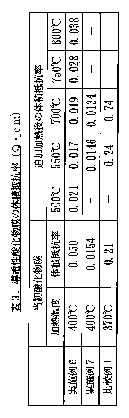
上記で測定した500~800℃追加加熱後の各体積抵抗率を表3に、500℃、550℃、750℃、800℃および850℃追加加熱後の各X線回折チャートを図10に、それぞれ示した。また、500℃追加加熱後に観察した原子間力顕微鏡像を図11に示した。X線チャートの結果および後掲の表3の結果から、本組成物から形成された酸化物膜は800℃まではアモルファス状態が安定に維持され、この温度までは高い導電性を示すものであることが確認された。
実施例7
本実施例では、ランタノイド塩およびルテニウム塩として、それぞれ硝酸塩およびニトロシル硝酸塩を使用した場合に形成される酸化物膜の導電性について調べた。
表面に酸化物膜を有する20mm×20mmのシリコン基板上に、上記調製例9で得た組成物を回転数2,000rpm、25秒間の条件でスピンコートした後、150℃のホットプレート上で6秒および250℃のホットプレート上で1分、順次に加熱した後、さらに400℃で5分間加熱して酸化物膜を得た。このスピンコート、順次加熱および追加加熱のサイクルを合計3回繰り返して膜厚200nmの酸化物膜を得た。ここで得た酸化物膜につき、体積抵抗率の測定を行った。
体積抵抗率測定後の酸化物膜に対し、流速0.2L(STP)/分の酸素気流中でさらに550℃10分間の追加加熱を行った後、体積抵抗率の測定を行った。
この体積抵抗率の測定後の酸化物膜に対し、流速0.2L(STP)/分の酸素気流中でさらに700℃10分間の追加加熱を行った後、再度体積抵抗率を測定した。
上記で測定した各体積抵抗率を表3にそれぞれ示した。
比較例1
本比較例では、ランタノイド塩およびルテニウム塩として、それぞれ塩化物を使用した場合に形成される酸化物膜の導電性について調べた。
表面に酸化物膜を有する20mm×20mmのシリコン基板上に、上記比較調製例1で得た組成物を回転数2,000rpm、25秒間の条件でスピンコートした後、150℃のホットプレート上で6秒および250℃のホットプレート上で1分順次に加熱し、さらに370℃で5分間追加加熱して膜厚70nmの酸化物膜を得た。ここで得た酸化物膜につき、流速0.2L(STP)/分の酸素気流中でさらに550℃10分間の追加加熱を行った後、体積抵抗率の測定を行った。
この体積抵抗率の測定後の酸化物膜に対し、流速0.2L(STP)/分の酸素気流中でさらに700℃、10分間の追加加熱を行った後、再度体積抵抗率を測定した。
上記で測定した各体積抵抗率を表3にそれぞれ示した。
調製例10~12
上記調製例8において、酢酸ランタン1.5水塩の使用量を0.360g(調製例10)、0.420g(調製例11)および0.480g(調製例12)にそれぞれ変更したほかは調製例8と同様にしてLa/Ruのモル比が1.2、1.4および1.6(モル/モル)の組成物をそれぞれ調製した。
<導電性酸化物膜の形成および評価>
実施例8
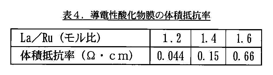
本実施例では、La/Ruのモル比が1.0を超える場合の酸化物導電性膜について調べた。
表面に酸化物膜を有する20mm×20mmのシリコン基板上に、上記調製例10~12で得た組成物のそれぞれを、回転数2,000rpm、25秒間の条件でスピンコートした後、150℃のホットプレート上で6秒、250℃のホットプレート上で1分および400℃のホットプレート上で6秒、順次に加熱した後、さらに450℃で5分間加熱して酸化物膜をそれぞれ得た。このスピンコート、順次加熱および追加加熱のサイクルを合計3回繰り返してそれぞれ膜厚80nm(La/Ru=1.2)、100nm(La/Ru=1.4)、120nm(La/Ru=1.6)の酸化物膜を得た。
これらの酸化物膜に対し、流速0.2L(STP)/分の酸素気流中でさらにそれぞれ550℃30分間の追加加熱を行った。これらの酸化物膜につき、体積抵抗率およびX線回折の測定を行った。
体積抵抗率の測定結果を表4に、X線回折チャートを図12にそれぞれ示した。
実施例9
本実施例では、本発明の導電性酸化物膜形成用組成物を用いるナノインプリント法によって、パターン状の導電性酸化物膜を形成した。
ナノインプリントの実験は、プレス機付きナノインプリント実験装置(試作機)を用いて行った。
このプレス機付きナノインプリント実験装置は、主として台座、モールドホルダおよび2枚のプレス用金属板からなる。2枚のプレス用金属板は、それぞれ加熱装置および温度調節機を備えており、これらに挟持された台座、モールドホルダなどを200℃まで加熱することができる。これら2枚のプレス用金属板は、これらに挟持された台座、モールドホルダなどを、てこの原理によりプレスすることができ、ロードセルによりそのプレス圧力を知ることができる。
[ナノインプリントの実験例]
TEOS加工基板モールド(線幅0.2~10μmの異なる線幅の複数のライン・アンド・スペース・パターンを有するナノインプリント試験用のモールドである。)に、「デュラサーフHD−1100」をスピンコート法により塗布し、次いで60℃にて5分加熱することにより、離型処理を施した。
転写用基板としてシリコンウェハーを用い、このウェハーの表面上に、上記調製例7で得た、La/Ruの比が0.9(モル/モル)であり、キレート剤を含有する組成物を、回転数2,000rpm、回転時間25秒のスピンコートで塗布し、次いで150℃にて6秒間加熱することにより、被膜を形成した。
この被膜を有するシリコンウェハーをプレス機付きナノインプリント実験装置に装着し、被膜上に、TEOS加工基板モールドを圧力5MPaで押し付けた状態で、200℃にて5分間の加熱処理を行った。放冷後、加圧を除去し、加圧および加熱後の被膜を有するシリコンウェハーおよびTEOS加工基板モールドを取り出して、TEOS加工基板モールドを静かに剥離することにより、TEOS加工基板モールドの有するパターンが転写されたパターンを得た。このパターンに対し、流速0.2L(STP)/分の酸素気流中でさらに550℃5分間の追加加熱を行い、パターン状の導電性酸化物膜とした。
上記パターン状の導電性酸化物膜につき、原子間力顕微鏡を用いて観察したところ、良好な転写が確認された。このとき撮影された原子間力顕微鏡写真を、図13に示した。この写真により、線幅0.2μm程度のライン・アンド・スペース・パターンが良好な転写性で形成されていることが確認された。
ここで、追加加熱によっても結晶化に伴うパターンの歪みないし変形が全く見られず、良好な転写性が維持されていることが、本発明の大きな利点の一つである。すなわち、本発明による導電性酸化物膜は、高温の加熱によっても結晶化することなくアモルファス状態が安定に維持されるから、結晶化に伴う歪みや変形が起こることがなく、また結晶サイズに制限されることなく微細なパターンが正確に転写されたパターン状導電性酸化物膜を容易に形成することができる。
さらに本発明によるパターン状導電性酸化物膜は、形成後に加熱されても結晶化することがなく、歪みや変形を生ずることがないから、素子のアニーリングを要する電子デバイスの製造の全工程にわたって形状安定性に優れ、高い導電性が維持される。
<導電性酸化物膜形成用組成物の調製>
調製例13~27
容量13.5mLのガラスびん中に、各酸化物前駆体化合物およびプロピオン酸をそれぞれ表5に示した量だけ仕込んだ。ガラスびんの内容物を室温で撹拌しつつ、ここに、0.75gのモノエタノールアミン(MEA)をゆっくりと滴下した。次いでガラスびんに栓をして、温度を150℃に設定したホットプレート上で、調製例13~25については40分間、調製例26および27については2時間、それぞれ内容物を撹拌しながら加熱して、酸化物前駆体化合物を溶解した。わずかに粘調な溶液が得られた。この溶液を3.25gの1−ブタノールで希釈することにより、金属元素の合計濃度が0.135モル/kgの溶液を得て、これを導電性酸化物膜形成用組成物とした。
表5における酸化物前駆体化合物の略称は、それぞれ以下の意味である。
La−ac:酢酸ランタン1.5水塩(99.99%、関東化学(株)製)、
Ce−ac:酢酸セリウム(III)一水塩(99.99%、関東化学(株)製)、
Pr−ac:酢酸プラセオジム(III)含水塩(99.9%、和光純薬工業(株)製)、
Nd−ac:酢酸ネオジム一水塩(99.9%、和光純薬工業(株)製)、
Sm−ac:酢酸サマリウム四水塩(99.9%、和光純薬工業(株)製)、
Eu−ac:酢酸ユーロピウム(III)含水塩(99.9%、和光純薬工業(株)製)、
Gd−ac:酢酸ガドリニウム(III)含水塩(99.9%、Aldrich製)、
Tb−ac:酢酸テルビウム(III)四水塩(99.9%、和光純薬工業(株)製)、
Dy−ac:酢酸ジスプロシウム四水塩(99.9%、和光純薬工業(株)製)、
Ho−ac:酢酸ホルミウム四水塩(99.9%、和光純薬工業(株)製)、
Er−ac:酢酸エルビウム四水塩(99.9%、和光純薬工業(株)製)、
Tm−ac:酢酸ツリウム四水塩(99.9%、和光純薬工業(株)製)、
Yb−ac:酢酸イッテルビウム(III)四水塩(99.9%、Aldrich製)、
Lu−ac:酢酸ルテチウム四水塩(99.9%、和光純薬工業(株)製)、
および
Ru−noac:ニトロシル酢酸ルテニウム(III)無水塩(99.99%、Alfa Aesar製)
Ir−ac:酢酸イリジウム(III)無水塩(Ir含量=約48%、ChemPur製)、
Rh−ac:酢酸ロジウム無水塩(Rh含量=35~40%、ChemPur製)

実施例10
本実施例では、ランタノイド−ルテニウム酸化物膜において、ランタノイドとして、ランタン以外の金属元素を用いた場合の効果について調べた。
表面に酸化物膜を有する20mm×20mmのシリコン基板上に、上記調製例13~25で得た組成物を、回転数2,000rpm、25秒間の条件でそれぞれスピンコートした後、150℃のホットプレート上で6秒および250℃のホットプレート上で1分、順次に加熱した後、さらに400℃で5分間加熱して膜厚約20nmの酸化物膜を得た。このスピンコート、順次加熱および追加加熱のサイクルを合計3回繰り返して膜厚約60nmの酸化物膜を得た。ここで得た酸化物膜につき、体積抵抗率の測定を行った。
体積抵抗率測定後の酸化物膜に対し、流速0.2L(STP)/分の酸素気流中でさらに500℃10分間の追加加熱を行った後、再度体積抵抗率を測定した。さらに、上記体積抵抗率測定後の酸化物膜に対し、加熱温度および時間を550℃10分および650℃10分として、上記と同様にして順次に追加加熱を行い、各温度における追加加熱後にそれぞれ体積抵抗率を測定した。
650℃追加加熱後の各酸化物膜について、X線回折を測定した。ランタノイドとしてセリウムを用いた実験例については、上記のほか、550℃追加加熱後にもX線回折を測定した。
上記で測定した各体積抵抗率を表6に、650℃追加加熱後のX線回折チャートを図14に、それぞれ示した。また、ランタノイドとしてセリウムを用いた実験例について、550℃追加加熱後および650℃追加加熱後のX線回折チャートを図15に示した。

セリウム以外を用いた場合には、650℃の追加加熱後であっても結晶性は見られず、体積抵抗率も小さいことが分かる。特に、ランタノイドがプラセオジム、ネオジム、サマリウム、ユウロピウムまたはガドリニウムである場合の体積抵抗率が小さい。
実施例11
本実施例では、ランタノイド−ルテニウム酸化物膜において、ルテニウムの代わりにイリジウムまたはロジウムを用いた場合の効果について調べた。
上記調製例26および27で得た組成物をそれぞれ用いたほかは、上記実施例10と同様に、表面に酸化物膜を有するシリコン基板上へ組成物をスピンコートした後、150℃、250℃および400℃における順次の加熱サイクルを3回繰り返して、膜厚約60nmの酸化物膜を得た。ここで得た酸化物膜につき、体積抵抗率の測定を行った。
体積抵抗率測定後の酸化物膜に対し、流速0.2L(STP)/分の酸素気流中でさらに、ランタン−イリジウム酸化物膜については500℃30分、550℃30分、600℃10分および650℃10分の追加加熱を順次に、
ランタン−ロジウム酸化物膜については500℃10分、600℃10分、700℃10分、800℃10分および850℃5分の追加加熱を順次に、それぞれ行った。このとき、温度700℃以下の追加加熱後には、酸化物膜の体積抵抗率を測定した。
また、ランタン−イリジウム酸化物膜については、500℃および650℃における追加加熱後の酸化物膜のX線回折を測定した。ランタン−ロジウム酸化物膜については、追加加熱前(400℃加熱後)および各温度における追加加熱後の酸化物膜のX線回折を測定した。
上記で測定した各体積抵抗率を表7に、ランタン−イリジウム酸化物膜のX線回折チャートを図16に、そしてランタン−ロジウム酸化物膜のX線回折チャートを図17に、それぞれ示した。
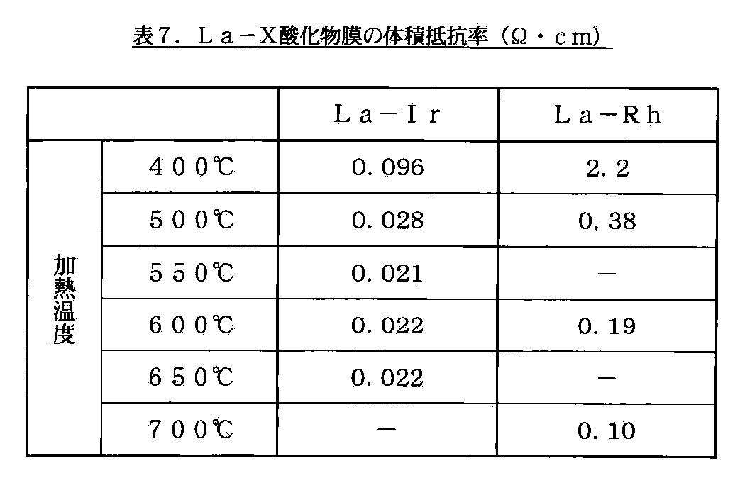
<導電性酸化物膜の半導体性、構成元素比率およびキャリアタイプ>
実施例12
本実施例では、ランタン−ルテニウム酸化物膜が半導体性を有することの確認を行った。
上記調製例8と同様にして調製した組成物(La/Ru比が1.0(モル/モル)であり、La濃度およびRu濃度がそれぞれ0.067モル/kgである組成物)を用い、基板としてクォーツガラス基板上を用いたほかは、実施例6と同様に基板上へ組成物をスピンコートした後、150℃、250℃および400℃における順次の加熱サイクルを5回繰り返して、膜厚約100nmの酸化物膜を得た。次いで、流速0.2L(STP)/分の酸素気流中で500℃10分の追加加熱を行うことにより、加熱温度500℃の酸化物膜を得た。
上記において、追加加熱温度を650℃としたほかは上記と同様に実施することにより、加熱温度650℃の別の酸化物膜を得た。
これら2枚の酸化物膜につき、物理特性測定装置(PPMS、米国のQuantum Design,Inc.製)を用いて比抵抗ρの温度依存性を調べた。得られた比抵抗−温度曲線を図18に示した。
図18を見ると、温度の上昇とともに比抵抗が減少している。このことから、ランタン−ルテニウム酸化物膜は半導体であることが確認された。
実施例13
基板として表面に酸化物膜を有するシリコンウェハを用いたほかは、上記実施例12における加熱温度650℃の酸化物膜と同様に形成して得た膜につき、上記実施例5と同じRBS/HFS/NRAシステムを用いて元素分析を行った。その結果、La/Ru/O/C/H/Clの元素比は、9.9/10.0/37.8/2.7/0.0/0.2(モル比)であった。
La/Ru比としては、ほぼ仕込みどおりの値が得られた。また、形成された膜は、La、RuおよびOのほかに有意量のCを含有していることから、酸化物のほかに有機成分の残滓を含有する新規な組成の導電性膜であることが確認された。微量のClは、使用したLa前駆体またはRu前駆体の不純物に由来すると考えられる。
La/Ru/Oの元素比から、Laは3価であり、Ruは4価であるものと考えられる(理論組成比=LaRuO3.5)。
実施例14
本実施例では、ランタン−ルテニウム酸化物膜中のキャリアタイプを調べた。
追加加熱時間をそれぞれ30分としたほかは上記実施例12と同様にして、加熱温度がそれぞれ500℃および650℃である2枚のランタン−ルテニウム酸化物膜を得た。これらの酸化物膜につき、ホール効果・比抵抗測定装置(品名「ResiTest8300」、(株)東洋テクニカ製)を用いて、室温におけるゼーベック係数を調べた。
ゼーベック係数は、加熱温度500℃のとき+9.05μV/K、加熱温度650℃のとき+7.98μV/Kと、いずれも正の値であり、これらの酸化物膜がp型半導体性を有することが確認された。
実施例15
本実施例では、ランタン−イリジウム酸化物膜中のキャリアタイプを調べた。
上記調製例26と同様にして調製した組成物(La−Ir)を使用して、上記実施例14のうちの追加加熱温度が500℃である場合と同様にして、加熱温度が500℃であるランタン−イリジウム酸化物膜を得た。
この酸化物膜のゼーベック係数を実施例14と同様にして調べたところ、+4.92μV/Kと正の値であり、p型半導体性を有することが確認された。
上記実施例14および15の結果を、表8にまとめた。
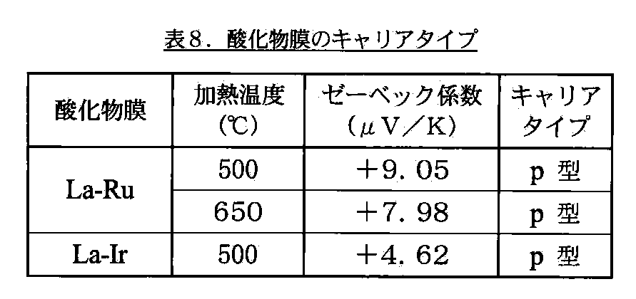
本発明によると、高い導電性を示すとともに、高温に加熱してもアモルファス構造が安定に維持される導電性酸化物膜を、簡易な液相プロセスによって形成するための前駆体組成物および方法が提供される。
本発明の前駆体組成物から形成された導電性酸化物膜は、安定なアモルファス構造を有し、高温に加熱された場合であっても結晶化することがないから、製造工程中に高温加熱を要する電子デバイスに適用しても、結晶サイズの制約のない微細な電極、配線などを容易に形成することができる。
また、本発明の前駆体組成物から形成された導電性酸化物膜は、良好な半導体特性を示し、p型導電性を示す。従って、化合物半導体膜を形成するための他の塗布型の前駆体組成物とともに本発明の前駆体組成物を使用すると、液相プロセスのみの簡易な工程によって実用的な半導体素子を製造することが可能となる。
Claims (10)
- ランタノイド(ただし、セリウムを除く。)のカルボン酸塩、硝酸塩および硫酸塩よりなる群から選択される少なくとも1種と
ルテニウム、イリジウムまたはロジウムのカルボン酸塩、ニトロシルカルボン酸塩、ニトロシル硝酸塩およびニトロシル硫酸塩よりなる群から選択される少なくとも1種と
カルボン酸、アルコールおよびケトンよりなる群から選択される少なくとも1種を含有する溶媒と
を含有することを特徴とする、アモルファス導電性酸化物膜形成用組成物。 - 上記溶媒が非水系溶媒である、請求項1に記載の組成物。
- 組成物中のランタノイドの原子数(NA)とルテニウム、イリジウムまたはロジウムの原子数(NB)との比(NA/NB)が0.6~2.0である、請求項1または2に記載の組成物。
- ランタノイドが、ランタン、プラセオジム、ネオジム、サマリウム、ユウロピウムおよびガドリニウムよりなる群から選択される少なくとも1種である、請求項1または2に記載の組成物。
- 基板上に、請求項1または2のいずれか一項に記載の組成物を塗布して塗膜を形成し、該塗膜を酸化性雰囲気下で加熱する工程を経ることを特徴とする、アモルファス導電性酸化物膜の形成方法。
- 請求項5に記載の方法によって形成されたことを特徴とする、アモルファス導電性酸化物膜。
- p型半導体特性を有する、請求項6に記載のアモルファス導電性酸化物膜。
- 基板上に請求項1または2のいずれか一項に記載の組成物を塗布して塗膜を形成し、
該塗膜上にパターン状モールドを配置して前記基板と前記パターン状モールドとの間に塗膜を挟持し、そして
前記塗膜を酸化性雰囲気下で加熱する工程を経ることを特徴とする、パターン状のアモルファス導電性酸化物膜の形成方法。 - 請求項8に記載の方法によって形成されたことを特徴とする、パターン状のアモルファス導電性酸化物膜。
- p型半導体特性を有する、請求項9に記載のパターン状のアモルファス導電性酸化物膜。
Priority Applications (4)
| Application Number | Priority Date | Filing Date | Title |
|---|---|---|---|
| JP2012524599A JP5549989B2 (ja) | 2010-07-14 | 2011-07-08 | アモルファス導電性酸化物膜を形成するための前駆体組成物および方法 |
| KR1020137000874A KR101397789B1 (ko) | 2010-07-14 | 2011-07-08 | 아몰퍼스 도전성 산화물막을 형성하기 위한 전구체 조성물 및 방법 |
| US13/809,993 US9178022B2 (en) | 2010-07-14 | 2011-07-08 | Precursor composition and method for forming amorphous conductive oxide film |
| CN201180034573.0A CN102971807B (zh) | 2010-07-14 | 2011-07-08 | 用于形成非晶体导电性氧化物膜的前体组合物和方法 |
Applications Claiming Priority (2)
| Application Number | Priority Date | Filing Date | Title |
|---|---|---|---|
| JP2010-159475 | 2010-07-14 | ||
| JP2010159475 | 2010-07-14 |
Publications (1)
| Publication Number | Publication Date |
|---|---|
| WO2012008554A1 true WO2012008554A1 (ja) | 2012-01-19 |
Family
ID=45469549
Family Applications (1)
| Application Number | Title | Priority Date | Filing Date |
|---|---|---|---|
| PCT/JP2011/066165 Ceased WO2012008554A1 (ja) | 2010-07-14 | 2011-07-08 | アモルファス導電性酸化物膜を形成するための前駆体組成物および方法 |
Country Status (6)
| Country | Link |
|---|---|
| US (1) | US9178022B2 (ja) |
| JP (1) | JP5549989B2 (ja) |
| KR (1) | KR101397789B1 (ja) |
| CN (1) | CN102971807B (ja) |
| TW (1) | TWI480341B (ja) |
| WO (1) | WO2012008554A1 (ja) |
Cited By (3)
| Publication number | Priority date | Publication date | Assignee | Title |
|---|---|---|---|---|
| WO2013129701A1 (ja) * | 2012-03-02 | 2013-09-06 | 独立行政法人科学技術振興機構 | 導電性膜の形成方法 |
| JPWO2013073711A1 (ja) * | 2011-11-18 | 2015-04-02 | 独立行政法人科学技術振興機構 | アモルファス導電性酸化物膜の形成方法 |
| JP2015513210A (ja) * | 2012-01-27 | 2015-04-30 | メルク パテント ゲゼルシャフト ミット ベシュレンクテル ハフツングMerck Patent Gesellschaft mit beschraenkter Haftung | 改善された伝導率を持つ、電気的に半導体性または伝導性の金属酸化物層の生産のための方法 |
Families Citing this family (1)
| Publication number | Priority date | Publication date | Assignee | Title |
|---|---|---|---|---|
| EP4117042A1 (en) * | 2021-07-03 | 2023-01-11 | Imec VZW | Mixed metal oxide |
Citations (4)
| Publication number | Priority date | Publication date | Assignee | Title |
|---|---|---|---|---|
| JPH082928A (ja) * | 1994-05-31 | 1996-01-09 | Rohm & Haas Co | 無機含有複合材料 |
| JP2002047011A (ja) * | 2000-08-02 | 2002-02-12 | Mitsubishi Materials Corp | 緻密質ペロブスカイト型金属酸化物薄膜の形成方法及び緻密質ペロブスカイト型金属酸化物薄膜 |
| JP2002321923A (ja) * | 2001-02-20 | 2002-11-08 | National Institute For Materials Science | ルテニウムペロブスカイトの製造方法 |
| JP2010013514A (ja) * | 2008-07-02 | 2010-01-21 | Fujifilm Corp | ナノインプリント用硬化性組成物、これを用いた硬化物、並びに、液晶表示装置用部材 |
Family Cites Families (11)
| Publication number | Priority date | Publication date | Assignee | Title |
|---|---|---|---|---|
| US6541375B1 (en) * | 1998-06-30 | 2003-04-01 | Matsushita Electric Industrial Co., Ltd. | DC sputtering process for making smooth electrodes and thin film ferroelectric capacitors having improved memory retention |
| JP3557920B2 (ja) * | 1998-10-20 | 2004-08-25 | 三菱マテリアル株式会社 | 酸化物薄膜形成用溶液 |
| JP2000143251A (ja) * | 1998-11-06 | 2000-05-23 | Mitsubishi Materials Corp | 酸化物薄膜形成用溶液 |
| JP2000348549A (ja) * | 1999-06-04 | 2000-12-15 | Mitsubishi Materials Corp | Sro導電性薄膜形成用組成物及びsro導電性薄膜の形成方法 |
| DE60233180D1 (de) * | 2001-02-20 | 2009-09-17 | Nat Inst For Materials Science | Verfahren zur Herstellung von Rutheniumperovskit |
| JP2003277966A (ja) * | 2002-03-22 | 2003-10-02 | Asahi Kasei Corp | 低い過電圧と耐久性に優れた水素発生用陰極 |
| WO2004068235A1 (ja) * | 2003-01-27 | 2004-08-12 | Fujitsu Limited | 光偏向素子およびその製造方法 |
| KR100609699B1 (ko) * | 2004-07-15 | 2006-08-08 | 한국전자통신연구원 | 급격한 금속-절연체 전이 반도체 물질을 이용한 2단자반도체 소자 및 그 제조 방법 |
| JP4274489B2 (ja) * | 2006-10-25 | 2009-06-10 | クロリンエンジニアズ株式会社 | 水素発生用電極およびその製造方法 |
| KR100974288B1 (ko) * | 2010-01-13 | 2010-08-05 | 한국기계연구원 | 나노임프린트를 이용한 금속 산화박막 패턴 형성방법 및 이를 이용한 led 소자의 제조방법 |
| JP5327977B2 (ja) | 2010-04-21 | 2013-10-30 | 独立行政法人科学技術振興機構 | 導電性膜形成用組成物および導電性膜の形成方法 |
-
2011
- 2011-07-08 KR KR1020137000874A patent/KR101397789B1/ko not_active Expired - Fee Related
- 2011-07-08 JP JP2012524599A patent/JP5549989B2/ja not_active Expired - Fee Related
- 2011-07-08 WO PCT/JP2011/066165 patent/WO2012008554A1/ja not_active Ceased
- 2011-07-08 US US13/809,993 patent/US9178022B2/en not_active Expired - Fee Related
- 2011-07-08 CN CN201180034573.0A patent/CN102971807B/zh not_active Expired - Fee Related
- 2011-07-13 TW TW100124788A patent/TWI480341B/zh not_active IP Right Cessation
Patent Citations (4)
| Publication number | Priority date | Publication date | Assignee | Title |
|---|---|---|---|---|
| JPH082928A (ja) * | 1994-05-31 | 1996-01-09 | Rohm & Haas Co | 無機含有複合材料 |
| JP2002047011A (ja) * | 2000-08-02 | 2002-02-12 | Mitsubishi Materials Corp | 緻密質ペロブスカイト型金属酸化物薄膜の形成方法及び緻密質ペロブスカイト型金属酸化物薄膜 |
| JP2002321923A (ja) * | 2001-02-20 | 2002-11-08 | National Institute For Materials Science | ルテニウムペロブスカイトの製造方法 |
| JP2010013514A (ja) * | 2008-07-02 | 2010-01-21 | Fujifilm Corp | ナノインプリント用硬化性組成物、これを用いた硬化物、並びに、液晶表示装置用部材 |
Cited By (7)
| Publication number | Priority date | Publication date | Assignee | Title |
|---|---|---|---|---|
| JPWO2013073711A1 (ja) * | 2011-11-18 | 2015-04-02 | 独立行政法人科学技術振興機構 | アモルファス導電性酸化物膜の形成方法 |
| JP2015513210A (ja) * | 2012-01-27 | 2015-04-30 | メルク パテント ゲゼルシャフト ミット ベシュレンクテル ハフツングMerck Patent Gesellschaft mit beschraenkter Haftung | 改善された伝導率を持つ、電気的に半導体性または伝導性の金属酸化物層の生産のための方法 |
| WO2013129701A1 (ja) * | 2012-03-02 | 2013-09-06 | 独立行政法人科学技術振興機構 | 導電性膜の形成方法 |
| CN104160456A (zh) * | 2012-03-02 | 2014-11-19 | 独立行政法人科学技术振兴机构 | 导电性膜的形成方法 |
| US9082618B2 (en) | 2012-03-02 | 2015-07-14 | Japan Science And Technology Agency | Method of forming a conductive film |
| JPWO2013129701A1 (ja) * | 2012-03-02 | 2015-07-30 | 独立行政法人科学技術振興機構 | 導電性膜の形成方法 |
| CN104160456B (zh) * | 2012-03-02 | 2016-10-26 | 独立行政法人科学技术振兴机构 | 导电性膜的形成方法 |
Also Published As
| Publication number | Publication date |
|---|---|
| CN102971807A (zh) | 2013-03-13 |
| JP5549989B2 (ja) | 2014-07-16 |
| CN102971807B (zh) | 2016-11-09 |
| KR20130076858A (ko) | 2013-07-08 |
| JPWO2012008554A1 (ja) | 2013-09-09 |
| US20130112973A1 (en) | 2013-05-09 |
| KR101397789B1 (ko) | 2014-05-20 |
| US9178022B2 (en) | 2015-11-03 |
| TW201224068A (en) | 2012-06-16 |
| TWI480341B (zh) | 2015-04-11 |
Similar Documents
| Publication | Publication Date | Title |
|---|---|---|
| TWI425689B (zh) | 導電體物件之製造方法 | |
| TW201041835A (en) | Indium alkoxide-containing compositions, process for preparation thereof and use thereof | |
| US9340678B2 (en) | Process to form aqueous precursor and aluminum oxide film | |
| JP5549989B2 (ja) | アモルファス導電性酸化物膜を形成するための前駆体組成物および方法 | |
| Winkler et al. | Influence of the aqueous solution composition on the morphology of Zn1− x Mg x O films deposited by spray pyrolysis | |
| JP5327977B2 (ja) | 導電性膜形成用組成物および導電性膜の形成方法 | |
| Sunde et al. | Optimisation of chemical solution deposition of indium tin oxide thin films | |
| US9082618B2 (en) | Method of forming a conductive film | |
| US9812330B2 (en) | Formulations for producing indium oxide-containing layers, process for producing them and their use | |
| CN108028270B (zh) | 用于形成n-型氧化物半导体膜的涂布液、n-型氧化物半导体膜制造方法和场效应晶体管制造方法 | |
| JP5863126B2 (ja) | アモルファス導電性酸化物膜の形成方法 | |
| JP5894393B2 (ja) | 酸化物粒子分散液 | |
| KR101640728B1 (ko) | LaNiO3 박막 형성용 조성물 및 이 조성물을 사용한 LaNiO3 박막의 형성 방법 | |
| TWI673327B (zh) | 用於形成金屬氧化物膜的塗佈液、氧化物膜、場效電晶體、及其製造方法 | |
| Todorovska et al. | Spray-pyrolysis deposition of LaMnO3 and La1− xCaxMnO3 thin films | |
| WO2018174218A1 (en) | Coating liquid for forming metal oxide film, oxide film, field-effect transistor, and method for producing the same | |
| TW201500291A (zh) | LaNiO薄膜形成用組成物及使用該組成物之LaNiO薄膜的形成方法 |
Legal Events
| Date | Code | Title | Description |
|---|---|---|---|
| WWE | Wipo information: entry into national phase |
Ref document number: 201180034573.0 Country of ref document: CN |
|
| 121 | Ep: the epo has been informed by wipo that ep was designated in this application |
Ref document number: 11806884 Country of ref document: EP Kind code of ref document: A1 |
|
| WWE | Wipo information: entry into national phase |
Ref document number: 2012524599 Country of ref document: JP |
|
| ENP | Entry into the national phase |
Ref document number: 20137000874 Country of ref document: KR Kind code of ref document: A |
|
| NENP | Non-entry into the national phase |
Ref country code: DE |
|
| WWE | Wipo information: entry into national phase |
Ref document number: 13809993 Country of ref document: US |
|
| 122 | Ep: pct application non-entry in european phase |
Ref document number: 11806884 Country of ref document: EP Kind code of ref document: A1 |