WO2012008541A1 - コンタクトプローブおよびプローブユニット - Google Patents
コンタクトプローブおよびプローブユニット Download PDFInfo
- Publication number
- WO2012008541A1 WO2012008541A1 PCT/JP2011/066141 JP2011066141W WO2012008541A1 WO 2012008541 A1 WO2012008541 A1 WO 2012008541A1 JP 2011066141 W JP2011066141 W JP 2011066141W WO 2012008541 A1 WO2012008541 A1 WO 2012008541A1
- Authority
- WO
- WIPO (PCT)
- Prior art keywords
- contact
- probe
- elastic
- contact probe
- contact portion
- Prior art date
- Legal status (The legal status is an assumption and is not a legal conclusion. Google has not performed a legal analysis and makes no representation as to the accuracy of the status listed.)
- Ceased
Links
Images






Classifications
-
- H—ELECTRICITY
- H01—ELECTRIC ELEMENTS
- H01R—ELECTRICALLY-CONDUCTIVE CONNECTIONS; STRUCTURAL ASSOCIATIONS OF A PLURALITY OF MUTUALLY-INSULATED ELECTRICAL CONNECTING ELEMENTS; COUPLING DEVICES; CURRENT COLLECTORS
- H01R13/00—Details of coupling devices of the kinds covered by groups H01R12/70 or H01R24/00 - H01R33/00
- H01R13/02—Contact members
- H01R13/22—Contacts for co-operating by abutting
- H01R13/24—Contacts for co-operating by abutting resilient; resiliently-mounted
- H01R13/2442—Contacts for co-operating by abutting resilient; resiliently-mounted with a single cantilevered beam
-
- G—PHYSICS
- G01—MEASURING; TESTING
- G01R—MEASURING ELECTRIC VARIABLES; MEASURING MAGNETIC VARIABLES
- G01R1/00—Details of instruments or arrangements of the types included in groups G01R5/00 - G01R13/00 and G01R31/00
- G01R1/02—General constructional details
- G01R1/04—Housings; Supporting members; Arrangements of terminals
- G01R1/0408—Test fixtures or contact fields; Connectors or connecting adaptors; Test clips; Test sockets
- G01R1/0433—Sockets for IC's or transistors
- G01R1/0441—Details
- G01R1/0466—Details concerning contact pieces or mechanical details, e.g. hinges or cams; Shielding
-
- H—ELECTRICITY
- H01—ELECTRIC ELEMENTS
- H01R—ELECTRICALLY-CONDUCTIVE CONNECTIONS; STRUCTURAL ASSOCIATIONS OF A PLURALITY OF MUTUALLY-INSULATED ELECTRICAL CONNECTING ELEMENTS; COUPLING DEVICES; CURRENT COLLECTORS
- H01R12/00—Structural associations of a plurality of mutually-insulated electrical connecting elements, specially adapted for printed circuits, e.g. printed circuit boards [PCB], flat or ribbon cables, or like generally planar structures, e.g. terminal strips, terminal blocks; Coupling devices specially adapted for printed circuits, flat or ribbon cables, or like generally planar structures; Terminals specially adapted for contact with, or insertion into, printed circuits, flat or ribbon cables, or like generally planar structures
- H01R12/70—Coupling devices
- H01R12/7076—Coupling devices for connection between PCB and component, e.g. display
-
- H—ELECTRICITY
- H01—ELECTRIC ELEMENTS
- H01R—ELECTRICALLY-CONDUCTIVE CONNECTIONS; STRUCTURAL ASSOCIATIONS OF A PLURALITY OF MUTUALLY-INSULATED ELECTRICAL CONNECTING ELEMENTS; COUPLING DEVICES; CURRENT COLLECTORS
- H01R13/00—Details of coupling devices of the kinds covered by groups H01R12/70 or H01R24/00 - H01R33/00
- H01R13/02—Contact members
- H01R13/22—Contacts for co-operating by abutting
- H01R13/24—Contacts for co-operating by abutting resilient; resiliently-mounted
- H01R13/2435—Contacts for co-operating by abutting resilient; resiliently-mounted with opposite contact points, e.g. C beam
-
- H—ELECTRICITY
- H01—ELECTRIC ELEMENTS
- H01R—ELECTRICALLY-CONDUCTIVE CONNECTIONS; STRUCTURAL ASSOCIATIONS OF A PLURALITY OF MUTUALLY-INSULATED ELECTRICAL CONNECTING ELEMENTS; COUPLING DEVICES; CURRENT COLLECTORS
- H01R13/00—Details of coupling devices of the kinds covered by groups H01R12/70 or H01R24/00 - H01R33/00
- H01R13/40—Securing contact members in or to a base or case; Insulating of contact members
- H01R13/405—Securing in non-demountable manner, e.g. moulding, riveting
-
- H—ELECTRICITY
- H01—ELECTRIC ELEMENTS
- H01R—ELECTRICALLY-CONDUCTIVE CONNECTIONS; STRUCTURAL ASSOCIATIONS OF A PLURALITY OF MUTUALLY-INSULATED ELECTRICAL CONNECTING ELEMENTS; COUPLING DEVICES; CURRENT COLLECTORS
- H01R2201/00—Connectors or connections adapted for particular applications
- H01R2201/20—Connectors or connections adapted for particular applications for testing or measuring purposes
Definitions
- the present invention relates to a contact probe and a probe unit used for connection between electric circuit boards and the like.
- an electrical connection is made between the inspection target and a signal processing device that outputs an inspection signal.
- a probe unit that accommodates a plurality of conductive contact probes is used.
- the probe unit can be applied to highly integrated and miniaturized inspection objects by narrowing the pitch between contact probes with the progress of high integration and miniaturization of semiconductor integrated circuits and liquid crystal panels in recent years. Possible technologies are progressing.
- Wire-type contact probes are easier to reduce in diameter than pin-type contact probes that use springs.
- adjacent contact probes contact each other. Or the contact with the contacted object may vary. For this reason, in the wire-type contact probe, various devices are provided to uniformly align the direction of bending due to the load.
- Patent Document 1 an elastomer made of rubber or resin is provided for the contact probe, and the elastomer is elastically deformed by the contact between the contact probe and the electrode, so that the contact state between the contact probe and the electrode is maintained. is doing.
- Patent Document 2 discloses a probe unit in which a plurality of contact probes having a spring shape and curved in contact with a contact body are accommodated in a test board. In this contact probe, a portion having a spring property and a conducting portion of an electric signal are common.
- the evaluation criteria for the conduction state inspection and the operation characteristic inspection of inspection objects are becoming stricter year by year.
- the use environment temperature at the time of performing these inspections is in a wide range of ⁇ 40 to 200 ° C., and durability at these temperatures is also demanded on the inspection apparatus side including the contact probe.
- the present invention has been made in view of the above, and is a contact probe that has a spring property, can obtain reliable and good conduction between contact objects, and can improve durability in a high temperature region. And it aims at providing a probe unit.
- a contact probe is a plate-like contact probe that connects different substrates, and includes a first contact portion that contacts one substrate, and the other A second contact portion that contacts the substrate, a connection portion that connects the first contact portion and the second contact portion, a conduction portion that conducts electrical conductivity between different substrates, and an operating environment temperature of the contact probe.
- An elastic part that is formed using a metal material having a maximum use temperature equal to or higher than the maximum value, extends from the second contact part, and elastically deforms by a load applied to the first contact part and the second contact part,
- the conducting part includes a conductive material different from the metal material.
- the conductive material is a metal or alloy having a higher electrical conductivity than the metal material.
- the contact probe according to the present invention is characterized in that, in the above-described invention, the conductive portion is formed by laminating the conductive material and the metal material that are plate-shaped with each other in the thickness direction.
- the contact probe according to the present invention is characterized in that, in the above-mentioned invention, the elastic portion is formed by laminating the metal material and the conductive material which are plate-shaped with each other in the thickness direction.
- the first and second contact portions are characterized in that the conductive material protrudes to the outer edge side of the metal material.
- the contact probe according to the present invention is characterized in that, in the above invention, the width of the elastic portion is smaller than the width of the connection portion.
- the contact probe according to the present invention is characterized in that, in the above invention, the metal material is a heat-resistant steel, a superalloy, or an electroformed material.
- the elastic portion includes a first plane in contact with the first contact portion, a parallel to the first plane, and the second contact portion. It is located between the 2nd planes which touch.
- the contact probe according to the present invention is characterized in that, in the above invention, a part of the elastic portion is linear.
- a probe unit according to the present invention includes the contact probe according to the above-described invention and a holding portion that holds the contact probe.
- the contact probe and the probe unit according to the present invention each have a portion having conductivity and a portion having spring property at different positions of the contact probe, and the portion having conductivity is a heat-resistant steel, a superalloy, an electroformed material, or the like. Since the conductive material is different from the portion having the spring property formed by using the metal material, it has the spring property, and reliable and good conduction can be obtained between the contact objects, and the high temperature region. The effect that the durability with respect to can be improved is produced.
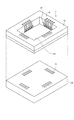
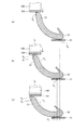
- FIG. 1 is a perspective view showing the configuration of the probe unit according to the first embodiment of the present invention.
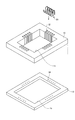
- FIG. 2 is an exploded perspective view showing a configuration of a main part of the probe unit shown in FIG.
- FIG. 3 is an exploded perspective view showing a configuration of a main part of the probe unit shown in FIG.
- FIG. 4 is a perspective view showing a configuration of a main part of the probe unit shown in FIG.
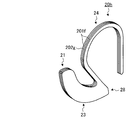
- FIG. 5 is a perspective view showing the contact probe according to the first embodiment of the present invention.
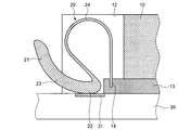
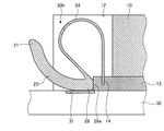
- FIG. 6 is a partial cross-sectional view showing a configuration of a main part of the probe unit shown in FIG.
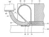
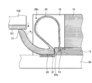
- FIG. 7 is a partial cross-sectional view showing a configuration of a main part of the probe unit shown in FIG. FIG.
- FIG. 8 is a partial cross-sectional view showing a configuration of a main part of the probe unit shown in FIG.
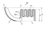
- FIG. 9 is a side view showing a contact probe which is a first modification of the first embodiment of the present invention.
- FIG. 10 is a perspective view showing a contact probe which is a second modification of the first embodiment of the present invention.
- FIG. 11 is a perspective view showing a contact probe which is a third modification of the first embodiment of the present invention.
- FIG. 12 is a perspective view showing a contact probe that is a fourth modification of the first embodiment of the present invention.
- FIG. 13 is a perspective view showing a contact probe which is a fifth modification of the first embodiment of the present invention.
- FIG. 9 is a side view showing a contact probe which is a first modification of the first embodiment of the present invention.
- FIG. 10 is a perspective view showing a contact probe which is a second modification of the first embodiment of the present invention.
- FIG. 11 is a perspective view showing a contact probe
- FIG. 14 is a perspective view showing a contact probe that is a sixth modification of the first embodiment of the present invention.
- FIG. 15 is a perspective view showing a contact probe which is a seventh modification of the first embodiment of the present invention.
- FIG. 16 is a perspective view showing a contact probe according to the second embodiment of the present invention.
- FIG. 17 is a partial cross-sectional view showing the configuration of the main part of the probe unit according to the second embodiment of the present invention.
- FIG. 18 is a partial cross-sectional view showing the configuration of the main part of the probe unit according to the second embodiment of the present invention.
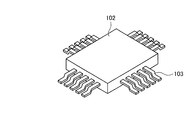
- FIG. 19 is a perspective view showing a semiconductor integrated circuit which is a modification of the embodiment of the present invention.
- FIG. 1 is a perspective view showing the configuration of the probe unit according to the first embodiment of the present invention.
- a probe unit 1 shown in FIG. 1 is a device that is used when an electrical characteristic test is performed on a semiconductor integrated circuit 100 that is an object to be tested, and a circuit that outputs a test signal to the semiconductor integrated circuit 100 and the semiconductor integrated circuit 100.
- This is an apparatus for electrically connecting the substrate 30.
- the semiconductor integrated circuit 100 is described as being a QFN (Quad Flat Non-Leaded Package) having the electrode 101.
- the probe unit 1 includes a conductive contact probe 20 (hereinafter simply referred to as a “probe 20”) that contacts two different objects to be contacted (substrates), that is, a semiconductor integrated circuit 100 and a circuit board 30, and a plurality of probes 20. It has a probe holder 10 as a holding part that receives and holds it in accordance with a predetermined pattern, and a circuit board 30 that abuts on the bottom of the probe holder 10 and outputs a test signal to the semiconductor integrated circuit 100 via the probe 20. .
- a conductive contact probe 20 hereinafter simply referred to as a “probe 20”
- probe 20 that contacts two different objects to be contacted (substrates), that is, a semiconductor integrated circuit 100 and a circuit board 30, and a plurality of probes 20. It has a probe holder 10 as a holding part that receives and holds it in accordance with a predetermined pattern, and a circuit board 30 that abuts on the bottom of the probe holder 10 and output
- the circuit board 30 has an electrode 31 for outputting a test signal to the semiconductor integrated circuit 100 via the probe 20 as shown in FIG.
- the electrode 31 is disposed on the circuit board 30 corresponding to the probe 20 held by the probe holder 10.
- the probe holder 10 and the circuit board 30 may be connected by screws or the like, or may be bonded by an adhesive or a seal member. Any bonding form is possible as long as the contact between the probe 20 and the electrode 31 is not hindered.
- the probe holder 10 is formed using an insulating material, and includes a housing portion 11 in which a housing space capable of housing the semiconductor integrated circuit 100 is formed, and a slit 12 for holding the probe 20 in a predetermined pattern.
- the slit 12 holds the probe 20 so that the tip of the probe 20 protrudes toward the accommodating portion 11 side. Further, when the semiconductor integrated circuit 100 is accommodated in the accommodating portion 11, the slit 12 is formed at a position where each probe 20 contacts the electrode 101 of the corresponding semiconductor integrated circuit 100.
- FIG. 3 is an exploded perspective view showing a configuration of a main part of the probe unit 1 shown in FIG.
- FIG. 4 is a perspective view showing a configuration of a main part of the probe unit 1 shown in FIG.
- the probe holder 10 is configured by detachably connecting a fixing member 13 that fixes the probe 20 to the outer periphery of the bottom.
- the fixing member 13 is formed using an insulating material and has an opening 15 that is larger than the probe holder 10 and a hole 14 that holds and fixes the probe 20.
- the probe holder 10 has a rectangular parallelepiped shape by fitting with the fixing member 13 at a notch corresponding to the fixing member 13 and constitutes a holding portion that holds the probe 20.
- the hole portion 14 accommodates the end portion of the probe 20 inserted through the slit 12, and holds the probe 20 so that the other tip portion of the probe 20 is positioned at a predetermined position of the accommodation portion 11. If the probe 20 can be fixed at a predetermined interval and in a predetermined direction, the holding portion may be configured only by the fixing member 13, and the probe unit 10 and the hole portion 14 of the fixing member 13 are integrally formed. Also good.
- FIG. 5 is a perspective view showing the probe 20 according to the first embodiment of the present invention.
- 6 is a cross-sectional view taken along a plane passing through the center of the slit 12 shown in FIG.
- the probe 20 shown in FIGS. 5 and 6 is formed by laminating a metal plate 201 and a metal plate 202 having a substantially flat plate shape with a uniform plate thickness in the thickness direction, and has a side surface that forms an arc shape at the tip.
- the first contact portion 21 that contacts the semiconductor integrated circuit 100 at the side surface
- the second contact portion 22 that has an arc-shaped side surface and contacts the circuit board 30 at the side surface, the first contact portion 21 and the second contact portion.
- the elastic part which extends from the 2nd contact part 22, the part which comprises arc shape, and is elastically deformed with the load added to the 1st contact part 21 and the 2nd contact part 22 has the strip
- the arc-shaped side surface of the second contact portion 22 is held by the probe holder 10 and comes into contact with the electrode 31 of the circuit board 30 as shown in the cross-sectional view of FIG.
- the elastic part 24 has a smaller width than the width of the connection part 23. For this reason, the elastic portion 24 is more likely to be elastically deformed than the other portions with respect to the load applied to the first contact portion 21 or the second contact portion 22.
- the ratio between the width of the elastic part 24 and the width of the connecting part 23 may be any ratio as long as the elastic part 24 can be preferentially elastically deformed.
- the end portion of the elastic portion 24 in a direction different from the second contact portion 22 extends in a straight line shape, and the tip end portion of the straight line portion is inserted into the hole portion 14 so that the probe 20 is attached to the probe portion. It is held by the holder 10.
- Examples of the metal material forming the metal plate 201 include heat-resistant steel, superalloy, or electroformed material having a maximum use temperature of 200 ° C. or more when the maximum value of the use environment temperature is about 200 ° C.
- Examples of the heat resistant steel include austenitic stainless steel, alloy tool steel, precipitation hardening stainless steel, and the like.
- Examples of the superalloy include a nickel base superalloy, a cobalt base superalloy, and a nickel-cobalt superalloy, which are alloys mainly composed of nickel base and cobalt base.
- a metal having a melting point of 600 ° C. or more can be used.
- An example of such a metal is a nickel-based electroformed material.
- the maximum use temperature is an amount obtained from the linear shrinkage ratio with respect to heating, and is an amount indicating the heat resistance characteristics of the material.
- Examples of the metal forming the metal plate 202 include a conductive material such as a metal or an alloy having an electric resistivity of 1.0 ⁇ 10 ⁇ 7 ⁇ ⁇ m or less.
- Examples of the metal include gold, copper, nickel, silver, platinum, and rhodium. Note that any metal or alloy having higher electrical conductivity than the metal material forming the metal plate 201 is applicable.
- the metal plate 201 suppresses the deformation of the probe 20 due to the elastic deformation of the elastic portion 24 being maintained in a high temperature state, and the metal plate 202 reliably Good electrical conduction can be performed.
- FIG. 7 is a partial cross-sectional view showing a state in which a load is applied to the first contact portion 21 or the second contact portion 22.
- FIG. 7 when the first contact portion 21 contacts the electrode 101 of the semiconductor integrated circuit 100 and a load is applied in the direction of the arrow in the figure, the curved portion of the elastic portion 24 is elastically deformed.
- broken lines P 0 indicates the position of the probe 20 in a state where no load is applied as shown in FIG.
- the first contact portion 21 and the second contact portion 22 are not elastically deformed and contact the electrodes 101 and 31 according to the load. Move while touching. Further, the elastic portion 24 undergoes elastic deformation in accordance with a load transmitted via the connection portion 23 and the second contact portion 22. In addition, the conduction
- FIG. 8 shows a contact state between the first contact portion 21 and the electrode 101 and a contact state between the second contact portion 22 and the electrode 31 when a load is applied to the first contact portion 21 and the elastic portion 24 is elastically deformed.
- FIG. 8A shows a state where the electrode 101 of the semiconductor integrated circuit 100 is in contact with the first contact portion 21 (a state where no load is applied). In this case, the contact point between the first contact portion 21 and the electrode 101 is S 0 , and the contact point between the second contact portion 22 and the electrode 31 is C 0 .
- FIG. 8A when the semiconductor integrated circuit 100 moves in the direction of the arrow, a load is applied to the first contact portion 21 and the first contact portion 21 is pushed down. Due to the movement of the first contact portion 21, the contact points of the first contact portion 21 and the second contact portion 22 with the electrodes 101 and 31 are shifted to S 1 and C 1 respectively (FIG. 8B).
- the broken line P 0 indicates the position of the probe 20 in a state where no load is applied as shown in FIG. 8A, and the broken line I 0 indicates the position of the semiconductor integrated circuit 100 shown in FIG. Yes.
- each contact part 21 and the second contact portion 22 rotate on the electrodes 101 and 31, and the contact points move. For this reason, each contact part has a small frictional force applied to each electrode, and can suppress wear of the contact part and each electrode.
- the probe unit 1 In the probe unit 1 according to the first embodiment described above, different metals are laminated, and the portion that conducts electricity in the same probe and the portion having spring properties are made different from each other.
- the probe can be designed without a long conduction path, ensuring reliable electrical continuity, and preventing deformation of the probe due to repeated use at high temperatures or prolonged pressurization. It becomes.
- each contact part rotates with respect to a contact with an electrode and moves a contact, the friction between a contact part and an electrode can be reduced and abrasion of a contact part and an electrode can be suppressed.
- the stacked relationship between the metal plate 201 and the metal plate 202 may be reversed, or a configuration in which one metal plate 201 and the metal plate 202 are bonded together may be used. And the structure by which the some metal plate of four or more layers is laminated
- stacked may be sufficient.
- the probe according to the first embodiment described above has a configuration in which the elastic plate 24 side is formed of the metal plate 201 and the conductive portion is formed of the metal plate 202, and then the metal plate 201 and the metal plate 202 are connected. May be.
- FIG. 9 is a plan view showing a probe 20a which is a first modification of the first embodiment.
- the metal plate 202 that conducts electrical continuity between the first contact portion 21a and the second contact portion 22a is obtained from the metal plate 201.
- FIG. 10 is a perspective view showing a probe 20b that is a second modification of the first embodiment.
- a metal plate 202a formed of the above-described material for forming the metal plate 202 is laminated on a portion corresponding to the conductive portion with respect to the metal plate 201 having the above-described shape.
- FIG. 11 is a perspective view showing a probe 20c, which is a third modification of the first embodiment.
- the elastic portion 25 is formed to be curved so that the straight portions on both ends are parallel. Further, the radius of curvature of the curved portion of the elastic portion 25 is smaller than the radius of curvature of the elastic portion 24 shown in FIG. Note that the width of the elastic portion 25 is smaller than the width of the connecting portion 23.
- the probe 20c described above is effective when the device is downsized because the curved portion of the elastic portion 25 is small. Further, when the contact direction of the probe 20 and the semiconductor integrated circuit 100 is the direction as shown in FIGS. 7 and 8, the formation region of the curved portion of the elastic portion 25 with respect to the moving direction of the semiconductor integrated circuit 100 is the connection portion. Since it does not overlap with the formation region of 23, the probe can be further miniaturized by shortening the connecting portion 23.
- FIG. 12 is a perspective view showing a probe 20d that is a fourth modification of the first embodiment.
- the probe 20d is formed by laminating a metal plate 201b and a metal plate 202c corresponding to the metal plate 201 and the metal plate 202, respectively, and the first contact portion 21 and the second contact described above.
- an elastic portion 24 that is elastically deformed by a load applied to the first contact portion 21c and the second contact portion 22c.
- the probe 20d has the same effect as that of the first embodiment described above, and the radius of curvature of the contact portion with the electrode of the second contact portion 22c is small, and the distance to rotate on the electrode is shortened. Useful when the size is small. Further, since the connection portion 26 has a shorter conduction distance than the arc-shaped connection portion 23 described above, it is possible to obtain more stable conduction.
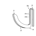
- FIG. 13 is a perspective view showing a probe 20e that is a fifth modification of the first embodiment.
- the probe 20e is formed by laminating a metal plate 201c and a metal plate 202d corresponding to the metal plate 201 and the metal plate 202, respectively, and the first contact portion 21 and the second contact described above.
- an elastic portion 27 that is elastically deformed by a load applied to. Note that the width of the elastic portion 27 is smaller than the width of the connecting portion 23. Moreover, the edge part of the direction different from the 2nd contact part 22 of the elastic part 27 is extended linearly.
- the elastic portion 27 is positioned between the first plane G 1 that is in contact with the first contact portion 21 and the second plane G 2 that is parallel to the first plane G 1 and is in contact with the second contact portion 22. To do. That is, the elastic portion 27, the second plane G 2, the distance d2 to the farthest point in the second plane G 2 of the elastic portion 27, the first plane G 1 and the second plane G 2 It is curved and formed to be smaller than the distance d1 between them.
- the probe 20e has the same effect as that of the first embodiment described above. For example, when the probe 20e is held by the probe holder 1 to perform an inspection, the semiconductor integrated circuit 100 from above in a region including the region where the elastic portion 27 is formed. Even when the two approaches, the elastic part 27 and the semiconductor integrated circuit 100 can be inspected without contact.
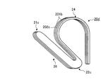
- a probe 20f having an elastic portion 27a having a shape that extends in a zigzag shape by repeating curved portions having opposite concavities and convexities may be used.
- the probe 20f is formed by laminating a metal plate 201d and a metal plate 202e corresponding to the metal plate 201 and the metal plate 202, respectively.
- Elastic portion 27a is reciprocally in a direction substantially orthogonal to the plane G 1, G 2, a shape extending in a direction parallel to the plane G 1, G 2.
- the second plane G 2 the distance d3 to the second point farthest to the plane G 2 of the resilient portion 27a, the distance between the first plane G 1 and the second plane G 2 It is curved and formed so as to be smaller than d1.
- a probe 20g having an elastic portion 27b having a shape that extends in a zigzag shape by repeating curved portions having opposite concavities and convexities may be used.
- the probe 20g is formed by laminating a metal plate 201e and a metal plate 202f corresponding to the metal plate 201 and the metal plate 202, respectively.
- Elastic portion 27b is to reciprocate in a direction parallel to the plane G 1, G 2, a shape extending in the plane G 1, G 2 and perpendicular.
- the second plane G 2 the distance d4 to the second point farthest to the plane G 2 of the elastic portion 27b, the distance between the first plane G 1 and the second plane G 2 It is curved and formed so as to be smaller than d1.
- the shapes of the elastic portions 27, 27a, 27b according to the above-described modified examples 5 to 7 can also be applied to the elastic portions 24, 24a of the modified examples 1, 2, 4.
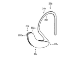
- FIG. 16 is a perspective view showing the configuration of the probe 20h according to the second embodiment.
- symbol is attached
- a probe 20h shown in FIG. 16 has a substantially flat plate shape with a uniform plate thickness, and is formed by laminating a metal plate 201f and a metal plate 202g corresponding to the metal plate 201 and the metal plate 202, respectively, in the thickness direction.
- 1 has an arc-shaped side surface at the tip, and has a first contact portion 21 in contact with the semiconductor integrated circuit 100 shown in FIG. 1 and an arc-shaped side surface on this side surface.
- the second contact portion 28 that contacts the circuit board 30, the connection portion 23 that connects the first contact portion 21 and the second contact portion 28, and the second contact portion 28, part of which forms an arc shape, And an elastic portion 24 that is elastically deformed by a load applied to the portion 21 and the second contact portion 28.
- the second contact portion 28 has a side surface 28a formed in a plane corresponding to the wall surface of the fixing member 13, and fixes the probe 20h by coming into contact with the wall surface of the fixing member 13.
- FIG. 17 is a partial cross-sectional view showing a case where the probe 20h shown in FIG. 16 is introduced into the probe unit 1 shown in FIG.
- the probe 20h held in the hole 14 of the fixing member 13 is in contact with the wall surface of the fixing member 13 at the side surface 28a also in the second contact portion 28.
- the side surface 28 a is formed along the wall surface of the fixing member 13, the protruding direction of the connection portion 23 and the first contact portion 21 from the slit 12 is adjusted by the contact of the second contact portion 28. It becomes possible.
- the side surface 28a contacting the wall surface of the fixing member 13 has a positioning effect. It can be easily disposed at a predetermined position.
- the probe 20 shown in FIG. 5 or the probes 20 a to 20 g shown in FIGS. 9 to 15 may be brought into contact with the wall surface of the fixing member 13.
- the positioning effect can be obtained by bringing the second contact portion 22 or the second contact portions 22a to 22c into contact with the wall surface of the fixing member 13.
- the semiconductor integrated circuit has been described as being a QFN having no external lead.
- the semiconductor integrated circuit 102 having a lead 103 (Quad Flat) Package: QFP).
- the contact probe and the probe unit according to the present invention are useful when electrical connection is made by connecting electrical circuit boards or the like.
- Probe unit 10 Probe holder 11 Storage part 12 Slit 13 Fixing member 14 Hole part 15 Opening part 20,20a, 20b, 20c, 20d, 20e, 20f, 20g, 20h Probe 21,21a, 21b, 21c 1st contact part 22 , 22a, 22b, 22c, 28 Second contact portion 23, 23a, 26 Connection portion 24, 24a, 25, 27, 27a, 27b Elastic portion 30 Circuit board 31, 101 Electrode 100, 102 Semiconductor integrated circuit 103 Lead 201, 201a ⁇ 201f, 202,202a ⁇ 202g Metal plate
Landscapes
- Engineering & Computer Science (AREA)
- Computer Hardware Design (AREA)
- Microelectronics & Electronic Packaging (AREA)
- Physics & Mathematics (AREA)
- General Physics & Mathematics (AREA)
- Measuring Leads Or Probes (AREA)
Abstract
異なる基板間を接続する板状のコンタクトプローブ(20)であって、先端部で弧状に湾曲した側面を有し、この側面で一方の基板と接触する第1接触部(21)と、弧状に湾曲した側面を有し、この側面で他方の基板と接触する第2接触部(22)と、第1接触部(21)および第2接触部(22)を接続する接続部(23)とを有する導通部と、使用環境温度の最大値以上の最高使用温度を有する金属板(201)を用いて形成され、第2接触部(22)から延び、一部が弧状に湾曲された形状をなし、第1接触部(21)および第2接触部(22)に加わる荷重によって弾性変形する弾性部(24)と、を備え、導通部は、弾性部(24)と異なる導電性材料である金属板(202)を含む。
Description
本発明は、電気回路基板間等の接続に用いられるコンタクトプローブおよびプローブユニットに関するものである。
従来、半導体集積回路や液晶パネルなどの検査対象の導通状態検査や動作特性検査を行う際には、検査対象と検査用信号を出力する信号処理装置との間の電気的な接続を図るために、導電性のコンタクトプローブを複数収容するプローブユニットが用いられる。プローブユニットにおいては、近年の半導体集積回路や液晶パネルの高集積化、微細化の進展に伴い、コンタクトプローブ間のピッチを狭小化することにより、高集積化、微細化された検査対象にも適用可能な技術が進歩してきている。
コンタクトプローブ間のピッチを狭小化する技術として、例えばコンタクトプローブの外部からの荷重に応じて屈曲可能な弾性を備えたワイヤー型のコンタクトプローブに関する技術が知られている。ワイヤー型のコンタクトプローブは、バネを用いたピン型のコンタクトプローブと比較して細径化が容易であるが、荷重が加わった時に撓む方向が揃っていないと、隣接するコンタクトプローブ同士が接触したり被接触体との接触にバラツキが生じたりしてしまう恐れがある。このため、ワイヤー型のコンタクトプローブにおいては、荷重によって撓む方向を一様に揃えるための様々な工夫が施されている。
このうち、特許文献1では、コンタクトプローブに対してゴムまたは樹脂によって形成されるエラストマが設けられ、コンタクトプローブと電極等との接触によってエラストマが弾性変形し、コンタクトプローブと電極との接触状態を維持している。
また、特許文献2では、接触体との接触間に湾曲した形状をなしてバネ性を有する複数のコンタクトプローブがテストボードに収容されているプローブユニットが開示されている。このコンタクトプローブは、バネ性を有する部分と電気信号の導通部分とが共通している。
ところで、半導体集積回路や液晶パネルなどの検査対象の導通状態検査や動作特性検査の評価基準は、年々厳しくなってきている。これらの検査を行なう際の使用環境温度は、-40~200℃という広範囲にわたり、コンタクトプローブを含む検査装置側においてもこれらの温度での耐久性が求められてきている。
しかしながら、特許文献1が開示するコンタクトプローブでは、高温領域に対する耐久性の低いエラストマが用いられているため、上述した使用環境温度における高温領域で試験を行なった場合、コンタクトプローブ自体の耐久性も低下してしまうおそれがあった。
また、特許文献2が開示するコンタクトプローブでは、全体が金属によって形成されているものの、バネ性を確保するにはコンタクトプローブ自体を長くしなければならず、電気抵抗が大きくなって導通性が悪くなるという問題があった。
本発明は、上記に鑑みてなされたものであって、バネ性を有し、接触対象間で確実かつ良好な導通を得ることができるとともに、高温領域に対する耐久性を向上することができるコンタクトプローブおよびプローブユニットを提供することを目的とする。
上述した課題を解決し、目的を達成するために、本発明にかかるコンタクトプローブは、異なる基板間を接続する板状のコンタクトプローブであって、一方の基板と接触する第1接触部と、他方の基板と接触する第2接触部と、前記第1接触部および前記第2接触部を接続する接続部とを有し、異なる基板同士を導通させる導通部と、当該コンタクトプローブの使用環境温度の最大値以上の最高使用温度を有する金属材料を用いて形成され、前記第2接触部から延び、前記第1接触部および前記第2接触部に加わる荷重によって弾性変形する弾性部と、を備え、前記導通部は、前記金属材料と異なる導電性材料を含むことを特徴とする。
また、本発明にかかるコンタクトプローブは、上記の発明において、前記導電性材料は、前記金属材料と比して電気伝導度の大きい金属または合金であることを特徴とする。
また、本発明にかかるコンタクトプローブは、上記の発明において、前記導通部は、互いに板状をなす前記導電性材料と前記金属材料とが厚さ方向に積層されてなることを特徴とする。
また、本発明にかかるコンタクトプローブは、上記の発明において、前記弾性部は、互いに板状をなす前記金属材料と前記導電性材料とが厚さ方向に積層されてなることを特徴とする。
また、本発明にかかるコンタクトプローブは、上記の発明において、前記第1および第2接触部は、前記導電性材料が前記金属材料よりも外縁側に突出していることを特徴とする。
また、本発明にかかるコンタクトプローブは、上記の発明において、前記弾性部の幅は、前記接続部の幅と比して小さいことを特徴とする。
また、本発明にかかるコンタクトプローブは、上記の発明において、前記金属材料は、耐熱鋼、超合金または電鋳材であることを特徴とする。
また、本発明にかかるコンタクトプローブは、上記の発明において、前記弾性部は、前記第1接触部と接する第1の平面と、前記第1の平面と平行であって、前記第2接触部と接する第2の平面との間に位置することを特徴とする。
また、本発明にかかるコンタクトプローブは、上記の発明において、前記弾性部は、一部が直線状をなすことを特徴とする。
また、本発明にかかるプローブユニットは、上記の発明にかかるコンタクトプローブと、前記コンタクトプローブを保持する保持部と、を備えたことを特徴とする。
本発明にかかるコンタクトプローブおよびプローブユニットは、導通性を有する部分とバネ性を有する部分とをコンタクトプローブの異なる位置がそれぞれ担い、導通性を有する部分が、耐熱鋼、超合金または電鋳材等の金属材料を用いて形成されるバネ性を有する部分と異なる導電性材料を含むようにしたので、バネ性を有し、接触対象間で確実かつ良好な導通を得ることができるとともに、高温領域に対する耐久性を向上することができるという効果を奏する。
以下、本発明を実施するための形態を図面と共に詳細に説明する。なお、以下の実施の形態により本発明が限定されるものではない。また、以下の説明において参照する各図は、本発明の内容を理解でき得る程度に形状、大きさ、および位置関係を概略的に示してあるに過ぎない。すなわち、本発明は各図で例示された形状、大きさ、および位置関係のみに限定されるものではない。
(実施の形態1)
図1は、本発明の実施の形態1にかかるプローブユニットの構成を示す斜視図である。図1に示すプローブユニット1は、検査対象物である半導体集積回路100の電気特性検査を行う際に使用する装置であって、半導体集積回路100と半導体集積回路100へ検査用信号を出力する回路基板30との間を電気的に接続する装置である。なお、本実施の形態1において、半導体集積回路100は、電極101を有するQFN(Quad Flat Non‐leaded Package)であるものとして説明する。
図1は、本発明の実施の形態1にかかるプローブユニットの構成を示す斜視図である。図1に示すプローブユニット1は、検査対象物である半導体集積回路100の電気特性検査を行う際に使用する装置であって、半導体集積回路100と半導体集積回路100へ検査用信号を出力する回路基板30との間を電気的に接続する装置である。なお、本実施の形態1において、半導体集積回路100は、電極101を有するQFN(Quad Flat Non‐leaded Package)であるものとして説明する。
プローブユニット1は、異なる二つの被接触体(基板)である半導体集積回路100および回路基板30に接触する導電性のコンタクトプローブ20(以下、単に「プローブ20」という)と、複数のプローブ20を所定のパターンにしたがって収容して保持する保持部としてのプローブホルダ10と、プローブホルダ10の底部に当接し、プローブ20を介して半導体集積回路100へ検査用信号を出力する回路基板30とを有する。
回路基板30は、図2に示すように、プローブ20を介して半導体集積回路100へ検査用信号を出力するための電極31を有する。電極31は、プローブホルダ10に保持されたプローブ20に対応して回路基板30上に配設される。なお、プローブホルダ10と回路基板30とは、ネジ等によって接続されてもよく、接着剤またはシール部材によって接着されてもよい。プローブ20と電極31との接触を妨げなければ、如何なる接着形態でもよい。
プローブホルダ10は、絶縁性材料を用いて形成され、半導体集積回路100を収容可能な収容空間が形成された収容部11と、プローブ20を所定パターンで保持するためのスリット12とを有する。スリット12は、収容部11側にプローブ20の先端が突出するようにプローブ20を保持する。また、スリット12は、収容部11に半導体集積回路100が収容された場合、各プローブ20が、対応する半導体集積回路100の電極101と接触する位置に形成される。
図3は、図1に示すプローブユニット1の要部の構成を示す分解斜視図である。図4は、図1に示すプローブユニット1の要部の構成を示す斜視図である。プローブホルダ10は、図3,4に示すように、底部外周にプローブ20を固定する固定部材13が着脱可能に連結されて構成されている。固定部材13は、絶縁性材料を用いて形成され、プローブホルダ10と比して大きい開口部15と、プローブ20を保持して固定する穴部14とを有する。プローブホルダ10は、固定部材13に応じた切り欠き部分で固定部材13と嵌合することで長方体形状をなし、プローブ20を保持する保持部を構成する。穴部14は、スリット12に挿通されたプローブ20の端部を収容し、収容部11の所定位置にプローブ20の他方の先端部分が位置するようプローブ20を保持する。なお、プローブ20を所定間隔および所定方向に固定することが可能であれば、保持部の構成を固定部材13のみとしてもよく、プローブユニット10と固定部材13の穴部14とを一体成形してもよい。
図5は、本発明の実施の形態1にかかるプローブ20を示す斜視図である。また、図6は、図1に示すスリット12の中央を通過する平面で切断した断面図である。図5,6に示すプローブ20は、板厚が均一な略平板状をなす金属板201と金属板202とが厚さ方向に積層されてなり、先端部で弧状をなす側面を有し、この側面で半導体集積回路100と接触する第1接触部21と、弧状をなす側面を有し、この側面で回路基板30と接触する第2接触部22と、第1接触部21および第2接触部22を接続する帯状の接続部23とを有する導通部と、第2接触部22から延び、一部が弧状をなし、第1接触部21および第2接触部22に加わる荷重によって弾性変形する弾性部24と、を備える。
第2接触部22の弧状をなす側面は、図6に示す断面図のように、プローブホルダ10に保持されて回路基板30の電極31に当接する。
弾性部24は、接続部23の幅と比して小さい幅を有する。このため、弾性部24は、第1接触部21または第2接触部22に加わる荷重に対して他の部分よりも弾性変形を生じやすい。なお、弾性部24の幅と接続部23の幅との比は、弾性部24が優先的に弾性変形可能であれば、如何なる比であってもよい。また、弾性部24の第2接触部22と異なる方向の端部は、直線状をなして延びており、この直線状部分の先端部が穴部14に差し込んで取り付けられて、プローブ20がプローブホルダ10に保持される。
金属板201を形成する金属材料としては、例えば、使用環境温度の最大値が200℃程度の場合、最高使用温度が200℃以上の耐熱鋼、超合金または電鋳材が挙げられる。この耐熱鋼としては、オーステナイト系ステンレス鋼、合金工具鋼、析出硬化系ステンレス鋼等が挙げられる。また、超合金としては、ニッケル基およびコバルト基をそれぞれ主成分とする合金であるニッケル基超合金、コバルト基超合金およびニッケル-コバルト系超合金等が挙げられる。なお、プローブの使用環境温度の最大値が200℃程度の場合、例えば、融点が600℃以上の金属等を用いることもできる。このような金属の例として、ニッケル系の電鋳材を挙げることができる。ここで、最高使用温度は、加熱に対する線収縮率から求められる量であり、材料の耐熱特性を示す量である。
また、金属板202を形成する金属としては、電気抵抗率が1.0×10⁻⁷Ω・m以下である金属または合金等の導電性材料が挙げられる。この金属としては、例えば、金、銅、ニッケル、銀、白金、ロジウム等が挙げられる。なお、金属板201を形成する金属材料と比して電気伝導度が大きい金属または合金であれば適用可能である。
上述した金属板201および金属板202においては、金属板201によって、高温状態において弾性部24の弾性変形が維持されることによるプローブ20の変形を抑制し、金属板202によって、導通部における確実かつ良好な電気的導通を行なうことができる。
図7は、第1接触部21または第2接触部22に荷重が加わった状態を示す部分断面図である。図7に示すように、第1接触部21が半導体集積回路100の電極101と接触して図中の矢印方向に荷重が加わると、弾性部24の湾曲部分が弾性変形する。ここで、破線P0は、図6に示す荷重が加わっていない状態でのプローブ20の位置を示している。
第1接触部21に外部からの荷重が加わると、第1接触部21、第2接触部22(接続部23を含む)は弾性変形することなく、荷重に応じて電極101、電極31と当接しながら移動する。また、弾性部24は、接続部23および第2接触部22を介して伝達される荷重に応じて弾性変形を生ずる。なお、このときに流れる電流の導通箇所は、第1接触部21、接続部23および第2接触部22となり、弾性部24に電流は導通しない。
図8は、第1接触部21に荷重が加わって弾性部24が弾性変形しているときの第1接触部21と電極101との接触状態および第2接触部22と電極31との接触状態を説明する図である。まず、図8(a)は、第1接触部21に対して半導体集積回路100の電極101が当接した状態(荷重が加わっていない状態)を示している。この場合の第1接触部21と電極101との接触点をS0、第2接触部22と電極31との接触点をC0とする。
図8(a)において、半導体集積回路100が矢印方向に移動すると、第1接触部21に荷重が加わり、第1接触部21が押し下げられる。この第1接触部21の移動によって第1接触部21および第2接触部22の各電極101,31との接触点がそれぞれS1,C1にずれる(図8(b))。なお、破線P0は、図8(a)に示す荷重が加わっていない状態でのプローブ20の位置を示し、破線I0は、図8(a)に示す半導体集積回路100の位置を示している。
ここで、第1接触部21および第2接触部22は、各電極101,31上を回転して接触点が移動する。このため、各接触部は各電極に対して与える摩擦力等が小さく、接触部および電極それぞれの磨耗を抑制することが可能となる。
半導体集積回路100を図8(b)に示す矢印の向き(図中下向き)に移動させると、第1接触部21がさらに押し下げられ、図8(b)と同様、第1接触部21および第2接触部22の各電極101,31との接触点がそれぞれS2,C2にずれる(図8(c))。
上述した実施の形態1にかかるプローブユニット1は、異なる金属を積層させ、同一プローブ内で電気的導通を行なう部分とバネ性を有する部分とを異なる形状としたので、バネ性の確保によって電気的な導通経路が長くなることなく、プローブの設計を行なうことができ、確実な電気的導通を行なうとともに、高温状態での繰り返しの使用または長時間にわたる加圧によるプローブの変形を防止することが可能となる。また、各接触部が電極との接触に対して回転して接点を移動させるため、接触部と電極との間の摩擦を軽減し、接触部および電極の磨耗を抑制することができる。
なお、上述したプローブ20において、金属板201と金属板202の積層関係が逆の構成であってもよいし、1枚の金属板201と金属板202とが張り合わせられた構成であってもよいし、4層以上の複数の金属板が積層される構成であってもよい。
また、上述した実施の形態1にかかるプローブは、弾性部24側を金属板201で形成し、導通部を金属板202で形成した後、金属板201と金属板202とを接続した構成であってもよい。
図9は、本実施の形態1の変形例1であるプローブ20aを示す平面図である。図9に示すプローブ20aは、第1接触部21aおよび第2接触部22aにおいて、第1接触部21aと第2接触部22aとの間の電気的導通を行なう金属板202が、金属板201よりも外縁側に突出した形状をなしている。これにより、第1接触部21aおよび第2接触部22aにおいて金属板202が各電極と接触するため、一段と確実な電気的導通を得ることが可能となる。
図10は、本実施の形態1の変形例2であるプローブ20bを示す斜視図である。図10に示すプローブ20bは、上述した形状をなす金属板201に対して、導通部に該当する部分に上述した金属板202の形成材料で形成される金属板202aが積層されている。これにより、弾性部24aにおけるバネ性および確実な電気的導通を確保するとともに、弾性部24aにおけるプローブ20bの形成材料の削減によって、製造にかかるコストの削減を行なうことができる。
なお、プローブの形状は、弾性部がバネ性を有するものであれば、如何なる形状でもよい。図11は、本実施の形態1の変形例3であるプローブ20cを示す斜視図である。
プローブ20cは、図11に示すように、上述した金属板201と金属板202とにそれぞれ対応する金属板201aと金属板202bとが積層されてなり、第1接触部21および第2接触部22と、第1接触部21と第2接触部22とを接続する接続部23と、一部が弧状をなし、第1接触部21および第2接触部22に加わる荷重によって弾性変形する弾性部25と、を備える。
弾性部25は、両端部側で直線状をなす部分が平行となるように湾曲されて形成される。また、弾性部25の湾曲部分の曲率半径は、図5に示す弾性部24の曲率半径と比して小さい。なお、弾性部25の幅は、接続部23の幅と比して小さい幅となる。
上述したプローブ20cは、弾性部25の湾曲部が小さいため、装置の小型化を行なう場合に有効である。また、プローブ20と半導体集積回路100との接触方向が、図7,8に示すような方向の場合において、半導体集積回路100の移動方向に対して弾性部25の湾曲部分の形成領域が接続部23の形成領域と重なっていないため、接続部23を短くすることによってプローブをさらに小型化することができる。
図12は、本実施の形態1の変形例4であるプローブ20dを示す斜視図である。プローブ20dは、図10に示すように、上述した金属板201と金属板202とにそれぞれ対応する金属板201bと金属板202cとが積層されてなり、上述した第1接触部21および第2接触部22に対応する第1接触部21cおよび第2接触部22cと、第1接触部21cと第2接触部22cとを接続する直線状をなす接続部26と、一部が弧状をなし、第1接触部21cおよび第2接触部22cに加わる荷重によって弾性変形する弾性部24と、を備える。
プローブ20dは、上述した実施の形態1と同様の効果を有するとともに、第2接触部22cの電極との接触部分の曲率半径が小さく、電極上を回転する距離が短くなるため、特に、電極のサイズが小さい場合に有用である。また、接続部26は、上述した弧状の接続部23と比して導通距離が短くなるため、一段と安定した導通を得ることができる。
図13は、本実施の形態1の変形例5であるプローブ20eを示す斜視図である。プローブ20eは、図13に示すように、上述した金属板201と金属板202とにそれぞれ対応する金属板201cと金属板202dとが積層されてなり、上述した第1接触部21および第2接触部22と、第1接触部21と第2接触部22とを接続する接続部23と、第2接触部22から延び、一部が弧状をなし、第1接触部21および第2接触部22に加わる荷重によって弾性変形する弾性部27と、を備える。なお、弾性部27の幅は、接続部23の幅と比して小さい幅となる。また、弾性部27の第2接触部22と異なる方向の端部は、直線状をなして延びている。
弾性部27は、第1接触部21と接する第1の平面G1と、第1の平面G1に平行であって、第2接触部22と接する第2の平面G2との間に位置する。すなわち、弾性部27は、第2の平面G2から、弾性部27の第2の平面G2に最も遠い点までの距離d2が、第1の平面G1と第2の平面G2との間の距離d1より小さくなるように湾曲されて形成される。
プローブ20eは、上述した実施の形態1と同様の効果を有するとともに、例えばプローブ20eがプローブホルダ1に保持されて検査を行う場合、弾性部27の形成領域を含む領域において上方から半導体集積回路100が接近した場合であっても、弾性部27と半導体集積回路100とが接触することなく、検査を行うことが可能となる。
また、図14に示す変形例6のように、凹凸が逆の湾曲部分を繰り返してジグザグ状に延びる形状をなす弾性部27aを有するプローブ20fであってもよい。プローブ20fは、上述した金属板201と金属板202とにそれぞれ対応する金属板201dと金属板202eとが積層されてなる。弾性部27aは、平面G1,G2と略直交する方向に往復して、平面G1,G2と平行な方向に延びる形状をなす。この場合も、第2の平面G2から、弾性部27aの第2の平面G2に最も遠い点までの距離d3が、第1の平面G1と第2の平面G2との間の距離d1より小さくなるように湾曲されて形成される。
また、図15に示す変形例7のように、凹凸が逆の湾曲部分を繰り返してジグザグ状に延びる形状をなす弾性部27bを有するプローブ20gであってもよい。プローブ20gは、上述した金属板201と金属板202とにそれぞれ対応する金属板201eと金属板202fとが積層されてなる。弾性部27bは、平面G1,G2と平行な方向に往復して、平面G1,G2と垂直な方向に延びる形状をなす。この場合も、第2の平面G2から、弾性部27bの第2の平面G2に最も遠い点までの距離d4が、第1の平面G1と第2の平面G2との間の距離d1より小さくなるように湾曲されて形成される。
なお、上述した変形例5~7にかかる弾性部27,27a,27bの形状は、変形例1,2,4の弾性部24,24aに対して適用することもできる。
(実施の形態2)
実施の形態1では、プローブの第2接触部が固定部材の壁面に当接しないものとして説明したが、本実施の形態2では、第2接触部が固定部材の壁面に当接している場合について説明する。図16は、本実施の形態2にかかるプローブ20hの構成を示す斜視図である。なお、図1等で上述したプローブユニット1と同じ構成要素には同じ符号を付してある。
実施の形態1では、プローブの第2接触部が固定部材の壁面に当接しないものとして説明したが、本実施の形態2では、第2接触部が固定部材の壁面に当接している場合について説明する。図16は、本実施の形態2にかかるプローブ20hの構成を示す斜視図である。なお、図1等で上述したプローブユニット1と同じ構成要素には同じ符号を付してある。
図16に示すプローブ20hは、板厚が均一な略平板状をなし、上述した金属板201と金属板202とにそれぞれ対応する金属板201fと金属板202gとが厚さ方向に積層されてなり、先端部で弧状をなす側面を有し、この側面で、図1に示す半導体集積回路100と接触する第1接触部21と、弧状をなす側面を有し、この側面で、図1に示す回路基板30と接触する第2接触部28と、第1接触部21および第2接触部28を接続する接続部23と、第2接触部28から延び、一部が弧状をなし、第1接触部21および第2接触部28に加わる荷重によって弾性変形する弾性部24と、を備える。
第2接触部28は、固定部材13の壁面に対応する平面に形成された側面28aを有し、固定部材13の壁面と当接することでプローブ20hを固定する。図17は、図16に示すプローブ20hを図1に示すプローブユニット1に導入した場合を示す部分断面図である。
図17に示すように、固定部材13の穴部14に保持されたプローブ20hは、第2接触部28においても側面28aで固定部材13の壁面と当接している。このとき、側面28aは、固定部材13の壁面に沿うように形成されているため、第2接触部28の当接によって接続部23および第1接触部21のスリット12からの突出方向を調節することが可能となる。
図18は、半導体集積回路100によって第1接触部21が押し下げられた状態を示す部分断面図である。実施の形態1と同様、電極101と接触した第1接触部21および電極31と接触した第2接触部28は、半導体集積回路100の移動(図中矢印方向)によって、各電極表面上で回転して接触して、半導体集積回路100と回路基板30との間を電気的に導通させる。また、プローブ20hに加わる荷重によって、弾性部24の湾曲部分が弾性変形を生ずる。なお、破線P1は、図17に示す半導体集積回路100からの荷重がかかっていない場合のプローブ20hの位置を示している。
上述した実施の形態2にかかるプローブ20hによって、固定部材13の穴部14に保持された場合に、固定部材13の壁面に当接する側面28aが位置決めの効果を有するため、プローブ20hをプローブユニット1の所定位置に容易に配設することができる。
なお、図5に示すプローブ20または図9~15に示すプローブ20a~20gを固定部材13の壁面に当接させてもよい。固定部材13の壁面に第2接触部22または第2接触部22a~22cを当接させることによって、位置決めの効果を得ることができる。
なお、上述した実施の形態1,2において、半導体集積回路が外部にリードを有しないQFNであるものとして説明してきたが、図19に示すように、リード103を有する半導体集積回路102(Quad Flat Package:QFP)であってもよい。
以上のように、本発明にかかるコンタクトプローブおよびプローブユニットは、電気回路基板間等を接続して、電気的導通を行なう場合に有用である。
1 プローブユニット
10 プローブホルダ
11 収容部
12 スリット
13 固定部材
14 穴部
15 開口部
20,20a,20b,20c,20d,20e,20f,20g,20h プローブ
21,21a,21b,21c 第1接触部
22,22a,22b,22c,28 第2接触部
23,23a,26 接続部
24,24a,25,27,27a,27b 弾性部
30 回路基板
31,101 電極
100,102 半導体集積回路
103 リード
201,201a~201f,202,202a~202g 金属板
10 プローブホルダ
11 収容部
12 スリット
13 固定部材
14 穴部
15 開口部
20,20a,20b,20c,20d,20e,20f,20g,20h プローブ
21,21a,21b,21c 第1接触部
22,22a,22b,22c,28 第2接触部
23,23a,26 接続部
24,24a,25,27,27a,27b 弾性部
30 回路基板
31,101 電極
100,102 半導体集積回路
103 リード
201,201a~201f,202,202a~202g 金属板
Claims (10)
- 異なる基板間を接続する板状のコンタクトプローブであって、
一方の基板と接触する第1接触部と、他方の基板と接触する第2接触部と、前記第1接触部および前記第2接触部を接続する接続部とを有し、異なる基板同士を導通させる導通部と、
当該コンタクトプローブの使用環境温度の最大値以上の最高使用温度を有する金属材料を用いて形成され、前記第2接触部から延び、前記第1接触部および前記第2接触部に加わる荷重によって弾性変形する弾性部と、
を備え、
前記導通部は、前記金属材料と異なる導電性材料を含むことを特徴とするコンタクトプローブ。 - 前記導電性材料は、前記金属材料と比して電気伝導度の大きい金属または合金であることを特徴とする請求項1に記載のコンタクトプローブ。
- 前記導通部は、互いに板状をなす前記導電性材料と前記金属材料とが厚さ方向に積層されてなることを特徴とする請求項1または2に記載のコンタクトプローブ。
- 前記弾性部は、互いに板状をなす前記金属材料と前記導電性材料とが厚さ方向に積層されてなることを特徴とする請求項3に記載のコンタクトプローブ。
- 前記第1および第2接触部は、前記導電性材料が前記金属材料よりも外縁側に突出していることを特徴とする請求項4に記載のコンタクトプローブ。
- 前記弾性部の幅は、前記接続部の幅と比して小さいことを特徴とする請求項1~5のいずれか一つに記載のコンタクトプローブ。
- 前記金属材料は、耐熱鋼、超合金または電鋳材であることを特徴とする請求項1~6のいずれか一つに記載のコンタクトプローブ。
- 前記弾性部は、前記第1接触部と接する第1の平面と、前記第1の平面と平行であって、前記第2接触部と接する第2の平面との間に位置することを特徴とする請求項1~7のいずれか一つに記載のコンタクトプローブ。
- 前記弾性部は、一部が直線状をなすことを特徴とする請求項1~8のいずれか一つに記載のコンタクトプローブ。
- 請求項1~9のいずれか一つに記載のコンタクトプローブと、
前記コンタクトプローブを保持する保持部と、
を備えたことを特徴とするプローブユニット。
Applications Claiming Priority (2)
| Application Number | Priority Date | Filing Date | Title |
|---|---|---|---|
| JP2010-162165 | 2010-07-16 | ||
| JP2010162165 | 2010-07-16 |
Publications (1)
| Publication Number | Publication Date |
|---|---|
| WO2012008541A1 true WO2012008541A1 (ja) | 2012-01-19 |
Family
ID=45469536
Family Applications (1)
| Application Number | Title | Priority Date | Filing Date |
|---|---|---|---|
| PCT/JP2011/066141 Ceased WO2012008541A1 (ja) | 2010-07-16 | 2011-07-14 | コンタクトプローブおよびプローブユニット |
Country Status (2)
| Country | Link |
|---|---|
| TW (1) | TW201217793A (ja) |
| WO (1) | WO2012008541A1 (ja) |
Cited By (2)
| Publication number | Priority date | Publication date | Assignee | Title |
|---|---|---|---|---|
| JP2016038206A (ja) * | 2014-08-05 | 2016-03-22 | 株式会社アイエスシーIsc Co., Ltd. | ポゴピン用プローブ部材 |
| US9726693B2 (en) | 2013-04-18 | 2017-08-08 | Isc Co., Ltd. | Probe member for pogo pin |
Families Citing this family (2)
| Publication number | Priority date | Publication date | Assignee | Title |
|---|---|---|---|---|
| CN108572264B (zh) * | 2018-06-21 | 2023-12-01 | 武汉精测电子集团股份有限公司 | 一种单缓冲通道的压接弹片 |
| CN115060930B (zh) * | 2022-05-25 | 2025-08-19 | 欧拓飞科技(珠海)有限公司 | 一种端子检测插座 |
Citations (4)
| Publication number | Priority date | Publication date | Assignee | Title |
|---|---|---|---|---|
| JPH11344508A (ja) * | 1998-06-02 | 1999-12-14 | Japan Electronic Materials Corp | プローブ及びこのプローブを用いたプローブカード |
| JP2005228496A (ja) * | 2004-02-10 | 2005-08-25 | Neomax Material:Kk | 端子用クラッド材およびその端子用クラッド材によって形成されたアルミニウム電線用端子 |
| JP2007503103A (ja) * | 2003-06-11 | 2007-02-15 | シンチ コネクターズ インコーポレーテッド | 電気コネクタ |
| JP2008309535A (ja) * | 2007-06-13 | 2008-12-25 | Japan Electronic Materials Corp | コンタクトプローブ及びその製造方法 |
-
2011
- 2011-07-14 WO PCT/JP2011/066141 patent/WO2012008541A1/ja not_active Ceased
- 2011-07-15 TW TW100125051A patent/TW201217793A/zh unknown
Patent Citations (4)
| Publication number | Priority date | Publication date | Assignee | Title |
|---|---|---|---|---|
| JPH11344508A (ja) * | 1998-06-02 | 1999-12-14 | Japan Electronic Materials Corp | プローブ及びこのプローブを用いたプローブカード |
| JP2007503103A (ja) * | 2003-06-11 | 2007-02-15 | シンチ コネクターズ インコーポレーテッド | 電気コネクタ |
| JP2005228496A (ja) * | 2004-02-10 | 2005-08-25 | Neomax Material:Kk | 端子用クラッド材およびその端子用クラッド材によって形成されたアルミニウム電線用端子 |
| JP2008309535A (ja) * | 2007-06-13 | 2008-12-25 | Japan Electronic Materials Corp | コンタクトプローブ及びその製造方法 |
Cited By (2)
| Publication number | Priority date | Publication date | Assignee | Title |
|---|---|---|---|---|
| US9726693B2 (en) | 2013-04-18 | 2017-08-08 | Isc Co., Ltd. | Probe member for pogo pin |
| JP2016038206A (ja) * | 2014-08-05 | 2016-03-22 | 株式会社アイエスシーIsc Co., Ltd. | ポゴピン用プローブ部材 |
Also Published As
| Publication number | Publication date |
|---|---|
| TW201217793A (en) | 2012-05-01 |
Similar Documents
| Publication | Publication Date | Title |
|---|---|---|
| WO2011115074A1 (ja) | コンタクトプローブおよびプローブユニット | |
| CN111239447B (zh) | 探针、检查工具、检查单元和检查装置 | |
| JP6110086B2 (ja) | 接触検査装置 | |
| JP6103821B2 (ja) | 通電試験用プローブ | |
| CN102183680B (zh) | 连接装置 | |
| JP2017146119A (ja) | プローブピンおよびこれを用いた検査装置 | |
| CN111856090B (zh) | 探针、检查夹具及检查组件 | |
| WO2012008541A1 (ja) | コンタクトプローブおよびプローブユニット | |
| CN112345802A (zh) | 电触头及电连接装置 | |
| JP2011232313A (ja) | コンタクトプローブおよびプローブユニット | |
| CN115015602A (zh) | 探针、检查工具及检查工具单元 | |
| JP2011133354A (ja) | コンタクトプローブおよびプローブユニット | |
| JP5480717B2 (ja) | 通電検査用プローブ | |
| TW202323827A (zh) | 探針卡 | |
| JP2013148433A (ja) | コンタクトプローブおよびプローブユニット | |
| JP2013061189A (ja) | コンタクトプローブおよびプローブユニット | |
| WO2012063858A1 (ja) | プローブユニット | |
| JP2013061188A (ja) | コンタクトプローブおよびプローブユニット | |
| WO2024122229A1 (ja) | プローブ | |
| JP2013148432A (ja) | コンタクトプローブおよびプローブユニット | |
| WO2012118026A1 (ja) | コンタクトプローブおよびプローブユニット | |
| CN100486046C (zh) | Ic插座 | |
| JP2020076664A (ja) | プローブピン、検査治具、検査ユニットおよび検査装置 | |
| JP2006294281A (ja) | 半導体装置の検査装置 | |
| JP2016212040A (ja) | コンタクト |
Legal Events
| Date | Code | Title | Description |
|---|---|---|---|
| 121 | Ep: the epo has been informed by wipo that ep was designated in this application |
Ref document number: 11806871 Country of ref document: EP Kind code of ref document: A1 |
|
| NENP | Non-entry into the national phase |
Ref country code: DE |
|
| 122 | Ep: pct application non-entry in european phase |
Ref document number: 11806871 Country of ref document: EP Kind code of ref document: A1 |
|
| NENP | Non-entry into the national phase |
Ref country code: JP |