WO2012005011A1 - 固体撮像装置 - Google Patents
固体撮像装置 Download PDFInfo
- Publication number
- WO2012005011A1 WO2012005011A1 PCT/JP2011/003940 JP2011003940W WO2012005011A1 WO 2012005011 A1 WO2012005011 A1 WO 2012005011A1 JP 2011003940 W JP2011003940 W JP 2011003940W WO 2012005011 A1 WO2012005011 A1 WO 2012005011A1
- Authority
- WO
- WIPO (PCT)
- Prior art keywords
- reset
- transistor
- solid
- imaging device
- state imaging
- Prior art date
- Legal status (The legal status is an assumption and is not a legal conclusion. Google has not performed a legal analysis and makes no representation as to the accuracy of the status listed.)
- Ceased
Links
Images






Classifications
-
- H—ELECTRICITY
- H04—ELECTRIC COMMUNICATION TECHNIQUE
- H04N—PICTORIAL COMMUNICATION, e.g. TELEVISION
- H04N25/00—Circuitry of solid-state image sensors [SSIS]; Control thereof
-
- H—ELECTRICITY
- H04—ELECTRIC COMMUNICATION TECHNIQUE
- H04N—PICTORIAL COMMUNICATION, e.g. TELEVISION
- H04N25/00—Circuitry of solid-state image sensors [SSIS]; Control thereof
- H04N25/60—Noise processing, e.g. detecting, correcting, reducing or removing noise
- H04N25/617—Noise processing, e.g. detecting, correcting, reducing or removing noise for reducing electromagnetic interference, e.g. clocking noise
-
- H—ELECTRICITY
- H04—ELECTRIC COMMUNICATION TECHNIQUE
- H04N—PICTORIAL COMMUNICATION, e.g. TELEVISION
- H04N25/00—Circuitry of solid-state image sensors [SSIS]; Control thereof
- H04N25/60—Noise processing, e.g. detecting, correcting, reducing or removing noise
- H04N25/65—Noise processing, e.g. detecting, correcting, reducing or removing noise applied to reset noise, e.g. KTC noise related to CMOS structures by techniques other than CDS
-
- H—ELECTRICITY
- H04—ELECTRIC COMMUNICATION TECHNIQUE
- H04N—PICTORIAL COMMUNICATION, e.g. TELEVISION
- H04N25/00—Circuitry of solid-state image sensors [SSIS]; Control thereof
- H04N25/70—SSIS architectures; Circuits associated therewith
- H04N25/709—Circuitry for control of the power supply
-
- H—ELECTRICITY
- H04—ELECTRIC COMMUNICATION TECHNIQUE
- H04N—PICTORIAL COMMUNICATION, e.g. TELEVISION
- H04N25/00—Circuitry of solid-state image sensors [SSIS]; Control thereof
- H04N25/70—SSIS architectures; Circuits associated therewith
- H04N25/76—Addressed sensors, e.g. MOS or CMOS sensors
- H04N25/767—Horizontal readout lines, multiplexers or registers
-
- H—ELECTRICITY
- H04—ELECTRIC COMMUNICATION TECHNIQUE
- H04N—PICTORIAL COMMUNICATION, e.g. TELEVISION
- H04N25/00—Circuitry of solid-state image sensors [SSIS]; Control thereof
- H04N25/70—SSIS architectures; Circuits associated therewith
- H04N25/76—Addressed sensors, e.g. MOS or CMOS sensors
- H04N25/78—Readout circuits for addressed sensors, e.g. output amplifiers or A/D converters
-
- H—ELECTRICITY
- H10—SEMICONDUCTOR DEVICES; ELECTRIC SOLID-STATE DEVICES NOT OTHERWISE PROVIDED FOR
- H10F—INORGANIC SEMICONDUCTOR DEVICES SENSITIVE TO INFRARED RADIATION, LIGHT, ELECTROMAGNETIC RADIATION OF SHORTER WAVELENGTH OR CORPUSCULAR RADIATION
- H10F39/00—Integrated devices, or assemblies of multiple devices, comprising at least one element covered by group H10F30/00, e.g. radiation detectors comprising photodiode arrays
- H10F39/10—Integrated devices
- H10F39/12—Image sensors
- H10F39/18—Complementary metal-oxide-semiconductor [CMOS] image sensors; Photodiode array image sensors
-
- H—ELECTRICITY
- H10—SEMICONDUCTOR DEVICES; ELECTRIC SOLID-STATE DEVICES NOT OTHERWISE PROVIDED FOR
- H10F—INORGANIC SEMICONDUCTOR DEVICES SENSITIVE TO INFRARED RADIATION, LIGHT, ELECTROMAGNETIC RADIATION OF SHORTER WAVELENGTH OR CORPUSCULAR RADIATION
- H10F39/00—Integrated devices, or assemblies of multiple devices, comprising at least one element covered by group H10F30/00, e.g. radiation detectors comprising photodiode arrays
- H10F39/80—Constructional details of image sensors
- H10F39/803—Pixels having integrated switching, control, storage or amplification elements
-
- H—ELECTRICITY
- H10—SEMICONDUCTOR DEVICES; ELECTRIC SOLID-STATE DEVICES NOT OTHERWISE PROVIDED FOR
- H10F—INORGANIC SEMICONDUCTOR DEVICES SENSITIVE TO INFRARED RADIATION, LIGHT, ELECTROMAGNETIC RADIATION OF SHORTER WAVELENGTH OR CORPUSCULAR RADIATION
- H10F39/00—Integrated devices, or assemblies of multiple devices, comprising at least one element covered by group H10F30/00, e.g. radiation detectors comprising photodiode arrays
- H10F39/80—Constructional details of image sensors
- H10F39/803—Pixels having integrated switching, control, storage or amplification elements
- H10F39/8037—Pixels having integrated switching, control, storage or amplification elements the integrated elements comprising a transistor
Definitions
- the present invention relates to a solid-state imaging device, and more particularly to a stacked solid-state imaging device.
- an embedded photodiode structure is used as a light receiving portion.
- Patent Document 1 a photoelectric conversion layer is formed on a control electrode constituting a solid-state imaging device, a transparent electrode layer is provided thereon, and the action of the voltage applied thereto is applied to the control electrode through the conversion layer.
- a technique for changing optical information into an electrical signal with a good S / N ratio, a so-called stacked solid-state imaging device is disclosed.
- the stacked solid-state imaging device has a configuration in which a photoelectric conversion film is formed on a semiconductor substrate on which a pixel circuit is formed via an insulating film. For this reason, it is possible to use a material having a large light absorption coefficient such as amorphous silicon for the photoelectric conversion film. For example, in the case of amorphous silicon, green light having a wavelength of 550 nm can be almost absorbed with a thickness of about 0.4 nm.
- the capacity of the photoelectric conversion unit can be increased and the saturation charge can be increased. Furthermore, since the charge is not completely transferred, it is possible to add an additional capacity positively, a sufficiently large capacity can be realized even in a miniaturized pixel, and like a stack cell in a dynamic random access memory. A simple structure is also possible.
- the photoelectric conversion film is formed at a distance from the surface of the semiconductor substrate, and it is necessary to electrically couple the photoelectric conversion film and the surface of the semiconductor substrate. For this reason, there is a problem that the value of dark current, which was not a problem in the embedded photodiode (PD), becomes large.
- the solid-state imaging device includes an amplifying transistor that functions as a driving element for each pixel.
- transistor characteristics in a state where there is no signal charge for example, a threshold voltage of the transistor (hereinafter referred to as Vth) varies.
- Vth a threshold voltage of the transistor
- the stacked solid-state imaging device has a problem that random noise occurs due to capacitive coupling between the reset signal line and the pixel electrode due to the trailing edge of the reset pulse included in the reset signal. is doing.
- the trailing edge (rear edge) of the reset pulse is a falling edge when the reset pulse included in the reset signal is a positive pulse (upward pulse), and the reset pulse is a negative pulse (downward pulse). The case is a rising edge.
- an object of the present invention is to realize a stacked solid-state imaging device capable of suppressing noise such as random noise and fixed pattern noise.
- a solid-state imaging device includes a plurality of pixels arranged in a matrix on a semiconductor substrate, a row scanning unit that generates a row reset signal, and an inversion formed for each column.
- the pixel includes a reset transistor, a selection transistor, an amplification transistor, and a photoelectric conversion unit.
- the photoelectric conversion unit includes a photoelectric conversion film that performs photoelectric conversion, and a photoelectric conversion film on the semiconductor substrate side of the photoelectric conversion film.
- the amplitude of the row reset signal is (a) the maximum voltage applied to the drain of the amplification transistor, (b) the maximum voltage applied to the gate of the selection transistor, and (c) the power supply voltage applied to the inverting amplifier. And (d) less than at least one of the maximum voltages applied to the transparent electrode.
- the row reset signal has an amplitude smaller than at least one of the above (a) to (d), random noise generated due to the trailing edge of the reset pulse included in the reset signal can be suppressed. Can do.
- the solid-state imaging device further feeds back a column signal line formed for each column, an inverting amplifier connected to the column signal line, and an output signal of the inverting amplifier to pixels in the corresponding column.
- a feedback line provided for each column, and the amplification transistor has a gate connected to the pixel electrode, and a signal voltage corresponding to the potential of the pixel electrode is supplied to the column signal via the selection transistor.
- the reset transistor may be connected to the pixel electrode, and the other of the source and the drain may be connected to the corresponding feedback line.
- the reset noise generated when the reset transistor resets the signal charge of the pixel electrode is suppressed, and the reset noise is superimposed on the next signal charge. Since it is reduced, random noise can be suppressed. Also, noise due to circuit variation (for example, Vth unevenness of the amplification transistor for each column) can be reduced by feedback.
- the row scanning unit may further receive a row reset signal before the waveform adjustment having an amplitude corresponding to the power supply voltage, and adjust the waveform so as to reduce the amplitude of the row reset signal.
- the amplitude of the row reset signal applied to the gate of the reset transistor may be smaller than the maximum voltage applied to the drain of the amplification transistor.
- the amplitude of the row reset signal applied to the gate of the reset transistor may be smaller than the maximum voltage applied to the gate of the selection transistor.
- the amplitude of the row reset signal applied to the gate of the reset transistor may be smaller than the power supply voltage applied to the inverting amplifier.
- the amplitude of the row reset signal applied to the gate of the reset transistor may be smaller than the maximum voltage applied to the transparent electrode.
- the amplitude of the row reset signal applied to the gate of the reset transistor is (a) a maximum voltage applied to the drain of the amplification transistor, (b) a maximum voltage applied to the gate of the selection transistor, The voltage may be smaller than (c) a power supply voltage applied to the inverting amplifier and (d) a maximum voltage applied to the transparent electrode.
- the solid-state imaging device further includes a waveform adjustment unit that adjusts a waveform of a row reset signal to be applied to the gate of the reset transistor, and the waveform adjustment unit is configured to output a reset pulse included in the row reset signal.
- the waveform may be adjusted to give a slope to the trailing edge, and the adjusted reset pulse may be supplied to the gate of the reset transistor.
- the solid-state imaging device can switch between imaging at a first frame rate and imaging at a second frame rate higher than the first frame rate, and the waveform adjustment unit
- the slope of the falling edge is set so that the transition time required for the trailing edge or rising edge of the reset pulse in imaging at the first frame rate is greater than the transition time in imaging at the second frame. It is good also as a structure to adjust.
- the waveform adjusting unit may be a filter circuit inserted in a reset control line connected to the gate of the reset transistor.
- the waveform adjusting unit may adjust the slope of the trailing edge of the reset pulse by changing the circuit constant of the filter circuit.
- the waveform adjustment unit may include a digital-analog converter that outputs an analog signal having a slope at the trailing edge of the reset pulse as the row reset signal.
- the solid-state imaging device further includes a waveform adjustment unit that adjusts a waveform of a row reset signal applied to the gate of the reset transistor, and the waveform adjustment unit is arranged after the reset pulse in the row reset signal. You may make it adjust the frequency band which an edge has.
- the solid-state imaging device includes a plurality of pixels arranged in a matrix on a semiconductor substrate, and a row scanning unit that generates a row reset signal.
- the pixel includes a reset transistor, a selection transistor, an amplification transistor, and a photoelectric conversion unit, and the photoelectric conversion unit is formed on a photoelectric conversion film that performs photoelectric conversion and a surface of the photoelectric conversion film on the semiconductor substrate side.
- a pixel electrode and a transparent electrode formed on a surface opposite to the pixel electrode of the photoelectric conversion film, and the amplification transistor has a gate connected to the pixel electrode, and the pixel electrode A signal voltage corresponding to the potential of the selection transistor is output to the column signal line through the selection transistor, and the driving method enables a row selection signal to the gate of the selection transistor,
- the output signal of the amplification transistor is output to a column signal line, (a) the maximum voltage applied to the drain of the amplification transistor, (b) the maximum voltage applied to the gate of the selection transistor, (c) the inverting amplifier And (d) supplying the row reset signal having an amplitude smaller than at least one of the maximum voltages applied to the transparent electrode to the gate of the reset transistor.
- circuit variation (fixed pattern noise due to Vth unevenness of the amplification transistor for each column) is reduced by the feedback circuit, and the reset amplitude at the time of signal charge reading at reset OFF is 0V.
- a small amplitude in the vicinity of 0 V can reduce capacitance variation (fixed pattern noise) between the reset transistor and the amplification transistor.
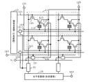
- FIG. 1 is a circuit diagram illustrating the solid-state imaging device according to the first embodiment.
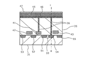
- FIG. 2 is a cross-sectional view illustrating one pixel of the solid-state imaging device according to the first embodiment.
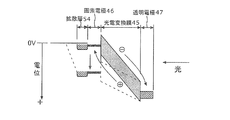
- FIG. 3A is a diagram showing a potential at a portion along line I-II in FIG.
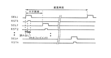
- FIG. 3B is a time chart illustrating the operation of the solid-state imaging device according to the first embodiment.
- FIG. 4A is a potential diagram of a pixel in the prior art.
- FIG. 4B is a potential diagram of a pixel in the second embodiment.
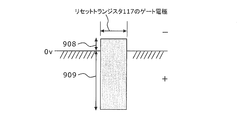
- FIG. 5 is a diagram illustrating the reset amplitude when the reset transistor is controlled.
- FIG. 6A is a circuit diagram illustrating a solid-state imaging device according to the third embodiment.
- FIG. 6B is a time chart illustrating the operation of the solid-state imaging device according to the third embodiment.
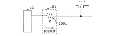
- FIG. 7A is a diagram illustrating a circuit example of the reset signal control element.
- FIG. 7B is a diagram illustrating a circuit example of the reset signal control element.
- FIG. 7C is a diagram illustrating a circuit example of the reset signal control element.
- FIG. 7D is a diagram illustrating a circuit example of the reset signal control element.
- FIG. 7E is a diagram illustrating a circuit example of the reset signal control element.
- the solid-state imaging device of this embodiment is a stacked solid-state imaging device, and FIG. 1 shows a circuit configuration of the solid-state imaging device according to this embodiment.
- FIG. 2 shows a cross-sectional configuration of the pixel 11 of FIG. 1 in the solid-state imaging device of the present embodiment.
- the solid-state imaging device includes a plurality of pixels 11 arranged in a matrix, a vertical scanning unit (also referred to as a row scanning unit) 13 that supplies various timing signals to the pixels 11, A horizontal scanning unit (also referred to as a column scanning unit or a horizontal signal readout unit) 15 that sequentially reads signals to the horizontal output terminal 142, a vertical signal line (also referred to as a column signal line) 141 formed for each column, and a column signal line 141 And the feedback line 126 provided for each column in order to feed back the output signal of the inverting amplifier 23 to the pixel 11 of the corresponding column.
- the pixel 11 describes only two rows and two columns, but the number of rows and the number of columns may be arbitrarily set.
- an amplification transistor 113, a selection transistor 115, and a reset transistor 117 are formed on a semiconductor substrate 31 made of silicon.
- the amplification transistor 113 includes a gate electrode 41, a diffusion layer 51 that is a drain, and a diffusion layer 52 that is a source.
- the selection transistor 115 includes a gate electrode 42, a diffusion layer 52 that is a drain, and a diffusion layer 53 that is a source.
- the source of the amplification transistor and the drain of the selection transistor 115 are a common diffusion layer.
- the reset transistor 117 includes a gate electrode 43, a diffusion layer 55 that is a source, and a diffusion layer 54 that is a drain.
- the diffusion layer 51 and the diffusion layer 54 are separated by the element isolation region 33.
- An insulating film 35 is formed on the semiconductor substrate 31 so as to cover each transistor.
- a photoelectric conversion unit 111 is formed on the insulating film 35.
- the photoelectric conversion unit 111 includes a photoelectric conversion film 45 made of amorphous silicon or the like, a pixel electrode 46 formed on the lower surface of the photoelectric conversion film 45, and a transparent electrode 47 formed on the upper surface of the photoelectric conversion film 45. .
- the pixel electrode 46 is connected to the gate electrode 41 of the amplification transistor 113 and the diffusion layer 54 that is the source of the reset transistor 117 via the contact 36.
- the diffusion layer 54 connected to the pixel electrode 46 functions as a storage diode.
- the pixel 11 has a photoelectric conversion unit 111, an amplification transistor 113 whose gate is connected to the photoelectric conversion unit 111, a reset transistor 117 whose drain is connected to the photoelectric conversion unit 111, and a drain that is connected to the source of the amplification transistor 113. And a selection transistor 115.
- the photoelectric conversion unit 111 includes a photoelectric conversion film 45 that performs photoelectric conversion, a pixel electrode 46 formed on the surface of the photoelectric conversion film 45 on the semiconductor substrate 31 side, and a pixel electrode 46 of the photoelectric conversion film 45. And a transparent electrode 47 formed on the opposite surface.
- the photoelectric conversion unit 111 is connected between the gate of the amplification transistor 113 and the drain of the reset transistor 117, and the photoelectric conversion unit control line 131.
- the amplification transistor 113 is connected to the power source 125 and has a gate connected to the pixel electrode 46, and outputs a signal voltage corresponding to the potential of the pixel electrode 46 to the column signal line 141 via the selection transistor 115.
- One of the source and the drain of the reset transistor 117 is connected to the pixel electrode 46, and the other of the source and the drain is connected to the corresponding feedback line 126.
- the source of the selection transistor 115 is connected to the corresponding vertical signal line 141.
- the gate of the selection transistor 115 is connected to the vertical scanning unit 13 via the address control line 121.
- the gate of the reset transistor 117 is connected to the vertical scanning unit 13 via the reset control line 123.
- the reset transistor 117 is an n-type MOS transistor, the reset pulse included in the reset signal input to the gate thereof is a positive pulse (upward pulse), and the trailing edge of the reset pulse is a falling edge. An example will be described.
- the address control line 121 and the reset control line 123 are provided for each row.
- the photoelectric conversion unit control line 131 is common to all pixels.
- the vertical signal line 141 is provided for each column and is connected to the horizontal signal reading unit 15 through the column signal processing unit 21.
- the column signal processing unit 21 performs noise suppression signal processing typified by correlated double sampling.
- the vertical scanning unit 13 supplies a row reset signal to the gate of the reset transistor 117.
- the amplitude of the row reset signal is (a) the maximum voltage applied to the drain of the amplification transistor, (b) the maximum voltage applied to the gate of the selection transistor, (c) the power supply voltage applied to the inverting amplifier, and (d ) Less than at least one of the maximum voltages applied to the transparent electrode. This is because the random noise generated by the trailing edge (falling edge) of the reset pulse included in the row reset signal is suppressed by making the amplitude of the row reset signal smaller than the amplitude of the other signal lines.
- an inverting amplifier 23 is connected to each vertical signal line 141 provided for each column, and a reference voltage (V R ) 133 common to all pixels is also input to the inverting amplifier 23.
- 23 is connected to the source of the reset transistor 117.
- the selection transistor 115 and the reset transistor 117 are in a conductive state, the output of the selection transistor 115 is received, and the gate potential of the amplification transistor 113 is equal to the reference of the inverting amplifier 23.
- the feedback operation is performed so as to be substantially equal to the voltage (V R ) 133. At this time, the output of the inverting amplifier 23 is 0V or a positive voltage near 0V.
- FIG. 3B is a flowchart showing the most basic imaging operation of the solid-state imaging device.
- SEL1 in the figure indicates a row selection signal for the first row.
- RST1 indicates a row reset signal for the first row.
- SEL2 and RST2 are the same except that the corresponding rows are different.
- the amplitude of the row reset signal is smaller than at least one of the above (a) to (d).
- One horizontal cycle in the figure is a period from when the row selection signal becomes valid until the row selection signal of the next row becomes valid (from the rising edge of SEL1 to the rising edge of SEL2).
- 11 is a period required to read out the signal voltage from 11.
- One vertical cycle is a period required to read out signal voltages from the pixels 11 in all rows.
- the feedback operation occurs when the row selection signal and the row reset signal are enabled at the same time. That is, it occurs when the selection transistor 115 and the reset transistor 117 are simultaneously turned on.
- the vertical scanning unit 13 performs control so that reset (feedback operation) is performed after signal reading from the pixel 11.
- the selection transistor 115 is turned on by enabling the row selection signal to the gate of the selection transistor 115, the output signal of the amplification transistor is output to the column signal line 141, and then the row selection signal becomes effective.
- the output of the inverting amplifier 23 is fed back to the pixel electrode 46 via the reset transistor 117.
- the output of the selection transistor 115 is input to the ⁇ side via the vertical signal line 141 using a differential amplifier circuit such as an operational amplifier, and the reference voltage (V R) is input to the + side.
- V R reference voltage
- the differential amplifier circuit If 133 is input and the output of the differential amplifier circuit is connected to the source of the reset transistor 117, the differential amplifier circuit outputs so that the signal input to the ⁇ side approaches the input signal on the + side. Operate. Note that the inverting amplifier 23 may not be limited to this circuit configuration.
- the present invention uses the photoelectric conversion unit 111 having a large light absorption coefficient, the quantization efficiency is remarkably good, and therefore the effect when the fixed pattern noise is reduced is much greater than that of a solid-state imaging device having a conventional structure. Further, the present invention can reduce the photodiode area, so that the conversion gain can be increased in terms of circuit, and the effect when the fixed pattern noise is lowered is remarkably great. Furthermore, structurally, since the present invention does not perform photoelectric conversion in the semiconductor substrate 31, the effect when the fixed pattern noise is suppressed is remarkably large.
- the voltage applied to the source of the reset transistor 117 becomes 0V or near 0V by performing the feedback operation using the inverting amplifier 23 on each vertical signal line 141.
- the fixed pattern noise of the solid-state imaging device can be reduced, and reading of the signal charge on which the fixed pattern noise is superimposed is also reduced, so that the fixed pattern noise can be suppressed.
- the amplification transistor 113, the selection transistor 115, and the reset transistor 117 are n-channel transistors formed on a p-type semiconductor substrate and having an n-type diffusion layer.
- 31 is a p-type semiconductor substrate
- 41 to 43 and 51 to 55 are n-channel transistors having n-type diffusion layers.
- the amplification transistor 113 is preferably a depletion type transistor.
- the basic circuit configuration can be configured in FIG. 1 of the first embodiment.
- FIG. 3A is a diagram showing a potential at a portion along the line I-II in FIG.
- the potential of the diffusion layer 54 which is a storage diode is approximately 0 V, and a slight reverse bias is applied.
- the reverse bias is about 25 mV caused by thermal noise, part of the charge of the storage diode may escape to the substrate side. For this reason, it is preferable that the reverse bias applied during the period for accumulating signal charges is about 0.1 V or more.
- the reverse leakage current dark current flowing between the storage diode and the semiconductor substrate 31 can be reduced.
- a positive voltage is applied to the transparent electrode 47.
- the voltage changed to the + side by the holes accumulated in the diffusion layer 54 is transmitted to the gate electrode 41 of the amplification transistor 113, and the signal amplified by the amplification transistor 113 is output to the vertical signal line 141 via the selection transistor 115.
- FIG. 4A shows a potential diagram of a general embedded photodiode solid-state imaging device
- FIG. 4B shows a potential diagram of the stacked solid-state imaging device of the present embodiment.
- a general embedded photodiode-type solid-state imaging device accumulates charges 902 (electrons here) on the negative (minus side) with respect to the reference level 903 (for example, 3v). It is necessary to apply a signal.
- the stacked solid-state imaging device applies a positive (plus) voltage to the photoelectric conversion film 45 and charges 905 more positive (plus side) than the reference level 906 (for example, 0 v). Since (here, holes) are accumulated, a reset signal having a small amplitude such as 904 may be applied.
- FIG. 6A is a circuit diagram illustrating the solid-state imaging device according to the present embodiment.
- FIG. 6B is a time chart illustrating the operation of the solid-state imaging device according to the present embodiment.
- FIG. 6A mainly differs from the configuration of the first embodiment (FIG. 1) in that a reset signal control element 151 is added.
- the description of the same points will be omitted, and different points will be mainly described below.
- the reset signal control element 151 is a waveform adjusting unit that adjusts the waveform of the row reset signal to be applied to the gate of the reset transistor 117.
- the reset signal control element (waveform adjustment unit) 151 adjusts the waveform so as to give a slope to the falling edge of the reset pulse included in the row reset signal, and supplies the adjusted row reset signal to the gate of the reset transistor 117. .
- the reset signal control element (waveform adjustment unit) 151 adjusts the frequency band of the falling edge in the row reset signal.
- FIG. 7A to 7E show circuit examples of the reset signal control element 151 shown in FIG. 6A.
- the reset signal control element 151 may be a resistance element R (1001) as shown in FIG. 7A, a filter circuit (RC filter circuit, 1002 and 1003) as shown in FIG. 7B, or a general tapered circuit. It is only necessary to adjust the reset band of the reset signal by adjusting the reset signal input to the gate.
- the reset signal output from the vertical scanning unit 13 is waveform-adjusted using the reset signal control element 151 to adjust the reset band.
- FIG. 7C shows a reset signal control element 151 when a resistance value can be selected using a plurality of resistance elements.
- the resistance value in the reset signal control element 151 is R3> R2> R1, and the reset signal whose reset band is adjusted by passing through the resistance value selected by the selector 1005 by the resistance value selection signal 1004 is the reset transistor 117. Input to the gate.
- the reset signal becomes dull and the time required for resetting becomes longer.
- the reset band can be adjusted according to the shooting scene.
- FIG. 7C shows a case where three types of resistance values can be selected, the number of selectable resistance values is not limited.
- the filter circuit configuration is not limited to this as long as the falling waveform of the reset signal output from the vertical scanning unit 13 can be adjusted. Further, the reset band is adjusted by passing through the filter circuit with a configuration that can be changed to a plurality of filter coefficients (for example, the values of 1002 and 1003 can be changed in a circuit manner as shown in FIG. 7E). A configuration in which the reset signal is input to the gate of the reset transistor 117 is also effective.
- the column signal processing unit 21 on each column signal line 141 converts the analog output of each pixel 11 into a digital signal output.
- the DAC circuit (D / A converter circuit) used therefor may be also used.
- FIG. 5 shows the reset amplitude when the reset transistor 117 is controlled.
- the reset amplitude 908 in the reset OFF state a capacitance variation occurs between the reset transistor 117 and the amplification transistor 113.
- the amplitude in the reset OFF state is 0 V or a small amplitude in the vicinity of 0 V, the capacitance variation can be reduced, and the fixed pattern Noise can be reduced.
- a small amplitude reset signal may be applied to the gate of the reset transistor 117.
- the reset amplitude in the reset OFF state is smaller than the reset amplitude in the reset ON state.
- the reset amplitude in the reset OFF state may be lower than the power supply voltage that drives the amplification transistor 113.
- the reset amplitude in the reset OFF state may be lower than the gate voltage of the selection transistor 115.
- the reset amplitude in the reset OFF state may be lower than the power supply voltage of the inverting amplifier 23.
- a general solid-state imaging device has a first problem caused by a small light absorption coefficient of crystalline silicon and a handling signal amount in order to realize a pixel size of 1 ⁇ m or less.
- the inventors of the present application have found that it is necessary to solve the second problem.
- the light absorption coefficient of crystalline silicon depends on the wavelength of light. Crystal silicon having a thickness of about 3.5 ⁇ m is required for almost completely absorbing and photoelectrically converting green light in the vicinity of a wavelength of 550 nm that determines the sensitivity of the solid-state imaging device. Therefore, the depth of the photodiode formed inside the semiconductor substrate needs to be about 3.5 ⁇ m.
- planar pixel size is 1 ⁇ m
- a problem that light incident obliquely enters a photodiode of an adjacent pixel occurs.
- the amount of signal to be handled is determined by the saturation charge amount of the embedded photodiode which is a photodiode structure used in a general solid-state imaging device.
- the embedded photodiode has the advantage that the signal charge accumulated inside can be transferred almost completely to the adjacent charge detector (complete transfer). For this reason, noise related to charge transfer hardly occurs, and the embedded photodiode is widely used in solid-state imaging devices.
- the number of saturated electrons of 10,000 electrons per pixel is necessary, but when the pixel size is about 1.4 ⁇ m, the number of saturated electrons is limited to about 5000 electrons. At present, it is possible to reduce the number of saturated electrons by creating an image by noise suppression processing using a digital signal processing technique, but it is difficult to obtain a natural reproduced image.
- a high-quality single-lens reflex camera requires a saturation electron number of about 30,000 electrons per pixel.
- the solid-state imaging device since the solid-state imaging device according to the embodiment of the present invention has a configuration in which the photoelectric conversion film is formed on the semiconductor substrate on which the pixel circuit is formed via the insulating film, the photoelectric conversion film is amorphous.
- a material having a large light absorption coefficient such as silicon can be used.
- green light having a wavelength of 550 nm can be almost absorbed with a thickness of about 0.4 nm.
- a structure like a stack cell in a dynamic random access memory may be used.
- the solid-state imaging device has a configuration in which the potential of the reset transistor is once lower than the ground potential by using a feedback circuit and a mechanism for controlling the amplitude of the reset signal.
- a semiconductor substrate a plurality of pixels arranged in a matrix on the semiconductor substrate, a vertical signal line formed for each column, and an operational amplifier (inverting amplifier) connected to the vertical signal line
- the pixel includes a reset transistor, a selection transistor, an amplification transistor, and a photoelectric conversion unit formed on the semiconductor substrate, and the photoelectric conversion unit includes a photoelectric conversion film formed on the semiconductor substrate; A pixel electrode formed on the surface of the photoelectric conversion film on the side of the semiconductor substrate; and a transparent electrode formed on a surface of the photoelectric conversion film on the side opposite to the pixel electrode.
- the reset transistor is connected to the pixel electrode, the drain is connected to the pixel electrode, the amplification transistor is connected to the drain of the selection transistor, The selection transistor receives an output of the selection transistor when a source is connected to a vertical signal line and the selection transistor and the reset transistor are in a conductive state, and a gate potential of the amplification transistor becomes a reference potential of the operational amplifier.
- the output of the operational amplifier is connected to the source of the reset transistor so as to be substantially equal.
- the gate potential of the amplification transistor becomes substantially equal to the reference potential of the operational amplifier due to the feedback operation from the operational amplifier, thereby fixing fixed pattern noise due to Vth unevenness of the amplification transistor provided for each column. Is suppressed, and reading out signal charges on which fixed pattern noise is superimposed is also reduced, so that fixed pattern noise can be suppressed.
- the solid-state imaging device is connected to a semiconductor substrate, a plurality of pixels arranged in a matrix on the semiconductor substrate, a vertical signal line formed for each column, and the vertical signal line
- the pixel includes a reset transistor, a selection transistor, an amplification transistor, and a photoelectric conversion unit formed on the semiconductor substrate, and the photoelectric conversion unit is formed on the semiconductor substrate.
- the amplification transistor has a gate connected to the pixel electrode, the reset transistor has a drain connected to the pixel electrode, and the amplification transistor has a source that is a selection transistor.
- the selection transistor receives an output of the selection transistor when a source is connected to a vertical signal line and the selection transistor and the reset transistor are in a conductive state, and the gate potential of the amplification transistor is The output of the operational amplifier is connected to the drain of the reset transistor so that it becomes substantially equal to the reference potential of the operational amplifier, and the reset amplitude is 0V or 0V by making the signal readout from the pixel electrode a hole.
- the configuration is a small amplitude in the vicinity.
- the gate potential of the amplification transistor becomes substantially equal to the reference potential of the operational amplifier due to the feedback operation from the operational amplifier, so that the fixed pattern noise due to Vth unevenness of the amplification transistor provided for each column. Is suppressed, and reading out signal charges on which fixed pattern noise is superimposed is also reduced, so that fixed pattern noise can be suppressed.
- the capacitance variation between the reset transistor and the amplification transistor when reading the signal charge in the reset OFF state is reduced, and the fixed pattern noise can be reduced.
- a solid-state imaging device includes a semiconductor substrate, a plurality of pixels arranged in a matrix on the semiconductor substrate, a vertical signal line formed for each column, and the pixels including the semiconductor A reset transistor, a selection transistor, an amplification transistor, and a photoelectric conversion unit formed on a substrate, wherein the photoelectric conversion unit includes a photoelectric conversion film formed on the semiconductor substrate, and the semiconductor substrate of the photoelectric conversion film A pixel electrode formed on the side surface, and a transparent electrode formed on the surface opposite to the pixel electrode of the photoelectric conversion film, the amplification transistor has a gate connected to the pixel electrode,
- the reset transistor has a drain connected to the pixel electrode, the amplification transistor has a source connected to the drain of the selection transistor, and the selection transistor has a source Is connected to the vertical signal lines, the amplitude of the reset signal applied to the gate to the reset transistor in a conductive state, a configuration is a small amplitude in the vicinity of 0V or 0V
- the reset transistor 117 is an n-type MOS transistor and the trailing edge of the reset pulse included in the reset signal input to the gate thereof is a falling edge.
- the reset pulse input to its gate is a negative pulse (downward pulse), and the trailing edge of the reset pulse is a rising edge.
- the reset signal control element (waveform adjustment unit) 151 adjusts the waveform so as to give a slope to the trailing edge, that is, the rising edge of the reset pulse included in the row reset signal, and supplies it to the gate of the reset transistor 117.
- the reset signal control element (waveform adjustment unit) 151 adjusts the frequency band of the rising edge that is the trailing edge in the row reset signal.
- the solid-state imaging device includes a plurality of pixels 11 arranged in a matrix on a semiconductor substrate and a row scanning unit 13 that generates a row reset signal.
- the pixel 11 includes a reset transistor 117, a selection transistor 115, an amplification transistor 113, and a photoelectric conversion unit 111.
- the photoelectric conversion unit 111 includes a photoelectric conversion film 45 for photoelectric conversion, a pixel electrode 46 formed on the surface of the photoelectric conversion film on the semiconductor substrate side, and a transparent formed on the surface of the photoelectric conversion film opposite to the pixel electrode. And an electrode 47.
- the amplification transistor 113 has a gate connected to the pixel electrode 46, and outputs a signal voltage corresponding to the potential of the pixel electrode 46 to the column signal line 141 via the selection transistor 115.
- the row scanning unit A row reset signal is supplied to the gate of 117, and the amplitude of the row reset signal is (a) the maximum voltage applied to the drain of the amplification transistor 113, (b) the maximum voltage applied to the gate of the selection transistor 115, (c ) Less than at least one of the power supply voltage applied to the inverting amplifier 23 and (d) the maximum voltage applied to the transparent electrode.
- the solid-state imaging device further feeds back the column signal line 141 formed for each column, the inverting amplifier 23 connected to the column signal line 141, and the output signal of the inverting amplifier 23 to the pixel 11 of the corresponding column.
- the amplifying transistor 113 has a gate connected to the pixel electrode 46, and a signal voltage corresponding to the potential of the pixel electrode 46 is passed through the selection transistor 115.
- one of the source and the drain of the reset transistor 117 may be connected to the pixel electrode 46, and the other of the source and the drain may be connected to the corresponding feedback line 126.
- the row scanning unit 13 may further receive a row reset signal before the waveform adjustment having an amplitude corresponding to the power supply voltage and adjust the waveform so as to reduce the amplitude of the row reset signal.
- the amplitude of the row reset signal applied to the gate of the reset transistor 117 may be smaller than the maximum voltage applied to the drain of the amplification transistor 113.
- the amplitude of the row reset signal applied to the gate of the reset transistor 117 may be smaller than the maximum voltage applied to the gate of the selection transistor 115.
- the amplitude of the row reset signal applied to the gate of the reset transistor 117 may be smaller than the power supply voltage applied to the inverting amplifier 23.
- the amplitude of the row reset signal applied to the gate of the reset transistor 117 may be smaller than the maximum voltage applied to the transparent electrode 47.
- the amplitude of the row reset signal applied to the gate of the reset transistor 117 is (a) the maximum voltage applied to the drain of the amplification transistor 113, (b) the maximum voltage applied to the gate of the selection transistor 115, ( c) It may be smaller than the power supply voltage applied to the inverting amplifier 23 and (d) the maximum voltage applied to the transparent electrode 47.
- the solid-state imaging device further includes a reset signal adjustment element (waveform adjustment unit) 151 that adjusts the waveform of the row reset signal to be applied to the gate of the reset transistor 117, and the reset signal adjustment element (waveform adjustment unit). 151 may adjust the waveform to give a slope to the trailing edge of the reset pulse included in the row reset signal, and supply it to the gate of the reset transistor 117.
- a reset signal adjustment element waveform adjustment unit 151 that adjusts the waveform of the row reset signal to be applied to the gate of the reset transistor 117
- the reset signal adjustment element (waveform adjustment unit) 151 may adjust the waveform to give a slope to the trailing edge of the reset pulse included in the row reset signal, and supply it to the gate of the reset transistor 117.
- the solid-state imaging device can switch between imaging at the first frame rate and imaging at a second frame rate higher than the first frame rate, and a reset signal adjustment element (waveform adjustment unit).
- the slope of the falling edge is set so that the transition time required for the trailing edge or rising edge of the reset pulse in imaging at the first frame rate is greater than the transition time in imaging in the second frame. You may make it adjust.
- the reset signal adjustment element (waveform adjustment unit) 151 may be a filter circuit inserted in the reset control line 123 connected to the gate of the reset transistor 117.
- the reset signal adjusting element (waveform adjusting unit) 151 may adjust the slope of the trailing edge of the reset pulse by changing the circuit constant of the filter circuit.
- the reset signal adjusting element (waveform adjusting unit) 151 may include a digital-analog converter that outputs an analog signal having a slope at the trailing edge of the reset pulse as a row reset signal.
- the solid-state imaging device further includes a reset signal adjustment element (waveform adjustment unit) 151 that adjusts the waveform of the row reset signal applied to the gate of the reset transistor 117, and the reset signal adjustment element (waveform adjustment unit). 151 may adjust the frequency band of the trailing edge of the reset pulse in the row reset signal.
- a reset signal adjustment element waveform adjustment unit 151 that adjusts the waveform of the row reset signal applied to the gate of the reset transistor 117
- the reset signal adjustment element (waveform adjustment unit) 151 may adjust the frequency band of the trailing edge of the reset pulse in the row reset signal.
- one form of the driving method of the solid-state imaging device is as follows.
- the solid-state imaging device includes a plurality of pixels 11 arranged in a matrix on the semiconductor substrate 31 and a row scanning unit 13 that generates a row reset signal.
- Each pixel 11 includes a reset transistor 117, a selection transistor 115, an amplification transistor 113, and a photoelectric conversion unit 111.
- the photoelectric conversion unit 111 is formed on the photoelectric conversion film 45 that performs photoelectric conversion, the pixel electrode 46 formed on the surface of the photoelectric conversion film 45 on the semiconductor substrate 31 side, and the surface of the photoelectric conversion film 45 opposite to the pixel electrode 46.
- Transparent electrode 47 formed.
- the amplification transistor 113 has a gate connected to the pixel electrode 46, and outputs a signal voltage corresponding to the potential of the pixel electrode 46 to the column signal line 141 via the selection transistor 115.
- the row selection signal is made valid at the gate of the selection transistor 115, thereby outputting the output signal of the amplification transistor 113 to the column signal line 141, and (a) the maximum applied to the drain of the amplification transistor 113. Less than at least one of a voltage, (b) a maximum voltage applied to the gate of the selection transistor 115, (c) a power supply voltage applied to the inverting amplifier 23, and (d) a maximum voltage applied to the transparent electrode 47.
- a row reset signal having an amplitude is supplied to the gate of the reset transistor 117.
- the solid-state image pickup device can realize a stacked solid-state image pickup device capable of suppressing fixed pattern noise, and is particularly effective as an image pickup device that is small and thin and is intended for moving image shooting.
Landscapes
- Engineering & Computer Science (AREA)
- Multimedia (AREA)
- Signal Processing (AREA)
- Physics & Mathematics (AREA)
- Electromagnetism (AREA)
- Solid State Image Pick-Up Elements (AREA)
- Transforming Light Signals Into Electric Signals (AREA)
Abstract
本発明は、ノイズを抑制する固体撮像装置を提供することを目的とする。画素(11)は、リセットトランジスタ(117)、選択トランジスタ(115)、増幅トランジスタ(113)、および光電変換部(111)を有し、光電変換部(111)は、光電変換する光電変換膜(45)と、光電変換膜(45)の半導体基板(31)側の面に形成された画素電極(46)と、光電変換膜(45)の画素電極(46)と反対側の面に形成された透明電極(47)とを有し、リセットトランジスタ(117)のゲートに印加される行リセット信号の振幅は、(a)増幅トランジスタ(113)のドレインに印加される最大電圧、(b)選択トランジスタ(115)のゲートに印加される最大電圧、(c)反転増幅器(23)に印加される電源電圧、および(d)透明電極に印加される最大電圧の少なくとも1つよりも小さい。
Description
本発明は、固体撮像装置に関し、特に積層型の固体撮像装置に関する。
一般的な固体撮像装置は、受光部として埋め込みフォトダイオード構造が用いられている。
また、特許文献1には、固体撮像装置を構成する制御電極の上に光電変換層を形成しこの上に透明電極層を設け、ここに印加した電圧の作用を変換層を介して制御電極に及ぼすことにより良好なSN比で光情報を電気信号に変える技術、所謂、積層型の固体撮像装置が開示されている。
積層型の固体撮像装置は、画素回路が形成された半導体基板の上に絶縁膜を介して光電変換膜が形成された構成を有している。このため、光電変換膜にアモルファスシリコン等の光吸収係数が大きい材料を用いることが可能となる。例えば、アモルファスシリコンの場合、波長550nmの緑色の光は、0.4nm程度の厚さでほとんど吸収することができる。
また埋め込みフォトダイオードを用いないため、光電変換部の容量を大きくすることが可能であり、飽和電荷を大きくすることができる。さらに、電荷を完全転送しないため付加容量を積極的に付加することも可能であり、微細化された画素においても十分な大きさの容量が実現でき、さらに、ダイナミックランダムアクセスメモリにおけるスタックセルのような構造とすることも可能である。
しかしながら、特許文献1に示した固体撮像装置は、光電変換膜が半導体基板の表面と間隔をおいて形成されており、光電変換膜と半導体基板表面を電気的に結合する必要がある。このため、埋め込みフォトダイオード(PD)においては問題とならなかった暗電流の値が大きくなるという問題を有している。
まず、一般的な埋め込みフォトダイオード型の固体撮像装置は、電荷の転送がほぼ完全に出来るので、(信号レベル+固定パターンノイズ)-(黒レベル+固定パターンノイズ)=信号レベルというサンプリングをCDS回路で行えば、固定パターンノイズのキャンセルが可能であり、信号をリセットする際にリセットトランジスタの強反転動作と弱反転動作とを組み合わせることにより、雑音を1/√2に抑圧する方法が知られているが、この方法を特許文献1で開示した積層型の固体撮像装置に用いることは出来ない。
また、従来技術の固体撮像装置は、駆動素子として機能する増幅用トランジスタを画素毎に備えているが、信号電荷が無い状態でのトランジスタ特性、例えばトランジスタの閾値電圧(以下Vthと記す)がばらつくと、光量の均一な光が光電変換部に入射し、それによって動作制御部の電位が等しくなった状態においても、トランジスタの出力値がばらついてしまう。その結果、空間的に固定パターンノイズが発生し、画質が著しく損なわれてしまう。
また、従来技術の固体撮像装置は、信号電荷を読み出す際にリセットトランジスタと増幅用トランジスタ間の容量バラツキによる固定パターンノイズが発生する。積層型の固体撮像装置は、電荷の完全転送が出来ないために、CDS回路で上記の埋め込みフォトダイオード型の固体撮像装置のようなサンプリングを実施しても、固定パターンノイズのキャンセルが不完全になり、ノイズが発生した状態において次の信号電荷が加算されるために固定パターンノイズが重畳された信号電荷を読み出す。このため、固定パターンノイズが大きくなる。すなわち、特許文献1に示された固体撮像装置は、一般的なフォトダイオード型の固体撮像装置よりも、固定パターンノイズが大きいという問題を有している。
また、積層型の固体撮像装置では、リセット信号に含まれるリセットパルスの後縁に起因して、リセット信号線と画素電極等との間の容量結合によりランダムノイズが発生してしまうという問題を有している。なお、リセットパルスの後縁(後ろエッジ)は、リセット信号に含まれるリセットパルスが正パルス(上向きのパルス)である場合は立ち下がりエッジであり、リセットパルスが負パルス(下向きのパルス)である場合は立ち上がりエッジである。
前記課題に鑑み、本発明は、ランダムノイズ、固定パターンノイズ等のノイズの抑圧が実現可能な積層型の固体撮像装置を実現することを目的とする。
上記課題を解決するため本発明の一形態に係る固体撮像装置は、半導体基板に行列状に配置された複数の画素と、行リセット信号を生成する行走査部と、列毎に形成された反転増幅器とを備え、前記画素は、リセットトランジスタ、選択トランジスタ、増幅トランジスタ、および光電変換部を有し、前記光電変換部は、光電変換する光電変換膜と、前記光電変換膜の前記半導体基板側の面に形成された画素電極と、前記光電変換膜の前記画素電極と反対側の面に形成された透明電極とを有し、前記増幅トランジスタは、前記画素電極に接続されたゲートを有し、前記画素電極の電位に応じた信号電圧を、前記選択トランジスタを介して列信号線に出力し、前記行走査部は、前記リセットトランジスタのゲートに前記行リセット信号を供給し、前記行リセット信号の振幅は、(a)前記増幅トランジスタのドレインに印加される最大電圧、(b)前記選択トランジスタのゲートに印加される最大電圧、(c)前記反転増幅器に印加される電源電圧、および(d)前記透明電極に印加される最大電圧の少なくとも1つよりも小さい。
この構成によれば、行リセット信号が上記(a)~(d)の少なくとも1つより小さい振幅をもつので、リセット信号に含まれるリセットパルスの後縁に起因より発生するランダムノイズを抑制することができる。
ここで、前記固体撮像装置は、さらに、列毎に形成された列信号線と、前記列信号線に接続された反転増幅器と、前記反転増幅器の出力信号を対応する列の画素にフィードバックするために列毎に設けられたフィードバック線とを備え、前記増幅トランジスタは、前記画素電極に接続されたゲートを有し、前記画素電極の電位に応じた信号電圧を、前記選択トランジスタを介して列信号線に出力し、前記リセットトランジスタのソースおよびドレインの一方は前記画素電極に接続され、ソースおよびドレインの他方は対応する前記フィードバック線に接続される構成としてもよい。
この構成によれば、反転増幅器の出力をフィードバックすることによって、リセットトランジスタで画素電極の信号電荷をリセットするときに発生するリセット雑音が抑圧され、次の信号電荷にリセット雑音が重畳されることを軽減するので、ランダム雑音を抑圧することが出来る。また、フィードバックにより回路バラツキ(例えば、列毎の増幅トランジスタのVthムラ)によるノイズを軽減することができる。
ここで、前記行走査部は、さらに、電源電圧に相当する振幅を有する波形調整前の行リセット信号が入力され、当該行リセット信号の振幅を小さくするよう波形を調整するようにしてもよい。
ここで、前記リセットトランジスタのゲートに印加される前記行リセット信号の振幅は、前記増幅トランジスタのドレインに印加される最大電圧より小さくしてもよい。
ここで、前記リセットトランジスタのゲートに印加される前記行リセット信号の振幅は、前記選択トランジスタのゲートに印加される最大電圧より小さくしてもよい。
ここで、前記リセットトランジスタのゲートに印加される前記行リセット信号の振幅は、前記反転増幅器に印加される電源電圧より小さくしてもよい。
ここで、前記リセットトランジスタのゲートに印加される前記行リセット信号の振幅は、前記透明電極に印加される最大電圧より小さくしてもよい。
ここで、前記リセットトランジスタのゲートに印加される前記行リセット信号の振幅は、(a)前記増幅トランジスタのドレインに印加される最大電圧、(b)前記選択トランジスタのゲートに印加される最大電圧、(c)前記反転増幅器に印加される電源電圧、および(d)前記透明電極に印加される最大電圧よりも小さくしてもよい。
ここで、前記固体撮像装置は、さらに、前記リセットトランジスタのゲートに印加すべき行リセット信号の波形を調整する波形調整部を有し、前記波形調整部は、行リセット信号に含まれるリセットパルスの後縁に傾斜を付与するよう波形を調整し、調整されたリセットパルスを前記リセットトランジスタのゲートに供給するようにしてもよい。
ここで、前記固体撮像装置は、第1のフレームレートでの撮像と、前記第1のフレームレートよりも高い第2のフレームレートでの撮像とを切換可能であり、前記波形調整部は、前記第1のフレームレートでの撮像における前記リセットパルスの後縁の立ち下がりまたは立ち上がりに要する遷移時間を、前記第2のフレームでの撮像における遷移時間よりも大きくするように前記立ち下がりエッジの傾斜を調整する構成としてもよい。
この構成によれば、シーンに応じたフレームレートで撮影が可能な積層型の固体撮像装置において種々のフレームレートに対応してノイズ低減を行うことができる。
ここで、前記波形調整部は、前記リセットトランジスタのゲートに接続されたリセット制御線に挿入されたフィルタ回路であってもよい。
ここで、前記波形調整部は、前記フィルタ回路の回路定数を変更することにより前記リセットパルスの後縁の傾斜を調整するようにしてもよい。
ここで、前記波形調整部は、前記リセットパルスの後縁に傾斜をもつアナログ信号を前記行リセット信号として出力するデジタル-アナログコンバータを含む構成としてもよい。
ここで、前記固体撮像装置は、さらに、前記リセットトランジスタのゲートに印加される行リセット信号の波形を調整する波形調整部を有し、前記波形調整部は、行リセット信号中のリセットパルスの後縁が有する周波数帯域を調整するようにしてもよい。
また、本発明の他の形態に係る固体撮像装置の駆動方法において、前記固体撮像装置は、半導体基板に行列状に配置された複数の画素と、行リセット信号を生成する行走査部とを備え、前記画素は、リセットトランジスタ、選択トランジスタ及び、増幅トランジスタ、および光電変換部を有し、前記光電変換部は、光電変換する光電変換膜と、前記光電変換膜の前記半導体基板側の面に形成された画素電極と、前記光電変換膜の前記画素電極と反対側の面に形成された透明電極とを有し、前記増幅トランジスタは、前記画素電極に接続されたゲートを有し、前記画素電極の電位に応じた信号電圧を、前記選択トランジスタを介して列信号線に出力し、前記駆動方法は、前記選択トランジスタのゲートに行選択信号を有効にすることにより、前記増幅トランジスタの出力信号を列信号線に出力し、(a)前記増幅トランジスタのドレインに印加される最大電圧、(b)前記選択トランジスタのゲートに印加される最大電圧、(c)前記反転増幅器に印加される電源電圧、および(d)前記透明電極に印加される最大電圧の少なくとも1つよりも小さい振幅をもつ前記行リセット信号を前記リセットトランジスタのゲートに供給する。
本発明に係る固体撮像装置によれば、フィードバック回路によって、回路バラツキ(列毎の増幅トランジスタのVthムラによる固定パターンノイズ)が軽減し、且つ、リセットOFF時における信号電荷読出し時のリセット振幅を0V又は0V近傍の小振幅にすることで、リセットトランジスタと増幅トランジスタ間の容量バラツキ(固定パターンノイズ)が軽減できる。
(第1の実施形態)
本実施形態の固体撮像装置は積層型の固体撮像装置であり、図1は本実施形態に係る固体撮像装置の回路構成を示している。図2は、本実施形態の固体撮像装置における図1の画素11の断面構成を示している。
本実施形態の固体撮像装置は積層型の固体撮像装置であり、図1は本実施形態に係る固体撮像装置の回路構成を示している。図2は、本実施形態の固体撮像装置における図1の画素11の断面構成を示している。
図1に示すように、固体撮像装置は、行列状に配置された複数の画素11と、画素11に種々のタイミング信号を供給する垂直走査部(行走査部とも呼ぶ)13と、画素11の信号を順次水平出力端子142へ読み出す水平走査部(列走査部、水平信号読み出し部とも呼ぶ)15と、列毎に形成された垂直信号線(列信号線とも呼ぶ)141と、列信号線141に接続された反転増幅器23と、反転増幅器23の出力信号を対応する列の画素11にフィードバックするために列毎に設けられたフィードバック線126とを備えている。図1において、画素11は2行2列分だけを記載しているが、行数及び列数は任意に設定してよい。
図2に示すようにシリコンからなる半導体基板31に増幅トランジスタ113、選択トランジスタ115及びリセットトランジスタ117が形成されている。増幅トランジスタ113は、ゲート電極41と、ドレインである拡散層51及びソースである拡散層52とを有している。選択トランジスタ115はゲート電極42と、ドレインである拡散層52及びソースである拡散層53とを有している。増幅トランジスタのソースと選択トランジスタ115のドレインとは、共通の拡散層である。リセットトランジスタ117は、ゲート電極43と、ソースである拡散層55及びドレインである拡散層54とを有している。拡散層51と拡散層54とは素子分離領域33により分離されている。
半導体基板31の上には、各トランジスタを覆うように絶縁膜35が形成されている。
絶縁膜35の上には光電変換部111が形成されている。光電変換部111は、アモルファスシリコン等からなる光電変換膜45と光電変換膜45の下面に形成された画素電極46と、光電変換膜45の上面に形成された透明電極47とを有している。画素電極46は、コンタクト36を介して増幅トランジスタ113のゲート電極41及びリセットトランジスタ117のソースである拡散層54と接続されている。画素電極46と接続された拡散層54は蓄積ダイオードとして機能する。
画素11は、光電変換部111と、ゲートが光電変換部111と接続された増幅トランジスタ113と、ドレインが光電変換部111と接続されたリセットトランジスタ117と、ドレインが増幅トランジスタ113のソースと接続された選択トランジスタ115とを有している。
光電変換部111は、図2に示すように、光電変換する光電変換膜45と、光電変換膜45の半導体基板31側の面に形成された画素電極46と、光電変換膜45の画素電極46と反対側の面に形成された透明電極47とを有する。この光電変換部111は、増幅トランジスタ113のゲート及びリセットトランジスタ117のドレインと、光電変換部制御線131との間に接続されている。増幅トランジスタ113は、電源125と接続され、画素電極46に接続されたゲートを有し、画素電極46の電位に応じた信号電圧を、選択トランジスタ115を介して列信号線141に出力する。リセットトランジスタ117のソースおよびドレインの一方は画素電極46に接続され、ソースおよびドレインの他方は対応するフィードバック線126に接続されている。選択トランジスタ115のソースは対応する垂直信号線141と接続されている。選択トランジスタ115のゲートは、アドレス制御線121を介して垂直走査部13と接続されている。リセットトランジスタ117のゲートは、リセット制御線123を介して垂直走査部13と接続されている。本実施の形態では、リセットトランジスタ117がn型MOSトランジスタであり、そのゲートに入力されるリセット信号に含まれるリセットパルスが正パルス(上向きのパルス)であり、リセットパルスの後縁が立ち下がりエッジである例について説明する。アドレス制御線121、リセット制御線123は行毎に設けられている。光電変換部制御線131は、全画素に共通となっている。垂直信号線141は、列毎に設けられ、カラム信号処理部21を介して水平信号読み出し部15と接続されている。カラム信号処理部21は、相関2重サンプリングに代表される雑音抑圧信号処理を行う。
垂直走査部13は、リセットトランジスタ117のゲートに行リセット信号を供給する。行リセット信号の振幅は、(a)増幅トランジスタのドレインに印加される最大電圧、(b)選択トランジスタのゲートに印加される最大電圧、(c)反転増幅器に印加される電源電圧、および(d)透明電極に印加される最大電圧の少なくとも1つよりも小さい。これは、行リセット信号の振幅を他の信号線の振幅よりも小さくすることにより、行リセット信号に含まれるリセットパルスの後縁(立ち下がりエッジ)によって生じるランダムノイズを抑制するためである。
また、列毎に設けられた垂直信号線141には、反転増幅器23がそれぞれ接続されており、反転増幅器23には、全画素共通の基準電圧(VR)133も入力されており、反転増幅器23の出力はリセットトランジスタ117のソースに接続されており、選択トランジスタ115とリセットトランジスタ117が導通状態にある時、選択トランジスタ115の出力を受け取り、増幅トランジスタ113のゲート電位が、反転増幅器23の基準電圧(VR)133に実質的に等しくなるように、フィードバック動作する。この時、反転増幅器23の出力は0Vもしくは、0V近傍の正電圧となる。
図3Bは、固体撮像装置の最も基本的な撮像動作を示すフローチャートである。同図のSEL1は、1行目の行選択信号を示す。RST1は、1行目の行リセット信号を示す。SEL2、RST2も、対応する行が異なる点以外同様である。行リセット信号の振幅は、上記の(a)~(d)の少なくとも1つよりも小さくなっている。
同図の1水平周期は、行選択信号が有効になってから、次の行の行選択信号が有効になるまで(SEL1の立ち上がりからSEL2の立ち上がりまで)の期間であり、1行分の画素11から信号電圧を読み出すのに要する期間である。1垂直周期は、全行の画素11から信号電圧を読み出すのに要する期間である。
フィードバック動作は、行選択信号と行リセット信号が同時に有効になったときに起こる。つまり、選択トランジスタ115とリセットトランジスタ117が同時にオンのとき起こる。図3Bのように、垂直走査部13は、画素11からの信号読み出しの後にリセット(フィードバック動作)を行うように制御する。まず、選択トランジスタ115のゲートに行選択信号を有効にすることにより選択トランジスタ115をオンし、増幅トランジスタの出力信号を列信号線141に出力し、次に、行選択信号が有効になってから一定時間遅れて行リセット信号を有効にすることにより、反転増幅器23の出力をリセットトランジスタ117を介して画素電極46にフィードバックする。
このフィードバック動作により、リセットトランジスタ117で信号電荷をリセットするときに発生する列ごとの増幅トランジスタのVthムラによる固定パターンノイズは軽減され、次の信号電荷に固定パターンノイズが重畳されることが軽減するので、固定パターンノイズを抑圧することが可能となる。
具体的な反転増幅器23の例としては、オペアンプなどの差動増幅回路を用いて、-側に垂直信号線141を介して選択トランジスタ115の出力を入力し、+側には基準電圧(VR)133を入力し、差動増幅回路の出力をリセットトランジスタ117のソースに接続すれば、差動増幅回路は、-側に入力した信号が、+側の入力信号に近づくように出力するように動作する。なお、反転増幅器23は、この回路構成に限定しなくても構わない。
本発明は光吸収係数が大きな光電変換部111を用いているので、量子化効率が格段に良く、従って固定パターンノイズが下がった時の効果が従来構造の固体撮像装置に比べて非常に大きい。また、本発明は、フォトダイオード面積を小さく出来るため、回路的に変換ゲインを大きくでき、固定パターンノイズが下がった時の効果が格段に大きい。さらに、構造的に、本発明は半導体基板31内で光電変換が行われないので、固定パターンノイズが抑圧された時の効果が格段に大きい。
従って、第1の実施の形態の構成では各垂直信号線141上の反転増幅器23を用いてフィードバック動作をさせることにより、リセットトランジスタ117のソースにかかる電圧は0Vまたは0V近傍となるため、積層型の固体撮像装置の固定パターンノイズの軽減が可能となり、固定パターンノイズが重畳された信号電荷を読み出すことも軽減するので、固定パターンノイズを抑圧することが可能となる。
(第2の実施形態)
図1において、増幅トランジスタ113、選択トランジスタ115およびリセットトランジスタ117がp型の半導体基板に形成され、n型の拡散層を有するnチャンネル型のトランジスタであるとして説明を行う。図2の場合、31がp型の半導体基板で、41から43および51から55がn型の拡散層を有するnチャンネル型のトランジスタになる。ただし、反転増幅器23の出力は0Vもしくは、0V近傍の正電圧となるので、増幅トランジスタ113は、デプレッション型のトランジスタであることが望ましい。基本的な回路構成は、第1の実施の形態の図1で構成可能である。
図1において、増幅トランジスタ113、選択トランジスタ115およびリセットトランジスタ117がp型の半導体基板に形成され、n型の拡散層を有するnチャンネル型のトランジスタであるとして説明を行う。図2の場合、31がp型の半導体基板で、41から43および51から55がn型の拡散層を有するnチャンネル型のトランジスタになる。ただし、反転増幅器23の出力は0Vもしくは、0V近傍の正電圧となるので、増幅トランジスタ113は、デプレッション型のトランジスタであることが望ましい。基本的な回路構成は、第1の実施の形態の図1で構成可能である。
図3Aは、図2のI-II線に沿った部分における電位を示す図である。まず、信号がない状態(リセットされている状態)においては、蓄積ダイオードである拡散層54の電位は、ほぼ0Vであり若干の逆バイアスが印加されている。逆バイアスが熱雑音によって生じる25mV程度である場合には蓄積ダイオードの電荷の一部が基板側に抜けてしまうおそれがある。このため、信号電荷を蓄積する期間に印加する逆バイアスは、約0.1V以上とすることが好ましい。蓄積ダイオードの電位を0V近傍とすることにより、蓄積ダイオードと半導体基板31との間に流れる逆方向リーク電流(暗電流)を小さくすることができる。一方、透明電極47には正電圧が印加されている。透明電極47の上方から入射した光は透明電極47を通過して光電変換膜45に入射し、ここで電子正孔対に変換される。変換された電子正孔対のうちの電子は透明電極47側に移送され透明電極47と接続された電源(図示せず)に流れる。正孔は拡散層54側に移送されここに蓄積される。このため、拡散層54の電位は+方向に変化し、拡散層54と半導体基板31との間に電圧が加わる。これにより、拡散層54と半導体基板31との間に逆方向リーク電流(暗電流)が流れ雑音となる。しかし、信号がある状態では雑音は目立たないので問題とならない。
拡散層54に蓄積された正孔により+側に変化した電圧は増幅トランジスタ113のゲート電極41に伝達され、増幅トランジスタ113により増幅された信号は選択トランジスタ115を介して垂直信号線141に出力される。
なお、一般的な従来の固体撮像素子は、マイナスの電荷を持った電子を拡散層に蓄積させるために、リセットトランジスタのゲートには振幅の高いリセット信号の印加が必要であったが、本発明の構成にすると、プラスの電荷を持った正孔を拡散層に蓄積させるので、リセットトランジスタのゲートには小振幅のリセット信号の印加をすればよい。
図4Aに一般的な埋め込み型フォトダイオード型の固体撮像装置のポテンシャル図を、図4Bに本実施の形態の積層型固体撮像装置のポテンシャル図を示した。
一般的な埋め込み型フォトダイオード型の固体撮像装置は、基準レベル903(例として3v)よりも負(マイナス側)に電荷902(ここでは電子)を蓄積するので、901のような振幅の大きなリセット信号を印加する必要がある。
それに対し、第2の実施の形態の積層型固体撮像装置は、光電変換膜45に正(プラス)の電圧を印加し、基準レベル906(例として0v)よりも正(プラス側)に電荷905(ここでは正孔)を蓄積するので、904のような小振幅のリセット信号を印加すればよい。
これは、第1の実施形態で実現可能な構成であり、リセットOFF時におけるリセットトランジスタ117と増幅トランジスタ113間の容量バラツキによる固定パターンノイズの軽減が可能となり、固定パターンノイズが重畳された信号電荷を読み出すことも軽減するので、固定パターンノイズを抑圧することが可能となる。
(第3の実施形態)
上述した第1、第2の実施形態に固体撮像装置でのフィードバック回路による固定パターンノイズの軽減による固定パターンノイズの抑圧を説明したが、この構成による固定パターンノイズの抑圧は、フィードバック回路に限定した構成ではなく、リセット振幅を0V又は0V近傍の小振幅にすることで固定パターンノイズの抑圧することが出来る。
上述した第1、第2の実施形態に固体撮像装置でのフィードバック回路による固定パターンノイズの軽減による固定パターンノイズの抑圧を説明したが、この構成による固定パターンノイズの抑圧は、フィードバック回路に限定した構成ではなく、リセット振幅を0V又は0V近傍の小振幅にすることで固定パターンノイズの抑圧することが出来る。
図6Aは、本実施形態に係る固体撮像装置を示す回路図である。図6Bは、本実施形態に係る固体撮像装置の動作を示すタイムチャートである。
図6Aは、具体的には第1の実施形態の構成(図1)に対し、リセット信号制御素子151が追加された点が主に異なっている。同じ点は説明を省略し、以下異なる点を中心に説明する。
リセット信号制御素子151は、リセットトランジスタ117のゲートに印加すべき行リセット信号の波形を調整する波形調整部である。リセット信号制御素子(波形調整部)151は、行リセット信号に含まれるリセットパルスの立ち下がりエッジに傾斜を付与するよう波形を調整し、調整された行リセット信号をリセットトランジスタ117のゲートに供給する。言い換えれば、リセット信号制御素子(波形調整部)151は、行リセット信号中の立ち下がりエッジが有する周波数帯域を調整する。
図6Aに記したリセット信号制御素子151の回路例を図7A~図7Eに示す。
リセット信号制御素子151は、図7Aの様に抵抗素子R(1001)でも、図7Bの様にフィルタ回路(RCのフィルタ回路、1002と1003)でも、一般的なテーパード回路でも良く、リセットトランジスタ117のゲートに入力するリセット信号を調整して、リセット信号のリセット帯域を調整出来ればよい。
つまり、垂直走査部13から出力されるリセット信号を、リセット信号制御素子151を用いて、波形調整してリセット帯域を調整する。
図7Cに抵抗素子を複数用いて、抵抗値を選択可能な場合のリセット信号制御素子151を記した。リセット信号制御素子151内の抵抗値はR3>R2>R1になっており、抵抗値選択信号1004によって、セレクタ1005で選択した抵抗値を通過してリセット帯域が調整されたリセット信号がリセットトランジスタ117のゲートへ入力される。
図7Cの例では、R3はR1に比べて抵抗値が大きいので、リセット信号が鈍り、リセットに必要な時間が長くなる。撮影シーンに応じて、リセット帯域を調整することが出来る。図7Cには、抵抗値を3種類選択可能な場合を記載したが、選択可能な抵抗値数は限定しない。
また、図7Bには、RCのフィルタ回路(1002と1003)を記したが、フィルタ回路構成は、垂直走査部13から出力されるリセット信号の立ち下がり波形を調整出来れば、これに限定しない。さらに、複数のフィルタ係数に変更可能な構成にして(例えば、図7Eのように1002と1003の値を回路的に変更可能な構成にして)、フィルタ回路を通過してリセット帯域が調整されたリセット信号がリセットトランジスタ117のゲートへ入力する構成も有効である。
さらに、図7Dに示したが、リセット信号制御素子151をテーパード回路で構成している場合は、各列信号線141上のカラム信号処理部21では各画素11のアナログ出力をデジタル信号出力に変換しており、それに用いているDAC回路(D/Aコンバーター回路)を兼用してもよい。
(第4の実施形態)
図5において、リセットトランジスタ117の制御時におけるリセット振幅を示した。リセットOFF状態におけるリセット振幅908において、リセットトランジスタ117と増幅トランジスタ113間における容量バラツキが発生するが、リセットOFF状態における振幅は0V又は0V近傍の小振幅であるため、容量バラツキも軽減でき、固定パターンノイズが軽減できる。
図5において、リセットトランジスタ117の制御時におけるリセット振幅を示した。リセットOFF状態におけるリセット振幅908において、リセットトランジスタ117と増幅トランジスタ113間における容量バラツキが発生するが、リセットOFF状態における振幅は0V又は0V近傍の小振幅であるため、容量バラツキも軽減でき、固定パターンノイズが軽減できる。
また、リセットON状態におけるリセット振幅909において、プラスの電荷を持った正孔を拡散層に蓄積させるので、リセットトランジスタ117のゲートには小振幅のリセット信号の印加をすればよい。
この時、リセットOFF状態におけるリセット振幅はリセットON状態におけるリセット振幅よりも小さい。
また、リセットOFF状態におけるリセット振幅は、増幅トランジスタ113を駆動させる電源電圧よりも低い場合もある。
また、リセットOFF状態におけるリセット振幅は、選択トランジスタ115のゲート電圧よりも低い場合もある。
また、リセットOFF状態におけるリセット振幅は、反転増幅器23の電源電圧よりも低い場合もある。
(まとめ)
以上、図面を用いて説明したように、一般的な固体撮像装置は1μm以下の画素サイズを実現するためには結晶シリコンの光吸収係数が小さいことにより生じる第1の課題と、取り扱い信号量に関する第2の課題とを解決する必要があることを本願発明者は見出した。
以上、図面を用いて説明したように、一般的な固体撮像装置は1μm以下の画素サイズを実現するためには結晶シリコンの光吸収係数が小さいことにより生じる第1の課題と、取り扱い信号量に関する第2の課題とを解決する必要があることを本願発明者は見出した。
第1の課題について詳細に述べると、結晶シリコンの光吸収係数は光の波長に依存する。固体撮像装置の感度を決める波長550nm近傍の緑色の光をほぼ完全に吸収し光電変換するには約3.5μmの厚さの結晶シリコンが必要である。従って、半導体基板の内部に形成するフォトダイオードの深さを3.5μm程度とする必要がある。
平面的な画素サイズを1μmとした場合には、深さが3.5μm程度のフォトダイオードを形成することは非常に困難である、仮に深さが3.5μm程度のフォトダイオードを形成できたとしても、斜めに入射する光が隣接する画素のフォトダイオードに入射するという問題が発生するおそれが高い。
斜めに入射する光が隣接する画素のフォトダイオードに入射すると、混色(クロストーク)が生じ、カラーの固体撮像素子においては大きな問題である。混色を防ぐためにフォトダイオードをこれより浅く形成すると緑の光吸収効率が劣化しイメージセンサの感度が劣化する。画素の微細化では画素サイズが小さくなるので1つの画素の感度が低下するため、これに加えて光吸収効率が低下することは致命的である。
第2の課題について詳細を述べると、取り扱い信号量は、一般的な固体撮像装置に用いられているフォトダイオード構造である埋め込みフォトダイオードの飽和電荷量により決まる。
埋め込みフォトダイオードは、内部に蓄積された信号電荷をほぼ完全に隣接する電荷検出部に転送できる(完全転送)という長所がある。このため、電荷転送に関わる雑音がほとんど発生せず、埋め込みフォトダイオードは広く固体撮像装置に採用されている。
しかし、完全転送を実現するためにフォトダイオードの単位面積あたりの容量を大きくできない。このため画素を微細化すると飽和電荷の減少が問題となる。
コンパクトデジカメにおいては、一画素あたり10000電子の飽和電子数が必要であったが、画素サイズが1.4μm程度となると飽和電子数は5000電子程度が限界となる。現在は、デジタル信号処理技術による雑音抑圧処理等により画像を作製することにより、飽和電子数の減少に対応しているが、自然な再生画像を得ることは困難である。
さらに、高級な一眼レフカメラの場合には、一画素あたり30000電子程度の飽和電子数が必要であると言われている。
なお、結晶シリコン基板を用いたMOS型イメージセンサにおいて、基板を薄く削ることにより画素回路が形成された表面側ではなく裏面側から光を入射させる構造が検討されている。しかし、画素回路を構成する配線等により入射する光が妨げられることを回避できるだけであり、第1の課題及び第2の課題を解決することはできない。
しかし、本発明の実施形態に係る固体撮像装置は、画素回路が形成された半導体基板の上に絶縁膜を介して光電変換膜が形成された構成を有しているため、光電変換膜にアモルファスシリコン等の光吸収係数が大きい材料を用いることが可能となる。例えば、アモルファスシリコンの場合、波長550nmの緑色の光は、0.4nm程度の厚さでほとんど吸収することができる。
また埋め込みフォトダイオードを用いないため、光電変換部の容量を大きくすることが可能であり、飽和電荷を大きくすることができる。さらに、電荷を完全転送しないため付加容量を積極的に付加することも可能であり、微細化された画素においても十分な大きさの容量が実現でき、第2の課題も解決できる。ダイナミックランダムアクセスメモリにおけるスタックセルのような構造とすることも可能である。
さらに、本発明の実施形態に係る固体撮像装置は、フィードバック回路、およびリセット信号の振幅を制御するしくみを用いて、リセットトランジスタの電位を一旦接地電位よりもローレベルとする構成とする。
具体的は、半導体基板と、前記半導体基板に行列状に配置された複数の画素と、列毎に形成された垂直信号線と、前記垂直信号線に接続された演算増幅器(反転増幅器)とを備え、前記画素は、前記半導体基板上に形成されたリセットトランジスタ、選択トランジスタ、増幅トランジスタ、および光電変換部を有し、前記光電変換部は、前記半導体基板上に形成された光電変換膜と、前記光電変換膜の前記半導体基板側の面に形成された画素電極と、前記光電変換膜の前記画素電極と反対側の面に形成された透明電極とを有し、前記増幅トランジスタは、ゲートが前記画素電極と接続され、前記リセットトランジスタは、ドレインが前記画素電極と接続され、前記増幅トランジスタは、ソースが選択トランジスタのドレインに接続され、前記選択トランジスタは、ソースが垂直信号線に接続され、前記選択トランジスタと前記リセットトランジスタが導通状態にある時、前記選択トランジスタの出力を受け取り、前記増幅トランジスタのゲート電位が、前記演算増幅器の参照電位に実質的に等しくなるように、前記演算増幅器の出力が、前記リセットトランジスタのソースに接続されている構成にする。
これによって、前記演算増幅器からのフィードバック動作により、前記増幅トランジスタのゲート電位が、前記演算増幅器の参照電位に実質的に等しくなることにより、列ごとに設けられた増幅トランジスタのVthムラによる固定パターンノイズが抑圧され、固定パターンノイズが重畳された信号電荷を読み出すことも軽減するので、固定パターンノイズを抑圧することが可能となる。
さらに、本発明の実施形態に係る固体撮像装置は、半導体基板と、前記半導体基板に行列状に配置された複数の画素と、列毎に形成された垂直信号線と、前記垂直信号線に接続された演算増幅器とを備え、前記画素は、前記半導体基板上に形成されたリセットトランジスタ、選択トランジスタ、増幅トランジスタ、および光電変換部を有し、前記光電変換部は、前記半導体基板上に形成された光電変換膜と、前記光電変換膜の前記半導体基板側の面に形成された画素電極と、前記光電変換膜の前記画素電極と反対側の面に形成された透明電極とを有し、前記増幅トランジスタは、ゲートが前記画素電極と接続され、前記リセットトランジスタは、ドレインが前記画素電極と接続され、前記増幅トランジスタは、ソースが選択トランジスタのドレインに接続され、前記選択トランジスタは、ソースが垂直信号線に接続され、前記選択トランジスタと前記リセットトランジスタが導通状態にある時、前記選択トランジスタの出力を受け取り、前記増幅トランジスタのゲート電位が、前記演算増幅器の参照電位に実質的に等しくなるように、前記演算増幅器の出力が、前記リセットトランジスタのドレインに接続され、前記画素電極からの信号読出しを正孔にすることでリセット振幅を0V又は0V近傍の小振幅である構成にする。
これによって、前記演算増幅器からのフィードバック動作により、前記増幅トランジスタのゲート電位が、前記演算増幅器の参照電位に実質的に等しくなることにより、列毎に設けられた増幅トランジスタのVthムラによる固定パターンノイズが抑圧され、固定パターンノイズが重畳された信号電荷を読み出すことも軽減するので、固定パターンノイズを抑圧することが可能となる。
さらに、リセット振幅を0V又は0V近傍の小振幅である構成にすることで、リセットOFF状態における信号電荷読出し時のリセットトランジスタと増幅トランジスタ間の容量バラツキが軽減し、固定パターンノイズの軽減が可能となる。
さらに、本発明の実施形態に係る固体撮像装置は、半導体基板と、前記半導体基板に行列状に配置された複数の画素と、列毎に形成された垂直信号線と、前記画素は、前記半導体基板上に形成されたリセットトランジスタ、選択トランジスタ、増幅トランジスタ、および光電変換部を有し、前記光電変換部は、前記半導体基板上に形成された光電変換膜と、前記光電変換膜の前記半導体基板側の面に形成された画素電極と、前記光電変換膜の前記画素電極と反対側の面に形成された透明電極とを有し、前記増幅トランジスタは、ゲートが前記画素電極と接続され、前記リセットトランジスタは、ドレインが前記画素電極と接続され前記増幅トランジスタは、ソースが選択トランジスタのドレインに接続され、前記選択トランジスタは、ソースが垂直信号線に接続され、前記リセットトランジスタを導通状態にするためにゲートに印加するリセット信号の振幅は、0V又は0V近傍の小振幅である構成にする。
これによって、フィードバック回路を有していない構成においてもリセットOFF状態における信号読出し時のリセット振幅を0V又は0V近傍の小振幅である構成にすることで、リセットトランジスタと増幅トランジスタ間の容量バラツキを軽減することにより、固定パターンノイズの軽減が可能となる。
なお、上記の実施の形態では、リセットトランジスタ117がn型MOSトランジスタであり、そのゲートに入力されるリセット信号に含まれるリセットパルスの後縁が立ち下がりエッジである例について説明したが、リセットトランジスタ117がp型MOSトランジスタである場合には、そのゲートに入力されるリセットパルスは負パルス(下向きのパルス)になり、リセットパルスの後縁が立ち上がりエッジになる。この場合、リセット信号制御素子(波形調整部)151は、行リセット信号に含まれるリセットパルスの後縁つまり立ち上がりエッジに傾斜を付与するよう波形を調整し、リセットトランジスタ117のゲートに供給する。言い換えれば、リセット信号制御素子(波形調整部)151は、行リセット信号中の後縁である立ち上がりエッジが有する周波数帯域を調整する。
以上説明してきたように、本発明の一形態における固体撮像装置は、半導体基板に行列状に配置された複数の画素11と、行リセット信号を生成する行走査部13とを備える。この画素11は、リセットトランジスタ117、選択トランジスタ115、増幅トランジスタ113、および光電変換部111を有する。この光電変換部111は、光電変換する光電変換膜45と、光電変換膜の半導体基板側の面に形成された画素電極46と、光電変換膜の画素電極と反対側の面に形成された透明電極47とを有する。増幅トランジスタ113は、画素電極46に接続されたゲートを有し、画素電極46の電位に応じた信号電圧を、選択トランジスタ115を介して列信号線141に出力し、行走査部は、リセットトランジスタ117のゲートに行リセット信号を供給し、行リセット信号の振幅は、(a)増幅トランジスタ113のドレインに印加される最大電圧、(b)選択トランジスタ115のゲートに印加される最大電圧、(c)反転増幅器23に印加される電源電圧、および(d)透明電極に印加される最大電圧の少なくとも1つよりも小さい。
ここで、固体撮像装置は、さらに、列毎に形成された列信号線141と、列信号線141に接続された反転増幅器23と、反転増幅器23の出力信号を対応する列の画素11にフィードバックするために列毎に設けられたフィードバック線126とを備え、増幅トランジスタ113は、画素電極46に接続されたゲートを有し、画素電極46の電位に応じた信号電圧を、選択トランジスタ115を介して列信号線141に出力し、リセットトランジスタ117のソースおよびドレインの一方は画素電極46に接続され、ソースおよびドレインの他方は対応するフィードバック線126に接続されていてもよい。
ここで、行走査部13は、さらに、電源電圧に相当する振幅を有する波形調整前の行リセット信号が入力され、当該行リセット信号の振幅を小さくするよう波形を調整するようにしてもよい。
ここで、リセットトランジスタ117のゲートに印加される行リセット信号の振幅は、増幅トランジスタ113のドレインに印加される最大電圧より小さくてもよい。
ここで、リセットトランジスタ117のゲートに印加される行リセット信号の振幅は、選択トランジスタ115のゲートに印加される最大電圧より小さくてもよい。
ここで、リセットトランジスタ117のゲートに印加される行リセット信号の振幅は、反転増幅器23に印加される電源電圧より小さくてもよい。
ここで、リセットトランジスタ117のゲートに印加される行リセット信号の振幅は、透明電極47に印加される最大電圧より小さくてもよい。
ここで、リセットトランジスタ117のゲートに印加される行リセット信号の振幅は、(a)増幅トランジスタ113のドレインに印加される最大電圧、(b)選択トランジスタ115のゲートに印加される最大電圧、(c)反転増幅器23に印加される電源電圧、および(d)透明電極47に印加される最大電圧よりも小さくてもよい。
ここで、固体撮像装置は、さらに、リセットトランジスタ117のゲートに印加すべき行リセット信号の波形を調整するリセット信号調整素子(波形調整部)151を有し、リセット信号調整素子(波形調整部)151は、行リセット信号に含まれるリセットパルスの後縁に傾斜を付与するよう波形を調整し、リセットトランジスタ117のゲートに供給するようにしてもよい。
ここで、固体撮像装置は、第1のフレームレートでの撮像と、第1のフレームレートよりも高い第2のフレームレートでの撮像とを切換可能であり、リセット信号調整素子(波形調整部)151は、第1のフレームレートでの撮像におけるリセットパルスの後縁の立ち下がりまたは立ち上がりに要する遷移時間を、第2のフレームでの撮像における遷移時間よりも大きくするように立ち下がりエッジの傾斜を調整するようにしてもよい。
ここで、リセット信号調整素子(波形調整部)151は、リセットトランジスタ117のゲートに接続されたリセット制御線123に挿入されたフィルタ回路であってもよい。
ここで、リセット信号調整素子(波形調整部)151は、フィルタ回路の回路定数を変更することによりリセットパルスの後縁の傾斜を調整してもよい。
ここで、リセット信号調整素子(波形調整部)151は、リセットパルスの後縁に傾斜をもつアナログ信号を行リセット信号として出力するデジタル-アナログコンバータを含む構成でもよい。
ここで、固体撮像装置は、さらに、リセットトランジスタ117のゲートに印加される行リセット信号の波形を調整するリセット信号調整素子(波形調整部)151を有し、リセット信号調整素子(波形調整部)151は、行リセット信号中のリセットパルスの後縁が有する周波数帯域を調整するようにしてもよい。
ここで、固体撮像装置の駆動方法の一形態は、以下である。
ここで固体撮像装置は、半導体基板31に行列状に配置された複数の画素11と、行リセット信号を生成する行走査部13とを備える。各画素11は、リセットトランジスタ117、選択トランジスタ115、増幅トランジスタ113、および光電変換部111を有する。光電変換部111は、光電変換する光電変換膜45と、光電変換膜45の半導体基板31側の面に形成された画素電極46と、光電変換膜45の画素電極46と反対側の面に形成された透明電極47とを有する。増幅トランジスタ113は、画素電極46に接続されたゲートを有し、画素電極46の電位に応じた信号電圧を、選択トランジスタ115を介して列信号線141に出力する。
上記の駆動方法は、選択トランジスタ115のゲートに行選択信号を有効にすることにより、増幅トランジスタ113の出力信号を列信号線141に出力し、(a)増幅トランジスタ113のドレインに印加される最大電圧、(b)選択トランジスタ115のゲートに印加される最大電圧、(c)反転増幅器23に印加される電源電圧、および(d)透明電極47に印加される最大電圧の少なくとも1つよりも小さい振幅をもつ行リセット信号をリセットトランジスタ117のゲートに供給する。
本発明に係る固体撮像素子は、固定パターンノイズを抑圧可能な積層型の固体撮像装置を実現でき、特に小型・薄型で動画像撮影を目的とする画像ピックアップ装置等として有効である。
11 画素
13 垂直走査部
15 水平走査部
21 カラム信号処理部
23 反転増幅器
31 半導体基板
33 素子分離領域
35 絶縁膜
36 コンタクト
41、42、43 ゲート電極
45 光電変換膜
46 画素電極
47 透明電極
51、52、53、54、55 拡散層
111 光電変換部
113 増幅トランジスタ
115 選択トランジスタ
117 リセットトランジスタ
121 アドレス制御線
123 リセット制御線
125 電源
126 フィードバック線
131 光電変換部制御線
141 垂直信号線
142 水平出力端子
901 一般的な埋め込みフォトダイオード型の固体撮像装置のリセット振幅
902 一般的な埋め込みフォトダイオード型の電荷
903 一般的な埋め込みフォトダイオードの基準レベル(3v)
904 本発明の積層型固体撮像装置のリセット振幅
905 本発明の積層型固体撮像装置の電荷
908 リセットOFF状態におけるリセット振幅
909 リセットON状態におけるリセット振幅
13 垂直走査部
15 水平走査部
21 カラム信号処理部
23 反転増幅器
31 半導体基板
33 素子分離領域
35 絶縁膜
36 コンタクト
41、42、43 ゲート電極
45 光電変換膜
46 画素電極
47 透明電極
51、52、53、54、55 拡散層
111 光電変換部
113 増幅トランジスタ
115 選択トランジスタ
117 リセットトランジスタ
121 アドレス制御線
123 リセット制御線
125 電源
126 フィードバック線
131 光電変換部制御線
141 垂直信号線
142 水平出力端子
901 一般的な埋め込みフォトダイオード型の固体撮像装置のリセット振幅
902 一般的な埋め込みフォトダイオード型の電荷
903 一般的な埋め込みフォトダイオードの基準レベル(3v)
904 本発明の積層型固体撮像装置のリセット振幅
905 本発明の積層型固体撮像装置の電荷
908 リセットOFF状態におけるリセット振幅
909 リセットON状態におけるリセット振幅
Claims (15)
- 固体撮像装置であって、
半導体基板に行列状に配置された複数の画素と、
行リセット信号を生成する行走査部と、
列毎に形成された反転増幅器とを備え、
前記画素は、
リセットトランジスタ、選択トランジスタ、増幅トランジスタ、および光電変換部を有し、
前記光電変換部は、
光電変換する光電変換膜と、
前記光電変換膜の前記半導体基板側の面に形成された画素電極と、
前記光電変換膜の前記画素電極と反対側の面に形成された透明電極とを有し、
前記増幅トランジスタは、前記画素電極に接続されたゲートを有し、前記画素電極の電位に応じた信号電圧を、前記選択トランジスタを介して列信号線に出力し、
前記行走査部は、前記リセットトランジスタのゲートに前記行リセット信号を供給し、
前記行リセット信号の振幅は、
(a)前記増幅トランジスタのドレインに印加される最大電圧、
(b)前記選択トランジスタのゲートに印加される最大電圧、
(c)前記反転増幅器に印加される電源電圧、および
(d)前記透明電極に印加される最大電圧の少なくとも1つよりも小さい
固体撮像装置。 - 前記固体撮像装置は、さらに、
列毎に形成された列信号線と、
前記列信号線に接続された反転増幅器と、
前記反転増幅器の出力信号を対応する列の画素にフィードバックするために列毎に設けられたフィードバック線とを備え、
前記増幅トランジスタは、前記画素電極に接続されたゲートを有し、前記画素電極の電位に応じた信号電圧を、前記選択トランジスタを介して列信号線に出力し、
前記リセットトランジスタのソースおよびドレインの一方は前記画素電極に接続され、ソースおよびドレインの他方は対応する前記フィードバック線に接続される
請求項1記載の固体撮像装置。 - 前記行走査部は、さらに、電源電圧に相当する振幅を有する波形調整前の行リセット信号が入力され、前記行リセット信号の振幅を小さくするよう波形を調整する
請求項2記載の固体撮像装置。 - 前記リセットトランジスタのゲートに印加される前記行リセット信号の振幅は、前記増幅トランジスタのドレインに印加される最大電圧より小さい
請求項2記載の固体撮像装置。 - 前記リセットトランジスタのゲートに印加される前記行リセット信号の振幅は、前記選択トランジスタのゲートに印加される最大電圧より小さい
請求項2記載の固体撮像装置。 - 前記リセットトランジスタのゲートに印加される前記行リセット信号の振幅は、前記反転増幅器に印加される電源電圧より小さい
請求項2記載の固体撮像装置。 - 前記リセットトランジスタのゲートに印加される前記行リセット信号の振幅は、前記透明電極に印加される最大電圧より小さい
請求項2記載の固体撮像装置。 - 前記リセットトランジスタのゲートに印加される前記行リセット信号の振幅は、
(a)前記増幅トランジスタのドレインに印加される最大電圧、
(b)前記選択トランジスタのゲートに印加される最大電圧、
(c)前記反転増幅器に印加される電源電圧、および
(d)前記透明電極に印加される最大電圧
よりも小さい
請求項2記載の固体撮像装置。 - 前記固体撮像装置は、さらに、
前記リセットトランジスタのゲートに印加すべき行リセット信号の波形を調整する波形調整部を有し、
前記波形調整部は、行リセット信号に含まれるリセットパルスの後縁に傾斜を付与するよう波形を調整し、調整されたリセットパルスを前記リセットトランジスタのゲートに供給する
請求項1記載の固体撮像装置。 - 前記固体撮像装置は、第1のフレームレートでの撮像と、前記第1のフレームレートよりも高い第2のフレームレートでの撮像とを切換可能であり、
前記波形調整部は、前記第1のフレームレートでの撮像における前記リセットパルスの後縁の立ち下がりまたは立ち上がりに要する遷移時間を、前記第2のフレームでの撮像における遷移時間よりも大きくするように前記立ち下がりエッジの傾斜を調整する
請求項9記載の固体撮像装置。 - 前記波形調整部は、前記リセットトランジスタのゲートに接続されたリセット制御線に挿入されたフィルタ回路である
請求項9記載の固体撮像装置。 - 前記波形調整部は、前記フィルタ回路の回路定数を変更することにより前記リセットパルスの後縁の傾斜を調整する
請求項11記載の固体撮像装置。 - 前記波形調整部は、前記リセットパルスの後縁に傾斜をもつアナログ信号を前記行リセット信号として出力するデジタル-アナログコンバータを含む
請求項9記載の固体撮像装置。 - 前記固体撮像装置は、さらに、
前記リセットトランジスタのゲートに印加される行リセット信号の波形を調整する波形調整部を有し、
前記波形調整部は、行リセット信号中のリセットパルスの後縁が有する周波数帯域を調整する
請求項9記載の固体撮像装置。 - 固体撮像装置の駆動方法であって、
前記固体撮像装置は、
半導体基板に行列状に配置された複数の画素と、
行リセット信号を生成する行走査部とを備え、
前記画素は、
リセットトランジスタ、選択トランジスタ及び、増幅トランジスタ、および光電変換部を有し、
前記光電変換部は、
光電変換する光電変換膜と、
前記光電変換膜の前記半導体基板側の面に形成された画素電極と、
前記光電変換膜の前記画素電極と反対側の面に形成された透明電極とを有し、
前記増幅トランジスタは、前記画素電極に接続されたゲートを有し、前記画素電極の電位に応じた信号電圧を、前記選択トランジスタを介して列信号線に出力し、
前記駆動方法は、
前記選択トランジスタのゲートに行選択信号を有効にすることにより、前記増幅トランジスタの出力信号を列信号線に出力し、
(a)前記増幅トランジスタのドレインに印加される最大電圧、
(b)前記選択トランジスタのゲートに印加される最大電圧、
(c)前記反転増幅器に印加される電源電圧、および
(d)前記透明電極に印加される最大電圧
の少なくとも1つよりも小さい振幅をもつ前記行リセット信号を前記リセットトランジスタのゲートに供給する
固体撮像装置の駆動方法。
Priority Applications (2)
| Application Number | Priority Date | Filing Date | Title |
|---|---|---|---|
| US13/722,929 US8922687B2 (en) | 2010-07-09 | 2012-12-20 | Solid-state imaging device |
| US14/542,472 US9172895B2 (en) | 2010-07-09 | 2014-11-14 | Solid-state imaging device |
Applications Claiming Priority (2)
| Application Number | Priority Date | Filing Date | Title |
|---|---|---|---|
| JP2010157292A JP5470181B2 (ja) | 2010-07-09 | 2010-07-09 | 固体撮像装置 |
| JP2010-157292 | 2010-07-09 |
Related Child Applications (1)
| Application Number | Title | Priority Date | Filing Date |
|---|---|---|---|
| US13/722,929 Continuation US8922687B2 (en) | 2010-07-09 | 2012-12-20 | Solid-state imaging device |
Publications (1)
| Publication Number | Publication Date |
|---|---|
| WO2012005011A1 true WO2012005011A1 (ja) | 2012-01-12 |
Family
ID=45441000
Family Applications (1)
| Application Number | Title | Priority Date | Filing Date |
|---|---|---|---|
| PCT/JP2011/003940 Ceased WO2012005011A1 (ja) | 2010-07-09 | 2011-07-08 | 固体撮像装置 |
Country Status (3)
| Country | Link |
|---|---|
| US (2) | US8922687B2 (ja) |
| JP (1) | JP5470181B2 (ja) |
| WO (1) | WO2012005011A1 (ja) |
Cited By (8)
| Publication number | Priority date | Publication date | Assignee | Title |
|---|---|---|---|---|
| CN104038710A (zh) * | 2013-03-08 | 2014-09-10 | 佳能株式会社 | 光电转换装置和成像系统 |
| CN104380467A (zh) * | 2012-06-27 | 2015-02-25 | 松下知识产权经营株式会社 | 固体摄像装置 |
| US20150115339A1 (en) * | 2012-06-25 | 2015-04-30 | Panasonic Intellectual Property Management Co., Ltd. | Solid-state imaging device |
| US20150123180A1 (en) * | 2012-06-26 | 2015-05-07 | Panasonic Intellectual Property Management Co., Ltd. | Solid-state imaging device and method of manufacturing the device |
| JP2016201724A (ja) * | 2015-04-13 | 2016-12-01 | キヤノン株式会社 | 光電変換装置、その駆動方法、焦点検出センサ及び撮像システム |
| CN110554525A (zh) * | 2019-09-10 | 2019-12-10 | 深圳市华星光电半导体显示技术有限公司 | 显示面板以及显示装置 |
| CN113658970A (zh) * | 2015-04-02 | 2021-11-16 | 松下知识产权经营株式会社 | 摄像装置 |
| CN115811670A (zh) * | 2022-11-30 | 2023-03-17 | 南京威派视半导体技术有限公司 | 一种基于图像传感器的差分放大器及差分电路 |
Families Citing this family (9)
| Publication number | Priority date | Publication date | Assignee | Title |
|---|---|---|---|---|
| WO2014002362A1 (ja) * | 2012-06-26 | 2014-01-03 | パナソニック株式会社 | 固体撮像装置及びその製造方法 |
| CN104412387B (zh) * | 2012-06-27 | 2017-11-21 | 松下知识产权经营株式会社 | 固体摄像装置 |
| WO2014024348A1 (ja) * | 2012-08-09 | 2014-02-13 | パナソニック株式会社 | 固体撮像装置 |
| JP6175651B2 (ja) | 2012-12-05 | 2017-08-09 | パナソニックIpマネジメント株式会社 | 固体撮像装置 |
| KR102303870B1 (ko) | 2014-05-26 | 2021-09-23 | 소니그룹주식회사 | 신호 처리 장치, 제어 방법, 촬상 소자 및 전자 기기 |
| JP6213743B2 (ja) * | 2014-10-08 | 2017-10-18 | パナソニックIpマネジメント株式会社 | 撮像装置およびその駆動方法 |
| CN107925732B (zh) * | 2015-08-28 | 2019-05-28 | 松下知识产权经营株式会社 | 摄像装置、以及固体摄像装置 |
| KR20210122526A (ko) | 2020-04-01 | 2021-10-12 | 에스케이하이닉스 주식회사 | 이미지 센서 장치 |
| KR102842579B1 (ko) | 2020-04-01 | 2025-08-06 | 에스케이하이닉스 주식회사 | 이미지 센서 장치 |
Citations (4)
| Publication number | Priority date | Publication date | Assignee | Title |
|---|---|---|---|---|
| JPS55120182A (en) * | 1979-03-08 | 1980-09-16 | Nippon Hoso Kyokai <Nhk> | Photoelectric converter |
| WO1997007631A1 (en) * | 1995-08-11 | 1997-02-27 | Kabushiki Kaisha Toshiba | Image system, solid-state imaging device semiconductor integrated circuit, and differential output method used in the system |
| JPH10281870A (ja) * | 1997-02-04 | 1998-10-23 | Matsushita Electron Corp | 物理量分布検知半導体装置およびその駆動方法 |
| JP2005065270A (ja) * | 2003-08-11 | 2005-03-10 | Agilent Technol Inc | アクティブリセットおよびランダムにアドレス指定可能なピクセルを有するイメージセンサ |
Family Cites Families (13)
| Publication number | Priority date | Publication date | Assignee | Title |
|---|---|---|---|---|
| WO1997007629A1 (en) | 1995-08-11 | 1997-02-27 | Kabushiki Kaisha Toshiba | Mos solid-state image pickup device |
| WO1997007630A1 (en) | 1995-08-11 | 1997-02-27 | Kabushiki Kaisha Toshiba | Mos image pickup device |
| JP3854639B2 (ja) | 1995-08-11 | 2006-12-06 | 株式会社 東芝 | Mos型固体撮像装置 |
| US6469740B1 (en) | 1997-02-04 | 2002-10-22 | Matsushita Electric Industrial Co., Ltd. | Physical quantity distribution sensor and method for driving the same |
| US6697111B1 (en) | 1998-04-08 | 2004-02-24 | Ess Technology, Inc. | Compact low-noise active pixel sensor with progressive row reset |
| FR2825219B1 (fr) * | 2001-05-28 | 2003-09-05 | St Microelectronics Sa | Pixel actif cmos a bruit reduit |
| US6777660B1 (en) | 2002-02-04 | 2004-08-17 | Smal Technologies | CMOS active pixel with reset noise reduction |
| JP4132850B2 (ja) * | 2002-02-06 | 2008-08-13 | 富士通株式会社 | Cmosイメージセンサおよびその制御方法 |
| JP3973083B2 (ja) * | 2002-02-13 | 2007-09-05 | シャープ株式会社 | 固体撮像装置、その画素不良変換方法および傷補正方法 |
| EP1492334B1 (en) * | 2002-04-04 | 2011-08-17 | Sony Corporation | Solid-state image pickup device |
| JP5172267B2 (ja) * | 2007-10-09 | 2013-03-27 | 富士フイルム株式会社 | 撮像装置 |
| JP5006281B2 (ja) * | 2008-07-24 | 2012-08-22 | パナソニック株式会社 | 固体撮像装置、カメラ |
| JP5637751B2 (ja) * | 2009-08-28 | 2014-12-10 | 富士フイルム株式会社 | 固体撮像装置,固体撮像装置の製造方法 |
-
2010
- 2010-07-09 JP JP2010157292A patent/JP5470181B2/ja active Active
-
2011
- 2011-07-08 WO PCT/JP2011/003940 patent/WO2012005011A1/ja not_active Ceased
-
2012
- 2012-12-20 US US13/722,929 patent/US8922687B2/en active Active
-
2014
- 2014-11-14 US US14/542,472 patent/US9172895B2/en active Active
Patent Citations (4)
| Publication number | Priority date | Publication date | Assignee | Title |
|---|---|---|---|---|
| JPS55120182A (en) * | 1979-03-08 | 1980-09-16 | Nippon Hoso Kyokai <Nhk> | Photoelectric converter |
| WO1997007631A1 (en) * | 1995-08-11 | 1997-02-27 | Kabushiki Kaisha Toshiba | Image system, solid-state imaging device semiconductor integrated circuit, and differential output method used in the system |
| JPH10281870A (ja) * | 1997-02-04 | 1998-10-23 | Matsushita Electron Corp | 物理量分布検知半導体装置およびその駆動方法 |
| JP2005065270A (ja) * | 2003-08-11 | 2005-03-10 | Agilent Technol Inc | アクティブリセットおよびランダムにアドレス指定可能なピクセルを有するイメージセンサ |
Cited By (20)
| Publication number | Priority date | Publication date | Assignee | Title |
|---|---|---|---|---|
| US11605656B2 (en) | 2012-06-25 | 2023-03-14 | Panasonic Intellectual Property Management Co., Ltd. | Solid-state imaging device |
| US20150115339A1 (en) * | 2012-06-25 | 2015-04-30 | Panasonic Intellectual Property Management Co., Ltd. | Solid-state imaging device |
| US12266666B2 (en) * | 2012-06-25 | 2025-04-01 | Panasonic Intellectual Property Management Co., Ltd. | Solid-state imaging device |
| US9653510B2 (en) * | 2012-06-25 | 2017-05-16 | Panasonic Intellectual Property Management Co., Ltd. | Solid-state imaging device |
| US20230223410A1 (en) * | 2012-06-25 | 2023-07-13 | Panasonic Intellectual Property Management Co., Ltd. | Solid-state imaging device |
| US10818707B2 (en) | 2012-06-25 | 2020-10-27 | Panasonic Intellectual Property Management Co., Ltd. | Solid-state imaging device |
| US10103181B2 (en) | 2012-06-25 | 2018-10-16 | Panasonic Intellectual Property Management Co., Ltd. | Solid-state imaging device |
| US10367025B2 (en) | 2012-06-26 | 2019-07-30 | Panasonic Intellectual Property Management Co., Ltd. | Solid-state imaging device and method of manufacturing the device |
| US20150123180A1 (en) * | 2012-06-26 | 2015-05-07 | Panasonic Intellectual Property Management Co., Ltd. | Solid-state imaging device and method of manufacturing the device |
| US9881960B2 (en) * | 2012-06-26 | 2018-01-30 | Panasonic Intellectual Property Management Co., Ltd. | Solid-state imaging device and method of manufacturing the device |
| US9627431B2 (en) | 2012-06-27 | 2017-04-18 | Panasonic Intellectual Property Management Co., Ltd. | Solid-state imaging device |
| CN104380467A (zh) * | 2012-06-27 | 2015-02-25 | 松下知识产权经营株式会社 | 固体摄像装置 |
| US9935149B2 (en) | 2012-06-27 | 2018-04-03 | Panasonic Intellectual Property Management Co., Ltd. | Solid-state imaging device |
| CN104380467B (zh) * | 2012-06-27 | 2017-11-17 | 松下知识产权经营株式会社 | 固体摄像装置 |
| CN104038710A (zh) * | 2013-03-08 | 2014-09-10 | 佳能株式会社 | 光电转换装置和成像系统 |
| CN113658970A (zh) * | 2015-04-02 | 2021-11-16 | 松下知识产权经营株式会社 | 摄像装置 |
| JP2016201724A (ja) * | 2015-04-13 | 2016-12-01 | キヤノン株式会社 | 光電変換装置、その駆動方法、焦点検出センサ及び撮像システム |
| CN110554525A (zh) * | 2019-09-10 | 2019-12-10 | 深圳市华星光电半导体显示技术有限公司 | 显示面板以及显示装置 |
| US11609465B2 (en) | 2019-09-10 | 2023-03-21 | Shenzhen China Star Optoelectronics Semiconductor Display Technology Co., Ltd. | Display panel and display device |
| CN115811670A (zh) * | 2022-11-30 | 2023-03-17 | 南京威派视半导体技术有限公司 | 一种基于图像传感器的差分放大器及差分电路 |
Also Published As
| Publication number | Publication date |
|---|---|
| US20150070549A1 (en) | 2015-03-12 |
| US20130107095A1 (en) | 2013-05-02 |
| US8922687B2 (en) | 2014-12-30 |
| JP2012019168A (ja) | 2012-01-26 |
| JP5470181B2 (ja) | 2014-04-16 |
| US9172895B2 (en) | 2015-10-27 |
Similar Documents
| Publication | Publication Date | Title |
|---|---|---|
| JP5470181B2 (ja) | 固体撮像装置 | |
| CN103493475B (zh) | 固体摄像装置以及使用了该固体摄像装置的摄像机系统 | |
| US10567691B2 (en) | Solid-state imaging device, method for driving solid-state imaging device, and electronic apparatus | |
| US10171760B2 (en) | Solid-state imaging device, method for driving solid-state imaging device, and electronic apparatus using an amplifier and signal lines for low and high gain | |
| JP5530277B2 (ja) | 固体撮像装置およびその駆動方法 | |
| JP5173503B2 (ja) | 撮像装置及び撮像システム | |
| US20110001861A1 (en) | Solid-state imaging device | |
| WO2011058684A1 (ja) | 固体撮像装置 | |
| JP2009194569A (ja) | 光電変換装置及び撮像システム | |
| CN104813653A (zh) | 固体摄像装置及其驱动方法 | |
| JP2012114838A (ja) | 固体撮像装置およびカメラシステム | |
| JP4069918B2 (ja) | 固体撮像装置 | |
| WO2010089838A1 (ja) | 固体撮像装置及びカメラ | |
| US20220132067A1 (en) | Solid-state imaging device, method for driving solid-state imaging device, and electronic apparatus | |
| JP2013009207A (ja) | 固体撮像装置 | |
| JP2014239266A (ja) | 固体撮像装置およびその駆動方法 | |
| JP2011055345A (ja) | 撮像装置 | |
| JP2006049743A (ja) | 固体撮像装置及びその駆動方法 | |
| WO2011105018A1 (ja) | 固体撮像装置及びカメラシステム | |
| WO2023079795A1 (ja) | 撮像装置 | |
| JP2006049744A (ja) | 固体撮像装置及びその駆動方法 | |
| JP2010154543A (ja) | 光電変換装置 | |
| WO2016204225A1 (ja) | 固体撮像装置、固体撮像装置の駆動方法、および電子機器 | |
| JP2017103420A (ja) | 撮像素子 |
Legal Events
| Date | Code | Title | Description |
|---|---|---|---|
| 121 | Ep: the epo has been informed by wipo that ep was designated in this application |
Ref document number: 11803348 Country of ref document: EP Kind code of ref document: A1 |
|
| NENP | Non-entry into the national phase |
Ref country code: DE |
|
| 122 | Ep: pct application non-entry in european phase |
Ref document number: 11803348 Country of ref document: EP Kind code of ref document: A1 |