WO2012002212A1 - 半導体装置の製造方法及びそれに用いられる基板カセット - Google Patents
半導体装置の製造方法及びそれに用いられる基板カセット Download PDFInfo
- Publication number
- WO2012002212A1 WO2012002212A1 PCT/JP2011/064242 JP2011064242W WO2012002212A1 WO 2012002212 A1 WO2012002212 A1 WO 2012002212A1 JP 2011064242 W JP2011064242 W JP 2011064242W WO 2012002212 A1 WO2012002212 A1 WO 2012002212A1
- Authority
- WO
- WIPO (PCT)
- Prior art keywords
- substrate
- rib
- substrate cassette
- cassette
- single crystal
- Prior art date
- Legal status (The legal status is an assumption and is not a legal conclusion. Google has not performed a legal analysis and makes no representation as to the accuracy of the status listed.)
- Ceased
Links
Images
















Classifications
-
- H—ELECTRICITY
- H10—SEMICONDUCTOR DEVICES; ELECTRIC SOLID-STATE DEVICES NOT OTHERWISE PROVIDED FOR
- H10P—GENERIC PROCESSES OR APPARATUS FOR THE MANUFACTURE OR TREATMENT OF DEVICES COVERED BY CLASS H10
- H10P72/00—Handling or holding of wafers, substrates or devices during manufacture or treatment thereof
- H10P72/04—Apparatus for manufacture or treatment
- H10P72/0402—Apparatus for fluid treatment
- H10P72/0418—Apparatus for fluid treatment for etching
- H10P72/0422—Apparatus for fluid treatment for etching for wet etching
- H10P72/0426—Apparatus for fluid treatment for etching for wet etching with the semiconductor substrates being dipped in baths or vessels
-
- H—ELECTRICITY
- H10—SEMICONDUCTOR DEVICES; ELECTRIC SOLID-STATE DEVICES NOT OTHERWISE PROVIDED FOR
- H10F—INORGANIC SEMICONDUCTOR DEVICES SENSITIVE TO INFRARED RADIATION, LIGHT, ELECTROMAGNETIC RADIATION OF SHORTER WAVELENGTH OR CORPUSCULAR RADIATION
- H10F10/00—Individual photovoltaic cells, e.g. solar cells
- H10F10/10—Individual photovoltaic cells, e.g. solar cells having potential barriers
- H10F10/16—Photovoltaic cells having only PN heterojunction potential barriers
- H10F10/164—Photovoltaic cells having only PN heterojunction potential barriers comprising heterojunctions with Group IV materials, e.g. ITO/Si or GaAs/SiGe photovoltaic cells
- H10F10/165—Photovoltaic cells having only PN heterojunction potential barriers comprising heterojunctions with Group IV materials, e.g. ITO/Si or GaAs/SiGe photovoltaic cells the heterojunctions being Group IV-IV heterojunctions, e.g. Si/Ge, SiGe/Si or Si/SiC photovoltaic cells
- H10F10/166—Photovoltaic cells having only PN heterojunction potential barriers comprising heterojunctions with Group IV materials, e.g. ITO/Si or GaAs/SiGe photovoltaic cells the heterojunctions being Group IV-IV heterojunctions, e.g. Si/Ge, SiGe/Si or Si/SiC photovoltaic cells the Group IV-IV heterojunctions being heterojunctions of crystalline and amorphous materials, e.g. silicon heterojunction [SHJ] photovoltaic cells
-
- H—ELECTRICITY
- H10—SEMICONDUCTOR DEVICES; ELECTRIC SOLID-STATE DEVICES NOT OTHERWISE PROVIDED FOR
- H10F—INORGANIC SEMICONDUCTOR DEVICES SENSITIVE TO INFRARED RADIATION, LIGHT, ELECTROMAGNETIC RADIATION OF SHORTER WAVELENGTH OR CORPUSCULAR RADIATION
- H10F71/00—Manufacture or treatment of devices covered by this subclass
- H10F71/137—Batch treatment of the devices
-
- H—ELECTRICITY
- H10—SEMICONDUCTOR DEVICES; ELECTRIC SOLID-STATE DEVICES NOT OTHERWISE PROVIDED FOR
- H10F—INORGANIC SEMICONDUCTOR DEVICES SENSITIVE TO INFRARED RADIATION, LIGHT, ELECTROMAGNETIC RADIATION OF SHORTER WAVELENGTH OR CORPUSCULAR RADIATION
- H10F77/00—Constructional details of devices covered by this subclass
- H10F77/70—Surface textures, e.g. pyramid structures
- H10F77/703—Surface textures, e.g. pyramid structures of the semiconductor bodies, e.g. textured active layers
-
- Y—GENERAL TAGGING OF NEW TECHNOLOGICAL DEVELOPMENTS; GENERAL TAGGING OF CROSS-SECTIONAL TECHNOLOGIES SPANNING OVER SEVERAL SECTIONS OF THE IPC; TECHNICAL SUBJECTS COVERED BY FORMER USPC CROSS-REFERENCE ART COLLECTIONS [XRACs] AND DIGESTS
- Y02—TECHNOLOGIES OR APPLICATIONS FOR MITIGATION OR ADAPTATION AGAINST CLIMATE CHANGE
- Y02E—REDUCTION OF GREENHOUSE GAS [GHG] EMISSIONS, RELATED TO ENERGY GENERATION, TRANSMISSION OR DISTRIBUTION
- Y02E10/00—Energy generation through renewable energy sources
- Y02E10/50—Photovoltaic [PV] energy
-
- Y—GENERAL TAGGING OF NEW TECHNOLOGICAL DEVELOPMENTS; GENERAL TAGGING OF CROSS-SECTIONAL TECHNOLOGIES SPANNING OVER SEVERAL SECTIONS OF THE IPC; TECHNICAL SUBJECTS COVERED BY FORMER USPC CROSS-REFERENCE ART COLLECTIONS [XRACs] AND DIGESTS
- Y02—TECHNOLOGIES OR APPLICATIONS FOR MITIGATION OR ADAPTATION AGAINST CLIMATE CHANGE
- Y02P—CLIMATE CHANGE MITIGATION TECHNOLOGIES IN THE PRODUCTION OR PROCESSING OF GOODS
- Y02P70/00—Climate change mitigation technologies in the production process for final industrial or consumer products
- Y02P70/50—Manufacturing or production processes characterised by the final manufactured product
Definitions
- the present invention relates to a method of manufacturing a semiconductor device that performs surface treatment of a substrate, and more particularly to a method of performing surface treatment of a semiconductor substrate in a semiconductor manufacturing process and a substrate cassette used therefor.
- the surface is an important factor in terms of securing the quality of the substrate surface by removing the slice damage layer or forming the surface shape.
- a chemical reaction in a gas phase or a liquid phase is often used.
- surface treatment such as etching is used for removing a damaged layer on the surface of a sliced semiconductor substrate and for forming a texture on a light receiving surface.
- a cassette provided with a plurality of ribs (or grooves) for accommodating a plurality of semiconductor substrates is known as a cassette used for an etching process of a solar cell. .
- the rib (or groove) is to maintain a distance between the semiconductor substrates to some extent in the etching and the cleaning process before and after the etching, and to obtain a good cleaning surface.
- the semiconductor substrate may stick to the ribs (or grooves) during the etching process. Further, due to the presence of the rib (or groove), the cleaning liquid or the etching liquid may not sufficiently flow on the surface of the semiconductor substrate, and uneven etching may occur in the rib (or groove) portion.
- An object of the present invention is to provide a method capable of realizing uniform etching by sticking between a rib and a semiconductor substrate, allowing a cleaning solution and an etching solution to flow smoothly over the surface of the semiconductor substrate, and a substrate cassette used therefor.
- the present invention provides a semiconductor device in which a semiconductor substrate is disposed between a plurality of ribs provided in a substrate cassette, the substrate cassette is immersed in a bath containing a processing liquid, and the surface treatment of the semiconductor substrate is performed.
- the rib surface of the substrate cassette is provided with a concave portion or a convex portion that reduces a contact area with the semiconductor substrate.
- the present invention is a substrate cassette that is immersed in a tank that holds a plurality of semiconductor substrates and performs surface treatment, the plurality of ribs provided on the substrate cassette, and the semiconductor provided on the surface of the ribs It is provided with the recessed part or convex part which reduces a contact area with a board
- the groove may be formed on the rib surface along the vertical direction.
- the processing liquid such as the etching liquid and the cleaning liquid wraps around between the rib and the semiconductor substrate, the sticking between the semiconductor substrate and the rib is suppressed, and the processing liquid flows smoothly on the surface of the semiconductor substrate.
- Substrate surface treatment can be realized.
- FIG. 1 is a schematic view of a substrate surface treatment apparatus according to an embodiment of the present invention. It is a perspective view which shows the 1st Example of the rib of the substrate cassette of this invention. It is sectional drawing which shows the 1st Example of the rib of the substrate cassette of this invention. It is a perspective view which shows the 2nd Example of the rib of the substrate cassette of this invention. It is sectional drawing which shows the 2nd Example of the rib of the substrate cassette of this invention.
- Examples of the substrate held in the substrate cassette of the present invention include semiconductor substrates such as single crystal silicon and polycrystalline silicon.
- a single crystal silicon substrate for a solar cell which is most popular as a solar power generation system for residential use and for which further cost reduction is desired, is used.
- the single crystal silicon substrate usually has n-type or p-type polarity, but may have either polarity.
- a p-type impurity includes a group III element such as boron or a compound thereof, and an n-type impurity includes a group V element such as phosphorus or arsenic.
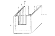
- FIG. 1 is a perspective view showing a substrate cassette used for substrate surface treatment according to an embodiment of the present invention.
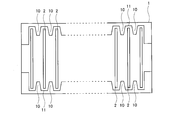
- FIG. 2 is a schematic sectional view showing a substrate cassette used for substrate surface treatment according to an embodiment of the present invention.
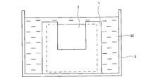
- 3 is a schematic view of a substrate surface treatment apparatus according to an embodiment of the present invention.
- the single crystal silicon substrate 2 sliced from the ingot (as-sliced state) is put into an etching tank 3 containing an alkaline solution 30 such as NaOH as an etching solution and etched.
- an alkaline solution 30 such as NaOH as an etching solution and etched.
- a plurality of as-sliced single crystal silicon substrates 2 are held in a substrate cassette 1, and the whole substrate cassette 1 is put into an etching tank 3 and etched in a batch. Batch processing is performed.
- the material of the substrate cassette 1 is PPS (polyphenylene sulfide), but PTFE (polytetrafluoroethylene), PFA (tetrafluoroethylene / perfluoroalkyl vinyl ether copolymer), FEP (tetrafluoroethylene.
- PTFE polytetrafluoroethylene
- PFA tetrafluoroethylene / perfluoroalkyl vinyl ether copolymer
- FEP tetrafluoroethylene.
- fluororesins such as hexafluoropropylene copolymer
- synthetic resin materials such as polypropylene and polyethylene
- the upper part of the substrate cassette 1 is open so that the substrate 2 can be inserted.
- a plurality of ribs 10 are provided on the side surface of the substrate cassette 1, and the single crystal silicon substrate 1 is inserted and held in the housing recess 11 between the ribs 10 and 10.
- the rib 10 of the substrate cassette 1 is provided with a concave portion or a convex portion in order to reduce the contact area with the single crystal silicon substrate 2 and prevent both from sticking.
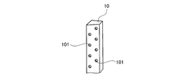
- FIGS. 4A and 4B show a first embodiment of the rib 10 of the substrate cassette 1, FIG. 4A is a perspective view, and FIG. 4B is a cross-sectional view.
- a plurality of holes 101 as recesses are provided on the surface of the rib 10.
- the contact area between the rib 10 and the substrate 2 is reduced, and sticking of both is suppressed.
- the etching solution or the cleaning solution flows between the rib 10 and the surface of the single crystal silicon substrate 2, and sticking between the single crystal silicon substrate 2 and the rib 10 is further suppressed.
- the flow of the etching solution and cleaning solution around the rib 10 is improved as a whole, and uniform etching can be realized. Further, the subsequent etching solution can be easily cleaned.
- FIGS. 5A and 5B show a second embodiment of the rib 10 of the substrate cassette 1
- FIG. 5A is a perspective view
- FIG. 5B is a cross-sectional view.
- a plurality of protrusions 102 are provided on the surface of the rib 10.
- the contact area between the rib 10 and the substrate 2 is reduced, and sticking of both is suppressed.
- the etching solution or the cleaning solution flows between the rib 10 and the surface of the single crystal silicon substrate 2 and sticking between the single crystal silicon substrate 2 and the rib 10 is further suppressed.
- FIGS. 6A and 6B show a third embodiment of the rib 10 of the substrate cassette 1, FIG. 6A is a perspective view, and FIG. 6B is a cross-sectional view.
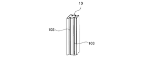
- the rib 10 is provided with standing grooves 103 extending in the vertical direction of the plurality of ribs.
- the contact area between the rib 10 and the substrate 2 is reduced, and sticking of both is suppressed.
- the etching solution or the cleaning solution flows between the rib 10 and the surface of the single crystal silicon substrate 2 and sticking between the single crystal silicon substrate 2 and the rib 10 is further suppressed.
- FIGS. 7A and 7B show a fourth embodiment of the rib 10 of the substrate cassette 1
- FIG. 7A is a perspective view
- FIG. 7B is a cross-sectional view.
- a plurality of lateral grooves 104 are provided on the surface of the rib 10 substantially perpendicular to the height direction.
- the contact area between the rib 10 and the substrate 2 is reduced, and sticking of both is suppressed.
- the etching solution or the cleaning solution flows between the rib 10 and the surface of the single crystal silicon substrate 2 and sticking between the single crystal silicon substrate 2 and the rib 10 is further suppressed.
- FIGS. 8A and 8B show a fifth embodiment of the rib 10 of the substrate cassette 1, FIG. 8A is a perspective view, and FIG. 8B is a cross-sectional view.
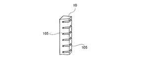
- a plurality of lateral grooves 105 are provided on the surface of the rib 10.
- the lateral groove 105 is formed through both surfaces of the rib 10.
- FIGS. 9A and 9B show a sixth embodiment of the rib 10 of the substrate cassette 1
- FIG. 9A is a perspective view
- FIG. 9B is a cross-sectional view.
- a protruding portion 106 that is continuous in the vertical direction is provided at the tip of the rib 10.
- the contact area between the rib 10 and the substrate 2 is reduced, and sticking of both is suppressed.
- the etching solution or the cleaning solution flows between the rib 10 and the surface of the single crystal silicon substrate 2 and sticking between the single crystal silicon substrate 2 and the rib 10 is further suppressed.
- FIGS. 10A and 10B show a seventh embodiment of the rib 10 of the substrate cassette 1, FIG. 10A is a perspective view, and FIG. 10B is a cross-sectional view.
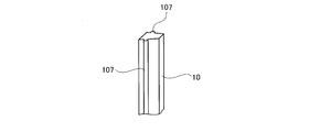
- a protruding portion 107 that is continuous in the vertical direction is provided at the central portion of the rib 10.
- the contact area between the rib 10 and the substrate 2 is reduced, and sticking of both is suppressed.
- the etching solution or the cleaning solution flows between the rib 10 and the surface of the single crystal silicon substrate 2 and sticking between the single crystal silicon substrate 2 and the rib 10 is further suppressed.
- FIGS. 11A and 11B show an eighth embodiment of the rib 10 of the substrate cassette 1, FIG. 11A is a perspective view, and FIG. 11B is a cross-sectional view.
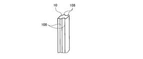
- protrusions 108 that are continuous in the vertical direction are provided at the tip and the center of the rib 10. Providing the protrusions 108 at the tip and center of the rib 10 reduces the contact area between the rib 10 and the substrate 2 and suppresses sticking between the two. Further, the etching solution or the cleaning solution flows between the rib 10 and the surface of the single crystal silicon substrate 2 and sticking between the single crystal silicon substrate 2 and the rib 10 is further suppressed.
- FIGS. 12A and 12B show a ninth embodiment of the rib 10 of the substrate cassette 1, FIG. 12A is a perspective view, and FIG. 12B is a cross-sectional view.
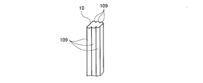
- a stepped portion 109 is provided on the surface of the rib 10 so as to be vertically connected.
- FIGS. 13A and 13B show a tenth embodiment of the rib 10 of the substrate cassette 1
- FIG. 13A is a perspective view
- FIG. 13B is a sectional view
- FIG. 14 shows a substrate cassette according to the tenth embodiment. It is a schematic sectional drawing.
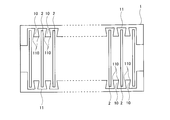
- the rib 10 is formed in an inverted trapezoidal shape in which the side surface of the cassette 1 is narrow and widens toward the center.
- the tip portion of the rib 10 formed in the inverted trapezoidal shape constitutes the convex portion 110.
- the contact area between the rib 10 and the substrate 2 is reduced, and sticking of both is suppressed. Further, the etching solution or the cleaning solution flows between the rib 10 and the surface of the single crystal silicon substrate 2 and sticking between the single crystal silicon substrate 2 and the rib 10 is further suppressed.
- the single crystal silicon substrate 2 is disposed between the receiving recesses 11 of the ribs 10 and 10 of the substrate cassette 1 and the single crystal silicon substrate 2 is held. Then, as shown in FIG. 3, the substrate cassette 1 holding a plurality of single crystal silicon substrates 2 is put into an etching tank 3 containing an etching solution 30 as a processing solution, and the surface of the single crystal silicon substrate 2 is etched. .
- a surface treatment for forming a texture on the single crystal silicon substrate 2 can be performed, and the damage layer can be removed at the same time.
- the single crystal silicon substrate 2 can be etched without sticking to the ribs 10, and a uniform etching process can be performed. Then, the subsequent etching solution can be easily cleaned.
- the surface treatment of the single crystal silicon substrate 2 has been described, but the same treatment can be performed on a polycrystalline silicon substrate.
- a mixed acid solution of boiling acid and nitric acid may be used as an etching solution.
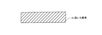
- an n-type single crystal silicon substrate 2 having a resistivity of about 1 ⁇ ⁇ cm and a thickness of about 150 ⁇ m is held in the substrate cassette 1 according to the present invention, and impurities are removed by washing. Then, it is immersed in an etching bath and etched to form a texture structure.
- an RF plasma CVD method is used to form an i-type amorphous silicon layer 22 having a thickness of about 5 nm on the upper surface of the n-type single crystal silicon substrate 2 and a thickness of about 5 nm.
- the p-type amorphous silicon layer 23 is formed in this order.
- an i-type amorphous silicon layer 26 having a thickness of about 5 nm and an n-type amorphous silicon layer 27 having a thickness of about 5 nm are formed in this order on the lower surface of the n-type single crystal silicon substrate 2. .
- a method for forming the amorphous silicon layer a known method such as a vapor deposition method, a sputtering method, a microwave plasma CVD method, an ECR method, a thermal CVD method, or an LPCVD method can be used.
- a vapor deposition method such as a vapor deposition method, a sputtering method, a microwave plasma CVD method, an ECR method, a thermal CVD method, or an LPCVD method
- the amorphous silicon layer amorphous or microcrystalline Si, SiGe, SiGeC, SiC, SiN, SiGeN, SiSn, SiSnN, SiSnO or the like containing at least one of hydrogen and fluorine is used.
- transparent conductive films 24 and 28 made of indium oxide having a thickness of 30 to 100 nm are respectively formed on the p-type amorphous silicon layer 4 and the n-type amorphous silicon layer 8. Respectively. Specifically, it is formed by an ion plating method using a sintered body of In 2 O 3 powder mixed with 3 wt% of WO 3 powder as a target. As formation conditions, a mixed gas of Ar and O 2 is flowed to maintain the pressure at 1.2 to 2.0 Pa, and the formation is performed. The Ar partial pressure is constant at 1.0 Pa. In addition to Ar, an inert gas such as He, Ne, Kr, or Xe or a mixed gas thereof can also be used.
- an inert gas such as He, Ne, Kr, or Xe or a mixed gas thereof can also be used.
- an Ag paste in which silver (Ag) is kneaded into an epoxy resin is formed in a predetermined area on each of the transparent conductive films 24 and 28 to a height of 10 to 30 ⁇ m and a width of 100 to 500 ⁇ m. To do. Thereafter, the silver paste is cured by baking at 200 ° C. for 80 minutes. Thereby, collector electrodes 25 and 29 are formed. In this way, the solar cell according to this embodiment shown in FIG. 18 is formed.
- a p-type polycrystalline silicon substrate is etched to form dense irregularities on the surface.
- the present invention is applied to this substrate surface etching step.
- a liquid containing phosphorus is applied to the surface, the substrate is left in a gas phase atmosphere at 800 ° C. to 900 ° C. for 60 minutes, and phosphorus is infiltrated to form an n + layer.
- an antireflection film 800 ⁇ of TiO 2 is formed on the light receiving surface side.
- an Al paste is printed on the back surface and baked at 750 ° C. to form a p + layer on the surface layer on the back surface (BSF treatment).
- a silver paste is printed on the light-receiving surface, the TiO 2 film on the back surface, and the Al printing fired surface and fired at 700 ° C. to form a silver electrode, whereby a BSF solar cell is manufactured.
Landscapes
- Container, Conveyance, Adherence, Positioning, Of Wafer (AREA)
- Weting (AREA)
- Photovoltaic Devices (AREA)
- Cleaning Or Drying Semiconductors (AREA)
Abstract
リブと半導体基板との間の張り付きを防止し、洗浄液、エッチング液を半導体基板表面にスムーズに流し、均一なエッチングが実現できる方法を提供する。この発明は、基板カセットに設けられた複数のリブ(10)の間に、単結晶シリコン基板を配置し、基板カセットをエッチング液が収容された槽内に浸漬し、単結晶シリコン基板の表面処理を行う半導体装置の製造方法であって、基板カセットのリブ(10)の表面に単結晶シリコン基板との接触面積を低下させる穴部(101)が設けられている。
Description
この発明は、基板の表面処理を行う半導体装置の製造方法に関し、より詳しくは半導体製造プロセスにおける半導体基板の表面処理を行う方法及びそれに用いられる基板カセットに関するものである。
近年、エネルギーの枯渇問題や地球環境問題などから再生可能エネルギーの開発が望まれている。特に、太陽電池を用いた太陽光発電が新しいエネルギー源として注目されている。
ところで、太陽電池などの半導体素子において、その表面はスライスダメージ層の除去等を行い基板表面の品質確保する点、或いは表面形状の形成の点で重要な要素である。基板表面の処理の方法としては、気相や液相における化学反応が利用されることが多い。特に、太陽電池の分野では、エッチング等の表面処理が、スライスされた半導体基板表面のダメージ層の除去や受光面のテクスチャー形成において用いられる。
従来、このエッチング処理は、複数の半導体基板をカセットに入れ、カセットとともに複数の半導体基板がエッチング槽内のエッチング液に浸漬される。太陽電池のエッチング処理に用いられるカセットとしては、特許文献1に記載されているように、複数の半導体基板を収容するために、複数のリブ(または溝)が設けられたものが知られている。
前記リブ(または溝)は、エッチング並びにエッチングの前後の洗浄処理において、半導体基板同士の距離をある程度保持し、良好な洗浄面を得ることにある。
しかしながら、従来の方法では、半導体基板の厚さが薄くなるにつれ、エッチング処理時に、リブ(または溝)に半導体基板が張り付くことがある。また、リブ(または溝)があることにより洗浄液やエッチング液が半導体基板表面に十分に流れず、リブ(または溝)部分にエッチングのムラが発生することがある。
この発明は、リブと半導体基板との間の張り付きや、洗浄液、エッチング液を半導体基板表面にスムーズに流し、均一なエッチングが実現できる方法及びそれに用いる基板カセットを提供することにある。
この発明は、基板カセットに設けられた複数のリブの間に、半導体基板を配置し、前記基板カセットを処理液が収容された槽内に浸漬し、前記半導体基板の表面処理を行う半導体装置の製造方法であって、前記基板カセットのリブ表面に前記半導体基板との接触面積を低下させる凹部または凸部が設けられていることを特徴とする。
また、この発明は、複数の半導体基板を保持して表面処理を行う槽内に浸漬される基板カセットであって、前記基板カセットに設けられた複数のリブと、前記リブ表面に設けられ前記半導体基板との接触面積を低下させる凹部または凸部と、を備えたことを特徴とする。
前記リブ表面に上下方向に延びる凸部を形成すればよく、また、前記リブ表面に溝部を形成すればよい。
また、前記溝部は前記リブ表面に上下方向に沿って形成すればよい。
この発明によれば、エッチング液や洗浄液等の処理液がリブと半導体基板との間に回り込み、半導体基板とリブとの間の張り付きが抑制され、処理液を半導体基板表面にスムーズに流し、均一な基板表面処理が実現できる。
この発明の実施の形態について図面を参照しながら詳細に説明する。なお、図中同一または相当部分には同一符号を付し、説明の重複を避けるためにその説明は繰返さない。
この発明の基板カセットに保持される基板として、単結晶シリコン、多結晶シリコン等の半導体基板が挙げられる。
この実施の形態においては、住宅用太陽光発電システムとして最も普及しており、より一層の低コスト化が望まれる太陽電池用の単結晶シリコン基板を用いた。前記単結晶シリコン基板は、通常、n型或いはp型の極性を有しているが、どちらの極性を有していてもよい。シリコン基板において、p型を与える不純物としては、ホウ素のようなIII族元素又はその化合物が挙げられ、n型を与える不純物としては、リン、砒素等のV族元素が挙げられる。
この発明に係るエッチングプロセスの概略について、図を参照して説明する。図1は、この発明の実施形態に係る基板表面処理に用いられる基板カセットを示す斜視図、図2は、この発明の実施形態に係る基板表面処理に用いられる基板カセットを示す概略断面図、図3は、この発明の実施形態に係る基板表面処理装置の概略図である。
インゴットからスライスされた状態(アズスライス状態)の単結晶シリコン基板2は、エッチング液であるNaOHなどのアルカリ溶液30の入ったエッチング槽3に投入され、エッチングされる。一般的に、大量生産にて自動搬送装置を用いる場合は、アズスライス状態の単結晶シリコン基板2を基板カセット1に複数枚保持させ、基板カセット1ごとエッチング槽3に投入して一括してエッチングするバッチ処理が行われる。
この実施形態では、基板カセット1の材質は、PPS(ポリフェニレンサルファイド)としたが、PTFE(ポリテトラフルオロエチレン)、PFA(テトラフルオロエチレン・パーフルオロアルキルビニルエーテル共重合体)、FEP(テトラフルオロエチレン・ヘキサフルオロプロピレン共重合体)等の各種フッ素樹脂やポリプロピレン、ポリエチレン等の合成樹脂材料を用いても良い。エッチング終了後、基板カセット1ごとエッチング槽3からエッチングされた単結晶シリコン基板2が取り出される。その後、水洗、乾燥が行われる。
図1及び図2に示すように基板カセット1の上部は開口し、基板2を挿入できる構造となっている。図示するように、基板カセット1の側面には、複数のリブ10が設けられ、このリブ10、10間の収容凹所11に単結晶シリコン基板1が挿入され、保持される。
この基板カセット1のリブ10には、単結晶シリコン基板2との接触面積を低下させ、両者が張り付くのを防止するために、凹部または凸部が設けられている。
図4A、図4Bは、基板カセット1のリブ10の第1の実施例を示し、図4Aは斜視図、図4Bは断面図である。図4A及び図4Bに示すように、この第1の実施例では、リブ10の表面には、複数個の凹部としての穴101が設けられている。リブ10の表面に複数個の穴101を設けることで、リブ10と基板2との接触面積が低下し、両者の張り付きが抑制される。さらに、エッチング液や洗浄液がリブ10と単結晶シリコン基板2の表面との間に回り込み、単結晶シリコン基板2とリブ10との間の張り付きがより一層抑制される。この結果、リブ10周辺のエッチング液や洗浄液の流れが全体的に改善し、均一なエッチングが実現できる。さらに、後のエッチング液の洗浄も容易に行なうことができる。
図5A、図5Bは、基板カセット1のリブ10の第2の実施例を示し、図5Aは斜視図、図5Bは断面図である。図5A及び図5Bに示すように、この第2の実施例では、リブ10の表面には、複数個の突起102が設けられている。リブ10の表面に複数個の凸部としての突起102を設けることで、リブ10と基板2との接触面積が低下し、両者の張り付きが抑制される。さらに、エッチング液や洗浄液がリブ10と単結晶シリコン基板2表面との間に回り込み、単結晶シリコン基板2とリブ10との間の張り付きがより一層抑制される。
図6A、図6Bは、基板カセット1のリブ10の第3の実施例を示し、図6Aは斜視図、図6Bは断面図である。図6A及び図6Bに示すように、この第3の実施例では、リブ10の表面には、複数個のリブの上下方向に延びる立て溝103が設けられている。リブ10の表面に複数個の立て溝103を設けることで、リブ10と基板2との接触面積が低下し、両者の張り付きが抑制される。さらに、エッチング液や洗浄液がリブ10と単結晶シリコン基板2表面との間に回り込み、単結晶シリコン基板2とリブ10との間の張り付きがより一層抑制される。
図7A、図7Bは、基板カセット1のリブ10の第4の実施例を示し、図7Aは斜視図、図7Bは断面図である。図7A及び図7Bに示すように、この第4の実施例では、リブ10の表面には、複数個の高さ方向と略垂直に横溝104が設けられている。リブ10の表面に複数個の横溝104を設けることで、リブ10と基板2との接触面積が低下し、両者の張り付きが抑制される。さらに、エッチング液や洗浄液がリブ10と単結晶シリコン基板2表面との間に回り込み、単結晶シリコン基板2とリブ10との間の張り付きがより一層抑制される。
図8A、図8Bは、基板カセット1のリブ10の第5の実施例を示し、図8Aは斜視図、図8Bは断面図である。図8A及び図8Bに示すように、この第5の実施例では、リブ10の表面には、複数個の横溝105が設けられている。この横溝105は、リブ10の両面を貫通して形成されている。表面に複数個の横溝105を設けることで、リブ10と基板2との接触面積が低下し、両者の張り付きが抑制される。さらに、エッチング液や洗浄液がリブ10と単結晶シリコン基板2表面との間に回り込み、単結晶シリコン基板2とリブ10との間の張り付きがより一層抑制される。
図9A、図9Bは、基板カセット1のリブ10の第6の実施例を示し、図9Aは斜視図、図9Bは断面図である。図9A及び図9Bに示すように、この第6の実施例では、リブ10の先端部に、上下に連なる突出部106が設けられている。リブ10の先端部に突出部106を設けることで、リブ10と基板2との接触面積が低下し、両者の張り付きが抑制される。さらに、エッチング液や洗浄液がリブ10と単結晶シリコン基板2表面との間に回り込み、単結晶シリコン基板2とリブ10との間の張り付きがより一層抑制される。
図10A、図10Bは、基板カセット1のリブ10の第7の実施例を示し、図10Aは斜視図、図10Bは断面図である。図10A及び図10Bに示すように、この第7の実施例では、リブ10の中央部分に、上下に連なる突出部107が設けられている。リブ10の中央部分に突出部107を設けることで、リブ10と基板2との接触面積が低下し、両者の張り付きが抑制される。さらに、エッチング液や洗浄液がリブ10と単結晶シリコン基板2表面との間に回り込み、単結晶シリコン基板2とリブ10との間の張り付きがより一層抑制される。
図11A、図11Bは、基板カセット1のリブ10の第8の実施例を示し、図11Aは斜視図、図11Bは断面図である。図11A及び図11Bに示すように、この第8の実施例では、リブ10の先端部と中央部分に、上下に連なる突出部108がそれぞれ設けられている。リブ10の先端部と中央部に突出部108設けることで、リブ10と基板2との接触面積が低下し、両者の張り付きが抑制される。さらに、エッチング液や洗浄液がリブ10と単結晶シリコン基板2表面との間に回り込み、単結晶シリコン基板2とリブ10との間の張り付きがより一層抑制される。
図12A、図12Bは、基板カセット1のリブ10の第9の実施例を示し、図12Aは斜視図、図12Bは断面図である。図12A及び図12Bに示すように、この第9の実施例では、リブ10の表面に、上下に連なる段部109が設けられている。リブ10の表面に段部109を設けることで、リブ10と基板2との接触面積が低下し、両者の張り付きが抑制される。さらに、エッチング液や洗浄液がリブ10と単結晶シリコン基板2表面との間に回り込み、単結晶シリコン基板2とリブ10との間の張り付きがより一層抑制される。
図13A、図13Bは、基板カセット1のリブ10の第10の実施例を示し、図13Aは斜視図、図13Bは断面図、図14は、この第10の実施例に係る基板カセットを示す概略断面図である。図13A、図13B、図14に示すように、この第10の実施例では、リブ10がカセット1の側面側が狭く中央に向かって広くなる逆台形状に形成されている。この逆台形状に形成されたリブ10の先端部が凸部110を構成することになる。逆台形状のリブ10に形成して先端部が凸部110を構成することで、リブ10と基板2との接触面積が低下し、両者の張り付きが抑制される。さらに、エッチング液や洗浄液がリブ10と単結晶シリコン基板2表面との間に回り込み、単結晶シリコン基板2とリブ10との間の張り付きがより一層抑制される。
上記した基板カセット1のリブ10、10の収容凹所11間に単結晶シリコン基板2を配置して、単結晶シリコン基板2を保持させる。そして、図3に示すように、単結晶シリコン基板2を複数枚保持した基板カセット1を処理液としてエッチング液30が収容されたエッチング槽3に投入し、単結晶シリコン基板2の表面をエッチングする。この処理で単結晶シリコン基板2にテクスチャーを形成する表面処理が行なえ、かつダメージ層の除去も同時に行える。さらに、単結晶シリコン基板2は、リブ10に張り付くことなくエッチングが行え、均一なエッチング処理が行える。そして、後のエッチング液の洗浄も容易に行なうことができる。
上記した実施形態においては、単結晶シリコン基板2の表面処理について説明したが、多結晶シリコン基板に対しても同様の処理を行うことができる。尚、多結晶シリコン基板において、テクスチャー形成を行う際には、エッチング液として、沸酸と硝酸の混酸溶液を用いればよい。
次に、この発明の基板の表面処理を用いて太陽電池を作成するプロセスにつき説明する。
まず、図15に示すように、約1Ω・cmの抵抗率と約150μmの厚みとを有するn型単結晶シリコン基板2をこの発明にかかる基板カセット1に保持し、洗浄することにより不純物を除去し、エッチング槽に浸漬してエッチングを行い、テクスチャー構造を形成する。
続いて、図16に示すように、RFプラズマCVD法を用いて、n型単結晶シリコン基板2の上面上に約5nmの厚みを有するi型非晶質シリコン層22と、約5nmの厚みを有するp型非晶質シリコン層23とをこの順番で形成する。
そして、n型単結晶シリコン基板2の下面上に約5nmの厚みを有するi型非晶質シリコン層26と、約5nmの厚みを有するn型非晶質シリコン層27とをこの順番で形成する。
尚、非晶質シリコン層の形成方法としては、蒸着法、スパッタ法、マイクロ波プラズマCVD法、ECR法、熱CVD法、LPCVD法等の公知手法を用いることができる。又、非晶質シリコン層としては、水素、フッ素の少なくとも一方を含む、非晶質又は微結晶のSi、SiGe、SiGeC、SiC、SiN、SiGeN、SiSn、SiSnN、SiSnO等が用いられる。
次に、図17に示すように、p型非晶質シリコン層4及びn型非晶質シリコン層8の各々の上に、30~100nmの厚みを有する酸化インジウムからなる透明導電膜24及び28をそれぞれ形成する。具体的には、WO3粉末を3wt%混入したIn2O3粉末の焼結体をターゲットとして用い、イオンプレーティング法により、形成する。形成条件としては、ArとO2の混合ガスを流して圧力を1.2~2.0Paに保ち、形成する。尚、Ar分圧は、1.0Paと一定とする。Arの他に、He、Ne、Kr、Xe等の不活性ガス又はこれらの混合気体を用いることもできる。
そして、透明導電膜24及び28の各々の上の所定領域にスクリーン印刷法を用いて、エポキシ樹脂に銀(Ag)を練り込んだAgペーストを、高さ10~30μm、幅100~500μmに形成する。その後、200℃で80分焼成して銀ペーストを硬化させる。これにより、集電極25及び29を形成する。このようにして、図18に示すこの実施形態に係る太陽電池が形成される。
次に、多結晶シリコン基板を用いた太陽電池作製プロセスについて、以下に簡単に説明する。
まず、p型多結晶シリコン基板をエッチング処理し、表面に緻密な凹凸を形成する。この基板表面エッチング工程に本発明が適用される。
続いて、リンを含む液体を表面に塗布し、800℃~900℃の気相雰囲気中に60分間前記基板を放置し、リンを浸透させて、n+層を形成する。
続いて、受光面側にTiO2の反射防止膜800Åを形成する。
続いて、裏面にAlペーストを印刷し、750℃で焼成することにより裏面の表面層にp+層を形成する(BSF処理)。
続いて、受光面、裏面の前記TiO2膜および前記Al印刷焼成面上に銀ペーストを印刷して700℃で焼成し銀電極を形成してBSF型太陽電池が製造される。
今回開示された実施の形態はすべての点で例示であって制限的なものではないと考えられるべきである。この発明の範囲は、上記した実施の形態の説明ではなくて特許請求の範囲によって示され、特許請求の範囲と均等の意味および範囲内でのすべての変更が含まれることが意図される。
1 基板カセット
2 単結晶シリコン基板
10 リブ
2 単結晶シリコン基板
10 リブ
Claims (8)
- 基板カセットに設けられた複数のリブの間に、半導体基板を配置し、前記基板カセットを処理液が収容された槽内に浸漬し、前記半導体基板の表面処理を行う半導体装置の製造方法であって、前記基板カセットのリブ表面には、前記半導体基板との接触面積を低下させる凹部または凸部が設けられていることを特徴とする半導体装置の製造方法。
- 前記基板カセットのリブ表面に上下方向に延びる凸部が形成されていることを特徴とする請求項1に記載の半導体装置の製造方法。
- 前記基板カセットのリブ表面に溝部が形成されていることを特徴とする請求項1に記載の半導体装置の製造方法。
- 前記溝部は前記リブ表面に上下方向に沿って形成されていることを特徴とする請求項3に記載の半導体装置の製造方法。
- 複数の半導体基板を保持して表面処理を行う槽内に浸漬される基板カセットであって、
前記基板カセットに設けられた複数のリブと、
前記リブ表面に設けられ前記半導体基板との接触面積を低下させる凹部または凸部と、を備えたことを特徴とする基板カセット。 - 前記リブ表面に上下方向に延びる凸部が形成されていることを特徴とする請求項5に記載の基板カセット。
- 前記リブ表面に溝部が形成されていることを特徴とする請求項5に記載の基板カセット。
- 前記溝部は前記リブ表面に上下方向に沿って形成されていることを特徴とする請求項7に記載の基板カセット。
Applications Claiming Priority (2)
| Application Number | Priority Date | Filing Date | Title |
|---|---|---|---|
| JP2010147039A JP2012015135A (ja) | 2010-06-29 | 2010-06-29 | 半導体装置の製造方法およびそれに用いられる基板カセット |
| JP2010-147039 | 2010-06-29 |
Publications (1)
| Publication Number | Publication Date |
|---|---|
| WO2012002212A1 true WO2012002212A1 (ja) | 2012-01-05 |
Family
ID=45401932
Family Applications (1)
| Application Number | Title | Priority Date | Filing Date |
|---|---|---|---|
| PCT/JP2011/064242 Ceased WO2012002212A1 (ja) | 2010-06-29 | 2011-06-22 | 半導体装置の製造方法及びそれに用いられる基板カセット |
Country Status (2)
| Country | Link |
|---|---|
| JP (1) | JP2012015135A (ja) |
| WO (1) | WO2012002212A1 (ja) |
Cited By (2)
| Publication number | Priority date | Publication date | Assignee | Title |
|---|---|---|---|---|
| CN102629642A (zh) * | 2012-04-13 | 2012-08-08 | 上海超日(洛阳)太阳能有限公司 | 一种防太阳能电池减反射绒面产生黑纹的绒面制备方法 |
| TWI564074B (zh) * | 2014-12-16 | 2017-01-01 | 財團法人工業技術研究院 | 糠醛化合物的氧化反應催化劑組成及其應用方法 |
Families Citing this family (5)
| Publication number | Priority date | Publication date | Assignee | Title |
|---|---|---|---|---|
| JP2015084348A (ja) * | 2012-02-13 | 2015-04-30 | 長州産業株式会社 | 光起電力素子及びその製造方法 |
| JP2013222911A (ja) * | 2012-04-19 | 2013-10-28 | Shin Etsu Chem Co Ltd | 基板処理装置及び基板処理方法、並びに太陽電池の製造方法 |
| JP6016174B2 (ja) | 2012-07-31 | 2016-10-26 | パナソニックIpマネジメント株式会社 | 太陽電池の製造方法 |
| JP2015035502A (ja) * | 2013-08-09 | 2015-02-19 | 三洋電機株式会社 | シリコン基板のエッチング方法 |
| JP6814628B2 (ja) * | 2016-12-22 | 2021-01-20 | Toyo Tire株式会社 | トレッド用トレイ |
Citations (4)
| Publication number | Priority date | Publication date | Assignee | Title |
|---|---|---|---|---|
| JPH02161745A (ja) * | 1988-12-14 | 1990-06-21 | Nec Corp | 半導体ウェーハ用キャリア |
| JPH05291386A (ja) * | 1992-04-10 | 1993-11-05 | Hitachi Ltd | ウェハケース |
| JPH08203992A (ja) * | 1995-01-26 | 1996-08-09 | Sony Corp | 半導体ウェハキャリヤ |
| US6318389B1 (en) * | 1999-10-29 | 2001-11-20 | Memc Electronic Materials, Inc. | Apparatus for cleaning semiconductor wafers |
-
2010
- 2010-06-29 JP JP2010147039A patent/JP2012015135A/ja active Pending
-
2011
- 2011-06-22 WO PCT/JP2011/064242 patent/WO2012002212A1/ja not_active Ceased
Patent Citations (4)
| Publication number | Priority date | Publication date | Assignee | Title |
|---|---|---|---|---|
| JPH02161745A (ja) * | 1988-12-14 | 1990-06-21 | Nec Corp | 半導体ウェーハ用キャリア |
| JPH05291386A (ja) * | 1992-04-10 | 1993-11-05 | Hitachi Ltd | ウェハケース |
| JPH08203992A (ja) * | 1995-01-26 | 1996-08-09 | Sony Corp | 半導体ウェハキャリヤ |
| US6318389B1 (en) * | 1999-10-29 | 2001-11-20 | Memc Electronic Materials, Inc. | Apparatus for cleaning semiconductor wafers |
Cited By (2)
| Publication number | Priority date | Publication date | Assignee | Title |
|---|---|---|---|---|
| CN102629642A (zh) * | 2012-04-13 | 2012-08-08 | 上海超日(洛阳)太阳能有限公司 | 一种防太阳能电池减反射绒面产生黑纹的绒面制备方法 |
| TWI564074B (zh) * | 2014-12-16 | 2017-01-01 | 財團法人工業技術研究院 | 糠醛化合物的氧化反應催化劑組成及其應用方法 |
Also Published As
| Publication number | Publication date |
|---|---|
| JP2012015135A (ja) | 2012-01-19 |
Similar Documents
| Publication | Publication Date | Title |
|---|---|---|
| US9773928B2 (en) | Solar cell with electroplated metal grid | |
| KR101168589B1 (ko) | 계면 활성제를 이용한 실리콘 태양전지의 텍스처링 방법 | |
| CN103681953B (zh) | 制造太阳能电池的方法 | |
| TWI455342B (zh) | Solar cell with selective emitter structure and manufacturing method thereof | |
| CN104025317B (zh) | 以全大气压印刷工艺形成渐变折射率透镜以形成光伏面板 | |
| JP2012015135A (ja) | 半導体装置の製造方法およびそれに用いられる基板カセット | |
| EP2782146B1 (en) | Method for manufacturing a solar cell with reduced potential induced degradation | |
| KR20130084218A (ko) | 나노구조체 및 이를 구현하는 광전지 | |
| US20130125974A1 (en) | Solar cell with metal grid fabricated by electroplating | |
| CN102263152A (zh) | 具有通过电镀制造的金属栅的太阳能电池 | |
| JP5927027B2 (ja) | 光電変換装置 | |
| JP2010123859A (ja) | 太陽電池素子および太陽電池素子の製造方法 | |
| KR20160062004A (ko) | 전해-연마 및 다공화 | |
| JP5945066B2 (ja) | 光起電力素子の製造方法 | |
| CN108028290A (zh) | 光电转换元件、包括该光电转换元件的太阳能电池模块及太阳光发电系统 | |
| CN118335815A (zh) | 太阳能电池及其制备方法 | |
| US8841161B2 (en) | Method for forming flexible solar cells | |
| JP5874675B2 (ja) | テクスチャ形成方法及び太陽電池の製造方法 | |
| JP6254348B2 (ja) | 光電変換装置 | |
| CN103035773B (zh) | 光电转换装置 | |
| JP6502147B2 (ja) | 太陽電池の製造方法および太陽電池モジュールの製造方法 | |
| KR101070071B1 (ko) | 후면 전극형 태양전지 제조방법 | |
| JP2014075418A (ja) | 太陽電池用シリコン基板及びその製造方法、並びに太陽電池 | |
| WO2017010029A1 (ja) | 光電変換装置 | |
| JP2015122347A (ja) | 太陽電池およびその製造方法、太陽電池モジュール |
Legal Events
| Date | Code | Title | Description |
|---|---|---|---|
| 121 | Ep: the epo has been informed by wipo that ep was designated in this application |
Ref document number: 11800677 Country of ref document: EP Kind code of ref document: A1 |
|
| NENP | Non-entry into the national phase |
Ref country code: DE |
|
| 122 | Ep: pct application non-entry in european phase |
Ref document number: 11800677 Country of ref document: EP Kind code of ref document: A1 |